Process Development and Basic Studies of … · and Basic Studies of Electrochemically Deposited...
65
August 2000 NREL/SR-520-28762 V.I. Kaydanov and T.R. Ohno Colorado School of Mines Golden, Colorado Process Development and Basic Studies of Electrochemically Deposited CdTe-Based Solar Cells Annual Technical Report, Phase I 15 May 199814 May 1999 National Renewable Energy Laboratory 1617 Cole Boulevard Golden, Colorado 80401-3393 NREL is a U.S. Department of Energy Laboratory Operated by Midwest Research Institute • Battelle • Bechtel Contract No. DE-AC36-99-GO10337
Transcript of Process Development and Basic Studies of … · and Basic Studies of Electrochemically Deposited...

August 2000 NREL/SR-520-28762
V.I. Kaydanov and T.R. OhnoColorado School of MinesGolden, Colorado
Process Developmentand Basic Studies ofElectrochemically DepositedCdTe-Based Solar Cells
Annual Technical Report, Phase I15 May 199814 May 1999
National Renewable Energy Laboratory1617 Cole BoulevardGolden, Colorado 80401-3393NREL is a U.S. Department of Energy LaboratoryOperated by Midwest Research Institute •••• Battelle •••• Bechtel
Contract No. DE-AC36-99-GO10337

August 2000 NREL/SR-520-28762
Process Developmentand Basic Studies ofElectrochemically DepositedCdTe-Based Solar Cells
Annual Technical Report, Phase I15 May 199814 May 1999
V.I. Kaydanov and T.R. OhnoColorado School of MinesGolden, Colorado
NREL Technical Monitor: B. von RoedernPrepared under Subcontract No. XAK-8-17619-28
National Renewable Energy Laboratory1617 Cole BoulevardGolden, Colorado 80401-3393NREL is a U.S. Department of Energy LaboratoryOperated by Midwest Research Institute •••• Battelle •••• Bechtel
Contract No. DE-AC36-99-GO10337

NOTICE
This report was prepared as an account of work sponsored by an agency of the United Statesgovernment. Neither the United States government nor any agency thereof, nor any of their employees,makes any warranty, express or implied, or assumes any legal liability or responsibility for the accuracy,completeness, or usefulness of any information, apparatus, product, or process disclosed, or representsthat its use would not infringe privately owned rights. Reference herein to any specific commercialproduct, process, or service by trade name, trademark, manufacturer, or otherwise does not necessarilyconstitute or imply its endorsement, recommendation, or favoring by the United States government or anyagency thereof. The views and opinions of authors expressed herein do not necessarily state or reflectthose of the United States government or any agency thereof.
Available electronically at http://www.doe.gov/bridge
Available for a processing fee to U.S. Department of Energyand its contractors, in paper, from:
U.S. Department of EnergyOffice of Scientific and Technical InformationP.O. Box 62Oak Ridge, TN 37831-0062phone: 865.576.8401fax: 865.576.5728email: [email protected]
Available for sale to the public, in paper, from:U.S. Department of CommerceNational Technical Information Service5285 Port Royal RoadSpringfield, VA 22161phone: 800.553.6847fax: 703.605.6900email: [email protected] ordering: http://www.ntis.gov/ordering.htm
Printed on paper containing at least 50% wastepaper, including 20% postconsumer waste

3
Preface
This project, “Process Development and Basic Studies of Electrochemically DepositedCdTe-Based Solar Cells”, which is performed at the Colorado School of Mines (CSM), is part ofthe NREL Thin-Film Partnership Program. The project addresses long-term research anddevelopment issues related to polycrystalline thin-film solar cells. Our general research approachis based on combining activities aimed at improvement of cell performance and stability withactivities aimed at increasing our fundamental understanding of the properties of materialsmaking up the cells: CdTe, CdS, multi-layer back contact, and transparent conducting oxide(TCO) front contact. We emphasize the relation between structural and electronic materialproperties and various processing procedures as well as the microscopic mechanisms responsiblefor the cell performance and its degradation.
We believe that better basic understanding of the specific influence of polycrystallinity,especially for the fine-grain materials like those making up CdTe-based cells, is now one of themost important issues we must address. We need to clarify the role of grain boundaries (GB) inthe film electronic properties as well as the electronic properties of the p-n junction. It isimportant to study and understand the influence of the GB boundaries on the spatial distributionof impurities and electrically active defects as well as on their migration and transformation inthe course of the cell long-term normal operating conditions or under stress conditions inaccelerated stability tests. To fulfill these tasks one needs to develop new methods andtechniques (or adjust existing ones) for material characterization as well as more sophisticatedapproaches to the data analysis and modeling. This report presents studies mostly relevant to theproblems formulated above that were carried out at CSM at Phase I of the project according tothe Statement of Work and Tasks of the Subcontract.
Section 1 presents studies of basic electronic properties of SnO2:F thin films produced usingAPCVD method at CSM in cooperation with Green Development, L.L.C. Transparency andsheet resistance of the films were close to those for the commercially available materials, such as“Nippon Glass” and “Asahi”. Bulk resistivity, Hall and Seebeck (thermopower) effects weremeasured as well as optical properties such as transmittance, reflection, and absorption spectra.Spectrophotometer and multi-angle spectral ellipsometry was used for studies of opticalproperties. Modeling the reflection spectrum and ellipsometry data based on the Drude theoryprovided the plasma frequency and collision frequency data. Comparative studies of Hall effect,Seebeck effect and plasma frequency in the carrier concentration range of 2x10²⁰ to 6x1020 cm-3
were used to determine the electron effective mass and its dependence on the electron energy. Noindication of non-parabolicity was observed in the energy range of 0.25 to 0.75 eV above theconduction band edge. Therefore in our analysis of experimental data we were able to use thetransport phenomena theory specified for parabolic energy spectrum and high degeneracy of theelectron gas. Contribution of the GB to the total measured resistance of the films was estimatedby means of comparison of the Hall and “optical” mobilities and was found negligible for thebest films. Based on thermopower data and temperature dependence of mobility, as well as onthe electron scattering theory, it was shown that scattering on impurity ions screened with freeelectrons controls mobility in the bulk material. Calculations for the mobility value based on thisscattering mechanism are in good agreement with the experimental data if we account for aspatial dispersion of dielectric constant. It was also shown that compensation of the donors bythe acceptor-type native defects may lead to a significant decrease in electron mobility and hence

4
must be avoided when processing the TCO SnO2 films. The section is concluded with an analysisof advantages and shortcomings of various methods for electronic properties characterization.
Section 2 is devoted to the AC characterization of thin polycrystalline CdTe and CdS filmson the insulating substrates, and is predominantly methodological. The major goal of thesestudies was to get an opportunity to separate and study independently the individualcontributions of the GB and intragrain (IG) material to the total film resistance and also measurethe film capacitance. Using a Hewlett Packard 4285A LCR meter and HP-VEE software, wehave developed various procedures for measurements and modeling based on reasonablephysical and electrical models. Measurements on thin films of CdTe prepared in differentmanners and CBD CdS demonstrated the effectiveness of the method. GB and IG resistanceswere measured in dark and light; high photoconductivity was found to be totally due to asignificant decrease in the GB resistance in light. Discussion of capacitance value led to theconclusion that the doping level (space charge density) in the vicinity of the GB is high:∼1017-1018 cm-3. Studies of resistance and capacitance dependencies on bias applied to the samplerevealed features that should be attributed to the increase in the GB electrical charge. Aprocedure was developed that enables one to derive from these dependencies the density of GBelectronic states. For the CdTe films we measured, it was estimated in the range of 1012 to 1013
cm-2eV-1.
Studies of cell degradation under stress conditions are presented in Section 3. They weremostly aimed at searching for manifestations of electromigration of charged impurities/defects.For these purpose stress tests were conducted under various bias conditions (negative, positive,open circuit, maximum power), at enhanced temperature, in dark and light (∼1 Sun). Cells wereprepared on the CdTe/CdS structures supplied by First Solar, LLC, with application ofCu/ZnTe/Au back contact at CSM. The tests revealed considerable differences in degradationrate under different biases. The degradation degree was significantly different for different cellparameters. The stress tests were also conducted with applying different biases in sequence, e.g.,positive after negative, negative after open circuit, etc. In some cases a considerable recovery ofthe degraded parameters was observed. As a whole, results of stress testing provided evidence ofa significant role of electromigration. The results are considered as preliminary and used fordeveloping a program for further, extended and more informative studies.
A brief description of our collaboration with other institutions within the National CdTeTeam framework is presented in Section 4.
Appendices present data on personnel involved in the studies, laboratory improvements, andpublications.

5
Table of Contents
Preface. ................................................................................................................................ 3
Table of Contents ................................................................................................................ 5List of Figures ............................................................................................................... 7List of Tables ............................................................................................................... 7
1. Studies of APCVD SnO2:F Thin Films1.1 Introduction ........................................................................................................ 81.2 Characterization Methods and Techniques ....................................................... .91.3 SnO2 Film Growth and Properties................................................................... .131.4 Basic Electronic Properties of SnO2:F Thin Films
1.4.1 Approximations of the Theory and Verification of Their Validity ..... 161.4.2 Equations for Transport Coefficients and Their Analysis................... 161.4.3 Experimental Results and Discussion ................................................. 23
1.5 Comparison of Different Methods of Characterization.................................... 331.6 Major Results ................................................................................................. .37
2. AC Electrical Characterization of CdTe and CdS Thin Films2.1 Introduction....................................................................................................... 382.2 Film Resistance and Capacitance at Zero Bias.
A Simple Electrical Circuit Model ................................................................... 392.3. Changes in the Film Electrical Parameters under Applied Bias ....................... 442.4. Capacitance Dependence on Bias Voltage ....................................................... 47
2.4.1 Two Mechanisms of the GB Capacitance ........................................... 472.4.2 Capacitance Caused by the Oscillating GB Electrical Charge............ 49
2.5 Major Results and Conclusions ........................................................................ 51.3. Study of Cell Degradation under Stress Conditions
3.1 Technical Approach and Objectives ................................................................. 533.2 Experimental Results and Discussion............................................................... 543.3 Characterization Methods and Techniques....................................................... 573.4 Major Results and Conclusions ........................................................................ 57
4. Team Activities4.1 Characterization of the High Resistance Tin Oxide Films (HRT).................... 584.2 Cells for Stability Tests at the First Solar Facilities ......................................... 584.3 Characterization of Materials Received from First Solar ................................. 58
5. References ............................................................................................................. 59
6. Acknowledgements................................................................................................ 61

6
7. Appendices7.1 Personnel ......................................................................................................... 617.2 Laboratory Improvements ............................................................................... 627.3 Publications ..................................................................................................... 63

7
List of Figures
Figure 1.1 Tools for measuring Seebeck coefficient on TCO thin films .............................11
Figure 1.2 AFM image of SnO2 thin film on Soda Lime glass substrate....................... 15
Figure 1.3 Plasma frequency from both ellipsometry and reflectionmeasurements against carrier concentration for some tin oxide films ............ 25
Figure 1.4 Carrier concentration vs. magnitude of the Seebeck coefficient .................. 26
Figure 1.5 Carrier concentration vs. scattering parameter ............................................. 26
Figure 2.1 Fragment of the thin film equivalent circuit ........................................................39
Figure 2.2 One block equivalent circuit. .............................................................................40
Figure 2.3 Experimental results for the resistance of a CdTe layer demonstratingthe fit to a simple one-block equivalent circuit....................................................40
Figure 2.4 Experimental results for the capacitance of a CdTe layer demonstratingthe fit to a simple one-block equivalent circuit....................................................41
Figure 2.5 Impedance spectroscopy of a CdS layer ..............................................................42
Figure 2.6 Influence of bias applied to the gold electrodes on the CdTe thin
film resistance.................................................................................................. 44Figure 2.7 Influence of bias on the CdTe thin film capacitance measured in “p-mode” . 45
Figure 2.8 Energy-band diagram for two grains of p-type materialand their boundary region (GB........................................................................ 46
Figure 2.9 Equivalent electrical circuit for the polycrystalline film ................................ 49
Figure 2.10 Dependence of the “GB oscillating charge” capacitanceon bias voltage applied to the sample of PVD CdTe thin film .................... 50
List of Tables
Table 1.1 Optimized temperatures for SnO2:F deposition .............................................. 14
Table 1.2 Comparison of commercial SnO2 films and those depositedat CSM by APCVD......................................................................................... 16
Table 1.3 Comparison of the Hall and optical mobility values....................................... 28
Table 1.4 Calculated mobility as a function of dielectric constant. ................................ 31
Table 1.5 Calculated ratio of mobilities in compensated and non-compensatedSnO2 for the same donor concentration, Nd=5×1020cm-3. .................................32
Table 3.1. Changes in the cell parameters as a function of stress test conditions
and length (time) ..................................................................................................55Table 3.2 Stress tests under varied bias ...............................................................................56

8
1. Studies of APCVD SnO2:F Thin Films
1.1 Introduction
Transparent conductive thin film oxides are important basic electronic materials that havenumerous applications, not only as a front contact in photovoltaic modules. Most applicationsrequire high transparency in the visible spectrum. Solar cells and flat displays also require highelectrical conductivity (low sheet resistance) of the films. Today, TCOs in commercial useinclude tin oxide, which is usually doped with fluorine or antimony (SnO2:F, SnO2:Sb), tindoped indium oxide (In2O3:Sn≡ITO), and zinc oxide, usually doped with aluminum (ZnO:Al)[1]. The properties of these materials are adequate for most current applications, but furtherimprovements in both conductivity and transparency are desirable, particularly for solar cells andflat panel displays.
Improving TCOs is challenging because optical and electrical properties are somewhatinversely correlated - optimal performance requires a compromise between the two. Althoughincreasing carrier concentration through extrinsic doping increases electrical conductivity, σ, itdoes so at the expense of decreased transparency, T, in the visible and near IR spectrum due tofree carrier absorption and reflection (shift in the plasma reflection edge). In the figure of meritof TCOs that is commonly used, transparency is weighted much higher than low sheet resistance[2], hence the limit for the doping level is defined by transparency and is usually in the range of~ 5×10²⁰ to 1×1021cm3. The carrier concentration in commercially available TCO's oftenapproaches this limit. It is not practical to increase carrier concentration further, even if it werechemically possible. Thus the only possible way to increase σ (decrease sheet resistance) is toimprove carrier mobility, µ.
Mobility in single crystals is defined by fundamental electronic parameters, such as theeffective mass of free carriers, the dominating scattering mechanism, types and density ofscatterers, etc. In polycrystalline thin film materials the mobility value is also influenced bystructural imperfections, such as grain boundaries, specific point defects, voids, gaps, etc. Allthe factors that determine mobility in TCO thin films have not been investigated thoroughly orcompletely understood. There are large variations in film properties reported for TCO layersmade by similar processing as well as in the estimations of the theoretical limits of mobility thatcould be achieved by optimizing the film structure and processing procedure. This situationexplains one of the major goals of our research - basic studies of SnO2 thin films aimed atclarification of the factors that determine mobility value in real films and estimation of thetheoretical limit.
A wide variety of deposition techniques have been used to deposit TCOs, such asevaporation, sputtering, spray pyrolysis, and chemical vapor deposition (CVD). In our researchatmospheric pressure chemical vapor deposition (APCVD) was used to produce SnO2 thin films.This choice was dictated by several factors:
1. CVD is considered to be one of the best techniques and is widely used for commercialapplications because it is an inexpensive process in terms of the equipment costs. Thereactants are available in high purity form and the dopants can be introduced easily during
9
the deposition. APCVD is convenient and very productive for high-scale manufacturing onlarge area substrates.
2. An APCVD system for deposition on glass substrates of moderate size (4"x4") becameavailable for us due to collaboration with Green Development, LCC.
3. Several specialists at CSM and Green Development, LCC, involved in these studies hadexperience in APCVD deposition of various materials.
Fluorine was chosen as a dopant providing the optimal carrier concentration in tin oxidebecause it is known from the literature that fluorine yields higher mobility and opticaltransmission than the other possible dopant, antimony.
Comprehensive characterization of the films prepared with APCVD and combined analysisof the structural, compositional, optical and electronic properties provided feedback foroptimization of the processing procedure and the APCVD system design.
According to the problems to be studied and general approach formulated above, thisresearch had the following objectives:
• To establish the set of experimental methods that can provide the information we need on thefilm properties.
• To provide the tools necessary for the planned experimental studies.• To revise and optimize processing conditions and improve the APCVD system design.• To perform experimental studies and theoretical analysis of the fundamental properties of the
electronic system in tin oxide thin films, such as electron energy spectrum in the conductionband and free electron scattering.
• To clarify the factors influencing sheet resistance and bulk mobility in the actual SnO2 filmsand evaluate their importance in the sense of improvement of the film electrical properties.
• To develop recommendations regarding the directions of future studies.
1.2 Characterization Methods and Techniques
Film Thickness and Surface RoughnessAccurate measurements of thickness and surface roughness are very important because of
the dependence of optical and electrical measurements on these parameters. In our routinemeasurements, we use a surface profiler (Tencor® P-10). In order to measure the sample usingthe profiler, a step between the substrate and the tin oxide film surface is produced by etching thetin oxide layer using a solution of 10% concentration hydrochloric acid with zinc powder. Thiscombination produces atomic hydrogen, which attacks the stable tin oxide. The reaction isallowed to occur on the surface of the tin oxide for approximately one minute. A position of thefilm is masked by a suitable tape for step preparation. The reaction does not attack theunderlying glass.
In addition, ellipsometry (see Sec. 1.5) provides a good estimation of thickness and roughness,which usually agrees with profiler measurements.
The Film Structure
To characterize the crystalline properties of the films, X-ray diffraction (XRD) was used(Rigaku model Ru-200 with wavelength of 0.1541 nm, 2θ range from 15o to 60o with 0.05o step
10
sizes, and interval of two seconds). Using this equipment we were able to determine thepreferred crystallographic planes for each sample and make an estimate of the grain size. The
latter was estimated based on the Scherrer formula [3]:)cos(
9.0
θλ
BD = , where λ is the
wavelength of the diffracted beam, θ is the angle of the diffracted peak, and B is the peakbroadening in radians at half its maximum intensity.
Scanning electron microscopy (SEM) and atomic force microscopy (AFM) were used for thefilm morphology studies. AFM provides better space resolution and can capture the grain inthree dimensions so that the roughness can be estimated.
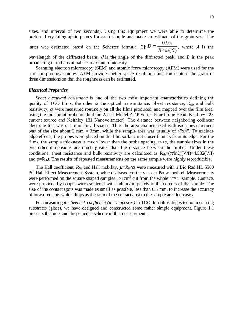
Electrical Properties
Sheet electrical resistance is one of the two most important characteristics defining thequality of TCO films; the other is the optical transmittance. Sheet resistance, Rsh, and bulkresistivity, ρ, were measured routinely on all the films produced, and mapped over the film area,using the four-point probe method (an Alessi Model A 4P Series Four Probe Head, Keithley 225current source and Keithley 181 Nanovoltmeter). The distance between neighboring collinearelectrode tips was s=1 mm for all spaces. Thus the area characterized with each measurementwas of the size about 3 mm × 3mm, while the sample area was usually of 4”x4”. To excludeedge effects, the probes were placed on the film surface not closer than 4s from its edge. For thefilms, the sample thickness is much lower than the probe spacing, t<<s, the sample sizes in thetwo other dimensions are much greater than the distance between the probes. Under theseconditions, sheet resistance and bulk resistivity are calculated as Rsh=(π/ln2)(V/I)=4.532(V/I)and ρ=Rsht. The results of repeated measurements on the same sample were highly reproducible.
The Hall coefficient, RH, and Hall mobility, µ=RH/ρ, were measured with a Bio Rad HL 5500PC Hall Effect Measurement System, which is based on the van der Pauw method. Measurementswere performed on the square shaped samples 1×1cm2 cut from the whole 4"×4" sample. Contactswere provided by copper wires soldered with indium/tin pellets to the corners of the sample. Thesize of the contact spots was made as small as possible, less than 0.5 mm, to increase the accuracyof measurements which drops as the ratio of the contact area to the sample area increases.
For measuring the Seebeck coefficient (thermopower) in TCO thin films deposited on insulatingsubstrates (glass), we have designed and constructed some rather simple equipment. Figure 1.1presents the tools and the principal scheme of the measurements.

11
∆V
∆T
Cool electrode Heated electrode
Chromel
Constantan
-+Sample
Figure 1.1 Tools for measuring Seebeck coefficient on TCO thin films
Two massive copper blocks are placed on the film surface at some distance from each other.One of the blocks is supplied with a heater, which provides heating above room temperature. Thetemperature of the other block is lower and does not differ significantly from room temperaturebecause of the low thermal conductivity of glass and high heat capacitance of the block. Thetemperature difference between the blocks, ∆T, is measured by means of the type-E differentialthermocouple and auto-ranging microvoltmeter DMM (Keithley 197A). ∆T was maintained in therange about 10oC. For the Seebeck voltage (VS) measurement, the copper blocks were connectedwith copper wires to the high input resistance microvoltmeter (Keithly 192 programmable DMM).The Seebeck coefficient of the film material SM was determined as SM= VS/∆T + SR with thereference electrode (copper) Seebeck coefficient SR=SCu=2.09 µV/oK [4,5].
Massive copper blocks, due to their high weight, provided good electrical and thermal contactto the underlying film area. The latter was equipotential and isothermal. That means that wemeasured Seebeck coefficient of the material between the edges of the blocks. Locality of themeasurements was defined by the distance between blocks and usually did not exceed 5 mm. Tocheck how the cylindrical shape of the blocks influences the results of measurement, we performedmeasurements on the same films using rectangular copper blocks placed on the film surface so thatthe edges of the blocks were parallel to each other. No remarkable difference in the results wasobserved. Relocating the copper blocks on the film surface allowed us to map the Seebeckcoefficient over the sample area. It was a method to check the lateral uniformity of the filmproperties in addition to mapping of sheet resistivity.
To verify the accuracy of the Seebeck coefficient measurements using our equipment we usedfoils of standard materials: constantan and nickel. Measurements at different ∆T, from 5 to 20oC,were in a good agreement with each other, and obtained values of SM deviated less than 1% fromthe handbook data [6-8].

12
Spectrophotometry
Transmission, reflection, and absorption spectra were measured by using the Cary 5G UV-Vis-NIR spectrophotometer with a wavelength range from 250 nm to 2500 nm, which can beextended in the IR region by installing additional accessories. Both the total and diffusedcomponent of reflectance can be measured for transmission and reflection by using a differentposition of the sample port and an integrating sphere. The spectrophotometer consists of twoincident light beams (sample and reference), an integrating sphere, and a detector. There are twosources of beams: a quartz halogen lamp for visible/IR region and a deuterium lamp for UV region.These beams have a full dimension 13×5 mm2 and can be reduced to 9×5 mm2. The UV-Visibledetector is R298 photomultiplier tube while NIR detector is an electro-thermally controlled leadsulfide photocell.
The absorption coefficient, α, was calculated based on the transmission (T) and reflection (R)measurements, by using the relation [9, 10]:
t222
t2
eR)T1(
e)RT1(T α−
α−
−+−+=
The diffused component (T and R) is assumed to be very small compared with the specularcomponent. In the wavelength region around the bandgap, where absorption is high (αt >>1), theabsorption coefficient was also calculated by using the relation:
( )T R e t= − −1 2 α
Ellipsometry
A variable Angle Spectroscopic Ellipsometer (a J. A. Woollam Co. Inc. VASE© system)was used for sample characterization. Several angles of incidence (usually 65o, 70o, and 75o) anda large range of wavelengths (usually 280 nm to 1700 nm with 10 nm increments) generated alarge amount of data for more accurate results.
Ellipsometry is based on measuring the change on polarization state of the reflected light
from the surface of the sample. The total electric field vector can be presented by sp sp ˆˆ Ε+Ε=Εr
[11], where Ep and Es are the parallel and perpendicular (to the plane of incident) components ofthe electric field. Two reflectance coefficients are introduced: Rp as the ratio of the reflected Ep
to the incident Ep and Rs as the ratio of the reflected Es to the incident Es. The ratio of these tworeflectance coefficients can be expressed through two ellipsometric angles, ψ and ∆, as
)iexp()tan(R
R
s
p ∆ψ==ρ . These two measurable angles are the most commonly used in
ellipsometry and usually can be determined by using what is called null ellipsometry (source -polarizer - compensator - sample - analyzer - detector).
There are various models [11, 12] that correlate these angles, Fresnel coefficient, complexdielectric constant, or index of refraction (real and imaginary parts), and the layer thickness.Designing a particular model that fits the characterization of the sample, and fitting its opticalconstants to the raw data obtained from ellipsometry, we can then obtain the desired informationon film thickness and the optical properties of each layer in the sample. Unknown parameters inthe model can be varied until the best fitting is obtained which minimizes the root mean squareerror (RMSE) between the created model data and the raw data.

13
There are several layers involved for the TCO samples characterized in this method: theglass substrate, the tin oxide layer, the rough layer on the surface and sometimes the diffusionbarrier between the glass and tin oxide. In order to eliminate back surface scattering whichcomplicates the model, the backside of the substrate was roughened using sandpaper untilopaque. The TCO roughness layer was simulated using 50% of the surface material and 50%voids. Using several angles of incident beam along with a wide range of wavelengths generatesa large amount of data that leads to a higher accuracy fit of the model describing the sample.Increasing the number of layers of a sample will result in complicated models.
Using a Drude model for the SnO2 layer, the plasma frequency, ωp and collision frequency,ωc, can be obtained, which can be used to estimate the carrier concentration and the mobility ofthe sample. Since the SnO2 layer properties can change throughout the material, a linearlygraded Drude model from the bottom to the top of the layer was used in most cases. This canyield different carrier concentrations and mobilities for the top and bottom of this layer. Theparameters allowed to vary in the Drude model were the thickness of the SnO2 and roughnesslayers, along with ωc, ωp, and the complex dielectric constant, ε=ε1+iε2 as a function offrequency. If a diffusion barrier was present, then its thickness could also vary. The opticalconstants of the glass substrate were determined separately and not allowed to vary. The mainmodel used was a linearly graded Drude model, but a second slightly simpler model was alsoused. The second model involved only a single Drude model to which was added a linearlygraded void percentage from the bottom to the top of the samples.
1.3 SnO2 Film Growth and Properties
APCVD System and Chemistry of Deposition Process
We have grown films in a Watkins-Johnson system model 4CVD-75 for atmosphericpressure chemical vapor deposition (APCVD). It has the following features: 4 inch-wide furnace,single injector, bubblers, muffle type furnace and above 700 oC temperature capability. Some partsof the system were modified in the course of our research, mainly the injector design and exhaustsystem. The main control parameters are the reactants gas composition and flow rate, and theinjector and substrate temperature. A four-inch wide continuous belt transports the substratethrough the furnace. The belt speed is adjusted from 0.5 to 15 inches per minute by means of amotor controller in order to produce different thicknesses at given deposition rate. It is connectedto an ultrasonic cleaner and air dryer for continuous belt cleaning.
There are three bubblers connected to the injector through heated pipes for condensationprotection. SnCl4 and H2O are used as precursors, methanol as catalyst, and Freon(Difluoroethane) as a doping source. These materials react at the heated substrate producingSnO2:F thin films:
SnCl4 + n1 H2O + n2 CH3OH + n3 HF→SnO2:F + 4 HCl + n4 H2O + n5 CH3OH + n6 HF
where CH3OH is introduced to moderate the reaction by generating oxygen vacancies, and n1 to n6
are numerical coefficients that balance the reaction.

14
The source materials are in the liquid phase in reservoirs. The vapor pressure of the liquidchemical sources was carefully controlled by immersion of the bubbler vessels inside oil-filledcans. Heating the liquid leads to evaporation and dry nitrogen is then used as a carrier for thechemical vapors. The reservoir temperature, the nitrogen mass flow sensors, and the pipetemperatures control the amount of reactant chemicals. Additional nitrogen lines are addeddownstream from the reservoir outlets so that total gas flow into the injector can be variedwithout affecting the chemical composition or flow. After numerous experiments the optimaltemperatures for the SnO2 deposition were established which are presented in Table 1.1.
Table 1.1. Optimized temperatures for SnO2:F deposition.
Substrate 550 - 600oC
Injector 180 - 240oC
H2O Bubbler 80 - 90oCCH3OH Bubbler 50 - 60oC
CH3OH/H2O Line 100oCSnCl4 Line 75oC
SnCl4 Bubbler 57 - 70oC
The products of the reaction and any unreacted gases are removed with a negative pressureexhaust system. The exhaust system pulls these gases, mainly hydrochloric acid, and transportsthem into a fume scrubber. An excess exhaust flow reduces the deposition rate and producesturbulence of gas flow patterns leading to poor reproducibility of the deposited films. Exhaust flowwas optimized based on computational fluid mechanics modeling performed by C. Wolden [13].
To avoid the non-uniform distribution of temperature across the belt, aluminum oxideceramic plates, which have high thermal conductivity, were used to carry the substrate andprovide better temperature uniformity all over the glass substrate. Large area uniform (5%) tinoxide thin films (t∼400-500 nm) in a large-scale production can now be deposited reproduciblywith the desired properties of the material.
Film Properties
A typical image of a SnO2:F film of a thickness of about 450 nm is presented in Fig. 1.2The average grain size determined with AFM and SEM for many films was in a range from 130to 200 nm. We did not notice any relation between the thickness and the grain size for thicknessbetween 350 to 850 nm. XRD revealed peaks corresponding to (211), (101), (200), and (110)planes with d-space of 1.7735±0.0022, 2.6612±0.0027, 2.376±0.0036, and 3.3723±0.0027 Årespectively, which is in a good agreement with the data on d-space for SnO2 powder for thesame planes: 1.765, 2.644, 2.369, and 3.351 Å [14]. Typically no significant differences in thepeak intensities were observed, hence no conclusions on the preferential orientation could bemade.

15
Figure 1.2 AFM image of SnO2 thin film on Soda Lime glass substrate.

16
Table 1.2 presents the main optical and electrical characteristics of some of the depositedfilms compared with the properties of commercial tin oxide films measured using the samecharacterization equipment
Table 1.2 Comparison of commercial SnO2 films and those deposited at CSM by APCVD.Transparency and haze are averaged over the wavelength range of 500 to 900 nm.
Sample Substrate Thickness
nm
SheetResistance
/Ω ì
Mobility
cm2/Vs
CarrierConcentr.1020 cm-3
Transparency
%Nippon Soda
Lime/SiO2
500 9.5 29.0 4.5 80.5
CSM Soda Lime 370 12.0 25.0 5.6 80.3
CSM Soda Lime 330 14.0 26.0 5.2 82.0Asahi Soda
Lime/SiO2
800 13.5 34.0 1.8 79.0
CSM Soda Lime 690 11.2 29.0 2.9 79.0CSM Soda Lime 610 13.4 29.0 2.6 82.0
In general, our samples have carrier concentration of 1 × 10²⁰ – 6 × 10²⁰ /cm3, and mobilityfrom 14 to 30 cm2/V.s. Spectrophotometer measurements showed that the optical transmission ofour samples in the spectral range of 500-900 nm is around 80% with average reflectance of ∼10%. The optical absorption coefficient, α, of our tin oxide films is very small in this spectralrange. The bandgap value derived from the graphs of photon energy, Eph, versus (αEph)
2 in a highenergy region, varied for different films in the range from 3.95 eV to 4.25 eV. We did notanalyze possible reasons for the variation. The reflectance plasma edge is well pronounced in thelow energy region and shifts toward shorter wavelength as carrier concentration increases inagreement with Drude model (see Sec. 1.4).
1.4 Basic Electronic Properties of SnO2:F Thin Films
This section presents studies of SnO2 thin films aimed at determination and discussion ofthe fundamental parameters of the electron system in this material which are relevant to one ofthe most important characteristics of TCOs, i.e., carrier mobility. Our approach is based onexperimental studies and combined analysis of a variety of transport phenomena including ACconductivity in a high frequency (optical) range. We will start this section with the theoreticalbasis of our studies, then present and discuss the results of experiments.
1.4.1Approximations of the Theory and Verification of Their Validity.
The equations that relate the measured characteristics of a material to the fundamentalparameters, such as carrier concentration, mobility, effective mass, collision time, mean free pathlength, and dominating scattering mechanism, are presented in many publications and textbooks[15, 16]. They were derived based on some simplifications and approximations of the generaltheory. Before using these equations we analyzed the validity of these assumptions and
17
approximations with respect to the specific properties of the heavily doped SnO2 thin filmsknown from literature and our own studies presented in this report.
Quasi-Continuous Electron Spectrum
When the film thickness is very small, one has to discuss a possible influence of thequantum-size effect. The electron spectrum will be quantized if the electron de Brogliewavelength, λe, is comparable to the film thickness. The electron gas in our heavily-dopedmaterial (carrier concentration ranged from 1×10²⁰ to 6×1020 cm-3) is highly degenerate. Henceonly those electronic states contribute to the transport phenomena whose energy is close to theFermi level, that is whose wave vector K is close to the Fermi surface in the K-space.Corresponding λeF values, can be estimated using the formulae: λeF=2π/KF=2π/(3π2n)1/3. For theconcentrations mentioned above, that gives values of in the range of 25 to 43 Å. The typicalthickness of the films studied was in the range of thousands of Angstroms. Thus quantum-sizeeffect can be neglected and the spectrum can be considered as continuous.
Quasi-Classical Approximation
In this approximation the electrons are treated as particles with simultaneously well-definedspace coordinates and momentum/velocity values, and hence the Boltzmann equation formalismcan be used. Good agreement of theory to the published experimental results has been reportedfor many other semiconductor materials with fundamental characteristics similar to those ofSnO2, such as carrier concentration and mobility, effective mass, etc. In particular, Si, some III-Vsemiconductors, PbTe, and PbSe, can be mentioned.
Relaxation Time Approximation
Electric and heat currents are zero in equilibrium when the distribution of electrons over theband states is described by the Fermi-Dirac function:
f0=1+exp[(E-EF)/kBT] -1 (1.1)
where EF is Fermi level and kB is the Boltzmann constant.External fields perturb the distribution from equilibrium while scattering processes drive thedistribution to equilibrium. A stationary non-equilibrium distribution f(K) is formed under theaction of these two factors. To define the non-equilibrium f(K) the Boltzmann equation can beused which in general is an integro-differential one. The mathematical problem is simplifiedsignificantly if the collision integral, Icol, which represents the scattering processes in theequation, can be reduced to a simple analytical form:
[ ])(
f)(f
t
)(fI o
colcol K
KKτ
−−=
∂∂≡ (1.2)
This means that after the external fields have been switched off, the non-equilibrium distributionis relaxing according to the equation:
f (K, t)-fo= [f (K, 0) – fo(K)]exp(-t/τ).
The parameter τ is called the relaxation time and defines the rate of the equilibrium restoration.
The relaxation-time approximation is especially justified when scattering processes areelastic, that is if the change in the electron energy due to the collision is much smaller than the

18
initial energy. That is the case for scattering by impurities, point defects, dislocations, and grainboundaries. For the phonon scattering, relaxation time approximation is always valid if the Fermienergy is much higher than the characteristic phonon energies. That is the case for our materialswhere Fermi energy ranges from 0.25 to 0.75 eV (see Sec.1.4.3) and the maximum phononenergies are lower by an order of magnitude.
Isotropic Electron Spectrum
Analysis of electron transport is rather complicated if the constant energy surfaces in K-space are non-spherical. In this case the effective mass must be in general treated as a tensor thatvaries from one point in the K-space to another. Relaxation time also depends on the Kmagnitude and direction but can be treated as a tensor for some special cases. For the isotropicspectrum, both m* and τ are scalars and their magnitudes depend only on the magnitude of K,that is only on the carrier energy. According to Ref. 17, the constant energy surfaces in SnO2 arerepresented by ellipsoids of revolution with slightly different (about 10%) lengths of the ellipsoidaxes. This very small difference enables us to use the isotropic approximation for SnO2 withoutsignificant errors in calculated transport coefficients. There are two more reasons to make thisassumption: (a) among the transport coefficients we have studied only electricalconductivity/mobility is anisotropic, but the estimate of this anisotropy based on Ref. 18 does notexceed 20-25 %; the Hall and Seebeck coefficients are isotropic for the ellipsoidal constantenergy surfaces; (b) our films do not have some well defined crystallographic orientation, henceeven the conductivity should be averaged over the directions of the grain orientation and bemacroscopically isotropic. Thus we assume that E(K)=E(K).
Parabolic Electron Spectrum
E(K) dependence in general can be approximated by a parabola only in the vicinity of theband extremum, that is close to the band edge. As K value increases, the E dependence on Kbecomes slower than K2. The higher the energy of carriers, the greater the influence of non-parabolicity. For many direct-gap and narrow-gap semiconductors such as InSb, GaSb, PbSe,Hg1-xCdxTe, and Pb1-xSnxTe, non-parabolicity was studied in detail both theoretically andexperimentally (the latter in heavily doped materials or at elevated temperatures) and found wellpronounced and important for transport phenomena (e.g. see [15,16]). One of the most prominentmanifestations of the non-parabolicity is the growth of effective mass with Fermi level. ForSnO2 there were a few attempts to investigate non-parabolicity, but published data arecontroversial, see, e.g., [19] and [20]. We have studied experimentally the effective massdependence on the Fermi level position in a wide range of the latter (from 0.25 to 0.75 eV) bymeans of comparison of the measured Hall and Seebeck coefficients and plasma frequency (seeSec.1.4.3). We did not find any indication of effective mass growth with carrier concentration(Fermi level) increase. Therefore we assume parabolic spectrum for materials we studied.
High Degeneracy of the Carrier Gas and Sommerfeld Approximation
With all the approximations discussed above, the theory comes to the following equationsfor electrical conductivity, the Hall and Seebeck coefficients in the n-type semiconductor:
τ=σ*m
nq 2
;2
2
H qn
1R
>τ<>τ<−= ;
>τ<>τη−<−= )E(
qT
1S (1.3)

19
where η=EF-EC is the Fermi level position with respect to the conduction band edge; <...>symbolizes averaging of a function of E over all the energy band states with a weight function
W=(-∂fo/∂E)·D(E)·v(E)2, where D(E)=[4π·(2m*)3/2/h3]·E1/2 and v=(2E/m*)1/2 are the density ofstates function and electron velocity, respectively, and h is the Planck constant.
The distribution function fo, as well as (-∂fo/∂E), drop to zero exponentially for (E-EF)/kBT>1, hence the finite extent of a band is well simulated by the limit E=∞ when integrating over theband spectrum. The lower band edge will be taken as an origin of energy scale (Emin=0). Thusthe averaging of some function Θ(E) is described by the equation:
∫
∫∞
∞
∂∂
−
∂∂
−Θ=Θ
0
o2/3
0
o2/3
dEE
fE
dEE
fE)E(
)E( (1.4)
The function (-∂fo/∂E) drops exponentially to zero on both sides of E= EF. Indeed,
)/2kT]-[(ETcosh4k
1
E
f2
B
o
η=
∂∂
−
Hence, in the case of high degeneracy, η/kBT>>1, only the states with the energy close to theFermi level contribute considerably to the integrals above. In addition,
101)(f)(fdEE
foo
o =−=+∞−−∞=
∂∂
−∫∞
∞−
Thus the properties of (-∂fo/∂E) function are similar to those of the δ-function if one takes intoaccount that, due to the rapid converging of the integral, replacement of 0 as a lower limit by -∞does not change the integral value. The so-called Sommerfeld approximation is commonly usedfor calculation of the integrals like those in Eq. 1.4, in the case of high degeneracy:
2BE2
22
Eo )Tk(
E6dE
E
f)E( η=η= ∂
Φ∂π+Φ≈
∂∂
−Φ∫ (1.5)
This approximation is valid under conditions: (a) η/kBT>>1 (high degeneracy); (b) magnitude of
Φ(E) does not change considerably within the energy interval ∼kBT where
∂∂−
E
fo is essentially
non-zero; (c) Φ(E) is smooth in this energy interval, that is [Φ-n(∂nΦ/∂En]E=η(kBT)n<<1. If allthese conditions are satisfied, we have to the first non-vanishing approximation:
∫ η=Φ≈
∂∂
−Φ Eo dE
E
f)E( (1.6)
If Φ(E)=(E-η)·Ψ(E), then ΦE=η=0 and we can not neglect the second term in Eq. 1.5. In thiscase one obtains the first non-vanishing approximation:

20
2BE
2o )Tk(
E3dE)E(
E
f)E( η=∂
Ψ∂π=η−
∂∂
−ψ∫ (1.7)
For Φ being a power function of energy: Φ(E)=EP, one obtains from Eq. 1.5:
∫
η−π+η≈
∂∂
− 2B
2PoP )/Tk)(1P(P
61dE
E
fE
When the averaged function Θ(E)=ES (see Eq.1.4), one obtains:
<ES>=ηS[1+(π2/6)S(S+2)(kBT/η)2] (1.8)
In the next section some numerical estimates of possible inaccuracy in calculating transportcoefficients based on the Sommerfeld approximation will be presented.
1.4.2 Equations for Transport Coefficients and Their Analysis
Transport coefficients for the stationary external fields
To calculate σ, RH, and S (see Eqs. 1.3), one needs to know the energy dependence ofrelaxation time, τ. Assuming that τ(E) is a smooth function in the vicinity of Fermi level, we willapproximate it in this region with a power function:
ητηηττ =≡= Er EddrEE ln/ln where)/)(()( (1.9)
The parameter r value depends on the dominating scattering mechanism and usually is referred toas the "scattering parameter".
Now, based on the Sommerfeld approximation and Eqs. 1.8 and 1.9, one obtains
( ) ( )( )
η+π+ητ=⟩τ⟨ 2
B
2
/Tk2rr6
1 (1.10)
( )2B
22
2
2
/Tkr3
1 ηπ+=⟩τ⟨⟩τ⟨
(1.11)
( )⟩⟨
⟩−Ε⟨τ
τη=
( )η
π 22
23
3Tk
r B
+ (1.12)
According to our estimates, the lowest Fermi level value for the materials we studied isη≈0.25 eV which corresponds to n=1×1020 cm-3. At room temperature (T=300 K), kBT=0.0258eV, hence the small parameter, (kBT/η)2, value does not exceed 0.0105. Our analysis of themeasured Seebeck coefficient showed that the scattering parameter value is not greater than1(r≤1). Thus, neglecting the second term in square brackets in Eq. 1.10 leads to an error notgreater than 5%. For the films with n=5×1020cm-3 the estimated inaccuracy is lower by an orderof magnitude. Even smaller inaccuracy comes from neglecting the second term in the right side
of Eq. 1.11. We have compared the ( )
⟩⟨⟩−Ε⟨
ττη
values calculated based on Eq.1.12 (Sommerfeld

21
approximation) with those obtained by using the exact equation for arbitrary degeneracy, whichincludes the Fermi integrals. The difference between the two does not exceed 3% for η/kBT≥10.
Thus, with sufficient precision we can use the Sommerfeld approximation and describetransport coefficients with rather simple equations:
( ) )(*m/nq 2 ητ=σ (1.13)
1H )qn(R −−= (1.14)
)/Tk)(2/3r)(3/)(q/k(S B2
B η+π−= (1.15)
For the parabolic and isotropic model in the Sommerfeld approximation, carrier concentration isdefined by
( )
η
π+ηπ=2
B2
2/33
2/3 Tk
81
h3
*m28n (1.16)
The correction term in the square brackets is less than 1.3% for η/ kBT ≥10, thus we can use thesimplified formulas:
( ) 2/33
2/3
h3
*m28n ηπ= (1.17)
and
3/223/2
n*m2
h
8
3
π=η (1.18)
Substituting the last expression for η in Eq. 1.15, we obtain a useful equation that relates theSeebeck coefficient to the carrier concentration, effective mass, scattering parameter r andtemperature:
( ) 2/3B2B T)n(k
h
*m3/2r/q)27.2(kS −+−= (1.19)
Now let us summarize the results presented above with respect to what information on thefundamental parameters of material can be obtained from the measurements of electricalconductivity, the Hall and Seebeck coefficients. Hall effect measurements provide the carrierconcentration value:
1H )qR(n −−= (1.20)
Combination of conductivity or resistivity, σ or ρ, and the Hall coefficient, RH, gives a mobility,µ, value:
σ=µ HR or ρ=µ /R H (1.21)
Based on Eq. 1.13, mobility can be defined as
*m/)(qqn/ ητ=σ=µ (1.22)

22
Mean free path length of a carrier, l, is the product of a mean free path time (relaxationtime), τ, and the carrier velocity, v: l=τv= q/)(Pq/)(v*m)( ηµ=ηµ=ηl ,
where P(η) is a momentum value for the electron with the energy equal to the Fermi energy. Itcan be easily calculated from the known carrier concentration using the formula:
3/13/1 hn)8/3()(P π=η . Thus the mean free path length can be determined from measurements ofRH and σ by using either of the two equations below:
q/nh)8/3()( 3/13/1 µπ=ηl (1.23)
3/43/2
H3/1 q/Rh)8/3()( σπ=ηl (1.24)
The expression for the Seebeck coefficient (Eq.1.19) contains three fundamental parametersof a material: effective mass, m*, scattering parameter, r, and carrier concentration, n. If two areknown, the third one can be determined from S measurement. In our study we used this equationto derive the scattering parameter which is a signature of the dominating scattering mechanism.Carrier concentration was determined by Hall measurements, and effective mass value wasdetermined from comparison of the Hall and plasma frequency measurements.
AC Electrical Conductivity (Plasma and Collision Frequencies)
In this section we will consider the electrical current induced by a time-dependent (non-stationary) electric field. We will base our analysis on the approximations discussed in Sec. 1.4.1and shown to be valid for the heavily doped SnO2. Briefly, we assume the electron spectrum iscontinuous and isotropic; dissipation of momentum occurs due to scattering of electrons bydefects or phonons; scattering processes can be treated in the relaxation time approximation; andthe electron gas is degenerate. The latter means that only electrons with energy close to theFermi energy contribute to electrical transport, and hence dynamic properties (effective mass,m*) and collision time, τ, or collision frequency, ωc=1/τ, are the same for all those electrons.These approximations enable us to use the Drude model, which is commonly applied to the ACconductivity and optical properties analysis in metals.
AC conductivity is a complex value and depends on the frequency of the electric field
( )ωτ
σωσi−
=1
0 =ωτ
τim
nq
−∗ 112
(1.25)
High electrical conductivity in metals and heavily doped semiconductors, and itsdependence on frequency, significantly influences optical properties of these materials, inparticular the transparency and reflectivity spectra. The wave equation contains a complexdielectric constant with the real and imaginary parts presented by:
ω+ωω
−ε=−=ε′=ε ∞ 2c
2
2p22 1Re kn ;
ω+ωωωω
ε==ε ′′=ε ∞ )(2Im
2c
2
c2pnk
Here n and k are refractive index and extinction coefficient respectively, and ε∞ is the "high-frequency" dielectric constant for which the bound electrons are responsible. The equationsinclude two characteristic parameters that are totally defined by free (conductive) electrons.Those are the collision frequency, ωc=1/τ, and the plasma frequency, ωp, which is a naturalfrequency of oscillations of the electron gas as a whole. The latter is given by equation
23
ωp=[4πq2n/(m*ε∞)]1/2.
When the frequency of an electromagnetic wave comes close to the plasma frequency, thenreflectivity and transparency of the material can change dramatically. If ωc<<ωp, then to a firstapproximation ε ≈ ε’= ε∞ (1-ωp
2/ω2). For real and negative ε (ω<ωp), the solutions to the waveequation decay exponentially in material; i.e. no radiation can propagate. When ε is positive (ω>ωp), solutions become oscillatory, and the conductor should become transparent. Thus at ω=ωp
there should be observed a sharp change in reflectivity which is known as "plasma reflectivityedge" and also in transparency. For real conductors, ωc/ωp is usually not so small, thereforereflectance does not change so sharply when frequency crosses the ωp value. Analysis of themeasured optical spectra allows us to determine plasma and collision frequencies. That providesan independent method for measurement of carrier concentration and mobility if the effectivemass is known. Indeed,
n=ωp2m*ε∞/4πq2 (1.26)
As to mobility, it can be calculated based on the measured value of ωc=1/τ and equation (1.22)so that
µ=(q/m*)/ωc (1.27)
1.4.3 Experimental Results and Discussion
Plasma Frequency and Seebeck Coefficients vs. Hall Concentration. Effective mass.
The objective of studies presented in this section is to determine the effective mass value andits dependence (or independence) on the carrier concentration. The effective mass knowledge isimportant for further analysis of mobility and scattering mechanisms. As to the m*(n) dependence,it is an indicator of whether the formulas presented in Sec. 1.4.2 could be applied to this analysis.The effective mass that appears in the equations for the transport coefficients and Fermi level-concentration relation, is defined by the equation
dP
dE
P
1
*m
1 ≡ (1.28)
where KP h= is the electron momentum. To analyze the influence of non-parabolicity it isconvenient to present the E(P) dependence in the form:
P2/2m0*=E[1+Γ(E)] (1.29)
where m0* is the limiting value of the effective mass when energy drops to zero. Within theenergy range, where the contribution of Γ can be neglected (parabolic spectrum), the effectivemass is constant and equal to mo*, the density of states function is D(E)=4π(2mo*/h2)3/2E1/2, andthe carrier concentration at high degeneracy is defined by n=(8π/3)(2mo*/h2)3/2η3/2. In the rangeof higher energies, where Γ value is not negligible, one has:
[ ]dE/Ed)E(1*m*m o Γ+Γ+= (1.30)
[ ]dE/Ed)E(1E)h/*m2(4)E(D 2/12/32o Γ+Γ+π= (1.31)

24
[ ] 2/32/32/32o )(1)h/*m2)(3/8(n ηΓ+ηπ= (1.32)
Since Γ(E)>0 and dΓ/dE>0, the effective mass value increases with energy, density of statesincreases with energy more rapidly than in the parabolic case, as well as the carrier concentrationdoes with the Fermi level. Conversely, the Fermi level increases with carrier concentrationslower than in the parabolic case.
Let us now consider how non-parabolicity influences the expressions for the transportcoefficients presented and discussed in Sec. 1.4.2. As long as the electron gas is highlydegenerate (η/kBT>>1), the expressions obtained in the Sommerfeld approximation (Eq. 1.5) byneglecting the term ∝ (kBT/η)2, such as those for R, µ, and ωp, preserve their form although noweffective mass is a function of the Fermi level position, that is of concentration:
1H )qn(R −−= , )(*m/)(qqn/ ηητ=σ=µ ,
∞εηπ=ω
)(*m
nq4 2
p .
At the same time an inaccuracy of these expressions due to neglecting the term ∝ (kBT/η)2 canincrease. In contrast, for the Seebeck coefficient it is essential to preserve the second term in theSommerfeld approximation. The new equation for the Seebeck coefficient contains Γ(E), dΓ/dE,and d2Γ/dE2 terms calculated at E=η. Thus, to analyze the Seebeck coefficient we need firstdetermine the Γ(E) function.
We did that by means of measuring and comparing Hall concentration and ωp values on theset of the SnO2 films with different doping levels. As the carrier concentration increases, theFermi level also increases, no matter whether the band is parabolic or not. The Hallconcentration varied in a range of 1.8×10²⁰ to 5.6×1020 cm-3, which provided considerablevariation in the Fermi level position. Because of the high n value and also based on thermopowermeasurements, one could conclude that the electron gas in all the samples is highly degenerate.
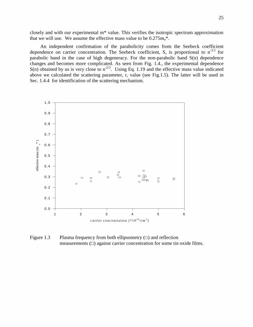
Figure1.3. presents m*(n). Plasma frequency was measured by both spectrophotometry andellipsometry measurements. Effective mass was calculated by using Eq. 1.26 with ε∞=4 derivedfrom our ellipsometry measurements, which is very close to the literature data. It is seen thatwithin the spread of the experimental points the m* value is constant, which means that noconsiderable deviation from parabolicity takes place for our material in the carrier concentrationrange indicated above (and also in corresponding range of the electron energies). This is a veryimportant result, which enables us to use the simple parabolic band theory in further analysis ofthe experimental data.
The effective mass value determined is m*=(0.28±0.03)mo. According to [17], thelongitudinal and transverse effective mass components (that is parallel and perpendicular to therevolution axis of the ellipsoidal constant energy surface) are: m7*=0.234m0 and m⊥*=0.299m0.When averaged over all directions, that provides the value of the "effective mass ofconductivity", mc*, which defines the plasma frequency and mobility for the ellipsoidal constantenergy surface: 1/mc*=1/3[(1/m7*)+(1/m^*)]. The result of calculation is: mc*=0.274m0*. Itshould be noted, that for the ellipsoidal constant energy surface the so called "density of stateseffective mass", md*, is defined as md*= (m7* m^*
2)1/3. This mass is included in the expressionsfor density of states, carrier concentration and Seebeck coefficient. Calculated for the sameeffective mass components, md*=0.276m0. Thus, md* and mc* values coincide with each other
25
closely and with our experimental m* value. This verifies the isotropic spectrum approximationthat we will use. We assume the effective mass value to be 0.275mo*.
An independent confirmation of the parabolicity comes from the Seebeck coefficientdependence on carrier concentration. The Seebeck coefficient, S, is proportional to n-2/3 forparabolic band in the case of high degeneracy. For the non-parabolic band S(n) dependencechanges and becomes more complicated. As seen from Fig. 1.4., the experimental dependenceS(n) obtained by us is very close to n-2/3. Using Eq. 1.19 and the effective mass value indicatedabove we calculated the scattering parameter, r, value (see Fig.1.5). The latter will be used inSec. 1.4.4 for identification of the scattering mechanism.
c a rr ie r c o n c e n tra tio n (* 1 0 2 0/cm 3)
1 2 3 4 5 6
effe
ctiv
e m
ass
(m o*
)
0 .0
0 .1
0 .2
0 .3
0 .4
0 .5
0 .6
0 .7
0 .8
0 .9
1 .0
Figure 1.3 Plasma frequency from both ellipsometry (Ì) and reflectionmeasurements (Æ) against carrier concentration for some tin oxide films.

26
ca rrie r co n ce n tra tio n (cm -3 )* 1 0 2 0
See
beck
coe
ffic
ient
(
µV
/ o K
)
2 0
3 0
4 0
5 0
2 431 .5 5 6
Figure 1.4 Carrier concentration vs. magnitude of the Seebeck coefficient .In the double-log. scale, the dependence is represented by thestraight line with a slope corresponding to S∝n-2/3
c a r r i e r c o n c e n t r a t i o n ( * 1 0 2 0 / c m 3 )
1 2 3 4 5 6
scat
teri
ng p
aram
eter
(r)
0
1
2
3
Figure 1.5 Carrier concentration vs. scattering parameter

27
Resistivity and Mobility (Influence of the Grain Boundaries)
A significant difference is usually observed between mobility (µ=[qρn]-1) values measuredon single crystal and polycrystalline samples of the same material (the same composition, carrierconcentration, etc.). For example, resistivity measured on CdS or CdTe polycrystalline filmscould be several orders of magnitude higher than that for single crystals. This difference isusually attributed to the influence of the grain boundaries (GB). Electronic properties of thematerial in the GB region may be significantly different from those in the bulk of the grains.Deep electronic levels that exist at the interface between two grains trap the majority carriers andhence acquire some electrical charge, which provides a potential barrier for the majority carriers.Thus the GB behaves like two Schottky diodes connected back-to-back.
It is common to treat the problem of the GB influence on resistance in terms of "GB-scattering". This terminology is not always correct and sometimes can be misleading. Indeed,frequency of scattering, 1/τ, is an important parameter that in combination with the effectivemass determines the mobility value. Carriers are scattered by impurities, point defects,dislocations, by phonons (scattering in the grain bulk, or B-scattering) and also by GB (GB-scattering). For several coexisting scattering mechanisms, the total collision frequency is the sumof the partial ones:
GBB321 /1/1.../1/1/1/1 τ+τ=+τ+τ+τ=τ
The individual contribution of the GB scattering can be evaluated by comparison of 1/τGB andtotal scattering frequency, 1/τ. For this purpose it is convenient to rewrite the previous equationin terms of mean free paths, li = τi v. Velocity, v, for high degeneracy is the Fermi velocity that isthe same for all the electrons contributing to the transport phenomena. Thus
GBB /1/1/1 lll += ,
where lB is a free path for the B-scattering and lGB is that for the GB-scattering. The latter is ofthe order of the grain size, dG, while the l value can be calculated based on the carrierconcentration and mobility data by using Eq. 1.23. The highest l value we obtained in this way isabout 50 Å, while the grain size in our films is in the 103 Å scale. Thus 1/l>>1/lGB~1/dG, hencethe GB-scattering can be neglected.
A different approach to discussion of the GB influence on the sample resistivity is based onmodeling the polycrystalline material as a two-phase system. One phase is the material insidegrains (bulk material), and the other (high resistivity) phase is the material in the GB region.When traveling through the sample under the influence of the electric field, an electron iscrossing consequently grains and grain boundaries. Hence the electrical circuit of the sampleconsists of resistors, RB and RGB, representing bulk material and GB, respectively, and connectedin series. When measuring DC resistivity, with either the four probe or van der Pauw method, wemeasure the sum of these two types of resistances. Thus the Hall mobility in general should belower or at least the same as the real bulk mobility:
BGB
BH R/R1+
µ≈µ (1.33)

28
Mobility can be also determined by using the effective mass and collision time (momentumrelaxation time) values, the latter derived from optical measurement. We call this mobility theoptical mobility:
copt *m
q
*m
q
ω=τ≈µ (1.34)
Collision frequency is the actual frequency of scattering and is influenced by grain boundariesonly if lGB and lB values are comparable, which is not the case for our films as shown above,hence µopt≈µB.
Table 1.3 Comparison of the Hall and optical mobility values.
Sample # Thickness(nm)
Hall carrier conc.(1020cm-3)
Mobility (cm2/Vs)µH µopt
1 110 5.9 4.5 212 60 4.0 4.5 323 90 2.4 3.3 294 370 5.6 25 265 500 4.6 29 306 470 3.1 11.5 12
Table 1.3 presents the Hall and optical mobility values for several typical films. It is seenthat for the first three samples (low thickness, small grain size) µH is significantly smaller thanµopt which indicates a significant influence of the grain boundaries, while for the last three (largerthickness) these values are practically the same, within the accuracy of measurements andmodeling. For these films, the contribution of the GB to the measured resistivity can beneglected. The data on the films like these were used for the analysis of the bulk scatteringmechanism.
Bulk Scattering Mechanism
To identify the scattering mechanism we will start with the well known and widely usedsignatures of the scattering mechanisms, such as the temperature dependence of mobility andscattering parameter, which is defined by Eq. 1.9. If effective mass is independent of temperature,then temperature dependence of mobility is defined by two factors. The first one comes from thetemperature dependence of the density of scatterers. It is clear that for scattering by impurities andcrystal structure defects the scatterer density does not depend on temperature. This dependenceexists only for scattering by phonons whose concentration increases with temperature. The secondfactor is defined by two issues: (a) relaxation time dependence on energy and (b) temperaturedependence of the energy of the carriers that contribute mostly to the transport, <E>. For the non-degenerate carrier gas (classical statistics) this energy is proportional to temperature: <E>~ kBT. Forhigh degeneracy <E>≈η and to the first approximation the Fermi level dependence on temperatureshould be neglected.

29
Relaxation time dependencies on energy (hence, scattering parameter) and on temperaturefor various scattering mechanisms were studied theoretically and believed to be defined preciselyfor the parabolic band model, e.g., see [15, 16]. Below are presented scattering parameter valuesand temperature dependencies of mobility (the latter for high degeneracy) predicted by theory forthe most common scattering mechanisms:
Acoustic phonon scattering:r = -1/2, µ∝T-1;
Optical phonon scattering:For temperature below Einstein temperature, ΘE, r=0, µ∝exp(t/ΘE);For temperature well above ΘE, r=1/2, µ∝T-1;
Scattering by the neutral hydrogen-like impurity centers: r = 0, µ∝T0;
Scattering by point defects with the δ(r)-type scattering potential: r= -1/2, µ∝T0;
Scattering by impurity ions with 1/r-type Coulomb scattering potential: r = 3/2, µ∝T0;
We have measured Hall mobility in temperature range of 300 to 5000C. No dependence ontemperature was found. Based on this result we must exclude all the phonon scatteringmechanisms and focus on scattering by defects/impurities. For high carrier concentrations likethose in our samples, the most probable mechanism is scattering by impurity ions because thedensity of impurity ions is the same as the free carriers density, or even higher if there is somecompensation. To check this assumption we must look at the scattering parameter. Its valuedetermined from Seebeck coefficient measurements is presented in Figure 1.5. The valueobtained (r=0.9±0.2) is higher than the predicted ones for all the mechanisms listed above,except ion impurity scattering. At the same time it is lower than that indicated above for thismechanism. The discussion below is aimed at explanation of this discrepancy.
The Coulomb scattering potential of the impurity ion is screened due to:
1. Polarization of the electronic shells of the atoms surrounding the impurity atom; dielectricconstant corresponding to this screening mechanism is the high-frequency dielectric constant,ε∞ ; its value for SnO2 is close to 4.
2. Polarization of the lattice (displacement of the lattice ions toward and outward the impurityion), characterized by εL component.
3. Screening by free carriers (SFC): free carriers are pulled closer to impurity ion (if theircharge sign is opposite to that of impurity ion) or pushed out (if the charge signs are thesame).
In insulators or slightly doped semiconductors the third mechanism of screening can beneglected and the screened Coulomb potential of an impurity atom is described by
ro
QU
ε= (1.35)
where Uis the magnitude of scattering potential, Q is the magnitude of the impurity ioncharge, r is a distance from the center of the impurity ion, and εo=ε∞+εL is a static dielectric

30
constant. In SnO2 εo≈10. In metals or heavily doped semiconductors the SFC mechanism canplay a significant role and the scattering potential is described by:
)or/rexp(ro
QU −
ε= (1.36)
where ro is the screening radius for SFC which is defined for highly degenerate semiconductorsby
( ) 3/1
22
2
o n3/q*m16
hr π
π
ε= ; ( ) 6/12/1o
2/15o n*m/m1065.3r −− ε×= (1.37)
The difference between Equations 1.35 and 1.36 leads to the difference in scatteringparameter value for the Coulomb potential screened and unscreened with free carriers. Tocalculate the scattering parameter, r, value for our materials we will use the theory developed in[21-24]. The dependence of relaxation time on energy for scattering by the impurity ions withSFC can be written in the form:
2/3
Fi4
2
E)E(Nq
*m2)E(
Φπ
ε=τ (1.38)
where
( )ξ+
ξ−ξ+=Φ1
1ln)E( F ; ( )2oFrk2=ξ (1.39)
3/13/12F n)3(k π= (1.40)
Function Φ(ξ) in Eq.1.38 reflects the influence of SFC; kF (Eq.1.40) is the Fermi wave vectormagnitude. Based on Eqs.1.38 and 1.39, as well as on the definition of scattering parameter, (seeEq.1.9), we have derived the expression for the scattering parameter for the scatteringmechanism under consideration:
( ) )(
1
12
3
lnd
lnd
2
3r
2
2
E ξΦξ+ξ−=
ξΦ−= η= (1.41)
The scattering parameter values calculated for n=1×1020cm-3 and n=5×1020cm-3, m*=0.275mo,and ε=εo=10 are presented below:
n=1×1020cm-3: η=0.26 eV; kF=1.5·107 cm-1; ro=10.2 Å ⇒ r=0.9
n=5×1020 cm-3: η=0.76 eV; kF=2.5·107 cm-1; ro=7.5 Å ⇒ r=1.0
The obtained values of the scattering parameter are close to those obtained from theSeebeck coefficient data (see Fig.1.5). At the same time, based on the values of screening radius,ro, one can see an additional problem to be discussed. Indeed, due to the screening by freecarriers, the scattering potential (see Eq.1.36) turned out to be localized in the region of the orderof the unit cell. If so, the problem is what dielectric constant value should be used whencalculating ro and τ. The screening effect caused by displacement of the lattice ions, Sn+4 and O-2,depends on how many coordination spheres are involved in the ionic screening. To provide theeffect corresponding to the "static dielectric constant", εo, the ion displacement must occur in

31
many unit cells surrounding the impurity atom. This is not the case if the perturbing potential islocated in the region close to one unit cell. Thus we must suggest that the effective dielectricconstant that should be put in our calculations is lower than εo. Therefore we have recalculated ro
and scattering parameter with ε=ε∞=4 (the lowest possible ε value) . The results are as follows:
n=1×1020cm-3: ro=6.5 Å ⇒ r=0.7; n=5×1020 cm-3: ro= 4.8 Å ⇒ r=0.8
It is seen that the scattering parameter does not change considerably and stays close to theexperimental value. The real effective dielectric constant should be somewhere between εo andε∞, hence the scattering parameter between the values calculated for the limiting ε values. Thusone can conclude that the dominating bulk mechanism of scattering is the scattering by impurityions screened with free carriers.
Calculation of Mobility in the Bulk of the Grains
Studies presented above provided us with the information that allows calculating the carriermobility and comparing the calculated and measured data. For calculations the equation
)(*m/)(q ηητ=µ (1.42)
was used where the effective mass was assumed to be isotropic, independent on carrierconcentration (hence on η=EF-EC) and equal to 0.275 m0. Relaxation time, which generallydepends on carrier concentration that is on η, was calculated by using Eqs.1.38-1.40. Carrierconcentration was assumed to be =5×1020cm-3 which is close to that for the best SnO2 TCOsamples. The Fermi energy value, η, corresponding to this concentration, calculated by using Eq.1.18, is equal to 0.76 eV. Because of the uncertainty in the effective dielectric constant value(due to the spatial dispersion) mentioned above, we calculated µ value for different ε in the rangefrom ε∞ to εo. The results of calculations are presented in Table 1.4. We assumed nocompensation, that is the density of scatterers, Ni in Eq.1.38, is equal to the carrier concentration.
Table 1.4 Calculated mobility as a function of dielectric constant. n=5×1020 cm-3; compensationdegree β=0
ε ro (Å) µ (cm2/V·s)10 7.2 838 6.7 606 5.8 405 5.3 324 4.8 23
It is seen from the table that (a) the SFC screening radius, ro, is really small, hence we needto use dielectric constant value lower than εo, and (b) mobility calculated with ε=5 is close to theexperimental data (around 30 cm2/Vs). If the measured mobility is so close to theoreticallycalculated, then one may conclude that the achieved level of mobilities is close to the limitingone, and there is no much room for the mobility increase by improvement of processingtechnology. A conclusion of this kind would be of great importance for industry if there were notsome uncertainty about the dielectric constant value that should be used for calculation ofmobility.

32
Another source of uncertainty is the compensation problem. One can not be sure that thecompensation degree for the samples we studied experimentally was zero. If the compensation isconsiderable, then in our calculations of mobility we must use the density of the scatterersgreater than the carrier concentration. Indeed, Ni=Nd+Na, n=Nd-Na, where Nd, Na, and Ni are thedensities of donors, acceptors and impurity ions, respectively. If we designate the compensationdegree as β≡Na/Nd, and mobility in the non-compensated material (β=0) as µ0, then the mobilityin compensated material with the same carrier concentration, µ(β), can be written as
µ(β)=µ0[(1-β)/(1+β)] (1.43)
It is seen from this equation that even for a non-significant compensation degree, the measuredvalue of mobility could be considerably lower than that for the uncompensated material with thesame carrier concentration. Table 1.5 shows the calculated decrease in mobility due to increasein compensation degree for the given donor concentration.
Table 1.5 Calculated ratio of mobilities in compensated and uncompensated SnO2 for the samedonor concentration, Nd=5×1020cm-3.
Comp. degree (β) Carrier Conc. (n, 1020cm-3) µ(β)/µ0
0.0 5 10.2 4 0.70.4 3 0.480.6 2 0.30.8 1 0.15
Unfortunately our deposition system did not permit precise control of the fluorine dopantcontent. We also could not measure directly donor and acceptor concentrations in the preparedfilms. However as an indirect evidence of the compensation influence we will present below thedata on mobility for several samples with different carrier concentrations.
To exclude a possible influence of grain boundaries we selected samples for which the Halland optical mobilities differ only slightly from each other (less than 7%). We compared twogroups of samples prepared at different times and under slightly different conditions. The firstgroup consists of three samples with almost the same parameters: thickness (averaged thickness<t>=450 nm), carrier concentration (<n>=5.3×1020cm-3), and mobility (<µ>=29.6 cm2/Vs). Theother group also consists of three samples with common parameters and is characterized by<t>=510 nm, <n>=3.1×1020 cm-3, and <µ>=12.6 cm2/Vs. Calculation of mobility based on theassumption of zero compensation for both groups leads to a mobility value higher for the firstgroup by only about 10 % because of higher concentration and more pronounced SFC. Let usnow suppose that compensation is absent in the first group (Nd1=n1), and the donor concentrationin the second group is the same as in the first one (Nd2=Nd1=Nd). If so, compensation is the onlyreason why in the second group carrier concentration is lower, and compensation degree can beestimated as β=(Nd-n2)/Nd=(n1-n2)/n1= 0.42. According to calculations like those presented inTable 1.5, the ratio of mobilities should be: µ2/µ1=0.45 which is in a good agreement with theexperimental ratio, 0.425.
33
If all the samples we studied experimentally were compensated, then we must compare thetheoretically calculated mobility with the measured value corrected by a factor (1+β)/(1-β)>1. Inthis case, the coincidence of the calculated and corrected experimental data will take place athigher values of the effective dielectric constant, ε. Thus there are two sources of the uncertaintywhen calculating mobility: (a) spatial dispersion of dielectric constant that should be analyzedtheoretically in the future studies; (b) possible influence of compensation which should bestudied experimentally.
1.5 Comparison of Different Methods of Characterization
For high scale manufacturing of TCOs, routine testing techniques necessarily include sheetresistance and spectral transmission measurements. Often people need much more detailedinformation on the properties of the films in connection with the varying preparation conditions,especially at the stage of research and development. For applications where high transparencyand conductivity are required it is desirable to maximize the ratio of electron mobility to carrierconcentration. Measurements of sheet resistance or even bulk resistivity themselves do not allowus to separate these parameters, and we need additional measurements. Resistivity inpolycrystalline materials can be greatly influenced by the presence of the grain boundaries, gapsbetween grains, voids, etc. It is desirable to estimate the influence of these factors. In this studywe have used various methods and techniques for determination of the same parameters, e.g., theHall and Seebeck effects and plasma frequency for measurement of the free carrierconcentration, or Hall plus resistivity and collision frequency for determination of the carriermobility, etc. In this section we will try to compare various methods for TCO thin filmcharacterization and discuss their advantages and shortcomings based both on theory and on ourown experience of their application.
Carrier Concentration
Hall effect measurement is the most direct method for determination of the free carrierconcentration. It is easy to apply to the TCO thin films. However there are several sources ofinaccuracy and uncertainty when using this method. If the carrier concentration fluctuatesspatially, but the sample is uniform in all other respects, the Hall measurement providesconcentration value averaged over the sample volume. But, if mobility is laterally non-uniform(which often occurs in thin films), the average carrier concentration is underestimated.Inaccuracy can increase due to not well-defined geometry of a sample, non-uniformity of itsthickness, presence of voids, microcracks, and gaps between grains. It should be also mentioned,that the Hall method is destructive (we need to cut from the whole produced plate a small sampleof a regular shape and solder to it electrical contacts).
Seebeck effect measurement is an indirect method for the carrier concentrationdetermination. It could be used routinely if S(n) dependence is empirically established by meansof comparative measurements of the Hall and Seebeck on the series of high quality samples withdifferent carrier concentrations. If we have a reliable S(n) calibration, then we can replace theHall measurements by the Seebeck measurements. Some important features and advantages ofthe Seebeck coefficient measurements should be mentioned and discussed here:

34
1. The Seebeck coefficient measurements do not demand some special geometry of the sampleand can be performed on the samples of an arbitrary shape and size and even on the samplesof non-uniform thickness.
2. The measured Seebeck coefficient is not influenced significantly by the voids, microcracks,grain boundaries. For samples containing such kinds of defects, information obtained aboutthe carrier concentration by using S(n) calibration curve can be more reliable than thatobtained from the direct Hall effect measurements.
3. Only those portions of the sample material, where the temperature gradient exists, contributeto the measured Seebeck voltage, VS. For our arrangement where the entire sample is held atroom temperature, except the region close to the heated copper block, only the materiallocated in the vicinity of the block contributes to the measured signal. Thus, if the block issharpened (thermoprobe), we are able to measure the local Seebeck coefficient. The spatialresolution is on the order of the size of the contact between the thermoprobe and a sample. Itcould be easily made less than 1 mm. By relocation of the thermoprobe on the film surfacewe can map the Seebeck coefficient (and hence the carrier concentration) distribution overthe sample area.
4. This method is not destructive: the measurements can be performed on the produced plate;putting the reference electrodes (copper blocks in our equipment) on the sample surface andrelocating them does not damage the film.
5. Each measurement of the local Seebeck coefficient takes a short time if the temperature ofmeasurements is close to room temperature and the tools for measurement are like thosedescribed in Sec. 1.2.
Plasma frequency measurements also can be used to get information on carrierconcentration. This method is also indirect, similarly to the Seebeck measurements. Theequation, which relates plasma frequency to the carrier concentration, is simpler than that for theSeebeck coefficient. The only parameter we need to know to calculate the concentration from theωp data is the effective mass. If this parameter is not well defined, an empirical approach can beused as in the case of the Seebeck effect. Comparative measurements of plasma frequency andthe Hall concentration should be conducted on a series of high quality samples with varyingcarrier concentration to obtain n(ωp) calibration.
Plasma frequency can be determined from the location on the wavelength scale of a sharpincrease in reflectance. Our studies demonstrated that the reflectance increase for heavily dopedSnO2 samples is sharp enough for the satisfactorily accurate ωp determination. More accuratedata can be obtained when modeling the reflectance and transmittance spectra based on theDrude model. Including the Lorentz oscillators into the model should in principle improve thetheory and experiment fitting, but in our studies no considerable manifestations of the Lorentzoscillators were observed.
To determine ωp we used not only a reflectance spectrophotometry but also multi-anglespectral ellipsometry. The latter derives its sensitivity, which is greater than a simple reflectionmeasurement, from determination of the relative phase change in a beam of reflected polarizedlight. Ellipsometry is more accurate than reflectance intensity measurement because the absoluteintensity of the reflected light does not have to be measured. There was a good agreementbetween parameters obtained with ellipsometry measurements and those obtained from the

35
reflectance spectra. The modeling we used for ellipsometry provided an opportunity also toreveal non-uniformity in ωp over the film thickness. This was used to screen samples when weselected the uniform samples for the comparative Hall, Seebeck and plasma frequency studies. Ingeneral, this method can be used if non-uniformity is the issue to be detected and studied.
As compared to the Seebeck effect, the optical methods have some shortcomings. While theformer can be applied to samples of unlimited sizes, the equipment used for opticalcharacterization puts some limitation on the sample size. Samples with area not higher than2"×4" could be tested in our spectrophotometer and for the ellipsometry the limitation was12"×12". Spatial resolution, for the Seebeck measurements, is determined by the sharpness of thethermoprobe tip. The diameter of the contact spot can be easily made less than 1 mm. As tooptical testing, the spatial resolution is limited by the light beam cross section. Themeasurements and the raw data treatment are much easier for the Seebeck measurements. Theequipment/tools for these measurements are much simpler, less expensive and more durable.
A more fundamental limitation on the optical methods application comes from the spectralrange of the instruments we use. Our instruments cover visible light range, near UV and near IRranges, e.g., the spectral range of our spectrophotometer is of 250 to 2500 nm. For the SnO2
samples with carrier concentration in the range of 1×10²⁰ to 6×1020cm-3, the plasma frequencycould be measured with an acceptable accuracy. As the concentration decreases, the plasmafrequency shifts farther to the IR range (ωp∝n1/2) and the accuracy drops. For the concentrationsbelow 1×1019 cm-3, measurements of ωp become unreasonable unless we use aspectrophotometer for the far IR.
Carrier Mobility
Usually mobility is defined as µ = (q·n·ρ)-1, where n is the carrier concentration and ρ is themeasured electrical bulk resistivity. Concentration can be determined by the Hall, Seebeck andplasma frequency measurements as discussed above. Electrical resistivity measured by commonDC or low-frequency AC methods is often overestimated. If the sample structure is not perfect,especially if the sample is not a single crystal, imperfections can contribute much to themeasured ρ value. The presence of voids, microcracks, non-uniformity of the film thickness oreven the surface roughness increase the resistance of the sample and lead to underestimation ofthe carrier mobility of the substance. In a polycrystalline material, grain boundary regions can bemuch more resistive than the material inside the grains. Studies of CdTe and CdS thinpolycrystalline films have shown that the mobility determined through DC measurements ofresistivity can be by orders of magnitude lower than the real mobility of the carriers inside thegrains. High-frequency (up to tens of MHz) AC measurements we use in our laboratory providean opportunity to separate the individual contributions to the resistance of grain boundaries andintragrain material. The electrical equivalent circuit for the grain boundary region contains aresistor and capacitor connected in parallel. The former at high frequencies is shunted by thelatter and becomes much lower than the intragrain resistance. Unfortunately, this method couldnot be applied to the TCOs where the resistance of the grain boundaries turned out to be verysmall and shunting by capacitance is not effective.
Another approach for the real intragrain material mobility measurement was used in thisresearch which was based on optical characterization of the material. Carrier mobility can becalculated if the effective mass value and collision time (momentum relaxation time) are known:µ = q τ / m*. We have determined the m* value from ωp(n) dependence which is in a good

36
agreement with the literature data. Collision time was determined by the spectroscopicellipsometry measurements as a reciprocal of the collision frequency: τ =ωc
-1. To distinguishthe mobility value obtained in this way we designate it as µopt contrary to the Hall mobility, µH.
Collision frequency is defined by all the collision (scattering) processes which lead to thedissipation of the electron momentum, hence µopt is a real mobility inside the grain material.Grain boundaries do not influence this parameter if the grain size is much greater than the meanfree path length, hence µopt can be higher (or even much higher) than µH.
Which of the two methods for the mobility determination should be used, depends of theobjectives of the material characterization. The optical mobility and optical resistivity, ρopt =(q·n·µopt)
-1, are the real mobility and resistivity of the intragrain material. The DC resistivity is acharacteristic of the film itself with all the structural defects like grain boundaries, voids, etc.,and defines the TCO quality with respect to technical applications.
Limitations on “optical” mobility measurements are the same as for the plasma frequency.Collision frequency is derived from the spectral optical characteristics in the spectral range closeto the plasma frequency.
Film Thickness and Surface Roughness
Film thickness and roughness were measured by means of the Surface Profiler and also byusing the ellipsometry. The results obtained by these methods are in a satisfactory agreementwith each other for the films with a thickness in a range which is typical for the technicalapplications, that is above 350 nm. For films with thickness of around 100 nm, agreement wasmuch worse. It is difficult right now to conclude which method is more accurate, butreproducibility was better for the ellipsometry measurements. Another advantage ofellipsometry is that this is a non-destructive method while measurements with the profilerdemanded removal of some portion of the film to provide a step whose height was measured bythe profiler.
Conclusions
Various methods of material characterization can be used for getting an information onoptical, electrical and structural properties of TCO thin films.
In addition to common Hall effect measurements, carrier concentration can be derived fromSeebeck coefficient, S, measurements by using S(n) calibration. This is a reliable, non-destructive method that can be applied to the thin film samples of an arbitrary shape and sizeand to materials in a wide carrier concentration range. Relocation of a sharpenedthermoprobe over the film surface allows to measure and map local carrier concentration. Incombination with the four-point probe measurements of sheet resistance it also provides anopportunity to map local mobility.
Optical characterization can provide an information not only on optical properties of thematerial (spectral transmittance, reflectance and absorbance) but also on the electronicparameters, such as carrier concentration and mobility. The latter two can be derived fromplasma frequency and collision frequency with modeling based on the Drude model.
Comparison of the Hall and optical mobility values is the basis for estimates of grainboundary contribution to the measured DC resistivity of a sample.

37
Multiangle spectral ellipsometry provides wide options for material characterization. Fromthese measurements the data can be derived on carrier concentration, mobility in theintragrain material, film roughness and thickness, as well as optical transmittance,reflectance, absorbance, and dielectric constant. This method is the most preferable forcharacterization and studies of multilayer materials, like TCO/buffer layer/insulatingsubstrate (glass or polymer).
1.6 Major Results
1. SnO2: F thin films on soda lime glass substrates were prepared using APCVD techniquewith transparency and sheet resistance close to those for the best commercially availablematerials.
2. A variety of methods were used to characterize electronic properties of the films, including:
- Sheet resistance (four-point probe measurements)
- Hall effect, Hall mobility and bulk resistivity (van der Pauw geometry)
- Seebeck coefficient (thermopower)
- Plasma frequency and collision frequency (spectrophotometry and multiangle spectralellipsometry.
3. The results of combined electrical and optical measurements were analyzed based on theelectron transport theory specialized for the highly degenerate electron gas. In this waybasic parameters of the electronic system were determined:
- Effective mass in a wide energy range; no indications of non-parabolicity were found
- Contribution of grain boundaries to the total film resistance in plane, which was foundalmost negligible for the films with high mobility
- Mobility inside the grains and dominating scattering mechanism (by impurity ionsstrongly screened with free carriers
4. For this scattering mechanism, bulk mobility was calculated which turned out to be close tothe experimentally determined one if one assumes the effective dielectric constant is closeto 5, that is significantly lower than the static dielectric constant for this material (ε0≈10).This result seems reasonable if to take into account that the free carrier screening radius andlocalization of the perturbing impurity ion potential are close to the unit cell size. Thatmakes screening with displacement of the host ions less effective (spatial dispersion ofdielectric constant).
5. Possible effect on mobility of the donor dopant compensation by native defects wasestimated. It was shown that eliminating compensation is an important issue for preparationof TCO films with high mobility (low sheet resistance).
6. Various methods for TCO thin films characterization were compared, their advantages andshortcomings were analyzed.

38
2. AC Electrical Characterization of CdTe and CdS Thin Films
2.1 Introduction
Measurements of the complex impedance (Z) on polycrystalline films are aimed at separationand independent studies of grain boundaries (GB) and intragrain (IG) material. The basic idea of themethod is that a polycrystalline film consists of two phases with very distinct electrical properties.One phase is the IG material and the other is presented by the GB regions with the potential barriersfor the majority carriers. GB is characterized by high resistance and also by capacitance provided bya depletion semi-insulating regions adjacent to the GB. The grain is assumed to be electricallyequivalent to a resistor, whereas the GB is electrically modeled as a resistor in parallel with acapacitor. At low frequencies the film impedance is almost totally defined by the GB resistance. Athigh frequencies the GB capacitor effectively shunts the GB resistor, so that the measured resistancetends to the IG resistance. Thus measurements in a wide frequency range provide an opportunity toseparate individual contributions of GB and IG material to the sample resistance and determine theGB capacitance. The method proved to be effective for studies of CdTe thin films on insulatingsubstrates [25, 26]. GB resistance and capacitance are to be studied under different conditions, suchas temperature, illumination intensity and spectrum, and bias. These studies presumably shouldprovide information on the electronic properties of the GB, like potential barrier height, doping levelin the vicinity of GB, density of GB states, etc. Knowledge of these properties that can vary underdifferent processing procedures, is important for understanding the influence of grain boundaries onsolar cell performance and developing new approaches to improvement of the cell quality.
In order to be able to measure complex impedance/admittance, an LCR meter (Hewlett Paccard4285A) and an HP-VEE (Visual Engineering Environment) software have been purchased.
The instrument provides measurements in the frequency range from 75 kHz to 30 MHz; thesoftware runs the LCR meter using HP-IB communicating standard. Using this software, about 20experimental procedures have been developed, which enabled us to run a variety of experiments formeasurement of different electrical parameters of a sample. The main measurement types performedroutinely are:
1. Impedance magnitude,Z, and phase angle, Θ, as functions of frequency.
2. Real, Re(Z), and imaginary, Im(Z), parts of impedance as functions of frequency.
3. Resistance and capacitance as functions of frequency.
4. Z and Θ as functions of bias voltage.
5. Re(Z) and Im(Z) as functions of bias voltage.
6. Resistance and capacitance as functions of bias voltage.
7. Im(Z) as a function of Re(Z) ("Impedance Spectroscopy").
8. Resistance and capacitance as functions of time after switching on and off light or bias (transient processes).

39
All the parameters listed above characterize a sample as a whole. These parameters should beanalyzed based on the physical and mathematical models that represent to some approximation realelectronic properties of a polycrystalline thin film. This is a major goal of the studies presented inthis report. We started with the simplest model (equivalent electrical circuit) and found that fittingof the model with experimental results is satisfactory which enabled us to estimate the GBresistance and capacitance as well as resistance of the IG material. Then we went further, usingmore complicated electrical circuits and sophisticated physical models that led to more precisefitting of the data and provided more detailed information on the GB electronic properties andelectronic processes that occur at the GB region. Based on the same approach, we will continue ourstudies developing new experimental procedures and new models as we obtain new results on filmsdifferently prepared and treated.
2.2 Film Resistance and Capacitance at Zero Bias. A Simple ElectricalCircuit Model
Preliminary measurements aimed at comparison of different measurement procedures andapproaches to the results treatment were performed on CdTe and CdS thin films. CdTe films wereprepared with physical vapor deposition on glass substrates (IEC at the University of Delaware) andtreated in different ways at CSM. CdS films were deposited on glass substrates by CBD and treatedat our facilities. The evaporated golden strips were used as electrodes providing semi-ohmic, lowresistance electrical contacts to CdTe and high resistance rectifying contacts to CdS. In completedarkness the samples usually exhibit a very high resistance that makes impossible accuratemeasurements in the whole frequency range. To avoid this, we used to perform measurements underillumination that provides a controllable lowering of the GB resistance. The results of measurementswere being compared with those calculated for an equivalent circuit consisting of "blocks", eachblock is a GB resistor R1 in parallel with a GB capacitor C1, both in series with another, IG resistorR2. One block represents one grain with one grain boundary. In reality, any sample is made ofthousands of these blocks.
C1
R2
R1
Figure 2.1 Fragment of the thin film equivalent circuit

40
Measuring the electrical resistance and capacitance of CdTe and CdS samples with assumingan equivalent circuit of only one block (Fig. 2.2), yielded a reasonably good fit to the calculated data(Figs. 2.3 and 2.4). Measurements were done in two LCR meter modes: "p" which suggests that thecircuit is composed of a resistor and capacitor in parallel, and "s" which suggests the circuitcomposed of a resistor and capacitor in series.
R2
C1 R1
Figure 2.2 One block equivalent circuit. R1 and C1 represent resistance and capacitance of the wholegrain boundary network. R2 represents resistance of the intragrain material
Figure 2.3 Experimental results for the resistance of a CdTe layer demonstrating thefit to a simple one-block equivalent circuit
CdTe - serial/parallel resistance
1.E+02
1.E+03
1.E+04
1.E+05
1.E+06
1.E+07
1.E+08
0.0001 0.001 0.01 0.1 1 10 100 1000
Frequency (MHz)
Res
ista
nce
(O
hm
)
Rp(meas)
Rs(meas)
Rp(calc)
Rs(calc)

41
Figure 2.4 Experimental results for the capacitance of a CdTe layer demonstrating the fit to asimple one-block equivalent circuit
Relations between the displayed Rp, Cp, Rs and Cs values, and the sample parameters, R1, C and R2
derived from the impedance and admittance analysis for the circuit in Fig. 2.2 are as follows:
Rp=R2+[R1/(1+α)]·1+α/[1+(R2/R1)(1+α)]; Cp=C·(1+α)/[1+R2/R1(1+α)]2+α;
Rs=R2+R1/(1+α); Cs=C·(1+α)/α;
where α=(R1Cω)2 and ω is an angular frequency.Good fitting means that using "lumped"parameters is an acceptable procedure for these measurements, and that in our case, a single blockmay represent quite adequately a polycrystalline material composed of a lot of grains. The fittedresults make it possible to extract R1, C1 and R2 from the measurements.
Incorporating more than one block yielded even better fits, which gives a simple means forevaluating the range of distribution of the values of these parameters. Very good fitting was foundwhen three blocks were incorporated with the same C1 and R2 values while R1 values for the threeblocks related to each other as 1:1.5:2. Since resistance of the GB depends exponentially on thebarrier height, it may be concluded that standard deviation of the latter from the average is verysmall.
The same parameters can be yielded by other frequency dependence measurements, e.g., Re(Z)and Im(Z) or Z and Θ. What kind of measurements is preferable depends on the relations
CdTe - serial/parallel Capacitance
1.E-13
1.E-12
1.E-11
1.E-10
1.E-09
0.0001 0.001 0.01 0.1 1 10 100 1000
Frequency (MHz)
Cap
acit
ance
(F
arad
)
Cp(meas)
Cs(meas)
Cp(calc)
Cs(calc)

42
between values of R1, R2 and C. A very helpful and attractive method is measurement of Im(Z) as afunction of Re(Z). This measurement yields a graph that has a semi-circle shape (see Fig. 2.5).
Figure 2.5 Impedance spectroscopy of a CdS layer. Solid line shows a semi-circle representingcalculation for one block circuit. Dotted line shows calculation for two-block circuit,which demonstrates a spread in R1 of about a factor of 2.5. The tail at low frequenciesis attributed to the electrodes.
This feature makes it very convenient for analysis. For the simple, one-block equivalentelectrical circuit, the maximum value of Im(Z) is equal to R1/2; intersection of the graph with theRe(Z) axis at high frequency yields the R2 value; the angular frequency, ω0, at which maximumIm(Z) is observed, provides the C1 value: C1=(R1·ω0)
-1.
Incorporating more than one block yielded even better fits, which gives a simple means forevaluating the range of distribution of the values of these parameters. Another advantage of thismethod is the ability to eliminate the contribution of high resistance electrode contacts to the derivedthin film parameters. To include these contacts, our equivalent electrical circuit must be composedof two blocks connected in series. The first one (R1, C1, R2, as before) represents the film betweenthe electrodes; the second (Rcont+Ccont in parallel) represents contacts. The total measured impedanceis the sum of those for the two blocks. Each block itself provides a semicircle dependence of Im(Z)on Re(Z), but the frequencies corresponding to their maxima, ω0
film and ω0cont , may be quite
different. The large area contact capacitance, Ccont, is orders of magnitude higher than that of thefilm. If the contact resistance is comparable or higher than that of the film, then ω0
film >>ω0cont,
contribution of the contacts to the impedance is negligible in the frequency range around and aboveω0
film , and the parameters R1, R2 and C derived from the measurements are not influenced by thecontacts (see Fig. 2.5). This feature may make a four-point measurement unnecessary.
CdS
0
5000
10000
0 10000 20000 30000
Re(Z) (Ohm)
-Im
(Z)
(Oh
m)
X(calc)
X(meas)
Circle
13-Jan-99
Sample: PG6-1Light: Lamp 20cm
R1=11.5+4.5 kOhmC1= 4 pF
R2= 2.5 kOhm
Low Freq.High Freq.
R1
R1+R
2

43
The results presented above (RGB, RIG, CGB values and their dependence on illumination)enable us to make some qualitative conclusions and numerical estimates of the electronic propertiesof the films.
1. The contribution of the IG material to the total measured resistance is 103-106 times lower thanthat of the GB, so that this resistance is almost totally defined by the GB. The GB potential barrierheight, φB, values estimated based on the thermionic emission theory are of the order of severaltenths of an electron-volt, in agreement with the estimates in [26].
2. Capacitance, C, of a sample is mostly defined by the capacitance of the GB regions.Capacitance measured on the CdTe sample treated with CdCl2 was about 10-12F. The film thickness,t, was about 3.5 µm, distance between gold electrodes, l, was 0.2 mm, the size of the sample in thethird direction, b, was about 1cm, the average grain size, d, was about 3µm. If we simplify byassuming that the film consists of the square shaped grains of the same size, d, then a specificcapacitance (per unit area) of a single GB, Csp can be estimated as
d
l
btCCsp
1= (2.1)
For the film parameters listed above, one obtains Csp≈ 4×10⁻⁷F/cm2. Knowledge of the specificcapacitance and the barrier height enables us to estimate the doping level, ND, in the GB vicinity.Indeed, Csp=εε0/2WGB, where WGB is a depletion width on each side of a GB which depends on ΦB
and ND: WGB=(2εε0ΦB/qND)1/2. Thus we have:
ND,cm-3=5.66×1032×ε-1×(ΦB/e),V×(Csp,F/cm2) (2.2)
Taking ε≈10 for CdTe and assuming ΦB/e≈0.5V, we obtain ND≈1×1018cm-3. This number is threeorders higher than the CdTe doping level value that is obtained by C-V measurements onCdTe/CdS solar cells. Let us suppose that due to simplified topography of GB network weoverestimate Csp value by the factor of 2. Even then we have ND≈2.5×1017cm-3, which stillsignificantly exceeds the C-V data. L. Woods [26] has also concluded that doping level in thevicinity of GB in CdTe is on the order of 1017cm-3. He derived his estimates from analysis oftemperature dependence of the GB conductance based on a thermally-assisted tunneling model.
3. The IG material resistivity estimated from our measurements is of the order of 10 Ω-cm.Resistivity calculated as ρ=(qnµ)-1 has a value of ≈100Ω-cm for n=1015cm-3 and mobility as highas 60 cm2/Vs which is the highest hole mobility value measured in CdTe single crystal. Highdoping level in the GB vicinity may be a possible reason for this discrepancy. Indeed, the highconductivity layers along the grain boundaries parallel to the current direction can effectivelyincrease the conductance of the grains, so that the effective IG resistivity decreases.
4. All CdTe and CdS films demonstrated high photoconductivity. This effect is morepronounced for films that have a higher dark resistance. By varying the illumination intensity(usually we it was not higher than 0.125 Sun) we were able to decrease R1 by orders of magnitude,while R2 was almost not effected and remained orders of magnitude lower than R1. The measuredfilm capacitance demonstrated only a small increase under illumination that did not exceeded 10-15%. These results leadsto the following conclusions:
The high photoconductive effect in polycrystalline CdTe and CdS thin films is totally due to adecrease in the GB resistance. The latter depends exponentially on ΦB, therefore even a small

44
change in ΦB caused by light can lead to a dramatic change in RGB. For example, for ∆ΦB≈0.1eV, one has at room temperature ∆RGB/ RGB≈50. The GB depletion layer width is proportionalto φB
1/2, so that 10% increase in C corresponds to 20% decrease of φB.
Illumination with the intensity we used (<1Sun) does not lead to a remarkable increase in carrierconcentration inside the grains. This conclusion is consistent with doping level (ô1014-1015 cm-
3) in our films and the lifetime for the photogenerated carriers (∼10-9 sec) derived from PLintensity decay.
2.3 Changes in the Film Electrical Parameters under Applied BiasRepeating measurements with the application of a DC bias, showed that the film parameters,
R1 and C1, are dependent on the applied voltage. The procedures 4-6 in the list presented abovemade it possible to measure the sample electrical parameters at various biases. The resultsdemonstrated a strong dependence on bias particularly in the lower frequency range. Thisdependence becomes less and less pronounced and then vanishes as frequency increases (see,e.g., Figures 2.6 and 2.7). X(Z)-R(Z) plots also demonstrate a considerable increase in filmresistance and capacitance. Changes in the GB resistance and capacitance may be attributed tothe increase of electrical charge accumulated in the GB states under influence of bias. This effectwas discussed and analyzed in numerous publications, see, e.g., [27, 28, 31].
Figure 2.6 Influence of bias applied to the gold electrodes on the CdTe thin film resistance.Illumination intensity is 0.125 Sun. Resistance was measured in “p-mode”.
CdTe - Rp
0.E+00
1.E+06
2.E+06
3.E+06
-30 -20 -10 0 10 20 30
BIAS (volt)
Rp
(W
)
0.075MHz
0.130MHz
0.200MHz
0.450MHz
1MHz
19-Jan-99Sample #4 Light: 0.125 Sun

45
Figure 2.7 Influence of bias on the CdTe thin film capacitance measured in “p-mode”.Light intensity is 0.125 Sun illuminated from the film side.
Fig. 2.8a illustrates the situation for zero bias voltage when current is absent and the wholesystem is in an equilibrium state. Deep GB states donate their electrons to the acceptor levels inthe bulk material (trap holes), thus acquiring a positive electrical charge. This leads to theappearance of a potential barrier for the positively charged carriers (holes). Occupation of theGB states (traps) by holes increases until the Fermi level position in the GB region equals itsposition in the grain bulk. Band bending leads to the depletion layer appearance in the bulkmaterial adjacent to the GB. The total negative space charge in the depletion layers on both sidesof the GB is equal to the sheet positive charge of the GB. The width of the GB region WGB hasbeen drawn to be of comparable size to the depletion layer widths, Wl and Wr, for ease ofillustrating. For real materials of interest, WGB << Wl, Wr.
Fig. 2.8b illustrates changes in the energy band diagram and GB states occupation withholes for the applied bias voltage (“+” at the left grain and “-“ at the right one). Whenequilibrium is disturbed, current flows through the GB from left to right, and Fermi levelpositions at the left and right grains and in the GB region (EF
l, EFr, and EF
GB) are different. Undernew conditions the rate of hole capturing by the GB states and the rate of their emission back tothe valence band both are changed. A new dynamic equilibrium state corresponds to higheroccupancy of the GB states by holes, that is to higher positive charge of the GB. Based on thisphysical model, the J-V characteristics were modeled in [27] for different possible distributionsof the GB states densities over the bandgap. It could be seen that the excess hole accumulationby the GB leads to increase in resistance.
CdTe - Cp
6.0E-13
8.0E-13
1.0E-12
1.2E-12
1.4E-12
1.6E-12
-30 -20 -10 0 10 20 30
BIAS (volt)
Cp
(F
)
0.075MHz
0.130MHz
0.200MHz
0.450MHz
1MHz
19-Jan-99Sample #4 Light: 0.125 Sun

46
(a) Ec
GB
EF
Ev
qVB0
Wl WGB Wr
(b) GB
EF
Grain
EFGB
qV1
EFGrain
qV
qVB
Figure 2.8 Energy-band diagram for two grains of p-type material and their boundary region.Majority carriers (holes) are trapped by the GB states creating a positively chargedplane and potential barrier for holes. (a)Band bending in the grains and filling of theGB states by electrons at zero applied bias votage. (b) The same for the non-zero bias;density of trapped holes increased.
The strength of this effect and the dependence on bias voltage is influenced by GB statesdensity and its distribution over an energy range, as well as by the doping level in the bulk

47
material. The results of the model were compared in this paper with experimental data on Si andGe bicrystals and on polycrystalline ZnO varistors. The same approach was used in [28] foranalysis of current-voltage nonlinearities and influence of light in the p- and n-type CdTebicrystals. The GB parameters evaluated included the conductivity activation energy, the GBdiffusion potential, the energy distribution of the GB states, the minority-carrier recombinationvelocity, the majority-carrier capture coefficient, and the optical cross section of the GB states.
Thus studies of J-V dependencies of polycrystalline material in a wide bias voltage rangecan provide valuable information on the electronic GB properties. We are planning to use asimilar approach and models in our studies of polycrystalline films. However, it should bementioned that the bias voltage applied to the single boundary in the experiments presented in[27] ranged up to 100 V, and in [28] up to 24 V. In our films the average grain size is on theorder of 10-4cm, therefore the number of grain boundaries between electrodes is on the order of102-103. The total bias voltage is divided between numerous GB, hence the voltage per singleGB is rather small. In our experiments it did not exceed 0.3-0.5 V. Fortunately, in ACmeasurements one obtains bias dependence of dynamic resistance, R=dV/dJ. The derivative dataemphasizes all non-linearities and makes more visible specific features of J-V characteristics.Our preliminary experiments presented above indicated a significant variation of R even in arelatively narrow bias voltage range.
These experiments demonstrated also a considerable and quite measurable C(Vbias)dependence. In the rest of this section we will focus on this effect. Our preliminary experimentsand modeling showed that C(Vbias) measurements, even at moderate bias voltage, may become agood method for studies of GB electronic states and their transformation under differentprocessing procedures.
2.4 Capacitance Dependence on Bias Voltage
2.4.1 Two Mechanisms of the GB Capacitance
Capacitance of the GB region includes at least two components of different nature anddifferent dependence on bias voltage. Both were discussed in [29, 30]. The first component isdue to the presence of depleted (semi-insulating) layers on both sides of the GB. The specificcapacitance, C1
sp (per unit area for a single GB) is described by the equation:
C1sp=εε0/(Wl + Wr) (2.3)
At zero bias voltage Wl=Wr=W, and
C10sp=εε0/2W (2.4)
When bias is applied, C1sp is a series combination of the capacitance of the forward and reverse-
biased space charge regions. Since the built-in potential in the forward-biased side, falls onlyslowly (VB≈VB0), its capacitance is nearly constant and is approximately 2C10
sp. The capacitanceof the reverse-biased side decreases with the applied bias voltage, V. According to [31], the totalmeasured “geometry” capacitance, C1(V), can be successfully described by equation:
[2C10/C1(V)]-1 2=1+(V/VB0) (2.5)

48
Thus the theory predicts a decrease in C1 as the bias voltage increases, while ourmeasurements showed that at moderately high frequencies the measured capacitance canincrease. A similar effect was observed and discussed for silicon bicrystals [29] and ZnOvaristors [30]. It was attributed to another capacitance component (different mechanism of ACcarrier transport through the GB region).
The key to understanding this mechanism is to realize that the amount of charge trapped atthe GB depends on the applied voltage. The voltage applied across the GB in measurements hasa DC and a small AC component:
V(t)=VBias+VAC sinωt
VBias determines the steady state charge trapped by the GB states, hence the barrier height, andthe real and imaginary parts of the impedance/admittance corresponding to the hole grain-to-grain transport (AC current, JG-G). The equivalent circuit is presented in Fig. 2.2 where intragrainresistance could be neglected. The imaginary part of this admittance is defined by frequency andthe “geometry” capacitance, C1.
At the same time, the AC voltage leads to small oscillations of the trapped charge and hencecauses additional component of the AC current (carrier transfer between grain and GB states), JG-
GB. The phase of this current is shifted by 900 with respect to the AC voltage phase. Indeed, inthe beginning of a positive half-period of voltage oscillation, the amount of holes trappedincreases (current is positive) until AC voltage achieves its maximum. With the subsequentdecrease in voltage, detrapping takes place, and current flows in the opposite direction until inthe second half-period the voltage comes to its minimum. After this point the current directionchanges again. Thus the GB trapping-detrapping mechanism can be treated in terms of anadditional capacitor, C2, connected in parallel with the geometry capacitor, C1. A similarexplanation of the mechanism was proposed in [29,30], in a slightly different manner. It will beshown below that C2=0 at zero bias and increases as bias voltage increases over some limitedrange.
The portion of the hole current captured by the GB states, that is ratio JG-GB/JG-G, depends onthe density of GB states, in the vicinity of the Fermi level in the GB region, NGB(EF
GB), see Fig.2.8. Our further analysis will be mostly aimed at defining the relationship between this parameterand C2. JG-GB/JG-G value also depends on the cross-section for hole capturing, transportmechanism, etc. The influence of all these issues can be phenomenologically described byintroducing some resistor connected in series with C2. Thus the whole equivalent circuit we willuse for the analysis of our AC measurements will be as shown in Fig. 2.9.
When fitting our AC measurements of CdTe films with this electrical model, it was foundthat R3 is orders of magnitude smaller than R1 and R2. Its variation in reasonable limits does notinfluence the fitting value of capacitance, at least in the frequency range of f<5MHz. If weneglect R3, the capacitance value measured in “p”mode is described by equation:
Cp=C1+C2/[1+(R2C2ω)2] (2.6)
It is seen that for the given R2 and C2 values, the contribution of the second component tothe total measured capacitance decreases as the frequency increases, which allows us to separateC1 and C2. This result is in agreement with our experimental data (Fig. 2.7) and also consistentwith observations and discussion in [29, 30]. The contribution of C2 also decreases with increase

49
in R2. It was found that illumination of the sample diminishes R2 which makes the capacitancedependence on bias voltage more pronounced and easier to measure.
R2 C2
R1 R3
C1
Figure 2.9 Equivalent electrical circuit for the polycrystalline film. R1 and C1 are related to thegrain-to-grain electrical transport, R2 and C2 to the grain-to-grain boundary transport,and R3 represents resistance of the intragrain material.
2.4.2 Capacitance Caused by the Oscillating GB Electrical Charge
In our analysis of the C2(V) dependence we used the same approach and basic equations asin Ref. 27. In particular, it was assumed that thermionic emission is the dominating carriertransport mechanism over the GB potential barrier, and the abrupt depletion layer was used. Butwe have also made two assumptions that simplified the problem:
(a) The bias voltage applied is small, V≤VB0/2 (see Fig.2.8).
(b) The GB density of states is constant: NT(E)=const.=NT. Here NT is the area density ofthe GB states per unit interval of energy.
The reason for the first assumption is that in our measurements we are not able to apply ahigh bias voltage to a single boundary because there are a great number of grains between theelectrodes. The second assumption arises from the first one. Indeed, a small-applied bias voltageleads to a small change in occupation of the GB states band with majority carriers, hence to asmall shift in EF
GB relative to this band. Within this small shift the GB density of states shouldnot vary significantly. These two assumptions enabled us to obtain simple analytical expressionsand equations for effects and quantities of interest. That simplified our analysis and ourunderstanding of the physical nature of some observed experimental features. The final equationsthat will be used for analysis of the data are discussed below.
The dependence of the “GB oscillating charge” capacitance on voltage applied to a singleGB, V, is described by the equation:
C2=2C10/[1+8C10sp/q2NT] × tanh(qV/2kT), (2.7)

50
This dependence tends to saturation when qV value achieves and then exceeds 2kT, which is0.0516 eV at T=3000K. Thus
C2(Vbias)/C10= (C2sat/C10)tanh(x), (2.8)
where
x=(q/2kT)V=(q/2kT)Vbias/NGB (2.9)
and the number of the GB between electrodes, NGB, is
NGB=l/d (2.10)
with l being the distance between electrodes and d an average size of the grains.
Fig. 2.10 shows the experimental data for one of the CdTe thin films prepared with PVDmethod at IEC. The film thickness is 2.3 µm and the distance between gold electrodes is 1.8 mm.To decrease the sample resistance it was illuminated with white light with 0.125 standard lightintensity.
Figure 2.10 Dependence of the “GB oscillating charge” capacitance on bias voltage applied tothe sample of PVD CdTe thin film. Points represent the experimental data; solidline represents calculations according Eqs. 2.8 and 2.9 with fitting parametersC2
sat/C10=0.41and NGB=140
The fitting of experimental data can be considered as quite satisfactory. An average grain size, d,estimated from the fitting parameter NGB by using Eq.2.10 is of about 1.3 µm, in agreement withthe estimate based on AFM images. An estimated maximum bias voltage per single GB is Vmax =Vbias
max/NGB ≈ 0.11V. That satisfied the condition of small bias voltage (V≤VB0/2) which we usedwhen deriving the equations for C2.
The density of the GB states, NT, can be determined from the experimental data as
C2(Vbias) dependence
0
0.1
0.2
0.3
0.4
0.5
0 2 4 6 8 10 12 14 16
Bias voltage, V bias, volts
C2/
C10

51
NT=(8/q2)×α/(2-α)×C10sp, (2.11)
where α=C2sat/C10, or as
NT, cm-2(eV)-1=5×10¹⁹×α/(2-α)×C10sp, F×cm-2 (2.12)
For the sample under discussion, the measured value of C10 is of 0.95 pF. Based on the filmthickness (2.3 µm), number of grains between electrodes (140) and the film width (10mm), onemay evaluate the value of a specific capacitance: C10
sp ≈6×10⁻⁷F. As shown above, α=C2
sat/C10=0.41. Thus, the estimated density of GB states, NT, is about 7×1012 cm-2eV-1. Sincethe bias applied is small, this value is approximately equal to the GB density of states at the GBFermi level for the unbiased GB. The obtained value of NT is rather high but it is within areasonable range (see [28]). Similar measurements were made on other PVD CdTe films withdifferent treatments. Estimates of NT varied in the range of 1012 to 1013 cm-2eV-1. This was in thesame range as the estimate for CdTe films lifted from the CdS layer in the CdS/CdTe/TCOstructure prepared by CSS at NREL. These samples were provided by L. Woods.
At this time no systematic comparable studies were performed on the different processedfilms. These studies are to be performed in Phase II of this project. We plan to continue andcomplete analysis of the bias dependence of the dynamic resistance. Combined studies of C(V)and R(V) dependencies should provide more reliable information on electronic properties of theGB. We will also study these dependencies in a temperature range and under illumination withcontrolled light intensities. That can provide information on the barrier height, GB states positionin the energy spectrum, cross-section of carrier capturing by the GB states, kinetics andmechanisms of their recharging, etc. The influence of S and Cu diffusion into CdTe films on GBproperties will also be studied.
2.5 Major Results and Conclusions
1. Various measurement modes provided by a recently acquired LCR meter were made formeasuring impedance of thin films as a function of frequency and bias voltage. Modeling ofthe measured dependencies was performed using various physical and electrical models. Byfitting the measured and calculated frequency dependencies one can determine individualcontributions of the GB and IG material to the measured sample resistance as well as the GBcapacitance. Then, based on the sample geometry and average grain size, one can estimatespecific GB resistance and capacitance per single GB of unit area, as well as the IG materialresistivity.
2. Contribution of the IG material to the total measured resistance of the CdTe and CdS thinpolycrystalline films is 103-106 times lower than that of the GB, so that the resistance is totallydefined by the GB. The GB potential barrier height, ΦB, values estimated based on thethermionic emission theory are on the order of several tenths of electron-volt, in agreementwith the estimates in Ref. 26.
3. The high photoconductive effect in polycrystalline CdTe and CdS thin films is totally due todecrease in the GB resistance. The latter depends exponentially on ΦB, therefore even a smallchange in ΦB caused by light can lead to a dramatic change in RGB.

52
4. Based on specific GB capacitance value in the CdTe films, the doping level in the GBregion was estimated to be in the range of 1017 to 1018 cm-3. These values are orders ofmagnitude higher than the average doping level in the CdTe layer of a cell determined fromC-V profile. Our estimates are in good agreement with those made in [26] based ontemperature dependence of electrical resistance. It follows from the measured IG resistancethat thickness of highly doped layer adjacent to the GB is on the order of tens of nm.
5. A considerable increase was observed in film resistance and capacitance caused byapplication of bias. Increase in resistance was attributed to increase in the GB electricalcharge and potential barrier due to bias. The increase in capacitance was attributed to theadditional component of the GB capacitance, C2, provided by oscillating of the GBelectrical charge under oscillating voltage.
6. The equation was derived that describes dependence of C2 on bias voltage,V, applied to asingle GB: C2(V)=C2
sat tanh(qV/2kT). The C2(0) and C2(V) dependence saturates in a bias
range ∼0.1 V (at room temperature). The results of theory fit very well the experimental dataand provide an additional independent option to evaluate average grain size. From the ratioC2
sat/C(0), one can estimate the density of the GB electronic states, NT. For the films wehave investigated, the NT value is in a range of 1012 to 1013 (cm2 eV)-1
The most important conclusion from the studies presented in this section is that ACmeasurements with LCR meter is an effective method for investigation of electronic properties ofthin polycrystalline films like CdTe and CdS thin films. We have not yet used and even understoodall the options provided by this method and will develop this methodology further. Newexperiments should reveal specific features of measured parameters and their dependencies on bias,illumination, temperature, etc., for the films prepared with varying processing procedures. Properanalysis of electrical properties together with film composition, structure, type and content of adopant should provide a better understanding of the basic electronic properties and their dependenceon processing.

53
3. Study of Cell Degradation under Stress Conditions
3.1 Technical Approach and Objectives
This section presents some results of our studies of the degradation under stress conditions ofthe CdS/CdTe solar cells with a ZnTe:Cu/Au back contact. Our previous studies of degradationwere mostly performed under the following stress conditions: enhanced temperature, vacuum,dark, open circuit. Only few, non-systematic studies of degradation were made with a bias appliedto a cell. Initial results and their analysis indicated that electromigration of mobile defects andimpurities, especially of the Cu dopant, should be taken into account when analyzing thedegradation mechanisms. The major goal of the studies we started in Phase I of the project was tofind and analyze manifestations of electromigration of the electrically charged defects andimpurities that are responsible for the degradation of a cell. To make this possible we conductedthe stress tests in dark and light under different external biases.
One must keep in mind that even at the absence of an external bias, a strong built-in electricfields exist in a cell, that may cause electromigration of defects and influence its rate. The built-inpotentials and the electric fields are different in dark and light. It is clear also that external biasesapplied to the cell change the magnitude and distribution of the electric fields over the cellthickness, hence providing changes in electromigration processes.
If we do not consider the electric fields in the GB regions due to the GB electrical charge,there are two regions in the cell with high electric fields (one-dimension model). The first one isthe depletion layer adjacent to the CdTe/CdS junction. Under the open circuit condition (Vbias=0)in dark, the width of this layer is about 1.5 µm and the average electric field is of the order of 104
V/cm. Illumination of a cell with 1 Sun intensity decreases the built-in potential by an amount ofabout 0.8 V. The depletion layer shrinks considerably and the electric field diminishessignificantly. The second region with a considerable electric field is the CdTe layer adjacent tothe back contact interface. There are many indications that a Schottky diode usually exists at thisinterface with a potential barrier for the majority carriers (holes in our case). In the as-preparedcell this barrier is low and thin enough to provide tunneling through the barrier and sufficientlylow "series resistance". But aging of a cell, especially under stress conditions, leads to thedevelopment of a stronger barrier which manifests itself in an increase of “series resistance”.Initially there already exists a built-in potential and electric field that can influence the migrationof charged defects in this region. This effect should become more important in the aged orstressed cells. We also have found that the resistance of the back contact Schottky diodedecreases significantly in light. That could be due to a change in transport mechanism. However,it should not be excluded that positive electric charge accumulated in the interface states mightdiminish in light. If so, the Schottky barrier height, depletion layer width and electric field shoulddecrease, and changes in electromigration may take place.
The major objectives of the studies in Phase I were:
Studying degradation of the cells under widely varied stress conditions to clarify whatconditions provide the most severe degradation of a particular cell parameter
Searching for reversible effects under consecutively changed applied biases

54
Application of different methods and techniques for the degraded cell characterization tochoose the most informative ones.
Planning new degradation studies in Phase II based on results and conclusions of Phase I.
3.2 Experimental Results and Discussion
Cells were fabricated using the Glass/TCO/CdS/CdTe structures supplied by Solar Cells, Inc.(now First Solar). The back contact was applied in our facilities. Multilayer structure consisting ofthe Cu, ZnTe, and Au layers was consequently deposited on the preliminary etched, rinsed anddried CdTe surface. The consecutive deposition of the Cu and ZnTe layers instead ofcoevaporation previously used provided more precise control of the Cu amount. No considerabledifference in the initial performance of a cell was found for these two methods of the back contactpreparation. No difference was found in the degradation rate for the same stress conditions such asenhanced temperature, vacuum, dark, open circuit.
All the stress tests were performed on un-encapsulated cells in air. To activate thedegradation processes, stress conditions included an elevated temperature of 1000C. Whenstressing in light, about 1 Sun intensity was used. In the course of degradation the J-V (light anddark) and C-V (dark) dependencies were periodically measured. Some results of stress testing arepresented in Table 3.1. It can be seen from the table that stresses under different applied biaseslead to different changes in the cell parameters. It is also seen that the results of stressing underthe given bias conditions can differ considerably for stressing in dark and light.
The highest degree of degradation of all parameters was observed for the negative bias indark. The "series resistance" defined as dV/dJ at V=Voc for the J-V dependence measured in light,increased more than 25 times. Lower, but also significant, increase in Rse took place under O.C.condition. In light Rse degrades much less, especially under S.C. and Vmp conditions. Rsh alsodegrades strongly in dark and much less in light. Moreover, for L, S.C. and L,Vmp Rsh increasesafter stressing. Voc degrades considerably at negative bias both in dark in light, but in dark thechange is greater. The lowest degradation of Voc takes place at L, S.C. and Vmp conditions.Contrary to Voc, the short circuit current, Jsc, even increases at L, O.C. and Fwd while it degradessignificantly at L, S.C. and Vmp for 113 h testing. Again, the most severe degradation is seen forD, Neg. conditions.

55
Table 3.1. Changes in the cell parameters as a function of stress test conditions and length (time).Data are averaged over a number of cells stressed under the same conditions.Designations for the stress conditions: D - dark, L - light, Neg.- bias V≈-1V, S.C. -short circuit (V=0), Vmp - bias corresponds to the maximum power, O.C. - open circuit(J=0), Fwd - J= +5 mA/cm2.
____________________________________________________________________________ Stress Stress conditionstime, h _________________________________________________________________
D, Neg D, O.C. L, Neg L, S.C. L, Vmp L,O.C. L, Fwd
∆ Eff., %
24 -50 -24 -22 -6.5 -9 -21 -20 113 -60 -44 -24 -21 -13 -6.7 -19
∆ Voc, %
24 -12 -2.3 -6.4 -4.3 +0.9 -0.5 -4.8 113 -8.7 -4.6 -7.0 -5.5 -1.4 -0.8 -7.0
∆ Jsc, %
24 -15.5 0.0 +1.1 +2.2 -3.0 +1.6 +2.9 113 -13.5 -4.3 -0.9 -9.9 -4.7 +1.1 +7.7
∆ Rse, %
24 +2500 +440 +145 +22 +40 +230 +140 113 +2500 +820 +250 +75 +35 +80 +120
∆ Rsh, %
24 -70 -48 -21 +43 +20 -26 -18 113 -70 -65 -10 +45 +23 +2.8 -30.3
In order to achieve better understanding of the degradation mechanism, particularly the roleof electromigration, we conducted some stress tests consecutively applying different biases to thesame cells. Stress testing was conducted in dark at the temperature of 1000C. Cells werecharacterized before stressing, after stress test under bias for 20 h, and then after additionalstressing for 20 h under another bias. Some results of these studies are presented in Table 3.2.

56
Table 3.2 Stress tests under varied bias __________________________________________________________________________Stress conditions Eff.,% Jsc, mA/cm2 Voc, mV Rse, Ω-cm2 Rsh, Ω-cm2
Before Stress 11.5 21 825 2.7 560O.C., 20 h 8.7 20 770 16.7 305O.C., +20 h 7.7 18.8 760 20.8 290
Before stress 11.4 20.5 805 2.7 725Fwd., 20 h 11.4 20.0 825 2.0 730Fwd., +20 h 10.2 19.5 810 2.7 600
Before stress 11.3 20.8 805 3.5 695Neg., 20 h 7.7 20.2 745 86 680Neg., +20 h 7.2 20.1 735 86 540
Before stress 10.6 20.5 780 1.8 470Fwd., 20 h 10.8 19.8 800 2.1 570O.C., +20 h 9.1 19.8 755 4.8 370
Before stress 10.5 20.0 785 1.9 544Fwd., 20 h 10.0 19.3 780 1.9 540Neg., +20 h 7.4 18.8 730 25.5 440
Before stress 10.9 21.0 780 2.8 620Neg., 20 h 7.6 20.5 740 45.5 660O.C., +20 h 6.2 17.2 740 22.5 315
Before stress 10.4 19.7 785 3.0 650Neg., 20 h 6.9 19.3 735 60 640Fwd., +20 h 6.9 20.0 685 6.9 550
The results should be considered only as preliminary, however some of them seem to beindicative and deserve to be mentioned:
- The highest degree of the Rse degradation for 20 h testing is observed for the Neg. stress, thelowest (zero or even Rse improvement) for Fwd. stress, and O.C. provides some intermediateincrease in Rse. O.C. stress after Fwd. leads to some increase in Rse, O.C. after Neg. decreases Rse.Fwd. after Neg. provides a considerable recovery of Rse. Neg. after Fwd. causes a significantincrease in Rse, but its final value is three times lower than for Neg. stress only.
- Fwd. and Neg. stresses for 20 h do not provide any degradation of Rsh, while the O.C. stressfor 20 h decreases Rsh by ~45%. It is seen that additional O.C. stress after Fwd. or Neg. leads to aconsiderable Rsh degradation., while Fwd. after Neg. and vice versa change Rsh much less.

57
- Fwd. stressing itself does not cause a considerable degradation of Voc, but when applied afterNeg., it leads to a considerable additional decrease in Voc, which already has degradedsignificantly due to the Neg. stress. O.C. stress causes 6.5% decrease in Voc if applied afterFwd., but does not change Voc after Neg. This seems to be an observation that is difficult toexplain with only electromigration.
The results in Tables 3.1 and 3.2 were used for planning new stress test experiments for PhaseII studies of degradation.
3.3 Characterization Methods and Techniques
We measure routinely J-V characteristics of a cell in dark and light after each stress test.These measurements provided the results presented in Tables 3.1 and 3.2. In addition, wecomputed dV/dJ (dynamic resistance, R) as a function of an applied bias voltage and currentthrough the cell. Our previous analysis [32] performed in the two-diode model showed that basedon these dependencies one may evaluate the diode quality factors and saturation currents for both,main diode and back contact Schottky diode, as well as their changes due to stressing. We also useto measure C-V profiles at frequency of 100 KHz to estimate changes in doping levels in the CdTelayer. Unfortunately, analysis of C-V profile is impeded by presence of high “series resistance” inthe degraded cells and its dependence on bias, as well as by the capacitance of the back contactSchottky diode.
Our new HP LCR meter provides more options for obtaining information on the electricalproperties of the cells, in particular, characteristics of the two diodes. First, the dynamic resistancecan be measured directly instead of computation of the dV/dJ derivative of a static J-Vcharacteristic. This resistance can be measured as a function of frequency as well as applied bias.Based on our experience with measurements of impedance in different modes and its modeling forcomplicated equivalent electrical circuits (see Sec.2), we are able, in principle, to separate andstudy independently dynamic resistance and capacitance of the two diodes. We are also able tostudy frequency and bias dependencies of these parameters in dark and light. Our preliminary cellmeasurements with using LCR meter seem promising. Hopefully, in the Phase II degradationstudies we will be able to obtain in this way more detailed and reliable data on changes in the cellproperties after stress testing.
3.4 Major Results and Conclusions.
Stress tests of the cells under various stress conditions revealed conditions providing the mostsevere degrading of different cell parameters
Consecutive stress testing under different bias revealed some reversible effects Preliminary analysis of the data obtained demonstrated a significant role of electromigration of
the charged defects/impurities Some new approaches for the cell characterization and the data analysis were developed and
checked experimentally New stress test experiments were planned for continued studies of degradation mechanisms

58
4. Team Activities
4.1 Studies of the High Resistance Tin Oxide Films (HRT)
We have characterized three samples undoped HRT/Glass that were deposited at differenttemperatures by ITN. The measured film thicknesses were in a range 500 to 700 nm.Measurements of thermopower provided carrier concentration values from 7x10¹⁹ to 9x1019 cm-3.Transparency averaged over a wavelength range 500 to 800 nm was above 80%. Well manifesteddiffraction patterns indicated good uniformity of thickness. Mapping of sheet resistance showedalso good uniformity of this parameter for two films deposited at higher temperatures. Howeversheet resistance measured on the low-temperature film was non-uniform. For the Hall effectmeasurements, small samples were cut. The two samples with higher deposition temperature hadHall carrier concentration values close to those obtained with thermopower measurements. Thelow-temperature sample Hall concentration was an order of magnitude lower, perhaps caused byhigh non-uniformity of sheet resistance. The Hall mobility values were in a range from 2 to 6cm2/Vs .
4.2 Cell Stability Tests at the First Solar Facilities
We have prepared and characterize the cells with the ZnTe:Cu/Au back contact on theCdTe/CdS/TCO substrates supplied by First Solar, LCC. After completion, these cells were sent inFebruary 1999 to the First Solar for comparative stress testing at its facilities under various stressconditions. The goal of these tests in which various institutions participate is to comparestability/degradation rate of the cells produced with different back contact structures andprocessing.
4.3 Characterization of Materials Received from First Solar
As part of the First Solar Focus Group we have characterized partially completed structuresthat showed variability in cell degradation in initial studies. The measurements includedspectroscopic ellipsometry, atomic force microscopy and x-ray diffraction.
59
5. References
1. C. G. Granqvist, Appl. Phys., A, 19, 57 (1993).
2. G. Haacke, J. Appl. Phys. 47, 4086 (1976).
3. B. D. Cullity, Elements of X-Ray Diffraction, Addison-Wesley, Reading, MA,1978
4. N. Cusack and P. Kendall, Proc. Phys. Soc. 72, 898 (1958).
5. R. B. Roberts, Philos. Mag, 36, 91 (1977).
6. M. J. Laubitz, T. Matsumura, and P. J. Kelly, Can. J. Phys. 54, 92, (1976).
7. H. M. Ahmad and D. Greig, J. Phys. (Paris), 35, C4-223 (1974).
8. The Temperature Handbook, Vol. 29, Omega Engineering, Inc. 1995.
9. W. P. Mulligan, A study of the Fundamental Limits to Electron Mobility in CadmiumStannate Thin Films, Ph.D. thesis. Dept. of Material Science. Colorado School of Mines.
10. Y. Qu,A Study of Transparent Zinc Oxide Thin Films, Ph.D. thesis. Dept. of Physics.Colorado School of Mines.
11. A Short course in Ellipsometry, © J. A. Woollam Co., Inc.
12. O. J. Heavens, Optical Properties of Thin Solid Films, Dover Publications, Inc., New York,1991
13. C. Wolden, Private Communication
14. Selected Powder Diffraction Data for Metal and Alloys, International Centre for DiffractionData, Pennsylvania, 1978.
15. V. I. Kaydanov, Thin Film Thermoelements: Physics and Applications, Nauka,
Moscow,1985.
16. B. M. Askerov, Electron Transport Phenomena in Semiconductors, World Scientific, Singapore, 1994.
17. O. Madelung, Semiconductors other than Group IV Elements and III-V Compounds,Springer-Verlag, Berlin-Heidelberg, New York 1992.
18. C. Herring, E. Fogt, Phys. Rev. 101, 944 (1956).
19. E. Shanti, V. Dutta, A. Banerjee, and K. L. Chopra, J. Appl. Phys. 51 6243 (1980).
20. G. Sanon, R. Rup and A. Mansingh, Phys. Stat. Sol.(a) 135, 581 (1993).
21. E. M. Conwell, V. F. Weisskoft, Phys. Rev. 77, 388 (1950).
22. H. Brooks, Phys. Rev. A, 38, 879 (1951).
23. H. Brooks, Advances in Electronics and Electron. Phys. 7, 87 (1955).
24. R. Mansfield, Proc. Phys. Soc. B, 69, 79 (1956).

60
25. J.J. Kester, S. Albright, V. Kaydanov, R. Ribelin, L.M. Woods, J.A. Phillips, NREL/SNL PVProgram Review, Proceedings of the 14th Conference, Lakewood, CO 1996; AIP ConferenceProceedings, pp.162-169
26. L.M. Woods, D.H. Levi, V. Kaydanov, G.Y. Robinson, and R.K. Ahrenkiel, Proceedings ofthe2nd World Conf. on Photovoltaic Solar Energy Conversion, July 6-10, 1998, Vienna,Austria, pp. 1043-1046.
27. G.E. Pike and C.H Seager, J. Appl. Phys. 50(5), 3414 (1979).
28. T.P. Thorpe Jr., A.L. Fahrenbruch, and R.H. Bube, J. Appl. Phys. 60(10), 3622 (1986).
29. C.H. Seager and G.E. Pike, Appl. Phys. Lett. 37(8), 747 (1980)
30. G.E. Pike, Grain Boundaries in Semiconductors, Elsevier Science Publ. Co., Inc., 1982, p.369
31. M.G. Spencer, W.J. Schaff and D.K. Wagner, J. Appl. Phys. 54(3), 1429 (1983)
32. D. Morgan, J. Tang, V. Kaydanov, T.R. Ohno, and J.U. Trefny, NCPV Photovoltaic ProgramReview, Proc. of the 15th Conf., Denver, CO, 1998, pp.200-205.

61
6. Acknowledgements
Many individuals, in addition to those at the Colorado School of Mines, have contributed tothis work over the past year. Brian McCandless of the Institute of Energy Conversion preparedPVD CdTe thin films for our AC measurements. Collaboration and discussions with LarryWoods (NREL) were very helpful for us when starting these studies. We are thankful to RickPowell and Doug Rose of First Solar, LCC., for supplying us with the materials for CdTe/CdScells preparation and studies of degradation. It is hard to underestimate the value of discussionsof our research approach and results that we have had with the individuals mentioned above andalso Tim Coutts, Tim Gessert, Dave Albin, Jim Sites, Peter Meyers, and other scientists involvedin fabrication and studies of the CdTe/CdS solar cells. We greatly appreciate the encouraginginterest in our activities, discussions and suggestions we get constantly from Kenneth Zweibel,Harin Ullal, and especially from our contract monitor, Bolko von Roedern.
7. Appendices
7.1 Personnel
Many individuals contributed to this work. Their names, titles, and representativeresponsibilities are summarized below.
Timothy R. Ohno, Associate Professor of Physics: Photovoltaic Development, Surface Physics,Principal Investigator
Victor I. Kaydanov, Research Professor of Physics: Photovoltaic Development, ElectronTransport Phenomena, Principal Investigator
Reuben T. Collins, Professor of Physics: Electronic and Optical Properties of Semiconductors
Don L. Williamson, Professor of Physics: Structural Properties of Materials, XRD
Thomas E. Furtak, Professor of Physics: Optical Properties of Semiconductors, Ellipsometry
Uri Laor, Visiting Scientist: Impedance Spectroscopy of Thin Polycrystalline Films
Aklesh Gupta, Post. Doc.: CdTe Cell Processing and Characterization
Tinjung Wen, Research Associate: TCO Processing and Characterization
Collin Wolden, Assistant Professor of Chemical Engineering: APCVD System Design
Wenjie Song, Graduate Research Assistant: CdTe Electrodeposition and Cell Optimization.(defended PhD thesis January 1999)
Don Morgan, Graduate Research Assistant: Degradation of Solar Cells
Ahmed Alkaoud, Graduate Student: Tin Oxide Processing and Studies(defended PhD thesis March 1999)

62
Angelo Gilmore, Graduate Research Assistant: Ellipsometry of Multilayer Structures, TCO
Scott Townsend, Graduate Research Assistant: ZnTe Back Contact, Cell Stability
M. Hasan Aslan, Graduate Student: Photoluminescence, Interdiffusion Studies(defended PhD thesis January 1999)
Ahmed Balcioglu, Graduate Student: Surface Analysis and Deep Level Transient Spectroscopy
Brian Egaas, Graduate Research Assistant: Thin Film Solar Cell Fabrication
Wendi Batchelor, Graduate Research Assistant: Thin Film Solar Cell Fabrication
Yoxa Mahathongdy, Graduate Research Assistant: CdTe Solar Cell Processing
Jianping Xi (Green Development, LCC): APCVD System Design, TCO Processing
Lianghuan Feng (Green Development, LCC.): TCO Processing and Characterization
7.2 Laboratory Improvements
Significant laboratory improvements occurred during the initial phase of this subcontract that havepermitted more thorough materials characterization.
1. A Hewlett-Packard LCR meter, Model 4285 was added for AC measurements ofpolycrystalline thin films described in Section 2. Computer interfacing with a graphicalprogramming language, HPVee, provides great flexibility in the type of automatedmeasurements and analysis available.
2. A new tunable Ti-sapphire laser from SpectraPhysics is being used for energy dependent near-field scanning microscope studies.
3. A Nanoscope II scanning probe microscope was added, under the DOE University PVResearch Equipment Program, award no. AAD-8-18669-04.
4. A gas phase optical monitoring system was chosen from Ocean Optics in support ofsubcontract ZAK-8-17619-13, Atmospheric Pressure Chemical Vapor Deposition of CdTe forHigh Efficiency Thin Film PV. The Ocean Optics spectrometer will be used for absorptionstudies to monitor Cd and Te vapor concentration.

63
7.3 Publications
1. “Electrical Characterization of CdTE Grain-Boundary Properties from As ProcessedCdTe/CdS Solar Cells”, L.M. Woods, D.H. Levi, V. Kaydanov, G.Y. Robinson, R.K.Ahrenkiel, Proc. of the 2nd World Conf. on Photovoltaic Solar Energy Conversion, July1998, Vienna, Austria, pp. 1043-1046
2. “Influence of CdCl2 Treatment on the Electrical and Optical Properties of CdS Thin Films”,W. Song, D. Mao, J.U. Trefny, R.K. Ahrenkiel, D.H. Levy, and S. Johnston, NCPVPhotovoltaics Program Review, Proc of the 15th Conference, Denver, CO, 1998, pp. 188-194
3. “Effect of Optimization of CdS/CdTe Interdiffusion on CdTe Electrical Properties andCdS/CdTe Cell Performance”, W. Song, D. Mao, V. Kaydanov, T. R. Ohno, J.U. Trefny,R.K. Ahrenkiel, D.H. Levi, S. Johnston, B.E. McCandless, Ibid. pp. 194-199
4. “Degradation Mechanism studies in CdS/CdTe Solar Cells with ZnTe:Cu/Au Back Contact”,D. Morgan, J. Tang, V. Kaydanov, T.R. Ohno, and J.U. Trefny, Ibid. pp.200-205
5. “Atmospheric Pressure Chemical Vapor Deposition of SnO2: Processing and Properties”, A.Al-Kaoud, T. Wen, A. Gilmore, V.Kaydanov, T.R. Ohno, C. Wolden, L. Feng, J. Xi, Ibid.pp.212-217
6. “Electrical Characterization of Etched Grain-Boundary Properties from As-Processed px-CdTe-Based Solar Cells”, L.M. Woods, D.H. Levi, V. Kaydanov, G.Y. Robinson, and R.KAhrenkiel, Ibid. pp. 499-504
7. “Evidence for Grain Boundary Assisted Diffusion of Sulfur in Polycrystalline CdS/CdTeheterojunctions”, M.K. Herndon, A. Gupta, V. Kaydanov and R.T. Collins, submitted toAppl. Phys. Lett. , 1999

REPORT DOCUMENTATION PAGE Form ApprovedOMB NO. 0704-0188
Public reporting burden for this collection of information is estimated to average 1 hour per response, including the time for reviewing instructions, searching existing data sources,gathering and maintaining the data needed, and completing and reviewing the collection of information. Send comments regarding this burden estimate or any other aspect of thiscollection of information, including suggestions for reducing this burden, to Washington Headquarters Services, Directorate for Information Operations and Reports, 1215 JeffersonDavis Highway, Suite 1204, Arlington, VA 22202-4302, and to the Office of Management and Budget, Paperwork Reduction Project (0704-0188), Washington, DC 20503.
1. AGENCY USE ONLY (Leave blank) 2. REPORT DATEAugust 2000
3. REPORT TYPE AND DATES COVEREDAnnual Technical Report, Phase I; 15 May 199814 May 1999
4. TITLE AND SUBTITLEProcess Development and Basic Studies of Electrochemically Deposited CdTe-Based SolarCells; Annual Technical Report, Phase I; 15 May 199814 May 1999
6. AUTHOR(S)V.I. Kaydanov, T.R. Ohno
5. FUNDING NUMBERS
C: XAK-8-17619-28TA: PV005001
7. PERFORMING ORGANIZATION NAME(S) AND ADDRESS(ES)Colorado School of MinesGolden, Colorado 80401
8. PERFORMING ORGANIZATIONREPORT NUMBER
NREL/ SR-520-28762
9. SPONSORING/MONITORING AGENCY NAME(S) AND ADDRESS(ES)National Renewable Energy Laboratory1617 Cole Blvd.Golden, CO 80401-3393
10. SPONSORING/MONITORINGAGENCY REPORT NUMBER
11. SUPPLEMENTARY NOTES
NREL Technical Monitor: B. von Roedern12a. DISTRIBUTION/AVAILABILITY STATEMENT
National Technical Information ServiceU.S. Department of Commerce5285 Port Royal RoadSpringfield, VA 22161
12b. DISTRIBUTION CODE
13. ABSTRACT (Maximum 200 words)The project describes long-term research and development issues related to polycrystalline thin-film solar cells. Our general researchapproach is based on combining activities aimed at improvement of cell performance and stability with activities aimed at increasing ourfundamental understanding of the properties of materials making up the cells: CdTe, CdS, multi-layer back contact, and transparentconducting oxide (TCO) front contact. We emphasize the relation between structural and electronic material properties and variousprocessing procedures, as well as the microscopic mechanisms responsible for the cell performance and its degradation.
Major results and conclusions of this project include:• Stress tests of the cells under various stress conditions revealed conditions providing the most severe degrading of different cell parameters• Consecutive stress testing under different bias revealed some reversible effects• Preliminary analysis of the data obtained demonstrated a significant role of electromigration of the charged defects/impurities• Some new approaches for the cell characterization and the data analysis were developed and checked experimentallyNew stress test experiments were planned for continued studies of degradation mechanisms.
15. NUMBER OF PAGES14. SUBJECT TERMSphotovoltaics; CdTe-based solar cells; electrochemically deposited; APCVD SnO2:F thin films;electrical characterization of CdTe and CdS thin films; cell degradation; Thin Film PartnershipProgram
16. PRICE CODE
17. SECURITY CLASSIFICATIONOF REPORTUnclassified
18. SECURITY CLASSIFICATIONOF THIS PAGEUnclassified
19. SECURITY CLASSIFICATIONOF ABSTRACTUnclassified
20. LIMITATION OF ABSTRACT
UL
NSN 7540-01-280-5500 Standard Form 298 (Rev. 2-89)Prescribed by ANSI Std. Z39-18
298-102