Precision quad operational amplifier
16
This is information on a product in full production. September 2012 Doc ID 5050 Rev 5 1/16 16 TS514 Precision quad operational amplifier Datasheet −production data Features ■ Low input offset voltage: 500 μV max. ■ Low power consumption ■ Short-circuit protection ■ Low distortion, low noise ■ High gain bandwidth product ■ High channel separation ■ ESD protection 2 kV Description The TS514 device is a high-performance quad operational amplifier with frequency and phase compensation built into the chip. The internal phase compensation allows stable operation as a voltage follower in spite of its high gain bandwidth. The circuit presents very stable electrical characteristics over the entire supply voltage range, and is particularly intended for professional and telecom applications (such as active filters, for example). N DIP14 (plastic package) D SO-14 (plastic micropackage) Pin connections (top view) www.st.com
Transcript of Precision quad operational amplifier

This is information on a product in full production.
September 2012 Doc ID 5050 Rev 5 1/16
16
TS514
Precision quad operational amplifier
Datasheet − production data
Features■ Low input offset voltage: 500 μV max.
■ Low power consumption
■ Short-circuit protection
■ Low distortion, low noise
■ High gain bandwidth product
■ High channel separation
■ ESD protection 2 kV
DescriptionThe TS514 device is a high-performance quad operational amplifier with frequency and phase compensation built into the chip. The internal phase compensation allows stable operation as a voltage follower in spite of its high gain bandwidth.
The circuit presents very stable electrical characteristics over the entire supply voltage range, and is particularly intended for professional and telecom applications (such as active filters, for example).
NDIP14
(plastic package)
DSO-14
(plastic micropackage)
Pin connections(top view)
www.st.com
Absolute maximum ratings and operating conditions TS514
2/16 Doc ID 5050 Rev 5
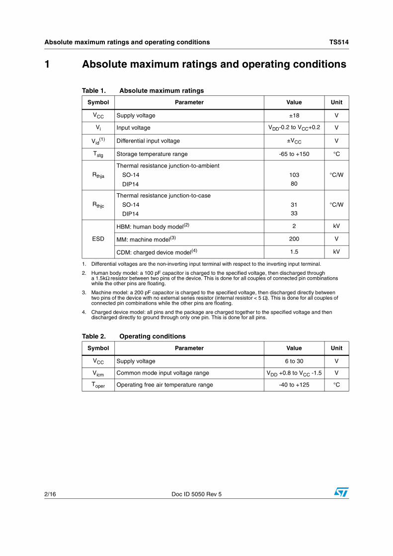
1 Absolute maximum ratings and operating conditions
Table 1. Absolute maximum ratings
Symbol Parameter Value Unit
VCC Supply voltage ±18 V
Vi Input voltage VDD-0.2 to VCC+0.2 V
Vid(1)
1. Differential voltages are the non-inverting input terminal with respect to the inverting input terminal.
Differential input voltage ±VCC V
Tstg Storage temperature range -65 to +150 °C
Rthja
Thermal resistance junction-to-ambient
SO-14
DIP14
103
80
°C/W
Rthjc
Thermal resistance junction-to-case
SO-14
DIP14
31
33
°C/W
ESD
HBM: human body model(2)
2. Human body model: a 100 pF capacitor is charged to the specified voltage, then discharged through a 1.5kΩ resistor between two pins of the device. This is done for all couples of connected pin combinations while the other pins are floating.
2 kV
MM: machine model(3)
3. Machine model: a 200 pF capacitor is charged to the specified voltage, then discharged directly between two pins of the device with no external series resistor (internal resistor < 5 Ω). This is done for all couples of connected pin combinations while the other pins are floating.
200 V
CDM: charged device model(4)
4. Charged device model: all pins and the package are charged together to the specified voltage and then discharged directly to ground through only one pin. This is done for all pins.
1.5 kV
Table 2. Operating conditions
Symbol Parameter Value Unit
VCC Supply voltage 6 to 30 V
Vicm Common mode input voltage range VDD +0.8 to VCC -1.5 V
Toper Operating free air temperature range -40 to +125 °C
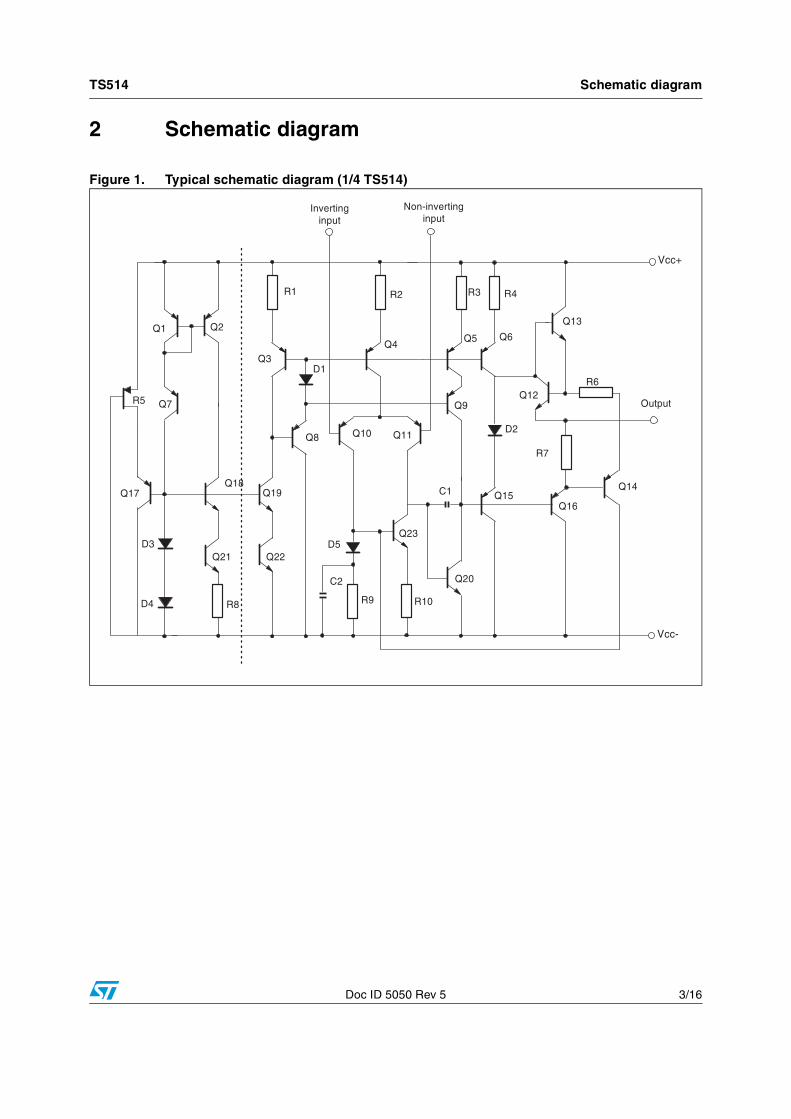
TS514 Schematic diagram
Doc ID 5050 Rev 5 3/16
2 Schematic diagram
Figure 1. Typical schematic diagram (1/4 TS514)
Electrical characteristics TS514
4/16 Doc ID 5050 Rev 5
3 Electrical characteristics
Table 3. Electrical characteristics at VCC = ±15 V, Tamb = 25 °C (unless otherwise specified)
Symbol Parameter Min. Typ. Max. Unit
ICCSupply current (per operator)
at Tmin ≤ Top ≤ Tmax
0.5 0.6
0.75mA
Iib
Input bias current
– at 25 °C
– at Tmin ≤ Top ≤ Tmax
50 150
300
nA
Ri Input resistance, F= 1 kHz 1 MΩ
Vio
Input offset voltage
– at 25 °C
TS514TS514A
– at Tmin ≤ Top ≤ Tmax
TS514TS514A
0.5 2.50.5
41.5
mV
ΔVio Input offset voltage drift at Tmin ≤ Top ≤ Tmax 5 μV/°C
Iio
Input offset current
at 25 °Cat Tmin ≤ Top ≤ Tmax
5 2040
nA
ΔIioInput offset current driftTmin ≤ Top ≤ Tmax 0.08
Ios Output short-circuit current 23 mA
Avd
Large signal voltage gain, RL = 2 kΩ
VCC = ±15 V, at Tmin ≤ Top ≤ Tmax
VCC = ± 4 V90 100
95dB
GBP Gain bandwidth product, F = 100 kHz 1.8 3 MHz
en
Equivalent input noise voltage, F = 1 kHz
Rs = 50 ΩRs = 1 kΩRs = 10 kΩ
81018
15
THDTotal harmonic distortionAv = 20 dB, RL = 2 kΩ, Vo = 2 Vpp, f = 1 kHz 0.03 0.1 %
±Vopp
Output voltage swing, RL = 2 kΩ
VCC = ±15 V, at Tmin ≤ Top ≤ TmaxVCC = ± 4 V
±13±3
V
Vopp Large signal voltage swing, RL = 10 kΩ, F = 10 kHz 28 Vpp
SR Slew rate, unity gain, RL = 2 kΩ 0.8 1.5 V/μs
nA° C-------
nV
Hz-----------

TS514 Electrical characteristics
Doc ID 5050 Rev 5 5/16
CMRCommon mode rejection ratio CMR = 20 log (ΔVic/ΔVio) (Vic = -10 V to 10 V, Vout = VCC/2, RL > 1 MΩ)
90 dB
SVRSupply voltage rejection ratio 20 log (ΔVCC/ΔVio) (VCC = ±5 V to ±15 V, Vout = Vicm = VCC/2)
90 dB
Vo1/Vo2 Channel separation, F = 1 kHz 120 dB
Table 3. Electrical characteristics at VCC = ±15 V, Tamb = 25 °C (unless otherwise specified) (continued)
Symbol Parameter Min. Typ. Max. Unit
Electrical characteristics TS514
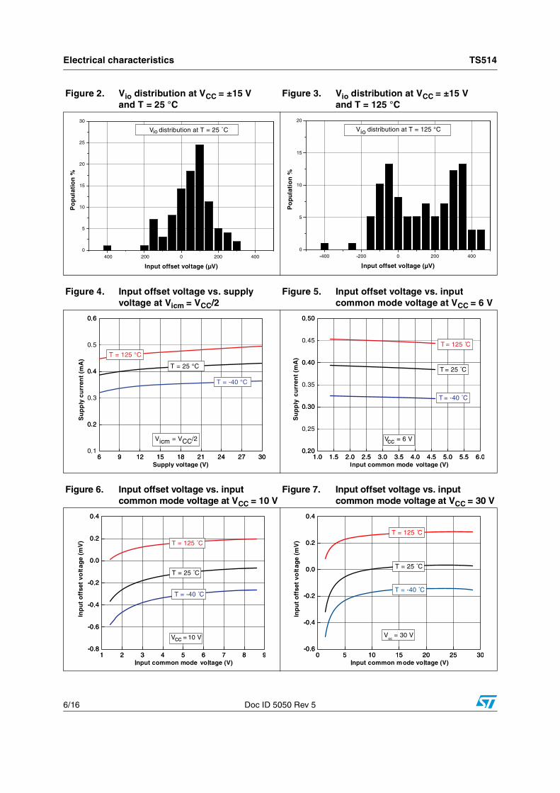
6/16 Doc ID 5050 Rev 5
Figure 2. Vio distribution at VCC = ±15 V and T = 25 °C
Figure 3. Vio distribution at VCC = ±15 V and T = 125 °C
Figure 4. Input offset voltage vs. supply voltage at Vicm = VCC/2
Figure 5. Input offset voltage vs. input common mode voltage at VCC = 6 V
Figure 6. Input offset voltage vs. input common mode voltage at VCC = 10 V
Figure 7. Input offset voltage vs. input common mode voltage at VCC = 30 V

TS514 Electrical characteristics
Doc ID 5050 Rev 5 7/16
Figure 8. Supply current (per operator) vs. supply voltage at Vicm = VCC/2
Figure 9. Supply current (per operator) vs. input common mode voltage at VCC = 6 V
Figure 10. Supply current (per operator) vs. input common mode voltage at VCC = 10 V
Figure 11. Supply current (per operator) vs. input common mode voltage at VCC = 30 V
Figure 12. Output current vs. supply voltage at Vicm = VCC/2
Figure 13. Output current vs. output voltage at VCC = 6 V

Electrical characteristics TS514
8/16 Doc ID 5050 Rev 5
Figure 14. Output current vs. output voltage at VCC = 10 V
Figure 15. Output current vs. output voltage at VCC = 30 V
Figure 16. Voltage gain and phase for different capacitive load at VCC = 6 V, Vicm = 3 V and T = 25 °C
Figure 17. Voltage gain and phase for different capacitive load at VCC = 10 V, Vicm = 5 V and T = 25 °C
Figure 18. Voltage gain and phase for different capacitive load at VCC = 30 V, Vicm = 15 V and T = 25 °C
Figure 19. Frequency response for different capacitive load at VCC = 6 V, Vicm = 3 V and T = 25 °C

TS514 Electrical characteristics
Doc ID 5050 Rev 5 9/16
Figure 20. Frequency response for different capacitive load at VCC= 10 V, Vicm = 5 V and T = 25 °C
Figure 21. Frequency response for different capacitive load at VCC = 30 V, Vicm = 15 V and T = 25 °C
Figure 22. Gain margin vs. output current, at VCC = 6 V, Vicm = 3 V and T = 25 °C
Figure 23. Gain margin vs. output current, at VCC = 10 V, Vicm = 5 V and T = 25 °C
Figure 24. Gain margin vs. output current, at VCC = 30 V, Vicm = 15 V and T = 25 °C
Figure 25. Phase margin vs. output current, at VCC = 6 V, Vicm = 3 V and T = 25 °C
Electrical characteristics TS514
10/16 Doc ID 5050 Rev 5
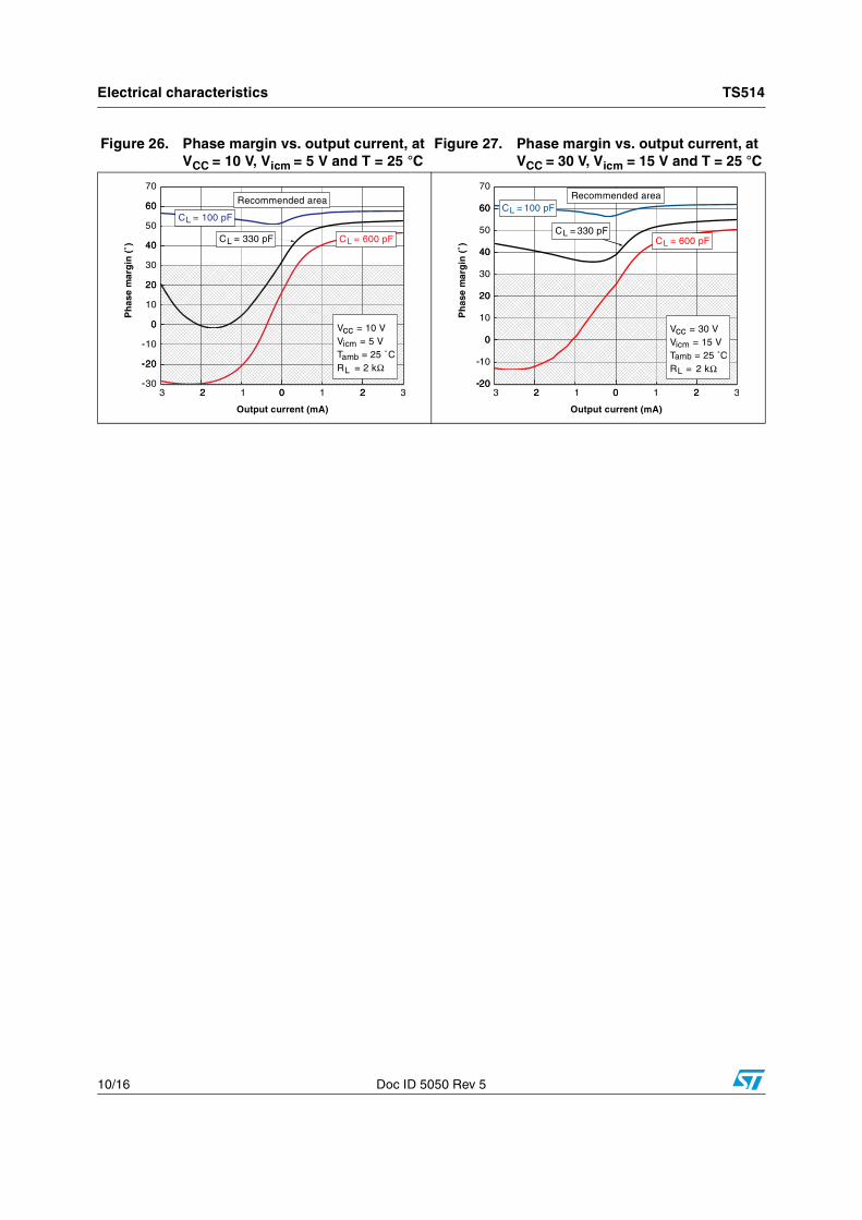
Figure 26. Phase margin vs. output current, at VCC = 10 V, Vicm = 5 V and T = 25 °C
Figure 27. Phase margin vs. output current, at VCC = 30 V, Vicm = 15 V and T = 25 °C
TS514 Package information
Doc ID 5050 Rev 5 11/16
4 Package information
In order to meet environmental requirements, ST offers these devices in different grades of ECOPACK® packages, depending on their level of environmental compliance. ECOPACK specifications, grade definitions and product status are available at: www.st.com. ECOPACK
is an ST trademark.
Package information TS514
12/16 Doc ID 5050 Rev 5
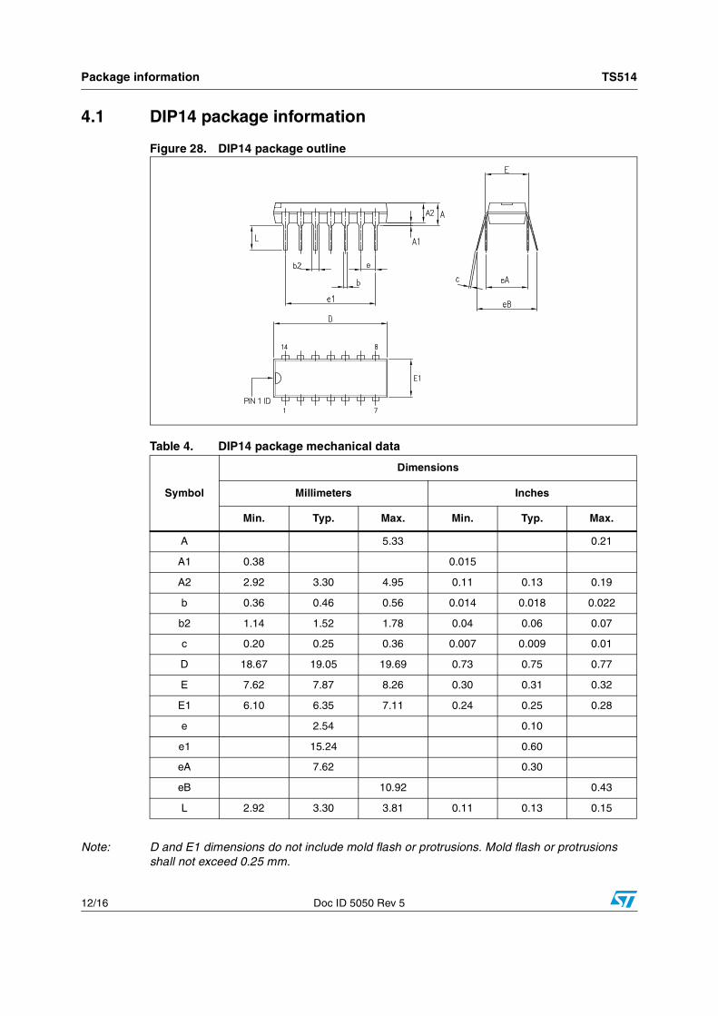
4.1 DIP14 package information
Figure 28. DIP14 package outline
Note: D and E1 dimensions do not include mold flash or protrusions. Mold flash or protrusions shall not exceed 0.25 mm.
Table 4. DIP14 package mechanical data
Symbol
Dimensions
Millimeters Inches
Min. Typ. Max. Min. Typ. Max.
A 5.33 0.21
A1 0.38 0.015
A2 2.92 3.30 4.95 0.11 0.13 0.19
b 0.36 0.46 0.56 0.014 0.018 0.022
b2 1.14 1.52 1.78 0.04 0.06 0.07
c 0.20 0.25 0.36 0.007 0.009 0.01
D 18.67 19.05 19.69 0.73 0.75 0.77
E 7.62 7.87 8.26 0.30 0.31 0.32
E1 6.10 6.35 7.11 0.24 0.25 0.28
e 2.54 0.10
e1 15.24 0.60
eA 7.62 0.30
eB 10.92 0.43
L 2.92 3.30 3.81 0.11 0.13 0.15

TS514 Package information
Doc ID 5050 Rev 5 13/16
4.2 SO-14 package information
Figure 29. SO-14 package outline
Note: D and F dimensions do not include mold flash or protrusions. Mold flash or protrusions must not exceed 0.15 mm.
Table 5. SO-14 package mechanical data
Symbol
Dimensions
Millimeters Inches
Min. Typ. Max. Min. Typ. Max.
A 1.35 1.75 0.05 0.068
A1 0.10 0.25 0.004 0.009
A2 1.10 1.65 0.04 0.06
B 0.33 0.51 0.01 0.02
C 0.19 0.25 0.007 0.009
D 8.55 8.75 0.33 0.34
E 3.80 4.0 0.15 0.15
e 1.27 0.05
H 5.80 6.20 0.22 0.24
h 0.25 0.50 0.009 0.02
L 0.40 1.27 0.015 0.05
k 8° (max.)
ddd 0.10 0.004

Ordering information TS514
14/16 Doc ID 5050 Rev 5
5 Ordering information
Table 6. Order codes
Order codeTemperature
rangePackage Packaging Marking
TS514IN
-40, + 125 °C
DIP14 TubeTS514IN
TS514AIN TS514AIN
TS514ID
TS514IDTSO-14
Tubeor
tape and reel
514I
TS514AID
TS514AIDT514AI

TS514 Revision history
Doc ID 5050 Rev 5 15/16
6 Revision history
Table 7. Document revision history
Date Revision Changes
09-Mar-2001 1 Initial release.
23-Jun-2005 2Automotive grade part references inserted in the datasheet (see Chapter 5: Ordering information on page 14).
30-Sep-2005 3
The following changes were made in this revision.
– An error in the device description was corrected on page 1.
– Chapter 5: Ordering information on page 14 updated with complete list of markings.
– Addition of supplementary data in Table 1: Absolute maximum ratings on page 2.
– Addition of Table 2: Operating conditions on page 2.
– Reorganization of Chapter 4: Package information on page 11.
– Minor grammatical and formatting changes throughout.
24-Oct-2008 4
Added performance AC and DC characteristic curves for VCC=6 V, VCC=10 V and VCC=30 V in Chapter 3: Electrical characteristics.
Modified ICC typ, added parameters over temperature in Table 3.
Deleted old macromodel.
Added Rthjc, Rthja in Table 1.
Corrected Vi and Vid AMR values in Table 1.
Added input common mode range Vicm in Table 2: Operating conditions.
Updated Section 4.1: DIP14 package information and Section 4.2: SO-14 package information.
12-Sep-2012 5
Updated Features (removed “macromodel”).
Updated CMR and SVR test conditions in Table 3.
Updated ECOPACK text in Section 4.
Removed TS514IYD, TS514IYDT, TS514AIYD, and TS514AIYDT order code from Table 6.
Minor corrections throughout document.

TS514
16/16 Doc ID 5050 Rev 5
Please Read Carefully:
Information in this document is provided solely in connection with ST products. STMicroelectronics NV and its subsidiaries (“ST”) reserve theright to make changes, corrections, modifications or improvements, to this document, and the products and services described herein at anytime, without notice.
All ST products are sold pursuant to ST’s terms and conditions of sale.
Purchasers are solely responsible for the choice, selection and use of the ST products and services described herein, and ST assumes noliability whatsoever relating to the choice, selection or use of the ST products and services described herein.
No license, express or implied, by estoppel or otherwise, to any intellectual property rights is granted under this document. If any part of thisdocument refers to any third party products or services it shall not be deemed a license grant by ST for the use of such third party productsor services, or any intellectual property contained therein or considered as a warranty covering the use in any manner whatsoever of suchthird party products or services or any intellectual property contained therein.
UNLESS OTHERWISE SET FORTH IN ST’S TERMS AND CONDITIONS OF SALE ST DISCLAIMS ANY EXPRESS OR IMPLIEDWARRANTY WITH RESPECT TO THE USE AND/OR SALE OF ST PRODUCTS INCLUDING WITHOUT LIMITATION IMPLIEDWARRANTIES OF MERCHANTABILITY, FITNESS FOR A PARTICULAR PURPOSE (AND THEIR EQUIVALENTS UNDER THE LAWSOF ANY JURISDICTION), OR INFRINGEMENT OF ANY PATENT, COPYRIGHT OR OTHER INTELLECTUAL PROPERTY RIGHT.
UNLESS EXPRESSLY APPROVED IN WRITING BY TWO AUTHORIZED ST REPRESENTATIVES, ST PRODUCTS ARE NOTRECOMMENDED, AUTHORIZED OR WARRANTED FOR USE IN MILITARY, AIR CRAFT, SPACE, LIFE SAVING, OR LIFE SUSTAININGAPPLICATIONS, NOR IN PRODUCTS OR SYSTEMS WHERE FAILURE OR MALFUNCTION MAY RESULT IN PERSONAL INJURY,DEATH, OR SEVERE PROPERTY OR ENVIRONMENTAL DAMAGE. ST PRODUCTS WHICH ARE NOT SPECIFIED AS "AUTOMOTIVEGRADE" MAY ONLY BE USED IN AUTOMOTIVE APPLICATIONS AT USER’S OWN RISK.
Resale of ST products with provisions different from the statements and/or technical features set forth in this document shall immediately voidany warranty granted by ST for the ST product or service described herein and shall not create or extend in any manner whatsoever, anyliability of ST.
ST and the ST logo are trademarks or registered trademarks of ST in various countries.
Information in this document supersedes and replaces all information previously supplied.
The ST logo is a registered trademark of STMicroelectronics. All other names are the property of their respective owners.
© 2012 STMicroelectronics - All rights reserved
STMicroelectronics group of companies
Australia - Belgium - Brazil - Canada - China - Czech Republic - Finland - France - Germany - Hong Kong - India - Israel - Italy - Japan - Malaysia - Malta - Morocco - Philippines - Singapore - Spain - Sweden - Switzerland - United Kingdom - United States of America
www.st.com