Quad, Low-Power, Current-Feedback Operational Amplifier ...
34
www.ti.com OPA4684 ® OPA4684 PRODUCTION DATA information is current as of publication date. Products conform to specifications per the terms of Texas Instruments standard warranty. Production processing does not necessarily include testing of all parameters. OPA4684 www.ti.com Copyright © 2002-2008, Texas Instruments Incorporated Please be aware that an important notice concerning availability, standard warranty, and use in critical applications of Texas Instruments semiconductor products and disclaimers thereto appears at the end of this data sheet. SBOS240G – JUNE 2002 – REVISED JULY 2008 Quad, Low-Power, Current-Feedback Operational Amplifier FEATURES ● MINIMAL BANDWIDTH CHANGE VERSUS GAIN ● 170MHz BANDWIDTH AT G = +2 ● > 120MHz BANDWIDTH TO GAIN > +10 ● LOW DISTORTION: < –78dBc at 5MHz ● HIGH OUTPUT CURRENT: 120mA ● SINGLE +5V TO +12V SUPPLY OPERATION ● DUAL ± 2.5 TO ±6.0V SUPPLY OPERATION ● LOW SUPPLY CURRENT: 1.7mA/ch DESCRIPTION The OPA4684 provides a new level of performance in low- power, wideband, current-feedback (CFB) amplifiers. This CFB PLUS amplifier is among the first to use an internally closed-loop input buffer stage that enhances performance significantly over earlier low-power CFB amplifiers. This new architecture provides many of the benefits of a more ideal CFB amplifier while retaining the benefits of very low power operation. The closed-loop input stage buffer gives a very low and linearized impedance path at the inverting input to sense the feedback error current. This improved inverting input impedance retains exceptional bandwidth to much higher gains and improves harmonic distortion over earlier solutions limited by inverting input linearity. Beyond simple high-gain applications, the OPA4684 CFB PLUS amplifier per- mits the gain setting element to be set with considerable APPLICATIONS ● LOW-POWER BROADCAST VIDEO DRIVERS ● EQUALIZING FILTERS ● SAW FILTER HIGH-GAIN POST AMPLIFIERS ● MULTICHANNEL SUMMING AMPLIFIERS ● WIDEBAND DIFFERENTIAL CHANNELS ● ANALOG-TO-DIGITAL CONVERTERS INPUT DRIVERS ● MULTIPLE POLE ACTIVE FILTERS ● OPA4658 LOW-POWER UPGRADE freedom from amplifier bandwidth interaction. This allows frequency response peaking elements to be added, multiple input inverting summing circuits to have greater bandwidth, and low-power line drivers to meet the demanding require- ments of studio cameras and broadcast video. The output capability of the OPA4684 also sets a new mark in performance for low-power current-feedback amplifiers. Delivering a full ±4V PP swing on ±5V supplies, the OPA4684 also has the output current to support > ±3V swing into 50Ω. This minimal output headroom requirement is complemented by a similar 1.2V input stage headroom giving exceptional capability for single +5V operation. The OPA4684’s low 6.8mA supply current is precisely trimmed at 25°C. This trim, along with low shift over temperature and supply voltage, gives a very robust design over a wide range of operating conditions. (patented design) V+ V O V– I ERR R G R F Z (S) I ERR + Low-Power Amplifier 1 of 4 Channels 6 3 0 –3 –6 –9 –12 –15 –18 –21 –24 Normalized Gain (3dB/div) R F = 800Ω G = 100 G = 50 G = 20 G = 10 G = 2 G = 1 10 100 200 BW (MHz) vs GAIN G = 5 MHz All trademarks are the property of their respective owners.
Transcript of Quad, Low-Power, Current-Feedback Operational Amplifier ...

www.ti.com
OPA4684
®OPA4684
PRODUCTION DATA information is current as of publication date.Products conform to specifications per the terms of Texas Instrumentsstandard warranty. Production processing does not necessarily includetesting of all parameters.
OPA4684
www.ti.com
Copyright © 2002-2008, Texas Instruments Incorporated
Please be aware that an important notice concerning availability, standard warranty, and use in critical applications ofTexas Instruments semiconductor products and disclaimers thereto appears at the end of this data sheet.
SBOS240G – JUNE 2002 – REVISED JULY 2008
Quad, Low-Power, Current-FeedbackOperational Amplifier
FEATURES MINIMAL BANDWIDTH CHANGE VERSUS GAIN 170MHz BANDWIDTH AT G = +2 > 120MHz BANDWIDTH TO GAIN > +10 LOW DISTORTION: < –78dBc at 5MHz HIGH OUTPUT CURRENT: 120mA SINGLE +5V TO +12V SUPPLY OPERATION DUAL ±2.5 TO ±6.0V SUPPLY OPERATION LOW SUPPLY CURRENT: 1.7mA/ch
DESCRIPTIONThe OPA4684 provides a new level of performance in low-power, wideband, current-feedback (CFB) amplifiers. ThisCFBPLUS amplifier is among the first to use an internallyclosed-loop input buffer stage that enhances performancesignificantly over earlier low-power CFB amplifiers. This newarchitecture provides many of the benefits of a more idealCFB amplifier while retaining the benefits of very low poweroperation. The closed-loop input stage buffer gives a verylow and linearized impedance path at the inverting input tosense the feedback error current. This improved invertinginput impedance retains exceptional bandwidth to muchhigher gains and improves harmonic distortion over earliersolutions limited by inverting input linearity. Beyond simplehigh-gain applications, the OPA4684 CFBPLUS amplifier per-mits the gain setting element to be set with considerable
APPLICATIONS LOW-POWER BROADCAST VIDEO DRIVERS EQUALIZING FILTERS SAW FILTER HIGH-GAIN POST AMPLIFIERS MULTICHANNEL SUMMING AMPLIFIERS WIDEBAND DIFFERENTIAL CHANNELS ANALOG-TO-DIGITAL CONVERTERS INPUT
DRIVERS MULTIPLE POLE ACTIVE FILTERS OPA4658 LOW-POWER UPGRADE
freedom from amplifier bandwidth interaction. This allowsfrequency response peaking elements to be added, multipleinput inverting summing circuits to have greater bandwidth,and low-power line drivers to meet the demanding require-ments of studio cameras and broadcast video.
The output capability of the OPA4684 also sets a new markin performance for low-power current-feedback amplifiers.Delivering a full ±4VPP swing on ±5V supplies, the OPA4684also has the output current to support > ±3V swing into 50Ω.This minimal output headroom requirement is complementedby a similar 1.2V input stage headroom giving exceptionalcapability for single +5V operation.The OPA4684’s low 6.8mA supply current is precisely trimmedat 25°C. This trim, along with low shift over temperature andsupply voltage, gives a very robust design over a wide rangeof operating conditions.
(patented design)
V+
VO
V–
IERR
RG
RF
Z(S) IERR
+
Low-Power Amplifier
1 of 4 Channels6
3
0
–3
–6
–9
–12
–15
–18
–21
–24
Nor
mal
ized
Gai
n (3
dB/d
iv)
RF = 800Ω G = 100G = 50
G = 20
G = 10
G = 2
G = 1
10 100 200
BW (MHz) vs GAIN
G = 5
MHz
All trademarks are the property of their respective owners.

OPA46842SBOS240Gwww.ti.com
ABSOLUTE MAXIMUM RATINGS(1)
Power Supply ............................................................................... ±6.5VDC
Internal Power Dissipation ................................. See Thermal InformationDifferential Input Voltage .................................................................. ±1.2VInput Voltage Range ............................................................................ ±VS
Storage Temperature Range: ID, IDBV ......................... –65°C to +125°CLead Temperature (soldering, 10s) .............................................. +300°CJunction Temperature (TJ ) ........................................................... +150°CESD Rating: HBM ............................................................................ 2000V
CDM ........................................................................... 1500V
NOTE: (1) Stresses above these ratings may cause permanent damage.Exposure to absolute maximum conditions for extended periods may degradedevice reliability.
SPECIFIEDPACKAGE TEMPERATURE PACKAGE ORDERING TRANSPORT
PRODUCT PACKAGE-LEAD DESIGNATOR RANGE MARKING NUMBER MEDIA, QUANTITY
OPA4684 SO-14 D –40°C to +85°C OPA4684 OPA4684ID Rails, 58
" " " " " OPA4684IDR Tape and Reel, 2500
OPA4684 TSSOP-14 PW –40°C to +85°C OPA4684 OPA4684IPWT Tape and Reel, 250
" " " " " OPA4684IPWR Tape and Reel, 2500
PACKAGE/ORDERING INFORMATION(1)
ELECTROSTATICDISCHARGE SENSITIVITY
This integrated circuit can be damaged by ESD. TexasInstruments recommends that all integrated circuits be handledwith appropriate precautions. Failure to observe proper han-dling and installation procedures can cause damage.
ESD damage can range from subtle performance degrada-tion to complete device failure. Precision integrated circuitsmay be more susceptible to damage because very smallparametric changes could cause the device not to meet itspublished specifications.
PIN CONFIGURATION
OPA4684 RELATED PRODUCTS
SINGLES DUALS TRIPLES FEATURES
OPA683 OPA2683 — Very Low-Power CFBPLUS
OPA684 OPA2684 OPA3684 Low-Power CFBPLUS
OPA691 OPA2691 OPA3691 High Slew Rate CFBOPA695 — — > 500MHz CFB
Top View SO, TSSOP
NOTE: (1) For the most current package and ordering information, see the Package Option Addendum located at the end of this document, or see the TI web siteat www.ti.com.
1
2
3
4
5
6
7
+V
+Input B
–Input B
Output B
+Input A
–Input A
Output A
+Input C
–Input C
Output C
+Input D
–Input D
Output D
–V
14
13
12
11
10
9
8
OPA4684
DA
B C

OPA4684 3SBOS240G www.ti.com
OPA4684ID, IPW
0°C to –40°C to MIN/ TESTPARAMETER CONDITIONS +25°C +25°C(1) 70°C(2) +85°C(2) UNITS MAX LEVEL(3)
TYP MIN/MAX OVER TEMPERATURE
ELECTRICAL CHARACTERISTICS: VS = ±5VBoldface limits are tested at +25°C.RF = 800Ω, RL = 100Ω, and G = +2, (see Figure 1 for AC performance only), unless otherwise noted.
AC PERFORMANCE (see Figure 1)Small-Signal Bandwidth (VO = 0.5VPP) G = +1, RF = 800Ω 250 MHz typ C
G = +2, RF = 800Ω 170 120 118 117 MHz min BG = +5, RF = 800Ω 138 MHz typ C
G = +10, RF = 800Ω 120 MHz typ CG = +20, RF = 800Ω 95 MHz typ C
Bandwidth for 0.1dB Gain Flatness G = +2, VO = 0.5VPP, RF = 800Ω 19 16 14 14 MHz min BPeaking at a Gain of +1 RF = 800Ω, VO = 0.5VPP 1.4 4.8 5.9 6.3 dB max BLarge-Signal Bandwidth G = +2, VO = 4VPP 90 MHz typ CSlew Rate G = –1, VO = 4V Step 780 675 650 575 V/µs min B
G = +2, VO = 4V Step 750 680 660 650 V/µs min BRise-and-Fall Time G = +2, VO = 0.5V Step 3 ns typ C
G = +2, VO = 4VStep 6.8 ns typ CHarmonic Distortion G = +2, f = 5MHz, VO = 2VPP2nd-Harmonic RL = 100Ω –67 –59 –59 –58 dBc max B
RL ≥ 1kΩ –82 –66 –65 –65 dBc max B3rd-Harmonic RL = 100Ω –70 –66 –65 –65 dBc max B
RL ≥ 1kΩ –84 –82 –81 –81 dBc max BInput Voltage Noise f > 1MHz 3.7 4.1 4.2 4.4 nV/√Hz max BNoninverting Input Current Noise f > 1MHz 9.4 11 12 12.5 pA/√Hz max BInverting Input Current Noise f > 1MHz 17 18 18.5 19 pA/√Hz max BDifferential Gain G = +2, NTSC, VO = 1.4VPP, RL = 150Ω 0.04 % typ CDifferential Phase G = +2, NTSC, VO = 1.4VPP, RL = 150Ω 0.02 deg typ CAll Hostile Crosstalk, Input-Referred 3 Channels Driven at 5MHz, 1VPP –52 dB typ C
4th Channel Measured
DC PERFORMANCE(4)
Open-Loop Transimpedance Gain (ZOL) VO = 0V, RL = 1kΩ 355 160 155 153 kΩ min AInput Offset Voltage VCM = 0V ±1.5 ±4.0 ±4.6 ±4.8 mV max AAverage Offset Voltage Drift VCM = 0V ±12 ±12 µV/°C max BNoninverting Input Bias Current VCM = 0V ±5.0 ±13 ±14.5 ±15 µA max AAverage Noninverting Input Bias Current Drift VCM = 0V ±25 ±30 nA/°C max BInverting Input Bias Current VCM = 0V ±5.0 ±17 ±18.5 ±19.5 µA max AAverage Inverting Input Bias Current Drift VCM = 0V ±35 ±40 nA°/C max B
INPUTCommon-Mode Input Range(5) (CMIR) ±3.75 ±3.65 ±3.65 ±3.6 V min ACommon-Mode Rejection Ratio (CMRR) VCM = 0V 60 53 52 52 dB min ANoninverting Input Impedance 50 || 2 kΩ || pF typ CInverting Input Resistance (RI) Open-Loop, DC 4.0 Ω typ C
OUTPUTVoltage Output Swing 1kΩ Load ±4.1 ±3.9 ±3.9 ±3.8 V min ACurrent Output, Sourcing VO = 0 160 120 115 110 mA min ACurrent Output, Sinking VO = 0 –120 –100 –95 –90 mA min AClosed-Loop Output Impedance G = +2, f = 100kHz 0.006 Ω typ C
POWER SUPPLYSpecified Operating Voltage ±5 V typ CMaximum Operating Voltage Range ±6 ±6 ±6 V max AMinimum Operating Voltage Range ±1.4 V min CMax Quiescent Current VS = ±5V/per Channel 1.7 1.8 1.9 1.95 mA max AMin Quiescent Current VS = ±5V/per Channel 1.7 1.6 1.55 1.45 mA min APower-Supply Rejection Ratio (–PSRR) Input-Referred 60 54 53 53 dB typ A
TEMPERATURE RANGESpecification: ID, IPW –40 to +85 °C typ CThermal Resistance, θJA Junction-to-Ambient
D SO-14 100 °C/W typ CPW TSSOP-14 110 °C/W typ C
NOTES: (1) Junction temperature = ambient for +25°C tested specifications. (2) Junction temperature = ambient at low temperature limit, junction temperature = ambient+7°C at high temperature limit for over temperature tested specifications. (3) Test levels: (A) 100% tested at +25°C. Over temperature limits by characterization andsimulation. (B) Limits set by characterization and simulation. (C) Typical value only for information. (4) Current is considered positive out-of-node. VCM is the inputcommon-mode voltage. (5) Tested < 3dB below minimum specified CMR at ± CMIR limits.

OPA46844SBOS240Gwww.ti.com
OPA4684ID, IPW
0°C to –40°C to MIN/ TESTPARAMETER CONDITIONS +25°C +25°C(1) 70°C(2) +85°C(2) UNITS MAX LEVEL(3)
TYP MIN/MAX OVER TEMPERATURE
ELECTRICAL CHARACTERISTICS: VS = +5VBoldface limits are tested at +25°C.RF = 1kΩ, RL = 100Ω to VS/2, and G = +2, (see Figure 3 for AC performance only), unless otherwise noted.
AC PERFORMANCE (see Figure 3)Small-Signal Bandwidth (VO = 0.5VPP) G = +1, RF = 1.3kΩ 140 MHz typ C
G = +2, RF = 1.3kΩ 110 86 85 82 MHz min BG = +5, RF = 1.3kΩ 100 MHz min CG = +10, RF = 1.3kΩ 90 MHz typ CG = +20, RF = 1.3kΩ 75 MHz typ C
Bandwidth for 0.1dB Gain Flatness G = +2, VO < 0.5Vp-p, RF = 1.3kΩ 21 12 11 10 MHz min BPeaking at a Gain of +1 RF = 1.3kΩ, VO < 0.5VPP 0.5 2.6 3.4 3.7 dB max BLarge-Signal Bandwidth G = 2, VO = 2VPP 86 MHz typ CSlew Rate G = 2, VO = 2V Step 300 300 290 280 V/µs min B
G = 2, VO = 0.5V Step 4.3 ns typ CRise-and-Fall Time G = 2, VO = 2VStep 5.3 ns typ CHarmonic Distortion G = 2, f = 5MHz, VO = 2VPP2nd-Harmonic RL = 100Ω to VS/2 –65 –60 –59 –59 dBc max B
RL ≥ 1kΩ to VS/2 –84 –62 –61 –61 dBc max B3rd-Harmonic RL = 100Ω to VS/2 –65 –64 –63 –63 dBc max B
RL ≥ 1kΩ to VS/2 –74 –70 –70 –69 dBc max BInput Voltage Noise f > 1MHz 3.7 4.1 4.2 4.4 nV/√Hz max BNoninverting Input Current Noise f > 1MHz 9.4 11 12 12.5 pA/√Hz max BInverting Input Current Noise f > 1MHz 17 18 18.5 19 pA/√Hz max BDifferential Gain G = +2, NTSC, VO = 1.4VPP, RL = 150Ω 0.04 % typ CDifferential Phase G = +2, NTSC, VO = 1.4VPP, RL = 150Ω 0.07 deg typ CAll Hostile X-Talk, Input-Referred 3-Channels Driven at 5MHz, 1VPP –52 dB typ C
4th Channel Measured
DC PERFORMANCE(4)
Open-Loop Transimpedance Gain (ZOL) VO = VS/2, RL = 1kΩ to VS/2 355 160 155 153 kΩ min AInput Offset Voltage VCM = VS/2 ±1.0 ±3.5 ±4.1 ±4.3 mV max AAverage Offset Voltage Drift VCM = VS/2 ±12 ±12 µV/°C max BNoninverting Input Bias Current VCM = VS/2 ±5 ±13 ±14.5 ±15 µA max AAverage Noninverting Input Bias Current Drift VCM = VS/2 ±25 ±30 nA/°C max BInverting Input Bias Current VCM = VS/2 ±5 ±13 ±14.5 ±16 µA max AAverage Inverting Input Bias Current Drift VCM = VS/2 ±25 ±30 nA°/C max B
INPUTLeast Positive Input Voltage(5) 1.25 1.32 1.35 1.38 V max AMost Positive Input Voltage(5) 3.75 3.68 3.65 3.62 V min ACommon-Mode Refection Ratio (CMRR) VCM = VS/2 58 51 50 50 dB min ANoninverting Input Impedance 50 || 1 kΩ || pF typ CInverting Input Resistance (RI) Open-Loop 5 Ω typ C
OUTPUTMost Positive Output Voltage RL = 1kΩ to VS/2 4.10 3.9 3.9 3.8 V min ALeast Positive Output Voltage RL = 1kΩ to VS/2 0.9 1.1 1.1 1.2 V max ACurrent Output, Sourcing VO = VS/2 80 65 60 55 mA min ACurrent Output, Sinking VO = VS/2 70 55 50 45 mA min AClosed-Loop Output Impedance G = +2, f = 100kHz 0.006 Ω typ C
POWER SUPPLYSpecified Single-Supply Operating Voltage 5 V typ CMax Single-Supply Operating Voltage 12 12 12 V max AMin Single-Supply Operating Voltage 2.8 V min CMax Quiescent Current VS = +5V/per Channel 1.45 1.55 1.55 1.55 mA max AMin Quiescent Current VS = +5V/per Channel 1.45 1.30 1.20 1.15 mA min APower-Supply Rejection Ratio (+PSRR) Input-Referred 58 dB typ C
TEMPERATURE RANGESpecification: ID, IPW –40 to +85 °C typ CThermal Resistance, θJA Junction-to-Ambient
D SO-14 100 °C/W typ CPW TSSOP-14 110 °C/W typ C
NOTES: (1) Junction temperature = ambient for +25°C tested specifications. (2) Junction temperature = ambient at low temperature limit, junction temperature = ambient+3°C at high temperature limit for over temperature tested specifications. (3) Test levels: (A) 100% tested at +25°C. Over temperature limits by characterization andsimulation. (B) Limits set by characterization and simulation. (C) Typical value only for information. (4) Current is considered positive out-of-node. VCM is the inputcommon-mode voltage. (5) Tested < 3dB below minimum specified CMR at ± CMIR limits.
OPA4684 5SBOS240G www.ti.com
TYPICAL CHARACTERISTICS: VS = ±5VAt TA = +25°C, G = +2, RF = 800Ω, and RL = 100Ω, unless otherwise noted.
NONINVERTING PULSE RESPONSE
Time (10ns/div)
Out
put V
olta
ge (
200m
V/d
iv)
Out
put V
olta
ge (
400m
V/d
iv)
0.8
0.6
0.4
0.2
0
–0.2
–0.4
–0.6
–0.8
1.6
1.2
0.8
0.4
0
–0.4
–0.8
–1.2
–1.6
Large-Signal Right Scale
Small-Signal Left Scale
See Figure 1
G = +2
INVERTING PULSE RESPONSE
Time (10ns/div)
Out
put V
olta
ge (
200m
V/d
iv)
Out
put V
olta
ge (
400m
V/d
iv)
0.8
0.6
0.4
0.2
0
–0.2
–0.4
–0.6
–0.8
1.6
1.2
0.8
0.4
0
–0.4
–0.8
–1.2
–1.6
Large-Signal Right Scale
Small-Signal Left Scale
See Figure 2
G = –1
3
0
–3
–6
–9
–12
Frequency (MHz)
1 20010 100
INVERTING SMALL-SIGNAL FREQUENCY RESPONSE
Nor
mal
ized
Gai
n (3
dB/d
iv)
VO = 0.5VPPRF = 800Ω
See Figure 2
G = –1
G = –10G = –16
G = –5G = –2
9
6
3
0
–3
Frequency (MHz)
1 20010 100
NONINVERTING LARGE-SIGNALFREQUENCY RESPONSE
Gai
n (d
B)
G = +2RL = 100Ω
See Figure 1
VO = 1VPP
VO = 0.5VPP
VO = 5VPP
VO = 2VPP
3
0
–3
–6
–9
–12
Frequency (MHz)
1 20010 100
INVERTING LARGE-SIGNAL FREQUENCY RESPONSE
Gai
n (d
B)
G = –1RL = 100Ω VO = 0.5VPP
See Figure 2
2VPP
1VPP
5VPP
6
3
0
–3
–6
–9
–12
–15
–18
Frequency (MHz)
1 20010 100
NONINVERTING SMALL-SIGNALFREQUENCY RESPONSE
Nor
mal
ized
Gai
n (3
dB/d
iv)
VO = 0.5VPPRF = 800Ω
See Figure 1
G = 1G = 2
G = 50
G = 20
G = 10G = 5
G = 100
OPA46846SBOS240Gwww.ti.com
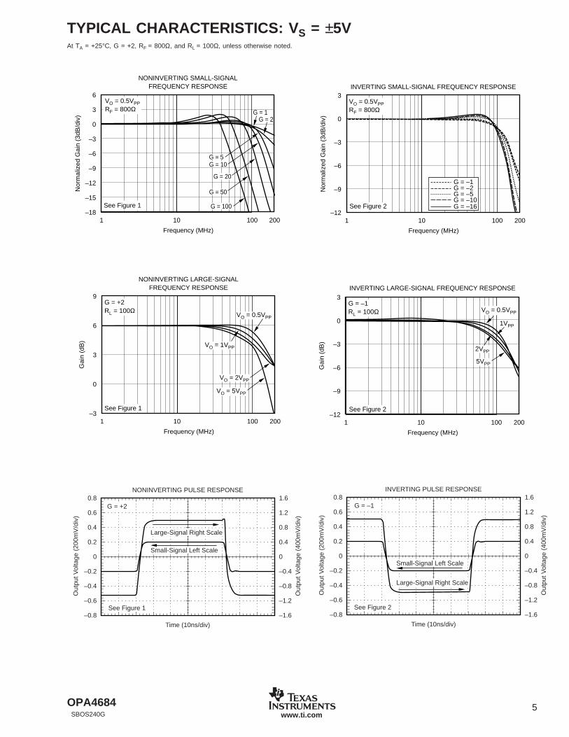
TYPICAL CHARACTERISTICS: VS = ±5V (Cont.)At TA = +25°C, G = +2, RF = 800Ω, and RL = 100Ω, unless otherwise noted.
HARMONIC DISTORTION vs LOAD RESISTANCE
100 1kLoad Resistance (Ω)
Har
mon
ic D
isto
rtio
n (d
Bc)
–50
–55
–60
–65
–70
–75
–80
–85
–90
VO = 2VPPf = 5MHzG = +2
See Figure 1
2nd-Harmonic
3rd-Harmonic
–50
–60
–70
–80
–90
Frequency (MHz)
0.1 201 10
HARMONIC DISTORTION vs FREQUENCY
Har
mon
ic D
isto
rtio
n (d
Bc)
VO = 2VPPRL = 100Ω
See Figure 1
2nd-Harmonic
3rd-Harmonic
HARMONIC DISTORTION vs OUTPUT VOLTAGE
0.5 1 5Output Voltage (VPP)
Har
mon
ic D
isto
rtio
n (d
Bc)
–50
–60
–70
–80
–90
f = 5MHzRL = 100Ω
2nd-Harmonic
3rd-Harmonic
5MHz HARMONIC DISTORTION vs SUPPLY VOLTAGE
2.5 3.0 3.5 4.0 4.5 5.0 5.5 6.0Supply Voltage (±V)
Har
mon
ic D
isto
rtio
n (d
Bc)
–50
–60
–70
–80
–90
VO = 2VPPRL = 100Ω
2nd-Harmonic
3rd-Harmonic
HARMONIC DISTORTION vs NONINVERTING GAIN
Gain (V/V)
Har
mon
ic D
isto
rtio
n (d
Bc)
1 10 20
–50
–55
–60
–65
–70
–75
–80
–85
–90
2nd-Harmonic
3rd-Harmonic
HARMONIC DISTORTION vs INVERTING GAIN
1 10 20Inverting Gain (V/V)
Har
mon
ic D
isto
rtio
n (d
Bc)
–50
–55
–60
–65
–70
–75
–80
–85
–90
2nd-Harmonic
3rd-Harmonic

OPA4684 7SBOS240G www.ti.com
TYPICAL CHARACTERISTICS: VS = ±5V (Cont.)At TA = +25°C, G = +2, RF = 800Ω, and RL = 100Ω, unless otherwise noted.
100
10
1
Frequency (Hz)
100 10M1k 10k 100k 1M
INPUT VOLTAGE AND CURRENT NOISE DENSITY
Vol
tage
Noi
se (
nV/√
Hz)
Cur
rent
Noi
se (
pA/√
Hz)
Noninverting Current Noise9.4pA/√Hz
Voltage Noise3.7nV/√Hz
Inverting Current Noise17pA/√Hz
2-TONE, 3RD-ORDER INTERMODULATION DISTORTION
–8 –7 –6 –5 –4 –3 –2 –1 4 53210 6 7 8Power at Load (each tone, dBm)
3rd-
Ord
er S
purio
us L
evel
(dB
c)
–50
–60
–70
–80
–90
50Ω
+5V
–5V
50Ω
50Ω
PI
PO
800Ω
800Ω
OPA4684
20MHz
10MHz
5MHz
1MHz
50
40
30
20
10
0
CLOAD (pF)
1 10010
RS vs CLOAD
RS (
Ω)
0.5dB Peaking
CMRR and PSRR vs FREQUENCY
100 1k 10k 100k 1M 10M 100MFrequency (Hz)
Com
mon
-Mod
e R
ejec
tion
Rat
io (
dB)
Pow
er-S
uppl
y R
ejec
tion
Rat
io (
dB)
70
60
50
40
30
20
10
0
CMRR
+PSRR
–PSRR
OPEN-LOOP TRANSIMPEDANCE GAIN AND PHASE
100 1k 10k 100k 1M 10M 100M 1GFrequency (Hz)
Ope
n-Lo
op T
rans
impe
danc
e G
ain
(dB
Ω) 120
100
80
60
40
20
0
Ope
n-Lo
op P
hase
(°)
0
–30
–60
–90
–120
–150
–180
20log (ZOL)
∠ ZOL
9
6
3
0
–3
–6
Frequency (MHz)
1 30010 100
SMALL-SIGNAL BANDWIDTH vs CLOAD
Nor
mal
ized
Gai
n (d
B)
5pF
800Ω
800Ω
1kΩ
OPA4684
RS VO
+5V
–5V
50Ω
CL
VI
12pF
100pF
50pF
75pF
20pF
33pF

OPA46848SBOS240Gwww.ti.com
TYPICAL CHARACTERISTICS: VS = ±5V (Cont.)At TA = +25°C, G = +2, RF = 800Ω, and RL = 100Ω, unless otherwise noted.
0.10
0.09
0.08
0.07
0.06
0.05
0.04
0.03
0.02
0.01
0
Number of 150Ω Video Loads
1 42 3
COMPOSITE VIDEO DIFFERENTIAL GAIN/PHASE
Diff
eren
tial G
ain
(%)
Diff
eren
tial P
hase
(°)
Gain = +2NTSC, Positive Video
dG
dP
1W PowerLimit
OUTPUT CURRENT AND VOLTAGE LIMITATIONS
–150 –100 –50 0 50 100 150IO (MA)
VO (
V)
5
4
3
2
1
0
–1
–2
–3
–4
–5
EachChannel
R L =
100
Ω
R L = 50
Ω
R L =
500Ω
1W PowerLimit
TYPICAL DC DRIFT OVER AMBIENT TEMPERATURE
–50 –25 0 25 50 75 100 125
Ambient Temperature (°C)
Inpu
t Bia
s C
urre
nts
(µA
)an
d O
ffset
Vol
tage
(m
V)
4
3
2
1
0
–1
–2
–3
–4
Input Offset VoltageNoninverting Input Bias Current
Inverting Input Bias Current
SUPPLY AND OUTPUT CURRENTvs AMBIENT TEMPERATURE
–25 0 25 50 75 100 125Ambient Temperature (°C)
Out
put C
urre
nt (
mA
)200
175
150
125
100
Sup
ply
Cur
rent
(m
A)
Sourcing Output Current
Sinking Output Current
Supply Current
7.6
7.2
6.8
6.4
6.0
SETTLING TIME
0 10 20 30 40 50 60Time (ns)
% E
rror
to F
inal
Val
ue
0.05
0.04
0.03
0.02
0.01
0
–0.01
–0.02
–0.03
–0.04
–0.05
2V StepSee Figure 1
ALL HOSTILE CROSSTALK
Frequency (MHz)
1010.1 100
Cro
ssta
lk,
Inpu
t-R
efer
red
(dB
)
–20
–25
–30
–35
–40
–45
–50
–55
–60
–65
–70
1VPP Output3-Channels, 100Ω Load

OPA4684 9SBOS240G www.ti.com
TYPICAL CHARACTERISTICS: VS = ±5V (Cont.)At TA = +25°C, G = +2, RF = 800Ω, and RL = 100Ω, unless otherwise noted.
NONINVERTING OVERDRIVE RECOVERY
Time (100ns/div)
Inpu
t Vol
tage
(0.
8V/d
iv)
Out
put V
olta
ge (
1.6V
/div
)
4.0
3.2
2.4
1.6
0.8
0
–0.8
–1.6
–2.4
–3.2
–4.0
8.0
6.4
4.8
3.2
1.6
0
–1.6
–3.2
–4.8
–6.4
–8.0
See Figure 1
Input VoltageLeft Scale
Output VoltageRight Scale
INVERTING OVERDRIVE RECOVERY
Time (100ns/div)
Inpu
t Vol
tage
(1.
6V/d
iv)
Out
put V
olta
ge (
1.6V
/div
)
8.0
6.4
4.8
3.2
1.6
0
–1.6
–3.2
–4.8
–6.4
–8.0
8.0
6.4
4.8
3.2
1.6
0
–1.6
–3.2
–4.8
–6.4
–8.0
See Figure 2Input Voltage
Left Scale
Output VoltageRight Scale
INPUT AND OUTPUT RANGE vs SUPPLY VOLTAGE
Supply Voltage (±V)
± 4± 3± 2 ± 5 ± 6
Inpu
t and
Out
put V
olta
ge R
ange
6
5
4
3
2
1
0
–1
–2
–3
–4
–5
–6
InputVoltageRange
OutputVoltageRange
CLOSED-LOOP OUTPUT IMPEDANCE vs FREQUENCY
Frequency (Hz)
100k 1M1k 10k100 10M 100M
Out
put I
mpe
danc
e (Ω
)
100
10
1
0.01
0.001
800Ω ZO
800Ω
1/4OPA4684
OPA468410SBOS240Gwww.ti.com
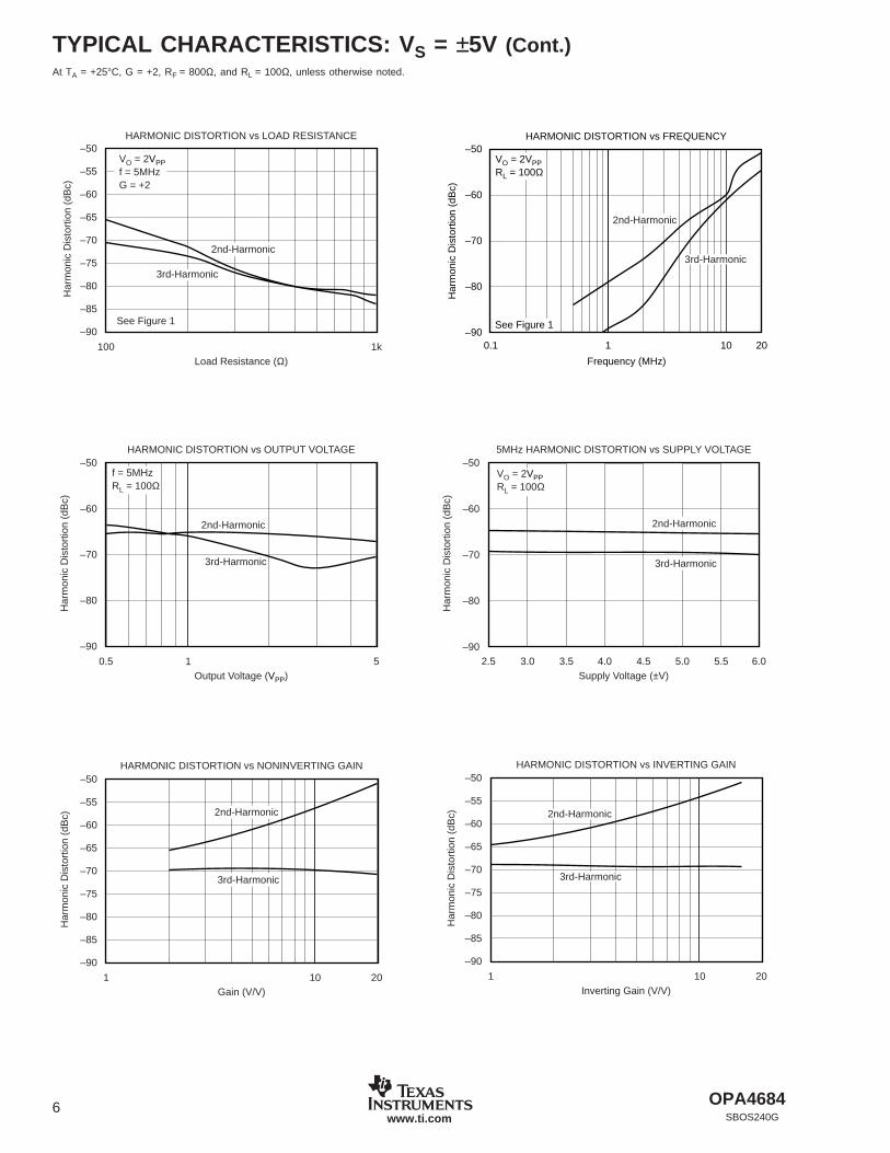
TYPICAL CHARACTERISTICS: VS = +5VAt TA = +25°C, G = +2, RF = 1kΩ, and RL = 100Ω to VS/2, unless otherwise noted.
6
3
0
–3
–6
–9
–12
–15
–18
Frequency (MHz)
1 20010 100
NONINVERTING SMALL-SIGNALFREQUENCY RESPONSE
Nor
mal
ized
Gai
n (3
dB/d
iv) G = 100
See Figure 3
G = 50RF = 1kΩ
G = 1
G = 2
G = 5
G = 20
G = 10
3
0
–3
–6
–9
–12
Frequency (MHz)
1 20010 100
INVERTING SMALL-SIGNAL FREQUENCY RESPONSE
Nor
mal
ized
Gai
n (3
dB/d
iv)
See Figure 4
RF = 1.0kΩ
G = –1
G = –10G = –20
G = –5G = –2
9
6
3
0
–3
Frequency (MHz)
1 20010 100
NONINVERTING LARGE-SIGNALFREQUENCY RESPONSE
Gai
n (d
B)
0.2VPP
1VPP
0.5VPP
2VPP
3
0
–3
–6
–9
–12
Frequency (MHz)
1 20010 100
INVERTING LARGE-SIGNAL FREQUENCY RESPONSEG
ain
(dB
)
VO = 0.2VPP
VO = 1VPP
VO = 0.5VPP
VO = 2VPP
NONINVERTING PULSE RESPONSE
Time (10ns/div)
Out
put V
olta
ge (
200m
V/d
iv)
Out
put V
olta
ge (
400m
V/d
iv)
0.4
0.3
0.2
0.1
0
–0.1
–0.2
–0.3
–0.4
1.6
1.2
0.8
0.4
0
–0.4
–0.8
–1.2
–1.6
Large-Signal Right Scale
Small-Signal Left Scale
See Figure 3
INVERTING PULSE RESPONSE
Time (10ns/div)
Out
put V
olta
ge (
200m
V/d
iv)
Out
put V
olta
ge (
400m
V/d
iv)
0.4
0.3
0.2
0.1
0
–0.1
–0.2
–0.3
–0.4
1.6
1.2
0.8
0.4
0
–0.4
–0.8
–1.2
–1.6
Large-Signal Right Scale
Small-Signal Left Scale
See Figure 4

OPA4684 11SBOS240G www.ti.com
TYPICAL CHARACTERISTICS: VS = +5V (Cont.)At TA = +25°C, G = +2, RF = 1kΩ, and RL = 100Ω to VS/2, unless otherwise noted.
HARMONIC DISTORTION vs LOAD RESISTANCE
100 1kLoad Resistance (Ω)
Har
mon
ic D
isto
rtio
n (d
Bc)
–50
–55
–60
–65
–70
–75
–80
–85
–90
VO = 2VPPf = 5MHz
See Figure 3
3rd-Harmonic
2nd-Harmonic
–50
–60
–70
–80
–90
Frequency (MHz)
0.1 201 10
HARMONIC DISTORTION vs FREQUENCY
Har
mon
ic D
isto
rtio
n (d
Bc)
VO = 2VPPRL = 100Ω
See Figure 3
2nd-Harmonic
3rd-Harmonic
–50
–60
–70
–80
–90
Output Voltage (VPP)
0.5 31 2
HARMONIC DISTORTION vs OUTPUT VOLTAGE
Har
mon
ic D
isto
rtio
n (d
Bc)
See Figure 3
2nd-Harmonic
3rd-Harmonic
2-TONE, 3RD-ORDER INTERMODULATION DISTORTION
–15 –14 –13 –12 –11 –10 –6 –5–7–8–9 –4 –3
Power at Load (each tone, dBm)
3rd-
Ord
er S
purio
us L
evel
(dB
c)
–50
–60
–70
–80
–90See Figure 3
10MHz
20MHz
5MHz
SUPPLY AND OUTPUT CURRENTvs TEMPERATURE
–50 –25 0 25 50 75 125Ambient Temperature (°C)
Out
put C
urre
nt (
mA
)
100
90
80
30
60
50
5.8
5.6
5.4
5.2
5.0
4.8
Sup
ply
Cur
rent
(m
A)
100
Supply CurrentRight Scale
Sourcing Output CurrentLeft Scale
Sinking Output CurrentLeft Scale
0.16
0.14
0.12
0.10
0.08
0.06
0.04
0.02
0
Number of 150Ω Video Loads
1 42 3
COMPOSITE VIDEO DIFFERENTIAL GAIN/PHASE
Diff
eren
tial G
ain
(%)
Diff
eren
tial P
hase
(°)
dP
dG
G = +2NTSC, Positive Video
OPA468412SBOS240Gwww.ti.com
APPLICATIONS INFORMATIONLOW-POWER CURRENT-FEEDBACK OPERATION
The quad-channel OPA4684 gives a new level of perfor-mance in low-power current-feedback op amps. Using a newinput stage buffer architecture, the OPA4684 CFBPLUS ampli-fier holds nearly constant AC performance over a wide gainrange. This closed-loop internal buffer gives a very low andlinearized impedance at the inverting node, isolating theamplifier’s AC performance from gain element variations.This low impedance allows both the bandwidth and distortionto remain nearly constant over gain, moving closer to theideal current feedback performance of gain bandwidth inde-pendence. This low-power amplifier also delivers exceptionaloutput power—its ±4V swing on ±5V supplies with > 100mAoutput drive gives excellent performance into standard videoloads or doubly-terminated 50Ω cables. Single +5V supplyoperation is also supported with similar bandwidths but withreduced output power capability. For lower quiescent powerin a CFBPLUS amplifier, consider the OPA683 family; forhigher output power, consider the OPA691 family.
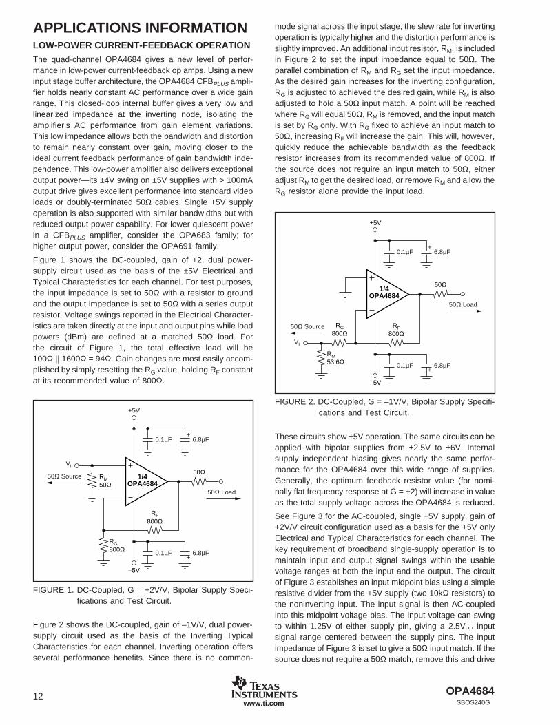
Figure 1 shows the DC-coupled, gain of +2, dual power-supply circuit used as the basis of the ±5V Electrical andTypical Characteristics for each channel. For test purposes,the input impedance is set to 50Ω with a resistor to groundand the output impedance is set to 50Ω with a series outputresistor. Voltage swings reported in the Electrical Character-istics are taken directly at the input and output pins while loadpowers (dBm) are defined at a matched 50Ω load. Forthe circuit of Figure 1, the total effective load will be100Ω || 1600Ω = 94Ω. Gain changes are most easily accom-plished by simply resetting the RG value, holding RF constantat its recommended value of 800Ω.
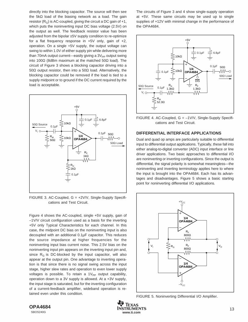
mode signal across the input stage, the slew rate for invertingoperation is typically higher and the distortion performance isslightly improved. An additional input resistor, RM, is includedin Figure 2 to set the input impedance equal to 50Ω. Theparallel combination of RM and RG set the input impedance.As the desired gain increases for the inverting configuration,RG is adjusted to achieved the desired gain, while RM is alsoadjusted to hold a 50Ω input match. A point will be reachedwhere RG will equal 50Ω, RM is removed, and the input matchis set by RG only. With RG fixed to achieve an input match to50Ω, increasing RF will increase the gain. This will, however,quickly reduce the achievable bandwidth as the feedbackresistor increases from its recommended value of 800Ω. Ifthe source does not require an input match to 50Ω, eitheradjust RM to get the desired load, or remove RM and allow theRG resistor alone provide the input load.
RF800Ω
1/4OPA4684
+5V
–5V
50ΩRM50Ω
RG800Ω
50Ω Source
50Ω Load
VI
0.1µF 6.8µF
0.1µF 6.8µF
+
+
FIGURE 1. DC-Coupled, G = +2V/V, Bipolar Supply Speci-fications and Test Circuit.
Figure 2 shows the DC-coupled, gain of –1V/V, dual power-supply circuit used as the basis of the Inverting TypicalCharacteristics for each channel. Inverting operation offersseveral performance benefits. Since there is no common-
RF800Ω
1/4OPA4684
+5V
–5V
50Ω
RM53.6Ω
RG800Ω
50Ω Load
50Ω Source
0.1µF 6.8µF
0.1µF 6.8µF
+
+
VI
FIGURE 2. DC-Coupled, G = –1V/V, Bipolar Supply Specifi-cations and Test Circuit.
These circuits show ±5V operation. The same circuits can beapplied with bipolar supplies from ±2.5V to ±6V. Internalsupply independent biasing gives nearly the same perfor-mance for the OPA4684 over this wide range of supplies.Generally, the optimum feedback resistor value (for nomi-nally flat frequency response at G = +2) will increase in valueas the total supply voltage across the OPA4684 is reduced.
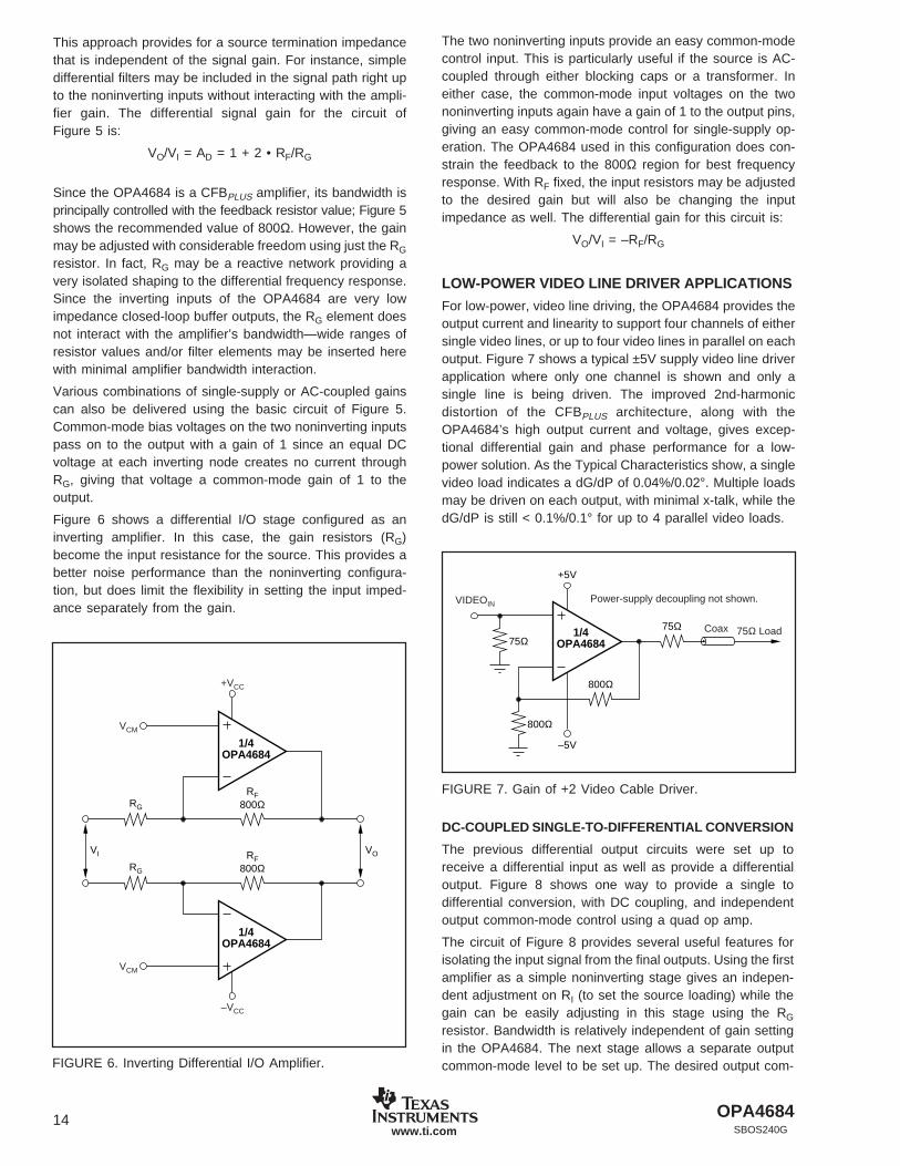
See Figure 3 for the AC-coupled, single +5V supply, gain of+2V/V circuit configuration used as a basis for the +5V onlyElectrical and Typical Characteristics for each channel. Thekey requirement of broadband single-supply operation is tomaintain input and output signal swings within the usablevoltage ranges at both the input and the output. The circuitof Figure 3 establishes an input midpoint bias using a simpleresistive divider from the +5V supply (two 10kΩ resistors) tothe noninverting input. The input signal is then AC-coupledinto this midpoint voltage bias. The input voltage can swingto within 1.25V of either supply pin, giving a 2.5VPP inputsignal range centered between the supply pins. The inputimpedance of Figure 3 is set to give a 50Ω input match. If thesource does not require a 50Ω match, remove this and drive
OPA4684 13SBOS240G www.ti.com
directly into the blocking capacitor. The source will then seethe 5kΩ load of the biasing network as a load. The gainresistor (RG) is AC-coupled, giving the circuit a DC gain of +1,which puts the noninverting input DC bias voltage (2.5V) onthe output as well. The feedback resistor value has beenadjusted from the bipolar ±5V supply condition to re-optimizefor a flat frequency response in +5V only, gain of +2,operation. On a single +5V supply, the output voltage canswing to within 1.0V of either supply pin while delivering morethan 70mA output current—easily giving a 3VPP output swinginto 100Ω (8dBm maximum at the matched 50Ω load). Thecircuit of Figure 3 shows a blocking capacitor driving into a50Ω output resistor, then into a 50Ω load. Alternatively, theblocking capacitor could be removed if the load is tied to asupply midpoint or to ground if the DC current required by theload is acceptable.
Figure 4 shows the AC-coupled, single +5V supply, gain of–1V/V circuit configuration used as a basis for the inverting+5V only Typical Characteristics for each channel. In thiscase, the midpoint DC bias on the noninverting input is alsodecoupled with an additional 0.1µF capacitor. This reducesthe source impedance at higher frequencies for thenoninverting input bias current noise. This 2.5V bias on thenoninverting input pin appears on the inverting input pin and,since RG is DC-blocked by the input capacitor, will alsoappear at the output pin. One advantage to inverting opera-tion is that since there is no signal swing across the inputstage, higher slew rates and operation to even lower supplyvoltages is possible. To retain a 1VPP output capability,operation down to a 3V supply is allowed. At a +3V supply,the input stage is saturated, but for the inverting configurationof a current-feedback amplifier, wideband operation is re-tained even under this condition.
FIGURE 3. AC-Coupled, G = +2V/V, Single-Supply Specifi-cations and Test Circuit.
RF1kΩ
1/4OPA4684
+5V
50Ω
50Ω Load
50Ω Source
0.1µF 6.8µF+
10kΩ
10kΩRM50Ω
RG1kΩ
0.1µF
0.1µF
0.1µF
VI
RF1.3kΩ
1/4OPA4684
+5V
DIS
50Ω
50Ω Load
50Ω Source
0.1µF
0.1µF
6.8µF+
RG1.3kΩ
10kΩ
10kΩ
0.1µF
VI
0.1µF
RM52.3Ω
FIGURE 4. AC-Coupled, G = –1V/V, Single-Supply Specifi-cations and Test Circuit.
The circuits of Figure 3 and 4 show single-supply operationat +5V. These same circuits may be used up to singlesupplies of +12V with minimal change in the performance ofthe OPA4684.
FIGURE 5. Noninverting Differential I/O Amplifier.
RF800Ω
RF800Ω
1/4OPA4684
+VCC
–VCC
RG VO
1/4OPA4684
VI
DIFFERENTIAL INTERFACE APPLICATIONS
Dual and quad op amps are particularly suitable to differentialinput to differential output applications. Typically, these fall intoeither analog-to-digital converter (ADC) input interface or linedriver applications. Two basic approaches to differential I/Oare noninverting or inverting configurations. Since the output isdifferential, the signal polarity is somewhat meaningless—thenoninverting and inverting terminology applies here to wherethe input is brought into the OPA4684. Each has its advan-tages and disadvantages. Figure 5 shows a basic startingpoint for noninverting differential I/O applications.
OPA468414SBOS240Gwww.ti.com
This approach provides for a source termination impedancethat is independent of the signal gain. For instance, simpledifferential filters may be included in the signal path right upto the noninverting inputs without interacting with the ampli-fier gain. The differential signal gain for the circuit ofFigure 5 is:
VO/VI = AD = 1 + 2 • RF/RG
Since the OPA4684 is a CFBPLUS amplifier, its bandwidth isprincipally controlled with the feedback resistor value; Figure 5shows the recommended value of 800Ω. However, the gainmay be adjusted with considerable freedom using just the RG
resistor. In fact, RG may be a reactive network providing avery isolated shaping to the differential frequency response.Since the inverting inputs of the OPA4684 are very lowimpedance closed-loop buffer outputs, the RG element doesnot interact with the amplifier’s bandwidth—wide ranges ofresistor values and/or filter elements may be inserted herewith minimal amplifier bandwidth interaction.
Various combinations of single-supply or AC-coupled gainscan also be delivered using the basic circuit of Figure 5.Common-mode bias voltages on the two noninverting inputspass on to the output with a gain of 1 since an equal DCvoltage at each inverting node creates no current throughRG, giving that voltage a common-mode gain of 1 to theoutput.
Figure 6 shows a differential I/O stage configured as aninverting amplifier. In this case, the gain resistors (RG)become the input resistance for the source. This provides abetter noise performance than the noninverting configura-tion, but does limit the flexibility in setting the input imped-ance separately from the gain.
The two noninverting inputs provide an easy common-modecontrol input. This is particularly useful if the source is AC-coupled through either blocking caps or a transformer. Ineither case, the common-mode input voltages on the twononinverting inputs again have a gain of 1 to the output pins,giving an easy common-mode control for single-supply op-eration. The OPA4684 used in this configuration does con-strain the feedback to the 800Ω region for best frequencyresponse. With RF fixed, the input resistors may be adjustedto the desired gain but will also be changing the inputimpedance as well. The differential gain for this circuit is:
VO/VI = –RF/RG
LOW-POWER VIDEO LINE DRIVER APPLICATIONS
For low-power, video line driving, the OPA4684 provides theoutput current and linearity to support four channels of eithersingle video lines, or up to four video lines in parallel on eachoutput. Figure 7 shows a typical ±5V supply video line driverapplication where only one channel is shown and only asingle line is being driven. The improved 2nd-harmonicdistortion of the CFBPLUS architecture, along with theOPA4684’s high output current and voltage, gives excep-tional differential gain and phase performance for a low-power solution. As the Typical Characteristics show, a singlevideo load indicates a dG/dP of 0.04%/0.02°. Multiple loadsmay be driven on each output, with minimal x-talk, while thedG/dP is still < 0.1%/0.1° for up to 4 parallel video loads.
RF800Ω
RF800Ω
RG
RG
1/4OPA4684
+VCC
–VCC
VCM
VCM
VO
1/4OPA4684
VI
FIGURE 6. Inverting Differential I/O Amplifier.
800Ω
1/4OPA4684
+5V
–5V
75Ω75Ω
800Ω
75Ω Load
Power-supply decoupling not shown.
Coax
VIDEOIN
DC-COUPLED SINGLE-TO-DIFFERENTIAL CONVERSION
The previous differential output circuits were set up toreceive a differential input as well as provide a differentialoutput. Figure 8 shows one way to provide a single todifferential conversion, with DC coupling, and independentoutput common-mode control using a quad op amp.
The circuit of Figure 8 provides several useful features forisolating the input signal from the final outputs. Using the firstamplifier as a simple noninverting stage gives an indepen-dent adjustment on RI (to set the source loading) while thegain can be easily adjusting in this stage using the RG
resistor. Bandwidth is relatively independent of gain settingin the OPA4684. The next stage allows a separate outputcommon-mode level to be set up. The desired output com-
FIGURE 7. Gain of +2 Video Cable Driver.

OPA4684 15SBOS240G www.ti.com
mon-mode voltage, VCM, is cut in half and applied to thenoninverting input of the 2nd stage. The signal path in thisstage sees a gain of –1 while this (1/2 • VCM) voltage sees again of +2. The output of this 2nd stage is then the originalcommon-mode voltage plus the inverted signal from theoutput of the first stage. The 2nd stage output appearsdirectly at the output of the noninverting final stage. Theinverting node of the inverting output stage is also biased tothe common-mode voltage, equal to the common-modevoltage appearing at the output of the 2nd stage, creating nocurrent flow and placing the desired VCM at the output of thisstage as well.
LOW-POWER, DIFFERENTIAL I/O, 4th-ORDER ACTIVE FILTER
The OPA4684 can give a very capable gain block for low-power active filters. The quad design lends itself very well to
800Ω
800Ω
800Ω
1/4OPA4684
+5V
–5V
VCM
VCM
1/4OPA4684
1/4OPA4684
50Ω800Ω800Ω800Ω
1/4OPA4684
+VI (1 + )800Ω
RG
–VI (1 + )800Ω
RG
1kΩ
1kΩ0.1µFRI
RG
VCM
2VI
FIGURE 8. High Gain, DC-Coupled, Single to Differential Conversion.
differential active filters. Where the filter topology is lookingfor a simple gain function to implement the filter, thenoninverting configuration is preferred to isolate the filterelements from the gain elements in the design. Figure 9shows an example of a very low-power, 10MHz, 4th-orderButterworth, low-pass Sallen-Key filter. Often, these filtersare designed at an amplifier gain of 1 to minimize amplifierbandwidth interaction with the desired filter shape. Since theOPA4684 shows minimal bandwidth change with gain, thisfeature would not be a constraint in this design. The exampleof Figure 9 designs the filter for a differential gain of 4 in eachdifferential stage. This DC-coupled design gives a signal gainof 16V/V in the passband with a f–3dB at 10MHz. The designplaces the higher Q stage first to allow the lower Q 2nd stageto roll off the peaked noise of the first stage. The resistorvalues have been adjusted slightly to account for the ampli-fier group delay.
FIGURE 9. Low-Power, Differential I/O, 4th-Order Butterworth Active Filter.
1/4OPA4684
+5V
–5V
1/4OPA4684
392Ω49.9Ω
100pF
392Ω49.9Ω
100pF
800Ω
800Ω534Ω VOVI
1/4OPA4684
1/4OPA4684
249Ω66.5Ω
100pF
100pF
100pF
GD = 4, WO = 2π 10MHz, Q = 0.54GD = 4, WO = 2π 10MHz, Q = 1.31
249Ω66.5Ω
100pF
800Ω
800Ω534Ω
VO/VI = 16V/V
f–3dB = 10MHz
PD = 68mW
100pF
100pF

OPA468416SBOS240Gwww.ti.com
While this circuit is bipolar, using ±5V supplies, it can easilybe adapted to single-supply operation. This is typically doneby providing a supply midpoint reference at the noninvertinginputs then adding DC-blocking caps at each input and inseries with the amplifier gain resistor, RG. This will add tworeal zeroes in the response, transforming this circuit into abandpass. Figure 10 shows the frequency response for thefilter of Figure 9.
LOW-POWER DSL TRANSCEIVER INTERFACE
With four amplifiers available, the quad OPA4684 can meetthe needs for both differential driver and receiver in a low-power xDSL line interface design. Figure 11 shows a simpli-fied design example. Two amplifiers are used as a noninvertingdifferential driver while the other two implement the driverecho cancellation and receiver amplifier function. This ex-ample shows a single +12V design where the drive side istaking a 2VPP maximum input from the transmit filterand providing a differential gain of 7, giving a maximum14VPP differential output swing. This is coupled through 50Ωmatching resistors and a 1:1 transformer to give a maximum7VPP on a 100Ω line. This 7VPP corresponds to a 10dBm linepower with a 3.5 crest factor.
The differential receiver is configured as an inverting sum-ming stage where the outputs of the driver are cancelled priorto appearing at the output of the receive amplifiers. This isdone by summing the output voltages for the drive amplifiers
and their attenuated and inverted levels (at the transformerinput) into the inverting inputs of each receiver amplifier. Theresistor values are set in Figure 11 to give perfect drive signalcancellation if the drive signal is attenuated by 1/2, goingfrom the drive amplifier outputs to the transformer input. Thesignal received through the transformer has a gain of 1through the receive amplifiers. Higher gain could easily beprovided by scaling the resistors summing into the invertinginputs of the receiver amplifiers down while keeping thesame ratio between them.
FIGURE 10. Low-Power, Differential 4th-Order, 10MHz ButterworthResponse.
Frequency (MHz)
Diff
eren
tial G
ain
(dB
)
1 10 100
27
24
21
18
15
12
9
6
3
0
FIGURE 11. Low-Power, XDSL Transceiver Design.
+12V
1/4OPA4684
AFE
1/4OPA4684
900Ω
900Ω300Ω
10kΩ
TransmitFilter
10kΩ
50Ω1:1
100ΩLine
10dBm3.5 Crest Factor
50Ω
2VPP
+6V
ReceiverFilter
1/4OPA4684
1/4OPA4684
800Ω
800Ω
14VPP
VCM
VCM
1.6kΩ 1.6kΩ 800Ω 800Ω
VCM

OPA4684 17SBOS240G www.ti.com
DUAL-CHANNEL, DIFFERENTIAL ADC DRIVER
Where a low-power, single-supply, interface to a differentialinput +5V ADC is required, the circuit of Figure 12 canprovide a high dynamic range, medium gain interface fordual high-performance ADCs. The circuit of Figure 12 usestwo amplifiers in the differential inverting configuration. Thecommon-mode voltage is set on the noninverting inputs tothe supply midscale. In this example, the input signal iscoupled in through a 1:2 transformer. This provides bothsignal gain, single to differential conversion, and a reductionin noise figure. To show a 50Ω input impedance at the inputto the transformer, two 200Ω resistors are required on thetransformer secondary. These two resistors are also theamplifier gain elements. Since the same DC voltage appearson both inverting nodes in the circuit of Figure 12, no DCcurrent will flow through the transformer, giving a DC gain of1 to the output for this common-mode voltage, VCM.
The circuit of Figure 12 is particularly suitable for a moderateresolution dual ADC used as I/Q samplers. The optional500Ω resistors to ground on each amplifier output can beadded to improve the 2nd- and 3rd-harmonic distortion by> 15dB if higher dynamic range is required. Figure 13 showsthe harmonic distortion for the circuit of Figure 12 with andwithout these pull-down resistors. The 5mA added outputstage current significantly improves linearity if that is re-quired. The measured 2nd-harmonic distortion is consis-tently lower than the 3rd-harmonics for this balanced differ-ential design. It is particularly helpful for this low-powerdesign if there are no grounds in the signal path after the low-level signal at the transformer input. The two pull-downresistors do show a signal path ground and should beconnected at the same physical point to ground, in order toeliminate imbalanced ground return currents from degrading2nd-harmonic distortion.
DESIGN-IN TOOLSDEMONSTRATION FIXTURES
Two printed circuit boards (PCBs) are available to assist inthe initial evaluation of circuit performance using the OPA4684in its two package options. Both of these are offered free ofcharge as unpopulated PCBs, delivered with a user's guide.The summary information for these fixtures is shown inTable I.
+5V
1/4OPA4684
1/4OPA4684
800Ω
800Ω
RS
RS
14.7dBNoise Figure
Gain = 8V/V18.1dB
200Ω
200Ω
10kΩ
10kΩ0.1µF
VCM
CL
500Ω
500Ω
VCM
Dual ADC
1 of 2Channels
1:2
50ΩSource
FIGURE 12. Single-Supply Differential ADC Driver (1 of 2 Channels).
ORDERING LITERATUREPRODUCT PACKAGE NUMBER NUMBER
OPA4684ID SO-14 DEM-OPA-SO-4A SBOU016OPA4684IPW TSSOP-14 DEM-OPA-TSSOP-4A SBOU017
TABLE I. Demonstration Fixtures by Package.
FIGURE 13. Harmonic Distortion vs Frequency.
Frequency (MHz)
Har
mon
ic D
isto
rtio
n (d
Bc)
1 10 20
–50
–60
–70
–80
–90
2nd-Harmonic
No Pull-Down
3rd-Harmonic
3rd-Harmonic
2nd-Harmonic
2VPP Output
5mA/Ch Pull-Down
The demonstration fixtures can be requested at the TexasInstruments web site (www.ti.com) through the OPA4684product folder.

OPA468418SBOS240Gwww.ti.com
MACROMODELS
Computer simulation of circuit performance using SPICE isoften useful in predicting the performance of analog circuitsand systems. This is particularly true for Video and RFamplifier circuits where parasitic capacitance and inductancecan have a major effect on circuit performance. Check the TIweb site (www.ti.com) for SPICE macromodels within theOPA4684 product folder. These models do a good job ofpredicting small-signal AC and transient performance undera wide variety of operating conditions. They do not do as wellin predicting distortion or dG/dP characteristics. These mod-els do not attempt to distinguish between the package typesin their small-signal AC performance.
OPERATING SUGGESTIONSSETTING RESISTOR VALUES TO OPTIMIZE BANDWIDTH
Any current-feedback op amp like the OPA4684 can holdhigh bandwidth over signal-gain settings with the properadjustment of the external resistor values. A low-power partlike the OPA4684 typically shows a larger change in band-width due to the significant contribution of the inverting inputimpedance to loop-gain changes as the signal gain is changed.Figure 14 shows a simplified analysis circuit for any current-feedback amplifier.
approaching 1.00; this shows up in a slightly higher CMRRthan previous current-feedback op amps.
RI, the buffer output impedance, is a critical portion of thebandwidth control equation. The OPA4684 reduces thiselement to approximately 4.0Ω using the local loop gain ofthe input buffer stage. This significant reduction in outputimpedance, on very low power, contributes powerfully toextending the bandwidth at higher gains.
A current-feedback op amp senses an error current in theinverting node (as opposed to a differential input error volt-age for a voltage-feedback op amp) and passes this on to theoutput through an internal frequency-dependenttransimpedance gain. The Typical Characteristics show thisopen-loop transimpedance response. This is analogous tothe open-loop voltage gain curve for a voltage-feedback opamp. Developing the transfer function for the circuit of Figure 14gives Equation 1:
(1)
VV
RR
R RRR
Z
NGR R NG
Z
NGRR
O
I
F
G
F IF
G
S
F I
S
F
G
=+
++ +
=+ +
= +
αα
1
1
1 1
1
( )
( )
This is written in a loop-gain analysis format where the errorsarising from a non-infinite open-loop gain are shown in thedenominator. If Z(S) were infinite over all frequencies, thedenominator of Equation 1 would reduce to 1 and the idealdesired signal gain shown in the numerator would be achieved.The fraction in the denominator of Equation 1 determines thefrequency response. Equation 2 shows this as the loop-gainequation.
Z
R R NGLoop GainS
F I
( )
+=
If 20 • log(RF + NG • RI) were drawn on top of the open-looptransimpedance plot, the difference between the two wouldbe the loop gain at a given frequency. Eventually, Z(S) rolls offto equal the denominator of Equation 2 at which point theloop gain has reduced to 1 (and the curves have intersected).This point of equality is where the amplifier’s closed-loopfrequency response given by Equation 1 will start to roll off,and is exactly analogous to the frequency at which the noisegain equals the open-loop voltage gain for a voltage feed-back op amp. The difference here is that the total impedancein the denominator of Equation 2 may be controlled some-what separately from the desired signal gain (or NG).
The OPA4684 is internally compensated to give a maximallyflat frequency response for RF = 800Ω at NG = 2 on ±5Vsupplies. That optimum value goes to 1.0kΩ on a single +5Vsupply. Normally, with a current-feedback amplifier, it is
RF
VO
RG
RIZ(S) iERR
iERR
α
VI
FIGURE 14. Current-Feedback Transfer Function AnalysisCircuit.
The key elements of this current-feedback op amp modelare:
α ⇒ Buffer gain from the noninverting input to the inverting inputRI ⇒ Buffer output impedance
iERR ⇒ Feedback error current signal
Z(S) ⇒ Frequency-dependent open-loop transimpedance gainfrom iERR to VO
The buffer gain is typically very close to 1.00 and is normallyneglected from signal gain considerations. It will, however,set the CMRR for a single op amp differentialamplifier configuration. For the buffer gain α < 1.0, theCMRR = –20 • log(1 – α). The closed-loop input stage bufferused in the OPA4684 gives a buffer gain more closely
(2)

OPA4684 19SBOS240G www.ti.com
possible to adjust the feedback resistor to hold this band-width up as the gain is increased. The CFBPLUS architecturehas reduced the contribution of the inverting input impedanceto provide exceptional bandwidth to higher gains withoutadjusting the feedback resistor value. The Typical Character-istics show the small-signal bandwidth over gain with a fixedfeedback resistor.
Putting a closed-loop buffer between the noninverting andinverting inputs does bring some added considerations. Sincethe voltage at the inverting output node is now the output ofa locally closed-loop buffer, parasitic external capacitance onthis node can cause frequency response peaking for thetransfer function from the noninverting input voltage to theinverting node voltage. While it is always important to keepthe inverting node capacitance low for any current-feedbackop amp, it is critically important for the OPA4684. Externallayout capacitance in excess of 2pF will start to peak thefrequency response. This peaking can be easily reduced bythen increasing the feedback resistor value—but it is prefer-able, from a noise and dynamic range standpoint, to keepthat capacitance low, allowing a close to nominal 800Ωfeedback resistor for flat frequency response. Very highparasitic capacitance values on the inverting node (> 5pF)can possibly cause input stage oscillation that cannot befiltered by a feedback element adjustment.
At very high gains, 2nd-order effects in the inverting outputimpedance cause the overall response to peak up. If desired,it is possible to retain a flat frequency response at highergains by adjusting the feedback resistor to higher values asthe gain is increased. Since the exact value of feedback thatwill give a flat frequency response depends strongly ininverting and output node parasitic capacitance values, it isbest to experiment in the specific board with increasingvalues until the desired flatness (or pulse response shape) isobtained. In general, increasing RF (and then adjusting RG tothe desired gain) will move towards flattening the response,while decreasing it will extend the bandwidth at the cost ofsome peaking.
OUTPUT CURRENT AND VOLTAGE
The OPA4684 provides output voltage and current capabili-ties that can support the needs of driving doubly-terminated50Ω lines. For a 100Ω load at the gain of +2, (see Figure 1),the total load is the parallel combination of the 100Ω load andthe 1.6kΩ total feedback network impedance. This 94Ω loadwill require no more than 40mA output current to supportthe ±3.8V minimum output voltage swing specified for100Ω loads. This is well under the specified minimum+110mA/–90mA output current specifications over the fulltemperature range.
The specifications described above, though familiar in theindustry, consider voltage and current limits separately. Inmany applications, it is the voltage • current, or V-I product,which is more relevant to circuit operation. Refer to theOutput Voltage and Current Limitations curve in the TypicalCharacteristics. The X- and Y-axes of this graph show thezero-voltage output current limit and the zero-current outputvoltage limit, respectively. The four quadrants give a more
detailed view of the OPA4684’s output drive capabilities.Superimposing resistor load lines onto the plot shows theavailable output voltage and current for specific loads.
The minimum specified output voltage and current overtemperature are set by worst-case simulations at the coldtemperature extreme. Only at cold startup will the outputcurrent and voltage decrease to the numbers shown in theElectrical Characteristic tables. As the output transistorsdeliver power, their junction temperatures will increase, de-creasing their VBEs (increasing the available output voltageswing) and increasing their current gains (increasing theavailable output current). In steady-state operation, the avail-able output voltage and current will always be greater thanthat shown in the over temperature specifications since theoutput stage junction temperatures will be higher than theminimum specified operating ambient.
To maintain maximum output stage linearity, no output short-circuit protection is provided. This will not normally be aproblem since most applications include a series-matchingresistor at the output that will limit the internal power dissipa-tion if the output side of this resistor is shorted to ground.However, shorting the output pin directly to a power-supplypin will, in most cases, destroy the amplifier. If additionalshort-circuit protection is required, consider a small-seriesresistor in the power-supply leads. This will, under heavyoutput loads, reduce the available output voltage swing. A 5Ωseries resistor in each power-supply lead will limit the internalpower dissipation to less than 1W for an output short-circuitwhile decreasing the available output voltage swing only0.25V for up to 50mA desired load currents. This slight dropin available swing is more if multiple channels are drivingheavy loads simultaneously. Always place the 0.1µF power-supply decoupling capacitors after these supply current lim-iting resistors, directly on the supply pins.
DRIVING CAPACITIVE LOADS
One of the most demanding, and yet very common, loadconditions for an op amp is capacitive loading. Often, thecapacitive load is the input of an ADC—including additionalexternal capacitance which may be recommended to im-prove ADC linearity. A high-speed, high open-loop gainamplifier like the OPA4684 can be very susceptible to de-creased stability and closed-loop response peaking when acapacitive load is placed directly on the output pin. When theamplifier’s open-loop output resistance is considered, thiscapacitive load introduces an additional pole in the signalpath that can decrease the phase margin. Several externalsolutions to this problem have been suggested. When theprimary considerations are frequency response flatness, pulseresponse fidelity, and/or distortion, the simplest and mosteffective solution is to isolate the capacitive load from thefeedback loop by inserting a series isolation resistor betweenthe amplifier output and the capacitive load. This does noteliminate the pole from the loop response, but rather shifts itand adds a zero at a higher frequency. The additional zeroacts to cancel the phase lag from the capacitive load pole,thus increasing the phase margin and improving stability.

OPA468420SBOS240Gwww.ti.com
The Typical Characteristics show the recommended RS vsCLOAD and the resulting frequency response at the load. The1kΩ resistor shown in parallel with the load capacitor is ameasurement path and may be omitted. Parasitic capacitiveloads greater than 5pF can begin to degrade the perfor-mance of the OPA4684. Long PCB traces, unmatched cables,and connections to multiple devices can easily cause thisvalue to be exceeded. Always consider this effect carefully,and add the recommended series resistor as close as pos-sible to the OPA4684 output pin (see the Board LayoutGuidelines section).
DISTORTION PERFORMANCE
The OPA4684 provides very low distortion in a low-powerpart. The CFBPLUS architecture also gives two significantareas of distortion improvement. First, in operating regionswhere the 2nd-harmonic distortion due to output stagenonlinearities is very low (frequencies < 1MHz, low outputswings into light loads), the linearization at the inverting nodeprovided by the CFBPLUS design gives 2nd-harmonic distor-tions that extend into the –90dBc region. Previous current-feedback amplifiers have been limited to approximately–85dBc due to the nonlinearities at the inverting input. Thesecond area of distortion improvement comes in a distortionperformance that is largely gain independent. To the extentthat the distortion at a particular output power is output stagedependent, 3rd-harmonics particularly, and to a lesser extent2nd-harmonic distortion, is constant as the gain is increased.This is due to the constant loop gain versus signal gainprovided by the CFBPLUS design. As shown in the TypicalCharacteristic curves, while the 3rd-harmonic is constantwith gain, the 2nd-harmonic degrades at higher gains. Thisis largely due to board parasitic issues. Slightly imbalancedload return currents will couple into the gain resistor to causea portion of the 2nd-harmonic distortion. At high gains, thisimbalance has more gain to the output giving reduced 2nd-harmonic distortion. Differential stages using two of thechannels together can reduce this 2nd-harmonic issue enor-mously getting back to an essentially gain independentdistortion.
Relative to alternative amplifiers with < 2mA/ch supply cur-rent, the OPA4684 holds much lower distortion at higherfrequencies (> 5MHz) and to higher gains. Generally, untilthe fundamental signal reaches very high frequency or powerlevels, the 2nd-harmonic will dominate the distortion with alower 3rd-harmonic component. Focusing then on the 2nd-harmonic, increasing the load impedance improves distortiondirectly. Remember that the total load includes the feedbacknetwork—in the noninverting configuration (see Figure 1) thisis the sum of RF + RG, while in the inverting configuration itis just RF. Also, providing an additional supply decouplingcapacitor (0.1µF) between the supply pins (for bipolar opera-tion) improves the 2nd-order distortion slightly (3dB to 6dB).
In most op amps, increasing the output voltage swing in-creases harmonic distortion directly. A low-power part likethe OPA4684 includes quiescent boost circuits to provide thelarge-signal bandwidth in the Electrical Characteristics. Theseact to increase the bias in a very linear fashion only when
high slew rate or output power are required. This also acts toactually reduce the distortion slightly at higher output powerlevels. The Typical Characteristic curves show the 2nd-harmonic holding constant from 500mVPP to 5VPP outputswhile the 3rd-harmonics actually decrease with increasingoutput power.
The OPA4684 has an extremely low 3rd-order harmonicdistortion, particularly for light loads and at lower frequen-cies. This also gives low 2-tone, 3rd-order intermodulationdistortion as shown in the Typical Characteristic curves.Since the OPA4684 includes internal power boost circuits toretain good full-power performance at high frequencies andoutputs, it does not show a classical 2-tone, 3rd-orderintermodulation intercept characteristic. Instead, it holds rela-tively low and constant 3rd-order intermodulation spuriouslevels over power. The Typical Characteristic curves showthis spurious level as a dBc below the carrier at fixed centerfrequencies swept over single-tone power at a matched 50Ωload. These spurious levels drop significantly (> 12dB) forloads lighter than the 100Ω used in the 2-Tone, 3rd-OrderIntermodulation Distortion curve. Converter inputs, for in-stance, will see < –82dBc 3rd-order spurious to 10MHz forfull-scale inputs. For even lower 3rd-order intermodulationdistortion to much higher frequencies, consider the OPA2691dual or OPA691 and OPA695 single-channel current-feed-back amplifiers.
NOISE PERFORMANCEWideband current-feedback op amps generally have a higheroutput noise than comparable voltage-feedback op amps.The OPA4684 offers an excellent balance between voltageand current noise terms to achieve low output noise in a low-power amplifier. The inverting current noise (17pA/√Hz) iscomparable to most other current-feedback op amps whilethe input voltage noise (3.7nV/√Hz) is lower than any unity-gain stable, comparable slew rate, voltage-feedback op amp.This low input voltage noise was achieved at the price ofhigher noninverting input current noise (9.4pA/√Hz). As longas the AC source impedance looking out of the noninvertingnode is less than 200Ω, this current noise will not contributesignificantly to the total output noise. The op amp inputvoltage noise and the two input current noise terms combineto give low output noise under a wide variety of operatingconditions. Figure 15 shows the op amp noise analysismodel with all the noise terms included. In this model, allnoise terms are taken to be noise voltage or current densityterms in either nV/√Hz or pA/√Hz.
FIGURE 15. Op Amp Noise Analysis Model.
4kTRG
RG
RF
RS
1/4OPA4684
IBI
EO
IBN
4kT = 1.6E –20Jat 290°K
ERS
ENI
4kTRS√4kTRF√

OPA4684 21SBOS240G www.ti.com
The total output spot noise voltage can be computed as thesquare root of the sum of all squared output noise voltagecontributors. Equation 3 shows the general form for theoutput noise voltage using the terms presented in Figure 12.
(3)
E E I R kTR G I R kTR GO NI BN S S N BI F F N= + ( ) +
+ ( ) +2 2 2 2
4 4
Dividing this expression by the noise gain (GN = (1+RF/RG))will give the equivalent input referred spot noise voltage atthe noninverting input, as shown in Equation 4.
(4)
E E I R kTRI RG
kTRGN NI BN S S
BI F
N
F
N= + ( ) + +
+2 22
44
Evaluating these two equations for the OPA4684 circuit andcomponent values presented in Figure 1 will give a totaloutput spot noise voltage of 16.3nV/√Hz and a total equiva-lent input spot noise voltage of 8.1nV/√Hz. This total inputreferred spot noise voltage is higher than the 3.7nV/√Hzspecification for the op amp voltage noise alone. This re-flects the noise added to the output by the inverting currentnoise times the feedback resistor. As the gain is increased,this fixed output noise power term contributes less to thetotal output noise and the total input referred voltage noisegiven by Equation 3 will approach just the 3.7nV/√Hz of theop amp itself. For example, going to a gain of +20 in thecircuit of Figure 1, adjusting only the gain resistor to 42.1Ω,will give a total input referred noise of 3.9nV/√Hz. A morecomplete description of op amp noise analysis can be foundin the Texas Instruments application note, AB-103, NoiseAnalysis for High Speed Op Amps (SBOA066), available fordownload at www.ti.com.
DC ACCURACY AND OFFSET CONTROL
A current-feedback op amp like the OPA4684 providesexceptional bandwidth in high gains, giving fast pulse settlingbut only moderate DC accuracy. The Electrical Characteris-tics show an input offset voltage comparable to high slewrate voltage-feedback amplifiers. However, the two inputbias currents are somewhat higher and are unmatched.Whereas bias current cancellation techniques are very effec-tive with most voltage-feedback op amps, they do not gen-erally reduce the output DC offset for wideband current-feedback op amps. Since the two input bias currents areunrelated in both magnitude and polarity, matching thesource impedance looking out of each input to reduce theirerror contribution to the output is ineffective. Evaluating the
configuration of Figure 1, using worst-case +25°C input offsetvoltage and the two input bias currents, gives a worst-caseoutput offset range equal to:
±(NG • VOS(MAX)) + (IBN • RS/2 • NG) ± (IBI • RF)
where NG = noninverting signal gain
= ±(2 • 4.0mV) ± (13µA • 25Ω • 2) ± (800Ω • 17µA)
= ±8mV + 0.65mV ± 13.6mV
= ±22.3mV
While the last term, the inverting bias current error, isdominant in this low-gain circuit, the input offset voltage willbecome the dominant DC error term as the gain exceeds5V/V. Where improved DC precision is required in a high-speed amplifier, consider the OPA656 single and OPA4820quad voltage-feedback amplifiers.
THERMAL ANALYSIS
The OPA4684 will not require external heatsinking or airflowmost applications. Maximum desired junction temperaturewill set the maximum allowed internal power dissipation asdescribed below. In no case should the maximum junctiontemperature be allowed to exceed 150°C.
Operating junction temperature (TJ) is given by TA + PD • θJA.The total internal power dissipation (PD) is the sum ofquiescent power (PDQ) and additional power dissipated in theoutput stage (PDL) to deliver load power. Quiescent power issimply the specified no-load supply current times the totalsupply voltage across the part. PDL depends on the requiredoutput signal and load; for a grounded resistive load, PDL
would be at a maximum when the output is fixed at a voltageequal to 1/2 either supply voltage (for equal bipolar supplies).Under this condition PDL = VS
2/(4 • RL), where RL includesfeedback network loading.
Note that it is the power in the output stage and not into theload that determines internal power dissipation.
As an absolute worst-case example, compute the maximumTJ using an OPA4684IPW (TSSOP-14 package) in the circuitof Figure 1 operating at the maximum specified ambienttemperature of +85°C with all channels driving a grounded100Ω load to 2.5VDC.
PD = 10V • 7.8mA + 4 • (52 /(4 • (100Ω 1.6kΩ))) = 144mWMaximum TJ = +85°C + (0.144W • 110°C/W) = 101°C.
This maximum operating junction temperature is well belowmost system level targets. Most applications will be lowerthan this since an absolute worst-case output stage powerwas assumed in this calculation with all four channels run-ning maximum output power simultaneously.

OPA468422SBOS240Gwww.ti.com
BOARD LAYOUT GUIDELINES
Achieving optimum performance with a high-frequency am-plifier like the OPA4684 requires careful attention to boardlayout parasitics and external component types. Recommen-dations that will optimize performance include:
a) Minimize parasitic capacitance to any AC ground forall of the signal I/O pins. Parasitic capacitance on theoutput and inverting input pins can cause instability; onthe noninverting input, it can react with the sourceimpedance to cause unintentional bandlimiting. To re-duce unwanted capacitance, a window around the sig-nal I/O pins should be opened in all of the ground andpower planes around those pins. Otherwise, ground andpower planes should be unbroken elsewhere on theboard.
b) Minimize the distance (< 0.25") from the power-supplypins to high-frequency 0.1µF decoupling capacitors. Atthe device pins, the ground and power-plane layoutshould not be in close proximity to the signal I/O pins.Avoid narrow power and ground traces to minimizeinductance between the pins and the decoupling capaci-tors. The power-supply connections should always bedecoupled with these capacitors. An optional supply de-coupling capacitor (0.01µF) across the two power sup-plies (for bipolar operation) will improve 2nd-harmonicdistortion performance. Larger (2.2µF to 6.8µF)decoupling capacitors, effective at lower frequencies,should also be used on the main supply pins. Thesemay be placed somewhat farther from the device andmay be shared among several devices in the same areaof the PCB.
c) Careful selection and placement of external compo-nents will preserve the high-frequency performanceof the OPA4684. Resistors should be a very low reac-tance type. Surface-mount resistors work best and allowa tighter overall layout. Metal film and carbon composi-tion axially-leaded resistors can also provide good high-frequency performance. Again, keep their leads andPCB trace length as short as possible. Never usewirewound type resistors in a high-frequency applica-tion. Since the output pin and inverting input pin are themost sensitive to parasitic capacitance, always positionthe feedback and series output resistor, if any, as closeas possible to the output pin. The quad amplifier pinoutallows each output and inverting input to be connectedby the feedback element with virtually no trace length.Other network components, such as noninverting inputtermination resistors, should also be placed close to thepackage. The frequency response is primarily deter-mined by the feedback resistor value as describedpreviously. Increasing its value will reduce the peakingat higher gains, while decreasing it will give a morepeaked frequency response at lower gains. The 800Ωfeedback resistor used in the Typical Characteristics ata gain of +2 on ±5V supplies is a good starting point for
design. Note that a 800Ω feedback resistor, rather thana direct short, is required for the unity-gain followerapplication. A current-feedback op amp requires a feed-back resistor even in the unity-gain follower configura-tion to control stability.
d) Connections to other wideband devices on the boardmay be made with short direct traces or through onboardtransmission lines. For short connections, consider thetrace and the input to the next device as a lumpedcapacitive load. Relatively wide traces (50mils to 100mils)should be used, preferably with ground and powerplanes opened up around them. Estimate the total ca-pacitive load and set RS from the plot of recommendedRS vs CLOAD. Low parasitic capacitive loads(< 5pF) may not need an RS since the OPA4684 isnominally compensated to operate with a 2pF parasiticload. If a long trace is required, and the 6dB signal lossintrinsic to a doubly-terminated transmission line is ac-ceptable, implement a matched impedance transmis-sion line using microstrip or stripline techniques (consultan ECL design handbook for microstrip and striplinelayout techniques). A 50Ω environment is normally notnecessary on board, and in fact a higher impedanceenvironment will improve distortion; see the distortionversus load plots. With a characteristic board traceimpedance defined based on board material and tracedimensions, a matching series resistor into the tracefrom the output of the OPA4684 is used, as well as aterminating shunt resistor at the input of the destinationdevice. Remember also that the terminating impedancewill be the parallel combination of the shunt resistor andthe input impedance of the destination device; this totaleffective impedance should be set to match the traceimpedance. The high output voltage and current capabil-ity of the OPA4684 allows multiple destination devices tobe handled as separate transmission lines, each withtheir own series and shunt terminations. If the 6dBattenuation of a doubly-terminated transmission line isunacceptable, a long trace can be series-terminated atthe source end only. Treat the trace as a capacitive loadin this case and set the series resistor value as shownin the plot of RS vs CLOAD. This will not preserve signalintegrity as well as a doubly-terminated line. If the inputimpedance of the destination device is low, there will besome signal attenuation due to the voltage divider formedby the series output into the terminating impedance.
e) Socketing a high-speed part like the OPA4684 is notrecommended. The additional lead length and pin-to-pin capacitance introduced by the socket can create anextremely troublesome parasitic network, which canmake it almost impossible to achieve a smooth, stablefrequency response. Best results are obtained by sol-dering the OPA4684 onto the board.

OPA4684 23SBOS240G www.ti.com
INPUT AND ESD PROTECTION
The OPA4684 is built using a very high-speed complemen-tary bipolar process. The internal junction breakdown volt-ages are relatively low for these very small geometry de-vices. These breakdowns are reflected in the Absolute Maxi-mum Ratings table where an absolute maximum 13V acrossthe supply pins is reported. All device pins have limited ESDprotection using internal diodes to the power supplies, asshown in Figure 16.
These diodes provide moderate protection to input overdrivevoltages above the supplies as well. The protection diodescan typically support 30mA continuous current. Where highercurrents are possible (for example, in systems with ±15Vsupply parts driving into the OPA4684), current limitingseries resistors should be added into the two inputs. Keepthese resistor values as low as possible since high valuesdegrade both noise performance and frequency response.
ExternalPin
+VCC
–VCC
InternalCircuitry
FIGURE 16. Internal ESD Protection.

OPA468424SBOS240Gwww.ti.com
Revision History
DATE REVISION PAGE SECTION DESCRIPTION
Changed Storage Temperature Range from −40°C to +125C to−65°C to +125C.
3, 4 Added minimum supply voltage. Changed min and max quiescent currentvalues from total to per channel.
17 Design-In Tools Demonstration fixture numbers changed.
24 Applications Information Added Revision History table.
NOTE: Page numbers for previous revisions may differ from page numbers in the current version.
6/06 F
7/08 G2 Abs Max Ratings
Electrical Characteristics,Power Supply

PACKAGE OPTION ADDENDUM
www.ti.com 13-Aug-2021
Addendum-Page 1
PACKAGING INFORMATION
Orderable Device Status(1)
Package Type PackageDrawing
Pins PackageQty
Eco Plan(2)
Lead finish/Ball material
(6)
MSL Peak Temp(3)
Op Temp (°C) Device Marking(4/5)
Samples
OPA4684ID ACTIVE SOIC D 14 50 RoHS & Green NIPDAU Level-2-260C-1 YEAR -40 to 85 OPA4684
OPA4684IDG4 ACTIVE SOIC D 14 50 RoHS & Green NIPDAU Level-2-260C-1 YEAR -40 to 85 OPA4684
OPA4684IDR ACTIVE SOIC D 14 2500 RoHS & Green NIPDAU Level-2-260C-1 YEAR -40 to 85 OPA4684
OPA4684IPWT ACTIVE TSSOP PW 14 250 RoHS & Green NIPDAU Level-2-260C-1 YEAR -40 to 85 OPA4684
(1) The marketing status values are defined as follows:ACTIVE: Product device recommended for new designs.LIFEBUY: TI has announced that the device will be discontinued, and a lifetime-buy period is in effect.NRND: Not recommended for new designs. Device is in production to support existing customers, but TI does not recommend using this part in a new design.PREVIEW: Device has been announced but is not in production. Samples may or may not be available.OBSOLETE: TI has discontinued the production of the device.
(2) RoHS: TI defines "RoHS" to mean semiconductor products that are compliant with the current EU RoHS requirements for all 10 RoHS substances, including the requirement that RoHS substancedo not exceed 0.1% by weight in homogeneous materials. Where designed to be soldered at high temperatures, "RoHS" products are suitable for use in specified lead-free processes. TI mayreference these types of products as "Pb-Free".RoHS Exempt: TI defines "RoHS Exempt" to mean products that contain lead but are compliant with EU RoHS pursuant to a specific EU RoHS exemption.Green: TI defines "Green" to mean the content of Chlorine (Cl) and Bromine (Br) based flame retardants meet JS709B low halogen requirements of <=1000ppm threshold. Antimony trioxide basedflame retardants must also meet the <=1000ppm threshold requirement.
(3) MSL, Peak Temp. - The Moisture Sensitivity Level rating according to the JEDEC industry standard classifications, and peak solder temperature.
(4) There may be additional marking, which relates to the logo, the lot trace code information, or the environmental category on the device.
(5) Multiple Device Markings will be inside parentheses. Only one Device Marking contained in parentheses and separated by a "~" will appear on a device. If a line is indented then it is a continuationof the previous line and the two combined represent the entire Device Marking for that device.
(6) Lead finish/Ball material - Orderable Devices may have multiple material finish options. Finish options are separated by a vertical ruled line. Lead finish/Ball material values may wrap to twolines if the finish value exceeds the maximum column width.
Important Information and Disclaimer:The information provided on this page represents TI's knowledge and belief as of the date that it is provided. TI bases its knowledge and belief on informationprovided by third parties, and makes no representation or warranty as to the accuracy of such information. Efforts are underway to better integrate information from third parties. TI has taken and
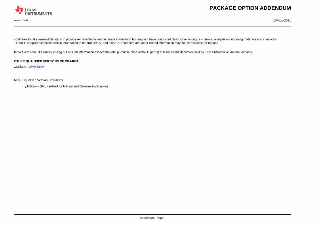
PACKAGE OPTION ADDENDUM
www.ti.com 13-Aug-2021
Addendum-Page 2
continues to take reasonable steps to provide representative and accurate information but may not have conducted destructive testing or chemical analysis on incoming materials and chemicals.TI and TI suppliers consider certain information to be proprietary, and thus CAS numbers and other limited information may not be available for release.
In no event shall TI's liability arising out of such information exceed the total purchase price of the TI part(s) at issue in this document sold by TI to Customer on an annual basis.
OTHER QUALIFIED VERSIONS OF OPA4684 :
• Military : OPA4684M
NOTE: Qualified Version Definitions:
• Military - QML certified for Military and Defense Applications

TAPE AND REEL INFORMATION
*All dimensions are nominal
Device PackageType
PackageDrawing
Pins SPQ ReelDiameter
(mm)
ReelWidth
W1 (mm)
A0(mm)
B0(mm)
K0(mm)
P1(mm)
W(mm)
Pin1Quadrant
OPA4684IDR SOIC D 14 2500 330.0 16.4 6.5 9.0 2.1 8.0 16.0 Q1
OPA4684IPWT TSSOP PW 14 250 180.0 12.4 6.9 5.6 1.6 8.0 12.0 Q1
PACKAGE MATERIALS INFORMATION
www.ti.com 5-Jan-2022
Pack Materials-Page 1
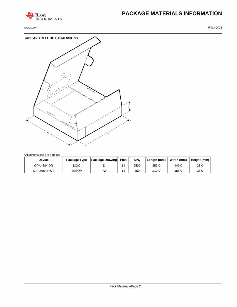
*All dimensions are nominal
Device Package Type Package Drawing Pins SPQ Length (mm) Width (mm) Height (mm)
OPA4684IDR SOIC D 14 2500 853.0 449.0 35.0
OPA4684IPWT TSSOP PW 14 250 210.0 185.0 35.0
PACKAGE MATERIALS INFORMATION
www.ti.com 5-Jan-2022
Pack Materials-Page 2
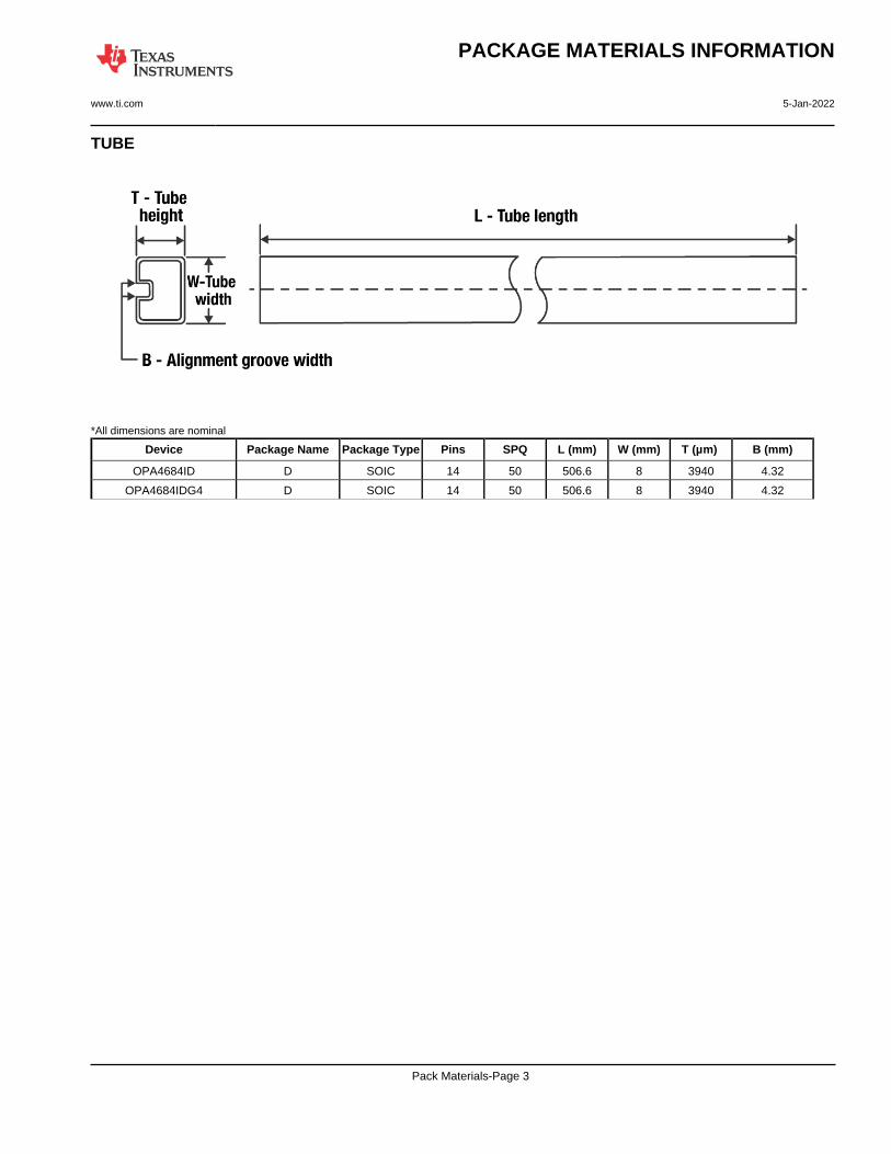
TUBE
*All dimensions are nominal
Device Package Name Package Type Pins SPQ L (mm) W (mm) T (µm) B (mm)
OPA4684ID D SOIC 14 50 506.6 8 3940 4.32
OPA4684IDG4 D SOIC 14 50 506.6 8 3940 4.32
PACKAGE MATERIALS INFORMATION
www.ti.com 5-Jan-2022
Pack Materials-Page 3
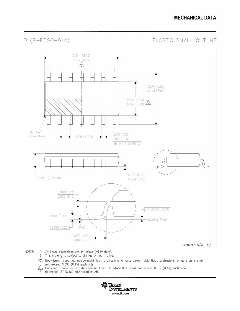
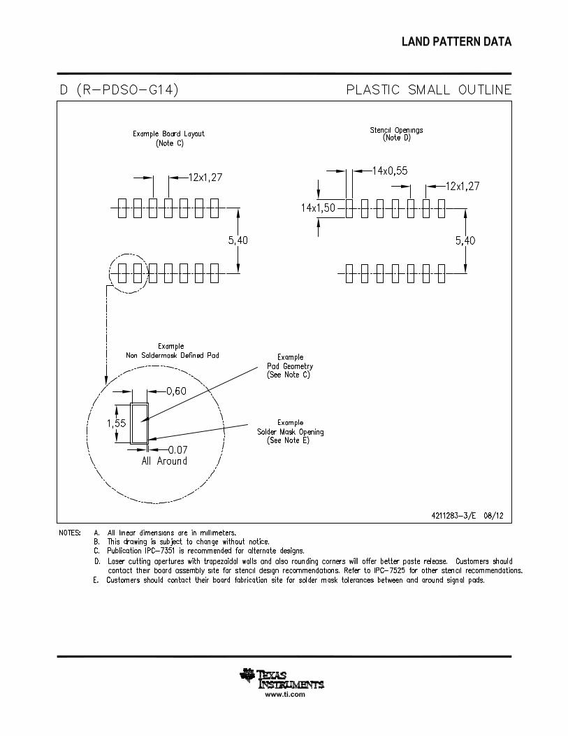


IMPORTANT NOTICE AND DISCLAIMERTI PROVIDES TECHNICAL AND RELIABILITY DATA (INCLUDING DATA SHEETS), DESIGN RESOURCES (INCLUDING REFERENCE DESIGNS), APPLICATION OR OTHER DESIGN ADVICE, WEB TOOLS, SAFETY INFORMATION, AND OTHER RESOURCES “AS IS” AND WITH ALL FAULTS, AND DISCLAIMS ALL WARRANTIES, EXPRESS AND IMPLIED, INCLUDING WITHOUT LIMITATION ANY IMPLIED WARRANTIES OF MERCHANTABILITY, FITNESS FOR A PARTICULAR PURPOSE OR NON-INFRINGEMENT OF THIRD PARTY INTELLECTUAL PROPERTY RIGHTS.These resources are intended for skilled developers designing with TI products. You are solely responsible for (1) selecting the appropriate TI products for your application, (2) designing, validating and testing your application, and (3) ensuring your application meets applicable standards, and any other safety, security, regulatory or other requirements.These resources are subject to change without notice. TI grants you permission to use these resources only for development of an application that uses the TI products described in the resource. Other reproduction and display of these resources is prohibited. No license is granted to any other TI intellectual property right or to any third party intellectual property right. TI disclaims responsibility for, and you will fully indemnify TI and its representatives against, any claims, damages, costs, losses, and liabilities arising out of your use of these resources.TI’s products are provided subject to TI’s Terms of Sale or other applicable terms available either on ti.com or provided in conjunction with such TI products. TI’s provision of these resources does not expand or otherwise alter TI’s applicable warranties or warranty disclaimers for TI products.TI objects to and rejects any additional or different terms you may have proposed. IMPORTANT NOTICE
Mailing Address: Texas Instruments, Post Office Box 655303, Dallas, Texas 75265Copyright © 2022, Texas Instruments Incorporated