


File Number Here ® Spartan-II FPGAs in Set-top Boxes - Sales Tutorial.
1FEATURES
APPLICATIONS
DESCRIPTION/ORDERING INFORMATION
TPS65230, TPS65231
www.ti.com .................................................................................................................................... SLVSA10A–SEPTEMBER 2009–REVISED SEPTEMBER 2009
POWER MANAGEMENT IC FOR DIGITAL SET TOP BOXES• Supply Voltage Supervisor Circuit with Two
Monitor Inputs and Open Drain Output• Wide Input Supply Voltage Range(10.8 V - 22 V) • Parallel I/O or I2C Control with User Selectable
Address• One Adjustable PWM Buck Controller• Advanced Fault Detection and Output Voltage– 10.8-V - 22-V Input Voltage Range
Adjustment Options in I2C Mode– 3.3-V - 6.1-V Output Voltage Range• Pull-Up Current Sources on Buck Enable Pins– 500kHz switching frequency
for Accurate Start-Up Timing Control with– Type III Compensation Preset Default– Programmable Current Limit • Over Current Protection on All Rails
• Two Adjustable Step-Down Converter with • Thermal Shutdown to Protect Device DuringIntegrated Switching FETs: Excessive Power Dissipation– 4.75-V - 5.5-V Input • Thermally Enhanced Package for Efficient– 0.9-V-3.3-V Output Voltage Range Heat Management (48-pin HTSSOP)– 3-A Output Current– 1-MHz Switching Frequency
• Digital Set Top Boxes– Voltage Scaling Option• xDSL & Cable Modems– Type III Compensation• DVD Players• Two 100-mΩ, 0.5-A (TPS65230) 1-A (TPS65231)• Home Gateway and Access Point NetworksUSB Switches with Over Current Protection• Wireless Routersand Open-Drain Fault Pin
• Early Supply Failure Flag (Open Drain Output)is Set when Input Voltage Drops Below 9.3 V
• Early Temperature Warning Flag (Open DrainOutput) is Set if Temperature ApproachesShut-Down Threshold
The TPS652x provides one PWM buck controller, two adjustable, synchronous buck regulators, two independentUSB power switches and a supply voltage supervisor (SVS) to provide main power functions for satellite set topboxes, xDSL and cable modem applications operating off a single 12- to 22-V supply.
The SMPS have integrated switching FETs for optimized power efficiency and reduced external componentcount. Each USB switch provides up to 0.5-A (TPS65230) or 1-A (TPS65231) of current as required bydownstream USB devices. All power blocks have thermal and over current/short circuit protection.
The SVS provides two inputs for monitoring positive supply rails. The active-low open-drain output remains lowfor at least 180 ms after all supply rails rise above their rising edge threshold. Threshold value for VMON1 inputis set for monitoring a 3.3-V rail without the need for additional external components. Threshold for VMON2 inputis set to 0.8 V and requires resistor dividers on the input to monitor any positive voltage in the system. ThenBOR/nHOT open-drain output is pulled low if the input supply drops below 9.3 V or the chip temperatureapproaches the thermal shutdown limit. This allows the system processor to save critical data and shut downgracefully before the supply fails.
1
Please be aware that an important notice concerning availability, standard warranty, and use in critical applications of TexasInstruments semiconductor products and disclaimers thereto appears at the end of this data sheet.
PRODUCTION DATA information is current as of publication date. Copyright © 2009, Texas Instruments IncorporatedProducts conform to specifications per the terms of the TexasInstruments standard warranty. Production processing does notnecessarily include testing of all parameters.
Not Recommended for New Designs

REF
RESET GENERATOR
OSC
UVLO
TRIM
VIN
f ro m e na ble log ic
EN_BCK1
EN_BCK2
EN_BCK3
1 2V DC Sup ply
t o u C or DSP
f ro m e na ble log ic
f ro m e na ble log ic
nRST
PG
ND
PG
ND
AG
ND
DG
ND
VM ON1
BUCK1
BST1
LDRV
FB1
CM P1
VIN
PH2a
PH2b
FB2
CM P2
PH3a
PH3b
FB3
Vou t BUCK3
CM P3
INTERNAL
VO LT AGE RAILS
TSD
Vou t BUC K1
HDRV
1 2V
ENUSB1 /SCL
fro m uC o r DSP
EENUSB2/SDA
VREF1
VIN
B3
b
VM ON2
I2C
INT
to uC or DSP
Fr om 3. 3v s up py
f ro m pos mo nit or Sup ply
VIN
B3
a
VINB and VINBQ pins must be t ied
t og the ron PC board
Op tion al
V3p3
VLSD
I2C_ADD
VIN
B2
b
VIN
B2
a
DIG
ITA
LL
OG
IC
VREF2
fro m uC o r DSP
BST3
BST2
PH1
Vou t BUCK2
PG
ND
BUCK3
VINB3
BUCK2
VINB2
PG
ND
USB1 USBO UT 1
USBF LG1/CTRL
V3p3
To USB p ort
To/f rom u C o r DSP
USB2 USBO UT 2
USBF LG2/nINT
V3p3
To USB p ort
To/f rom u C o r DSP
6V I2C MODE
3.3V UC MODE
TPS65230, TPS65231
SLVSA10A–SEPTEMBER 2009–REVISED SEPTEMBER 2009.................................................................................................................................... www.ti.com
The TPS65230 and TPS65231 can be controlled either through parallel I/Os or through I2C interface. When thepull-up resistor on the USBFLAG2/nINT pin is connected to a 3.3-V or lower supply the I2C interface is disabledand the device is controlled through parallel I/O pins only. With the pull-up resistor connected to 6 V the I2Cinterface is enabled and the device is controlled by writing to the control registers. Any fault or abnormaloperating condition is flagged by the interrupt pin. The interrupt is cleared by reading the status register via theI2C interface.
FUNCTIONAL BLOCK DIAGRAM
ORDERING INFORMATION (1)
TA PACKAGE (2) ORDERABLE PART NUMBER TOP-SIDE MARKINGTPS65230A2DCAR TPS65230
0°C to 85°C 48-pin (HTSSOP) - DCA Reel of 2000TPS65231A2DCAR TPS65231
(1) For the most current package and ordering information, see the Package Option Addendum at the end of this document, or see the TIweb site at www.ti.com.
(2) Package drawings, thermal data, and symbolization are available at www.ti.com/packaging.
2 Submit Documentation Feedback Copyright © 2009, Texas Instruments Incorporated
Product Folder Link(s): TPS65230 TPS65231
Not Recommended for New Designs
TPS65230, TPS65231
www.ti.com .................................................................................................................................... SLVSA10A–SEPTEMBER 2009–REVISED SEPTEMBER 2009
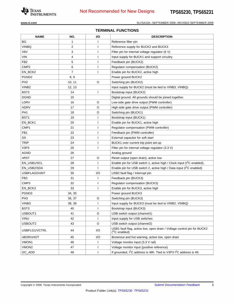
TERMINAL FUNCTIONSNAME NO. I/O DESCRIPTION
BG 1 I Reference filter pinVINBQ 2 I Reference supply for BUCK2 and BUCK3V6V 3 I Filter pin for internal voltage regulator (6 V)VIN 4 I Input supply for BUCK1 and support circuitryFB2 5 I Feedback pin (BUCK2)CMP2 6 I Regulator compensation (BUCK2)EN_BCK2 7 I Enable pin for BUCK2, active highPGND2 8, 9 Power ground BUCK2PH2 10, 11 O Switching pin (BUCK2)VINB2 12, 13 Input supply for BUCK2 (must be tied to VINB3, VINBQ)BST2 14 I Bootstrap input (BUCK2)DGND 15 Digital ground. All grounds should be joined together.LDRV 16 O Low-side gate drive output (PWM controller)HDRV 17 O High-side gate drive output (PWM controller)PH1 18 O Switching pin (BUCK1)BST1 19 I Bootstrap input (BUCK1)EN_BCK1 20 I Enable pin for BUCK1, active highCMP1 21 I Regulator compensation (PWM controller)FB1 22 I Feedback pin (PWM controller)SS 23 I External capacitor for soft startTRIP 24 I BUCK1 over current trip point set-upV3P3 25 I Filter pin for internal voltage regulator (3.3 V)AGND 26 Analog groundnRST 27 O Reset output (open drain), active lowEN_USB1/SCL 28 I Enable pin for USB switch 1, active high / Clock input (I2C enabled).EN_USB2/SDA 29 I Enable pin for USB switch 2, active high / Data input (I2C enabled)USBFLAG2/nINT 30 I/O USB2 fault flag / Interrupt pinFB3 31 I Feedback pin (BUCK3)CMP3 32 I Regulator compensation (BUCK3)EN_BCK3 33 I Enable pin for BUCK3, active highPGND3 34, 35 Power ground BUCK3PH3 36, 37 O Switching pin (BUCK3)VINB3 38, 39 I Input supply for BUCK3 (must be tied to VINB2, VINBQ)BST3 40 I Bootstrap input (BUCK3)USBOUT1 41 O USB switch output (channel1)VINU 42 I Input supply for USB switchesUSBOUT2 43 O USB switch output (channel2)
USB1 fault flag, active low, open drain / Voltage control pin for BUCK2USBFLG1/VCTRL 44 I/O (I2C enabled)nBOR/nHOT 45 I/O Brownout and hot warning, active low, open drainVMON1 46 I Voltage monitor input (3.3 V rail)VMON2 47 I Voltage monitor input (positive reference)I2C_ADD 48 I If grounded, I2C address is 48h. Tied to V3P3 I2C address is 49.
Copyright © 2009, Texas Instruments Incorporated Submit Documentation Feedback 3
Product Folder Link(s): TPS65230 TPS65231
Not Recommended for New Designs

BG
VINBQ
V6V
VIN
FB2
CMP2
EN_BCK2
PGND2
1
2
3
4
5
6
7
8
PGND2
PH2
PH2
VINB2
VINB2
BST2
DGND
LDRV
9
10
11
12
13
14
15
16
HDRV
PH1
BST1
EN_BCK1
CMP1
FB1
SS
TRIP
17
18
19
20
21
22
23
24
I2C_ADD
VMON2
VMON1
nBOR/nHOT
USBFLG1/VCTRL
USBOUT2
VINU
USBOUT1
48
47
46
45
44
43
42
41
BST3
VINB3
VINB3
PH3
PH3
PGND3
USBFLG2/nINT
PGND3
40
39
38
37
36
35
34
33 EN_BCK3
CMP3
FB3
EN_USB2/SDA
EN_USB1/SCL
nRST
AGND
V3P3
32
31
30
29
28
27
26
25
DCA HTSSOP PACKAGE
(TOP VIEW)
ABSOLUTE MAXIMUM RATINGS (1) (2)
TPS65230, TPS65231
SLVSA10A–SEPTEMBER 2009–REVISED SEPTEMBER 2009.................................................................................................................................... www.ti.com
over operating free-air temperature range (unless otherwise noted)
Input voltage range at VIN –0.3 to 25 VInput voltage range at VINB, VINBQ, VINU –0.3 to 7.0 VVoltage range at INT –0.3 to 7.0 VVoltage range at EN_BCK1, EN_BCK2, EN_BCK3, EN_USB1/SCL, EN_USB2/SDA, –0.3 to 3.6 VnRST, USBFLG1/VCTRL2, USBFLG2/VCTRL3Voltage on HDRV, BST1 –0.3 to 31 VVoltage on PH1 –0.3 to 24 VVoltage on FB1, CMP1, FB2, CMP2, FB3, CMP3 –0.3 to 3.6 VVoltage on PH2, PH3, LDRV –0.3 to 7.0 VVoltage on BST2, BST3 –0.3 to 15V VVoltage on VMON1, VMON2, VMON3 –0.3 to 3.6 VOutput Current BUCK2, BUCK3 3.8 APeak output current Internally limited
Human body model (HBM) 2 kESD rating V
Charged device model (CDM) 500θJA Thermal Resistance – Junction to ambient (3) 25 °C/W
Continuous total power dissipation 55°C (3) no thermal warning 2.6 WTJ Operating virtual junction temperature range 0 to 150 °CTA Operating ambient temperature range 0 to 85 °CTSTG Storage temperature range –65 to 150 °C
(1) Stresses beyond those listed under "absolute maximum ratings" may cause permanent damage to the device. These are stress ratingsonly, and functional operation of the device at these or any other conditions beyond those indicated under "recommended operatingconditions" is not implied. Exposure to absolute–maximum–rated conditions for extended periods may affect device reliability.
(2) All voltage values are with respect to network ground terminal.(3) Using JEDEC 51-5 (High K) board. This is based on standard 48DCA package, 4 layers, top/bottom layer: 2 oz Cu, inner layer: 1 oz Cu.
Board size: 114.3 x 76.2 mm (4.5 x 3 inches), board thickness: 1.6 mm (0.0629 inch).
4 Submit Documentation Feedback Copyright © 2009, Texas Instruments Incorporated
Product Folder Link(s): TPS65230 TPS65231
Not Recommended for New Designs

RECOMMENDED OPERATING CONDITIONS
ELECTRICAL CHARACTERISTICS
TPS65230, TPS65231
www.ti.com .................................................................................................................................... SLVSA10A–SEPTEMBER 2009–REVISED SEPTEMBER 2009
over operating free-air temperature range (unless otherwise noted)
MIN NOM MAX UNITInput voltage range at VIN 10.8 12 22 VInput voltage range at VINU 4.75 5.5 VInput voltage range at VINB 4.75 6.1Voltage range, EN_BCK1, EN_BCK2, EN_BCK3, EN_USB1/SCL, EN_USB2/SDA, 3.3 VnRST, USBFLG1/VCTRL2, USBFLG2/VCTRL3 pinsInput voltage, nRST pin 3.3 VVoltage range, INT pin (I2C disabled) 5.4 6.6 VVoltage range, INT pin (I2C enabled) 3.3 V
TA Ambient operating temperature 50 °C
VIN = 12 V ±5%, VINB2, VINB3 = 5 V ±5%, VINU = 5 V ±5% TJ = 0°C to 150°C, unless otherwise noted.
PARAMETER TEST CONDITIONS MIN TYP MAX UNITINPUT VOLTAGEVIN Input supply voltage 10.8 12 22 V
VIN rising 10.8VBOR Brown Out Reset threshold V
VIN falling 9.3VIN rising 10.8
UVLO VIN UVLO threshold – VIN (main supply) VVIN falling 4.7VINB rising 4.75UVLO threshold – VINBUVLO VINB V(BUCK2/BUCK3 supply) VINB falling 4.25VINU rising 4.4
UVLO VINU UVLO threshold – VINU (USB supply) VVINU falling 3.8
INPUT CURRENTAll regulators/USB switchesICCQ Input supply current 4 mAdisabled
LOGIC INPUT LEVEL (SCL, SDA, INT, VCTRL2, VCTRL3)VIH Input high level 1.2 VVIL Input low level 0.4 VVI2C_disable I2C disable voltage (INT) 4 VBUCK ENABLE INPUTS (EN_BCK1,2,3)VEN Enable threshold 1.2 VVENHYS Enable voltage hysteresis 100 mVIPULLUP Pull-up current tEN = 0.2 ms/nF 6 uARD Discharge resistor 1 kΩtD Discharge time Power-up 5 msI2C ENABLE THRESHOLD (INT pin)
I2C enabled if pull-up resistorVINTTH I2C enable threshold is connected to a value 4.8 V
above thresholdLOGIC OUTPUT LEVEL(SDA, INT, nRST, USBFLG1, USBFLG2 )OL Output low level IOUT = 3 mA through pull-up 0.3 0.4 VPWM CONTROLLER (BUCK1)VOUT Output voltage range (1) 3.3 6.1 VPG Power good threshold VOUT rising 95 %
(1) Output voltage range is limited by the minimum and maximum duty cycle. VOUT(min) ~ d(min) x VINPUT and VOUT(max) ~ d(max) xVINPUT.
Copyright © 2009, Texas Instruments Incorporated Submit Documentation Feedback 5
Product Folder Link(s): TPS65230 TPS65231
Not Recommended for New Designs

TPS65230, TPS65231
SLVSA10A–SEPTEMBER 2009–REVISED SEPTEMBER 2009.................................................................................................................................... www.ti.com
ELECTRICAL CHARACTERISTICS (continued)VIN = 12 V ±5%, VINB2, VINB3 = 5 V ±5%, VINU = 5 V ±5% TJ = 0°C to 150°C, unless otherwise noted.
PARAMETER TEST CONDITIONS MIN TYP MAX UNITUVD Under voltage detect VOUT falling 75 %VFB Feedback voltage –2% 0.804 2% VLDRV High and low side drive voltage No load 6 VHDRVR_ONLDRV Low side ON resistance 8 ΩR_OFFLDRV Low side OFF resistance 1 ΩR_ONHDRV High side ON resistance 20 ΩR_OFFHDRV High side OFF resistance 1 Ωd Duty cycle (2) 20 80 %AMOD Modulator gain 12fSW Switching frequency 500 kHz
Current source for setting OCP tripITRIP TA = 25°C 10 µApointTCTRIP Temperature coefficient of ITRIP 3700 ppm/°CRTRIP Current-limit setting resistor 80 250 kWCOUT Output capacitance 22 (3) 47 µFL Nominal Inductance Recommended 4.7 µHBUCK2VOUT Output voltage range (4) 0.9 3.3 VPG Power good threshold VOUT rising 95 %UVD Under voltage detect VOUT falling 75 %VFB Feedback voltage – 2% 0.804 2% VIOUT Output current 3000 mAη Efficiency IO = 2 A, VOUT = 3.3V 95 %
Low-side MOSFET On resistance 32RDS(ON) VIN12V = 12 V mΩ
High-side MOSFET On resistance 36ILIMIT Switch current limit 5 A
Current limit accuracy –30 30 %Line regulation - DC VINB = 4.75 V - 6.1 V,VLINEREG 1 %ΔVOUT/ΔVINB IOUT = 1 ALoad regulation - DCVLOADREG IOUT = 10 – 90% IOUT,MAX 0.5 %/AΔVOUT/ΔIOUT
Feedback resistor toleranceVOUTTOL DC set tolerance –2 2 %not includedd Duty cycle (5) 15 85 %AMOD Modulator gain 5fSW Switching frequency 1 MHzCOUT Output capacitance 10 (3) 47 µFESR Capacitor ESR 50 mWL Nominal inductance 2.2 µHBUCK3VOUT Output voltage range (4) 0.9 3.3 VPG Power good threshold VOUT rising 95 %UVD Under voltage detect VOUT falling 75 %
(2) Performance outside these limits is not guaranteed.(3) Absolute value. User should make allowances for tolerance and variations due to component selection.(4) Output voltage range is limited by the minimum and maximum duty cycle. VOUT(min) ~ d(min) x VINPUT and VOUT(max) ~ d(max) x
VINPUT.(5) Performance outside these limits is not guaranteed.
6 Submit Documentation Feedback Copyright © 2009, Texas Instruments Incorporated
Product Folder Link(s): TPS65230 TPS65231
Not Recommended for New Designs
TPS65230, TPS65231
www.ti.com .................................................................................................................................... SLVSA10A–SEPTEMBER 2009–REVISED SEPTEMBER 2009
ELECTRICAL CHARACTERISTICS (continued)VIN = 12 V ±5%, VINB2, VINB3 = 5 V ±5%, VINU = 5 V ±5% TJ = 0°C to 150°C, unless otherwise noted.
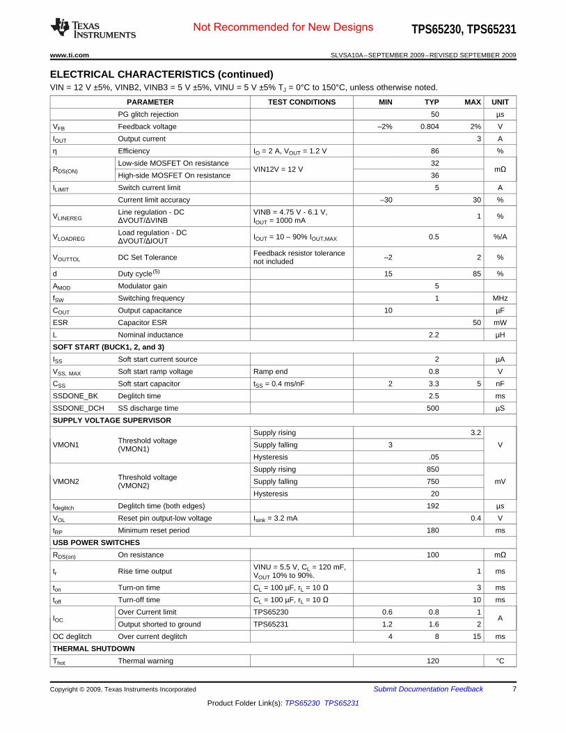
PARAMETER TEST CONDITIONS MIN TYP MAX UNITPG glitch rejection 50 µs
VFB Feedback voltage –2% 0.804 2% VIOUT Output current 3 Aη Efficiency IO = 2 A, VOUT = 1.2 V 86 %
Low-side MOSFET On resistance 32RDS(ON) VIN12V = 12 V mΩ
High-side MOSFET On resistance 36ILIMIT Switch current limit 5 A
Current limit accuracy –30 30 %Line regulation - DC VINB = 4.75 V - 6.1 V,VLINEREG 1 %ΔVOUT/ΔVINB IOUT = 1000 mALoad regulation - DCVLOADREG IOUT = 10 – 90% IOUT,MAX 0.5 %/AΔVOUT/ΔIOUT
Feedback resistor toleranceVOUTTOL DC Set Tolerance –2 2 %not includedd Duty cycle (5) 15 85 %AMOD Modulator gain 5fSW Switching frequency 1 MHzCOUT Output capacitance 10 µFESR Capacitor ESR 50 mWL Nominal inductance 2.2 µHSOFT START (BUCK1, 2, and 3)ISS Soft start current source 2 µAVSS, MAX Soft start ramp voltage Ramp end 0.8 VCSS Soft start capacitor tSS = 0.4 ms/nF 2 3.3 5 nFSSDONE_BK Deglitch time 2.5 msSSDONE_DCH SS discharge time 500 µSSUPPLY VOLTAGE SUPERVISOR
Supply rising 3.2Threshold voltageVMON1 Supply falling 3 V(VMON1)
Hysteresis .05Supply rising 850
Threshold voltageVMON2 Supply falling 750 mV(VMON2)Hysteresis 20
tdeglitch Deglitch time (both edges) 192 µsVOL Reset pin output-low voltage Isink = 3.2 mA 0.4 VtRP Minimum reset period 180 msUSB POWER SWITCHESRDS(on) On resistance 100 mΩ
VINU = 5.5 V, CL = 120 mF,tr Rise time output 1 msVOUT 10% to 90%.ton Turn-on time CL = 100 µF, rL = 10 Ω 3 mstoff Turn-off time CL = 100 µF, rL = 10 Ω 10 ms
Over Current limit TPS65230 0.6 0.8 1IOC A
Output shorted to ground TPS65231 1.2 1.6 2OC deglitch Over current deglitch 4 8 15 msTHERMAL SHUTDOWNThot Thermal warning 120 °C
Copyright © 2009, Texas Instruments Incorporated Submit Documentation Feedback 7
Product Folder Link(s): TPS65230 TPS65231
Not Recommended for New Designs

SUPPLY VOLTAGE SUPERVISOR (SVS)
nRST
Hysteresis
min 180ms
Time
VM
ON
x
USB POWER SWITCHES
TPS65230, TPS65231
SLVSA10A–SEPTEMBER 2009–REVISED SEPTEMBER 2009.................................................................................................................................... www.ti.com
ELECTRICAL CHARACTERISTICS (continued)VIN = 12 V ±5%, VINB2, VINB3 = 5 V ±5%, VINU = 5 V ±5% TJ = 0°C to 150°C, unless otherwise noted.
PARAMETER TEST CONDITIONS MIN TYP MAX UNITTtrip Thermal S/D trip point 160 °CThyst Thermal S/D hysteresis 20 °C
The supply voltage supervisor monitors two inputs, VMON1 and VMON2, and generates a reset pulse of at least180-ms length when one or more supplies fall below their respective thresholds. All inputs are deglitched for veryshort dips on the supplies. The reference values for VMON1 is specified for monitoring a 3.3-V rail without theneed of external components. The reference for VMON2 is set to monitor arbitrary supply voltages and requireresistor dividers at the inputs.
Please note that the reset signal generated by the SVS is for external use only and has no impact on the powerrails or USB switches of the TPS65230 and TPS65231.
Figure 1. Supply Voltage Supervisor Reset Generation
The TPS65230 and TPS65231 provide two power-distribution switches intended for applications where heavycapacitive loads and short-circuits are likely to be encountered. Gate drive is provided by an internal regulator.Each switch is controlled by a logic enable input or, when I2C interface is enabled, switches are controlledthrough EN_USBx bits of the ENABLE register.
When the output load exceeds the current-limit threshold or a short is present, the device limits the output currentto a safe level by switching into a constant-current mode, pulling the USBFAULTx output low. When continuousheavy overloads and short-circuits increase the power dissipation in the switch, causing the junction temperatureto rise, a thermal protection circuit shuts off the switches when a thermal warning condition occurs to preventdamage. Recovery from a thermal warning is automatic once the device has cooled sufficiently. Internal circuitryensures that the switch remains off until valid input voltage is present.
8 Submit Documentation Feedback Copyright © 2009, Texas Instruments Incorporated
Product Folder Link(s): TPS65230 TPS65231
Not Recommended for New Designs

POWER-UP SEQUENCING
V3p3V3p3
(1)
(2)
EN_BCKxBUCK ENABLE
6uA
Enable
Threshold
BUCK A
Enable
BUCK B
Enable
BUCK C
Enable
V(E
Np
in)
Time
Delay time = 0.2ms/nF
1.2V
(1) Connect EN_BCKx pin to V3P3 to follow the default power-up sequence or(2) Connect a capacitor from EN_BCKx to GND to generate a custom power-up sequence.
OVER CURRENT PROTECTION
I =LIM
R ITRIP TRIP·
10 · RDS(ON)
¾
(1)
TPS65230, TPS65231
www.ti.com .................................................................................................................................... SLVSA10A–SEPTEMBER 2009–REVISED SEPTEMBER 2009
ON/OFF control and power sequencing of the three buck regulators is controlled through EN_BCK1, EN_BCK2,and EN_BCK3 enable pins. Each pin is internally connected to a 6-µA constant-current source and monitored bya comparator with Schmitt trigger input with defined threshold. Connecting EN_BCKn pin to ground disablesBUCKn and connecting EN_BCKn to V3P3 will enable the respective buck without delay. If more than one buckenable pin is connected to V3P3 the default startup sequence is BUCK1, BUCK2, BUCK3 and the minimumstartup delay between rails is the soft-start time (typical 1.5 ms) plus 1 ms.
To create a startup-sequence different from the default, capacitors are connected between the EN_BUCKn pinsand ground. At power-up the capacitors are first discharged and then charged to V3P3 level by internal currentsources (6 µA typical) creating a constant-slope voltage ramp. A regulator is enabled when its EN pin voltagecrosses the enable threshold (typical 1.2 V). A delay of 0.2 ms is generated for each 1-nF of capacitanceconnected to the enable pin. If two enable pins are pulled high while the third regulator is starting up, the defaultsequence will be applied to enable the remaining two regulators. To override default power-up sequence it isrecommended that delay times differ by more than the soft-start time (typical 1.3 ms) plus 1 ms.
In I2C mode regulators can also be enabled by setting their respective EN bits in the ENABLE register. The samestartup-time limitations and arbitration rules apply in I2C mode as described above.
Figure 2. Customizing the Power-Up Sequence
Over current protection (OCP) for BUCK1 is achieved by comparing the drain-to-source voltage of the low-sideMOSFET to a set-point voltage, which is defined by both the internal current source, ITRIP, and the externalresistor connected between the TRIP pin and ground. Over current threshold is calculated as Equation 1.
ITRIP has a typical value of 10 µA at 25°C and a temperature coefficient of 3700 ppm/°C to compensate thetemperature dependency of the MOS RDS(ON). The TPS65230 and TPS65231 support cycle-by-cycle over currentlimiting control which means that the controller compares the drain-to-source voltage of the low-side FET to theset-point voltage once per switching cycle and blanks out the next switching cycle if an over-current condition isdetected. If in the following cycle over current condition is detected again, the controller blanks out 2, then 4, 8,and up to 16 cycles before turning on the high-side driver again. In an over current condition the current to theload exceeds the current to the output capacitor thus the output voltage will drop, and eventually cross the under
Copyright © 2009, Texas Instruments Incorporated Submit Documentation Feedback 9
Product Folder Link(s): TPS65230 TPS65231
Not Recommended for New Designs
SOFT START
BROWNOUT MONITOR (BOR)
TPS65230, TPS65231
SLVSA10A–SEPTEMBER 2009–REVISED SEPTEMBER 2009.................................................................................................................................... www.ti.com
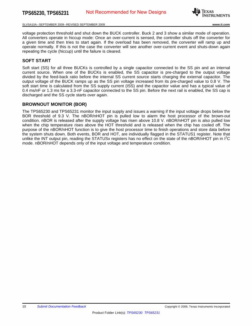
voltage protection threshold and shut down the BUCK controller. Buck 2 and 3 show a similar mode of operation.All converters operate in hiccup mode: Once an over-current is sensed, the controller shuts off the converter fora given time and then tries to start again. If the overload has been removed, the converter will ramp up andoperate normally. If this is not the case the converter will see another over-current event and shuts-down againrepeating the cycle (hiccup) until the failure is cleared.
Soft start (SS) for all three BUCKs is controlled by a single capacitor connected to the SS pin and an internalcurrent source. When one of the BUCKs is enabled, the SS capacitor is pre-charged to the output voltagedivided by the feed-back ratio before the internal SS current source starts charging the external capacitor. Theoutput voltage of the BUCK ramps up as the SS pin voltage increased from its pre-charged value to 0.8 V. Thesoft start time is calculated from the SS supply current (ISS) and the capacitor value and has a typical value of0.4 ms/nF or 1.3 ms for a 3.3-nF capacitor connected to the SS pin. Before the next rail is enabled, the SS cap isdischarged and the SS cycle starts over again.
The TPS65230 and TPS65231 monitor the input supply and issues a warning if the input voltage drops below theBOR threshold of 9.3 V. The nBOR/nHOT pin is pulled low to alarm the host processor of the brown-outcondition. nBOR is released after the supply voltage has risen above 10.8 V. nBOR/nHOT pin is also pulled lowwhen the chip temperature rises above the HOT threshold and is released when the chip has cooled off. Thepurpose of the nBOR/nHOT function is to give the host processor time to finish operations and store data beforethe system shuts down. Both events, BOR and HOT, are individually flagged in the STATUS1 register. Note thatunlike the INT output pin, reading the STATUSx registers has no effect on the state of the nBOR/nHOT pin in I2Cmode. nBOR/nHOT depends only of the input voltage and temperature condition.
10 Submit Documentation Feedback Copyright © 2009, Texas Instruments Incorporated
Product Folder Link(s): TPS65230 TPS65231
Not Recommended for New Designs

nBOR/nHOT
VIN (12 V)
10.8V
9.3V
4.8V
UVLO (internal signal )
Available time for controlled
shutdown of System
Under Voltage Lock Out(UVLO)
disables all output rails and USB
Sys
tem
resu
mes
no
rmal
op
era
tion
.
Time
Thermal Shutdown (TSD)
Thermal warning (HOT )
nBOR/nHOT
Available time for controlled
shutdown of System
160C
130CNOTE: All rails are shutdownwhen temperature exceeds TSDthreshold. System recoversautomatcally when IC has cooleddown to TSD- TSDHYSTERESIS.
Temperature
UNDER VOLTAGE LOCKOUT (UVLO)
TPS65230, TPS65231
www.ti.com .................................................................................................................................... SLVSA10A–SEPTEMBER 2009–REVISED SEPTEMBER 2009
Figure 3. Brownout Monitoring
TPS65230 and TPS65231 monitors VIN, VINB, and VINU pin voltages and will disable one or more power pathsdepending on the current use condition:• If VIN drops below 9.3 V, both USB power paths are disabled and the nBOR/nHOT output pin is pulled low.• If VIN drops below 4.7 V, BUCK1, 2, and 3 are disabled.• If VINB drops below 4.25 V and either BUCK2 or BUCK3 are enabled, all three output rails are disabled.• If VINU drops below 3.9V and either USB1 or USB2 are enabled, both USB switches are disabled.
UVLO state is not latched and the system recovers as soon as the input voltage rises above its respectivethreshold. All three BUCK_ENx pins are discharged and remain discharged during UVLO to ensure proper powersequencing when the system recovers.
In I2C mode the EN_BUCKx and EN_USBx bits of the ENABLE register are reset in an UVLO event and interruptis issued. To re-enable the output supplies, the respective EN_BUCKx bits have to be set through the I2Cinterface or the BUCK_ENx pins have to be pulled high. To re-enable the USB power switches in I2C mode, theEN_USBx bits of the ENABLE register have to be set through the I2C interface.
Copyright © 2009, Texas Instruments Incorporated Submit Documentation Feedback 11
Product Folder Link(s): TPS65230 TPS65231
Not Recommended for New Designs

THERMAL SHUTDOWN (TSD)
LOOP COMPENSATION
3.3-V REGULATOR
6-V REGULATOR
USER SELECTABLE SERIAL INTERFACE
TPS65230, TPS65231
SLVSA10A–SEPTEMBER 2009–REVISED SEPTEMBER 2009.................................................................................................................................... www.ti.com
TPS65230x monitors junction temperature and will disable all power paths (BUCK1-3, USB1 and 2) if junctiontemperature rises above the specified trip point. nBOR/nHOT pin will be pulled low if the temperature approachesthe TSD trip point within 40°C. In I2C mode the device will also issue an interrupt and set the HOT bit inSTATUS1 register. The system recovers as soon as the temperature falls below the falling-edge triptemperature. All three BUCK_ENx pins are discharged and remain discharged during TSD to ensure properpower sequencing when the system recovers.
In I2C mode the EN_BUCKx and EN_USBx bits of the ENABLE register are reset in a TSD event and interrupt isissued. To re-enable the output supplies the respective EN_BUCKx bits have to be set through the I2C interfaceor the BUCK_ENx pins have to be pulled high. To re-enable the USB power switches in I2C mode, the EN_USBxbits of the ENABLE register have to be set through the I2C interface.
All three BUCKs are voltage mode converters designed to be stable with ceramic capacitors. Refer toComponent Selection Procedure section for calculating feedback components.
The TPS6532x has a built-in 3.3-V regulator for powering internal circuitry. The 3.3-V rail can also be used forenabling the BUCK regulators and/or the USB switches, but is not intended for supplying any other externalcircuitry. For light loading of this rail during stand-by operation consult TI FAE.
The TPS6532x has a built-in 6-V regulator for powering internal circuitry. The 6-V rail can also be used forenabling I2C functionality by connecting the pull-up resistor on the USBFLG2/nINT pin to V6V but is not intendedfor supplying any other external circuitry. For light loading of this rail during stand-by operation consult TI FAE.
TPS65230 and TPS65231 feature an I2C slave interface which can be enabled or disabled by the user and offersadvanced control and diagnostic features. I2C control is enabled when the pull-up resistor on the USBFLG2/nINTpin is connected to a supply voltage > 4.5 V and is disabled otherwise. When disabled, BUCK1, 2, 3, and USB1,2 are controlled through their respective enable pins. When the I2C interface is enabled, USB1 and USB2 arecontrolled through the serial interface and BUCK1, 2, and 3 are controlled either through the serial interface ortheir respective enable pins. In addition, the USBFLG1/VCTRL pin is reconfigured when I2C is enabled to offeroutput voltage control for BUCK2 and BUCK3.
I2C operation offers brownout and thermal shutdown warning, thermal shut down flag, power-good andunder-voltage indicator for BUCK1-3 and USB fault indicator for both USB switches. Whenever a fault isdetected, the associated status bit in the STATUS1 and 2 registers are set and the INT pin is pulled low.Reading of the STATUS1 and 2 registers resets the flag bits and INT pin is released after all flags have beenreset. Note that in I2C mode the nINT pin is active high with voltage swing of > 3.3 V. To invert the signal andshift the voltage level down to an I/O compatible level, connect the circuit shown in Figure 5 to the USBFL2/nINTpin.
INT Dependent Device Pin ConfigurationPIN NO. DEVICE PIN USBFLG2/INT CONNECTED TO V6V (1) USBFLG2/INT CONNECTED TO 3.3V (1)
30 USBFLG2/nINT nINT Error flag for USB switch 228 EN_USB1/SCL SCL (Clock) Enable pin for USB switch 129 EN_USB2/SDA SDA (Data) Enable pin for USB switch 244 USBFLG1/VCTRL Voltage control input for BUCK2 and 3 Error flag for USB switch 1
(1) Via pull-up resistor
12 Submit Documentation Feedback Copyright © 2009, Texas Instruments Incorporated
Product Folder Link(s): TPS65230 TPS65231
Not Recommended for New Designs

VBCK3[1:0]
00 – 0%
01 – 5%
10 – 10%
11 – 15%
VBCK2[1:0]
00 – 0%
01 – 5%10 – 10%
11 – 15%
VBUCK3
VBUCK2
VBUCK1
VCTRL pinor VCTRL bit
Time
2222A
10K
47.5K
4.7K
To uC
USBFLG2/nINT
V6V 3.3V
I2C BUS OPERATION
G3 G2 A1 A0 R/nW ACKStart G1 G0 A2 S7 S6 S2 S1S5 S4 S3 S0 ACK D7 D6 D2 D1D5 D4 D3 D0 ACK Stop
Slave Address + R/nW Sub Address Data
TPS65230, TPS65231
www.ti.com .................................................................................................................................... SLVSA10A–SEPTEMBER 2009–REVISED SEPTEMBER 2009
I2C operation also offers output voltage adjustment options for BUCK2 and BUCK3. This is feature is useful toreduce power dissipation in the system by lowering the supply voltages when the system is in idle state. Outputvoltage can be scaled down by 5, 10 and 15% depending on the VBCKn[1:0] bit settings in the VADJUSTregister. Settings are activated when the USBFLG1/VCTRL pin is pulled high and are deactivated when the pin ispulled low. This allows for fast output voltage transition without involvement of the I2C interface. Alternatively thesettings can be activated by setting the the VCTRLx bits of the ENABLE register.
Figure 4. BUCK2 and BUCK3 Output Voltages
Figure 5. Circuit for Level-Shifting and Inverting nINT Signal
The TPS65230 hosts a slave I2C interface that supports data rates up to 400 kbit/s and auto-incrementaddressing and is compliant to I2C standard 3.0.
Figure 6. Subaddress in I2C Transmission
Start — Start condition
G(3:0) — Group ID: 1001
A(2:0) — Device address: 000
R/nW — Read/not write select bit
Copyright © 2009, Texas Instruments Incorporated Submit Documentation Feedback 13
Product Folder Link(s): TPS65230 TPS65231
Not Recommended for New Designs
START CONDITION
. . .
ACKNOWLEDGE STOP CONDITION
SCL
SDA
1 2 3 4 5 6 7 8 9. . .
P S S P
t S( D AT ) t S (S TA ) t S (S TO )tH I G Ht H (D A T )
t H (S TA )
t LO W t r( t F
t H (S T A)
t (B U F)
S C L
S D A
TPS65230, TPS65231
SLVSA10A–SEPTEMBER 2009–REVISED SEPTEMBER 2009.................................................................................................................................... www.ti.com
ACK — Acknowledge
S(7:0) — Subaddress: defined per register map
D(7:0) — Data: data to be loaded into the device
Stop — Stop condition
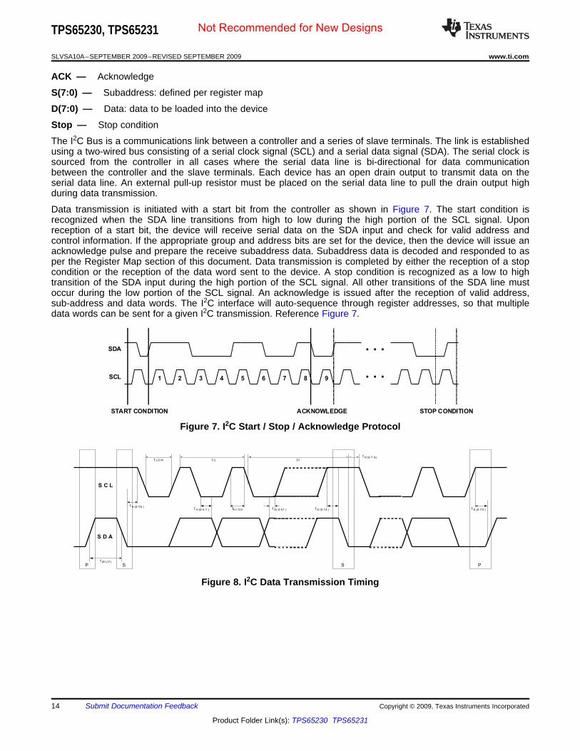
The I2C Bus is a communications link between a controller and a series of slave terminals. The link is establishedusing a two-wired bus consisting of a serial clock signal (SCL) and a serial data signal (SDA). The serial clock issourced from the controller in all cases where the serial data line is bi-directional for data communicationbetween the controller and the slave terminals. Each device has an open drain output to transmit data on theserial data line. An external pull-up resistor must be placed on the serial data line to pull the drain output highduring data transmission.
Data transmission is initiated with a start bit from the controller as shown in Figure 7. The start condition isrecognized when the SDA line transitions from high to low during the high portion of the SCL signal. Uponreception of a start bit, the device will receive serial data on the SDA input and check for valid address andcontrol information. If the appropriate group and address bits are set for the device, then the device will issue anacknowledge pulse and prepare the receive subaddress data. Subaddress data is decoded and responded to asper the Register Map section of this document. Data transmission is completed by either the reception of a stopcondition or the reception of the data word sent to the device. A stop condition is recognized as a low to hightransition of the SDA input during the high portion of the SCL signal. All other transitions of the SDA line mustoccur during the low portion of the SCL signal. An acknowledge is issued after the reception of valid address,sub-address and data words. The I2C interface will auto-sequence through register addresses, so that multipledata words can be sent for a given I2C transmission. Reference Figure 7.
Figure 7. I2C Start / Stop / Acknowledge Protocol
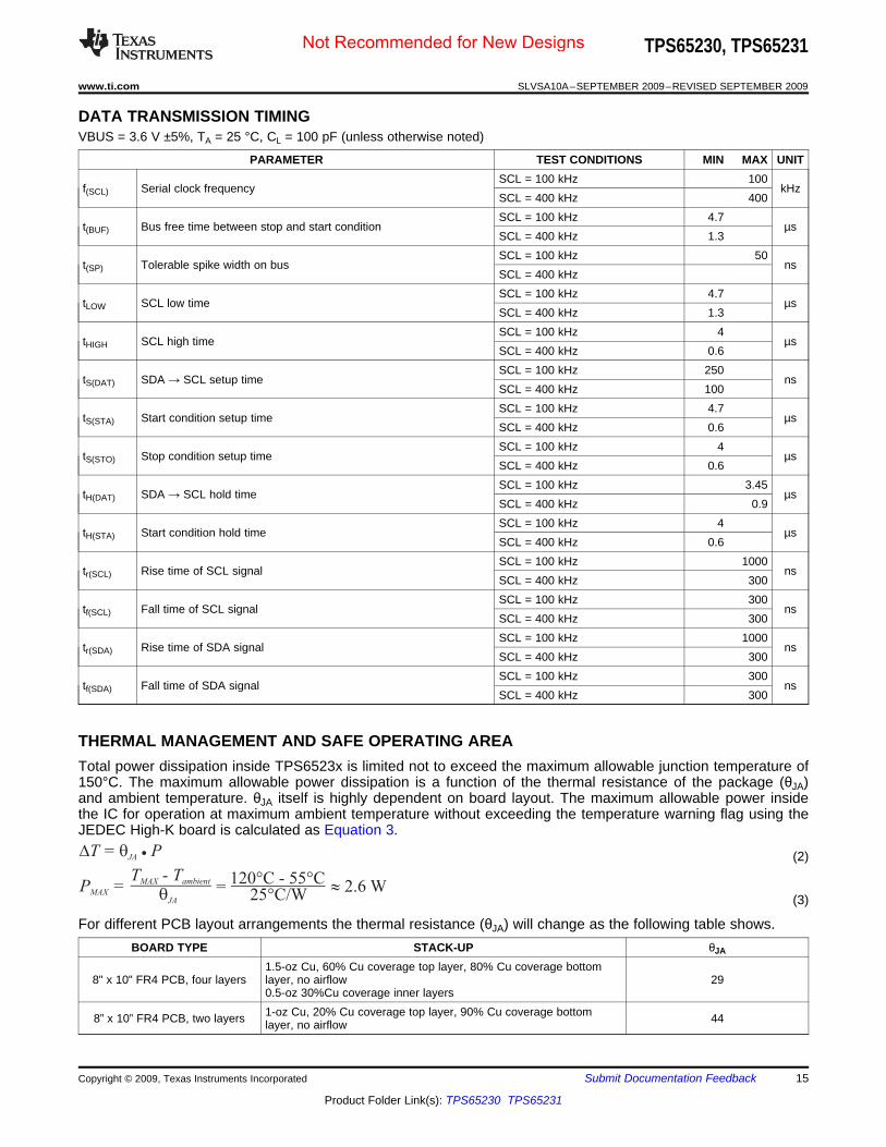
Figure 8. I2C Data Transmission Timing
14 Submit Documentation Feedback Copyright © 2009, Texas Instruments Incorporated
Product Folder Link(s): TPS65230 TPS65231
Not Recommended for New Designs
DATA TRANSMISSION TIMING
THERMAL MANAGEMENT AND SAFE OPERATING AREA
D qT = PJA
· (2)
P =MAX
T - TMAX ambient
qJA
¾ =120°C - 55°C¾
25°C/W» 2.6 W
(3)
TPS65230, TPS65231
www.ti.com .................................................................................................................................... SLVSA10A–SEPTEMBER 2009–REVISED SEPTEMBER 2009
VBUS = 3.6 V ±5%, TA = 25 °C, CL = 100 pF (unless otherwise noted)
PARAMETER TEST CONDITIONS MIN MAX UNITSCL = 100 kHz 100
f(SCL) Serial clock frequency kHzSCL = 400 kHz 400SCL = 100 kHz 4.7
t(BUF) Bus free time between stop and start condition µsSCL = 400 kHz 1.3SCL = 100 kHz 50
t(SP) Tolerable spike width on bus nsSCL = 400 kHzSCL = 100 kHz 4.7
tLOW SCL low time µsSCL = 400 kHz 1.3SCL = 100 kHz 4
tHIGH SCL high time µsSCL = 400 kHz 0.6SCL = 100 kHz 250
tS(DAT) SDA → SCL setup time nsSCL = 400 kHz 100SCL = 100 kHz 4.7
tS(STA) Start condition setup time µsSCL = 400 kHz 0.6SCL = 100 kHz 4
tS(STO) Stop condition setup time µsSCL = 400 kHz 0.6SCL = 100 kHz 3.45
tH(DAT) SDA → SCL hold time µsSCL = 400 kHz 0.9SCL = 100 kHz 4
tH(STA) Start condition hold time µsSCL = 400 kHz 0.6SCL = 100 kHz 1000
tr(SCL) Rise time of SCL signal nsSCL = 400 kHz 300SCL = 100 kHz 300
tf(SCL) Fall time of SCL signal nsSCL = 400 kHz 300SCL = 100 kHz 1000
tr(SDA) Rise time of SDA signal nsSCL = 400 kHz 300SCL = 100 kHz 300
tf(SDA) Fall time of SDA signal nsSCL = 400 kHz 300
Total power dissipation inside TPS6523x is limited not to exceed the maximum allowable junction temperature of150°C. The maximum allowable power dissipation is a function of the thermal resistance of the package (θJA)and ambient temperature. θJA itself is highly dependent on board layout. The maximum allowable power insidethe IC for operation at maximum ambient temperature without exceeding the temperature warning flag using theJEDEC High-K board is calculated as Equation 3.
For different PCB layout arrangements the thermal resistance (θJA) will change as the following table shows.BOARD TYPE STACK-UP θJA
1.5-oz Cu, 60% Cu coverage top layer, 80% Cu coverage bottom8" x 10" FR4 PCB, four layers layer, no airflow 29
0.5-oz 30%Cu coverage inner layers1-oz Cu, 20% Cu coverage top layer, 90% Cu coverage bottom8” x 10” FR4 PCB, two layers 44layer, no airflow
Copyright © 2009, Texas Instruments Incorporated Submit Documentation Feedback 15
Product Folder Link(s): TPS65230 TPS65231
Not Recommended for New Designs

0
0.5
1
1.5
2
2.5
3
3.5
0 0.5 1 1.5 2 2.5 3 3.5
Current from BUCK2 [A] @ 1.2V or less
Curr
en
tfr
om
BUC
K3
[A]@
3.3
V
Safe Operating Area
0
0.5
1
1.5
2
2.5
3
3.5
0 0.5 1 1.5 2 2.5 3 3.5
Current from BUCK2 [A] @ 1.8V
Curre
nt
from
BU
CK
3[A
]@
3.3
V
Safe Operat ing Area
0
0.5
1
1.5
2
2.5
3
3.5
0 0.5 1 1.5 2 2.5 3 3.5
Current from BUCK2 [A] @ 2.5V
Cu
rren
tfr
om
BU
CK
3[A
]@
3.3
V
Safe Operating Area
For any voltage / current comination inside the shaded area, the dissipated power inside the chip is below the allowable
maximum. The examples assume T < 60°C, = 90% and < 44°C/W.ambient JAh q
COMPONENT SELECTION PROCEDURE
TPS65230, TPS65231
SLVSA10A–SEPTEMBER 2009–REVISED SEPTEMBER 2009.................................................................................................................................... www.ti.com
A minimum of two layers of 1-oz Cu with 20% Cu coverage on the top and 90% coverage on the bottom and theuse of thermal vias to connect the thermal pad to the bottom layer is recommended. Note that the maximumallowable power inside the device will depend on the board layout. For recommendations on board layout forthermal management using TPS6523x consult your TI field application engineer.
In the example shown above the maximum allowable power dissipation for the IC has been calculated. Thisfigure includes all heat sources inside the device including the power dissipated in BUCK1, BUCK2, BUCK3,USB switches, and all supporting circuitry. Power dissipated in BUCK1, USB switches (500 mA full load) , and allsupporting circuitry is approximately 0.4 W and almost independent of the application. Power dissipated inBUCK2 and BUCK3 depends on the output voltage, output current, and efficiency of the switching converters.The following examples of safe operating area assume 90% efficiency for BUCK2 and BUCK3, 3.3-V output fromBUCK3 and 1.2-V, 1.8-V, and 2.5-V output from BUCK2, respectively.
Figure 9. Examples of Thermal Safe Operating Area for V(BUCK3) = 3.3 V and V(BUCK1) = 1.2 V, 1.8 Vand 2.5 V, Respectively
The following example illustrates the design procedure for selecting external components for the three buckconverters. The example focuses on BUCK1 but the procedure can be directly applied to BUCK2 and 3 as well.The design goal parameters are given in the table below. A list of symbol definitions is found at the end of thissection. For this example the schematic in Figure 10 will be used.
16 Submit Documentation Feedback Copyright © 2009, Texas Instruments Incorporated
Product Folder Link(s): TPS65230 TPS65231
Not Recommended for New Designs

INDUCTOR SELECTION
L =V - VIN(MAX) OUT
0.3 · IOUT
¾ ·
VOUT
VIN(MAX)
¾ ·
1¾fSW (4)
TPS65230, TPS65231
www.ti.com .................................................................................................................................... SLVSA10A–SEPTEMBER 2009–REVISED SEPTEMBER 2009
Figure 10. Sample Schematic for TPS6523x Showing Components Relevant to BUCK1PARAMETER TEST CONDITIONS MIN TYP MAX UNIT
VIN Input supply voltage 10.8 12 13.2 VVIN RIPPLE Input voltage ripple IOUT, BUCK1 = 6 A 60 mVVOUT Output Voltage 4.75 5 5.25 V
Line regulation VIN = 10.8 V to 13.2 V 25 mVLoad regulation IOUT, BUCK1 = 0 A to 6 A 25 mV
VOUT RIPPLE Output ripple IOUT, BUCK1 = 6 A 50 mVVTRANS Transient deviation IOUT, BUCK1 = 2 A to 6 A 125 mVIOUT Output current VIN = 10.8 V to 13.2 V 0 6 AfSW Switching frequency 500 kHz
For BUCK1 the recommended inductor value is 4.7 µH and for BUCK2 and 3 it is 2.2 µH. These values willprovide a good balance between ripple current, efficiency, loop bandwidth and inductor cost. The inductor istypically sized for < 30% peak-to-peak ripple current (IRIPPLE). Given this target ripple current, the requiredinductor size is calculated by Equation 4.
Solving Equation 4 with VIN(MAX) = 13.2 V, an inductor value of 3.5 µH is obtained. A standard value of 4.7 µH isselected, resulting in 1.25-A peak-to-peak ripple. The RMS current through the inductor is approximated byEquation 5.
Copyright © 2009, Texas Instruments Incorporated Submit Documentation Feedback 17
Product Folder Link(s): TPS65230 TPS65231
Not Recommended for New Designs

I =L(RMS) Ö(IL(avg)
2+ 1¾
12(I )RIPPLE
2) =Ö¾ ¾
(I )OUT
2+ 1¾
12 (I )RIPPLE
2
(5)
OUTPUT CAPACITOR SELECTION
C =OUT(MIN)
I LTRAN(MAX)
2
·
¾
(V - V ) VIN(MIN) OUT TRAN·
when < 2V VIN(MIN) OUT·
(6)
C =OUT(MIN)
I LTRAN(MAX)
2
·
¾
V VOUT TRAN·
when > 2V VIN(MIN) OUT·
(7)
ESR =MAX
V - VRIPPLE(total) RIPPLE(cap)¾
IRIPPLE
=
V -RIPPLE(total)
¾
IRIPPLE
(IRIPPLE¾
C fOUT SW·
)
(8)
PEAK CURRENT RATING OF THE INDUCTOR
I =CHARGE
V COUT OUT
·
¾T
SS (9)
I = IL(PEAK) OUT(MAX) +1¾
2I IRIPPLE CHARGE+
(10)
INPUT CAPACITOR SELECTION
TPS65230, TPS65231
SLVSA10A–SEPTEMBER 2009–REVISED SEPTEMBER 2009.................................................................................................................................... www.ti.com
Using Equation 5, the maximum RMS current in the inductor is about 6.01 A.
The selection of the output capacitor is typically driven by the output load transient response requirement. Theoutput capacitance (base) proposed is 2 x 22 µF (or 4 X 10 µF or 1 x 47 µF) ceramic, providing a good balancebetween ripple, cost and performance. Extra caps added should be electrolyte or far from base cap to haveconsiderable amount of ESR and not to affect compensation.
Equation 6 and Equation 7 estimate the output capacitance required for a given output voltage transientdeviation.
For this example, Equation 7 is used in calculating the minimum output capacitance.
Based on a 4-A load transient with a maximum 125-mV deviation (2.5% of set voltage), a minimum of 120-µFoutput capacitance is required. We choose two 22-µF ceramic capacitors and two electrolytic 47 µF in parallel fora total capacitance of 138 µF.
The output ripple is divided into two components. The first is the ripple generated by the inductor ripple currentflowing through the output capacitor’s capacitance, and the second is the voltage generated by the ripple currentflowing in the output capacitor’s ESR. The maximum allowable ESR is then determined by the maximum ripplevoltage and is approximated by Equation 8.
Based only on the 138-µF of capacitance, 1.25-A ripple current, 500-kHz switching frequency and a design goalof 50-mV ripple voltage (1% of set voltage), we calculate a capacitive ripple component of 18 mV and amaximum ESR of 25 mΩ. The X5R ceramic capacitors selected provide significantly less than 25-mΩ of ESR.
With output capacitance known, it is now possible to calculate the charging current during start-up and determinethe minimum saturation current rating of the inductor. The start-up charging current is approximated byEquation 9.
Using the TPS65230 and TPS65231’s recommended 1.3-ms soft-start time, COUT = 188 µF and VOUT = 5 V,ICHARGE is found to be 720 mA. The peak current rating of the inductor is now found by Equation 10.
For this example an inductor with a peak current rating of 7.3 A is required. Note however that the inductor willneed to withstand the current limit figure without a major reduction of its rated inductance.
The input voltage ripple is divided between capacitance and ESR. For this design, VRIPPLE(cap) = 60 mV (0.5% ofsupply) and VRIPPLE(ESR) = 30 mV (0.25% of supply). The minimum capacitance and maximum ESR areestimated by Equation 11 and Equation 12.
18 Submit Documentation Feedback Copyright © 2009, Texas Instruments Incorporated
Product Folder Link(s): TPS65230 TPS65231
Not Recommended for New Designs

C =IN(MIN)
I VLOAD OUT·
¾
V V fRIPPLE(cap) IN SW· · (11)
ESR =MAX
VRIPPLE(ESR)¾
ILOAD +1¾
2IRIPPLE (12)
I = I - I =RMS(CIN) IN(RMS) IN(avg) Ö((I )OUT
2+ 1¾
12(I )RIPPLE
2)·VOUT¾VIN
¾-
V IOUT OUT·¾
VIN (13)
BOOTSTRAP CAPACITOR
C =BOOST
20 · QGS, HSD¾
VIN(MIN) (14)
SHORT CIRCUIT PROTECTION (BUCK1 ONLY)
V = I RDS L(PEAK) DSON, LSD· (15)
R = R ITRIP DS(ON) LIM· · 106
(16)
SHORT CIRCUIT PROTECTION (BUCK2 AND 3 ONLY)
FEEDBACK LOOP DESIGN
TPS65230, TPS65231
www.ti.com .................................................................................................................................... SLVSA10A–SEPTEMBER 2009–REVISED SEPTEMBER 2009
For this design, CIN > 8 µF and ESR < 4 mΩ. The RMS current in the output capacitors is estimated byEquation 13.
With VIN = VIN(MAX), the input capacitors must support a ripple current of 1.4-A RMS. It is important to check theDC bias voltage de-rating curves to ensure the capacitors provide sufficient capacitance at the working voltage.Typically a 10-µF capacitor per converter is used. These capacitors should be placed as close as possible to theVINB2 and VINB3 pins (BUCK2 and BUCK3) and to the external MOSFET arrangement for BUCK1.
To ensure proper charging of the high-side MOSFET gate, limit the ripple voltage on the bootstrap capacitor to< 5% of the minimum gate drive voltage.
Based on the FDS6982 MOSFET with a maximum total gate charge of 26 nC, calculate a minimum of 80-nF ofcapacitance. A standard value of 220 nF is selected for BUCK1 and 100 nF for BUCK2.
The TPS65230 and TPS65231 uses the forward drop across the low-side MOSFET during the OFF time tomeasure the inductor current. The voltage drop across the low-side MOSFET is given by Equation 15.
When VIN = 10.8 V to 13.2 V, IPEAK = 7.4A for full load (6 A). Using the FDS6982 MOSFET with a RDSON,MAX at TJ= 25°C of 20 mΩ we calculate the peak voltage drop to be 148 mV. Adding a 50% margin to include inductorvariations and overload margin, the drop voltage for tip is set at 210 mV. Solving Equation 1 for RTRIP and usingITRIP = 10 µA:
We calculate a trip resistor value of 210 kΩ. Place a 1-nF capacitor parallel to R9. Please note that typical FETRDS(ON) is specified at 10 mΩ. Since we used RDSON,MAX, for setting the current limit, the actual current flowingthrough the inductor with a nominal FET can be higher than the peak current of 7.4 A before the current limitkicks in. Make sure that the chosen inductor has the correct peak current capabilities.
Current limits for BUCK2 and 3 are internally set to 5 A.
For the TPS6523x, the switching frequency and nominal output filter combination have been chosen to be0.5 MHz 4.7 µH/~40 µF for BUCK1 and 1 MHz 2.2 µH/~40 µF for BUCK2 and 3 respectively. These values wereseen as a good compromise between efficiency and small solution size. The bandwidth has been chosen to bearound 1/8th - 1/11th of the switching frequency to maximize transient response whilst retaining low noisesensitivity. As indicated before it is required that the output capacitor is ceramic and further that the very low ESRcauses it’s associated zero to be at or above the bandwidth of the converter.
Copyright © 2009, Texas Instruments Incorporated Submit Documentation Feedback 19
Product Folder Link(s): TPS65230 TPS65231
Not Recommended for New Designs

Rc
CcCroll
Comp
FB
Vout
R2
R1
Cz
R =29V R
FB· 25
¾V - V
OUT FB (17)
Other Components
TPS65230, TPS65231
SLVSA10A–SEPTEMBER 2009–REVISED SEPTEMBER 2009.................................................................................................................................... www.ti.com
The control loop for the TPS6523x has an internal mid- to high-frequency zero-pole pair to compensate theresonant pole caused by the output L-C filter. The maximum phase boost occurs at the geometric mean of thepole zero arrangement and therefore aimed to be equal to the desired bandwidth. The pole limits the gain at highfrequencies to reduce noise sensitivity and it is about 5 times higher than the zero located at ~45 kHz.
The COMP pin of the buck converters is the output of an integrator Used to get high DC accuracy. The integratoralso takes care of any offsets in the zero-pole pair amplifier and the summing comparator inside the device. Alsoa feed-forward loop is added to the attenuator circuit.
Figure 11. External Compensation Circuit
The procedure to set the integrator values is very simple (see Figure 11):1. Set the feed-forward circuit making R2 = 20 kΩ, CZ= 1 nF.2. Calculate R1 as per output voltage requirement. Select R25 between 10 kΩ and 100 kΩ. For this design
select 22.1 kΩ, 0.1% resistor for the upper side of all dividers. Next, R29 Is selected to produce the desiredoutput voltage when VFB = 0.8 V using Equation 17.
VFB = 0.8 V and R25 = 22.1 kΩ for VOUT = 5.0 V, R25 = 4.209 kΩ. The closest value 4.22 kΩ.3. Set the integrator values, RC = 20 kΩ, CC = 1 nF.4. Make Croll = 100 pf to roll-off gain at high frequencies.5. If VIN is ~20 - 24 V use 200 pF for Croll on DCDC1.
A 1-µF ceramic capacitor should be connected as close as possible to the following pins:• BG (pin 1): Bandgap reference• VIN (pin 4): Bypass capacitor (higher values are acceptable)• V6V (pin 3): Internal 6 V supply• V3P3 (pin 25): Internal 3.3 V supply
20 Submit Documentation Feedback Copyright © 2009, Texas Instruments Incorporated
Product Folder Link(s): TPS65230 TPS65231
Not Recommended for New Designs

TPS65230, TPS65231
www.ti.com .................................................................................................................................... SLVSA10A–SEPTEMBER 2009–REVISED SEPTEMBER 2009
Register Address MapREGISTER ADDRESS (HEX) NAME DEFUALT VALUE DESCRIPTION
0 00 ENABLE 0000 0000 Enable control register1 01 VADJUST 0000 0000 Voltage adjustment register2 02 STATUS1 0000 0000 Status bit register3 03 STATUS2 0000 0000 Status bit register
ENABLE Register (ENABLE), Address - 0X00HDATA BIT D7 D6 D5 D4 D3 D2 D1 D0
FIELD NAME Not used Not used VCTRL EN_BCK1 EN_BCK2 EN_BCK3 EN_USB1 EN_USB2READ/WRITE R/W R/W R/W R/W R/W R/W R/W R/W
RESET 0 0 0 0 0 0 0 0VALUE
FIELD NAME (1) BIT DEFINITIONVoltage control bit for BUCK2 and BUCK3
VCTRL 0 – Nominal output voltage1 – Enable voltage adjustment level set by VADJUST registerEnable BUCK1
EN_BCK1 0 – Disabled1 - EnabledEnable BUCK2
EN_BCK2 0 – Disabled1 - EnabledEnable BUCK3
EN_BCK3 0 – Disabled1 - EnabledEnable USB1
EN-USB1 0 – Disabled (OFF)1 - EnabledEnable USB2
EN_USB2 0 – Disabled (OFF)1 – Enabled
(1) Enable bits EN_BCK1, EN_BCK2, and EN_BCK3 are ORed with EN_BCK1, EN_BCK2, and EN_BCK3 enable pins, respectively. Todisable a block, EN bit and EN pin must be low.
VADJUST Register (VADJUST), Address - 0X01HDATA BIT D7 D6 D5 D4 D3 D2 D1 D0
FIELD NAME Not used Not used Not used Not used VBCK2[1:0] VBCK3[1:0]READ/WRITE R/W R/W R/W R/W R/W R/W R/W R/W
RESET 0 0 0 0 0 0 0 0VALUE
FIELD NAME (1) BIT DEFINITIONBUCK2 voltage adjustment00 - Nominal
VBCK2[1:0] 01 - 5% Decrease10 - 10% Decrease11 - 15% DecreaseBUCK3 voltage adjustment00 - Nominal
VBCK3[1:0] 01 - 5% Decrease10 - 10% Decrease11 - 15% Decrease
(1) Voltage adjustment settings for BUCK2 and BUCK3 are effective only when VCTRL pin is pulled high or VCTRL bit of ENABLE registeris set to ‘1’.
Copyright © 2009, Texas Instruments Incorporated Submit Documentation Feedback 21
Product Folder Link(s): TPS65230 TPS65231
Not Recommended for New Designs
TPS65230, TPS65231
SLVSA10A–SEPTEMBER 2009–REVISED SEPTEMBER 2009.................................................................................................................................... www.ti.com
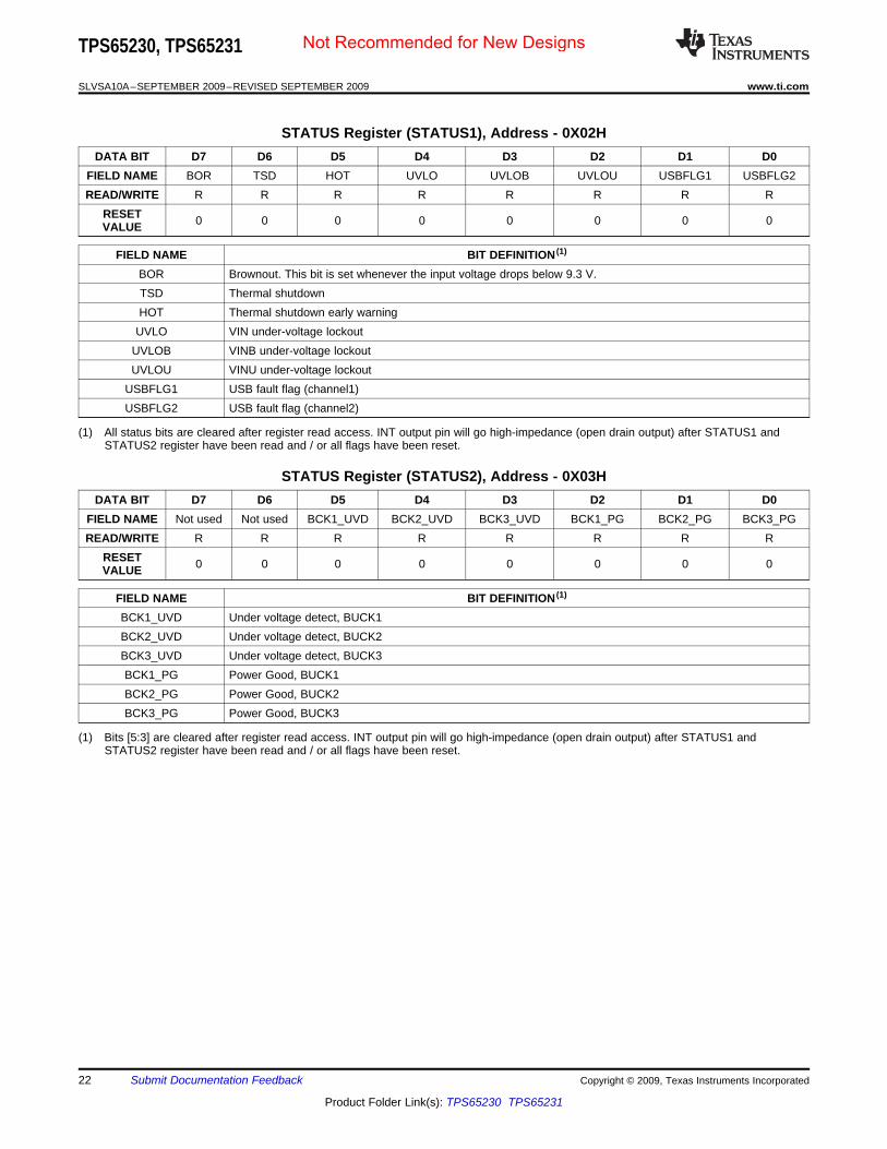
STATUS Register (STATUS1), Address - 0X02HDATA BIT D7 D6 D5 D4 D3 D2 D1 D0
FIELD NAME BOR TSD HOT UVLO UVLOB UVLOU USBFLG1 USBFLG2READ/WRITE R R R R R R R R
RESET 0 0 0 0 0 0 0 0VALUE
FIELD NAME BIT DEFINITION (1)
BOR Brownout. This bit is set whenever the input voltage drops below 9.3 V.TSD Thermal shutdownHOT Thermal shutdown early warning
UVLO VIN under-voltage lockoutUVLOB VINB under-voltage lockoutUVLOU VINU under-voltage lockout
USBFLG1 USB fault flag (channel1)USBFLG2 USB fault flag (channel2)
(1) All status bits are cleared after register read access. INT output pin will go high-impedance (open drain output) after STATUS1 andSTATUS2 register have been read and / or all flags have been reset.
STATUS Register (STATUS2), Address - 0X03HDATA BIT D7 D6 D5 D4 D3 D2 D1 D0
FIELD NAME Not used Not used BCK1_UVD BCK2_UVD BCK3_UVD BCK1_PG BCK2_PG BCK3_PGREAD/WRITE R R R R R R R R
RESET 0 0 0 0 0 0 0 0VALUE
FIELD NAME BIT DEFINITION (1)
BCK1_UVD Under voltage detect, BUCK1BCK2_UVD Under voltage detect, BUCK2BCK3_UVD Under voltage detect, BUCK3BCK1_PG Power Good, BUCK1BCK2_PG Power Good, BUCK2BCK3_PG Power Good, BUCK3
(1) Bits [5:3] are cleared after register read access. INT output pin will go high-impedance (open drain output) after STATUS1 andSTATUS2 register have been read and / or all flags have been reset.
22 Submit Documentation Feedback Copyright © 2009, Texas Instruments Incorporated
Product Folder Link(s): TPS65230 TPS65231
Not Recommended for New Designs

PACKAGE OPTION ADDENDUM
www.ti.com 15-Apr-2017
Addendum-Page 1
PACKAGING INFORMATION
Orderable Device Status(1)
Package Type PackageDrawing
Pins PackageQty
Eco Plan(2)
Lead/Ball Finish(6)
MSL Peak Temp(3)
Op Temp (°C) Device Marking(4/5)
Samples
TPS65230A2DCA NRND HTSSOP DCA 48 40 Green (RoHS& no Sb/Br)
CU NIPDAU Level-3-260C-168 HR 0 to 85 TPS65230A2
TPS65230A2DCAR NRND HTSSOP DCA 48 2000 Green (RoHS& no Sb/Br)
CU NIPDAU Level-3-260C-168 HR 0 to 85 TPS65230A2
TPS65231A2DCAR NRND HTSSOP DCA 48 2000 Green (RoHS& no Sb/Br)
CU NIPDAU Level-3-260C-168 HR 0 to 85 TPS65231A2
(1) The marketing status values are defined as follows:ACTIVE: Product device recommended for new designs.LIFEBUY: TI has announced that the device will be discontinued, and a lifetime-buy period is in effect.NRND: Not recommended for new designs. Device is in production to support existing customers, but TI does not recommend using this part in a new design.PREVIEW: Device has been announced but is not in production. Samples may or may not be available.OBSOLETE: TI has discontinued the production of the device.
(2) Eco Plan - The planned eco-friendly classification: Pb-Free (RoHS), Pb-Free (RoHS Exempt), or Green (RoHS & no Sb/Br) - please check http://www.ti.com/productcontent for the latest availabilityinformation and additional product content details.TBD: The Pb-Free/Green conversion plan has not been defined.Pb-Free (RoHS): TI's terms "Lead-Free" or "Pb-Free" mean semiconductor products that are compatible with the current RoHS requirements for all 6 substances, including the requirement thatlead not exceed 0.1% by weight in homogeneous materials. Where designed to be soldered at high temperatures, TI Pb-Free products are suitable for use in specified lead-free processes.Pb-Free (RoHS Exempt): This component has a RoHS exemption for either 1) lead-based flip-chip solder bumps used between the die and package, or 2) lead-based die adhesive used betweenthe die and leadframe. The component is otherwise considered Pb-Free (RoHS compatible) as defined above.Green (RoHS & no Sb/Br): TI defines "Green" to mean Pb-Free (RoHS compatible), and free of Bromine (Br) and Antimony (Sb) based flame retardants (Br or Sb do not exceed 0.1% by weightin homogeneous material)
(3) MSL, Peak Temp. - The Moisture Sensitivity Level rating according to the JEDEC industry standard classifications, and peak solder temperature.
(4) There may be additional marking, which relates to the logo, the lot trace code information, or the environmental category on the device.
(5) Multiple Device Markings will be inside parentheses. Only one Device Marking contained in parentheses and separated by a "~" will appear on a device. If a line is indented then it is a continuationof the previous line and the two combined represent the entire Device Marking for that device.
(6) Lead/Ball Finish - Orderable Devices may have multiple material finish options. Finish options are separated by a vertical ruled line. Lead/Ball Finish values may wrap to two lines if the finishvalue exceeds the maximum column width.
Important Information and Disclaimer:The information provided on this page represents TI's knowledge and belief as of the date that it is provided. TI bases its knowledge and belief on informationprovided by third parties, and makes no representation or warranty as to the accuracy of such information. Efforts are underway to better integrate information from third parties. TI has taken and

PACKAGE OPTION ADDENDUM
www.ti.com 15-Apr-2017
Addendum-Page 2
continues to take reasonable steps to provide representative and accurate information but may not have conducted destructive testing or chemical analysis on incoming materials and chemicals.TI and TI suppliers consider certain information to be proprietary, and thus CAS numbers and other limited information may not be available for release.
In no event shall TI's liability arising out of such information exceed the total purchase price of the TI part(s) at issue in this document sold by TI to Customer on an annual basis.

TAPE AND REEL INFORMATION
*All dimensions are nominal
Device PackageType
PackageDrawing
Pins SPQ ReelDiameter
(mm)
ReelWidth
W1 (mm)
A0(mm)
B0(mm)
K0(mm)
P1(mm)
W(mm)
Pin1Quadrant
TPS65230A2DCAR HTSSOP DCA 48 2000 330.0 24.4 8.6 13.0 1.8 12.0 24.0 Q1
TPS65231A2DCAR HTSSOP DCA 48 2000 330.0 24.4 8.6 13.0 1.8 12.0 24.0 Q1
PACKAGE MATERIALS INFORMATION
www.ti.com 14-Dec-2017
Pack Materials-Page 1

*All dimensions are nominal
Device Package Type Package Drawing Pins SPQ Length (mm) Width (mm) Height (mm)
TPS65230A2DCAR HTSSOP DCA 48 2000 367.0 367.0 45.0
TPS65231A2DCAR HTSSOP DCA 48 2000 367.0 367.0 45.0
PACKAGE MATERIALS INFORMATION
www.ti.com 14-Dec-2017
Pack Materials-Page 2

IMPORTANT NOTICE
Texas Instruments Incorporated (TI) reserves the right to make corrections, enhancements, improvements and other changes to itssemiconductor products and services per JESD46, latest issue, and to discontinue any product or service per JESD48, latest issue. Buyersshould obtain the latest relevant information before placing orders and should verify that such information is current and complete.TI’s published terms of sale for semiconductor products (http://www.ti.com/sc/docs/stdterms.htm) apply to the sale of packaged integratedcircuit products that TI has qualified and released to market. Additional terms may apply to the use or sale of other types of TI products andservices.Reproduction of significant portions of TI information in TI data sheets is permissible only if reproduction is without alteration and isaccompanied by all associated warranties, conditions, limitations, and notices. TI is not responsible or liable for such reproduceddocumentation. Information of third parties may be subject to additional restrictions. Resale of TI products or services with statementsdifferent from or beyond the parameters stated by TI for that product or service voids all express and any implied warranties for theassociated TI product or service and is an unfair and deceptive business practice. TI is not responsible or liable for any such statements.Buyers and others who are developing systems that incorporate TI products (collectively, “Designers”) understand and agree that Designersremain responsible for using their independent analysis, evaluation and judgment in designing their applications and that Designers havefull and exclusive responsibility to assure the safety of Designers' applications and compliance of their applications (and of all TI productsused in or for Designers’ applications) with all applicable regulations, laws and other applicable requirements. Designer represents that, withrespect to their applications, Designer has all the necessary expertise to create and implement safeguards that (1) anticipate dangerousconsequences of failures, (2) monitor failures and their consequences, and (3) lessen the likelihood of failures that might cause harm andtake appropriate actions. Designer agrees that prior to using or distributing any applications that include TI products, Designer willthoroughly test such applications and the functionality of such TI products as used in such applications.TI’s provision of technical, application or other design advice, quality characterization, reliability data or other services or information,including, but not limited to, reference designs and materials relating to evaluation modules, (collectively, “TI Resources”) are intended toassist designers who are developing applications that incorporate TI products; by downloading, accessing or using TI Resources in anyway, Designer (individually or, if Designer is acting on behalf of a company, Designer’s company) agrees to use any particular TI Resourcesolely for this purpose and subject to the terms of this Notice.TI’s provision of TI Resources does not expand or otherwise alter TI’s applicable published warranties or warranty disclaimers for TIproducts, and no additional obligations or liabilities arise from TI providing such TI Resources. TI reserves the right to make corrections,enhancements, improvements and other changes to its TI Resources. TI has not conducted any testing other than that specificallydescribed in the published documentation for a particular TI Resource.Designer is authorized to use, copy and modify any individual TI Resource only in connection with the development of applications thatinclude the TI product(s) identified in such TI Resource. NO OTHER LICENSE, EXPRESS OR IMPLIED, BY ESTOPPEL OR OTHERWISETO ANY OTHER TI INTELLECTUAL PROPERTY RIGHT, AND NO LICENSE TO ANY TECHNOLOGY OR INTELLECTUAL PROPERTYRIGHT OF TI OR ANY THIRD PARTY IS GRANTED HEREIN, including but not limited to any patent right, copyright, mask work right, orother intellectual property right relating to any combination, machine, or process in which TI products or services are used. Informationregarding or referencing third-party products or services does not constitute a license to use such products or services, or a warranty orendorsement thereof. Use of TI Resources may require a license from a third party under the patents or other intellectual property of thethird party, or a license from TI under the patents or other intellectual property of TI.TI RESOURCES ARE PROVIDED “AS IS” AND WITH ALL FAULTS. TI DISCLAIMS ALL OTHER WARRANTIES ORREPRESENTATIONS, EXPRESS OR IMPLIED, REGARDING RESOURCES OR USE THEREOF, INCLUDING BUT NOT LIMITED TOACCURACY OR COMPLETENESS, TITLE, ANY EPIDEMIC FAILURE WARRANTY AND ANY IMPLIED WARRANTIES OFMERCHANTABILITY, FITNESS FOR A PARTICULAR PURPOSE, AND NON-INFRINGEMENT OF ANY THIRD PARTY INTELLECTUALPROPERTY RIGHTS. TI SHALL NOT BE LIABLE FOR AND SHALL NOT DEFEND OR INDEMNIFY DESIGNER AGAINST ANY CLAIM,INCLUDING BUT NOT LIMITED TO ANY INFRINGEMENT CLAIM THAT RELATES TO OR IS BASED ON ANY COMBINATION OFPRODUCTS EVEN IF DESCRIBED IN TI RESOURCES OR OTHERWISE. IN NO EVENT SHALL TI BE LIABLE FOR ANY ACTUAL,DIRECT, SPECIAL, COLLATERAL, INDIRECT, PUNITIVE, INCIDENTAL, CONSEQUENTIAL OR EXEMPLARY DAMAGES INCONNECTION WITH OR ARISING OUT OF TI RESOURCES OR USE THEREOF, AND REGARDLESS OF WHETHER TI HAS BEENADVISED OF THE POSSIBILITY OF SUCH DAMAGES.Unless TI has explicitly designated an individual product as meeting the requirements of a particular industry standard (e.g., ISO/TS 16949and ISO 26262), TI is not responsible for any failure to meet such industry standard requirements.Where TI specifically promotes products as facilitating functional safety or as compliant with industry functional safety standards, suchproducts are intended to help enable customers to design and create their own applications that meet applicable functional safety standardsand requirements. Using products in an application does not by itself establish any safety features in the application. Designers mustensure compliance with safety-related requirements and standards applicable to their applications. Designer may not use any TI products inlife-critical medical equipment unless authorized officers of the parties have executed a special contract specifically governing such use.Life-critical medical equipment is medical equipment where failure of such equipment would cause serious bodily injury or death (e.g., lifesupport, pacemakers, defibrillators, heart pumps, neurostimulators, and implantables). Such equipment includes, without limitation, allmedical devices identified by the U.S. Food and Drug Administration as Class III devices and equivalent classifications outside the U.S.TI may expressly designate certain products as completing a particular qualification (e.g., Q100, Military Grade, or Enhanced Product).Designers agree that it has the necessary expertise to select the product with the appropriate qualification designation for their applicationsand that proper product selection is at Designers’ own risk. Designers are solely responsible for compliance with all legal and regulatoryrequirements in connection with such selection.Designer will fully indemnify TI and its representatives against any damages, costs, losses, and/or liabilities arising out of Designer’s non-compliance with the terms and provisions of this Notice.
Mailing Address: Texas Instruments, Post Office Box 655303, Dallas, Texas 75265Copyright © 2017, Texas Instruments Incorporated


![Secure JTAG implementation using Schnorr Protocol · via the JTAG interface into FPGAs [7]. The firmware update of set-top boxes used in pay-TV The firmware update of set-top boxes](https://static.fdocuments.net/doc/165x107/5b5d5cfc7f8b9a68368ead46/secure-jtag-implementation-using-schnorr-protocol-via-the-jtag-interface-into.jpg)