PON Triplexer and SFP Controller - Maxim Integrated · PON Triplexer and SFP Controller _____ 5....
92
General Description The DS1875 controls and monitors all functions for burst- mode transmitters, APD receivers, and video receivers. It also includes a power-supply controller for APD bias generation, and provides all SFF-8472 diagnostic and monitoring functionality. The combined solution of the DS1875 and the MAX3643 laser driver provides APC loop, modulation current control, and eye safety func- tionality. Ten ADC channels monitor V CC , temperature (both internal signals), and eight external monitor inputs (MON1–MON8) that can be used to meet transmitter, digital receiver, video receiver, and APD receiver-signal monitoring requirements. Four total DAC outputs are available. A PWM controller with feedback and compen- sation pins can be used to generate the bias for an APD or as a step-down converter. Five I/O pins allow addi- tional monitoring and configuration. Applications BPON, GPON, or EPON Optical Triplexers SFF, SFP, and SFP+ Transceiver Modules APD Controller Features ♦ Meets All PON Burst-Timing Requirements for Burst-Mode Operation ♦ Laser Bias Controlled by APC Loop and Temperature Lookup Table (LUT) ♦ Laser Modulation Controlled by Temperature LUT ♦ Six Total DACs: Four External, Two Internal ♦ Two 8-Bit DACs, One of Which is Optionally Controlled by MON4 Voltage ♦ Internal 8-Bit DAC Controlled by a Temperature- Indexed LUT ♦ PWM Controller ♦ Boost or Buck Mode ♦ Boost Mode: Uses Optional External Components, Up to 90V Bias Generation ♦ 131kHz, 262kHz, 525kHz, or 1050kHz Selectable- Switching Frequency ♦ APD Overcurrent Protection Using Optional Fast Shutdown ♦ 10 Analog Monitor Channels: Temperature, V CC , Eight Monitors ♦ Internal, Factory-Calibrated Temperature Sensor ♦ RSSI with 29dB Electrical Dynamic ♦ Five I/O Pins for Additional Control and Monitoring Functions, Four of Which are Either Digital I/O or Analog Monitors ♦ Comprehensive Fault-Measurement System with Maskable Laser Shutdown Capability ♦ Two-Level Password Access to Protect Calibration Data ♦ 120 Bytes of Password-1 Protected Memory ♦ 128 Bytes of Password-2 Protected Memory in Main Device Address ♦ 256 Additional Bytes Located at A0h Slave Address ♦ I 2 C-Compatible Interface for Calibration and Monitoring ♦ 2.85V to 3.9V Operating Voltage Range ♦ -40°C to +95°C Operating Temperature Range ♦ 38-Pin TQFN (5mm x 7mm) Package DS1875 ________________________________________________________________ Maxim Integrated Products 1 TOP VIEW TQFN (5mm × 7mm × 0.8mm) 13 14 15 16 17 18 19 MON5/D0 MON6/D1 MON7/D2 MON8/D3 MON1 MON2 MON4 38 37 36 35 34 33 32 1 2 3 4 5 6 7 8 9 10 11 12 N.C. N.C. N.C. V CC SW GND GND LOSI N.C. GND V CC TX-D N.C. FETG N.C. TX-F SCL SDA BEN 31 30 29 28 27 26 25 24 23 22 21 20 N.C. MON3N MON3P DAC1 GND M4DAC FB BIAS MOD COMP BMD V CC + *EP *EXPOSED PAD. DS1875 Pin Configuration Ordering Information Rev 1; 10/08 For pricing, delivery, and ordering information, please contact Maxim Direct at 1-888-629-4642, or visit Maxim’s website at www.maxim-ic.com. +Denotes a lead-free/RoHS-compliant package. T&R = Tape and reel. *EP = Exposed pad. PART TEMP RANGE PIN-PACKAGE DS1875T+ -40°C to +95°C 38 TQFN-EP* DS1875T+T&R -40°C to +95°C 38 TQFN-EP* PON Triplexer and SFP Controller
Transcript of PON Triplexer and SFP Controller - Maxim Integrated · PON Triplexer and SFP Controller _____ 5....
General DescriptionThe DS1875 controls and monitors all functions for burst-mode transmitters, APD receivers, and video receivers.It also includes a power-supply controller for APD biasgeneration, and provides all SFF-8472 diagnostic andmonitoring functionality. The combined solution of theDS1875 and the MAX3643 laser driver provides APCloop, modulation current control, and eye safety func-tionality. Ten ADC channels monitor VCC, temperature(both internal signals), and eight external monitor inputs(MON1–MON8) that can be used to meet transmitter,digital receiver, video receiver, and APD receiver-signalmonitoring requirements. Four total DAC outputs areavailable. A PWM controller with feedback and compen-sation pins can be used to generate the bias for an APDor as a step-down converter. Five I/O pins allow addi-tional monitoring and configuration.
ApplicationsBPON, GPON, or EPON Optical Triplexers
SFF, SFP, and SFP+ Transceiver Modules
APD Controller
Features♦ Meets All PON Burst-Timing Requirements for
Burst-Mode Operation
♦ Laser Bias Controlled by APC Loop andTemperature Lookup Table (LUT)
♦ Laser Modulation Controlled by Temperature LUT
♦ Six Total DACs: Four External, Two Internal
♦ Two 8-Bit DACs, One of Which is OptionallyControlled by MON4 Voltage
♦ Internal 8-Bit DAC Controlled by a Temperature-Indexed LUT
♦ PWM Controller
♦ Boost or Buck Mode
♦ Boost Mode: Uses Optional ExternalComponents, Up to 90V Bias Generation
♦ 131kHz, 262kHz, 525kHz, or 1050kHz Selectable-Switching Frequency
♦ APD Overcurrent Protection Using Optional FastShutdown
♦ 10 Analog Monitor Channels: Temperature, VCC,Eight Monitors
♦ Internal, Factory-Calibrated Temperature Sensor
♦ RSSI with 29dB Electrical Dynamic
♦ Five I/O Pins for Additional Control andMonitoring Functions, Four of Which are EitherDigital I/O or Analog Monitors
♦ Comprehensive Fault-Measurement System withMaskable Laser Shutdown Capability
♦ Two-Level Password Access to ProtectCalibration Data
♦ 120 Bytes of Password-1 Protected Memory
♦ 128 Bytes of Password-2 Protected Memory inMain Device Address
♦ 256 Additional Bytes Located at A0h SlaveAddress
♦ I2C-Compatible Interface for Calibration andMonitoring
♦ 2.85V to 3.9V Operating Voltage Range
♦ -40°C to +95°C Operating Temperature Range
♦ 38-Pin TQFN (5mm x 7mm) Package
DS
18
75
________________________________________________________________ Maxim Integrated Products 1
TOP VIEW
TQFN(5mm × 7mm × 0.8mm)
13
14
15
16
17
18
19
MON5/D0
MON6/D1
MON7/D2
MON8/D3
MON1
MON2
MON4
38
37
36
35
34
33
32
1 2 3 4 5 6 7 8 9 10 11 12
N.C.
N.C.
N.C.
VCC
SW
GND
GND
LOSI
N.C.
GND
V CC
TX-D
N.C.
FETGN.C.
TX-F
SCL
SDA
BEN
31 30 29 28 27 26 25 24 23 22 21 20
N.C.
MON
3N
MON
3P
DAC1
GND
M4D
AC
FBBIAS
MOD
COM
P
BMD
V CC
+ *EP
*EXPOSED PAD.
DS1875
Pin Configuration
Ordering Information
Rev 1; 10/08
For pricing, delivery, and ordering information, please contact Maxim Direct at 1-888-629-4642,or visit Maxim’s website at www.maxim-ic.com.
+Denotes a lead-free/RoHS-compliant package.T&R = Tape and reel.*EP = Exposed pad.
PART TEMP RANGE PIN-PACKAGE
DS1875T+ -40°C to +95°C 38 TQFN-EP*
DS1875T+T&R -40°C to +95°C 38 TQFN-EP*
PON Triplexer and SFP Controller
DS
18
75
2 _______________________________________________________________________________________
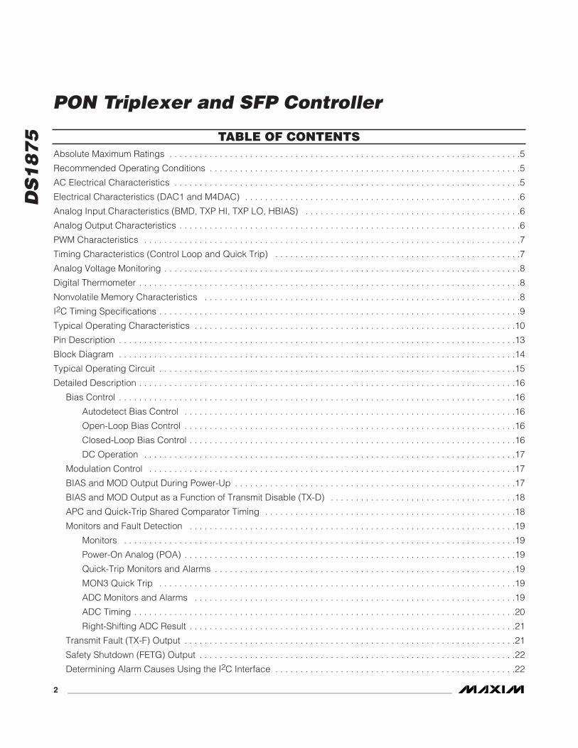
Absolute Maximum Ratings . . . . . . . . . . . . . . . . . . . . . . . . . . . . . . . . . . . . . . . . . . . . . . . . . . . . . . . . . . . . . . . . . . . . . .5
Recommended Operating Conditions . . . . . . . . . . . . . . . . . . . . . . . . . . . . . . . . . . . . . . . . . . . . . . . . . . . . . . . . . . . . . .5
AC Electrical Characteristics . . . . . . . . . . . . . . . . . . . . . . . . . . . . . . . . . . . . . . . . . . . . . . . . . . . . . . . . . . . . . . . . . . . . .5
Electrical Characteristics (DAC1 and M4DAC) . . . . . . . . . . . . . . . . . . . . . . . . . . . . . . . . . . . . . . . . . . . . . . . . . . . . . . .6
Analog Input Characteristics (BMD, TXP HI, TXP LO, HBIAS) . . . . . . . . . . . . . . . . . . . . . . . . . . . . . . . . . . . . . . . . . . .6
Analog Output Characteristics . . . . . . . . . . . . . . . . . . . . . . . . . . . . . . . . . . . . . . . . . . . . . . . . . . . . . . . . . . . . . . . . . . . .6
PWM Characteristics . . . . . . . . . . . . . . . . . . . . . . . . . . . . . . . . . . . . . . . . . . . . . . . . . . . . . . . . . . . . . . . . . . . . . . . . . . .7
Timing Characteristics (Control Loop and Quick Trip) . . . . . . . . . . . . . . . . . . . . . . . . . . . . . . . . . . . . . . . . . . . . . . . . .7
Analog Voltage Monitoring . . . . . . . . . . . . . . . . . . . . . . . . . . . . . . . . . . . . . . . . . . . . . . . . . . . . . . . . . . . . . . . . . . . . . . .8
Digital Thermometer . . . . . . . . . . . . . . . . . . . . . . . . . . . . . . . . . . . . . . . . . . . . . . . . . . . . . . . . . . . . . . . . . . . . . . . . . . . .8
Nonvolatile Memory Characteristics . . . . . . . . . . . . . . . . . . . . . . . . . . . . . . . . . . . . . . . . . . . . . . . . . . . . . . . . . . . . . . .8
I2C Timing Specifications . . . . . . . . . . . . . . . . . . . . . . . . . . . . . . . . . . . . . . . . . . . . . . . . . . . . . . . . . . . . . . . . . . . . . . . .9
Typical Operating Characteristics . . . . . . . . . . . . . . . . . . . . . . . . . . . . . . . . . . . . . . . . . . . . . . . . . . . . . . . . . . . . . . . .10
Pin Description . . . . . . . . . . . . . . . . . . . . . . . . . . . . . . . . . . . . . . . . . . . . . . . . . . . . . . . . . . . . . . . . . . . . . . . . . . . . . . .13
Block Diagram . . . . . . . . . . . . . . . . . . . . . . . . . . . . . . . . . . . . . . . . . . . . . . . . . . . . . . . . . . . . . . . . . . . . . . . . . . . . . . .14
Typical Operating Circuit . . . . . . . . . . . . . . . . . . . . . . . . . . . . . . . . . . . . . . . . . . . . . . . . . . . . . . . . . . . . . . . . . . . . . . .15
Detailed Description . . . . . . . . . . . . . . . . . . . . . . . . . . . . . . . . . . . . . . . . . . . . . . . . . . . . . . . . . . . . . . . . . . . . . . . . . . .16
Bias Control . . . . . . . . . . . . . . . . . . . . . . . . . . . . . . . . . . . . . . . . . . . . . . . . . . . . . . . . . . . . . . . . . . . . . . . . . . . . . . .16
Autodetect Bias Control . . . . . . . . . . . . . . . . . . . . . . . . . . . . . . . . . . . . . . . . . . . . . . . . . . . . . . . . . . . . . . . . . .16
Open-Loop Bias Control . . . . . . . . . . . . . . . . . . . . . . . . . . . . . . . . . . . . . . . . . . . . . . . . . . . . . . . . . . . . . . . . . .16
Closed-Loop Bias Control . . . . . . . . . . . . . . . . . . . . . . . . . . . . . . . . . . . . . . . . . . . . . . . . . . . . . . . . . . . . . . . . .16
DC Operation . . . . . . . . . . . . . . . . . . . . . . . . . . . . . . . . . . . . . . . . . . . . . . . . . . . . . . . . . . . . . . . . . . . . . . . . . .17
Modulation Control . . . . . . . . . . . . . . . . . . . . . . . . . . . . . . . . . . . . . . . . . . . . . . . . . . . . . . . . . . . . . . . . . . . . . . . . .17
BIAS and MOD Output During Power-Up . . . . . . . . . . . . . . . . . . . . . . . . . . . . . . . . . . . . . . . . . . . . . . . . . . . . . . . .17
BIAS and MOD Output as a Function of Transmit Disable (TX-D) . . . . . . . . . . . . . . . . . . . . . . . . . . . . . . . . . . . . .18
APC and Quick-Trip Shared Comparator Timing . . . . . . . . . . . . . . . . . . . . . . . . . . . . . . . . . . . . . . . . . . . . . . . . . .18
Monitors and Fault Detection . . . . . . . . . . . . . . . . . . . . . . . . . . . . . . . . . . . . . . . . . . . . . . . . . . . . . . . . . . . . . . . . .19
Monitors . . . . . . . . . . . . . . . . . . . . . . . . . . . . . . . . . . . . . . . . . . . . . . . . . . . . . . . . . . . . . . . . . . . . . . . . . . . . . .19
Power-On Analog (POA) . . . . . . . . . . . . . . . . . . . . . . . . . . . . . . . . . . . . . . . . . . . . . . . . . . . . . . . . . . . . . . . . . .19
Quick-Trip Monitors and Alarms . . . . . . . . . . . . . . . . . . . . . . . . . . . . . . . . . . . . . . . . . . . . . . . . . . . . . . . . . . . .19
MON3 Quick Trip . . . . . . . . . . . . . . . . . . . . . . . . . . . . . . . . . . . . . . . . . . . . . . . . . . . . . . . . . . . . . . . . . . . . . . .19
ADC Monitors and Alarms . . . . . . . . . . . . . . . . . . . . . . . . . . . . . . . . . . . . . . . . . . . . . . . . . . . . . . . . . . . . . . . .19
ADC Timing . . . . . . . . . . . . . . . . . . . . . . . . . . . . . . . . . . . . . . . . . . . . . . . . . . . . . . . . . . . . . . . . . . . . . . . . . . . .20
Right-Shifting ADC Result . . . . . . . . . . . . . . . . . . . . . . . . . . . . . . . . . . . . . . . . . . . . . . . . . . . . . . . . . . . . . . . . .21
Transmit Fault (TX-F) Output . . . . . . . . . . . . . . . . . . . . . . . . . . . . . . . . . . . . . . . . . . . . . . . . . . . . . . . . . . . . . . . . . .21
Safety Shutdown (FETG) Output . . . . . . . . . . . . . . . . . . . . . . . . . . . . . . . . . . . . . . . . . . . . . . . . . . . . . . . . . . . . . . .22
Determining Alarm Causes Using the I2C Interface . . . . . . . . . . . . . . . . . . . . . . . . . . . . . . . . . . . . . . . . . . . . . . . .22
TABLE OF CONTENTS
PON Triplexer and SFP Controller

DS
18
75
_______________________________________________________________________________________ 3
Die Identification . . . . . . . . . . . . . . . . . . . . . . . . . . . . . . . . . . . . . . . . . . . . . . . . . . . . . . . . . . . . . . . . . . . . . . . . . . .23
Low-Voltage Operation . . . . . . . . . . . . . . . . . . . . . . . . . . . . . . . . . . . . . . . . . . . . . . . . . . . . . . . . . . . . . . . . . . . . . .23
Enhanced RSSI Monitoring (Dual Range Functionality) . . . . . . . . . . . . . . . . . . . . . . . . . . . . . . . . . . . . . . . . . . . . .23
PWM Controller . . . . . . . . . . . . . . . . . . . . . . . . . . . . . . . . . . . . . . . . . . . . . . . . . . . . . . . . . . . . . . . . . . . . . . . . . . . .25
Inductor Selection . . . . . . . . . . . . . . . . . . . . . . . . . . . . . . . . . . . . . . . . . . . . . . . . . . . . . . . . . . . . . . . . . . . . . . .26
Stability and Compensation Component Selection . . . . . . . . . . . . . . . . . . . . . . . . . . . . . . . . . . . . . . . . . . . . .27
DAC1 Output . . . . . . . . . . . . . . . . . . . . . . . . . . . . . . . . . . . . . . . . . . . . . . . . . . . . . . . . . . . . . . . . . . . . . . . . . . . . . .27
M4DAC Output . . . . . . . . . . . . . . . . . . . . . . . . . . . . . . . . . . . . . . . . . . . . . . . . . . . . . . . . . . . . . . . . . . . . . . . . . . . .27
Digital I/O Pins . . . . . . . . . . . . . . . . . . . . . . . . . . . . . . . . . . . . . . . . . . . . . . . . . . . . . . . . . . . . . . . . . . . . . . . . . . . . .27
I2C Communication . . . . . . . . . . . . . . . . . . . . . . . . . . . . . . . . . . . . . . . . . . . . . . . . . . . . . . . . . . . . . . . . . . . . . . . . . . .29
I2C Definitions . . . . . . . . . . . . . . . . . . . . . . . . . . . . . . . . . . . . . . . . . . . . . . . . . . . . . . . . . . . . . . . . . . . . . . . . . . . . .29
I2C Protocol . . . . . . . . . . . . . . . . . . . . . . . . . . . . . . . . . . . . . . . . . . . . . . . . . . . . . . . . . . . . . . . . . . . . . . . . . . . . . . .30
Memory Map . . . . . . . . . . . . . . . . . . . . . . . . . . . . . . . . . . . . . . . . . . . . . . . . . . . . . . . . . . . . . . . . . . . . . . . . . . . . . . . .31
Memory Organization . . . . . . . . . . . . . . . . . . . . . . . . . . . . . . . . . . . . . . . . . . . . . . . . . . . . . . . . . . . . . . . . . . . . . . .31
Shadowed EEPROM . . . . . . . . . . . . . . . . . . . . . . . . . . . . . . . . . . . . . . . . . . . . . . . . . . . . . . . . . . . . . . . . . . . . . . . .32
Register Descriptions . . . . . . . . . . . . . . . . . . . . . . . . . . . . . . . . . . . . . . . . . . . . . . . . . . . . . . . . . . . . . . . . . . . . . . . . . .33
Lower Memory Register Map . . . . . . . . . . . . . . . . . . . . . . . . . . . . . . . . . . . . . . . . . . . . . . . . . . . . . . . . . . . . . . . . .33
Table 00h Register Map . . . . . . . . . . . . . . . . . . . . . . . . . . . . . . . . . . . . . . . . . . . . . . . . . . . . . . . . . . . . . . . . . . . . .34
Table 01h Register Map . . . . . . . . . . . . . . . . . . . . . . . . . . . . . . . . . . . . . . . . . . . . . . . . . . . . . . . . . . . . . . . . . . . . .35
Table 02h Register Map . . . . . . . . . . . . . . . . . . . . . . . . . . . . . . . . . . . . . . . . . . . . . . . . . . . . . . . . . . . . . . . . . . . . .36
Table 03h Register Map . . . . . . . . . . . . . . . . . . . . . . . . . . . . . . . . . . . . . . . . . . . . . . . . . . . . . . . . . . . . . . . . . . . . .37
Table 04h Register Map . . . . . . . . . . . . . . . . . . . . . . . . . . . . . . . . . . . . . . . . . . . . . . . . . . . . . . . . . . . . . . . . . . . . .38
Table 05h Register Map . . . . . . . . . . . . . . . . . . . . . . . . . . . . . . . . . . . . . . . . . . . . . . . . . . . . . . . . . . . . . . . . . . . . .38
Table 06h Register Map . . . . . . . . . . . . . . . . . . . . . . . . . . . . . . . . . . . . . . . . . . . . . . . . . . . . . . . . . . . . . . . . . . . . .39
Table 07h Register Map . . . . . . . . . . . . . . . . . . . . . . . . . . . . . . . . . . . . . . . . . . . . . . . . . . . . . . . . . . . . . . . . . . . . .39
Table 08h Register Map . . . . . . . . . . . . . . . . . . . . . . . . . . . . . . . . . . . . . . . . . . . . . . . . . . . . . . . . . . . . . . . . . . . . .40
Auxiliary A0h Memory Register Map . . . . . . . . . . . . . . . . . . . . . . . . . . . . . . . . . . . . . . . . . . . . . . . . . . . . . . . . . . . .41
Lower Memory Register Descriptions . . . . . . . . . . . . . . . . . . . . . . . . . . . . . . . . . . . . . . . . . . . . . . . . . . . . . . . . . . .42
Table 00h Register Descriptions . . . . . . . . . . . . . . . . . . . . . . . . . . . . . . . . . . . . . . . . . . . . . . . . . . . . . . . . . . . . . . .57
Table 01h Register Descriptions . . . . . . . . . . . . . . . . . . . . . . . . . . . . . . . . . . . . . . . . . . . . . . . . . . . . . . . . . . . . . . .57
Table 02h Register Descriptions . . . . . . . . . . . . . . . . . . . . . . . . . . . . . . . . . . . . . . . . . . . . . . . . . . . . . . . . . . . . . . .61
Table 03h Register Descriptions . . . . . . . . . . . . . . . . . . . . . . . . . . . . . . . . . . . . . . . . . . . . . . . . . . . . . . . . . . . . . . .87
Table 04h Register Descriptions . . . . . . . . . . . . . . . . . . . . . . . . . . . . . . . . . . . . . . . . . . . . . . . . . . . . . . . . . . . . . . .87
Table 05h Register Descriptions . . . . . . . . . . . . . . . . . . . . . . . . . . . . . . . . . . . . . . . . . . . . . . . . . . . . . . . . . . . . . . .88
Table 06h Register Descriptions . . . . . . . . . . . . . . . . . . . . . . . . . . . . . . . . . . . . . . . . . . . . . . . . . . . . . . . . . . . . . . .89
Table 07h Register Descriptions . . . . . . . . . . . . . . . . . . . . . . . . . . . . . . . . . . . . . . . . . . . . . . . . . . . . . . . . . . . . . . .90
Table 08h Register Descriptions . . . . . . . . . . . . . . . . . . . . . . . . . . . . . . . . . . . . . . . . . . . . . . . . . . . . . . . . . . . . . . .91
TABLE OF CONTENTS (continued)
PON Triplexer and SFP Controller

DS
18
75
PON Triplexer and SFP Controller
4 _______________________________________________________________________________________
Auxiliary Memory A0h Register Descriptions . . . . . . . . . . . . . . . . . . . . . . . . . . . . . . . . . . . . . . . . . . . . . . . . . . . . .91
Package Information . . . . . . . . . . . . . . . . . . . . . . . . . . . . . . . . . . . . . . . . . . . . . . . . . . . . . . . . . . . . . . . . . . . . . . . . . .91
TABLE OF CONTENTS (continued)
Figure 1. Power-Up Timing (BEN is a Long Burst) . . . . . . . . . . . . . . . . . . . . . . . . . . . . . . . . . . . . . . . . . . . . . . . . . . . .17
Figure 2. TX-D Timing . . . . . . . . . . . . . . . . . . . . . . . . . . . . . . . . . . . . . . . . . . . . . . . . . . . . . . . . . . . . . . . . . . . . . . . . .18
Figure 3. APC Loop and Quick-Trip Sample Timing . . . . . . . . . . . . . . . . . . . . . . . . . . . . . . . . . . . . . . . . . . . . . . . . . .18
Figure 4. M3QT Timing . . . . . . . . . . . . . . . . . . . . . . . . . . . . . . . . . . . . . . . . . . . . . . . . . . . . . . . . . . . . . . . . . . . . . . . . .20
Figure 5. ADC Timing with EN5TO8B = 0 . . . . . . . . . . . . . . . . . . . . . . . . . . . . . . . . . . . . . . . . . . . . . . . . . . . . . . . . . .20
Figure 6. ADC Timing with EN5TO8B = 1 . . . . . . . . . . . . . . . . . . . . . . . . . . . . . . . . . . . . . . . . . . . . . . . . . . . . . . . . . .20
Figure 7. TX-F Timing . . . . . . . . . . . . . . . . . . . . . . . . . . . . . . . . . . . . . . . . . . . . . . . . . . . . . . . . . . . . . . . . . . . . . . . . . .21
Figure 8. FETG/Output Disable Timing (Fault Condition Detected) . . . . . . . . . . . . . . . . . . . . . . . . . . . . . . . . . . . . . . .22
Figure 9. SEE Timing . . . . . . . . . . . . . . . . . . . . . . . . . . . . . . . . . . . . . . . . . . . . . . . . . . . . . . . . . . . . . . . . . . . . . . . . . .23
Figure 10. RSSI Flowchart . . . . . . . . . . . . . . . . . . . . . . . . . . . . . . . . . . . . . . . . . . . . . . . . . . . . . . . . . . . . . . . . . . . . . .24
Figure 11. PWM Controller Diagram . . . . . . . . . . . . . . . . . . . . . . . . . . . . . . . . . . . . . . . . . . . . . . . . . . . . . . . . . . . . . .25
Figure 12. PWM Controller Typical APD Bias Circuit . . . . . . . . . . . . . . . . . . . . . . . . . . . . . . . . . . . . . . . . . . . . . . . . . .28
Figure 13. PWM Controller Voltage Output Configuration . . . . . . . . . . . . . . . . . . . . . . . . . . . . . . . . . . . . . . . . . . . . . .28
Figure 14. PWM Controller Current-Sink Output Configuration . . . . . . . . . . . . . . . . . . . . . . . . . . . . . . . . . . . . . . . . . .28
Figure 15. I2C Timing Diagram . . . . . . . . . . . . . . . . . . . . . . . . . . . . . . . . . . . . . . . . . . . . . . . . . . . . . . . . . . . . . . . . . .29
Figure 16. Memory Map . . . . . . . . . . . . . . . . . . . . . . . . . . . . . . . . . . . . . . . . . . . . . . . . . . . . . . . . . . . . . . . . . . . . . . . .32
Table 1. DS1875 Acronyms . . . . . . . . . . . . . . . . . . . . . . . . . . . . . . . . . . . . . . . . . . . . . . . . . . . . . . . . . . . . . . . . . . . . .16
Table 2. Update Rate Timing . . . . . . . . . . . . . . . . . . . . . . . . . . . . . . . . . . . . . . . . . . . . . . . . . . . . . . . . . . . . . . . . . . . .18
Table 3. ADC Default Monitor Ranges . . . . . . . . . . . . . . . . . . . . . . . . . . . . . . . . . . . . . . . . . . . . . . . . . . . . . . . . . . . . .20
Table 4. TX-F as a Function of TX-D and Alarm Sources . . . . . . . . . . . . . . . . . . . . . . . . . . . . . . . . . . . . . . . . . . . . . . .21
Table 5. FETG, MOD, and BIAS Outputs as a Function of TX-D and Alarm Sources . . . . . . . . . . . . . . . . . . . . . . . . .22
Table 6. MON3 Configuration Registers . . . . . . . . . . . . . . . . . . . . . . . . . . . . . . . . . . . . . . . . . . . . . . . . . . . . . . . . . . .24
Table 7. MON3 Hysteresis Threshold Values . . . . . . . . . . . . . . . . . . . . . . . . . . . . . . . . . . . . . . . . . . . . . . . . . . . . . . .25
LIST OF FIGURES
LIST OF TABLES
DS
18
75
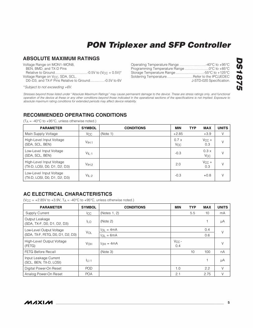
Stresses beyond those listed under “Absolute Maximum Ratings” may cause permanent damage to the device. These are stress ratings only, and functionaloperation of the device at these or any other conditions beyond those indicated in the operational sections of the specifications is not implied. Exposure toabsolute maximum rating conditions for extended periods may affect device reliability.
Voltage Range on MON1–MON8,BEN, BMD, and TX-D PinsRelative to Ground .................................-0.5V to (VCC + 0.5V)*
Voltage Range on VCC, SDA, SCL, D0–D3, and TX-F Pins Relative to Ground...............-0.5V to 6V
Operating Temperature Range ...........................-40°C to +95°C Programming Temperature Range .........................0°C to +85°CStorage Temperature Range .............................-55°C to +125°CSoldering Temperature...........................Refer to the IPC/JEDEC
J-STD-020 Specification.
PARAMETER SYMBOL CONDITIONS MIN TYP MAX UNITS
Main Supply Voltage VCC (Note 1) +2.85 +3.9 V
High-Level Input Voltage (SDA, SCL, BEN)
VIH:10.7 x VCC
VCC +0.3
V
Low-Level Input Voltage (SDA, SCL, BEN)
VIL:1 -0.3 0.3 x VCC
V
High-Level Input Voltage (TX-D, LOSI, D0, D1, D2, D3)
VIH:2 2.0 VCC +
0.3 V
Low-Level Input Voltage (TX-D, LOSI, D0, D1, D2, D3)
VIL:2 -0.3 +0.8 V
AC ELECTRICAL CHARACTERISTICS(VCC = +2.85V to +3.9V, TA = -40°C to +95°C, unless otherwise noted.)
PARAMETER SYMBOL CONDITIONS MIN TYP MAX UNITS
Supply Current ICC (Notes 1, 2) 5.5 10 mA
Output Leakage (SDA, TX-F, D0, D1, D2, D3)
ILO (Note 2) 1 μA
IOL = 4mA 0.4 Low-Level Output Voltage (SDA, TX-F, FETG, D0, D1, D2, D3)
VOLIOL = 6mA 0.6
V
High-Level Output Voltage (FETG)
VOH IOH = 4mA VCC -0.4
V
FETG Before Recall (Note 3) 10 100 nA
Input Leakage Current (SCL, BEN, TX-D, LOSI)
ILI:1 1 μA
Digital Power-On Reset POD 1.0 2.2 V
Analog Power-On Reset POA 2.1 2.75 V
*Subject to not exceeding +6V.
RECOMMENDED OPERATING CONDITIONS(TA = -40°C to +95°C, unless otherwise noted.)
ABSOLUTE MAXIMUM RATINGS
PON Triplexer and SFP Controller
_______________________________________________________________________________________ 5

DS
18
75
PON Triplexer and SFP Controller
6 _______________________________________________________________________________________
PARAMETER SYMBOL CONDITIONS MIN TYP MAX UNITS
DAC Output Range 2.5 V
DAC Output Resolution 8 Bits
DAC Output Integral Nonlinearity -1 +1 LSB
DAC Output Differential Nonlinearity
-1 +1 LSB
DAC Error TA = +25°C -1.25 +1.25 %FS
DAC Temperature Drift -2 +2 %FS
DAC Offset -12 +12 mV
Maximum Load -500 +500 μA
Maximum Load Capacitance 250 pF
PARAMETER SYMBOL CONDITIONS MIN TYP MAX UNITS
BMD, TXP HI, TXP LO Full-Scale Voltage
VAPC (Note 4) 2.5 V
HBIAS Full-Scale Voltage (Note 5) 1.25 V
BMD Input Resistance 35 50 65 k
Resolution 8 Bits
Error TA = +25°C (Note 6) ±2 %FS
Integral Nonlinearity -1 +1 LSB
Differential Nonlinearity -1 +1 LSB
Temperature Drift -2.5 +2.5 %FS
ANALOG OUTPUT CHARACTERISTICS(VCC = +2.85V to +3.9V, TA = -40°C to +95°C, unless otherwise noted.)
PARAMETER SYMBOL CONDITIONS MIN TYP MAX UNITS
BIAS Current IBIAS (Note 1) 1.2 mA
IBIAS Shutdown Current IBIAS:OFF 10 100 nA
Voltage at IBIAS 0.7 1.2 1.4 V
MOD Full-Scale Voltage VMOD (Note 5) 1.25 V
MOD Output Impedance (Note 7) 3 k
VMOD Error TA = +25°C (Note 8) -1.25 +1.25 %FS
VMOD Integral Nonlinearity -1 +1 LSB
VMOD Differential Nonlinearity -1 +1 LSB
VMOD Temperature Drift -2 +2 %FS
ANALOG INPUT CHARACTERISTICS (BMD, TXP HI, TXP LO, HBIAS)(VCC = +2.85V to +3.9V, TA = -40°C to +95°C, unless otherwise noted.)
ELECTRICAL CHARACTERISTICS (DAC1 AND M4DAC)(VCC = +2.85V to +3.9V, TA = -40°C to +95°C, unless otherwise noted.)

DS
18
75
PARAMETER SYMBOL CONDITIONS MIN TYP MAX UNITS
PWM-DAC Full-Scale Voltage VPWM-DAC 1.25 V
PWM-DAC Resolution 8 Bits
VPWM-DAC Full-Scale Voltage Error
TA = +25°C 1.25 %
VPWM-DAC Integral Nonlinearity -1 1 LSB
VPWM-DAC Differential Nonlinearity
-1 1 LSB
VPWM-DAC Temperature Drift -2 +2 %FS
SW Output Impedance 20
SW Frequency Error fSWER (Note 9) -5 +7 %
SW Duty Cycle DMAX 89 90 91 %
Error-Amplifier Source Current -10 μA
Error-Amplifier Sink Current +10 μA
COMP High-Voltage Clamp 2.1 V
COMP Low-Voltage Clamp 0.8 V
Error-Amplifier Transconductance
GM 425 μS
Error-Amplifier Output Impedance
REA 260 M
FB Pin Capacitance 5 pF
PARAMETER SYMBOL CONDITIONS MIN TYP MAX UNITS
First BMD Sample Following BEN tFIRST (Note 10)
Remaining Updates During BEN tUPDATE (Note 10)
BEN High Time tBEN:HIGH 400 ns
BEN Low Time tBEN:LOW 96 ns
Output-Enable Time Following POA tINIT 10 ms
BIAS and MOD Turn-Off Delay tOFF 5 μs
BIAS and MOD Turn-On Delay tON 5 μs
FETG Turn-On Delay tFETG:ON 5 μs
FETG Turn-Off Delay tFETG:OFF 5 μs
TIMING CHARACTERISTICS (CONTROL LOOP AND QUICK TRIP)(VCC = +2.85V to +3.9V, TA = -40°C to +95°C, unless otherwise noted.)
PWM CHARACTERISTICS(VCC = +2.85V to +3.9V, TA = -40°C to +95°C, unless otherwise noted.)
PON Triplexer and SFP Controller
_______________________________________________________________________________________ 7

DS
18
75
PON Triplexer and SFP Controller
8 _______________________________________________________________________________________
PARAMETER SYMBOL CONDITIONS MIN TYP MAX UNITS
Thermometer Error TERR -40°C to +95°C ±3.0 °C
NONVOLATILE MEMORY CHARACTERISTICS(VCC = +2.85V to +3.9V, TA = -40°C to +95°C, unless otherwise noted.)
PARAMETER SYMBOL CONDITIONS MIN TYP MAX UNITS
At +85°C (Note 11) 50,000 EEPROM Write Cycles
At +25°C (Note 11) 200,000
PARAMETER SYMBOL CONDITIONS MIN TYP MAX UNITS
ADC Resolution 13 Bits
Input/Supply Accuracy (MON1–MON8, VCC)
ACC At factory setting 0.25 0.50 %FS
Update Rate for Temp, MON1–MON4, and VCC
tFRAME:1 78 95 ms
Update Rate for MON5–MON8 tFRAME:2Bit EN5TO8B is enabled in Table 02h, Register 89h
156 190 ms
Input/Supply Offset (MON1–MON8, VCC)
VOS (Note 11) 0 5 LSB
MON1–MON8 2.5
VCC 6.5536 V
Factory Setting
MON3 Fine
Full scales are user programmable
312.5 μV
DIGITAL THERMOMETER(VCC = +2.85V to +3.9V, TA = -40°C to +95°C, unless otherwise noted.)
ANALOG VOLTAGE MONITORING(VCC = +2.85V to +3.9V, TA = -40°C to +95°C, unless otherwise noted.)

DS
18
75
Note 1: All voltages are referenced to ground. Current into IC is positive, and current out of the IC is negative.Note 2: Digital inputs are at rail. FETG is disconnected. SDA = SCL = VCC. SW, DAC1, and M4DAC are not loaded.Note 3: See the Safety Shutdown (FETG) Output section for details.Note 4: Eight ranges allow the full scale to change from 625mV to 2.5V.Note 5: Eight ranges allow the full scale to change from 312.5mV to 1.25V.Note 6: This specification applies to the expected full-scale value for the selected range. See the COMP RANGING register
description for available full-scale ranges.Note 7: The output impedance of the DS1875 is proportional to its scale setting. For instance, if using the 1/2 scale, the output
impedance would be approximately 1.56kΩ.Note 8: This specification applies to the expected full-scale value for the selected range. See the MOD RANGING register
description for available full-scale ranges.Note 9: The switching frequency is selectable between four values: 131.25kHz, 262.5kHz, 525kHz, and 1050kHz.Note 10: See the APC and Quick-Trip Shared Comparator Timing section for details.Note 11: Guaranteed by design.Note 12: I2C interface timing shown is for fast-mode (400kHz) operation. This device is also backward compatible with I2C stan-
dard mode.Note 13: CB—Total capacitance of one bus line in pF.Note 14: EEPROM write begins after a STOP condition occurs.
I2C TIMING SPECIFICATIONS(VCC = +2.85V to +3.9V, TA = -40°C to +95°C, timing referenced to VIL(MAX) and VIH(MIN).) (See Figure 15.)
PARAMETER SYMBOL CONDITIONS MIN TYP MAX UNITS
SCL Clock Frequency fSCL (Note 12) 0 400 kHz
Clock Pulse-Width Low tLOW 1.3 μs
Clock Pulse-Width High tHIGH 0.6 μs
Bus-Free Time Between STOP and START Condition
tBUF 1.3 μs
START Hold Time tHD:STA 0.6 μs
START Setup Time tSU:STA 0.6 μs
Data in Hold Time tHD:DAT 0 0.9 μs
Data in Setup Time tSU:DAT 100 ns
Capacitive Load for Each Bus Line CB 400 pF
Rise Time of Both SDA and SCL Signals
tR (Note 13) 20 + 0.1CB
300 ns
Fall Time of Both SDA and SCL Signals
tF (Note 13) 20 + 0.1CB
300 ns
STOP Setup Time tSU:STO 0.6 μs
EEPROM Write Time tW (Note 14) 20 ms
PON Triplexer and SFP Controller
_______________________________________________________________________________________ 9

DS
18
75
PON Triplexer and SFP Controller
10 ______________________________________________________________________________________
SUPPLY CURRENTvs. SUPPLY VOLTAGE
DS18
75 to
c01
VCC (V)
SUPP
LY C
URRE
NT (m
A)
3.853.35
5.0
5.5
6.0
6.5
7.0
7.5
8.0
8.5
9.0
4.52.85
SDA = SCL = VCC
+95°C
+25°C
-40°C
SUPPLY CURRENTvs. TEMPERATURE
DS18
75 to
c02
TEMPERATURE (°C)
SUPP
LY C
URRE
NT (m
A)
806020 400-20
5.0
5.5
6.0
6.5
7.0
7.5
8.0
8.5
9.0
4.5-40
VCC = 3.9V
VCC = 2.85V
SDA = SCL = VCC
SUPPLY CURRENT vs. TEMPERATUREVCC = 3.3V, NO BIAS CURRENT
DS18
75 to
c03
TEMPERATURE (°C)
I CC
(mA)
806020 400-20
6.5
6.6
6.7
6.8
6.9
7.0
7.1
7.2
7.3
7.4
6.4-40
SW = 1050kHz
SW = 525kHz
SW = 262.5kHz
SW = 131.25kHz
SUPPLY CURRENT vs. TEMPERATUREVCC = 5V, NO BIAS CURRENT
DS18
75 to
c04
TEMPERATURE (°C)
I CC
(mA)
806040200-20
7.6
7.8
8.0
8.2
8.4
8.6
8.8
7.4-40
SW = 1050kHz
SW = 525kHz
SW = 262.5kHz SW = 131.25kHz
DAC1 AND M4DAC DNLDS
1875
toc0
5
DAC1 AND M4DAC POSITION (DEC)
DAC1
AND
M4D
AC D
NL (L
SB)
25020015010050
-0.8
-0.6
-0.4
-0.2
0
0.2
0.4
0.6
0.8
1.0
-1.00
DAC1 AND M4DAC INL
DS18
75 to
c06
DAC1 AND M4DAC POSITION (DEC)
DAC1
AND
M4D
AC IN
L (L
SB)
25020015010050
-0.8
-0.6
-0.4
-0.2
0
0.2
0.4
0.6
0.8
1.0
-1.00
DAC1 AND M4DAC OFFSET vs. VCC
DS18
75 to
c07
VCC (V)
DAC1
AND
M4D
AC O
FFSE
T (m
V)
3.853.653.453.253.05
-0.04
-0.03
-0.02
-0.01
0
0.01
0.02
0.03
0.04
0.05
-0.052.85
TA = -40°C TO +95°CLOAD = -0.5mA TO +0.5mA
DAC1 AND M4DAC OFFSET VARIATIONvs. LOAD CURRENT
DS18
75 to
c08
LOAD CURRENT (mA)
DAC1
AND
M4D
AC O
FFSE
T (m
V)
0.30.1-0.1-0.3
-0.0008
-0.0006
-0.0004
-0.0002
0
0.0002
0.0004
0.0006
0.0008
0.0010
-0.0010-0.5 0.5
VCC = 2.85V
VCC = 3.6V
VCC = 3.9V
DAC1 AND M4DAC OUTPUTvs. LOAD CURRENT
DS18
75 to
c09
LOAD CURRENT (mA)
DAC1
AND
M4D
AC O
UTPU
T (V
)
0.30.1-0.3 -0.1
1.247
1.249
1.251
1.253
1.257
1.255
1.259
1.245-0.5 0.5
OUTPUT WITHOUT OFFSET
VCC = 2.85V
VCC = 3.9V
Typical Operating Characteristics(VCC = +2.85V to +3.9V, TA = +25°C, unless otherwise noted.)

DS
18
75
Typical Operating Characteristics (continued)(VCC = +2.85V to +3.9V, TA = +25°C, unless otherwise noted.)
CALCULATED AND DESIRED % CHANGEIN VMOD vs. MOD RANGING
DS18
75 to
c10
MOD RANGING VALUE (DEC)
CHAN
GE IN
VM
OD (%
)
007006004 005002 003001
10
20
30
40
50
60
70
80
90
100
0000
CALCULATEDVALUE
DESIREDVALUE
DESIRED AND CALCULATED CHANGEIN VBMD vs. COMP RANGING
DS18
75 to
c11
COMP RANGING (DEC)
CHAN
GE IN
VBM
D (%
)
111110100 101010 011001
10
20
30
40
50
60
70
80
90
100
0000
CALCULATEDVALUE
DESIREDVALUE
MON1 TO MON8 INL
DS18
75 to
c12
MON1 TO MON8 INPUT VOLTAGE (V)
MON
1 TO
MON
8 IN
L (L
SB)
2.01.51.00.5
-0.8
-0.6
-0.4
-0.2
0
0.2
0.4
0.6
0.8
1.0
-1.00 2.5
USING FACTORY-PROGRAMMEDFULL-SCALE VALUE OF 2.5V
MON1 TO MON8 DNL
DS18
75 to
c13
MON1 TO MON8 INPUT VOLTAGE (V)
MON
1 TO
MON
8 DN
L (L
SB)
2.01.51.00.5
-0.8
-0.6
-0.4
-0.2
0
0.2
0.4
0.6
0.8
1.0
-1.00 2.5
USING FACTORY-PROGRAMMEDFULL-SCALE VALUE OF 2.5V
VBMD INL vs. APC INDEXDS
1875
toc1
4
APC INDEX (DEC)
V BM
D IN
L (L
SB)
25020015010050
-0.8
-0.6
-0.4
-0.2
0
0.2
0.4
0.6
0.8
1.0
-1.00
VMOD INL vs. MOD INDEX
DS18
75 to
c15
MOD INDEX (DEC)
V MOD
INL
(LSB
)
25020015010050
-0.8
-0.6
-0.4
-0.2
0
0.2
0.4
0.6
0.8
1.0
-1.00
FB VOLTAGE vs. TEMPERATUREPWM DAC = FFh
DS18
75 to
c16
TEMPERATURE (°C)
V OUT
(V)
806040200-20
1.245
1.250
1.255
1.260
1.240-40
VOUT vs. VCCVIN = 3.3V
DS18
75 to
c17
VCC (V)
V OUT
(V)
3.853.35
75.2
75.4
75.6
75.8
76.0
76.2
76.4
76.6
76.8
77.0
75.02.85
DUTY-CYCLE LIMIT vs. TEMPERATUREDS
1875
toc1
8
TEMPERATURE (°C)
V OUT
(V)
8060-20 0 20 40
89.25
89.50
89.75
90.00
90.25
90.50
90.75
91.00
89.00-40
SW FREQUENCY525kHz262.5kHz131.25kHZ1050kHz
PON Triplexer and SFP Controller
______________________________________________________________________________________ 11

DS
18
75
PON Triplexer and SFP Controller
12 ______________________________________________________________________________________
PWM DAC DNL
DS18
75 to
c19
DAC SETTING (DEC)
DAC
DNL
(LSB
)
22419232 64 96 128 160
-0.75
-0.50
-0.25
0
0.25
0.50
0.75
1.00
-1.000 256
PWM DAC INL
DS18
75 to
c20
DAC SETTING (DEC)
DAC
INL
(LSB
)
22419232 64 96 128 160
-0.75
-0.50
-0.25
0
0.25
0.50
0.75
1.00
-1.000 256
M3QT DAC DNL
DS18
75 to
c21
DAC SETTING (DEC)
DAC
DNL
(LSB
)
22419232 64 96 128 160
-0.75
-0.50
-0.25
0
0.25
0.50
0.75
1.00
-1.000 256
M3QT DAC INL
DS18
75 to
c22
DAC SETTING (dec)
DAC
INL
(LSB
)
22419232 64 96 128 160
-0.75
-0.50
-0.25
0
0.25
0.50
0.75
1.00
-1.000 256
SW CURRENT INTO BSS123 FETFREQUENCY = 1050kHz 50% DUTY CYCLE
DS1875 toc23
100ns/div
0V
1V/div
0mA
10mA/divSW
CURRENT
SW
PWM DAC CHANGING FROM 00h TO 80hRCOMP = 24.3kΩ, CCOMP = 220nF
DS1875 toc24
5ms/div
0V20V/div
0V
0V
10%/div
0%
200mV/div
200mV/div
VOUT
COMP
DUTY CYCLE
FB
SWITCHING WAVEFORMSVIN = 3.3V, VOUT ~ 90V, IOUT ~ 1.25mA,
C2 = 0.1μFDS1875 toc25
2μs/div
0V5V/div
0V
0V
0mA
50V/div
100mV/div
100mA/div
SW
INDUCTORVOLTAGE
INDUCTORCURRENT
VOUT RIPPLE (AC-COUPLED)
Typical Operating Characteristics (continued)(VCC = +2.85V to +3.9V, TA = +25°C, unless otherwise noted.)

DS
18
75
PON Triplexer and SFP Controller
______________________________________________________________________________________ 13
Pin DescriptionPIN NAME FUNCTION
1 BEN Burst-Enable Input. Triggers the samples for the APC and quick-trip monitors.
2 SDA I2C Serial-Data Input/Output
3 SCL I2C Serial-Clock Input
4 TX-F Transmit-Fault Output
5, 7, 11, 20, 36, 37, 38
N.C. No Connection
6 FETG FET Gate Output. Signals an external n-channel or p-channel MOSFET to enable/disable the laser’s current.
8 TX-D Transmit-Disable Input. Disables analog outputs.
9, 31, 35 VCC Power-Supply Input (2.85V to 3.9V)
10, 24, 32, 33 GND Ground Connection
12 LOSI Loss-of-Signal Input. Open-collector buffer for external loss-of-signal input. This input is accessible in the status register through the I2C interface.
13 MON5/D0
External Monitor Input 5 or Digital I/O 0. This signal is the open-collector output driver for IN. It can also be controlled by the MUX0 and OUT0 bits. The voltage level of this pin can be read at IN0. In analog input mode, the voltage at this pin is digitized by the internal 13-bit analog-to-digital converter and can be read through the I2C interface. Alarm and warning values can be assigned to interrupt the processor based on the ADC result.
14, 15, 16 MON6/D1, MON7/D2, MON8/D3
External Monitor Inputs 6, 7, and 8 or Digital I/O 1, 2, and 3. In digital mode, these open-collector outputs are controlled by the OUTx bits, and their voltage levels can be read at the INx bits. In analog input mode, the voltages at these pins are digitized by the internal 13-bit analog-to-digital converter and can be read through the I2C interface. Alarm and warning values can be assigned to interrupt the processor based on the ADC result. D2 is configurable as a quick-trip output for MON3.
17, 18, 19 MON1, MON2, MON4
External Monitor Input 1, 2, and 4. The voltage at these pins is digitized by the internal 13-bit analog-to-digital converter and can be read through the I2C interface. Alarm and warning values can be assigned to interrupt the processor based on the ADC result.
21, 22 MON3N, MON3P
External Monitor Input 3. This is a differential input that is digitized by the internal 13-bit ADC and can be read through the I2C interface. Alarm and warning values can be assigned to interrupt the processor based on the ADC result. When used as a single-ended input, connect MON3N to ground.
23 DAC1 8-Bit DAC Output. Driven either by I2C interface or temperature-indexed LUT.
25 M4DAC 8-Bit DAC Output for Generating Analog Voltage. Can be controlled by a LUT indexed by the voltage applied to MON4.
26 FB Converter Feedback. Input to error amplifier. The other input to the error amplifier is an 8-bit DAC. The DAC can be driven by a temperature-indexed LUT. The output of the error amplifier is the input of the comparator used to create the PWM signal.
27 BIAS Bias-Current Output. This 13-bit current output generates the bias current reference for the MAX3643.
28 MOD Modulation Output Voltage. This 8-bit voltage output has eight full-scale ranges from 1.25V to 0.3125V. This pin is connected to the MAX3643’s VMSET input to control the modulation current.
29 COMP Compensation for Error Amplifier in PWM Controller
30 BMD Back Monitor Diode Input (Feedback Voltage, Transmit Power Monitor)
34 SW PWM Output. This is typically the switching node of a PWM converter. In conjunction with FB, a boost converter, buck converter, or analog 8-bit output can be created.
— EP Exposed Pad

DS
18
75
PON Triplexer and SFP Controller
14 ______________________________________________________________________________________
Block Diagram
HBIASQUICK-TRIP LIMIT
HTXPQUICK-TRIP LIMIT
LTXPQUICK-TRIP LIMIT
APC SET POINT FROMTRACKING-ERROR TABLE
LATCHENABLE
VCC
MON[5:8]
TEMPSENSOR
I2CINTERFACE
SAMPLECONTROL
8-BITDAC WITHSCALING
DIGITALAPC
INTEGRATOR
8-BITPWM-DAC
13-BITDAC
ANAL
OG M
UX
MOD LUT
TX-D INPUT 8-BITDAC WITHSCALING
PWM
BIAS MAXQUICK TRIP
TABLE 08hBIAS OL LUT
TEMP INDEXED
TABLE 07hPWM VOLTAGE
LUT CAN BE INDEXED BYTEMP SENSOR
INTERRUPTMASK
INTERRUPTLATCH
INTERRUPTMASK
INTERRUPTLATCH
POWER-ON ANALOGVCC > VPOA
NONMASKABLEINTERRUPT
13-BITADC
DS1875 MEMORY ORGANIZATION
SRAM RESET
DIGITAL LIMITCOMPARATOR FOR
ADC RESULTS
MUX
MUX
MUX
TX-D
MON5
MUX
BMD
BEN
MON3N
MON3P
MON2MON1
MON4
SCL
SDA
TTL
LOSI
01
TTLMON5/D0 LOS STATUS/D0 IN
D0 OUT
TTL
01
MUX0
TTLMON6/D1 D1 IN
D1 OUT
TTLMON7/D2 D2 IN
D2 OUT
MUX2
INV M3QT
M3QT
TTLMON8/D3 D3 IN
D3 OUT
GND
INV0
DAC18-BIT, 2.5V
FULL SCALEI2C CONTROL DAC1
FETG
BIAS
MOD
M4DAC8-BIT, 2.5V
FULL SCALE
TABLE 06hM4DAC LUT INDEXED BY MON4
M4DAC
I2C CONTROL
VCC
VCC
EEPROM256 BYTES AT
A0h SLAVEADDRESS
TX-F
TABLE 02h (EEPROM)CONFIGURATION AND CALIBRATION
TABLE 06h (EEPROM)M4DAC LUT
TABLE 03h (EEPROM)USER MEMORY
TABLE 07h (EEPROM)PWM LUT
TABLE 04h (EEPROM)MODULATION LUT
TABLE 08h (EEPROM)BIAS OL LUT
MAIN MEMORYEEPROM/SRAM
ADC CONFIGURATION/RESULTSSYSTEM STATUS BITS
ALARM/WARNING COMPARISONSTABLE 00h (EEPROM)
ADDITIONAL MONITORS
TABLE 01h (EEPROM)USER MEMORY, ALARM TRAP
TABLE 05h (EEPROM)ADC TE LUT
SW
COMP
FBMON6
MON7
MON8
DS1875

DS
18
75
Typical Operating Circuit
BEN+
BEN-
DIS
IN-
IN+
OUT-
BIAS-
BIAS+
OUT+
VCC
TX-F
TX-D
SCL
SDA
LOSI
D3
D0
MON[5:7]
MON2
MON3
MON4
FETG
M4DAC
D1
MON1
BMD
3.3V
VMSE
T
MOD
SET
VREF
IMAX
GND
BIAS
SET
BENO
UT
BCM
ON
VBSE
T
TRANSMIT POWER
DAC1
D2
MON8
VOLTAGE REFERENCE
OPTIONAL
APD OVERLOAD QUICK TRIP
APD VOLTAGE MONITOR
DISABLE INPUT
RECEIVER LOS
OPEN-DRAIN LOS OUTPUT
FAULT OUTPUT
I2C COMMUNICATION
RECEIVE POWERCATV RF POWER
VCC
SW
GND
ADDITIONAL DIGITAL I/O
ADDITIONAL MONITORS
CATV
RECEIVEPOWER(CURRENT)
12V
FTTH CATVTIA
RF DETECTOR
GAIN CONTROL
CATV SHUTDOWN CONTROL
CURRENT MONITORFB
3.3V
3.3VRAGC
TIA
ROSA
APDCOMP
MOD BIAS BEN
DS1875
MAX3643
MAX4003
MAX4007
MAX3654
PON Triplexer and SFP Controller
______________________________________________________________________________________ 15

DS
18
75
PON Triplexer and SFP Controller
16 ______________________________________________________________________________________
Detailed DescriptionThe DS1875 integrates the control and monitoring func-tionality required to implement a PON system usingMaxim’s MAX3643 compact burst-mode laser driver.The compact laser-driver solution offers a considerablecost benefit by integrating control and monitoring fea-tures in the low-power CMOS process, while leavingonly the high-speed portions to the laser driver. Keycomponents of the DS1875 are shown in the BlockDiagram and described in subsequent sections. Table1 contains a list of acronyms used in this data sheet.
Bias ControlBias current is controlled by an APC loop. The APCloop uses digital techniques to overcome the difficultiesassociated with controlling burst-mode systems.
Autodetect Bias ControlThis is the default mode of operation. In autodetect biascontrol, transmit burst length is monitored. A “shortburst” is declared when the burst is shorter thanexpected based on the sample rate setting in Table02h, Register 88h. In the case that 32 consecutive shortbursts are transmitted, the integrator is disabled andthe BIAS DAC is loaded from the BIAS LUT (Table 08h).Any single burst of adequate burst length re-enablesthe APC integrator.
Open-Loop Bias ControlOpen-loop control is configured by setting FBOL inTable 02h, Register C7h. In this mode, the BIAS LUT(Table 08h) is directly loaded to the BIAS DAC output.The BIAS LUT can be programmed in 2°C incrementsover the 40°C to +102°C range. It is left-shifted so thatthe LUT value is loaded to either the DAC MSB or theDAC MSB-1 (Bit BOLFS, Table 02h, Register 89h).
Closed-Loop Bias ControlThe closed-loop control requires a burst length longenough to satisfy the sample rate settings in Table 02h,Register 88h (APC_SR[3:0]). Closed-loop control isconfigured by setting FBCL in Table 02h, Register C7h.In this mode, the APC integrator is enabled, which con-trols the BIAS DAC.
The APC loop begins by loading the value from theBIAS LUT (Table 08h) indexed by the present tempera-ture conversion. The feedback for the APC loop is themonitor diode (BMD) current, which is converted to avoltage using an external resistor. The feedback volt-age is compared to an 8-bit scaleable voltage refer-ence, which determines the APC set point of thesystem. Scaling of the reference voltage accommo-dates the wide range in photodiode sensitivities. Thisallows the application to take full advantage of the APCreference’s resolution.
The DS1875 has an LUT to allow the APC set point tochange as a function of temperature to compensate forTE. The TE LUT (Table 05h) has 36 entries that deter-mine the APC setting in 4°C windows between -40°C to+100°C. Ranging of the APC DAC is possible by pro-gramming a single byte in Table 02h, Register 8Dh.
Table 1. DS1875 AcronymsACRONYM DEFINITION
10GEPON 10-Gigabit Ethernet PON
ADC Analog-to-Digital Converter
AGC Automatic Gain Control
APC Automatic Power Control
APD Avalanche Photodiode
BM Burst Mode
BPON Broadband PON
CATV Cable Television
EPON Ethernet PON
ER Extinction Ratio
DAC Digital-to-Analog Converter
FTTH Fiber-to-the-Home
FTTX Fiber-to-the-X
GEPON Gigabit Ethernet PON
GPON Gigabit PON
LOS Loss of Signal
LUT Lookup Table
TE Tracking Error
TIA Transimpedance Amplifier
ROSA Receiver Optical Subassembly
RSSI Receive Signal Strength Indicator
PON Passive Optical Network
PWM Pulse-Width Modulation
SFF Small Form Factor
SFF-8472 Document Defining Register Map of SFPs and SFFs
SFP Small Form Factor Pluggable
SFP+ Enhanced SFP
TOSA Transmit Optical Subassembly

DS
18
75
DC OperationWhen using autodetect mode or closed-loop mode,BEN should be equal to VCC or long burst. In open-loopmode, BEN should be ground or any burst length.
Modulation ControlThe MOD output is an 8-bit scaleable voltage outputthat interfaces with the MAX3643’s VMSET input. Anexternal resistor to ground from the MAX3643’s MODSET pin sets the maximum current that the voltageat the VMSET input can produce for a given outputrange. This resistor value should be chosen to producethe maximum modulation current the laser type requiresover temperature. Then the MOD output’s scaling isused to calibrate the full-scale (FS) modulation outputto a particular laser’s requirements. This allows theapplication to take full advantage of the MOD output’sresolution. The modulation LUT can be programmed in2°C increments over the -40°C to +102°C range.Ranging of the MOD DAC is possible by programminga single byte in Table 02h, Register 8Bh.
BIAS and MOD Output During Power-UpOn power-up the modulation and bias outputs remain offuntil VCC is above VPOA, a temperature conversion hasbeen completed, and, if the VCC ADC alarm is enabled,a VCC conversion above the customer-defined VCC lowalarm level must clear the VCC low alarm (tINIT). Once allthese conditions (tINIT) are satisfied, the MOD output isenabled with the value determined by the temperatureconversion and the modulation LUT (Table 04h).
When the MOD output is enabled, the BIAS output isturned on to a value equal to the temperature-indexedvalue in the BIAS LUT (Table 08h). Next, the APC inte-grator is enabled, and single LSB steps are taken totightly control the average power.
If a fault is detected and TX-D is toggled to re-enablethe outputs, the DS1875 powers up following a similarsequence to an initial power-up. The only difference isthat the DS1875 already determined the present tem-perature, so the tINIT time is not required for theDS1875 to recall the APC and MOD set points fromEEPROM.
1 2 3 4 5 6 7 8 9 10 11 12 13
tINIT
VPOA
VMOD
IBIAS
VCC
BIASSAMPLE
APC INTEGRATOR ON
BIAS LUTVALUE
Figure 1. Power-Up Timing (BEN is a Long Burst)
PON Triplexer and SFP Controller
______________________________________________________________________________________ 17
DS
18
75
PON Triplexer and SFP Controller
18 ______________________________________________________________________________________
BIAS and MOD Output as a Function ofTransmit Disable (TX-D)
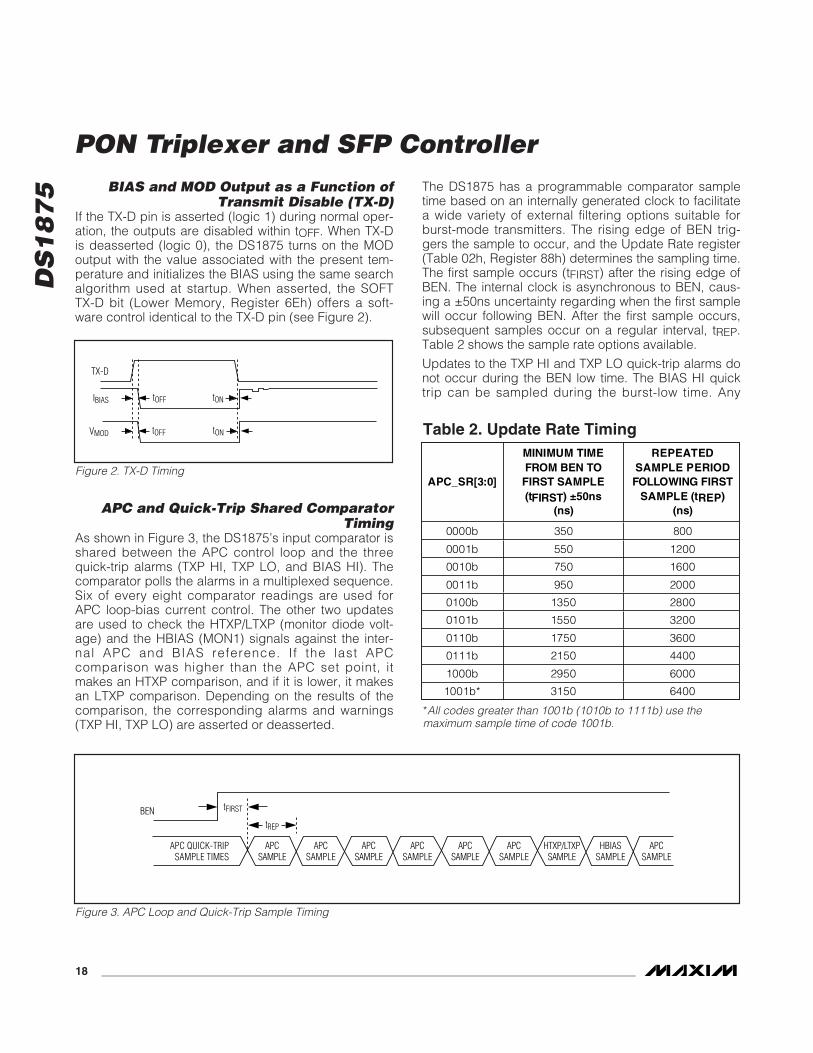
If the TX-D pin is asserted (logic 1) during normal oper-ation, the outputs are disabled within tOFF. When TX-Dis deasserted (logic 0), the DS1875 turns on the MODoutput with the value associated with the present tem-perature and initializes the BIAS using the same searchalgorithm used at startup. When asserted, the SOFTTX-D bit (Lower Memory, Register 6Eh) offers a soft-ware control identical to the TX-D pin (see Figure 2).
APC and Quick-Trip Shared ComparatorTiming
As shown in Figure 3, the DS1875’s input comparator isshared between the APC control loop and the threequick-trip alarms (TXP HI, TXP LO, and BIAS HI). Thecomparator polls the alarms in a multiplexed sequence.Six of every eight comparator readings are used forAPC loop-bias current control. The other two updatesare used to check the HTXP/LTXP (monitor diode volt-age) and the HBIAS (MON1) signals against the inter-nal APC and BIAS reference. If the last APCcomparison was higher than the APC set point, itmakes an HTXP comparison, and if it is lower, it makesan LTXP comparison. Depending on the results of thecomparison, the corresponding alarms and warnings(TXP HI, TXP LO) are asserted or deasserted.
The DS1875 has a programmable comparator sampletime based on an internally generated clock to facilitatea wide variety of external filtering options suitable forburst-mode transmitters. The rising edge of BEN trig-gers the sample to occur, and the Update Rate register(Table 02h, Register 88h) determines the sampling time.The first sample occurs (tFIRST) after the rising edge ofBEN. The internal clock is asynchronous to BEN, caus-ing a ±50ns uncertainty regarding when the first samplewill occur following BEN. After the first sample occurs,subsequent samples occur on a regular interval, tREP.Table 2 shows the sample rate options available.
Updates to the TXP HI and TXP LO quick-trip alarms donot occur during the BEN low time. The BIAS HI quicktrip can be sampled during the burst-low time. Any
*All codes greater than 1001b (1010b to 1111b) use the maximum sample time of code 1001b.
BEN
APC QUICK-TRIPSAMPLE TIMES
HBIASSAMPLE
tFIRST
tREP
HTXP/LTXPSAMPLE
APCSAMPLE
APCSAMPLE
APCSAMPLE
APCSAMPLE
APCSAMPLE
APCSAMPLE
APCSAMPLE
Figure 3. APC Loop and Quick-Trip Sample Timing
Table 2. Update Rate Timing
APC_SR[3:0]
MINIMUM TIME FROM BEN TO FIRST SAMPLE (tFIRST) ±50ns
(ns)
REPEATED SAMPLE PERIOD FOLLOWING FIRST
SAMPLE (tREP)(ns)
0000b 350 800
0001b 550 1200
0010b 750 1600
0011b 950 2000
0100b 1350 2800
0101b 1550 3200
0110b 1750 3600
0111b 2150 4400
1000b 2950 6000
1001b* 3150 6400
TX-D
IBIAS
VMOD tOFF tON
tONtOFF
Figure 2. TX-D Timing

DS
18
75
quick-trip alarm that is detected by default remainsactive until a subsequent comparator sample shows thecondition no longer exists. A second bias-current moni-tor (BIAS MAX) compares the DS1875’s BIAS DAC’scode to a digital value stored in the MAX BIAS register.This comparison is made at every bias-current updateto ensure that a high bias current is quickly detected.
Monitors and Fault DetectionMonitors
Monitoring functions on the DS1875 include a power-onanalog (POA) VCC comparison, five quick-trip com-parators, and ADC channels. This monitoring combinedwith the interrupt masks determine if the DS1875 shutsdown its outputs and triggers the TX-F and FETG out-puts. All the monitoring levels and interrupt masks areuser programmable with the exception of POA, whichtrips at a fixed range and is nonmaskable for safetyreasons.
Power-On Analog (POA)POA holds the DS1875 in reset until VCC is at a suitablelevel (VCC > VPOA) for the part to accurately measurewith its ADC and compare analog signals with its quick-trip monitors. Because VCC cannot be measured by theADC when VCC is less than VPOA, POA also asserts theVCC low alarm, which is cleared by a VCC ADC conver-sion greater than the customer-programmable VCC lowADC limit. This allows a programmable limit to ensurethat the head room requirements of the transceiver aresatisfied during slow power-up. The TX-F and FETGoutputs do not latch until there is a conversion abovethe VCC low limit. The POA alarm is nonmaskable. TheTX-F and FETG outputs are asserted when VCC isbelow VPOA. See the Low-Voltage Operation section formore information.
Five Quick-Trip Monitors and AlarmsFive quick-trip monitors are provided to detect potentiallaser safety issues. These monitor:
1) High Bias Current (HBIAS)
2) Low Transmit Power (LTXP)
3) High Transmit Power (HTXP)
4) Max Output Current (BIAS MAX)
5) MON3 Quick Trip (M3QT)
The high- and low-transmit power quick-trip registers(HTXP and LTXP) set the thresholds used to compareagainst the BMD voltage to determine if the transmitpower is within specification. The HBIAS quick trip com-pares the MON1 input (generally from the MAX3643bias monitor output) against its threshold setting todetermine if the present bias current is above specifica-
tion. The BIAS MAX quick trip is a digital comparisonthat determines if the BIAS DAC indicates that the biascurrent is above specification. IBIAS is not allowed toexceed the value set in the MAX BIAS register. Whenthe DS1875 detects that the bias is at the limit, it setsthe BIAS MAX status bit and clamps the bias current atthe MAX BIAS level. In the closed-loop mode, if therecalled value from the BIAS LUT is greater than MAXBIAS then, the update is not done and IBIAS reverts tothe previous IBIAS value. The quick trips are routed tothe TX-F and FETG outputs through interrupt masks toallow combinations of these alarms to be used to triggerthese outputs. When FETG is triggered, the DS1875 alsodisables the MOD and BIAS outputs. See the BIAS andMOD Output During Power-Up section for details.
MON3 Quick TripOne additional quick trip is used to protect the APDfrom overcurrent. MON3P is used to monitor the currentthrough the APD. When MON3P exceeds a thresholdset by the M3QT DAC register (Table 02h, RegisterC3h), the PWM is shut down by blocking SW pulses.The MON3 comparison is single-ended referenced toground. In the case where MON3 is used differentiallyand not referenced to ground, this must be consideredwhen setting the MON3 quick-trip threshold.Additionally, the D2 pin can be driven either high or lowas determined by INV M3QT and MUX M3QT bits inLower Memory, Register 79h. An external switch con-trolled by pin D2 may be used to clamp the converter’soutput when MON3 quick trip occurs. This externalswitch discharges the output voltage much faster thanallowing the load to discharge the rail. The MON3quick-trip alarm can be latched by enabling M3QT LENin Table 02h, Register 89h. The latch is reset by settingM3QT RESET in Lower Memory, Register 78h. A softquick trip is performed by setting SOFT M3QT in LowerMemory, Register 78h (see Figure 4).
ADC Monitors and AlarmsThe ADC monitors six channels that measure tempera-ture (internal temp sensor), VCC, and MON1–MON4using an analog multiplexer to measure them roundrobin with a single ADC. Each channel has a customer-programmable full-scale range and offset value that isfactory programmed to default value (see Table 3).Additionally, MON1–MON4 can right-shift results by upto 7 bits before the results are compared to alarmthresholds or read over the I2C bus. This allows cus-tomers with specified ADC ranges to calibrate the ADCfull scale to a factor of 1/2n their specified range tomeasure small signals. The DS1875 can then right-shiftthe results by n bits to maintain the bit weight of theirspecification.
PON Triplexer and SFP Controller
______________________________________________________________________________________ 19

DS
18
75
PON Triplexer and SFP Controller
20 ______________________________________________________________________________________
The ADC results (after right-shifting, if used) are com-pared to high and low alarm and warning thresholdsafter each conversion. The alarm values can be used totrigger the TX-F or FETG outputs. These ADC thresholdsare user programmable through the I2C interface, aswell as masking registers that can be used to preventthe alarms from triggering the TX-F and FETG outputs.
ADC TimingThere are 10 analog channels that are digitized in asequential fashion. The MON5–MON8 channels aresampled depending on the state of the EN5TO8B bit inTable 02h, Register 89h. If the bit is programmed tologic 0, the ADC cycles through temperature, VCC, andMON1–MON4 (Figure 5). If the bit is programmed tologic 1, all 10 channels are digitized, including chan-nels MON5–MON8 (Figure 6). In this mode (EN5TO8B= 0), each of MON5–MON8 is sampled on alternatecycles, as shown in Figure 5. The total time required toconvert one set of channels is the sequential ADCcycle time, tFRAME1 or tFRAME2 (see Figure 6).
Table 3. ADC Default Monitor Ranges
SIGNAL+FS
SIGNAL+FS HEX
-FS SIGNAL
-FS HEX
Temperature (°C) 127.996 7FFF -128 8000
VCC (V) 6.5528 FFF8 0 0000
MON1–MON8 (V) 2.4997 FFF8 0 0000
VCC MON1 MON2 MON3 MON4 MON5 MON6TEMP VCC MON1 MON2 MON3 MON4 MON7 MON8TEMP
tFRAME2 tFRAME2
Figure 6. ADC Timing with EN5TO8B = 1
TEMP VCC MON1 MON2 MON3 MON4 TEMP
ONE ADC CYCLE
MON4
tFRAME1
Figure 5. ADC Timing with EN5TO8B = 0
TRIP CONDITION
mCLK(525kHz)
CAPTURE ALARM
M3QT ALARM(UNLATCHED)
Figure 4. M3QT Timing

DS
18
75
Right-Shifting ADC ResultIf the weighting of the ADC digital reading must con-form to a predetermined full-scale value defined by astandard’s specification, then right-shifting can be usedto adjust the predetermined full-scale analog measure-ment range while maintaining the weighting of the ADCresults. The DS1875’s range is wide enough to cover allrequirements; when the maximum input value is ≤ 1/2the FS value, right-shifting can be used to obtaingreater accuracy. For instance, the maximum voltagemight be 1/8th the specified predetermined full-scalevalue, so only 1/8th the converter’s range is used. Analternative is to calibrate the ADC’s full-scale range to1/8th the readable predetermined full-scale value anduse a right-shift value of 3. With this implementation, theresolution of the measurement is increased by a factorof 8, and because the result is digitally divided by 8 byright-shifting, the bit weight of the measurement stillmeets the standard’s specification (i.e., SFF-8472).
The right-shift operation on the ADC result is carried outbased on the contents of RIGHT SHIFT1/0 registers(Table 02h, Registers 8Eh–8Fh). Four analog channels,MON1–MON4, have 3 bits each allocated to set thenumber of right-shifts. Up to seven right-shift operationsare allowed and are executed as a part of every con-version before the results are compared to the high andlow alarm levels, or loaded into their correspondingmeasurement registers (Table 01h, Registers
62h–6Bh). This is true during the setup of internal cali-bration as well as during subsequent data conversions.
Transmit Fault (TX-F) OutputThe TX-F output has masking registers for the ADCalarms and the QT alarms to select which comparisonscause it to assert. In addition, the FETG alarm is selec-table through the TX-F mask to cause TX-F to assert. Allalarms, with the exception of FETG, only cause TX-F toremain active while the alarm condition persists.However, the TX-F latch bit can enable the TX-F outputto remain active until it is cleared by the TX-F reset bit,TX-D, SOFT TX-D, or by power cycling the part. If theFETG output is configured to trigger TX-F, it indicatesthat the DS1875 is in shutdown and requires TX-D,SOFT TX-D, or cycling power to reset. Only enabledalarms activate TX-F (see Figure 7). Table 4 showsTX-F as a function of TX-D and the alarm sources.
Table 4. TX-F as a Function of TX-D andAlarm Sources
VCC > VPOA TX-D NONMASKED TX-F ALARM
TX-F
No X X 1
Yes 0 0 0
Yes 0 1 1
Yes 1 X 0
TX-F LATCHED OPERATION
TX-F NONLATCHED OPERATION
DETECTION OFTX-F FAULT
TX-D ORTX-F RESET
TX-F
DETECTION OFTX-F FAULT
TX-F
Figure 7. TX-F Timing
PON Triplexer and SFP Controller
______________________________________________________________________________________ 21
DS
18
75
PON Triplexer and SFP Controller
22 ______________________________________________________________________________________
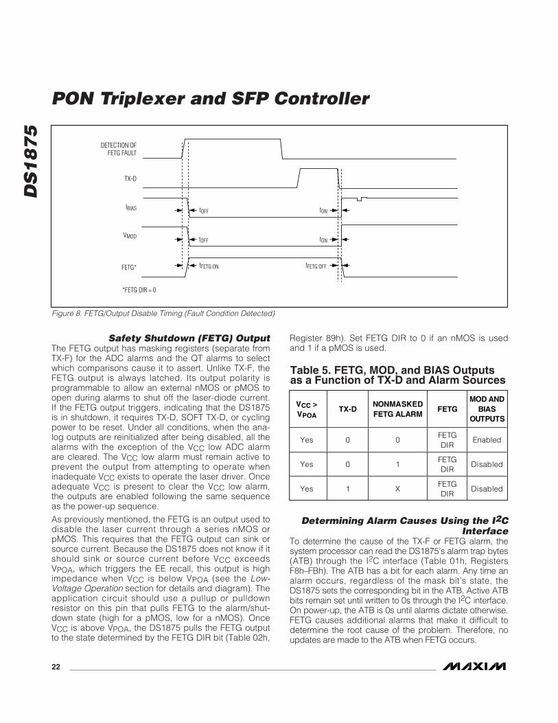
Safety Shutdown (FETG) OutputThe FETG output has masking registers (separate fromTX-F) for the ADC alarms and the QT alarms to selectwhich comparisons cause it to assert. Unlike TX-F, theFETG output is always latched. Its output polarity isprogrammable to allow an external nMOS or pMOS toopen during alarms to shut off the laser-diode current.If the FETG output triggers, indicating that the DS1875is in shutdown, it requires TX-D, SOFT TX-D, or cyclingpower to be reset. Under all conditions, when the ana-log outputs are reinitialized after being disabled, all thealarms with the exception of the VCC low ADC alarmare cleared. The VCC low alarm must remain active toprevent the output from attempting to operate wheninadequate VCC exists to operate the laser driver. Onceadequate VCC is present to clear the VCC low alarm,the outputs are enabled following the same sequenceas the power-up sequence.
As previously mentioned, the FETG is an output used todisable the laser current through a series nMOS orpMOS. This requires that the FETG output can sink orsource current. Because the DS1875 does not know if itshould sink or source current before VCC exceedsVPOA, which triggers the EE recall, this output is highimpedance when VCC is below VPOA (see the Low-Voltage Operation section for details and diagram). Theapplication circuit should use a pullup or pulldownresistor on this pin that pulls FETG to the alarm/shut-down state (high for a pMOS, low for a nMOS). OnceVCC is above VPOA, the DS1875 pulls the FETG outputto the state determined by the FETG DIR bit (Table 02h,
Register 89h). Set FETG DIR to 0 if an nMOS is usedand 1 if a pMOS is used.
Determining Alarm Causes Using the I2CInterface
To determine the cause of the TX-F or FETG alarm, thesystem processor can read the DS1875’s alarm trap bytes(ATB) through the I2C interface (Table 01h, RegistersF8h–FBh). The ATB has a bit for each alarm. Any time analarm occurs, regardless of the mask bit’s state, theDS1875 sets the corresponding bit in the ATB. Active ATBbits remain set until written to 0s through the I2C interface.On power-up, the ATB is 0s until alarms dictate otherwise.FETG causes additional alarms that make it difficult todetermine the root cause of the problem. Therefore, noupdates are made to the ATB when FETG occurs.
IBIAS
VMOD
DETECTION OFFETG FAULT
tOFF tON
tONtOFF
TX-D
tFETG:ONFETG*
*FETG DIR = 0
tFETG:OFF
Figure 8. FETG/Output Disable Timing (Fault Condition Detected)
Table 5. FETG, MOD, and BIAS Outputsas a Function of TX-D and Alarm Sources
VCC > VPOA
TX-DNONMASKED FETG ALARM
FETGMOD AND
BIAS OUTPUTS
Yes 0 0 FETG DIR
Enabled
Yes 0 1 FETG DIR
Disabled
Yes 1 X FETG DIR
Disabled

DS
18
75
Die IdentificationThe DS1875 has an ID hard-coded to its die. Two regis-ters (Table 02h, Registers 86h–87h) are assigned forthis feature. Byte 86h reads 75h to identify the part asthe DS1875; byte 87h reads the die revision.
Low-Voltage OperationThe DS1875 contains two power-on reset (POR) levels.The lower level is a digital POR (VPOD) and the higherlevel is an analog POR (VPOA). At startup, before thesupply voltage rises above VPOA, the outputs are dis-abled (FETG and BIAS outputs are high impedance,MOD is low), all SRAM locations are low (includingshadowed EEPROM (SEE)), and all analog circuitry isdisabled. When VCC reaches VPOA, the SEE isrecalled, and the analog circuitry is enabled. While VCCremains above VPOA, the device is in its normal operat-ing state, and it responds based on its nonvolatile con-figuration. If during operation VCC falls below VPOA butis still above VPOD, the SRAM retains the SEE settingsfrom the first SEE recall, but the device analog is shutdown and the outputs are disabled. FETG is driven toits alarm state defined by the FETG DIR bit (Table 02h,Register 89h). If the supply voltage recovers backabove VPOA, the device immediately resumes normalfunctioning. When the supply voltage falls below VPOD,the device SRAM is placed in its default state andanother SEE recall is required to reload the nonvolatilesettings. The EEPROM recall occurs the next time VCCexceeds VPOA. Figure 9 shows the sequence of eventsas the voltage varies.
Any time VCC is above VPOD, the I2C interface can beused to determine if VCC is below the VPOA level. Thisis accomplished by checking the RDYB bit in the status(Lower Memory, Register 6Eh) byte. RDYB is set whenVCC is below VPOA. When VCC rises above VPOA,RDYB is timed (within 500µs) to go to 0, at which pointthe part is fully functional.
For all device addresses sourced from EEPROM (Table02h, Register 8Ch), the default device address is A2huntil VCC exceeds VPOA, allowing the device addressto be recalled from the EEPROM.
Enhanced RSSI Monitoring (Dual RangeFunctionality)
The DS1875 offers a new feature to improve the accu-racy and range of MON3, which is most commonlyused for monitoring RSSI. This feature enables right-shifting (along with its gain and offset settings) whenthe input signal is below a set threshold (within therange that benefits using right-shifting) and then auto-matically disables right-shifting (recalling different gainand offset settings) when the input signal exceeds thethreshold. Also, to prevent “chattering,” hysteresis pre-vents excessive switching between modes in additionto ensuring that continuity is maintained. Dual rangeoperation is enabled by default (factory programmed inEEPROM). However, it can easily be disabled throughthe RSSI_FF and RSSI_FC bits. When dual range oper-ation is disabled, MON3 operates identically to theother MON channels, although featuring a differentialinput.
VCC
VPOA
VPOD
FETG
SEE
HIGH IMPEDANCE
HIGH IMPEDANCE
HIGH IMPEDANCE
NORMAL OPERATION
DRIVEN TO FETG DIR
NORMALOPERATION
PRECHARGEDTO 0
PRECHARGEDTO 0
PRECHARGEDTO 0
RECALLEDVALUE
RECALLEDVALUE
DRIVEN TO FETG DIR
NORMAL OPERATION
DRIVEN TO FETG DIR
SEE RECALL SEE RECALL
Figure 9. SEE Timing
PON Triplexer and SFP Controller
______________________________________________________________________________________ 23

DS
18
75
24 ______________________________________________________________________________________
Dual-range functionality consists of two modes of opera-tion: fine mode and coarse mode. Each mode is calibrat-ed for a unique transfer function, hence the term, dualrange. Table 6 highlights the registers related to MON3.Fine mode is equivalent to the other MON channels. Finemode is calibrated using the gain, offset, and right-shift-ing registers at locations shown in Table 6 and is idealfor relatively small analog input voltages. Coarse mode isautomatically switched to when the input exceeds thethreshold (to be discussed in a subsequent paragraph).Coarse mode is calibrated using different gain and offsetregisters, but lacks right-shifting (since coarse mode isonly used on large input signals). The gain and offsetregisters for coarse mode are also shown in Table 6.With the use of right-shifting, the fine mode full scale isprogrammed to (1/2N)th the coarse mode full scale. TheDS1875 will now autorange to choose the range thatgives the best resolution for the measurement. To elimi-nate chatter, 6.25% of hysteresis is applied when theinput resides at the boundary of the two ranges. SeeFigure 10. Additional information for each of the registerscan be found in the Memory Map section.
Dual range operation is transparent to the end user. Theresults of MON3 analog-to-digital conversions are stillstored/reported in the same memory locations (68–69h,Lower Memory) regardless of whether the conversionwas performed in fine mode or coarse mode.
When the DS1875 is powered up, analog-to-digital con-versions begin in a round-robin fashion. Every MON3timeslice begins with a fine mode analog-to-digital con-version (using fine mode’s gain, offset, and right-shift-ing settings). See the flowchart in Figure 10. Then,depending on whether the last MON3 timeslice resultedin a coarse-mode conversion and also depending onthe value of the current fine conversion, decisions aremade whether to use the current fine-mode conversionresult or to make an additional conversion (within thesame MON3 timeslice), using coarse mode (usingcoarse mode’s gain and offset settings, and no right-shifting) and reporting the coarse-mode result. Theflowchart also illustrates how hysteresis is implement-ed. The fine-mode conversion is compared to one of
MON3TIMESLICE
END OF MON3TIMESLICE
PERFORM FINE-MODE CONVERSION
REPORT FINECONVERSION RESULT
REPORT COARSECONVERSION RESULT
DID PRIOR MON3TIMESLICE RESULT IN ACOARSE CONVERSION?
(LAST RSSI = 1?)
LAST RSSI = 0 LAST RSSI = 1
WAS CURRENT FINE-MODE CONVERSION
≥ 93.75% OF FS?
PERFORM COARSE-MODE CONVERSION
DID CURRENT FINE-MODE CONVERSION
REACH MAX?
N
Y
YY
N
N
Figure 10. RSSI Flowchart
Table 6. MON3 Configuration RegistersREGISTER FINE MODE COARSE MODE
MON3 FINE SCALE 98h–99h, Table 02h 9Ch–9Dh, Table 02h
MON3 FINE OFFSET A8h–A9h, Table 02h ACh–ADh, Table 02h
RIGHT SHIFT0/1 8Eh–8Fh, Table 02h —
CONFIG (RSSI_FC, RSSI_FF bits) 89h, Table 02h
MON3 VALUE 68h–69h, Lower Memory
PON Triplexer and SFP Controller

DS
18
75
two thresholds. The actual threshold values are a func-tion of the number of right-shifts being used. Table 7shows the threshold values for each possible numberof right-shifts.
The RSSI_FF and RSSI_FC (Table 02h, Register 89h)bits are used to force fine-mode or coarse-mode con-versions, or to disable the dual-range functionality.Dual-range functionality is enabled by default (bothRSSI_FC and RSSI_FF are factory programmed to 0 inEEPROM). It can be disabled by setting RSSI_FC to 0
and RSSI_FF to 1. These bits are also useful when cali-brating MON3. For additional information, see theMemory Map section.
PWM ControllerThe DS1875 has a PWM controller that, when used withexternal components, generates a low-noise, high-volt-age output to bias APDs in optical receivers. Theachievable boost voltage is determined by the externalcomponent selection. Figure 12 shows a typicalschematic. Selection of switching frequency, externalinductor, capacitors, resistor network, switching FET,and switch diode determine the performance of theDC-DC converter. The PWM controller can be config-ured in boost or buck mode. Both modes require anexternal nMOS or npn transistor.
The DS1875 PWM controller consists of several sec-tions used to create a PWM signal to drive a DC-DCconverter. Figure 11 is a block diagram of the DS1875PWM controller. Following is a description of eachblock in the PWM controller and some guidelines forselecting components for the DC-DC converter.
The PWM DAC is used to set the desired output voltageof the DC-DC converter section. The feedback from theDC-DC converter is compared to the output from thePWM DAC by an error amplifier. If the FB level is less
Table 7. MON3 Hysteresis Threshold Values
*This is the minimum reported coarse-mode conversion.
NO. OF RIGHT-SHIFTS
FINE MODE (MAX)
COARSE MODE (MIN*)
0 FFF8h F000h
1 7FFCh 7800h
2 3FFEh 3C00h
3 1FFFh 1E00h
4 0FFFh 0F00h
5 07FFh 0780h
6 03FFh 03C0h
7 01FFh 01E0h
MUXPWM DAC
8-BIT0 TO 1.25V
10μA
MANUAL I2C CONTROL
PWM_FR[1:0]
RAMP
90% DUTYCYCLE OSC
SW
COMP
M3QT
1.9V
1.0V
FB
PWM EN
PWM CONTROLLER
GATE DRIVER90% MAX
DUTY CYCLE
PWM DACTABLE 02h
REGISTER FEh
PWM DAC TEMPERATURE-REFERENCED LUT
TABLE 07h
VOLTAGE CLAMPHIGH = 2.1VLOW = 0.8V
ERRORAMPLIFIER
10μA
DS1875
Figure 11. PWM Controller Diagram
PON Triplexer and SFP Controller
______________________________________________________________________________________ 25

DS
18
75
PON Triplexer and SFP Controller
26 ______________________________________________________________________________________
than the PWM DAC level, the error amplifier increasesthe level on the COMP pin. The level on the COMP pinis compared to the signal from the oscillator and rampgenerator to set the duty cycle that is input to the gatedriver and maximum duty-cycle limiting block. Anincrease on the COMP pin increases the duty cycle.Conversely, if FB is greater than the PWM DAC, thelevel on COMP is decreased, decreasing the dutycycle. The gate driver and maximum duty-cycle blockis used to limit the maximum duty cycle of the PWMcontroller to 90%. This block also disables the PWM dri-ver if an M3QT has resulted from the APD currentexceeding a desired limit.
The output from the PWM DAC is used to control theoutput voltage of the DC-DC converter. The values forthe PWM DAC are recalled from the Table 07h, which isa temperature-indexed LUT. The temperature-indexedvalue from the LUT is written to the PWM DAC register(Table 02h, Register FEh), which updates the setting ofthe PWM DAC. The PWM DAC can also be operated ina manual mode by disabling the automatic updatingfrom the LUT. This is done by clearing the PWM EN bit(Table 02h, Register 80h, Bit 5). The PWM DAC full-scale output is 1.25V with 8 bits of resolution. Whendesigning the feedback for the DC-DC converter sec-tion, the user needs to make sure that the desired levelapplied to the FB pin is in this range.
The COMP pin is driven by the error amplifier compar-ing the PWM DAC to the DC-DC converter feedbacksignal at the FB pin. The error amplifier can sink andsource 10µA. An external resistor and capacitor con-nected to the COMP pin determine the rate of changethe COMP pin. The resistor provides an initial stepwhen the current from the error amplifier changes. Thecapacitor determines how quickly the COMP pincharges to the desired level. The COMP pin has inter-nal voltage clamps that limit the voltage level to a mini-mum of 0.8V and a maximum of 2.1V.
The oscillator and ramp generator create a ramped sig-nal. The frequency of this signal can be 131.25kHz,262.5kHz, 525kHz, or 1050kHz and is set by thePWM_FR[1:0] bits (Table 02h, Register 88h, Bits 5:4).The low level and high level for the ramped signal areapproximately 1.0V and 1.9V, respectively.
The ramped signal is compared to the voltage level onthe COMP pin to determine the duty cycle that is inputto the gate driver and duty-cycle limiting block. WhenCOMP is clamped low at 0.8V, below the level of theramped signal, the comparator outputs a 0% duty-cycle signal to the gate driver block. When COMP isclamped at 2.1V, above the level of the ramped signal,
the comparator outputs a 100% duty-cycle signal to thegate driver and duty-cycle limiting block. The duty-cycle liming block is used to limit the duty cycle of thePWM signal from the SW pin to 90%.
The PWM controller is designed to protect expensiveAPDs against adverse operating conditions while pro-viding optimal bias. The PWM controller monitors photo-diode current to protect APDs under avalancheconditions using the MON3 quick trip. A voltage levelthat is proportional to the APD current can be input tothe MON3 pin. When this voltage exceeds the level setby the M3QT DAC (Table 02h, Register C3h), pulsesfrom the PWM controller are blocked until the fault iscleared. The quick trip can also toggle the digital outputD2. D2 can be connected to an external FET to quicklydischarge the DC-DC converter filter capacitors.
Inductor SelectionOptimum inductor selection depends on input voltage,output voltage, maximum output current, switching fre-quency, and inductor size. Inductors are typically spec-ified by their inductance (L), peak current (IPK), andresistance (LR).
The inductance value is given by:
Where:
VIN = DC-DC converter input voltage
VOUT = Output of DC-DC converter
IOUT(MAX) = Maximum output current delivered
T = Time period of switching frequency (seconds)
D = Duty cycle
η = Estimated power conversion efficiency
The equation for inductance factors in conversion effi-ciency. For inductor calculation purposes, an η of 0.5to 0.75 is usually suitable.
For example, to obtain an output of 80V with a load cur-rent of 1.0mA from an input voltage of 5.0V using themaximum 90% duty cycle and frequency of 1050kHz(T = 952ns), and assuming an efficiency of 0.5, the pre-vious equation yields an L of 120µH, so a 100µH induc-tor would be a suitable value.
The peak inductor current is given by:
IV D T
LPKIN=
× ×
LV D TI VIN
OUT MAX OUT=
× × ××
2 2
2η
( )

DS
18
75
Stability and Compensation Component SelectionThe components connected to the COMP pin (RCOMPand CCOMP) introduce a pole and zero that are neces-sary for stable operation of the PWM controller(Figure 12).
The dominant pole, POLE1, is formed by the outputimpedance of the error amplifier (REA) and CCOMP. Thezero formed by the components on COMP, ZERO1, isselected to cancel POLE2 formed by the output filtercap C3 and output load RLOAD. The additional pole,POLE3, formed by R1 and C3 should be at least adecade past the crossover frequency to not affect sta-bility. The following formulas can be used to calculatethe poles and zero for the application shown inFigure 12.
POLE1 (dominant pole) = 1/(2π × REA × CCOMP)
ZERO1 (compensation zero) = 1/(2π × RCOMP × CCOMP)
POLE2 (output load pole) =
POLE3 (output filter pole) = 1/(2π × R1 × C3)
The DC open-loop gain is given by:
Where:
REA = 260MΩGM = 425µS
RLOAD = Parallel combination of feedback network andload resistance
VOUT = Output of DC-DC converter
VIN = DC-DC converter input voltage
VFB = Feedback voltage at the FB pin
T = Time period of switching frequency (seconds)
L = Inductor value (henries)
DAC1 OutputThe DAC1 output has a full-scale 2.5V range with 8 bitsof resolution, and is programmed through the I2C inter-face. The DAC1 setting is nonvolatile and password-2(PW2) protected.
M4DAC OutputThe M4DAC output has a full-scale 2.5V range with 8bits of resolution, and is controlled by an LUT indexedby the MON4 voltage. The M4DAC LUT (Table 06h) isnonvolatile and PW2 protected. See the MemoryOrganization section for details. The recalled value iseither 16-bit or 32-bit depending on bits DBL_SB andUP_LOWB in Table 02h, Register C7h.
Digital I/O PinsFive digital I/O pins are provided for additional monitor-ing and control. By default the LOSI pin is used to con-vert a standard comparator output for loss of signal(LOSI) to an open-collector output. This means the muxshown on the block diagram by default selects the LOSIpin as the source for the D0 output transistor. The levelof the D0 pin can be read in the STATUS byte (LowerMemory, Register 6Eh) as the LOS STATUS bit. TheLOS STATUS bit reports back the logic level of the D0pin, so an external pullup resistor must be provided forthis pin to output a high level. The LOSI signal can beinverted before driving the open-drain output transistorusing the XOR gate provided. The MUX LOS allows theD0 pin to be used identically to the D1, D2, and D3pins. However, the mux setting (stored in the EEPROM)does not take effect until VCC > VPOA, allowing the EEP-ROM to recall. This requires the LOSI pin to be ground-ed for D0 to act identical to the D1, D2, and D3 pins.
Digital pins D1, D2, and D3 can be used as inputs oroutputs. External pullup resistors must be provided torealize high-logic levels. The DIN byte indicates thelogic levels of these input pins (Lower Memory, Register79h), and the open-drain outputs can be controlledusing the DOUT byte (Lower Memory, Register 78h).When VCC < VPOA, these outputs are high impedance.Once VCC ≥ VPOA, the outputs go to the power-ondefault state stored in the DPU byte (Table 02h, RegisterC0h). The EEPROM-determined default state of the pincan be modified with PW2 access. After the defaultstate has been recalled, the SRAM registers controllingoutputs can be modified without password access. Thisallows the outputs to be used to control serial interfaceswithout wearing out the default EEPROM setting.
D2 can be configured as the output of a quick-trip mon-itor for MON3. The main application is to quickly shutdown the PWM converter and discharge the voltagecreated by the converter. This is shown in the typicalapplication circuit.
AOL G RV V
V VV V
M EAFB IN
OUT IN
OUT IN= × × ××
× −×
−0 85
22. VV
R TLOUT
LOAD××
×⎛
⎝⎜⎞
⎠⎟2
2 12 2 3
× −−
×× × +( )
V VV V R C C
OUT IN
OUT IN LOADπ
PON Triplexer and SFP Controller
______________________________________________________________________________________ 27
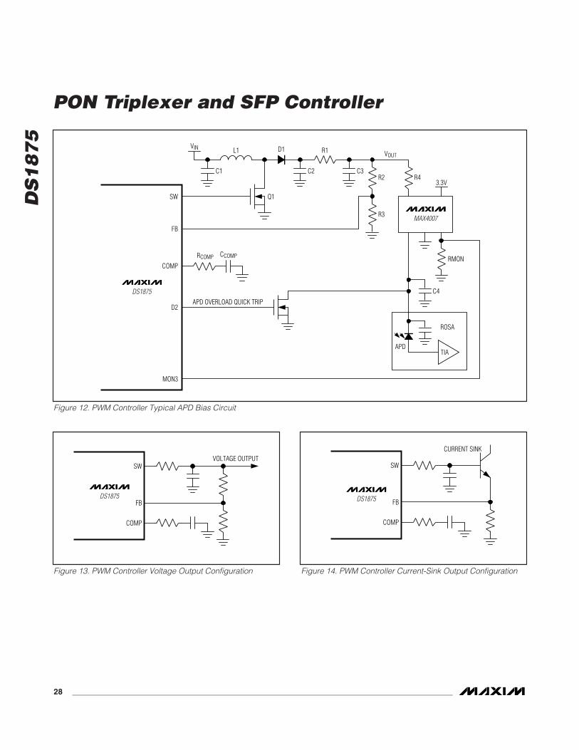
DS
18
75
PON Triplexer and SFP Controller
28 ______________________________________________________________________________________
SW
CURRENT SINK
FB
COMP
DS1875
Figure 14. PWM Controller Current-Sink Output Configuration
SWVOLTAGE OUTPUT
FB
COMP
DS1875
Figure 13. PWM Controller Voltage Output Configuration
COMP
D2
MON3
APD OVERLOAD QUICK TRIP
SW
FB
VIN
C1
Q1
C2R2
R3
RMON
R4
L1
CCOMPRCOMP
D1 R1 VOUT
3.3V
C4
C3
TIA
ROSA
APD
DS1875
MAX4007
Figure 12. PWM Controller Typical APD Bias Circuit

DS
18
75
SCL
NOTE: TIMING IS REFERENCED TO VIL(MAX) AND VIH(MIN).
SDA
STOP START REPEATEDSTART
tBUF
tHD:STA
tHD:DAT tSU:DAT
tSU:STO
tHD:STAtSP
tSU:STAtHIGH
tR
tFtLOW
Figure 15. I2C Timing Diagram
I2C CommunicationI2C Definitions
The following terminology is commonly used todescribe I2C data transfers.
Master Device: The master device controls theslave devices on the bus. The master device gener-ates SCL clock pulses and START and STOP condi-tions.
Slave Devices: Slave devices send and receivedata at the master’s request.
Bus Idle or Not Busy: Time between STOP andSTART conditions when both SDA and SCL are inac-tive and in their logic-high states.
START Condition: A START condition is generatedby the master to initiate a new data transfer with aslave. Transitioning SDA from high to low while SCLremains high generates a START condition. SeeFigure 15 for applicable timing.
STOP Condition: A STOP condition is generated bythe master to end a data transfer with a slave.Transitioning SDA from low to high while SCLremains high generates a STOP condition. SeeFigure 15 for applicable timing.
Repeated START Condition: The master can use arepeated START condition at the end of one datatransfer to indicate that it will immediately initiate anew data transfer fol lowing the current one.Repeated START conditions are commonly usedduring read operations to identify a specific memory
address to begin a data transfer. A repeated STARTcondition is issued identically to a normal STARTcondition. See Figure 15 for applicable timing.
Bit Write: Transitions of SDA must occur during thelow state of SCL. The data on SDA must remain validand unchanged during the entire high pulse of SCLplus the setup and hold-time requirements (Figure15). Data is shifted into the device during the risingedge of the SCL.
Bit Read: At the end of a write operation, the mastermust release the SDA bus line for the proper amountof setup time before the next rising edge of SCL dur-ing a bit read (Figure 15). The device shifts out eachbit of data on SDA at the falling edge of the previousSCL pulse and the data bit is valid at the rising edgeof the current SCL pulse. Remember that the mastergenerates all SCL clock pulses including when it isreading bits from the slave.
Acknowledgement (ACK and NACK): An acknowl-edge-ment (ACK) or not acknowledge (NACK) isalways the 9th bit transmitted during a byte transfer.The device receiving data (the master during a reador the slave during a write operation) performs anACK by transmitting a zero during the 9th bit. Adevice performs a NACK by transmitting a one dur-ing the 9th bit. Timing for the ACK and NACK isidentical to all other bit writes (Figure 15). An ACK isthe acknowledgment that the device is properlyreceiving data. A NACK is used to terminate a readsequence or as an indication that the device is notreceiving data.
PON Triplexer and SFP Controller
______________________________________________________________________________________ 29
DS
18
75
PON Triplexer and SFP Controller
30 ______________________________________________________________________________________
Byte Write: A byte write consists of 8 bits of infor-mation transferred from the master to the slave(most significant bit first) plus a 1-bit acknowledge-ment from the slave to the master. The 8 bits trans-mitted by the master are done according to the bitwrite definition and the acknowledgement is readusing the bit read definition.
Byte Read: A byte read is an 8-bit information trans-fer from the slave to the master plus a 1-bit ACK orNACK from the master to the slave. The 8 bits ofinformation that are transferred (most significant bitfirst) from the slave to the master are read by themaster using the bit read definition, and the mastertransmits an ACK using the bit write definition toreceive additional data bytes. The master mustNACK the last byte read to terminate communicationso the slave returns control of SDA to the master.
Slave Address Byte: Each slave on the I2C busresponds to a slave addressing byte sent immedi-ately following a START condition. The slave addressbyte contains the slave address in the most signifi-cant 7 bits and the R/W bit in the least significant bit.
The DS1875 responds to two slave addresses. Theauxiliary memory always responds to a fixed I2Cslave address, A0h. The Lower Memory and tables00h–08h respond to I2C slave addresses that canbe configured to any value between 00h–FEh usingthe Device Address byte (Table 02h, Register 8Ch).The user also must set the ASEL bit (Table 02h,Register 89h) for this address to be active. By writ-ing the correct slave address with R/W = 0, the mas-ter indicates it will write data to the slave. If R/W = 1,the master reads data from the slave. If an incorrectslave address is written, the DS1875 assumes themaster is communicating with another I2C deviceand ignores the communications until the nextSTART condition is sent. If the main device’s slaveaddress is programmed to be A0h, access to theauxiliary memory is disabled.
Memory Address: During an I2C write operation tothe DS1875, the master must transmit a memoryaddress to identify the memory location where theslave is to store the data. The memory address isalways the second byte transmitted during a writeoperation following the slave address byte.
I2C ProtocolWriting a Single Byte to a Slave: The master mustgenerate a START condition, write the slave addressbyte (R/W = 0), write the memory address, write thebyte of data, and generate a STOP condition. The
master must read the slave’s acknowledgement dur-ing all byte write operations.
Writing Multiple Bytes to a Slave: To write multiplebytes to a slave, the master generates a START con-dition, writes the slave address byte (R/W = 0),writes the memory address, writes up to 8 databytes, and generates a STOP condition. The DS1875writes 1 to 8 bytes (one page or row) with a singlewrite transaction. This is internally controlled by anaddress counter that allows data to be written toconsecutive addresses without transmitting a memo-ry address before each data byte is sent. Theaddress counter limits the write to one 8-byte page(one row of the memory map). Attempts to write toadditional pages of memory without sending a STOPcondition between pages result in the addresscounter wrapping around to the beginning of thepresent row.
Example: A 3-byte write starts at address 06h andwrites three data bytes (11h, 22h, and 33h) to three“consecutive” addresses. The result is that address-es 06h and 07h contain 11h and 22h, respectively,and the third data byte, 33h, is written to address00h.
To prevent address wrapping from occurring, themaster must send a STOP condition at the end ofthe page, then wait for the bus-free or EEPROMwrite time to elapse. Then the master can generate anew START condition and write the slave addressbyte (R/W = 0) and the first memory address of thenext memory row before continuing to write data.
Acknowledge Polling: Any time a EEPROM locationis written, the DS1875 requires the EEPROM writetime (tW) after the STOP condition to write the con-tents of the page to EEPROM. During the EEPROMwrite time, the device does not acknowledge itsslave address because it is busy. It is possible totake advantage of that phenomenon by repeatedlyaddressing the DS1875, which allows the next pageto be written as soon as the DS1875 is ready toreceive the data. The alternative to acknowledgepolling is to wait for a maximum period of tW toelapse before attempting to write again to theDS1875.
EEPROM Write Cycles: When EEPROM writesoccur to the memory, the DS1875 writes the wholeEEPROM memory page, even if only a single byteon the page was modified. Writes that do not modifyall 8 bytes on the page are allowed and do not cor-rupt the remaining bytes of memory on the samepage. Because the whole page is written, bytes that

DS
18
75
were not modified during the transaction are stillsubject to a write cycle. This can result in a wholepage being worn out over time by writing a singlebyte repeatedly. Writing a page one byte at a timewears the EEPROM out eight times faster than writ-ing the entire page at once. The DS1875’s EEPROMwrite cycles are specified in the Nonvolatile MemoryCharacteristics table. The specification shown is atthe worst-case temperature. It can handle approxi-mately 10 times that many writes at room tempera-ture. Writing to SRAM-shadowed EEPROM memorywith SEEB = 1 does not count as a EEPROM writecycle when evaluating the EEPROM’s estimated life-time.
Reading a Single Byte from a Slave: Unlike thewrite operation that uses the memory address byteto define where the data is to be written, the readoperation occurs at the present value of the memoryaddress counter. To read a single byte from theslave, the master generates a START condition,writes the slave address byte with R/W = 1, readsthe data byte with a NACK to indicate the end of thetransfer, and generates a STOP condition.
Manipulating the Address Counter for Reads: Adummy write cycle can be used to force the addresspointer to a particular value. To do this, the mastergenerates a START condition, writes the slaveaddress byte (R/W = 0), writes the memory addresswhere it desires to read, generates a repeatedSTART condition, writes the slave address byte (R/W= 1), reads data with ACK or NACK as applicable,and generates a STOP condition.
Memory MapMemory Organization
The DS1875 features 10 separate memory tables thatare internally organized into 8-byte rows.
The Lower Memory is addressed from 00h to 7Fh andcontains alarm and warning thresholds, flags, masks,several control registers, password entry area (PWE),and the table select byte.
Table 00h contains conversion results for MON5through MON8.
Table 01h primarily contains user EEPROM (with PW1level access) as well as some alarm and warning statusbytes.
Table 02h is a multifunction space that contains config-uration registers, scaling and offset values, passwords,interrupt registers, as well as other miscellaneous con-trol bytes.
Table 03h is strictly user EEPROM that is protected bya PW2-level password.
Table 04h contains a temperature-indexed LUT forcontrol of the modulation voltage. The modulation LUTcan be programmed in 2°C increments over the -40°Cto +102°C range. Access to this register is protectedby a PW2-level password.
Table 05h contains a temperature-indexed LUT thatallows the APC set point to change as a function oftemperature to compensate for Tracking Error (TE). TheAPC LUT has 36 entries that determine the APC settingin 4°C windows between -40°C to 100°C. Access to thisregister is protected by a PW2-level password.
Table 06h contains a MON4-indexed LUT for control ofthe M4DAC voltage. The MON4 LUT has 32 entries thatare configurable to act as one 32-entry LUT of two 16-byte LUTs. When configured as one 32-byte LUT, eachentry corresponds to an increment of 1/32 the full scale.When configured as two 16-byte LUTs, the first 16bytes and the last 16 bytes each correspond to 1/16 fullscale. Either of the two sections is selected with a sep-arate configuration bit. Access to this register is pro-tected by a PW2-level password.
Table 07h contains a temperature-indexed LUT forcontrol of the PWM reference voltage (integration of FBinput). The PWM LUT has 36 entries that determine theAPC setting in 4°C windows between -40°C to +100°C.Access to this register is protected by a PW2-levelpassword.
Table 08h contains a temperature-indexed LUT forcontrol of the BIAS current. The BIAS LUT can be pro-grammed in 2°C increments over the 40°C to +102°Crange. Access to this register is protected by a PW2-level password.
Auxiliary Memory (Device A0h) contains 256 bytes ofEE memory accessible from address 00h–FFh. It isselected with the device address of A0h.
See the Register Descriptions section for a more com-plete detail of each byte’s function, as well as forread/write permissions for each byte.
PON Triplexer and SFP Controller
______________________________________________________________________________________ 31

DS
18
75
PON Triplexer and SFP Controller
32 ______________________________________________________________________________________
Shadowed EEPROMMany NV memory locations (listed within the RegisterDescriptions section) are actually shadowed EEPROMthat are controlled by the SEEB bit in Table 02h, Byte80h.
The DS1875 incorporates shadowed-EEPROM memorylocations for key memory addresses that can be writtenmany times. By default the shadowed-EEPROM bit,SEEB, is not set and these locations act as ordinaryEEPROM. By setting SEEB, these locations function likeSRAM cells, which allow an infinite number of write
cycles without concern of wearing out the EEPROM.This also eliminates the requirement for the EEPROMwrite time, tWR. Because changes made with SEEB dis-abled do not affect the EEPROM, these changes arenot retained through power cycles. The power-on valueis the last value written with SEEB enabled. This func-tion can be used to limit the number of EEPROM writesduring calibration or to change the monitor thresholdsperiodically during normal operation helping to reducethe number of times EEPROM is written. The MemoryMap description indicates which locations are shad-owed EEPROM.
ATB MISC. CONTROLBITS
EEPROM
FFh
I2C SLAVE ADDRESS A0h(FIXED)
00h
FFh
80h
F8h
PW1 LEVEL ACCESSEEPROM
(120 BYTES)
TABLE 01h
AUXILIARY MEMORY
FFh
F7h
D7h
F7h
FFh
80h
89h
NO MEMORY
MON5–MON8 CONV
TABLE 00h
88h80h
F8h
D8h
CONFIGURATION ANDCONTROL
NO MEMORY
TABLE 02h
FFh
80h
PW2 LEVEL ACCESSEEPROM
(128 BYTES)
TABLE 03h
C7h
80h
MODULATIONLUT
TABLE 04h
A3h
80h
APC TE LUT
TABLE 05h
9Fh
80h
M4DAC LUT
TABLE 06h
DEC0
HEX0h
DEC128
HEX80h
255 FFh 255 FFh
A3h
80h
PWM REF LUT
TABLE 07h
C7h
80h
BIASOPEN-LOOP
LUT
TABLE 08h
TABLE SELECT BYTE
PASSWORD ENTRY (PWE)(7Bh–Eh)
PW2 LEVEL ACCESSEEPROM
(48 BYTES)
DIGITAL DIAGNOSTICFUNCTIONS
DIGITAL DIAGNOSTICFUNCTIONS
7Fh
7Ah
5Fh
2Fh
I2C SLAVE ADDRESS A2h(DEFAULT)
00h
30h
60h
LOWER MEMORY
Figure 16. Memory Map

DS
18
75
This register map shows each byte/word (2 bytes) in terms of the row it is on in the memory. The first byte in the row islocated in memory at the row address (hexadecimal) in the leftmost column. Each subsequent byte on the row isone/two memory locations beyond the previous byte/word’s address. A total of 8 bytes are present on each row. Formore information about each of these bytes, see the corresponding register description.
Register Descriptions
Lower Memory Register Map
LOWER MEMORY
WORD 0 WORD 1 WORD 2 WORD 3 ROW (HEX)
ROW NAME BYTE 0/8 BYTE 1/9 BYTE 2/A BYTE 3/B BYTE 4/C BYTE 5/D BYTE 6/E BYTE 7/F
00 <1>THRESHOLD0 TEMP ALARM HI TEMP ALARM LO TEMP WARN HI TEMP WARN LO
08 <1>THRESHOLD1 VCC ALARM HI VCC ALARM LO VCC WARN HI VCC WARN LO
10 <1>THRESHOLD2 MON1 ALARM HI MON1 ALARM LO MON1 WARN HI MON1 WARN LO
18 <1>THRESHOLD3 MON2 ALARM HI MON2 ALARM LO MON2 WARN HI MON2 WARN LO
20 <1>THRESHOLD4 MON3 ALARM HI MON3 ALARM LO MON3 WARN HI MON3 WARN LO
28 <1>THRESHOLD5 MON4 ALARM HI MON4 ALARM LO MON4 WARN HI MON4 WARN LO
30 <1>PW2 EE EE EE EE EE EE EE EE EE
38 <1>PW2 EE EE EE EE EE EE EE EE EE
40 <1>PW2 EE EE EE EE EE EE EE EE EE
48 <1>PW2 EE EE EE EE EE EE EE EE EE
50 <1>PW2 EE EE EE EE EE EE EE EE EE
58 <1>PW2 EE EE EE EE EE EE EE EE EE
60<2>ADC VALUES0
TEMP VALUE VCC VALUE MON1 VALUE MON2 VALUE
68<0>ADC VALUES1
<2>MON3 VALUE <2>MON4 VALUE <2>RESERVED <0>STATUS <3>UPDATE
70<2>ALARM/
WARN ALARM3 ALARM2 ALARM1 ALARM0 WARN3 WARN2 RESERVED RESERVED
78<0>TABLE SELECT
<5>DOUT <2>DIN<6>
RESERVED <6>PWE MSB <6>PWE LSB
<5>TBL SEL
ACCESS CODE
<0> <1> <2> <3> <4> <5> <6> <7> <8> <9> <10> <11>
Read Access
All All All PW2 All N/A PW1 PW2 N/A PW2 All
Write Access
See each bit/byte
separately PW2 N/A All and DS1875
hardware
PW2 + mode
bit All All PW1 PW2 PW2 N/A PW1
PON Triplexer and SFP Controller
______________________________________________________________________________________ 33

DS
18
75
PON Triplexer and SFP Controller
34 ______________________________________________________________________________________
TABLE 00h
WORD 0 WORD 1 WORD 2 WORD 3 ROW (HEX)
ROW NAME BYTE 0/8 BYTE 1/9 BYTE 2/A BYTE 3/B BYTE 4/C BYTE 5/D BYTE 6/E BYTE 7/F
80 <2>ADC VALUES2 MON5 VALUE MON6 VALUE MON7 VALUE MON8 VALUE
88–FF EMPTY EMPTY EMPTY EMPTY EMPTY EMPTY EMPTY EMPTY EMPTY
ACCESS CODE
<0> <1> <2> <3> <4> <5> <6> <7> <8> <9> <10> <11>
Read Access
All All All PW2 All N/A PW1 PW2 N/A PW2 All
Write Access
See each bit/byte
separately PW2 N/A All and DS1875
hardware
PW2 + mode
bit All All PW1 PW2 PW2 N/A PW1
Table 00h Register Map

DS
18
75
TABLE 01h (PW1)
WORD 0 WORD 1 WORD 2 WORD 3 ROW (HEX)
ROW NAME BYTE 0/8 BYTE 1/9 BYTE 2/A BYTE 3/B BYTE 4/C BYTE 5/D BYTE 6/E BYTE 7/F
80 <7>PW1 EE EE EE EE EE EE EE EE EE
88 <7>PW1 EE EE EE EE EE EE EE EE EE
90 <7>PW1 EE EE EE EE EE EE EE EE EE
98 <7>PW1 EE EE EE EE EE EE EE EE EE
A0 <7>PW1 EE EE EE EE EE EE EE EE EE
A8 <7>PW1 EE EE EE EE EE EE EE EE EE
B0 <7>PW1 EE EE EE EE EE EE EE EE EE
B8 <7>PW1 EE EE EE EE EE EE EE EE EE
C0 <7>PW1 EE EE EE EE EE EE EE EE EE
C8 <7>PW1 EE EE EE EE EE EE EE EE EE
D0 <7>PW1 EE EE EE EE EE EE EE EE EE
D8 <7>PW1 EE EE EE EE EE EE EE EE EE
E0 <7>PW1 EE EE EE EE EE EE EE EE EE
E8 <7>PW1 EE EE EE EE EE EE EE EE EE
F0 <7>PW1 EE EE EE EE EE EE EE EE EE
F8<11>ALARM
TRAP ALARM3 ALARM2 ALARM1 ALARM0 WARN3 WARN2 RESERVED RESERVED
Table 01h Register Map
ACCESS CODE
<0> <1> <2> <3> <4> <5> <6> <7> <8> <9> <10> <11>
Read Access
All All All PW2 All N/A PW1 PW2 N/A PW2 All
Write Access
See each bit/byte
separately PW2 N/A All and DS1875
hardware
PW2 + mode
bit All All PW1 PW2 PW2 N/A PW1
PON Triplexer and SFP Controller
______________________________________________________________________________________ 35
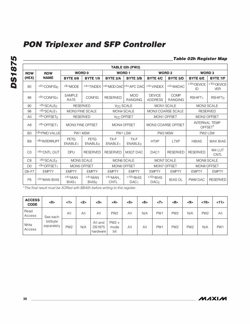
DS
18
75
PON Triplexer and SFP Controller
36 ______________________________________________________________________________________
TABLE 02h (PW2)
WORD 0 WORD 1 WORD 2 WORD 3 ROW (HEX)
ROW NAME BYTE 0/8 BYTE 1/9 BYTE 2/A BYTE 3/B BYTE 4/C BYTE 5/D BYTE 6/E BYTE 7/F
80 <0>CONFIG0 <8>MODE <4>TINDEX <4>MOD DAC <4>APC DAC <4>VINDEX <4>M4DAC<10>DEVICE
ID
<10>DEVICE VER
88 <8>CONFIG1SAMPLE
RATE CONFIG RESERVED
MOD RANGING
DEVICE ADDRESS
COMP RANGING
RSHIFT1 RSHIFT0
90 <8>SCALE0 RESERVED VCC SCALE MON1 SCALE MON2 SCALE
98 <8>SCALE1 MON3 FINE SCALE MON4 SCALE MON3 COARSE SCALE RESERVED
A0 <8>OFFSET0 RESERVED VCC OFFSET MON1 OFFSET MON2 OFFSET
A8 <8>OFFSET1 MON3 FINE OFFSET MON4 OFFSET MON3 COARSE OFFSET INTERNAL TEMP
OFFSET*
B0 <9>PWD VALUE PW1 MSW PW1 LSW PW2 MSW PW2 LSW
B8 <8>INTERRUPT FETG
ENABLE1
FETG ENABLE0
TX-F ENABLE1
TX-F ENABLE0
HTXP LTXP HBIAS MAX BIAS
C0 <8>CNTL OUT DPU RESERVED RESERVED M3QT DAC DAC1 RESERVED RESERVED M4 LUT CNTL
C8 <8>SCALE2 MON5 SCALE MON6 SCALE MON7 SCALE MON8 SCALE
D0 <8>OFFSET1 MON5 OFFSET MON6 OFFSET MON7 OFFSET MON8 OFFSET
D8–F7 EMPTY EMPTY EMPTY EMPTY EMPTY EMPTY EMPTY EMPTY EMPTY
F8 <0>MAN BIAS<4>MAN BIAS1
<4>MAN BIAS0
<4>MAN_ CNTL
<10>BIAS DAC1
<10>BIAS DAC0
BIAS OL PWM DAC RESERVED
Table 02h Register Map
ACCESS CODE
<0> <1> <2> <3> <4> <5> <6> <7> <8> <9> <10> <11>
Read Access
All All All PW2 All N/A PW1 PW2 N/A PW2 All
Write Access
See each bit/byte
separately PW2 N/A All and DS1875
hardware
PW2 + mode
bit All All PW1 PW2 PW2 N/A PW1
*The final result must be XORed with BB40h before writing to this register.

DS
18
75
TABLE 03h (PW2)
WORD 0 WORD 1 WORD 2 WORD 3 ROW (HEX)
ROW NAME BYTE 0/8 BYTE 1/9 BYTE 2/A BYTE 3/B BYTE 4/C BYTE 5/D BYTE 6/E BYTE 7/F
80 <8>PW2 EE EE EE EE EE EE EE EE EE
88 <8>PW2 EE EE EE EE EE EE EE EE EE
90 <8>PW2 EE EE EE EE EE EE EE EE EE
98 <8>PW2 EE EE EE EE EE EE EE EE EE
A0 <8>PW2 EE EE EE EE EE EE EE EE EE
A8 <8>PW2 EE EE EE EE EE EE EE EE EE
B0 <8>PW2 EE EE EE EE EE EE EE EE EE
B8 <8>PW2 EE EE EE EE EE EE EE EE EE
C0 <8>PW2 EE EE EE EE EE EE EE EE EE
C8 <8>PW2 EE EE EE EE EE EE EE EE EE
D0 <8>PW2 EE EE EE EE EE EE EE EE EE
D8 <8>PW2 EE EE EE EE EE EE EE EE EE
E0 <8>PW2 EE EE EE EE EE EE EE EE EE
E8 <8>PW2 EE EE EE EE EE EE EE EE EE
F0 <8>PW2 EE EE EE EE EE EE EE EE EE
F8 <8>PW2 EE EE EE EE EE EE EE EE EE
Table 03h Register Map
ACCESS CODE
<0> <1> <2> <3> <4> <5> <6> <7> <8> <9> <10> <11>
Read Access
All All All PW2 All N/A PW1 PW2 N/A PW2 All
Write Access
See each bit/byte
separately PW2 N/A All and DS1875
hardware
PW2 + mode
bit All All PW1 PW2 PW2 N/A PW1
PON Triplexer and SFP Controller
______________________________________________________________________________________ 37

DS
18
75
PON Triplexer and SFP Controller
38 ______________________________________________________________________________________
TABLE 04h (MODULATION LUT)
WORD 0 WORD 1 WORD 2 WORD 3 ROW (HEX)
ROW NAME BYTE 0/8 BYTE 1/9 BYTE 2/A BYTE 3/B BYTE 4/C BYTE 5/D BYTE 6/E BYTE 7/F
80 <8>LUT4 MOD MOD MOD MOD MOD MOD MOD MOD
88 <8>LUT4 MOD MOD MOD MOD MOD MOD MOD MOD
90 <8>LUT4 MOD MOD MOD MOD MOD MOD MOD MOD
98 <8>LUT4 MOD MOD MOD MOD MOD MOD MOD MOD
A0 <8>LUT4 MOD MOD MOD MOD MOD MOD MOD MOD
A8 <8>LUT4 MOD MOD MOD MOD MOD MOD MOD MOD
B0 <8>LUT4 MOD MOD MOD MOD MOD MOD MOD MOD
B8 <8>LUT4 MOD MOD MOD MOD MOD MOD MOD MOD
C0 <8>LUT4 MOD MOD MOD MOD MOD MOD MOD MOD
ACCESS CODE
<0> <1> <2> <3> <4> <5> <6> <7> <8> <9> <10> <11>
Read Access
All All All PW2 All N/A PW1 PW2 N/A PW2 All
Write Access
See each bit/byte
separately PW2 N/A All and DS1875
hardware
PW2 + mode
bit All All PW1 PW2 PW2 N/A PW1
TABLE 05h (APC TE LUT)
WORD 0 WORD 1 WORD 2 WORD 3 ROW (HEX)
ROW NAME BYTE 0/8 BYTE 1/9 BYTE 2/A BYTE 3/B BYTE 4/C BYTE 5/D BYTE 6/E BYTE 7/F
80 <8>LUT5 APC REF APC REF APC REF APC REF APC REF APC REF APC REF APC REF
88 <8>LUT5 APC REF APC REF APC REF APC REF APC REF APC REF APC REF APC REF
90 <8>LUT5 APC REF APC REF APC REF APC REF APC REF APC REF APC REF APC REF
98 <8>LUT5 APC REF APC REF APC REF APC REF APC REF APC REF APC REF APC REF
A0 <8>LUT5 APC REF APC REF APC REF APC REF RESERVED RESERVED RESERVED RESERVED
Table 05h Register Map
ACCESS CODE
<0> <1> <2> <3> <4> <5> <6> <7> <8> <9> <10> <11>
Read Access
All All All PW2 All N/A PW1 PW2 N/A PW2 All
Write Access
See each bit/byte
separately PW2 N/A All and DS1875
hardware
PW2 + mode
bit All All PW1 PW2 PW2 N/A PW1
Table 04h Register Map

DS
18
75
TABLE 06h (M4DAC LUT)
WORD 0 WORD 1 WORD 2 WORD 3 ROW (HEX)
ROW NAME BYTE 0/8 BYTE 1/9 BYTE 2/A BYTE 3/B BYTE 4/C BYTE 5/D BYTE 6/E BYTE 7/F
80 <8>LUT6 M4DAC M4DAC M4DAC M4DAC M4DAC M4DAC M4DAC M4DAC
88 <8>LUT6 M4DAC M4DAC M4DAC M4DAC M4DAC M4DAC M4DAC M4DAC
90 <8>LUT6 M4DAC M4DAC M4DAC M4DAC M4DAC M4DAC M4DAC M4DAC
98 <8>LUT6 M4DAC M4DAC M4DAC M4DAC M4DAC M4DAC M4DAC M4DAC
ACCESS CODE
<0> <1> <2> <3> <4> <5> <6> <7> <8> <9> <10> <11>
Read Access
All All All PW2 All N/A PW1 PW2 N/A PW2 All
Write Access
See each bit/byte
separately PW2 N/A All and DS1875
hardware
PW2 + mode
bit All All PW1 PW2 PW2 N/A PW1
TABLE 07h (PWM REFERENCE LUT)
WORD 0 WORD 1 WORD 2 WORD 3 ROW (HEX)
ROW NAME BYTE 0/8 BYTE 1/9 BYTE 2/A BYTE 3/B BYTE 4/C BYTE 5/D BYTE 6/E BYTE 7/F
80 <8>LUT7 PWM REF PWM REF PWM REF PWM REF PWM REF PWM REF PWM REF PWM REF
88 <8>LUT7 PWM REF PWM REF PWM REF PWM REF PWM REF PWM REF PWM REF PWM REF
90 <8>LUT7 PWM REF PWM REF PWM REF PWM REF PWM REF PWM REF PWM REF PWM REF
98 <8>LUT7 PWM REF PWM REF PWM REF PWM REF PWM REF PWM REF PWM REF PWM REF
A0 <8>LUT7 PWM REF PWM REF PWM REF PWM REF RESERVED RESERVED RESERVED RESERVED
Table 07h Register Map
ACCESS CODE
<0> <1> <2> <3> <4> <5> <6> <7> <8> <9> <10> <11>
Read Access
All All All PW2 All N/A PW1 PW2 N/A PW2 All
Write Access
See each bit/byte
separately PW2 N/A All and DS1875
hardware
PW2 + mode
bit All All PW1 PW2 PW2 N/A PW1
Table 06h Register Map
PON Triplexer and SFP Controller
______________________________________________________________________________________ 39
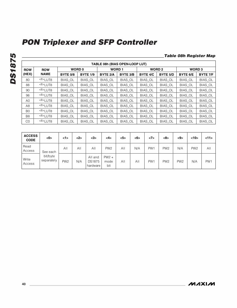
DS
18
75
PON Triplexer and SFP Controller
40 ______________________________________________________________________________________
TABLE 08h (BIAS OPEN-LOOP LUT)
WORD 0 WORD 1 WORD 2 WORD 3 ROW (HEX)
ROW NAME BYTE 0/8 BYTE 1/9 BYTE 2/A BYTE 3/B BYTE 4/C BYTE 5/D BYTE 6/E BYTE 7/F
80 <8>LUT8 BIAS_OL BIAS_OL BIAS_OL BIAS_OL BIAS_OL BIAS_OL BIAS_OL BIAS_OL
88 <8>LUT8 BIAS_OL BIAS_OL BIAS_OL BIAS_OL BIAS_OL BIAS_OL BIAS_OL BIAS_OL
90 <8>LUT8 BIAS_OL BIAS_OL BIAS_OL BIAS_OL BIAS_OL BIAS_OL BIAS_OL BIAS_OL
98 <8>LUT8 BIAS_OL BIAS_OL BIAS_OL BIAS_OL BIAS_OL BIAS_OL BIAS_OL BIAS_OL
A0 <8>LUT8 BIAS_OL BIAS_OL BIAS_OL BIAS_OL BIAS_OL BIAS_OL BIAS_OL BIAS_OL
A8 <8>LUT8 BIAS_OL BIAS_OL BIAS_OL BIAS_OL BIAS_OL BIAS_OL BIAS_OL BIAS_OL
B0 <8>LUT8 BIAS_OL BIAS_OL BIAS_OL BIAS_OL BIAS_OL BIAS_OL BIAS_OL BIAS_OL
B8 <8>LUT8 BIAS_OL BIAS_OL BIAS_OL BIAS_OL BIAS_OL BIAS_OL BIAS_OL BIAS_OL
C0 <8>LUT8 BIAS_OL BIAS_OL BIAS_OL BIAS_OL BIAS_OL BIAS_OL BIAS_OL BIAS_OL
Table 08h Register Map
ACCESS CODE
<0> <1> <2> <3> <4> <5> <6> <7> <8> <9> <10> <11>
Read Access
All All All PW2 All N/A PW1 PW2 N/A PW2 All
Write Access
See each bit/byte
separately PW2 N/A All and DS1875
hardware
PW2 + mode
bit All All PW1 PW2 PW2 N/A PW1

DS
18
75
AUXILIARY MEMORY (A0h)
WORD 0 WORD 1 WORD 2 WORD 3 ROW (HEX)
ROW NAME BYTE 0/8 BYTE 1/9 BYTE 2/A BYTE 3/B BYTE 4/C BYTE 5/D BYTE 6/E BYTE 7/F
00 <5>AUX EE EE EE EE EE EE EE EE EE 08 <5>AUX EE EE EE EE EE EE EE EE EE 10 <5>AUX EE EE EE EE EE EE EE EE EE 18 <5>AUX EE EE EE EE EE EE EE EE EE 20 <5>AUX EE EE EE EE EE EE EE EE EE 28 <5>AUX EE EE EE EE EE EE EE EE EE 30 <5>AUX EE EE EE EE EE EE EE EE EE 38 <5>AUX EE EE EE EE EE EE EE EE EE 40 <5>AUX EE EE EE EE EE EE EE EE EE 48 <5>AUX EE EE EE EE EE EE EE EE EE 50 <5>AUX EE EE EE EE EE EE EE EE EE 58 <5>AUX EE EE EE EE EE EE EE EE EE 60 <5>AUX EE EE EE EE EE EE EE EE EE 68 <5>AUX EE EE EE EE EE EE EE EE EE 70 <5>AUX EE EE EE EE EE EE EE EE EE 78 <5>AUX EE EE EE EE EE EE EE EE EE 80 <5>AUX EE EE EE EE EE EE EE EE EE 88 <5>AUX EE EE EE EE EE EE EE EE EE 90 <5>AUX EE EE EE EE EE EE EE EE EE 98 <5>AUX EE EE EE EE EE EE EE EE EE A0 <5>AUX EE EE EE EE EE EE EE EE EE A8 <5>AUX EE EE EE EE EE EE EE EE EE B0 <5>AUX EE EE EE EE EE EE EE EE EE B8 <5>AUX EE EE EE EE EE EE EE EE EE C0 <5>AUX EE EE EE EE EE EE EE EE EE C8 <5>AUX EE EE EE EE EE EE EE EE EE D0 <5>AUX EE EE EE EE EE EE EE EE EE D8 <5>AUX EE EE EE EE EE EE EE EE EE E0 <5>AUX EE EE EE EE EE EE EE EE EE E8 <5>AUX EE EE EE EE EE EE EE EE EE F0 <5>AUX EE EE EE EE EE EE EE EE EE F8 <5>AUX EE EE EE EE EE EE EE EE EE
Auxiliary A0h Memory Register Map
ACCESS CODE
<0> <1> <2> <3> <4> <5> <6> <7> <8> <9> <10> <11>
Read Access
All All All PW2 All N/A PW1 PW2 N/A PW2 All
Write Access
See each bit/byte
separately PW2 N/A All and DS1875
hardware
PW2 + mode
bit All All PW1 PW2 PW2 N/A PW1
PON Triplexer and SFP Controller
______________________________________________________________________________________ 41

DS
18
75
PON Triplexer and SFP Controller
42 ______________________________________________________________________________________
Lower Memory, Register 02h to 03h: TEMP ALARM LOLower Memory, Register 06h to 07h: TEMP WARN LO
Lower Memory Register DescriptionsLower Memory, Register 00h to 01h: TEMP ALARM HILower Memory, Register 04h to 05h: TEMP WARN HI
FACTORY DEFAULT 7FFFh
READ ACCESS All
WRITE ACCESS PW2
MEMORY TYPE Nonvolatile (SEE)
00h, 04h S 26 25 24 23 22 21 20
01h, 05h 2-1 2-2 2-3 2-4 2-5 2-6 2-7 2-8
BIT 7 BIT 0
Temperature measurement updates above this two’s complement threshold set its corresponding alarm or warning bit. Temperature measurement updates equal to or below this threshold clear its alarm or warning bit.
FACTORY DEFAULT 8000h
READ ACCESS All
WRITE ACCESS PW2
MEMORY TYPE Nonvolatile (SEE)
02h, 06h S 26 25 24 23 22 21 20
03h, 07h 2-1 2-2 2-3 2-4 2-5 2-6 2-7 2-8
BIT 7 BIT 0
Temperature measurement updates below this two’s complement threshold set its corresponding alarm or warning bit. Temperature measurement updates equal to or above this threshold clear its alarm or warning bit.
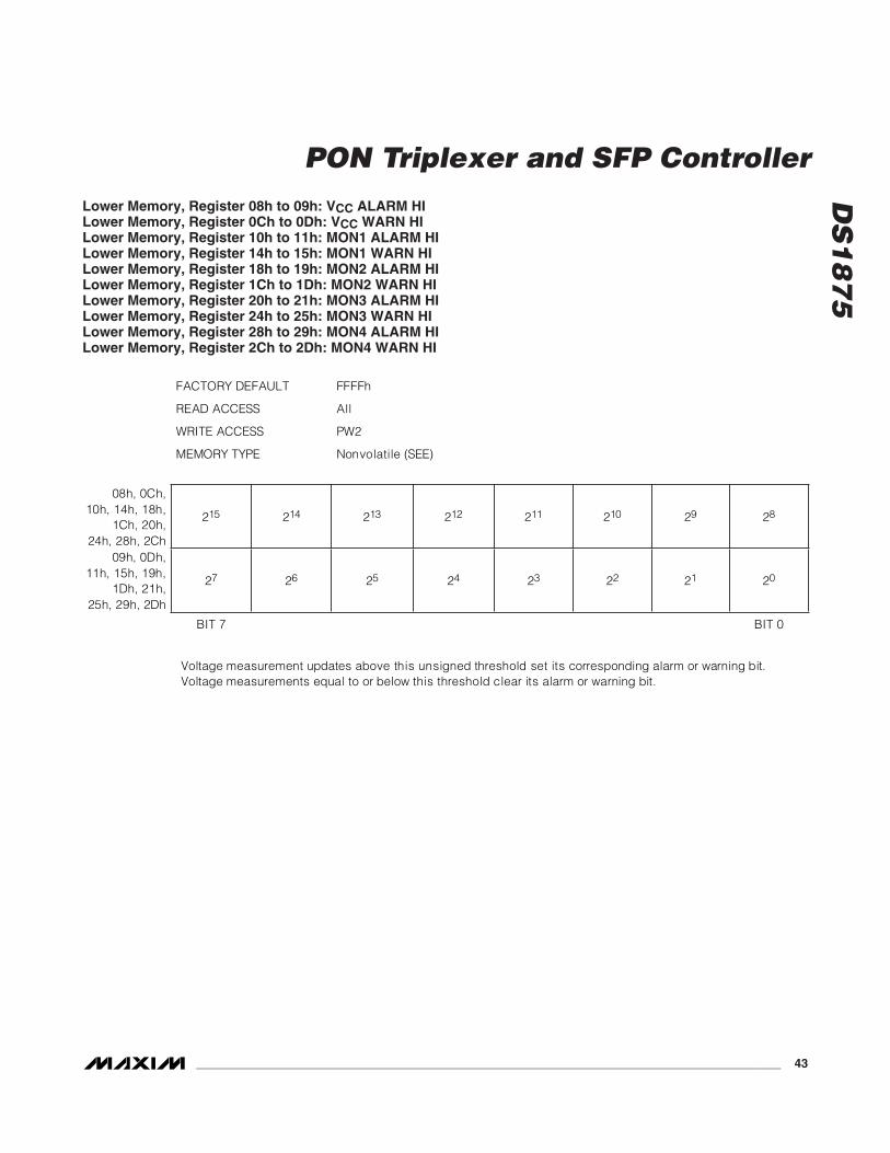
DS
18
75
Lower Memory, Register 08h to 09h: VCC ALARM HILower Memory, Register 0Ch to 0Dh: VCC WARN HILower Memory, Register 10h to 11h: MON1 ALARM HILower Memory, Register 14h to 15h: MON1 WARN HILower Memory, Register 18h to 19h: MON2 ALARM HILower Memory, Register 1Ch to 1Dh: MON2 WARN HILower Memory, Register 20h to 21h: MON3 ALARM HILower Memory, Register 24h to 25h: MON3 WARN HILower Memory, Register 28h to 29h: MON4 ALARM HILower Memory, Register 2Ch to 2Dh: MON4 WARN HI
FACTORY DEFAULT FFFFh
READ ACCESS All
WRITE ACCESS PW2
MEMORY TYPE Nonvolatile (SEE)
08h, 0Ch, 10h, 14h, 18h,
1Ch, 20h, 24h, 28h, 2Ch
215 214 213 212 211 210 29 28
09h, 0Dh, 11h, 15h, 19h,
1Dh, 21h, 25h, 29h, 2Dh
27 26 25 24 23 22 21 20
BIT 7 BIT 0
Voltage measurement updates above this unsigned threshold set its corresponding alarm or warning bit. Voltage measurements equal to or below this threshold clear its alarm or warning bit.
PON Triplexer and SFP Controller
______________________________________________________________________________________ 43

DS
18
75
PON Triplexer and SFP Controller
44 ______________________________________________________________________________________
FACTORY DEFAULT 0000h
READ ACCESS All
WRITE ACCESS PW2
MEMORY TYPE Nonvolatile (SEE)
0Ah, 0Eh, 12h, 16h, 1Ah, 1Eh, 22h, 26h, 2Ah, 2Eh
215 214 213 212 211 210 29 28
0Bh, 0Fh, 13h, 17h, 1Bh, 1Fh, 23h, 27h, 2Bh, 2Fh
27 26 25 24 23 22 21 20
BIT 7 BIT 0
Voltage measurement updates below this unsigned threshold set its corresponding alarm or warning bit. Voltage measurements equal to or above this threshold clear its alarm or warning bit.
Lower Memory, Register 0Ah to 0Bh: VCC ALARM LOLower Memory, Register 0Eh to 0Fh: VCC WARN LOLower Memory, Register 12h to 13h: MON1 ALARM LOLower Memory, Register 16h to 17h: MON1 WARN LOLower Memory, Register 1Ah to 1Bh: MON2 ALARM LOLower Memory, Register 1Eh to 1Fh: MON2 WARN LOLower Memory, Register 22h to 23h: MON3 ALARM LOLower Memory, Register 26h to 27h: MON3 WARN LOLower Memory, Register 2Ah to 2Bh: MON4 ALARM LOLower Memory, Register 2Eh to 2Fh: MON4 WARN LO

DS
18
75
Lower Memory, Register 30h to 5Fh: PW2 EE
FACTORY DEFAULT 00h
READ ACCESS All
WRITE ACCESS PW2
MEMORY TYPE Nonvolatile (EE)
30h to 5Fh EE EE EE EE EE EE EE EE
BIT 7 BIT 0
PW2 level access-controlled EEPROM.
FACTORY DEFAULT 0000h
READ ACCESS All
WRITE ACCESS N/A
MEMORY TYPE Volatile
60h S 26 25 24 23 22 21 20
61h 2-1 2-2 2-3 2-4 2-5 2-6 2-7 2-8
BIT 7 BIT 0
Signed two’s complement direct-to-temperature measurement.
Lower Memory, Register 60h to 61h: TEMP VALUE
PON Triplexer and SFP Controller
______________________________________________________________________________________ 45
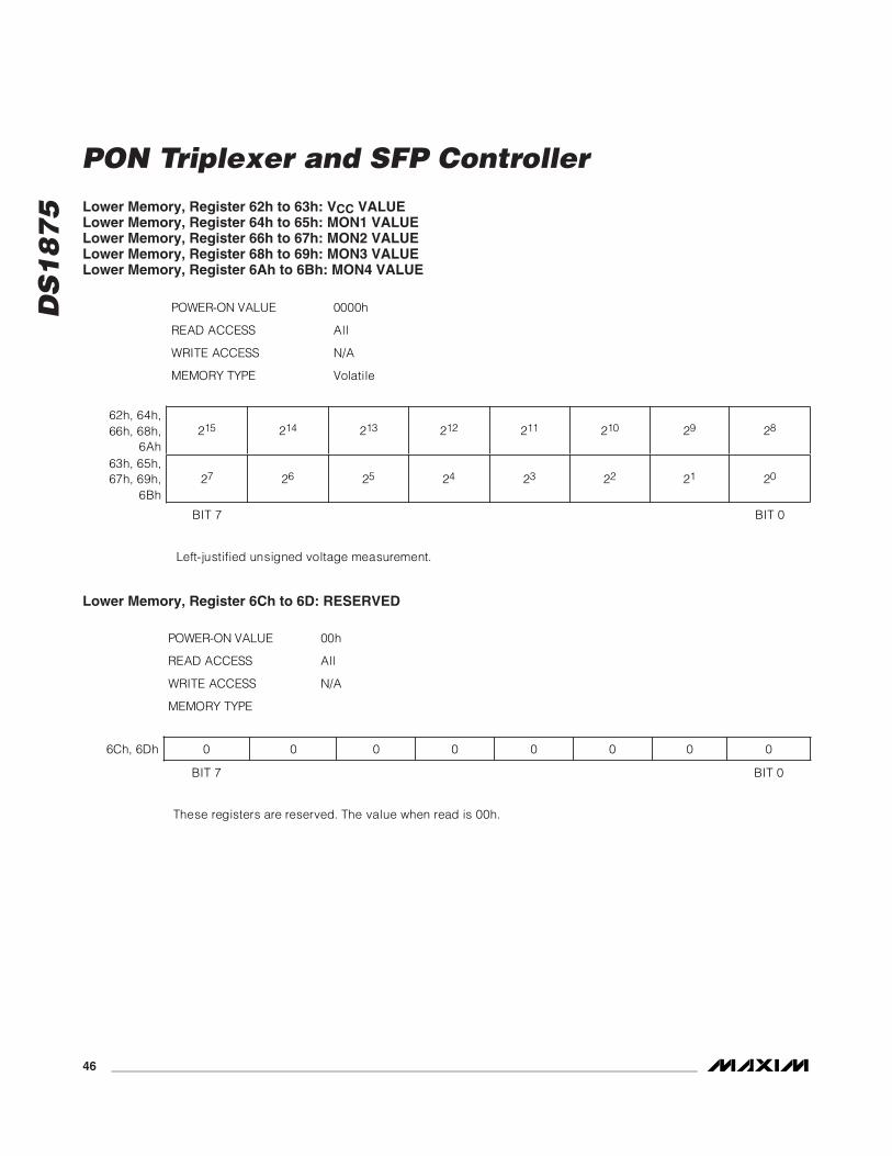
DS
18
75
PON Triplexer and SFP Controller
46 ______________________________________________________________________________________
POWER-ON VALUE 0000h
READ ACCESS All
WRITE ACCESS N/A
MEMORY TYPE Volatile
62h, 64h, 66h, 68h,
6Ah 215 214 213 212 211 210 29 28
63h, 65h, 67h, 69h,
6Bh 27 26 25 24 23 22 21 20
BIT 7 BIT 0
Left-justified unsigned voltage measurement.
POWER-ON VALUE 00h
READ ACCESS All
WRITE ACCESS N/A
MEMORY TYPE
6Ch, 6Dh 0 0 0 0 0 0 0 0
BIT 7 BIT 0
These registers are reserved. The value when read is 00h.
Lower Memory, Register 62h to 63h: VCC VALUELower Memory, Register 64h to 65h: MON1 VALUELower Memory, Register 66h to 67h: MON2 VALUELower Memory, Register 68h to 69h: MON3 VALUELower Memory, Register 6Ah to 6Bh: MON4 VALUE
Lower Memory, Register 6Ch to 6D: RESERVED

DS
18
75
Lower Memory, Register 6Eh: STATUS
POWER-ON VALUE X000 0XXXb
READ ACCESS All
WRITE ACCESS See below
MEMORY TYPE Volatile
Write Access
N/A All N/A All All N/A N/A N/A
6Eh FETG
STATUS SOFT FETG
RESERVED TX-F
RESET SOFT TX-D
TX-F STATUS
LOS STATUS
RDYB
BIT 7 BIT 0
BIT 7
FETG STATUS: Reflects the active state of FETG. The FETG DIR bit in Table 02h, Register 89h defines the polarity of FETG. 0 = Normal operation. Bias and modulation outputs are enabled. 1 = The FETG output is active. Bias and modulation outputs are disabled.
BIT 6 SOFT FETG: 0 = (Default) 1 = Forces the bias and modulation outputs to their off state and assert the FETG output.
BIT 5 RESERVED (Default = 0)
BIT 4 TX-F RESET: 0 = (Default) 1 = Resets the latch for the TX-F output. This bit is self-clearing after resetting TX-F.
BIT 3
SOFT TX-D: This bit allows a software control that is identical to the TX-D pin. See the BIAS and MOD Output as a Function of Transmit Disable (TX-D) section for further information. Its value is wired-ORed with the logic value of the TX-D pin.0 = Internal TX-D signal is equal to the external TX-D pin. 1 = Internal TX-D signal is high.
BIT 2 TX-F STATUS: Reflects the active state of the TX-F pin. 0 = TX-F pin is not active. 1 = TX-F pin is active.
BIT 1 LOS STATUS: Loss of Signal. Reflects the logic level of the LOSI input pin. 0 = LOSI is logic-low. 1 = LOSI is logic-high.
BIT 0 RDBY: Ready Bar. 0 = VCC is above POA. 1 = VCC is below POA and/or too low to communicate over the I2C bus.
PON Triplexer and SFP Controller
______________________________________________________________________________________ 47

DS
18
75
PON Triplexer and SFP Controller
48 ______________________________________________________________________________________
POWER-ON VALUE 00h
READ ACCESS All
WRITE ACCESS All + DS1875 Hardware
MEMORY TYPE Volatile
6Fh TEMP RDY VCC RDY MON1 RDY MON2 RDY MON3 RDY MON4 RDY MON5/7 RDY MON6/8 RDY
BIT 7 BIT 0
Update of completed conversions. At power-on, these bits are cleared and are set as each conversion is completed. These bits can be cleared so that a completion of a new conversion is verified.
Lower Memory, Register 6Fh: UPDATE

DS
18
75
POWER-ON VALUE 10h
READ ACCESS All
WRITE ACCESS N/A
MEMORY TYPE Volatile
70h TEMP HI TEMP LO VCC HI VCC LO MON1 HI MON1 LO MON2 HI MON2 LO
BIT 7 BIT 0
BIT 7 TEMP HI: High alarm status for temperature measurement. 0 = (Default) Last measurement was equal to or below threshold setting. 1 = Last measurement was above threshold setting.
BIT 6 TEMP LO: Low alarm status for temperature measurement.0 = (Default) Last measurement was equal to or above threshold setting. 1 = Last measurement was below threshold setting.
BIT 5 VCC HI: High alarm status for VCC measurement.0 = (Default) Last measurement was equal to or below threshold setting. 1 = Last measurement was above threshold setting.
BIT 4
VCC LO: Low alarm status for VCC measurement. This bit is set when the VCC supply is below the POA trip point value. It clears itself when a VCC measurement is completed and the value is above the low threshold. 0 = Last measurement was equal to or above threshold setting. 1 = (Default) Last measurement was below threshold setting.
BIT 3 MON1 HI: High alarm status for MON1 measurement. 0 = (Default) Last measurement was equal to or below threshold setting. 1 = Last measurement was above threshold setting.
BIT 2 MON1 LO: Low alarm status for MON1 measurement. 0 = (Default) Last measurement was equal to or above threshold setting. 1 = Last measurement was below threshold setting.
BIT 1 MON2 HI: High alarm status for MON2 measurement. 0 = (Default) Last measurement was equal to or below threshold setting. 1 = Last measurement was above threshold setting.
BIT 0 MON2 LO: Low alarm status for MON2 measurement. 0 = (Default) Last measurement was equal to or above threshold setting. 1 = Last measurement was below threshold setting.
Lower Memory, Register 70h: ALARM3
PON Triplexer and SFP Controller
______________________________________________________________________________________ 49

DS
18
75
PON Triplexer and SFP Controller
50 ______________________________________________________________________________________
POWER-ON VALUE 00h
READ ACCESS All
WRITE ACCESS N/A
MEMORY TYPE Volatile
71h MON3 HI MON3 LO MON4 HI MON4 LO RESERVED RESERVED RESERVED RESERVED
BIT 7 BIT 0
BIT 7 MON3 HI: High alarm status for MON3 measurement. 0 = (Default) Last measurement was equal to or below threshold setting. 1 = Last measurement was above threshold setting.
BIT 6 MON3 LO: Low alarm status for MON3 measurement.0 = (Default) Last measurement was equal to or above threshold setting. 1 = Last measurement was below threshold setting.
BIT 5 MON4 HI: High alarm status for MON4 measurement. 0 = (Default) Last measurement was equal to or below threshold setting. 1 = Last measurement was above threshold setting.
BIT 4 MON4 LO: Low alarm status for MON4 measurement.0 = (Default) Last measurement was equal to or above threshold setting. 1 = Last measurement was below threshold setting.
BITS 3:0 RESERVED
Lower Memory, Register 71h: ALARM2

DS
18
75
Lower Memory, Register 72h: ALARM1
POWER-ON VALUE 00h
READ ACCESS All
WRITE ACCESS N/A
MEMORY TYPE Volatile
72h RESERVED RESERVED RESERVED RESERVED BIAS HI RESERVED TXP HI TXP LO
BIT 7 BIT 0
BITS 7:4 RESERVED
BIT 3 BIAS HI: High alarm status bias; fast comparison. 0 = (Default) Last comparison was below threshold setting. 1 = Last comparison was above threshold setting.
BIT 2 RESERVED
BIT 1 TXP HI: High alarm status TXP; fast comparison.0 = (Default) Last comparison was below threshold setting. 1 = Last comparison was above threshold setting.
BIT 0 TXP LO: Low alarm status TXP; fast comparison.0 = (Default) Last comparison was above threshold setting. 1 = Last comparison was below threshold setting.
Lower Memory, Register 73h: ALARM0
POWER-ON VALUE 00h
READ ACCESS All
WRITE ACCESS N/A
MEMORY TYPE Volatile
73h M3QT HI RESERVED RESERVED RESERVED BIAS MAX RESERVED RESERVED RESERVED
BIT 7 BIT 0
BIT 7 M3QT HI: High alarm status for MON3; fast comparison.0 = (Default) Last comparison was below threshold setting. 1 = Last comparison was above threshold setting.
BITS 6:4 RESERVED
BIT 3 BIAS MAX: Alarm status for maximum digital setting of BIAS. 0 = (Default) The value for BIAS is equal to or below the MAX BIAS register. 1 = Requested value for BIAS is greater than the MAX BIAS register.
BITS 2:0 RESERVED
PON Triplexer and SFP Controller
______________________________________________________________________________________ 51

DS
18
75
PON Triplexer and SFP Controller
52 ______________________________________________________________________________________
Lower Memory, Register 74h: WARN3
POWER-ON VALUE 10h
READ ACCESS All
WRITE ACCESS N/A
MEMORY TYPE Volatile
74h TEMP HI TEMP LO VCC HI VCC LO MON1 HI MON1 LO MON2 HI MON2 LO
BIT 7 BIT 0
BIT 7 TEMP HI: High warning status for temperature measurement. 0 = (Default) Last measurement was equal to or below threshold setting. 1 = Last measurement was above threshold setting.
BIT 6 TEMP LO: Low warning status for temperature measurement.0 = (Default) Last measurement was equal to or above threshold setting. 1 = Last measurement was below threshold setting.
BIT 5 VCC HI: High warning status for VCC measurement.0 = (Default) Last measurement was equal to or below threshold setting. 1 = Last measurement was above threshold setting.
BIT 4
VCC LO: Low warning status for VCC measurement. This bit is set when the VCC supply is below the POA trip point value. It clears itself when a VCC measurement is completed and the value is above the low threshold. 0 = Last measurement was equal to or above threshold setting. 1 = (Default) Last measurement was below threshold setting.
BIT 3 MON1 HI: High warning status for MON1 measurement. 0 = (Default) Last measurement was equal to or below threshold setting. 1 = Last measurement was above threshold setting.
BIT 2 MON1 LO: Low warning status for MON1 measurement. 0 = (Default) Last measurement was equal to or above threshold setting. 1 = Last measurement was below threshold setting.
BIT 1 MON2 HI: High warning status for MON2 measurement. 0 = (Default) Last measurement was equal to or below threshold setting. 1 = Last measurement was above threshold setting.
BIT 0 MON2 LO: Low warning status for MON2 measurement. 0 = (Default) Last measurement was equal to or above threshold setting. 1 = Last measurement was below threshold setting.

DS
18
75
Lower Memory, Register 75h: WARN2
POWER-ON VALUE 00h
READ ACCESS All
WRITE ACCESS N/A
MEMORY TYPE Volatile
75h MON3 HI MON3 LO MON4 HI MON4 LO RESERVED RESERVED RESERVED RESERVED
BIT 7 BIT 0
BIT 7 MON3 HI: High warning status for MON3 measurement. 0 = (Default) Last measurement was equal to or below threshold setting. 1 = Last measurement was above threshold setting.
BIT 6 MON3 LO: Low warning status for MON3 measurement.0 = (Default) Last measurement was equal to or above threshold setting. 1 = Last measurement was below threshold setting.
BIT 5 MON4 HI: High warning status for MON4 measurement. 0 = (Default) Last measurement was equal to or below threshold setting. 1 = Last measurement was above threshold setting.
BIT 4 MON4 LO: Low warning status for MON4 measurement.0 = (Default) Last measurement was equal to or above threshold setting. 1 = Last measurement was below threshold setting.
BITS 3:0 RESERVED
Lower Memory Register 76h to 77h: RESERVED MEMORY
POWER-ON VALUE 00h
READ ACCESS All
WRITE ACCESS N/A
MEMORY TYPE
These registers are reserved. The value when read is 00h.
PON Triplexer and SFP Controller
______________________________________________________________________________________ 53

DS
18
75
PON Triplexer and SFP Controller
54 ______________________________________________________________________________________
Lower Memory, Register 78h: DOUT
POWER-ON VALUE Recalled from Table 02h, Register C0h
READ ACCESS All
WRITE ACCESS All
MEMORY TYPE Volatile
78h M3QT RESET
SOFT M3QT
RESERVED RESERVED D3 OUT D2 OUT D1 OUT D0 OUT
BIT 7 BIT 0
BIT 7
M3QT RESET: Resets the latch for M3QT. The PWM does not begin normal operation until the MON3 voltage is below M3QT, regardless of resetting the latch. 0 = (default)1 = M3QT alarm is reset.
BIT 6 SOFT M3QT: Software control for setting the M3QT alarm. The PWM output pulse SW is disabled. 0 = (Default) Internal signal is controlled by trip point comparison. 1 = M3QT alarm is set to 1.
BITS 5:4 RESERVED
BIT 3 D3 OUT: Controls the output of the open-drain pin D3. 0 = Output is held low. 1 = Output is high impedance.
BIT 2 D2 OUT: Controls the output of the open-drain pin D2. 0 = Output is held low. 1 = Output is high impedance.
BIT 1 D1 OUT: Controls the output of the open-drain pin D1. 0 = Output is held low. 1 = Output is high impedance.
BIT 0 D0 OUT: Controls the output of the open-drain pin D0. 0 = Output is held low. 1 = Output is high impedance.
At power-on, these bits are defined by the value stored in the DPU byte (Table 02h, Register C0h). These bits define the value of the logic states of their corresponding output pins.

DS
18
75
Lower Memory, Register 79h: DIN
POWER-ON VALUE See description
READ ACCESS All
WRITE ACCESS N/A
MEMORY TYPE Volatile
79h INV M3QT MUX M3QT INV LOS MUX LOS D3 IN D2 IN D1 IN D0 IN
BIT 7 BIT 0
BIT 7 INV M3QT: Status of inversion of M3QT (internal signal) to D2 pin. MUX M3QT bit must be set to 1 or this bit does not affect the output. The value is controlled (or set) by the DPU byte. 1 = M3QT buffered to D2 is inverted.
BIT 6 MUX M3QT: Determines control of D2 pin. The value is controlled (or set) by the DPU byte. 0 = Logic value of D2 is controlled by DOUT byte. 1 = Logic value of D2 is controlled by M3QT (internal signal) and INV M3QT bit.
BIT 5 INV LOS: Status of inversion of LOSI pin to D0 pin. MUX LOS bit must be set to 1 or this bit does not effect the output. The value is controlled (or set) by the DPU byte. 1 = LOSI buffered D0 is inverted.
BIT 4 MUX LOS: Determines control of D0 pin. The value is controlled (or set) by the DPU byte. 0 = Logic value of D0 is controlled by DOUT byte. 1 = Logic value of D0 is controlled by LOSI pin and INV LOS bit.
BIT 3 D3 IN: Reflects the logic value of D3 pin.
BIT 2 D2 IN: Reflects the logic value of D2 pin.
BIT 1 D1 IN: Reflects the logic value of D1 pin.
BIT 0 D0 IN: Reflects the logic value of D0 pin.
Lower Memory, Register 7Ah: RESERVED
POWER-ON VALUE 00h
READ ACCESS All
WRITE ACCESS N/A
MEMORY TYPE N/A
This register is reserved. The value when read is 00h.
PON Triplexer and SFP Controller
______________________________________________________________________________________ 55

DS
18
75
PON Triplexer and SFP Controller
56 ______________________________________________________________________________________
Lower Memory, Register 7Bh to 7Eh: Password Entry (PWE)
POWER-ON VALUE FFFF FFFFh
READ ACCESS N/A
WRITE ACCESS All
MEMORY TYPE Volatile
7Bh 231 230 229 228 227 226 225 224
7Ch 223 222 221 220 219 218 217 216
7Dh 215 214 213 212 211 210 29 28
7Eh 27 26 25 24 23 22 21 20
BIT 7 BIT 0
There are two passwords for the DS1875. Each password is 4 bytes long. The lower level password (PW1) has all the access of a normal user plus those made available with PW1. The higher level password (PW2) has all the access of PW1 plus those made available with PW2. The values of the passwords reside in EEPROM inside PW2 memory. At power-up, all PWE bits are set to 1. All reads at this location are 0.
Lower Memory, Register 7Fh: Table Select (TBL SEL)
POWER-ON VALUE 00h
READ ACCESS All
WRITE ACCESS All
MEMORY TYPE Volatile
7Fh 27 26 25 24 23 22 21 20
BIT 7 BIT 0
The upper memory tables (Table 00h to 08h) of the DS1875 are accessible by writing the desired table value in this register.

DS
18
75
Table 00h Register DescriptionsTable 00h, Register 80h to 81h: MON5 VALUETable 00h, Register 82h to 83h: MON6 VALUETable 00h, Register 84h to 85h: MON7 VALUETable 00h, Register 86h to 87h: MON8 VALUE
POWER-ON VALUE 0000h
READ ACCESS All
WRITE ACCESS N/A
MEMORY TYPE Volatile
80h, 82h, 84h, 86h
215 214 213 212 211 210 29 28
81h, 83h, 85h, 87h
27 26 25 24 23 22 21 20
BIT 7 BIT 0
Left-justified unsigned voltage measurement.
Table 01h Register DescriptionsTable 01h, Register 80h to F7h: PW1 EEPROM
POWER-ON VALUE 00h
READ ACCESS PW1
WRITE ACCESS PW1
MEMORY TYPE Nonvolatile (EE)
80h to F7h EE EE EE EE EE EE EE EE
BIT 7 BIT 0
EEPROM for PW1-level access.
PON Triplexer and SFP Controller
______________________________________________________________________________________ 57

DS
18
75
PON Triplexer and SFP Controller
58 ______________________________________________________________________________________
Table 01h, Register F8h: ALARM3
POWER-ON VALUE 00h
READ ACCESS All
WRITE ACCESS PW1
MEMORY TYPE Volatile
F8h TEMP HI TEMP LO VCC HI VCC LO MON1 HI MON1 LO MON2 HI MON2 LO
BIT 7 BIT 0
Layout is identical to ALARM3 in Lower Memory, Register 70h with two exceptions. 1. VCC LO alarm is not set at power-on. 2. These bits are latched. They are cleared by power-down or a write with PW1 access.
Table 01h, Register F9h: ALARM2
POWER-ON VALUE 00h
READ ACCESS All
WRITE ACCESS PW1
MEMORY TYPE Volatile
F9h MON3 HI MON3 LO MON4 HI MON4 LO RESERVED RESERVED RESERVED RESERVED
BIT 7 BIT 0
Layout is identical to ALARM2 in Lower Memory, Register 71h with one exception. 1. These bits are latched. They are cleared by power-down or a write with PW1 access.
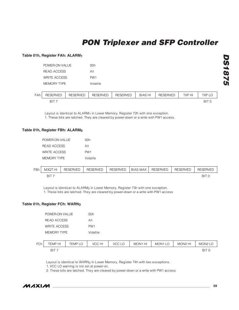
DS
18
75
Table 01h, Register FAh: ALARM1
POWER-ON VALUE 00h
READ ACCESS All
WRITE ACCESS PW1
MEMORY TYPE Volatile
FAh RESERVED RESERVED RESERVED RESERVED BIAS HI RESERVED TXP HI TXP LO
BIT 7 BIT 0
Layout is identical to ALARM1 in Lower Memory, Register 72h with one exception. 1. These bits are latched. They are cleared by power-down or a write with PW1 access.
Table 01h, Register FBh: ALARM0
POWER-ON VALUE 00h
READ ACCESS All
WRITE ACCESS PW1
MEMORY TYPE Volatile
FBh M3QT HI RESERVED RESERVED RESERVED BIAS MAX RESERVED RESERVED RESERVED
BIT 7 BIT 0
Layout is identical to ALARM0 in Lower Memory, Register 73h with one exception. 1. These bits are latched. They are cleared by power-down or a write with PW1 access
Table 01h, Register FCh: WARN3
POWER-ON VALUE 00h
READ ACCESS All
WRITE ACCESS PW1
MEMORY TYPE Volatile
FCh TEMP HI TEMP LO VCC HI VCC LO MON1 HI MON1 LO MON2 HI MON2 LO
BIT 7 BIT 0
Layout is identical to WARN3 in Lower Memory, Register 74h with two exceptions. 1. VCC LO warning is not set at power-on. 2. These bits are latched. They are cleared by power-down or a write with PW1 access.
PON Triplexer and SFP Controller
______________________________________________________________________________________ 59

DS
18
75
PON Triplexer and SFP Controller
60 ______________________________________________________________________________________
Table 01h, Register FDh: WARN2
POWER-ON VALUE 00h
READ ACCESS All
WRITE ACCESS PW1
MEMORY TYPE Volatile
FDh MON3 HI MON3 LO MON4 HI MON4 LO RESERVED RESERVED RESERVED RESERVED
BIT 7 BIT 0
Layout is identical to WARN2 in Lower Memory, Register 75h with one exception. 1. These bits are latched. They are cleared by power-down or a write with PW1 access.
Table 01h, Register FEh to FFh: RESERVED
POWER-ON VALUE 00h
READ ACCESS All
WRITE ACCESS PW1
MEMORY TYPE Volatile
These registers are reserved.

DS
18
75
Table 02h Register DescriptionsTable 02h, Register 80h: MODE
PON Triplexer and SFP Controller
______________________________________________________________________________________ 61
POWER-ON VALUE 3Fh
READ ACCESS PW2
WRITE ACCESS PW2
MEMORY TYPE Volatile
80h SEEB RESERVED PWM EN M4DAC EN AEN MOD EN APC EN BIAS EN
BIT 7 BIT 0
BIT 7
SEEB: 0 = (Default) Enables EEPROM writes to SEE bytes. 1 = Disables EEPROM writes to SEE bytes during configuration, so that the configuration of the part is not delayed by the EE cycle time. Once the values are known, write this bit to a 0 and write the SEE locations again for data to be written to the EEPROM.
BIT 6 RESERVED
BIT 5
PWM EN: 0 = PWM DAC is writable by the user and the LUT recalls are disabled. This allows users to interactively test their modules by writing the DAC value for the PWM DAC. The output is updated with the new value at the end of the write cycle. The I2C STOP condition is the end of the write cycle. 1 = (Default) Enables auto control of the LUT for PWM DAC.
BIT 4
M4DAC EN: 0 = M4DAC is writable by the user and the LUT recalls are disabled. This allows users to interactively test their modules by writing the DAC value for M4DAC. The output is updated with the new value at the end of the write cycle. The I2C STOP condition is the end of the write cycle. 1 = (Default) Enables auto control of the LUT for M4DAC.
BIT 3
AEN: 0 = The temperature-calculated index value TINDEX is writable by users and the updates of calculated indexes are disabled. This allows users to interactively test their modules by controlling the indexing for the LUTs. The recalled values from the LUTs appear in the DAC registers after the next completion of a temperature conversion.
BIT 2
MOD EN: 0 = MOD DAC is writable by the user and the LUT recalls are disabled. This allows users to interactively test their modules by writing the DAC value for modulation. The output is updated with the new value at the end of the write cycle. The I2C STOP condition is the end of the write cycle. 1 = (Default) Enables auto control of the LUT for modulation.
BIT 1
APC EN: 0 = APC DAC is writable by the user and the LUT recalls are disabled. This allows users to interactively test their modules by writing the DAC value for APC reference. The output is updated with the new value at the end of the write cycle. The I2C STOP condition is the end of the write cycle. 1 = (Default) Enables auto control of the LUT for APC reference.
BIT 0
BIAS EN: 0 = BIAS DAC is controlled by the user and the APC is in manual mode. The BIAS DAC value is written to the MAN BIAS register. All values that are written to MAN BIAS and are greater than the MAX BIAS register setting are not updated and set the BIAS MAX alarm bit. The BIAS DAC register continues to reflect the value of the BIAS DAC. This allows users to interactively test their modules by writing the DAC value for bias. The output is updated with the new value at the end of the write cycle to the MAN BIAS register. The I2C STOP condition is the end of the write cycle. 1 = (Default) Enables auto control for the APC feedback.

DS
18
75
PON Triplexer and SFP Controller
62 ______________________________________________________________________________________
Table 02h, Register 81h: Temperature Index (TINDEX)
FACTORY DEFAULT 00h
READ ACCESS PW2
WRITE ACCESS PW2 and AEN = 0
MEMORY TYPE Volatile
81h 27 26 25 24 23 22 21 20
BIT 7 BIT 0
Holds the calculated index based on the temperature measurement. This index is used for the address during lookup of Tables 04h, 05h, 07h, and 08h. Temperature measurements below -40°C or above +102°C are clamped to 00h and C7h, respectively. The calculation of TINDEX is as follows:
TINDEX =Temp_ Value + 40°C
2°C+ 80h
For the temperature-indexed LUTs, the index used during the lookup function for each table is as follows:
Table 04h (MOD) 1 TINDEX6 TINDEX5 TINDEX4 TINDEX3 TINDEX2 TINDEX1 TINDEX0
Table 05h (APC) 1 0 TINDEX6 TINDEX5 TINDEX4 TINDEX3 TINDEX2 TINDEX1
Table 07h (PWM) 1 0 TINDEX6 TINDEX5 TINDEX4 TINDEX3 TINDEX2 TINDEX1
Table 08h (BIAS) 1 TINDEX6 TINDEX5 TINDEX4 TINDEX3 TINDEX2 TINDEX1 TINDEX0
Table 02h, Register 82h: MOD DAC
FACTORY DEFAULT 00h
READ ACCESS PW2
WRITE ACCESS PW2 and MOD EN = 0
MEMORY TYPE Volatile
82h 27 26 25 24 23 22 21 20
BIT 7 BIT 0
The digital value used for MOD and recalled from Table 04h at the adjusted memory address found in TINDEX. This register is updated at the end of the temperature conversion.
VMOD =Full Scale
255MOD DAC

DS
18
75
Table 02h, Register 83h: APC DAC
FACTORY DEFAULT 00h
READ ACCESS PW2
WRITE ACCESS PW2 and APC EN = 0
MEMORY TYPE Volatile
83h 27 26 25 24 23 22 21 20
BIT 7 BIT 0
The digital value used for APC reference and recalled from Table 05h at the adjusted memory address found in TINDEX. This register is updated at the end of the temperature conversion.
VBMD =Full Scale
255APC DAC
Table 02h, Register 84h: Voltage Index (VINDEX)
FACTORY DEFAULT 00h
READ ACCESS PW2
WRITE ACCESS PW2 and AEN = 0
MEMORY TYPE Volatile
84h 27 26 25 24 23 22 21 20
BIT 7 BIT 0
Holds the calculated index based on the MON4 voltage measurement. This index is used for the address during lookup of Table 06h. M4DAC LUT is 32 bytes from address 80h to 9Fh. The calculation of VINDEX is as follows:
VINDEX =MON4800h
+ 80h
When configured as a single LUT, all 32 bytes are used for lookup. When configured as a double LUT, the first 16 bytes (80h to 8Fh) form the lower LUT and the last 16 bytes (90h to 9Fh) form the upper LUT. For the three different modes, the index used during the lookup function of Table 06h is as follows:
Single 1 0 0 VINDEX4 VINDEX3 VINDEX2 VINDEX1 VINDEX0Double/Lower 1 0 0 0 VINDEX4 VINDEX3 VINDEX2 VINDEX1Double/Upper 1 0 0 1 VINDEX4 VINDEX3 VINDEX2 VINDEX1
PON Triplexer and SFP Controller
______________________________________________________________________________________ 63

DS
18
75
PON Triplexer and SFP Controller
64 ______________________________________________________________________________________
Table 02h, Register 85h: M4DAC
FACTORY DEFAULT 00h
READ ACCESS PW2
WRITE ACCESS PW2 and M4DAC EN = 0
MEMORY TYPE Volatile
85h 27 26 25 24 23 22 21 20
BIT 7 BIT 0
The digital value used for M4DAC and recalled from Table 06h at the adjusted memory address found in VINDEX. This register is updated at the end of the MON4 conversion.
VM4DAC =2.5256
(M4DAC +1)
Table 02h, Register 86h: DEVICE ID
FACTORY DEFAULT 75h
READ ACCESS PW2
WRITE ACCESS N/A
MEMORY TYPE ROM
86h 0 1 1 1 0 1 0 1
BIT 7 BIT 0
Hardwired connections to show the device ID.
Table 02h, Register 87h: DEVICE VER
FACTORY DEFAULT DEVICE VERSION
READ ACCESS PW2
WRITE ACCESS N/A
MEMORY TYPE ROM
87h DEVICE VERSION
BIT 7 BIT 0
Hardwired connections to show device version.
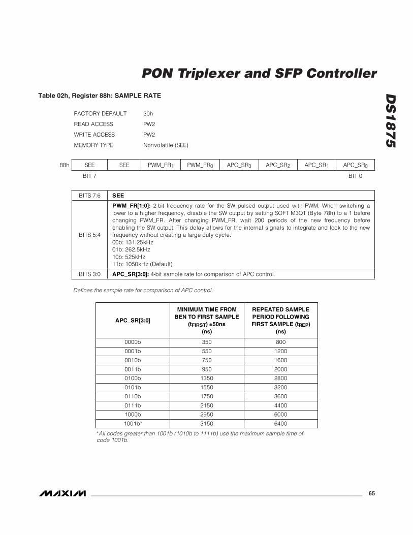
DS
18
75
Table 02h, Register 88h: SAMPLE RATE
FACTORY DEFAULT 30h
READ ACCESS PW2
WRITE ACCESS PW2
MEMORY TYPE Nonvolatile (SEE)
88h SEE SEE PWM_FR1 PWM_FR0 APC_SR3 APC_SR2 APC_SR1 APC_SR0
BIT 7 BIT 0
BITS 7:6 SEE
BITS 5:4
PWM_FR[1:0]: 2-bit frequency rate for the SW pulsed output used with PWM. When switching a lower to a higher frequency, disable the SW output by setting SOFT M3QT (Byte 78h) to a 1 before changing PWM_FR. After changing PWM_FR, wait 200 periods of the new frequency before enabling the SW output. This delay allows for the internal signals to integrate and lock to the new frequency without creating a large duty cycle. 00b: 131.25kHz 01b: 262.5kHz 10b: 525kHz 11b: 1050kHz (Default)
BITS 3:0 APC_SR[3:0]: 4-bit sample rate for comparison of APC control.
APC_SR[3:0]
MINIMUM TIME FROM BEN TO FIRST SAMPLE
(tFIRST) ±50ns (ns)
REPEATED SAMPLE PERIOD FOLLOWING FIRST SAMPLE (tREP)
(ns)
0000b 350 800
0001b 550 1200
0010b 750 1600
0011b 950 2000
0100b 1350 2800
0101b 1550 3200
0110b 1750 3600
0111b 2150 4400
1000b 2950 6000
1001b* 3150 6400
Defines the sample rate for comparison of APC control.
*All codes greater than 1001b (1010b to 1111b) use the maximum sample time ofcode 1001b.
PON Triplexer and SFP Controller
______________________________________________________________________________________ 65

DS
18
75
PON Triplexer and SFP Controller
66 ______________________________________________________________________________________
Table 02h, Register 89h: CONFIG
FACTORY DEFAULT 00h
READ ACCESS PW2
WRITE ACCESS PW2
MEMORY TYPE Nonvolatile (SEE)
89h FETG DIR TX-F LEN M3QT LEN ASEL BOLFS RSSI_FC RSSI_FF EN5TO8B
BIT 7 BIT 0
Configure the memory location and the polarity of the digital outputs.
BIT 7 FETG DIR: Chooses the direction or polarity of the FETG output for normal operation. 0 = (Default) Under normal operation, FETG is pulled low. 1 = Under normal operation, FETG is pulled high.
BIT 6
TX-F LEN: The TX-F output pin always reflects the wired-OR of all TX-F enabled alarm states. This bit enables the latching of the alarm state for the TX-F output pin. 0 = (Default) Not latched. 1 = The alarm bits are latched until cleared by a TX-D transition or power-down. If the VCC alarm is enabled for either FETG or TX-F, then latching is disabled until after the first VCC measurement is made above the VCC ALARM LO set point to allow for proper operation during slow power-on cycles.
BIT 5 M3QT LEN: This bit enables the latching of the alarm for the M3QT. 0 = (Default) Not latched. 1 = The alarm bit is latched until cleared by setting the M3QT RESET bit (Byte 78h).
BIT 4 ASEL: Address select. 0 = (Default) Device address of A2h. 1 = Device address is equal to the value found in the DEVICE ADDRESS byte (Table 02h, 8Ch).
BIT 3 BOLFS: Bias open-loop full scale.0 = (Default) Full scale is 600μA. 1 = Full scale is 1.2mA.
BITS 2:1
RSSI_FC and RSSI_FF: RSSI force coarse and RSSI force fine. Control bits for RSSI mode of operation on the MON3 conversion. 00b = (Default) Normal RSSI mode of operation. 01b = The fine settings of scale and offset are used for MON3 conversions. 10b = The coarse settings of scale and offset are used for MON3 conversions. 11b = Normal RSSI mode of operation.
BIT 0 EN5TO8B: This bit enables MON5–MON8 conversion (voltage of D0–D3 pins). 0 = (Default) Temperature, VCC, and MON1–MON8 conversions are enabled. 1 = Temperature, VCC, and MON1–MON4 conversions are enabled.

DS
18
75
Table 02h, Register 8Ah: RESERVED
FACTORY DEFAULT 00h
READ ACCESS PW2
WRITE ACCESS PW2
MEMORY TYPE Nonvolatile (SEE)
This register is reserved.
Table 02h, Register 8Bh: MOD RANGING
FACTORY DEFAULT 00h
READ ACCESS PW2
WRITE ACCESS PW2
MEMORY TYPE Nonvolatile (SEE)
8Bh RESERVED RESERVED RESERVED RESERVED RESERVED MOD2 MOD1 MOD0
BIT 7 BIT 0
The lower nibble of this byte controls the full-scale range of the Modulation DAC
BITS 7:3 RESERVED (Default = 0)
BITS 2:0
MOD[2:0]: MOD FS RANGING: 3-bit value to select the FS output voltage for MOD. Default is 000b and creates a FS of 1.25V.
MOD[2:0] % OF 1.25V FS VOLTAGE (V)000b 100.00 1.250 001b 80.05 1.001 010b 66.75 0.834 011b 50.13 0.627 100b 40.15 0.502 101b 33.50 0.419 110b 28.74 0.359 111b 25.17 0.315
PON Triplexer and SFP Controller
______________________________________________________________________________________ 67

DS
18
75
PON Triplexer and SFP Controller
68 ______________________________________________________________________________________
Table 02h, Register 8Ch: DEVICE ADDRESS
FACTORY DEFAULT 00h
READ ACCESS PW2
WRITE ACCESS PW2
MEMORY TYPE Nonvolatile (SEE)
8Ch 27 26 25 24 23 22 21 20
BIT 7 BIT 0
This value becomes the I2C slave address for the main memory when the ASEL (Table 02h, Register 89h) bit is set. If A0h is programmed to this register, the auxiliary memory is disabled.
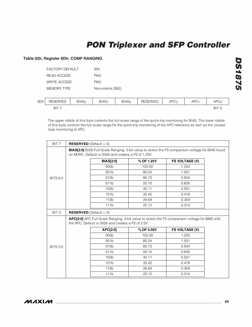
DS
18
75
Table 02h, Register 8Dh: COMP RANGING
FACTORY DEFAULT 00h
READ ACCESS PW2
WRITE ACCESS PW2
MEMORY TYPE Nonvolatile (SEE)
8Dh RESERVED BIAS2 BIAS1 BIAS0 RESERVED APC2 APC1 APC0
BIT 7 BIT 0
The upper nibble of this byte controls the full-scale range of the quick-trip monitoring for BIAS. The lower nibble of this byte controls the full-scale range for the quick-trip monitoring of the APC reference as well as the closed-loop monitoring of APC.
BIT 7 RESERVED (Default = 0)
BITS 6:4
BIAS[2:0] BIAS Full-Scale Ranging. 3-bit value to select the FS comparison voltage for BIAS found on MON1. Default is 000b and creates a FS of 1.25V.
BIAS[2:0] % OF 1.25V FS VOLTAGE (V)
000b 100.00 1.250
001b 80.04 1.001
010b 66.73 0.834
011b 50.10 0.626
100b 40.11 0.501
101b 33.45 0.418
110b 28.69 0.359
111b 25.12 0.314
BIT 3 RESERVED (Default = 0)
BITS 2:0
APC[2:0] APC Full-Scale Ranging. 3-bit value to select the FS comparison voltage for BMD with the APC. Default is 000b and creates a FS of 2.5V.
APC[2:0] % OF 2.50V FS VOLTAGE (V)
000b 100.00 1.250
001b 80.04 1.001
010b 66.73 0.834
011b 50.10 0.626
100b 40.11 0.501
101b 33.45 0.418
110b 28.69 0.359
111b 25.12 0.314
PON Triplexer and SFP Controller
______________________________________________________________________________________ 69

DS
18
75
PON Triplexer and SFP Controller
70 ______________________________________________________________________________________
Table 02h, Register 8Eh: RIGHT SHIFT1 (RSHIFT1)
FACTORY DEFAULT 00h
READ ACCESS PW2
WRITE ACCESS PW2
MEMORY TYPE Nonvolatile (SEE)
8Eh RESERVED MON12 MON11 MON10 RESERVED MON22 MON21 MON20
BIT 7 BIT 0
Allows for right-shifting the final answer of MON1 and MON2 voltage measurements. This allows for scaling the measurements to the smallest full-scale voltage and then right-shifting the final result so the reading is weighted to the correct LSB.
Table 02h, Register 8Fh: RIGHT SHIFT0 (RSHIFT0)
FACTORY DEFAULT 30h
READ ACCESS PW2
WRITE ACCESS PW2
MEMORY TYPE Nonvolatile (SEE)
8Fh RESERVED MON32 MON31 MON30 RESERVED MON42 MON41 MON40
BIT 7 BIT 0
Allows for right-shifting the final answer of MON3 and MON4 voltage measurements. This allows for scaling the measurements to the smallest full-scale voltage and then right-shifting the final result so the reading is weighted to the correct LSB.
Table 02h, Register 90h to 91h: RESERVED
FACTORY DEFAULT 0000h
READ ACCESS PW2
WRITE ACCESS PW2
MEMORY TYPE Nonvolatile (SEE)
These registers are reserved.

DS
18
75
Table 02h, Register 92h to 93h: VCC SCALETable 02h, Register 94h to 95h: MON1 SCALETable 02h, Register 96h to 97h: MON2 SCALETable 02h, Register 98h to 99h: MON3 FINE SCALETable 02h, Register 9Ah to 9Bh: MON4 SCALETable 02h, Register 9Ch to 9Dh: MON3 COARSE SCALE
FACTORY CALIBRATED
READ ACCESS PW2
WRITE ACCESS PW2
MEMORY TYPE Nonvolatile (SEE)
92h, 94h, 96h, 98h, 9Ah, 9Ch
215 214 213 212 211 210 29 28
93h, 95h, 97h, 99h, 9Bh, 9Dh
27 26 25 24 23 22 21 20
BIT 7 BIT 0
Controls the scaling or gain of the FS voltage measurements. The factory-calibrated value produces an FS voltage of 6.5536V for VCC and 2.5V for MON1, MON2, MON3, and MON4.
Table 02h, Register 9Eh to A1h: RESERVED
FACTORY DEFAULT 00h
READ ACCESS PW2
WRITE ACCESS PW2
MEMORY TYPE Nonvolatile (SEE)
These registers are reserved.
PON Triplexer and SFP Controller
______________________________________________________________________________________ 71

DS
18
75
PON Triplexer and SFP Controller
72 ______________________________________________________________________________________
Table 02h, Register A2h to A3h: VCC OFFSETTable 02h, Register A4h to A5h: MON1 OFFSETTable 02h, Register A6h to A7h: MON2 OFFSETTable 02h, Register A8h to A9h: MON3 FINE OFFSETTable 02h, Register AAh to ABh: MON4 OFFSETTable 02h, Register ACh to ADh: MON3 COARSE OFFSET
FACTORY DEFAULT 00h
READ ACCESS PW2
WRITE ACCESS PW2
MEMORY TYPE Nonvolatile (SEE)
A2h, A4h, A6h, A8h, AAh, ACh
S S 215 214 213 212 211 210
A3h, A5h, A7h, A9h, ABh, ADh
29 28 27 26 25 24 23 22
BIT 7 BIT 0
Allows for offset control of these voltage measurements if desired.
Table 02h, Register AEh to AFh: INTERNAL TEMP OFFSET
FACTORY CALIBRATED
READ ACCESS PW2
WRITE ACCESS PW2
MEMORY TYPE Nonvolatile (SEE)
AEh S 28 27 26 25 24 23 22
AFh 21 20 2-1 2-2 2-3 2-4 2-5 2-6
BIT 7 BIT 0
Allows for offset control of temperature measurement if desired. The final result must be XORed with BB40h before writing to this register. Factory calibration contains the desired value for a reading in degrees Celsius.

DS
18
75
Table 02h, Register B0h to B3h: PW1
FACTORY DEFAULT FFFF FFFFh
READ ACCESS N/A
WRITE ACCESS PW2
MEMORY TYPE Nonvolatile (SEE)
B0h 231 230 229 228 227 226 225 224
B1h 223 222 221 220 219 218 217 216
B2h 215 214 213 212 211 210 29 28
B3h 27 26 25 24 23 22 21 20
BIT 7 BIT 0
The PWE value is compared against the value written to this location to enable PW1 access. At power-on, the PWE value is set to all 1s. Thus, writing these bytes to all 1s grants PW1 access on power-on without writing the password entry. All reads of this register are 00h.
Table 02h, Register B4h to B7h: PW2
FACTORY DEFAULT FFFF FFFFh
READ ACCESS N/A
WRITE ACCESS PW2
MEMORY TYPE Nonvolatile (SEE)
B4h 231 230 229 228 227 226 225 224
B5h 223 222 221 220 219 218 217 216
B6h 215 214 213 212 211 210 29 28
B7h 27 26 25 24 23 22 21 20
BIT 7 BIT 0
The PWE value is compared against the value written to this location to enable PW2 access. At power-on, the PWE value is set to all 1s. Thus writing these bytes to all 1s grants PW2 access on power-on without writing the password entry. All reads of this register are 00h.
PON Triplexer and SFP Controller
______________________________________________________________________________________ 73
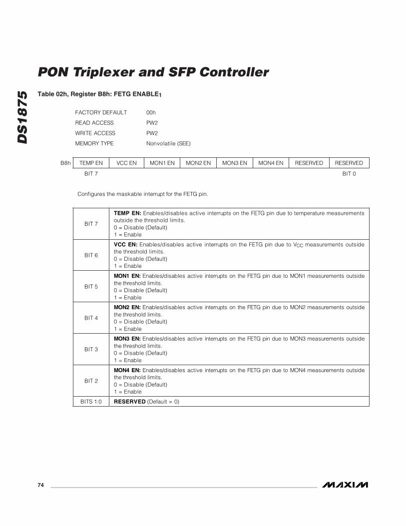
DS
18
75
PON Triplexer and SFP Controller
74 ______________________________________________________________________________________
Table 02h, Register B8h: FETG ENABLE1
FACTORY DEFAULT 00h
READ ACCESS PW2
WRITE ACCESS PW2
MEMORY TYPE Nonvolatile (SEE)
B8h TEMP EN VCC EN MON1 EN MON2 EN MON3 EN MON4 EN RESERVED RESERVED
BIT 7 BIT 0
Configures the maskable interrupt for the FETG pin.
BIT 7
TEMP EN: Enables/disables active interrupts on the FETG pin due to temperature measurements outside the threshold limits. 0 = Disable (Default) 1 = Enable
BIT 6
VCC EN: Enables/disables active interrupts on the FETG pin due to VCC measurements outside the threshold limits. 0 = Disable (Default) 1 = Enable
BIT 5
MON1 EN: Enables/disables active interrupts on the FETG pin due to MON1 measurements outside the threshold limits. 0 = Disable (Default) 1 = Enable
BIT 4
MON2 EN: Enables/disables active interrupts on the FETG pin due to MON2 measurements outside the threshold limits. 0 = Disable (Default) 1 = Enable
BIT 3
MON3 EN: Enables/disables active interrupts on the FETG pin due to MON3 measurements outside the threshold limits. 0 = Disable (Default) 1 = Enable
BIT 2
MON4 EN: Enables/disables active interrupts on the FETG pin due to MON4 measurements outside the threshold limits. 0 = Disable (Default) 1 = Enable
BITS 1:0 RESERVED (Default = 0)

DS
18
75
Table 02h, Register B9h: FETG ENABLE0
FACTORY DEFAULT 00h
READ ACCESS PW2
WRITE ACCESS PW2
MEMORY TYPE Nonvolatile (SEE)
B9h TXP HI EN TXP LO EN BIAS HI EN BIAS MAX
EN RESERVED RESERVED RESERVED RESERVED
BIT 7 BIT 0
Configures the maskable interrupt for the FETG pin.
BIT 7
TXP HI EN: Enables/disables active interrupts on the FETG pin due to TXP fast comparisons above the threshold limit. 0 = Disable (Default) 1 = Enable
BIT 6
TXP LO EN: Enables/disables active interrupts on the FETG pin due to TXP fast comparisons below the threshold limit. 0 = Disable (Default) 1 = Enable
BIT 5
BIAS HI EN: Enables/disables active interrupts on the FETG pin due to BIAS fast comparisons above the threshold limit. 0 = Disable. (Default) 1 = Enable
BIT 4
BIAS MAX EN: Enables/disables active interrupts on the FETG pin due to BIAS fast comparisons below the threshold limit. 0 = Disable (Default) 1 = Enable
BITS 3:0 RESERVED (Default = 0)
PON Triplexer and SFP Controller
______________________________________________________________________________________ 75

DS
18
75
PON Triplexer and SFP Controller
76 ______________________________________________________________________________________
Table 02h, Register BAh: TX-F ENABLE1
FACTORY DEFAULT 00h
READ ACCESS PW2
WRITE ACCESS PW2
MEMORY TYPE Nonvolatile (SEE)
BAh TEMP EN VCC EN MON1 EN MON2 EN MON3 EN MON4 EN RESERVED RESERVED
BIT 7 BIT 0
Configures the maskable interrupt for the TX-F pin.
BIT 7
TEMP EN: Enables/disables active interrupts on the TX-F pin due to temperature measurements outside the threshold limits. 0 = Disable (Default) 1 = Enable
BIT 6
VCC EN: Enables/disables active interrupts on the TX-F pin due to VCC measurements outside the threshold limits. 0 = Disable (Default) 1 = Enable
BIT 5
MON1 EN: Enables/disables active interrupts on the TX-F pin due to MON1 measurements outside the threshold limits. 0 = Disable (Default) 1 = Enable
BIT 4
MON2 EN: Enables/disables active interrupts on the TX-F pin due to MON2 measurements outside the threshold limits. 0 = Disable (Default) 1 = Enable
BIT 3
MON3 EN: Enables/disables active interrupts on the TX-F pin due to MON3 measurements outside the threshold limits. 0 = Disable (Default) 1 = Enable
BIT 2
MON4 EN: Enables/disables active interrupts on the TX-F pin due to MON4 measurements outside the threshold limits. 0 = Disable (Default) 1 = Enable
BITS 2:0 RESERVED (Default = 0)

DS
18
75
Table 02h, Register BBh: TX-F ENABLE0
FACTORY DEFAULT 00h
READ ACCESS PW2
WRITE ACCESS PW2
MEMORY TYPE Nonvolatile (SEE)
BBh TXP HI EN TXP LO EN BIAS HI EN BIAS MAX
EN RESERVED RESERVED RESERVED FETG EN
BIT 7 BIT 0
Configures the maskable interrupt for the TX-F pin.
BIT 7
TXP HI EN: Enables/disables active interrupts on the TX-F pin due to TXP fast comparisons above the threshold limit. 0 = Disable (Default) 1 = Enable
BIT 6
TXP LO EN: Enables/disables active interrupts on the TX-F pin due to TXP fast comparisons below the threshold limit. 0 = Disable (Default) 1 = Enable
BIT 5
BIAS HI EN: Enables/disables active interrupts on the TX-F pin due to BIAS fast comparisons above the threshold limit. 0 = Disable (Default) 1 = Enable
BIT 4
BIAS MAX EN: Enables/disables active interrupts on the TX-F pin due to BIAS fast comparisons above the threshold limit. 0 = Disable (Default) 1 = Enable
BITS 3:1 RESERVED (Default = 0)
BIT 0 FETG EN: 0 = Normal FETG operation (Default). 1 = Enables FETG to act as an input to TX-F output.
PON Triplexer and SFP Controller
______________________________________________________________________________________ 77

DS
18
75
PON Triplexer and SFP Controller
78 ______________________________________________________________________________________
Table 02h, Register BCh: HTXP
FACTORY DEFAULT 00h
READ ACCESS PW2
WRITE ACCESS PW2
MEMORY TYPE Nonvolatile (SEE)
BCh 27 26 25 24 23 22 21 20
BIT 7 BIT 0
Fast comparison DAC threshold adjust for high TXP. This value is added to the APC DAC value recalled from Table 04h. If the sum is greater than 0xFF, 0xFF is used. Comparisons greater than VHTXP, compared against VBMD, create a TXP HI alarm. The same ranging applied to the APC DAC should be used here.
VHTXP =Full Scale
255HTXP + APC DAC( )
Table 02h, Register BDh: LTXP
FACTORY DEFAULT 00h
READ ACCESS PW2
WRITE ACCESS PW2
MEMORY TYPE Nonvolatile (SEE)
BDh 27 26 25 24 23 22 21 20
BIT 7 BIT 0
Fast-comparison DAC threshold adjust for low TXP. This value is subtracted from the APC DAC value recalled from Table 04h. If the difference is less than 0x00, 0x00 is used. Comparisons less than VLTXP, compared against VBMD, create a TXP LO alarm. The same ranging applied to the APC DAC should be used here.
VLTXP =Full Scale
255APC DAC LTXP( )

DS
18
75
Table 02h, Register BEh: HBIAS
FACTORY DEFAULT 00h
READ ACCESS PW2
WRITE ACCESS PW2
MEMORY TYPE Nonvolatile (SEE)
BEh 27 26 25 24 23 22 21 20
BIT 7 BIT 0
Fast-comparison DAC setting for high BIAS. Comparisons greater than VHBIAS, found on the MON1 pin, create a BIAS HI alarm.
VHBIAS =Full Scale
255HBIAS
Table 02h, Register BFh: MAX BIAS
FACTORY DEFAULT 00h
READ ACCESS PW2
WRITE ACCESS PW2
MEMORY TYPE Nonvolatile (SEE)
BFh 212 211 210 29 28 27 26 25
BIT 7 BIT 0
This value defines the maximum DAC value allowed for the upper 8 bits of BIAS output during all operations.
PON Triplexer and SFP Controller
______________________________________________________________________________________ 79
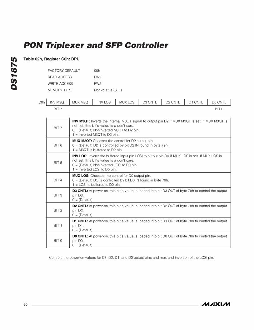
DS
18
75
PON Triplexer and SFP Controller
80 ______________________________________________________________________________________
Table 02h, Register C0h: DPU
FACTORY DEFAULT 00h
READ ACCESS PW2
WRITE ACCESS PW2
MEMORY TYPE Nonvolatile (SEE)
C0h INV M3QT MUX M3QT INV LOS MUX LOS D3 CNTL D2 CNTL D1 CNTL D0 CNTL
BIT 7 BIT 0
BIT 7
INV M3QT: Inverts the internal M3QT signal to output pin D2 if MUX M3QT is set. If MUX M3QT is not set, this bit’s value is a don’t care.0 = (Default) Noninverted M3QT to D2 pin. 1 = Inverted M3QT to D2 pin.
BIT 6 MUX M3QT: Chooses the control for D2 output pin.0 = (Default) D2 is controlled by bit D2 IN found in byte 79h. 1 = M3QT is buffered to D2 pin.
BIT 5
INV LOS: Inverts the buffered input pin LOSI to output pin D0 if MUX LOS is set. If MUX LOS is not set, this bit’s value is a don’t care.0 = (Default) Noninverted LOSI to D0 pin. 1 = Inverted LOSI to D0 pin.
BIT 4 MUX LOS: Chooses the control for D0 output pin.0 = (Default) DO is controlled by bit D0 IN found in byte 79h. 1 = LOSI is buffered to D0 pin.
BIT 3 D3 CNTL: At power-on, this bit’s value is loaded into bit D3 OUT of byte 78h to control the output pin D3. 0 = (Default)
BIT 2 D2 CNTL: At power-on, this bit’s value is loaded into bit D2 OUT of byte 78h to control the output pin D2. 0 = (Default)
BIT 1 D1 CNTL: At power-on, this bit’s value is loaded into bit D1 OUT of byte 78h to control the output pin D1. 0 = (Default)
BIT 0 D0 CNTL: At power-on, this bit’s value is loaded into bit D0 OUT of byte 78h to control the output pin D0. 0 = (Default)
Controls the power-on values for D3, D2, D1, and D0 output pins and mux and invertion of the LOSI pin.

DS
18
75
Table 02h, Register C1h to C2h: RESERVED
FACTORY DEFAULT 00h
READ ACCESS PW2
WRITE ACCESS PW2
MEMORY TYPE Nonvolatile (SEE)
These registers are reserved.
Table 02h, Register C3h: M3QT DAC
FACTORY DEFAULT 00h
READ ACCESS PW2
WRITE ACCESS PW2
MEMORY TYPE Nonvolatile (SEE)
C3h 27 26 25 24 23 22 21 20
BIT 7 BIT 0
Register to control M3QT DAC.
VM3QT =1.25256
M3QT DAC +1( )
Table 02h, Register C4h: DAC1
FACTORY DEFAULT 00h
READ ACCESS PW2
WRITE ACCESS PW2
MEMORY TYPE Nonvolatile (SEE)
C4h 27 26 25 24 23 22 21 20
BIT 7 BIT 0
Register to control DAC1.
VDACI =2.5256
DAC1+1( )
PON Triplexer and SFP Controller
______________________________________________________________________________________ 81

DS
18
75
PON Triplexer and SFP Controller
82 ______________________________________________________________________________________
Table 02h, Register C5h to C6h: RESERVED
FACTORY DEFAULT 00h
READ ACCESS PW2
WRITE ACCESS PW2
MEMORY TYPE Nonvolatile (SEE)
These registers are reserved.
Table 02h, Register C7h: M4 LUT CNTL
FACTORY DEFAULT 00h
READ ACCESS PW2
WRITE ACCESS PW2
MEMORY TYPE Nonvolatile (SEE)
C7h RESERVED RESERVED RESERVED RESERVED FBOL FBCL DBL_SB UP_LOWB
BIT 7 BIT 0
BITS 7:4 RESERVED (Default = 000000b)
BITS 3:2
FBOL and FBCL: Force bias open loop and force bias closed loop. 00b = (Default) normal operation. 10b = Force control of IBIAS to be open loop regardless of duration of BEN pulses. 01b = Force control of IBIAS to be closed loop regardless of duration of BEN pulses. 11b = Same as 10b. When forcing open-loop mode, BEN should be ground or at any burst length.
BIT 1 DBL_SB: Chooses the size of LUT for Table 06h. 0 = (Default) Single LUT of 32 bytes. 1 = Double LUT of 16 bytes.
BIT 0
UP_LOWB: Determines which 16-byte LUT is used if DBL_SB = 1. If DBL_SB = 0, the value of this bit is a don’t care. 0 = (Default) Chooses the lower 16 bytes of Table 06h (80h to 8Fh). 1 = Chooses the upper 16 bytes of Table 06h (90h to 9Fh).
Controls the size and location of LUT functions for the MON4 measurement.

DS
18
75
Table 02h, Register C8h to C9h: MON5 SCALETable 02h, Register CAh to CBh: MON6 SCALETable 02h, Register CCh to CDh: MON7 SCALETable 02h, Register CEh to CFh: MON8 SCALE
FACTORY CALIBRATED
READ ACCESS PW2
WRITE ACCESS PW2
MEMORY TYPE Nonvolatile (SEE)
C8h, CAh, CCh, CEh
215 214 213 212 211 210 29 28
C9h, CBh, CDh, CFh
27 26 25 24 23 22 21 20
BIT 7 BIT 0
Controls the scaling or gain of the FS voltage measurements. The factory-calibrated value produces an FS voltage of 2.5V for MON5, MON6, MON7, and MON8.
Table 02h, Register D0h to D1h: MON5 OFFSETTable 02h, Register D2h to D3h: MON6 OFFSETTable 02h, Register D4h to D5h: MON7 OFFSETTable 02h, Register D6h to D7h: MON8 OFFSET
FACTORY DEFAULT 00h
READ ACCESS PW2
WRITE ACCESS PW2
MEMORY TYPE Nonvolatile (SEE)
D0h, D2h, D4h, D6h
S S 215 214 213 212 211 210
D1h, D3h, D5h, D7h
29 28 27 26 25 24 23 22
BIT 7 BIT 0
Allows for offset control of these voltage measurements if desired.
PON Triplexer and SFP Controller
______________________________________________________________________________________ 83

DS
18
75
PON Triplexer and SFP Controller
84 ______________________________________________________________________________________
Table 02h, Register D8h to F7h: EMPTYTable 02h, Register F8h to F9h: MAN BIAS
FACTORY DEFAULT 00h
READ ACCESS PW2
WRITE ACCESS PW2 and BIAS EN = 1
MEMORY TYPE Volatile
FAh RESERVED RESERVED RESERVED RESERVED RESERVED RESERVED RESERVED MAN_CLK
BIT 7 BIT 0
When BIAS EN (Table 02h, Register 80h) is written to 0, bit 0 of this byte controls the updates of the MAN BIAS value to the BIAS output. The values of MAN BIAS should be written with a separate write command. Setting bit 0 to a 1 clocks the MAN BIAS value to the output DAC.
1. Write the MAN BIAS value with a write command. 2. Set the MAN_CLK bit to a 1 with a separate write command. 3. Clear the MAN_CLK bit to a 0 with a separate write command.
Table 02h, Register FAh: MAN_CNTL
FACTORY DEFAULT 00h
READ ACCESS PW2
WRITE ACCESS PW2 and BIAS EN = 1
MEMORY TYPE Volatile
F8h RESERVED RESERVED 212 211 210 29 28 27
F9h 27 26 25 24 23 22 21 20
BIT 7 BIT 0
When BIAS EN (Table 02h, Register 80h) is written to 0, writes to these bytes control the BIAS DAC.
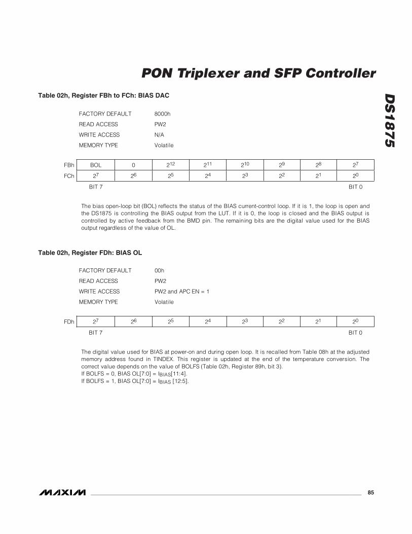
DS
18
75
Table 02h, Register FBh to FCh: BIAS DAC
FACTORY DEFAULT 8000h
READ ACCESS PW2
WRITE ACCESS N/A
MEMORY TYPE Volatile
FBh BOL 0 212 211 210 29 28 27
FCh 27 26 25 24 23 22 21 20
BIT 7 BIT 0
The bias open-loop bit (BOL) reflects the status of the BIAS current-control loop. If it is 1, the loop is open and the DS1875 is controlling the BIAS output from the LUT. If it is 0, the loop is closed and the BIAS output is controlled by active feedback from the BMD pin. The remaining bits are the digital value used for the BIAS output regardless of the value of OL.
Table 02h, Register FDh: BIAS OL
FACTORY DEFAULT 00h
READ ACCESS PW2
WRITE ACCESS PW2 and APC EN = 1
MEMORY TYPE Volatile
FDh 27 26 25 24 23 22 21 20
BIT 7 BIT 0
The digital value used for BIAS at power-on and during open loop. It is recalled from Table 08h at the adjusted memory address found in TINDEX. This register is updated at the end of the temperature conversion. The correct value depends on the value of BOLFS (Table 02h, Register 89h, bit 3). If BOLFS = 0, BIAS OL[7:0] = IBIAS[11:4]. If BOLFS = 1, BIAS OL[7:0] = IBIAS [12:5].
PON Triplexer and SFP Controller
______________________________________________________________________________________ 85

DS
18
75
PON Triplexer and SFP Controller
86 ______________________________________________________________________________________
Table 02h, Register FEh: PWM DAC
FACTORY DEFAULT 00h
READ ACCESS PW2
WRITE ACCESS PW2 and PWM EN = 0
MEMORY TYPE Volatile
FEh 27 26 25 24 23 22 21 20
BIT 7 BIT 0
The digital value used for PWM integration of the FB pin. It is recalled from Table 07h at the adjusted memory address found in TINDEX. This register is updated at the end of the temperature conversion.
VPWM =1.25256
(PWM DAC +1)
Table 02h, Register FFh: RESERVED
FACTORY DEFAULT 00h
READ ACCESS PW2
WRITE ACCESS N/A
MEMORY TYPE N/A
This register is reserved.

DS
18
75
Table 03h Register DescriptionsTable 03h, Register 80h to FFh: PW2 EEPROM
FACTORY DEFAULT 00h
READ ACCESS PW2
WRITE ACCESS PW2
MEMORY TYPE Nonvolatile (EE)
80h to FFh EE EE EE EE EE EE EE EE
BIT 7 BIT 0
PW2-protected EEPROM.
Table 04h Register DescriptionsTable 04h, Register 80h to C7h: MODULATION LUT
FACTORY DEFAULT 00h
READ ACCESS PW2
WRITE ACCESS PW2
MEMORY TYPE Nonvolatile (EE)
80h to C7h 27 26 25 24 23 22 21 20
BIT 7 BIT 0
The digital value for the modulation DAC output. The MODULATION LUT is a set of registers assigned to hold the temperature profile for the modulation DAC. The values in this table combined with the MOD bits in the MOD RANGING register (Table 02h, Register 8Bh) determine the set point for the modulation voltage. The temperature measurement is used to index the LUT (TINDEX, Table 02h, Register 81h) in 2°C increments from -40°C to +102°C, starting at 80h in Table 04h. Register 80h defines the -40°C to -38°C MOD output, Register 81h defines the -38°C to -36°C MOD output, and so on. Values recalled from this EEPROM memory table are written into the MOD DAC (Table 02h, Register 82h) location that holds the value until the next temperature conversion. The DS1875 can be placed into a manual mode (MOD EN bit, Table 02h, Register 80h), where MOD DAC is directly controlled for calibration. If the temperature compensation functionality is not required, then program the entire Table 04h, to the desired modulation setting.
PON Triplexer and SFP Controller
______________________________________________________________________________________ 87

DS
18
75
PON Triplexer and SFP Controller
88 ______________________________________________________________________________________
Table 05h Register DescriptionsTable 05h, Register 80h to A3h: APC TE LUT
FACTORY DEFAULT 00h
READ ACCESS PW2
WRITE ACCESS PW2
MEMORY TYPE Nonvolatile (EE)
80h to A3h 27 26 25 24 23 22 21 20
BIT 7 BIT 0
The APC TE LUT is a set of registers assigned to hold the temperature profile for the APC reference DAC. The values in this table combined with the APC bits in the COMP RANGING register (Table 02h, Register 8Dh) determine the set point for the APC loop. The temperature measurement is used to index the LUT (TINDEX, Table 02h, Register 81h) in 4°C increments from -40°C to +100°C, starting at Register 80h in Table 05h. Register 80h defines the -40°C to -36°C APC reference value, Register 81h defines the -36°C to -32°C APC reference value, and so on. Values recalled from this EEPROM memory table are written into the APC DAC (Table 02h, Register 83h) location that holds the value until the next temperature conversion. The DS1875 can be placed into a manual mode (APC EN bit, Table 02h, Register 80h), where APC DAC can be directly controlled for calibration. If TE temperature compensation is not required by the application, program the entire LUT to the desired APC set point.
Table 05h, Register A4h to A7h: RESERVED
FACTORY DEFAULT 00h
READ ACCESS PW2
WRITE ACCESS PW2
MEMORY TYPE Nonvolatile (EE)
These registers are reserved.
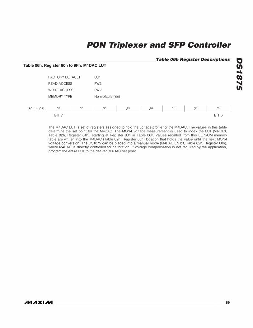
DS
18
75
Table 06h Register DescriptionsTable 06h, Register 80h to 9Fh: M4DAC LUT
FACTORY DEFAULT 00h
READ ACCESS PW2
WRITE ACCESS PW2
MEMORY TYPE Nonvolatile (EE)
80h to 9Fh 27 26 25 24 23 22 21 20
BIT 7 BIT 0
The M4DAC LUT is set of registers assigned to hold the voltage profile for the M4DAC. The values in this table determine the set point for the M4DAC. The MON4 voltage measurement is used to index the LUT (VINDEX, Table 02h, Register 84h), starting at Register 80h in Table 06h. Values recalled from this EEPROM memory table are written into the M4DAC (Table 02h, Register 85h) location that holds the value until the next MON4 voltage conversion. The DS1875 can be placed into a manual mode (M4DAC EN bit, Table 02h, Register 80h), where M4DAC is directly controlled for calibration. If voltage compensation is not required by the application, program the entire LUT to the desired M4DAC set point.
PON Triplexer and SFP Controller
______________________________________________________________________________________ 89

DS
18
75
PON Triplexer and SFP Controller
90 ______________________________________________________________________________________
Table 07h Register DescriptionsTable 07h, Register 80h to A3h: PWM REFERENCE LUT
FACTORY DEFAULT 00h
READ ACCESS PW2
WRITE ACCESS PW2
MEMORY TYPE Nonvolatile (EE)
80h to A3h 27 26 25 24 23 22 21 20
BIT 7 BIT 0
The PWM REFERENCE LUT is a set of registers assigned to hold the temperature profile for the PWM feedback. The values in this table determine the set point for the PWM loop. The temperature measurement is used to index the LUT (TINDEX, Table 02h, Register 81h) in 4°C increments from -40°C to +100°C, starting at Register 80h in Table 07h. Register 80h defines the -40°C to -36°C PWM reference value, Register 81h defines the -36°C to -32°C PWM reference value, and so on. Values recalled from this EEPROM memory table are written into the PWM DAC (Table 02h, Register FEh) location that holds the value until the next temperature conversion. The DS1875 can be placed into a manual mode (PWM EN bit, Table 02h, Register 80h), where PWM DAC can be directly controlled for calibration. If temperature compensation is not required by the application, program the entire LUT to the desired PWM set point.
Table 07h, Register A4h to A7h: RESERVED
FACTORY DEFAULT 00h
READ ACCESS PW2
WRITE ACCESS PW2
MEMORY TYPE Nonvolatile (SEE)
These registers are reserved.

DS
18
75
PON Triplexer and SFP Controller
______________________________________________________________________________________ 91
FACTORY DEFAULT 00h
READ ACCESS All
WRITE ACCESS All
MEMORY TYPE Nonvolatile (EE)
80h to C7h 27 26 25 24 23 22 21 20
BIT 7 BIT 0
The BIAS OPEN-LOOP LUT is a set of registers assigned to hold the temperature profile for the BIAS OL DAC. The values in this table determine the set point for the BIAS current. The temperature measurement is used to index the LUT (TINDEX, Table 02h, Register 81h) in 2°C increments from -40°C to +102°C, starting at 80h in Table 08h. Register 80h defines the -40°C to -38°C BIAS OL output, Register 81h defines the -38°C to -36°C BIAS OL output, and so on. Values recalled from this EEPROM memory table are written into the BIAS OL (Table 02h, Register FDh) location that holds the value until the next temperature conversion. The DS1875 can be placed into a manual mode (BIAS EN bit, Table 02h, Register 80h), where BIAS OL DAC is directly controlled for calibration. If the temperature compensation functionality is not required, then program the entire Table 08h to the desired BIAS OL setting.
Auxiliary Memory A0h Register DescriptionsAuxiliary Memory A0h, Register 00h to FFh: EEPROM
FACTORY DEFAULT 00h
READ ACCESS ALL
WRITE ACCESS ALL
MEMORY TYPE Nonvolatile (EE)
80h to FFh 27 26 25 24 23 22 21 20
BIT 7 BIT 0
Accessible with the slave address A0h.
PACKAGE TYPE PACKAGE CODE DOCUMENT NO.
38 TQFN-EP T3857+1 21-0172
Package InformationFor the latest package outline information and land patterns, go to www.maxim-ic.com/packages.
Table 08h Register DescriptionsTable 08h, Register 80h to C7h: BIAS OPEN-LOOP LUT
DS
18
75
PON Triplexer and SFP Controller
Maxim cannot assume responsibility for use of any circuitry other than circuitry entirely embodied in a Maxim product. No circuit patent licenses areimplied. Maxim reserves the right to change the circuitry and specifications without notice at any time.
92 ____________________Maxim Integrated Products, 120 San Gabriel Drive, Sunnyvale, CA 94086 408-737-7600
© 2008 Maxim Integrated Products is a registered trademark of Maxim Integrated Products, Inc.
Revision HistoryREVISION NUMBER
REVISION DATE
DESCRIPTION PAGES
CHANGED
0 7/08 Initial release. —
1 10/08 Updated all instances of the operating voltage range from 5.5V to 3.9V on multiple pages.
1, 5–13