SFP-DD Rev 1.0 SFP-DD MSAsfp-dd.com/wp-content/uploads/2017/09/SFP-DDrev1-0-9-14-17.pdf · SFP-DD...
50
SFP-DD Rev 1.0 1 SFP-DD MSA SFP-DD Hardware Specification for SFP DOUBLE DENSITY 2X PLUGGABLE TRANSCEIVER Rev 1.0 September 14, 2017 Abstract: This specification defines: the electrical and optical connectors, electrical signals and power supplies, mechanical and thermal requirements of the pluggable SFP Double Density (SFP-DD) module, connector and cage system. This document provides a common specification for systems manufacturers, system integrators, and suppliers of modules. POINTS OF CONTACT: Tom Palkert Scott Sommers Technical Editor Chair Molex Molex 2222 Wellington Court 2222 Wellington Court Lisle, IL 60532-1682 Lisle, IL 60532-1682 Ph: 952-200-8542 Ph: 630-527-4317 tom.palkert at molex.com scott.sommers at molex.com www.SFP-dd.com Limitation on use of Information: This specification is provided "AS IS" with NO WARRANTIES whatsoever and therefore the provision of this specification does not include any warranty of merchantability, noninfringement, fitness for a particular purpose, or any other warranty otherwise arising out of any proposal, specification or sample. The authors further disclaim all liability, including liability for infringement of any proprietary rights, relating to use of information in this specification. No license, express or implied, by estoppel or otherwise, to any intellectual property rights is granted herein. Permissions: You are authorized to download, reproduce and distribute this document. All other rights are reserved. The provision of this document should not be construed as the granting of any right to practice, make, use or otherwise develop products that are based on the document. Any and all IP rights related to this document and the designs disclosed within, except for the rights expressly mentioned above, are reserved by the respective owners of those IP rights.
Transcript of SFP-DD Rev 1.0 SFP-DD MSAsfp-dd.com/wp-content/uploads/2017/09/SFP-DDrev1-0-9-14-17.pdf · SFP-DD...
SFP-DD Rev 1.0
1
SFP-DD MSA
SFP-DD Hardware Specification
for
SFP DOUBLE DENSITY 2X PLUGGABLE TRANSCEIVER
Rev 1.0 September 14, 2017 Abstract: This specification defines: the electrical and optical connectors, electrical signals and power supplies, mechanical and thermal requirements of the pluggable SFP Double Density (SFP-DD) module, connector and cage system. This document provides a common specification for systems manufacturers, system integrators, and suppliers of modules. POINTS OF CONTACT: Tom Palkert Scott Sommers Technical Editor Chair Molex Molex 2222 Wellington Court 2222 Wellington Court Lisle, IL 60532-1682 Lisle, IL 60532-1682 Ph: 952-200-8542 Ph: 630-527-4317 tom.palkert at molex.com scott.sommers at molex.com www.SFP-dd.com Limitation on use of Information: This specification is provided "AS IS" with NO WARRANTIES whatsoever and therefore the provision of this specification does not include any warranty of merchantability, noninfringement, fitness for a particular purpose, or any other warranty otherwise arising out of any proposal, specification or sample. The authors further disclaim all liability, including liability for infringement of any proprietary rights, relating to use of information in this specification. No license, express or implied, by estoppel or otherwise, to any intellectual property rights is granted herein. Permissions: You are authorized to download, reproduce and distribute this document. All other rights are reserved. The provision of this document should not be construed as the granting of any right to practice, make, use or otherwise develop products that are based on the document. Any and all IP rights related to this document and the designs disclosed within, except for the rights expressly mentioned above, are reserved by the respective owners of those IP rights.
SFP-DD Rev 1.0
2
The following are Promoter member companies of the SFP-DD MSA. Alibaba Group Broadcom Brocade Cisco Dell/EMC Finisar Hewlett Packard Enterprise Huawei Intel Juniper Networks Lumentum Mellanox Technologies Molex TE Connectivity Change History: Revision Date Changes 1.0 September 14 2017 First public release Foreword The development work on this specification was done by the SFP-DD MSA, an industry group. The membership of the committee since its formation in May 2017 has included a mix of companies which are leaders across the industry. TABLE OF CONTENTS
1. Scope.............................................................................. 6
1.1 Description of Sections .......................................................................................................................................... 6
2. References......................................................................... 6
2.1 Industry Documents ...................................................................................................................................................... 6
2.2 Sources ................................................................................................................................................................................ 7
3 Introduction......................................................................... 7
3.1 Objectives ......................................................................................................................................................................... 7
3.2 Applications .................................................................................................................................................................... 8
4 Electrical Specification.............................................................. 9
4.1 Electrical Connector ...................................................................................................................................................... 9 4.1.1 Low Speed Electrical Hardware Signals ................................................................................................... 16 4.1.2 Low Speed Electrical Specification .......................................................................................................... 17 4.1.3 2 Wire Management Interface Specification ......................................................................................... 17 4.1.4 High Speed Electrical Specification ........................................................................................................ 18
SFP-DD Rev 1.0
3
4.2 Rate Select Hardware Control ................................................................................................................................. 19
4.3 Power Requirements ......................................................................................................................................................... 19 4.3.1 Power Classes and Maximum Power Consumption ..................................................................................... 20 4.3.2 Host Board Power Supply Filtering ............................................................................................................ 20 4.3.3 Module Power Supply Specification ............................................................................................................ 21 4.3.4 Host Board Power Supply Noise Output ..................................................................................................... 23 4.3.5 Module Power Supply Noise Output ............................................................................................................... 23 4.3.6 Module Power Supply Noise Tolerance ........................................................................................................ 23
4.4 ESD ............................................................................................................................................................................................. 23
5 Mechanical and Board Definition...................................................... 24
5.1 Introduction ....................................................................................................................................................................... 24
5.2 Cage, Connector, Module Alignment ..................................................................................................................... 25
5.3 Module Mechanical Dimensions ................................................................................................................................. 26
5.4 Module Flatness and Roughness ............................................................................................................................... 30
5.5 Module paddle card dimensions ............................................................................................................................ 31
5.6 Module Extraction and Retention Forces ......................................................................................................... 34
5.7 Press fit Cage Mechanical ........................................................................................................................................ 35
5.8 SMT Electrical Connector Mechanical ................................................................................................................ 39 5.8.1 SMT connector and cage host PCB layout................................................................................................. 43
5.9 Module Color Coding and Labeling ........................................................................................................................ 45
5.10 Optical Interface ......................................................................................................................................................... 45 5.10.1 MPO Optical Cable connections .................................................................................................................... 46 5.10.2 Dual LC Optical Cable connection ............................................................................................................ 46 5.10.3 Electrical data input/output to optical port mapping .......................................................... 47
6 Environmental and Thermal............................................................ 47
6.1 Thermal Requirements .................................................................................................................................................... 47
7 Management Interface Timing.......................................................... 47
7.1 SCL and SDA Timing Specification ........................................................................................................................ 48 7.1.1 Introduction .............................................................................................................................................................. 48 7.1.2 Management Interface Timing Specification ......................................................................................... 48
7.2 Serial Interface Protocol ........................................................................................................................................ 48 7.2.1 Management Timing Parameters ........................................................................................................................ 48
7.3 Timing for Soft Control and Status Functions ........................................................................................... 50
SFP-DD Rev 1.0
4
Table 1- Pad Function Definition....................................................... 11 Table 2: Low Speed Control and Sense Signals........................................... 18 Table 3: Rate Select Hardware Control.................................................. 19 Table 4- Power Classification.......................................................... 20 Table 5- Power Supply specifications, Instantaneous, sustained and steady state current limits................................................................................. 22 Table 6- Module flatness specifications................................................ 30 Table 7- Insertion, Extraction and Retention Forces.................................... 34 Table 8- Electrical data input to Optical Port Mapping................................. 47 Table 9- Temperature Range Class of operation.......................................... 47 Table 10- Management Interface timing parameters....................................... 49 Table 11- Timing for SFP-DD soft control and status functions.......................... 50
SFP-DD Rev 1.0
5
Figure 1: Application Reference Model................................................... 8 Figure 2: SFP-DD Cage, Connector and Module............................................. 8 Figure 3: Module pad layout............................................................ 10 Figure 4: Example SFP-DD Host Board Schematic For Optical Modules...................... 13 Figure 5: Example SFP-DD Host Board Schematic for active copper cables................. 14 Figure 6: Example SFP-DD Host Board Schematic for passive copper cables................ 15 Figure 7: Recommended Host Board Power Supply Filtering................................ 20 Figure 8: Instantaneous and sustained peak currents for Icc Host (see Fig. 6).......... 23 Figure 9: Press fit cage............................................................... 24 Figure 10: Module...................................................................... 24 Figure 11: Cage, Connector alignment................................................... 25 Figure 12: Module...................................................................... 26 Figure 13: Detailed dimensions of module............................................... 29 Figure 14: Module paddle card dimensions............................................... 32 Figure 15: Module pad dimensions....................................................... 33 Figure 16: Press Fit 1x1 Cage.......................................................... 35 Figure 17: Press Fit 1x1 Cage Design................................................... 37 Figure 18: 1 x n bezel opening......................................................... 38 Figure 19: SMT connector............................................................... 40 Figure 20: 1x1 Connector Design and Host PCB Pin Numbers............................... 42 Figure 21: Host PCB Mechanical Layout.................................................. 44 Figure 22: Optical Media Dependent Interface port assignments.......................... 45 Figure 23: MPO-12 Single Row optical patch cord and module receptacle.................. 46 Figure 24: Dual LC optical patchcord and module receptacle............................. 47 Figure 25: SFP-DD Timing Diagram....................................................... 48 Figure 26: SDA/SCL options for pull-up resistor, bus capacitance and rise/fall times... 50
SFP-DD Rev 1.0
6
SFP-DD 2X Pluggable Transceiver
1. Scope The scope of this specification is the definition of a high density 2-channel module, cage and connector system. SFP-DD supports up to 100 Gb/s in aggregate over a 2 x 50Gb/s electrical interface. The cage and connector design provides backwards compatibility to SFP28 modules which can be inserted into a SFP-DD cage and connector using 1 of the electrical channels.
1.1 Description of Sections Section 1 Scope and Purpose Section 2 Referenced and Related Standards and SFF Specifications Section 3 Introduction Section 4 Electrical specifications Section 5 Mechanical specifications, printed circuit board recommendations, labeling, color code recommendations and optical interface examples. Section 6 Environmental and thermal considerations Section 7 Management Interface Timing
2. References
2.1 Industry Documents The following interface standards and specifications are relevant to this Specification. - GR-253-CORE - IEEE Std 802.3 - IEEE Std 802.3by - IEEE Std 802.3bs - IEEE Std 802.3cd - InfiniBand Architecture Specifications - FC-PI-7 - OIF CEI-56G-VSR-PAM4 - SFP-DD Management Interface SFF Specifications - INF-8436 SFP (Quad SFP) 4 Gbps 4X Transceiver - SFF-8636 Shielded Cables Common Management Interface - SFF-8472 Diagnostic Monitoring Interface for Optical Transceivers - SFF-8661 QSFP+ 4X Pluggable Module - SFF-8679 QSFP28 4X Base Electrical Specification - SFF-8402 SFP28 1x Pluggable Module - SFF-8071 SFP+ 1x0.8mm Card Edge Connector - SFF-8432 SFP+ Module and Cage
SFP-DD Rev 1.0
7
2.2 Sources This document can be obtained via the www.SFP-DD.com web site.
3 Introduction This Specification covers the following items: - Electrical interfaces including pad assignments for data, control, status and power supplies and host PCB layout requirements. - Optical interfaces (including optical receptacles and mating fiber plugs for multimode and single-mode duplex and parallel fiber applications). Breakout cable applications are also specified. - Mechanical specifications including dimensions and tolerances for the connector, cage and module system. Includes details of the requirements for correct mating of the module and host sides of the connector. - Thermal requirements - Electrostatic discharge (ESD) requirements by reference to industry standard limits and test methods. This Specification does not cover the following items: - Electromagnetic interference (EMI) protection. EMI protection is the responsibility of the implementers of the cages and modules. - Management Interface registers. - Optical signaling specifications are not included in this document but are defined in the applicable industry standards.
3.1 Objectives Electrical signal contact and channel assignments, electrical and power requirements defined in Section 4 and optical lane assignments defined in Section 5 ensure that the pluggable modules and cable assemblies are functionally interchangeable. Dimensions, mounting and insertion requirements defined in Section 5 for the bezel, optical module, cable plug, cage and connector system on a circuit board ensure that these products are mechanically interchangeable.
SFP-DD Rev 1.0
8
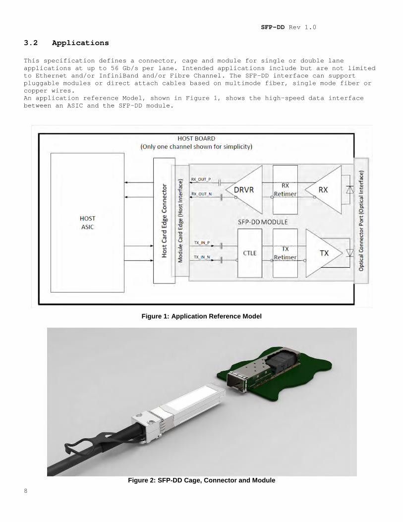
3.2 Applications This specification defines a connector, cage and module for single or double lane applications at up to 56 Gb/s per lane. Intended applications include but are not limited to Ethernet and/or InfiniBand and/or Fibre Channel. The SFP-DD interface can support pluggable modules or direct attach cables based on multimode fiber, single mode fiber or copper wires. An application reference Model, shown in Figure 1, shows the high-speed data interface between an ASIC and the SFP-DD module.
Figure 1: Application Reference Model
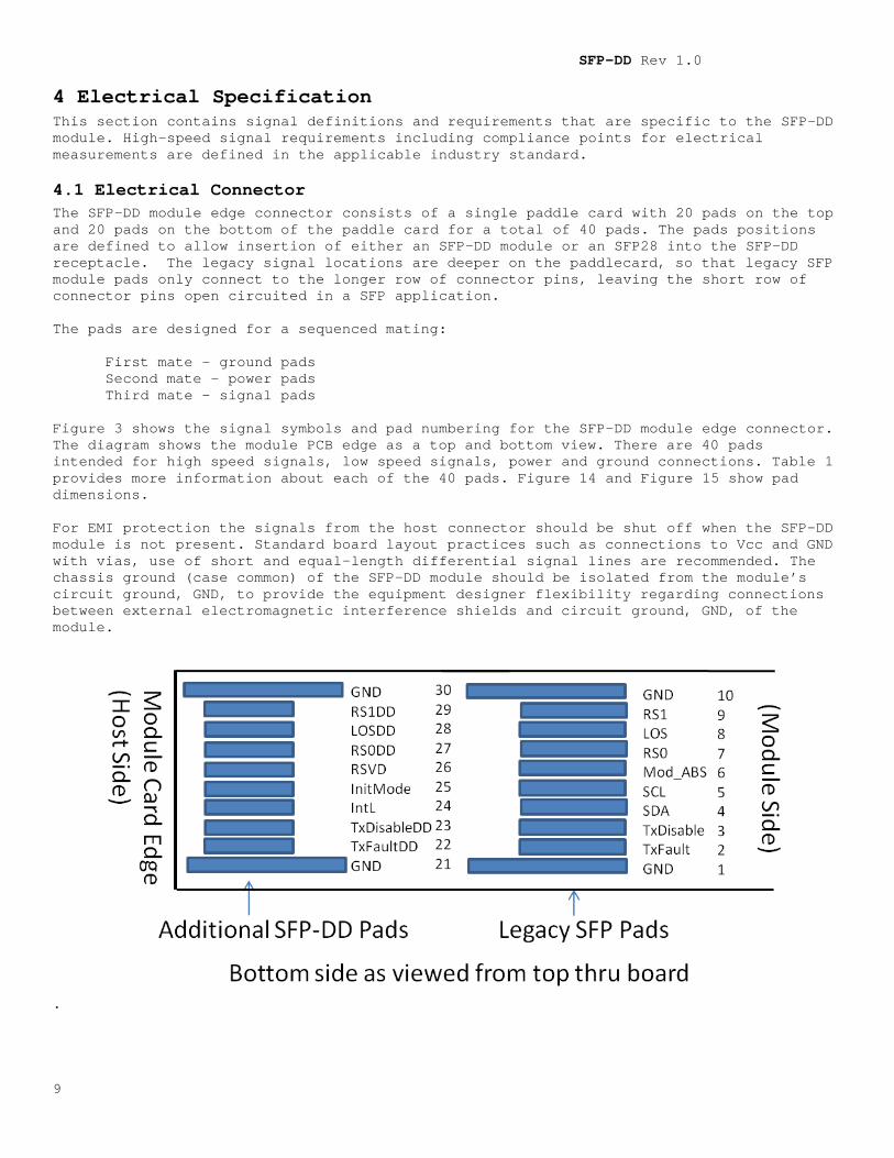
Figure 2: SFP-DD Cage, Connector and Module
SFP-DD Rev 1.0
9
4 Electrical Specification This section contains signal definitions and requirements that are specific to the SFP-DD module. High-speed signal requirements including compliance points for electrical measurements are defined in the applicable industry standard.
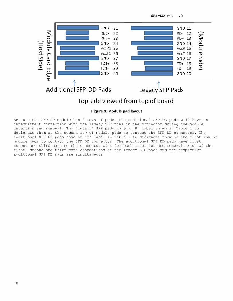
4.1 Electrical Connector The SFP-DD module edge connector consists of a single paddle card with 20 pads on the top and 20 pads on the bottom of the paddle card for a total of 40 pads. The pads positions are defined to allow insertion of either an SFP-DD module or an SFP28 into the SFP-DD receptacle. The legacy signal locations are deeper on the paddlecard, so that legacy SFP module pads only connect to the longer row of connector pins, leaving the short row of connector pins open circuited in a SFP application. The pads are designed for a sequenced mating:
First mate – ground pads Second mate – power pads Third mate – signal pads
Figure 3 shows the signal symbols and pad numbering for the SFP-DD module edge connector. The diagram shows the module PCB edge as a top and bottom view. There are 40 pads intended for high speed signals, low speed signals, power and ground connections. Table 1 provides more information about each of the 40 pads. Figure 14 and Figure 15 show pad dimensions. For EMI protection the signals from the host connector should be shut off when the SFP-DD module is not present. Standard board layout practices such as connections to Vcc and GND with vias, use of short and equal-length differential signal lines are recommended. The chassis ground (case common) of the SFP-DD module should be isolated from the module’s circuit ground, GND, to provide the equipment designer flexibility regarding connections between external electromagnetic interference shields and circuit ground, GND, of the module.
.
SFP-DD Rev 1.0
10
Figure 3: Module pad layout
Because the SFP-DD module has 2 rows of pads, the additional SFP-DD pads will have an intermittent connection with the legacy SFP pins in the connector during the module insertion and removal. The 'legacy' SFP pads have a 'B' label shown in Table 1 to designate them as the second row of module pads to contact the SFP-DD connector. The additional SFP-DD pads have an 'A' label in Table 1 to designate them as the first row of module pads to contact the SFP-DD connector. The additional SFP-DD pads have first, second and third mate to the connector pins for both insertion and removal. Each of the first, second and third mate connections of the legacy SFP pads and the respective additional SFP-DD pads are simultaneous.
SFP-DD Rev 1.0
11
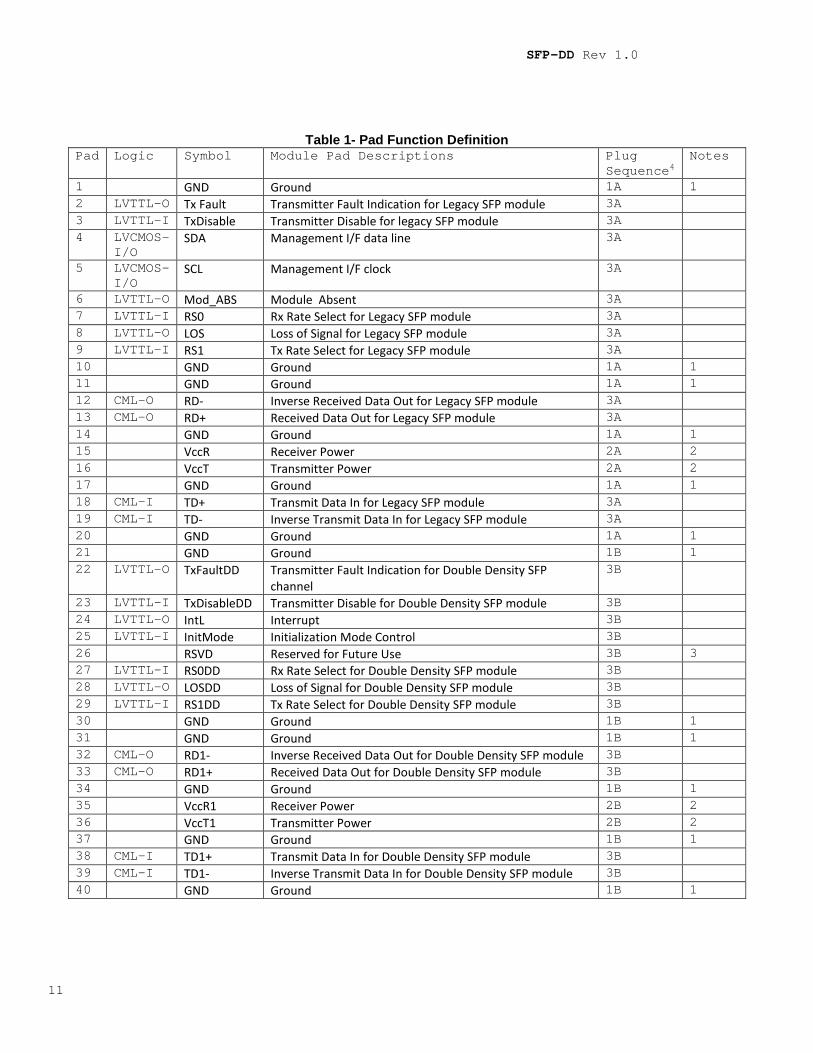
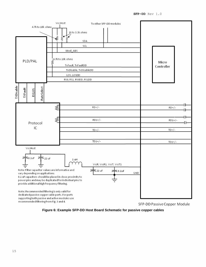
Table 1- Pad Function Definition Pad Logic Symbol Module Pad Descriptions Plug
Sequence4 Notes
1 GND Ground 1A 1 2 LVTTL-O Tx Fault Transmitter Fault Indication for Legacy SFP module 3A 3 LVTTL-I TxDisable Transmitter Disable for legacy SFP module 3A 4 LVCMOS-
I/O SDA Management I/F data line 3A
5 LVCMOS-I/O
SCL Management I/F clock 3A
6 LVTTL-O Mod_ABS Module Absent 3A 7 LVTTL-I RS0 Rx Rate Select for Legacy SFP module 3A 8 LVTTL-O LOS Loss of Signal for Legacy SFP module 3A 9 LVTTL-I RS1 Tx Rate Select for Legacy SFP module 3A 10 GND Ground 1A 1 11 GND Ground 1A 1 12 CML-O RD- Inverse Received Data Out for Legacy SFP module 3A 13 CML-O RD+ Received Data Out for Legacy SFP module 3A 14 GND Ground 1A 1 15 VccR Receiver Power 2A 2 16 VccT Transmitter Power 2A 2 17 GND Ground 1A 1 18 CML-I TD+ Transmit Data In for Legacy SFP module 3A 19 CML-I TD- Inverse Transmit Data In for Legacy SFP module 3A 20 GND Ground 1A 1 21 GND Ground 1B 1 22 LVTTL-O TxFaultDD Transmitter Fault Indication for Double Density SFP
channel 3B
23 LVTTL-I TxDisableDD Transmitter Disable for Double Density SFP module 3B 24 LVTTL-O IntL Interrupt 3B 25 LVTTL-I InitMode Initialization Mode Control 3B 26 RSVD Reserved for Future Use 3B 3 27 LVTTL-I RS0DD Rx Rate Select for Double Density SFP module 3B 28 LVTTL-O LOSDD Loss of Signal for Double Density SFP module 3B 29 LVTTL-I RS1DD Tx Rate Select for Double Density SFP module 3B 30 GND Ground 1B 1 31 GND Ground 1B 1 32 CML-O RD1- Inverse Received Data Out for Double Density SFP module 3B 33 CML-O RD1+ Received Data Out for Double Density SFP module 3B 34 GND Ground 1B 1 35 VccR1 Receiver Power 2B 2 36 VccT1 Transmitter Power 2B 2 37 GND Ground 1B 1 38 CML-I TD1+ Transmit Data In for Double Density SFP module 3B 39 CML-I TD1- Inverse Transmit Data In for Double Density SFP module 3B 40 GND Ground 1B 1
SFP-DD Rev 1.0
12
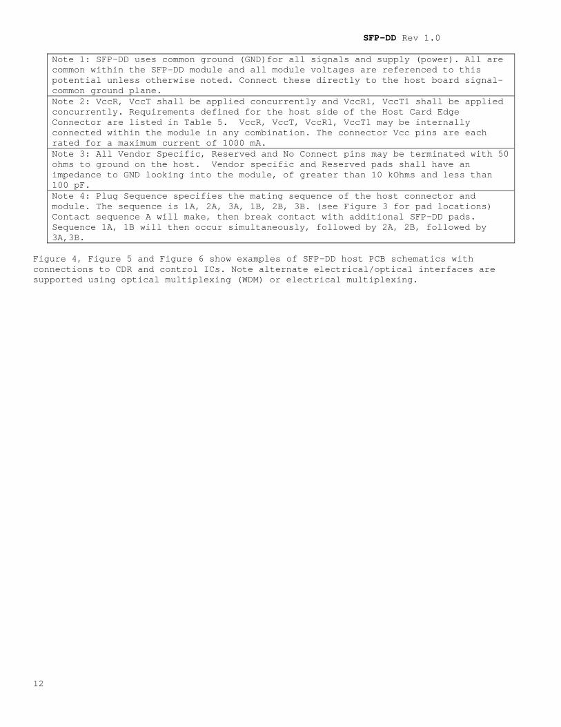
Note 1: SFP-DD uses common ground (GND)for all signals and supply (power). All are common within the SFP-DD module and all module voltages are referenced to this potential unless otherwise noted. Connect these directly to the host board signal-common ground plane. Note 2: VccR, VccT shall be applied concurrently and VccR1, VccT1 shall be applied concurrently. Requirements defined for the host side of the Host Card Edge Connector are listed in Table 5. VccR, VccT, VccR1, VccT1 may be internally connected within the module in any combination. The connector Vcc pins are each rated for a maximum current of 1000 mA. Note 3: All Vendor Specific, Reserved and No Connect pins may be terminated with 50 ohms to ground on the host. Vendor specific and Reserved pads shall have an impedance to GND looking into the module, of greater than 10 kOhms and less than 100 pF. Note 4: Plug Sequence specifies the mating sequence of the host connector and module. The sequence is 1A, 2A, 3A, 1B, 2B, 3B. (see Figure 3 for pad locations) Contact sequence A will make, then break contact with additional SFP-DD pads. Sequence 1A, 1B will then occur simultaneously, followed by 2A, 2B, followed by 3A,3B.
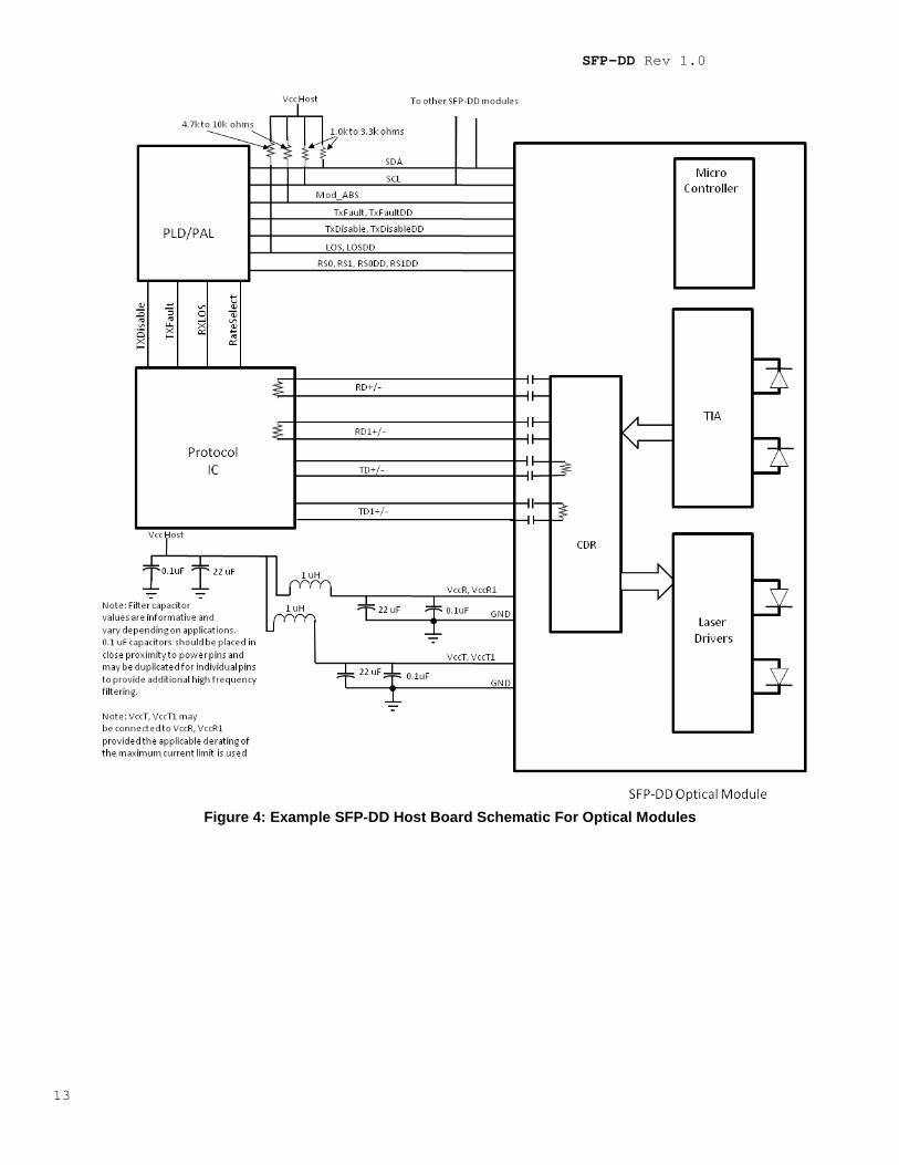
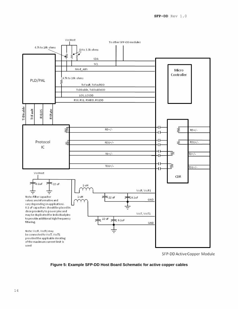
Figure 4, Figure 5 and Figure 6 show examples of SFP-DD host PCB schematics with connections to CDR and control ICs. Note alternate electrical/optical interfaces are supported using optical multiplexing (WDM) or electrical multiplexing.
SFP-DD Rev 1.0
13
Figure 4: Example SFP-DD Host Board Schematic For Optical Modules
SFP-DD Rev 1.0
14
Figure 5: Example SFP-DD Host Board Schematic for active copper cables
SFP-DD Rev 1.0
15
Figure 6: Example SFP-DD Host Board Schematic for passive copper cables
SFP-DD Rev 1.0
16
4.1.1 Low Speed Electrical Hardware Signals The module has the following low speed signals for control, status and management by the host: TxFault, TxFaultDD TxDisable, TxDisableDD SDA SCL Mod_ABS RS0,RS0DD RS1,RS1DD LOS, LOSDD IntL, InitMode
4.1.1.1 Tx_Fault, TxFaultDD Tx_Fault and TxFaultDD are module outputs that when high, indicate that the module transmitter has detected a fault condition related to laser operation or safety for the appropriate channel. If Tx_Fault and/or TxFaultDD are not implemented, the contact signal shall be held low by the module and may be connected to GND within the module. The Tx_Fault/TxFaultDD outputs are open drain/collector and shall be pulled up to the Vcc_Host in the host with a resistor in the range 4.7 kOhms to 10 kOhms, or with an active termination according to Table 2.
4.1.1.2 Tx_Disable, TxDisableDD When Tx_Disable or TxDisableDD are asserted high or left open, the appropriate SFP-DD module transmitter output shall be turned off unless the module is a passive cable assembly in which case this signal may be ignored. This contact shall be pulled up to VccT with a 4.7 kOhms to 10 kOhms resistor in modules and cable assemblies. Tx_Disable and TxDisableDD are module input contacts. When Tx_Disable or TxDisableDD are asserted low or grounded the module transmitter is operating normally.
4.1.1.3 RS0, RS0DD, RS1, RS1DD RS0, RS0DD, RS1 and RS1DD are module inputs and are pulled low to GND with >30 kOhms resistors in the module. RS0 optionally selects the optical receive signaling rate for the legacy channel. RS0DD optionally selects the optical receive signaling rate for the Double Density channel. RS1 optionally selects the optical transmit signaling rate for the legacy channel. RS1DD optionally selects the optical transmit signaling rate for the Double Density channel. For logical definitions of RS0/RS0DD/RS1/RS1DD see Section 4.2.
4.1.1.4 Mod_ABS Mod_ABS must be pulled up to Vcc Host on the host board and pulled low (see Table 2). The Mod_ABS is asserted “Low” when the module is inserted. The Mod_ABS is deasserted “High” when the module is physically absent from the host connector due to the pull up resistor on the host board.
4.1.1.5 SCL, SDA SCL is the 2-wire interface clock and SDA is the 2-wire interface data line. SCL and SDA are pulled up to Vcc_Host by resistors in the host. For full specifications see Section 5.
SFP-DD Rev 1.0
17
4.1.1.6 LOS, LOSDD Rx Loss of Signal indication. Logic 0 indicates normal operation. Open collector output. A resistive pull up to Vcc_Host the resistor value shall be use per Table 2. The Rx_LOS signal is intended as a preliminary indication to the host in which the module is installed that the received signal strength is below the specified range. Rx_LOS may be an optional function depending on the supported standard. If the Rx_LOS function is not implemented, or is reported via the two-wire interface only, the Rx_LOS contact shall be held low by the module and may be connected to GND within the module. Rx_LOS assert min and de-assert max are defined in the relevant standard. To avoid spurious transition of Rx_LOS a minimum hysteresis of 0.5 dBo is recommended.
4.1.1.7 InitMode InitMode is an input signal. The InitMode signal must be pulled up to Vcc in the SFP-DD module. The InitMode signal allows the host to define whether the SFP-DD module will initialize under host software control (InitMode asserted High) or module hardware control (InitMode deasserted Low). Under host software control, the module shall remain in Low Power Mode until software enables the transition to High Power Mode, as defined in the SFP-DD management specification. Under hardware control (InitMode de-asserted Low), the module may immediately transition to High Power Mode after the management interface is initialized. The host shall not change the state of this signal while the module is present.
4.1.1.8 IntL IntL is an output signal. The IntL signal is an open collector output and must be pulled to Vcc Host on the host board (see Table 2). When the IntL signal is asserted Low it indicates a change in module state, a possible module operational fault or a status critical to the host system. The host identifies the source of the interrupt using the 2-wire serial interface. The IntL signal is deasserted “High” after all set interrupt flags are read.
4.1.2 Low Speed Electrical Specification Low speed signaling other than the SCL and SDA interface is based on Low Voltage TTL (LVTTL) operating at a module supply Vcc of 3.3V +/- 5% and with a host supply Vcc_Host range of 2.38 to 3.46V. Vcc refers to the generic supply voltages of VccTx, VccRx, Vcc host or Vcc1.
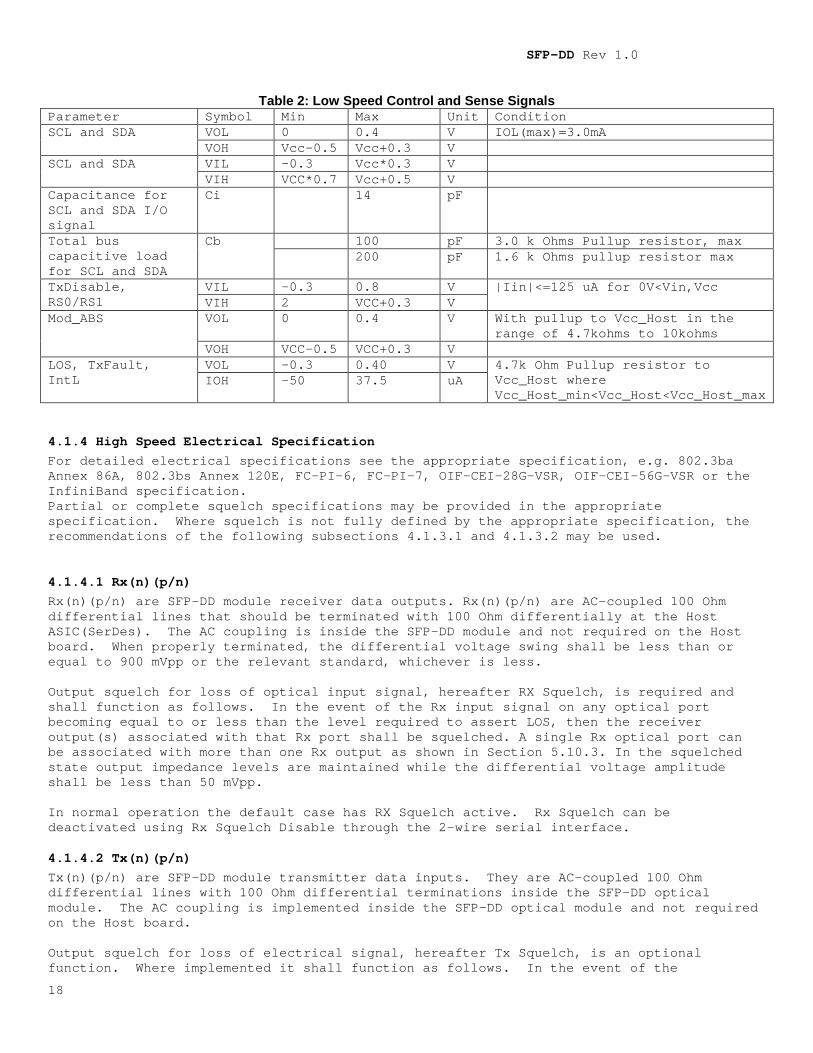
4.1.3 2 Wire Management Interface Specification The 2-wire interface protocol and timing specifications are defined in TBD. The SFP-DD low speed electrical specifications are given in Table 2. This specification ensures compatibility between host bus masters and the 2-wire interface.
SFP-DD Rev 1.0
18
Table 2: Low Speed Control and Sense Signals
Parameter Symbol Min Max Unit Condition SCL and SDA VOL 0 0.4 V IOL(max)=3.0mA
VOH Vcc-0.5 Vcc+0.3 V SCL and SDA VIL -0.3 Vcc*0.3 V
VIH VCC*0.7 Vcc+0.5 V Capacitance for SCL and SDA I/O signal
Ci 14 pF
Total bus capacitive load for SCL and SDA
Cb 100 pF 3.0 k Ohms Pullup resistor, max 200 pF 1.6 k Ohms pullup resistor max
TxDisable, RS0/RS1
VIL -0.3 0.8 V |Iin|<=125 uA for 0V<Vin,Vcc VIH 2 VCC+0.3 V
Mod_ABS VOL 0 0.4 V With pullup to Vcc_Host in the range of 4.7kohms to 10kohms
VOH VCC-0.5 VCC+0.3 V LOS, TxFault, IntL
VOL -0.3 0.40 V 4.7k Ohm Pullup resistor to Vcc_Host where Vcc_Host_min<Vcc_Host<Vcc_Host_max
IOH -50 37.5 uA
4.1.4 High Speed Electrical Specification For detailed electrical specifications see the appropriate specification, e.g. 802.3ba Annex 86A, 802.3bs Annex 120E, FC-PI-6, FC-PI-7, OIF-CEI-28G-VSR, OIF-CEI-56G-VSR or the InfiniBand specification. Partial or complete squelch specifications may be provided in the appropriate specification. Where squelch is not fully defined by the appropriate specification, the recommendations of the following subsections 4.1.3.1 and 4.1.3.2 may be used.
4.1.4.1 Rx(n)(p/n) Rx(n)(p/n) are SFP-DD module receiver data outputs. Rx(n)(p/n) are AC-coupled 100 Ohm differential lines that should be terminated with 100 Ohm differentially at the Host ASIC(SerDes). The AC coupling is inside the SFP-DD module and not required on the Host board. When properly terminated, the differential voltage swing shall be less than or equal to 900 mVpp or the relevant standard, whichever is less. Output squelch for loss of optical input signal, hereafter RX Squelch, is required and shall function as follows. In the event of the Rx input signal on any optical port becoming equal to or less than the level required to assert LOS, then the receiver output(s) associated with that Rx port shall be squelched. A single Rx optical port can be associated with more than one Rx output as shown in Section 5.10.3. In the squelched state output impedance levels are maintained while the differential voltage amplitude shall be less than 50 mVpp. In normal operation the default case has RX Squelch active. Rx Squelch can be deactivated using Rx Squelch Disable through the 2-wire serial interface.
4.1.4.2 Tx(n)(p/n) Tx(n)(p/n) are SFP-DD module transmitter data inputs. They are AC-coupled 100 Ohm differential lines with 100 Ohm differential terminations inside the SFP-DD optical module. The AC coupling is implemented inside the SFP-DD optical module and not required on the Host board. Output squelch for loss of electrical signal, hereafter Tx Squelch, is an optional function. Where implemented it shall function as follows. In the event of the
SFP-DD Rev 1.0
19
differential, peak-to-peak electrical signal amplitude on any electrical input channel becoming less than 70 mVpp, then the transmitter optical output associated with that electrical input channel shall be squelched and the associated TxLOS flag set. If multiple electrical input channels are associated with the same optical output channel, the loss of any of the incoming electrical input channels causes the optical output channel to be squelched. For applications, e.g. Ethernet, where the transmitter off condition is defined in terms of average power, squelching by disabling the transmitter is recommended and for applications, e.g. InfiniBand, where the transmitter off condition is defined in terms of OMA, squelching the transmitter by setting the OMA to a low level is recommended. In module operation, where Tx Squelch is implemented, the default case has Tx Squelch active. Tx Squelch can be deactivated using Tx Squelch Disable through the 2-wire serial interface. Tx Squelch is an optional function. If TX squelch is implemented, the disable squelch must be provided.
4.2 Rate Select Hardware Control The module provides 4 inputs RS0, RS1, RS0DD and RS1DD that can optionally be used for rate selection as defined in Table 3. RS0 controls the receive path signaling rate capability for the legacy SFP receive path. RS0DD controls the receive path signaling rate capability for the DD receive path. Similarly, RS1 controls the transmit path signaling rate capability for the legacy SFP and RS1DD controls the transmit path signaling rate capability for the DD transmit path. The rate select functionality can also be controlled by software as defined by the SFP-DD management specification. The Rate select Hardware Control is intended to be compatible with Fibre Channel 64GFC rate select methodology.
Table 3: Rate Select Hardware Control Parameter State Conditions RS0, RS0DD Low RX signaling rate of 14Gbaud
High RX signaling rate of 28Gbaud RS1, RS1DD Low TX signaling rate of 14Gbaud
High TX signaling rate of 28Gbaud
4.3 Power Requirements The power supply has four designated pins, VccT, VccT1 VccR, VccR1 in the connector. Power is applied concurrently to VccT, VccR in the legacy row and concurrently to VccT1, VccR1 in the DD row. A host board together with the SFP-DD module(s) forms an integrated power system. The host supplies stable power to the module. The module limits electrical noise coupled back into the host system and limits inrush charge/current during hot plug insertion. All power supply requirements in Table 5 shall be met at the maximum power supply current. No power sequencing of the power supply is required of the host system since the module sequences the contacts in the order of ground, supply and signals during insertion.
SFP-DD Rev 1.0
20
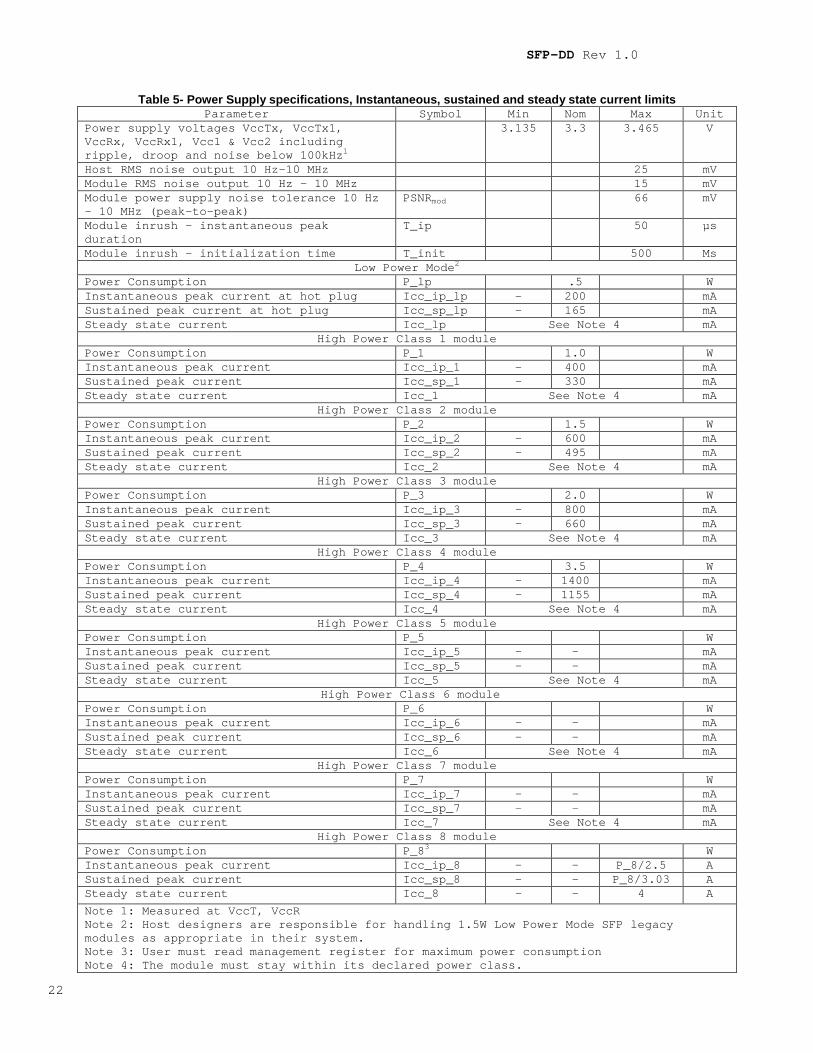
4.3.1 Power Classes and Maximum Power Consumption There are multiple power classes as defined in Table 4. Since different classes of modules exist with pre-defined maximum power consumption limits, it is necessary to avoid exceeding the system power supply limits and cooling capacity when a module is inserted into a system designed to only accommodate lower power modules. It is recommended that the host implement the state machine recommended in the SFP-DD management specification and identify the power class of the module before allowing the module to go into high power mode. Power levels associated with classifications of modules are shown in Table 4.
Table 4- Power Classification Power Class Max Power (W) 1 1.0 2 1.5 3 2.0 4 3.5 5 6 7 8
In general, the higher power classification levels are associated with higher data rates and longer reaches. The system designer is responsible for ensuring that the maximum case temperature does not exceed the case temperature requirements.
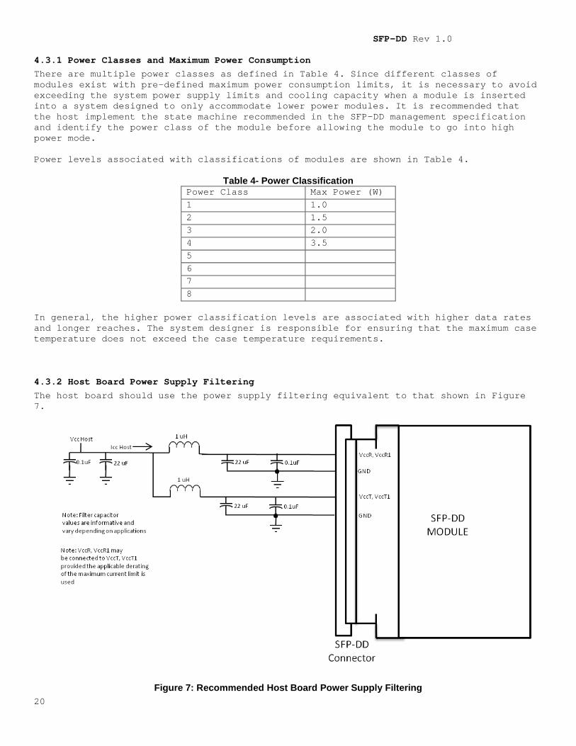
4.3.2 Host Board Power Supply Filtering The host board should use the power supply filtering equivalent to that shown in Figure 7.
Figure 7: Recommended Host Board Power Supply Filtering
SFP-DD Rev 1.0
21
Any voltage drop across a filter network on the host is counted against the host DC set point accuracy specification. Inductors with DC Resistance of less than 0.1 Ohm should be used in order to maintain the required voltage at the Host Card Edge Connector. It is recommended that the 22 uF capacitors each have an equivalent series resistance of 0.22 ohm. The specifications for the power supply are shown in Table 5. The limits in Table 5 apply to the combined current that flows through all inductors in the power supply filter (represents ICC host in Figure 7). The test method for measuring inrush current can be found in Keysight Technologies application brief 5991-2778EN.pdf.
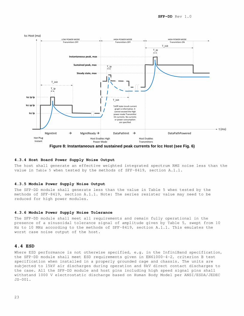
4.3.3 Module Power Supply Specification In order to avoid exceeding the host system power capacity, upon hot-plug, power cycle or reset, all SFP-DD modules shall power up in Low Power Mode if InitMode is asserted. If InitMode is not asserted the module will proceed to High Power Mode without host intervention. Figure 8 shows waveforms for maximum instantaneous, sustained and steady state currents for Low Power and High Power modes. Specification values for maximum instantaneous, sustained and steady state currents at each power class are given in Table 5.
SFP-DD Rev 1.0
22
Table 5- Power Supply specifications, Instantaneous, sustained and steady state current limits
Parameter Symbol Min Nom Max Unit Power supply voltages VccTx, VccTx1, VccRx, VccRx1, Vcc1 & Vcc2 including ripple, droop and noise below 100kHz1
3.135 3.3 3.465 V
Host RMS noise output 10 Hz-10 MHz 25 mV Module RMS noise output 10 Hz - 10 MHz 15 mV Module power supply noise tolerance 10 Hz - 10 MHz (peak-to-peak)
PSNRmod 66 mV
Module inrush - instantaneous peak duration
T_ip 50 µs
Module inrush - initialization time T_init 500 Ms Low Power Mode2
Power Consumption P_lp .5 W Instantaneous peak current at hot plug Icc_ip_lp - 200 mA Sustained peak current at hot plug Icc_sp_lp - 165 mA Steady state current Icc_lp See Note 4 mA
High Power Class 1 module Power Consumption P_1 1.0 W Instantaneous peak current Icc_ip_1 - 400 mA Sustained peak current Icc_sp_1 - 330 mA Steady state current Icc_1 See Note 4 mA
High Power Class 2 module Power Consumption P_2 1.5 W Instantaneous peak current Icc_ip_2 - 600 mA Sustained peak current Icc_sp_2 - 495 mA Steady state current Icc_2 See Note 4 mA
High Power Class 3 module Power Consumption P_3 2.0 W Instantaneous peak current Icc_ip_3 - 800 mA Sustained peak current Icc_sp_3 - 660 mA Steady state current Icc_3 See Note 4 mA
High Power Class 4 module Power Consumption P_4 3.5 W Instantaneous peak current Icc_ip_4 - 1400 mA Sustained peak current Icc_sp_4 - 1155 mA Steady state current Icc_4 See Note 4 mA
High Power Class 5 module Power Consumption P_5 W Instantaneous peak current Icc_ip_5 - - mA Sustained peak current Icc_sp_5 - - mA Steady state current Icc_5 See Note 4 mA
High Power Class 6 module Power Consumption P_6 W Instantaneous peak current Icc_ip_6 - - mA Sustained peak current Icc_sp_6 - - mA Steady state current Icc_6 See Note 4 mA
High Power Class 7 module Power Consumption P_7 W Instantaneous peak current Icc_ip_7 - - mA Sustained peak current Icc_sp_7 - - mA Steady state current Icc_7 See Note 4 mA
High Power Class 8 module Power Consumption P_83 W Instantaneous peak current Icc_ip_8 - - P_8/2.5 A Sustained peak current Icc_sp_8 - - P_8/3.03 A Steady state current Icc_8 - - 4 A
Note 1: Measured at VccT, VccR Note 2: Host designers are responsible for handling 1.5W Low Power Mode SFP legacy modules as appropriate in their system. Note 3: User must read management register for maximum power consumption Note 4: The module must stay within its declared power class.
SFP-DD Rev 1.0
23
Instantaneous peak, max
Sustained peak, max
Steady state, max
Icc ip lp
Icc sp lp
Icc lp
LOW POWER MODETransmitters OFF
HIGH POWER MODETransmitters ON
Icc Host (ma)
t (ms)MgmtInit à MgmtReady à
Hot PlugInstant
Host Enables High Power Mode
T_ip
Host Enables Transmitters
HIGH POWER MODETransmitters OFF
T_init
T_ipT_init
DataPathPowered
T_init
T_ip
TxOff state inrush current graph is informative. It cannot exceed the High
power mode Transmitter On currents. No currents or power consumption
are specified
DataPathInit à
Figure 8: Instantaneous and sustained peak currents for Icc Host (see Fig. 6)
4.3.4 Host Board Power Supply Noise Output The host shall generate an effective weighted integrated spectrum RMS noise less than the value in Table 5 when tested by the methods of SFF-8419, section A.1.1.
4.3.5 Module Power Supply Noise Output The SFP-DD module shall generate less than the value in Table 5 when tested by the methods of SFF-8419, section A.1.1. Note: The series resister value may need to be reduced for high power modules.
4.3.6 Module Power Supply Noise Tolerance The SFP-DD module shall meet all requirements and remain fully operational in the presence of a sinusoidal tolerance signal of amplitude given by Table 5, swept from 10 Hz to 10 MHz according to the methods of SFF-8419, section A.1.1. This emulates the worst case noise output of the host.
4.4 ESD Where ESD performance is not otherwise specified, e.g. in the InfiniBand specification, the SFP-DD module shall meet ESD requirements given in EN61000-4-2, criterion B test specification when installed in a properly grounded cage and chassis. The units are subjected to 15kV air discharges during operation and 8kV direct contact discharges to the case. All the SFP-DD module and host pins including high speed signal pins shall withstand 1000 V electrostatic discharge based on Human Body Model per ANSI/ESDA/JEDEC JS-001.
SFP-DD Rev 1.0
24
5 Mechanical and Board Definition
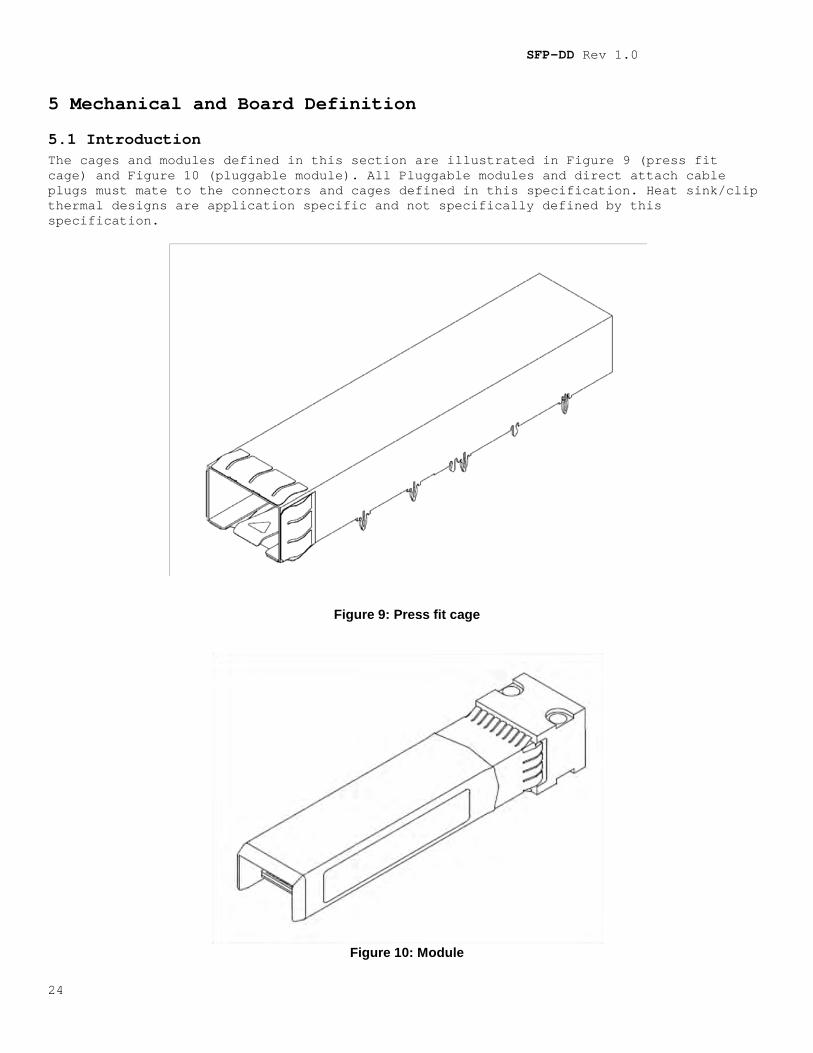
5.1 Introduction The cages and modules defined in this section are illustrated in Figure 9 (press fit cage) and Figure 10 (pluggable module). All Pluggable modules and direct attach cable plugs must mate to the connectors and cages defined in this specification. Heat sink/clip thermal designs are application specific and not specifically defined by this specification.
Figure 9: Press fit cage
Figure 10: Module
SFP-DD Rev 1.0
25
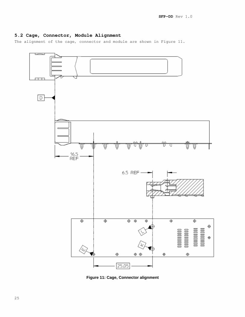
5.2 Cage, Connector, Module Alignment The alignment of the cage, connector and module are shown in Figure 11.
Figure 11: Cage, Connector alignment
SFP-DD Rev 1.0
26
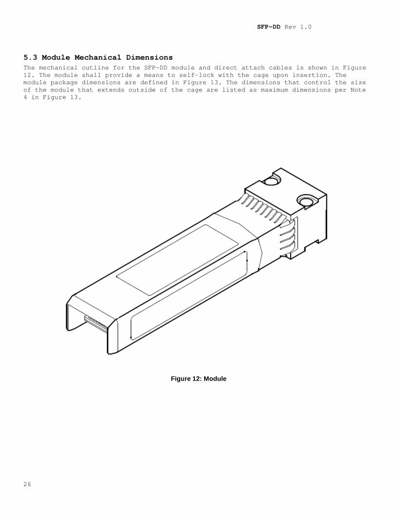
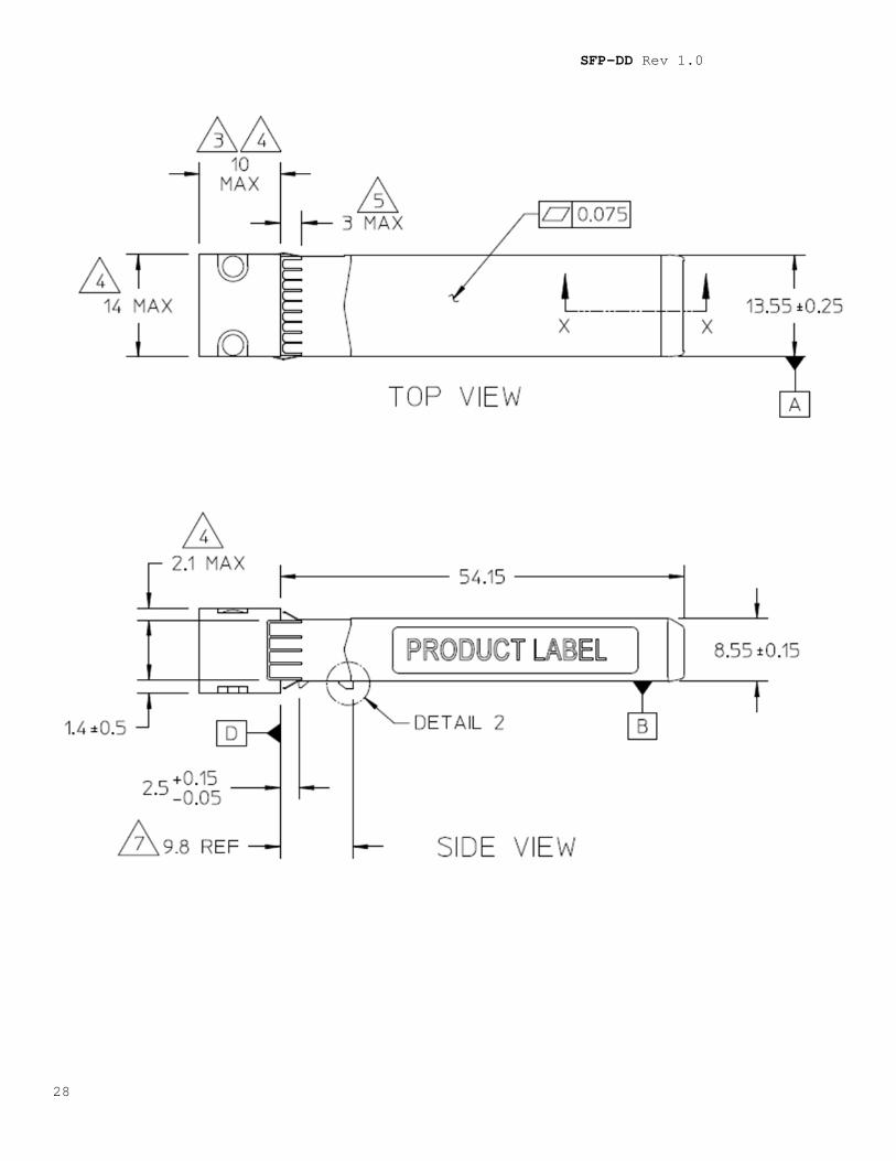
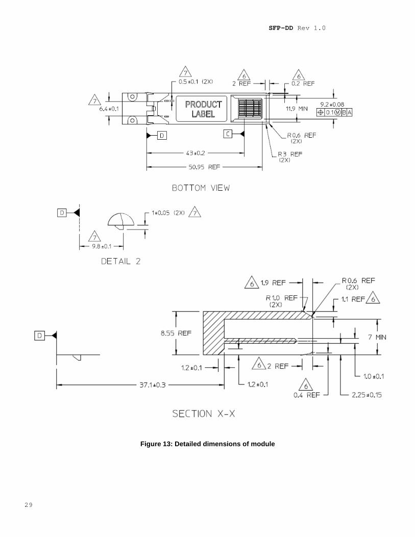
5.3 Module Mechanical Dimensions The mechanical outline for the SFP-DD module and direct attach cables is shown in Figure 12. The module shall provide a means to self-lock with the cage upon insertion. The module package dimensions are defined in Figure 13. The dimensions that control the size of the module that extends outside of the cage are listed as maximum dimensions per Note 4 in Figure 13.
Figure 12: Module
SFP-DD Rev 1.0
27
SFP-DD Rev 1.0
28
SFP-DD Rev 1.0
29
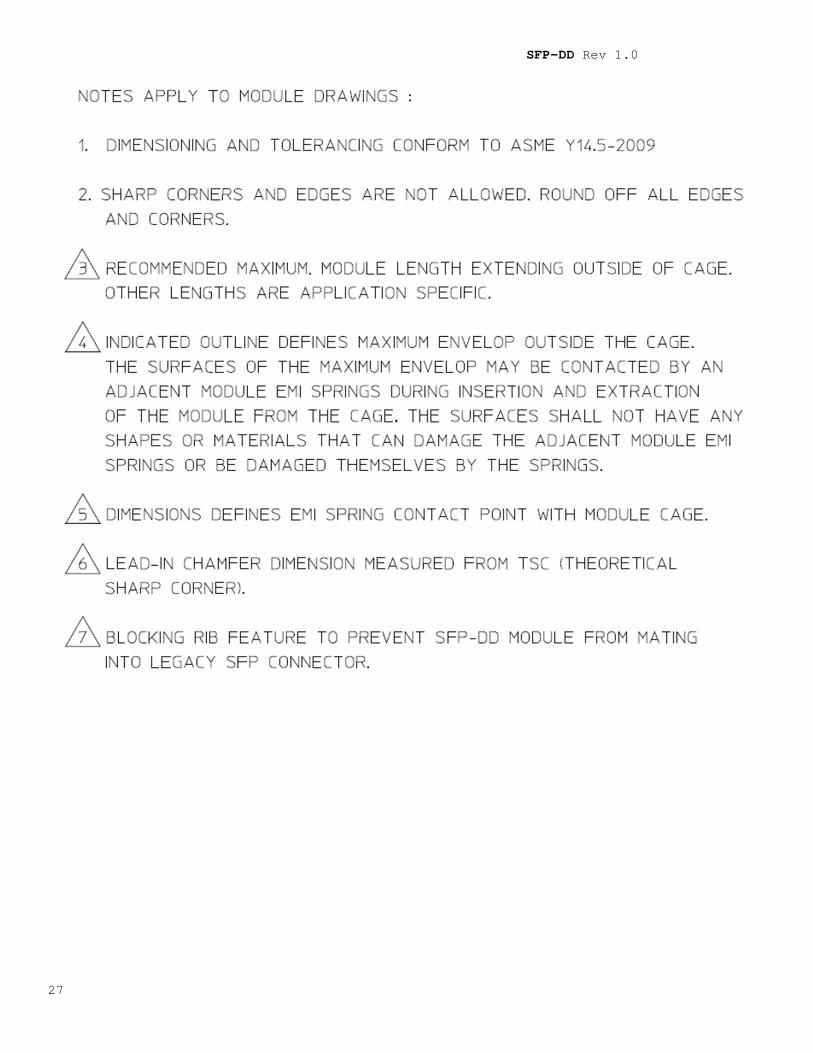
Figure 13: Detailed dimensions of module
SFP-DD Rev 1.0
30
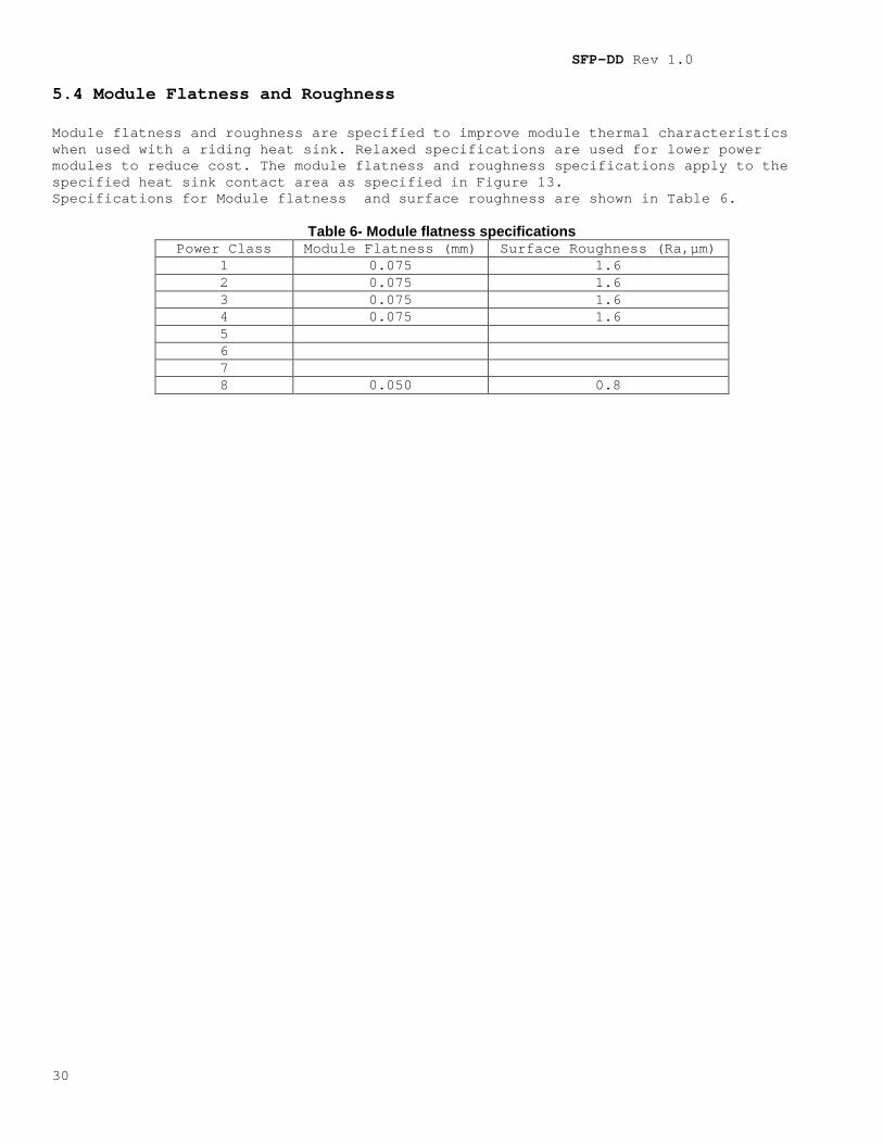
5.4 Module Flatness and Roughness Module flatness and roughness are specified to improve module thermal characteristics when used with a riding heat sink. Relaxed specifications are used for lower power modules to reduce cost. The module flatness and roughness specifications apply to the specified heat sink contact area as specified in Figure 13. Specifications for Module flatness and surface roughness are shown in Table 6.
Table 6- Module flatness specifications Power Class Module Flatness (mm) Surface Roughness (Ra,µm)
1 0.075 1.6 2 0.075 1.6 3 0.075 1.6 4 0.075 1.6 5 6 7 8 0.050 0.8
SFP-DD Rev 1.0
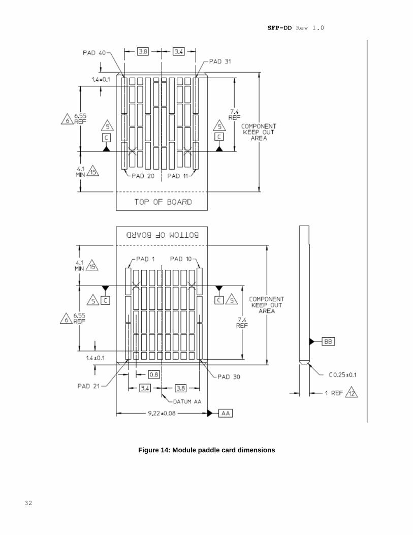
31
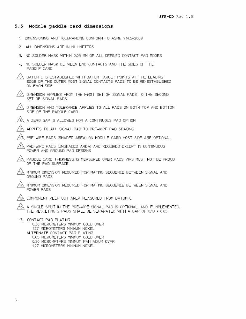
5.5 Module paddle card dimensions
SFP-DD Rev 1.0
32
Figure 14: Module paddle card dimensions
SFP-DD Rev 1.0
33
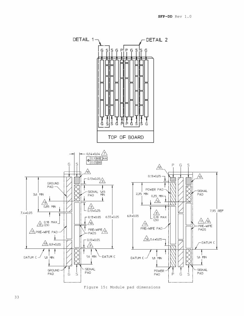
Figure 15: Module pad dimensions
SFP-DD Rev 1.0
34
5.6 Module Extraction and Retention Forces The requirements for insertion forces, extraction forces and retention forces are specified in Table 7. The SFP-DD cage and module are designed to ensure that excessive force applied to a cable does not damage the SFP-DD cage or host connector. If any part is damaged by excessive force, it should be the cable or media module and not the cage or host connector which is part of the host system. The contact pad plating shall meet the requirements of Section 5.5.
Table 7- Insertion, Extraction and Retention Forces Measurement Min Max Units Comments SFP module insertion 0 18 N SFP-DD module insertion
0 40 N
SFP module extraction 0 12.5 N SFP-DD module extraction
0 30 N
SFP module retention 90 N/A N No damage to module below 90N with latch engaged
SFP-DD module retention
90 N/A N No damage to module below 90N with latch engaged
Cage retention in Host Board
100 N/A N Force to be applied in a vertical direction, no damage to cage
Insertion / removal cycles, connector / cage
100 N/A Cycles Number of cycles for the connector and cage with multiple modules.
Insertion / removal cycles, SFP-DD module
50 N/A Cycles Number of cycles for an individual module.
Note: Insertion, Extraction and Retention forces are absolute values. (must comply with or without a riding heat sink)
SFP-DD Rev 1.0
35
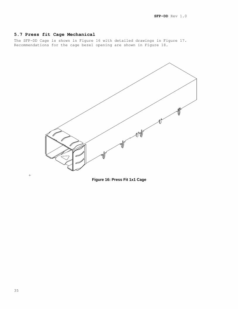
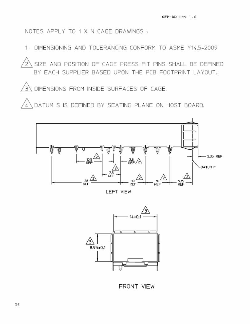
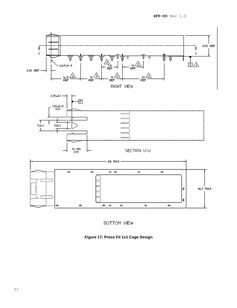
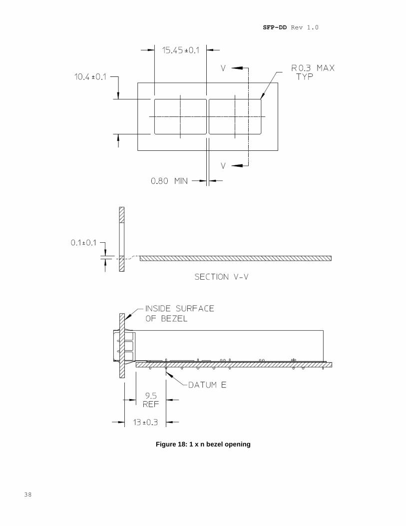
5.7 Press fit Cage Mechanical The SFP-DD Cage is shown in Figure 16 with detailed drawings in Figure 17. Recommendations for the cage bezel opening are shown in Figure 18.
+ Figure 16: Press Fit 1x1 Cage
SFP-DD Rev 1.0
36
SFP-DD Rev 1.0
37
Figure 17: Press Fit 1x1 Cage Design
SFP-DD Rev 1.0
38
Figure 18: 1 x n bezel opening
SFP-DD Rev 1.0
39
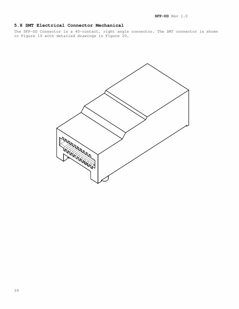
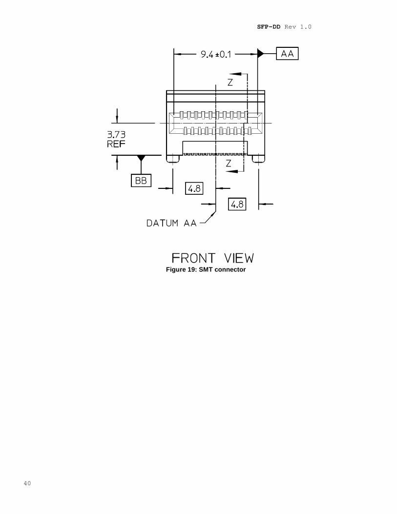
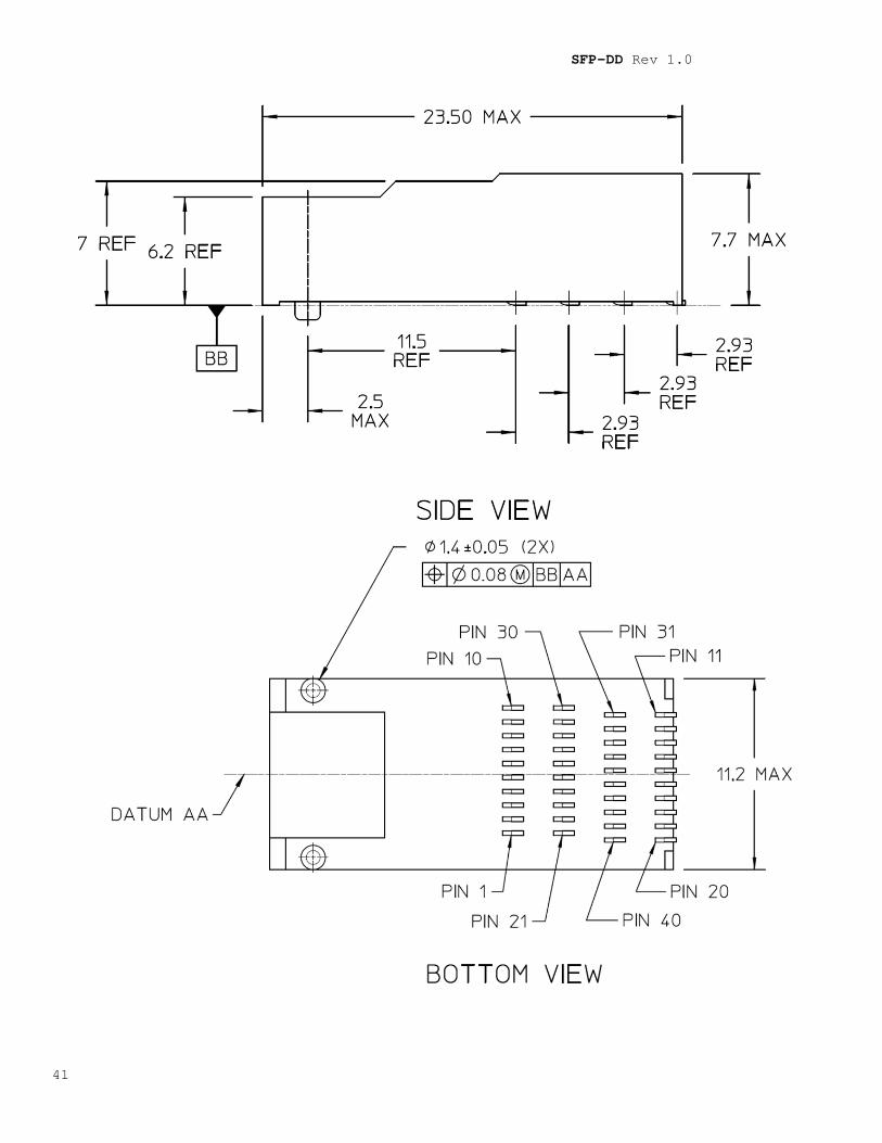
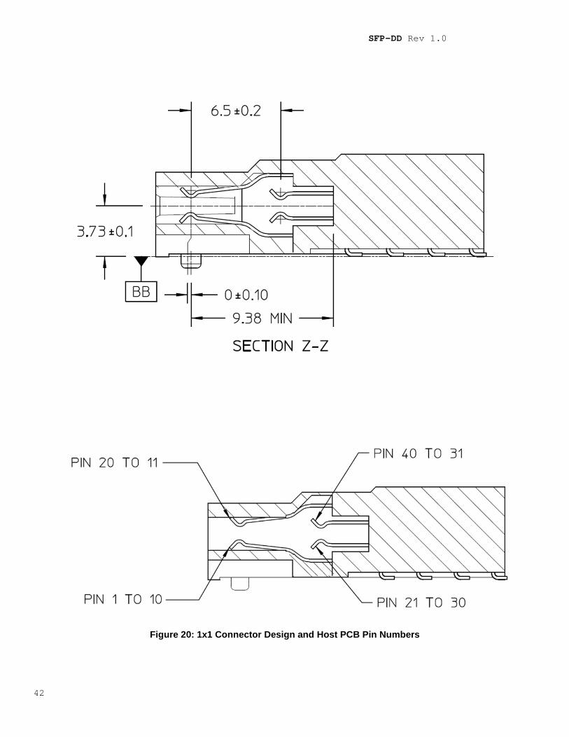
5.8 SMT Electrical Connector Mechanical The SFP-DD Connector is a 40-contact, right angle connector. The SMT connector is shown in Figure 19 with detailed drawings in Figure 20.
SFP-DD Rev 1.0
40
Figure 19: SMT connector
SFP-DD Rev 1.0
41
SFP-DD Rev 1.0
42
Figure 20: 1x1 Connector Design and Host PCB Pin Numbers
SFP-DD Rev 1.0
43
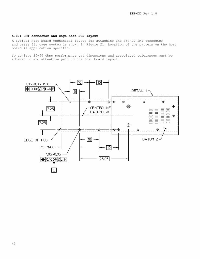
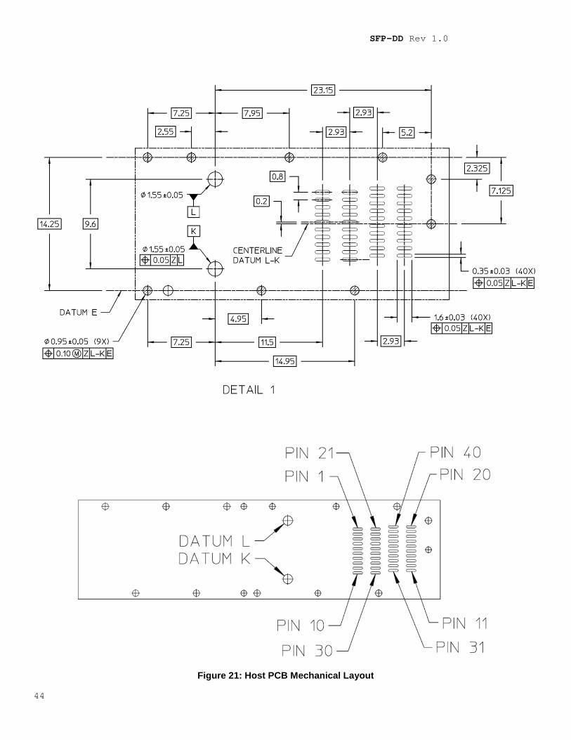
5.8.1 SMT connector and cage host PCB layout A typical host board mechanical layout for attaching the SFP-DD SMT connector and press fit cage system is shown in Figure 21. Location of the pattern on the host board is application specific. To achieve 25-50 Gbps performance pad dimensions and associated tolerances must be adhered to and attention paid to the host board layout.
SFP-DD Rev 1.0
44
Figure 21: Host PCB Mechanical Layout
SFP-DD Rev 1.0
45
5.9 Module Color Coding and Labeling If provided, color coding shall be on an exposed feature of the SFP-DD module (a feature or surface extending outside of the bezel). Color code are outside the scope of this specification. Each SFP-DD module shall be clearly labeled. The complete labeling need not be visible when the SFP-DD module is installed and the bottom of the device is the recommended location for the label. Labeling shall include:
Appropriate manufacturing and part number identification Appropriate regulatory compliance labeling A manufacturing traceability code
The label should also include clear specification of the external port characteristics such as:
Optical wavelength Required fiber characteristics Operating data rate Interface standards supported Link length supported
The labeling shall not interfere with the mechanical, thermal or EMI features.
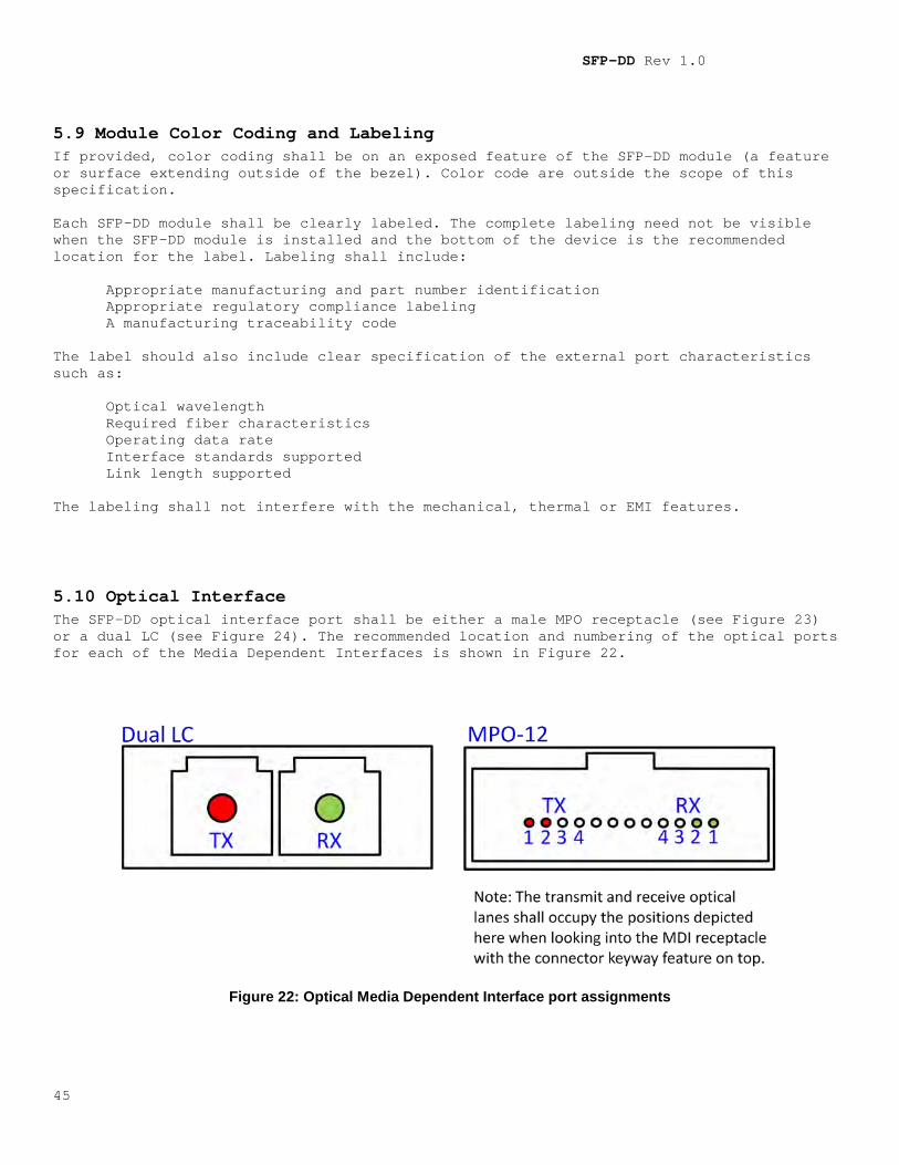
5.10 Optical Interface The SFP-DD optical interface port shall be either a male MPO receptacle (see Figure 23) or a dual LC (see Figure 24). The recommended location and numbering of the optical ports for each of the Media Dependent Interfaces is shown in Figure 22.
Figure 22: Optical Media Dependent Interface port assignments
SFP-DD Rev 1.0
46
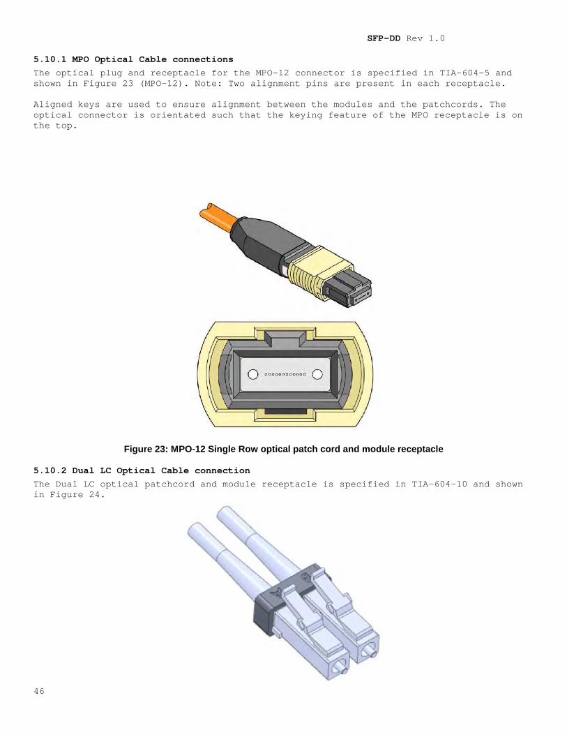
5.10.1 MPO Optical Cable connections The optical plug and receptacle for the MPO-12 connector is specified in TIA-604-5 and shown in Figure 23 (MPO-12). Note: Two alignment pins are present in each receptacle. Aligned keys are used to ensure alignment between the modules and the patchcords. The optical connector is orientated such that the keying feature of the MPO receptacle is on the top.
Figure 23: MPO-12 Single Row optical patch cord and module receptacle
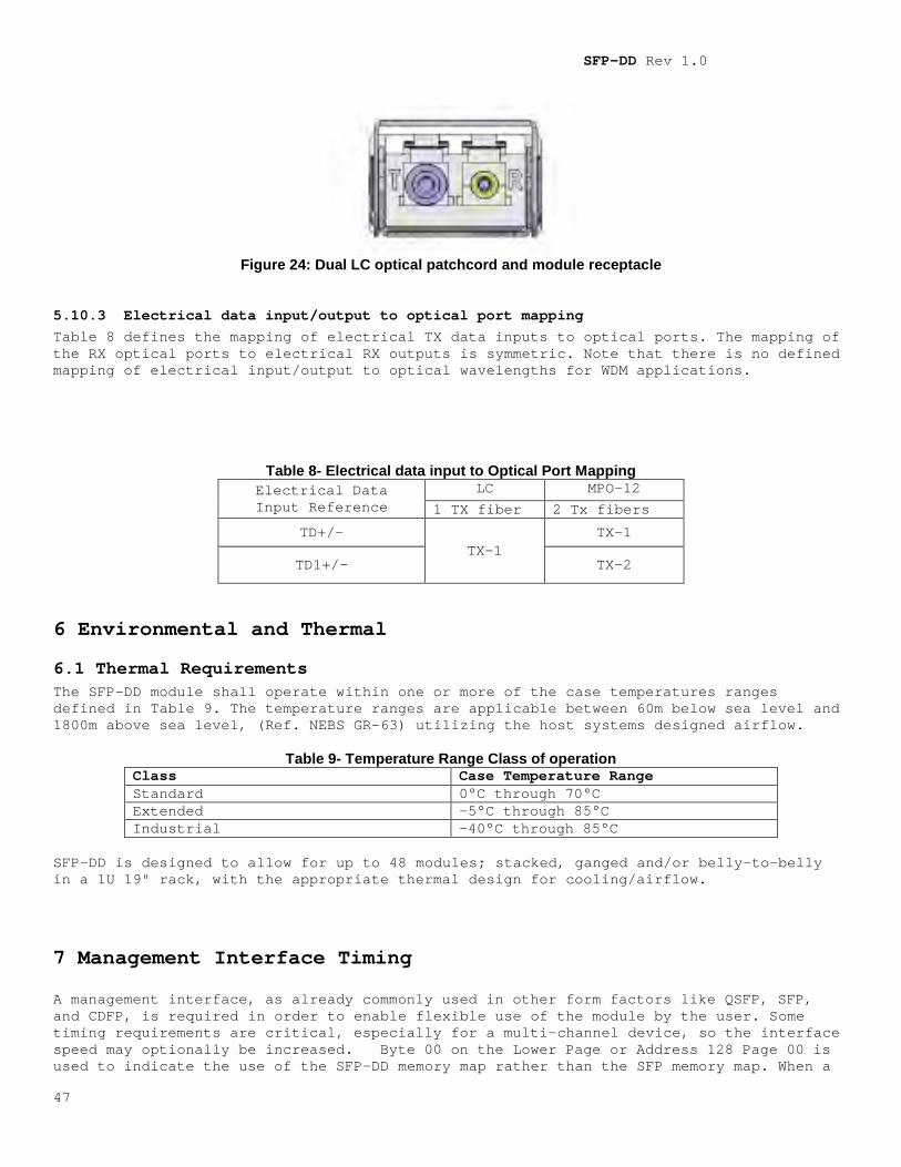
5.10.2 Dual LC Optical Cable connection The Dual LC optical patchcord and module receptacle is specified in TIA-604-10 and shown in Figure 24.
SFP-DD Rev 1.0
47
Figure 24: Dual LC optical patchcord and module receptacle
5.10.3 Electrical data input/output to optical port mapping Table 8 defines the mapping of electrical TX data inputs to optical ports. The mapping of the RX optical ports to electrical RX outputs is symmetric. Note that there is no defined mapping of electrical input/output to optical wavelengths for WDM applications.
Table 8- Electrical data input to Optical Port Mapping Electrical Data Input Reference
LC MPO-12
1 TX fiber 2 Tx fibers
TD+/- TX-1
TX-1
TD1+/- TX-2
6 Environmental and Thermal
6.1 Thermal Requirements The SFP-DD module shall operate within one or more of the case temperatures ranges defined in Table 9. The temperature ranges are applicable between 60m below sea level and 1800m above sea level, (Ref. NEBS GR-63) utilizing the host systems designed airflow.
Table 9- Temperature Range Class of operation Class Case Temperature Range Standard 0°C through 70°C Extended -5°C through 85°C Industrial -40°C through 85°C
SFP-DD is designed to allow for up to 48 modules; stacked, ganged and/or belly-to-belly in a 1U 19" rack, with the appropriate thermal design for cooling/airflow.
7 Management Interface Timing A management interface, as already commonly used in other form factors like QSFP, SFP, and CDFP, is required in order to enable flexible use of the module by the user. Some timing requirements are critical, especially for a multi-channel device, so the interface speed may optionally be increased. Byte 00 on the Lower Page or Address 128 Page 00 is used to indicate the use of the SFP-DD memory map rather than the SFP memory map. When a
SFP-DD Rev 1.0
48
legacy SFP28 module is inserted into a SFP-DD port the legacy SFP memory map (i.e. SFF-8472) must be used. This case is outside the scope of this document. In some applications, muxing or demuxing may occur in the module. In this specification, all references to channel numbers are based on the electrical connector interface channels, unless otherwise indicated. In cases where a status or control aspect is applicable only to channels after muxing or demuxing has occurred, the status or control is intended to apply to all channels in the mux group, unless otherwise indicated.
7.1 SCL and SDA Timing Specification
7.1.1 Introduction Low speed signaling is based on Low Voltage CMOS (LVCMOS) operating at Vcc. Hosts shall use a pull-up resistor connected to Vcc_host on the 2-wire interface SCL (clock) and SDA (Data) signals. Detailed electrical specifications are given in SFF-8679 Subsection 5.3.
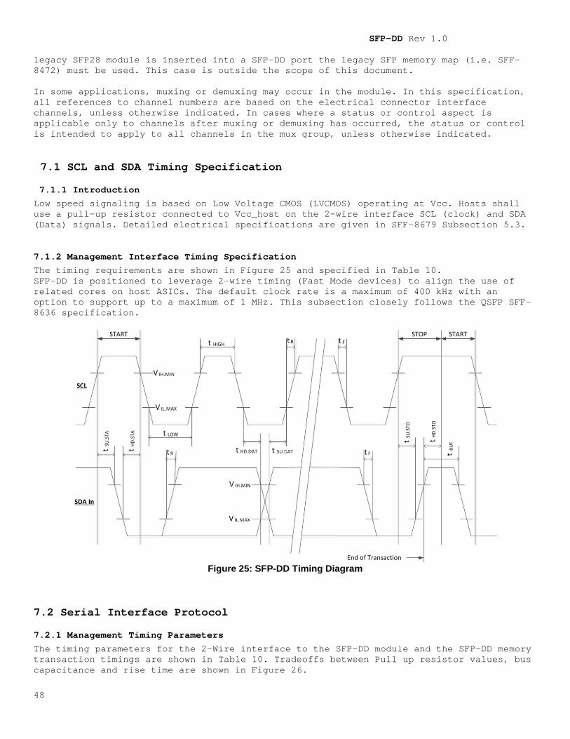
7.1.2 Management Interface Timing Specification The timing requirements are shown in Figure 25 and specified in Table 10. SFP-DD is positioned to leverage 2-wire timing (Fast Mode devices) to align the use of related cores on host ASICs. The default clock rate is a maximum of 400 kHz with an option to support up to a maximum of 1 MHz. This subsection closely follows the QSFP SFF-8636 specification.
Figure 25: SFP-DD Timing Diagram
7.2 Serial Interface Protocol
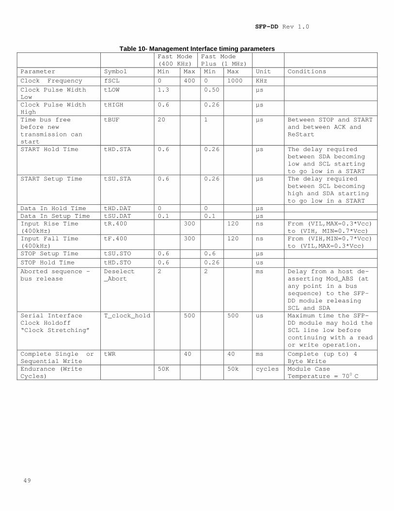
7.2.1 Management Timing Parameters The timing parameters for the 2-Wire interface to the SFP-DD module and the SFP-DD memory transaction timings are shown in Table 10. Tradeoffs between Pull up resistor values, bus capacitance and rise time are shown in Figure 26.
SFP-DD Rev 1.0
49
Table 10- Management Interface timing parameters
Fast Mode (400 KHz)
Fast Mode Plus (1 MHz)
Parameter Symbol Min Max Min Max Unit Conditions
Clock Frequency fSCL 0 400 0 1000 KHz Clock Pulse Width Low
tLOW 1.3 0.50 µs
Clock Pulse Width High
tHIGH 0.6 0.26 µs
Time bus free before new transmission can start
tBUF 20 1 µs Between STOP and START and between ACK and ReStart
START Hold Time tHD.STA 0.6 0.26 µs The delay required between SDA becoming low and SCL starting to go low in a START
START Setup Time tSU.STA 0.6 0.26 µs The delay required between SCL becoming high and SDA starting to go low in a START
Data In Hold Time tHD.DAT 0 0 µs Data In Setup Time tSU.DAT 0.1 0.1 µs Input Rise Time (400kHz)
tR.400 300 120 ns From (VIL,MAX=0.3*Vcc) to (VIH, MIN=0.7*Vcc)
Input Fall Time (400kHz)
tF.400 300 120 ns From (VIH,MIN=0.7*Vcc) to (VIL,MAX=0.3*Vcc)
STOP Setup Time tSU.STO 0.6 0.6 µs STOP Hold Time tHD.STO 0.6 0.26 us Aborted sequence – bus release
Deselect _Abort
2 2 ms Delay from a host de-asserting Mod_ABS (at any point in a bus sequence) to the SFP-DD module releasing SCL and SDA
Serial Interface Clock Holdoff “Clock Stretching”
T_clock_hold 500 500 us Maximum time the SFP-DD module may hold the SCL line low before continuing with a read or write operation.
Complete Single or Sequential Write
tWR 40 40 ms Complete (up to) 4 Byte Write
Endurance (Write Cycles)
50K 50k cycles Module Case Temperature = 700 C
SFP-DD Rev 1.0
50
Figure 26: SDA/SCL options for pull-up resistor, bus capacitance and rise/fall times
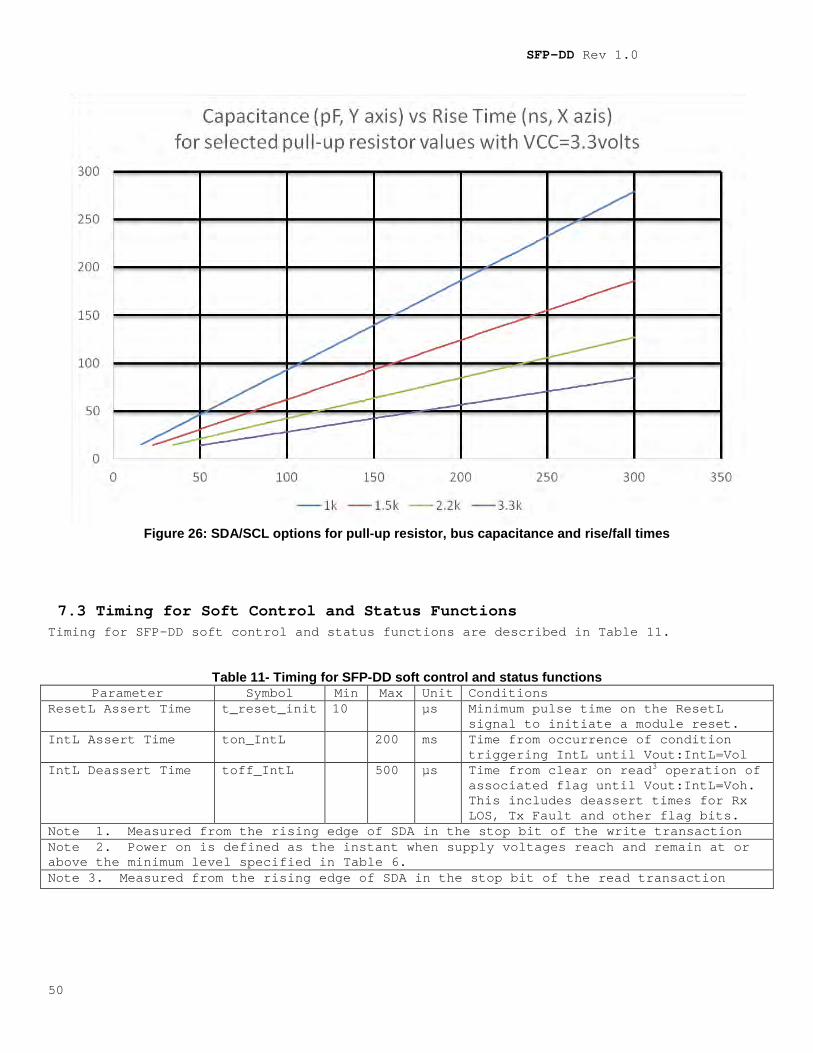
7.3 Timing for Soft Control and Status Functions Timing for SFP-DD soft control and status functions are described in Table 11.
Table 11- Timing for SFP-DD soft control and status functions Parameter Symbol Min Max Unit Conditions
ResetL Assert Time t_reset_init 10 µs Minimum pulse time on the ResetL signal to initiate a module reset.
IntL Assert Time ton_IntL 200 ms Time from occurrence of condition triggering IntL until Vout:IntL=Vol
IntL Deassert Time toff_IntL 500 µs Time from clear on read3 operation of associated flag until Vout:IntL=Voh. This includes deassert times for Rx LOS, Tx Fault and other flag bits.
Note 1. Measured from the rising edge of SDA in the stop bit of the write transaction Note 2. Power on is defined as the instant when supply voltages reach and remain at or above the minimum level specified in Table 6. Note 3. Measured from the rising edge of SDA in the stop bit of the read transaction