pn Junctions - pages.hep.wisc.edu
28
pn Junctions Murray Thompson Sept. 13, 1999 Contents 1 Introduction 1 2 Multiple One Dimensional Potential Wells 1 3 Multiple Three Dimensional Potential Wells 2 4 Fermi Level 2 5 Semiconductors 2 6 p Type and n Type Materials 2 7 Donor Levels in n type Material 3 8 Electrons and Holes 4 9 Acceptor Levels in p type Material 5 10 Adjacent p and n Type material 6 11 p and n Types in Contact 9 12 Now Raise the voltage of the p Type by V 15 13 Dynamic Resistance of the PN Junction 19 14 Energy Levels in Junctions 21 1
Transcript of pn Junctions - pages.hep.wisc.edu
pn Junctions
Murray Thompson
Sept. 13, 1999
Contents
1 Introduction 1
2 Multiple One Dimensional Potential Wells 1
3 Multiple Three Dimensional Potential Wells 2
4 Fermi Level 2
5 Semiconductors 2
6 p Type and n Type Materials 2
7 Donor Levels in n type Material 3
8 Electrons and Holes 4
9 Acceptor Levels in p type Material 5
10 Adjacent p and n Type material 6
11 p and n Types in Contact 9
12 Now Raise the voltage of the p Type by V 15
13 Dynamic Resistance of the PN Junction 19
14 Energy Levels in Junctions 21
1
15 Two pn Junctions 25
16 An npn Junction Transistor 27
1 Introduction
This is a non-rigorous explanation to give you an understanding of the back-ground for the operation of semiconductor diodes and the Diode Equation.This explanation is intended to fill in part of the missing background inH& H. We advise 623 students to read R.E. Simpson’s book “IntroductoryElectronics for Scientists and Engineers” pages 162 – 185.
Since this explanation is an addition to the lectures in which pn junctionsare discussed, it assumes some of the material from the 623 lectures plussome material from the other physics courses and is not intended to be a fullexplanation of pn junctions.
2 Multiple One Dimensional Potential Wells
In Quantum Mechanics, we learn how the wavefunctions of the electronswhich are held in a potential well such as an atom are eigenfunctions andmust satisfy the boundary conditions. In an artificial but more easily under-stood one-dimensional situation, these boundaries are on the left and right.Suppose we have found an eigenfunction with an energy eigenvalue E for aone dimensional potential well. Now consider 2 such wells side by side. Wefind that now at energies near E, we have 2 eigenfunctions. Similarly, if 3wells are placed side by side, we have 3 eigenfunctions. If N wells are placedside by side, we have N eigenfunctions with close values of E.
3 Multiple Three Dimensional Potential Wells
Although it is not practical to draw the 3D potential wells and eigenfunctions,we find that N wells again give N different solutions or eigenfunctions with Nslightly different energy eigenvalues. These fit within a band of energies withthe lowest being that for the eigenfunction with fewest crossings of Ψ = 0and highest being that for the eigenfunction with most crossings of Ψ = 0.
2
In any object which can be seen, the number N of wells (number of atoms)is extremely high since Avogadro’s Number is NA = 6.024×10²³ atoms/mole.Thus in any object which can be seen, the energies occupy a band in avirtually continuous way.
4 Fermi Level
The “Fermi Level” in a crystal is the highest energy level of electrons whenthe crystal is at a temperature of absolute zero (0◦ K).
• In a metal, the conduction band is only partly full and the Fermi LevelLevel lies in the middle of the conduction band.
• In an insulator, the valence band is full and the conduction band isempty. The Fermi Level lies between the valance band and the con-duction bands.
Pure Si and Ge crystals act as insulators.
5 Semiconductors
Semiconductors are materials which would have been insulators except thata very tiny fraction of particular impurities has been added. These impuritiesare called dopants and can have an enormous effect.
6 p Type and n Type Materials
A crystal such as silicon can have two types of impurity atoms (dopants)which are infused with very low concentrations which, however, can havevery significant effects. These impurities give two types of doped materials,“p type” and “n type” which we describe below and, for simplicity in mostdiagrams, we will place p type with acceptor dopants on the left and n typewith donor dopants on the right.
3
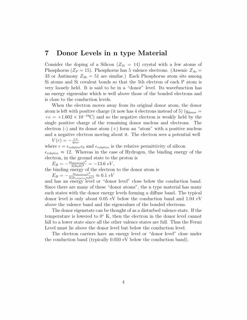
7 Donor Levels in n type Material
Consider the doping of a Silicon (ZSi = 14) crystal with a few atoms ofPhosphorus (ZP = 15). Phosphorus has 5 valence electrons. (Arsenic ZAs =33 or Antimony ZSb = 51 are similar.) Each Phosphorus atom sits amongSi atoms and Si covalent bonds so that the 5th electron of each P atom isvery loosely held. It is said to be in a “donor” level. Its wavefunction hasan energy eigenvalue which is well above those of the bonded electrons andis close to the conduction levels.
When the electron moves away from its original donor atom, the donoratom is left with positive charge (it now has 4 electrons instead of 5) (qdonor =+e = +1.602 × 10⁻¹⁹C) and so the negative electron is weakly held by thesingle positive charge of the remaining donor nucleus and electrons. Theelectron (-) and its donor atom (+) form an “atom” with a positive nucleusand a negative electron moving about it. The electron sees a potential well
V (r) = − e.e4πεr
where ε = εrelativeε0 and εrelative is the relative permittivity of siliconεrelative ≈ 12. Whereas in the case of Hydrogen, the binding energy of theelectron, in the ground state to the proton is
EB = −melectrone4
2(2ε0h)2 = −13.6 eV ,the binding energy of the electron to the donor atom is
EB = − melectrone4
2(2εrelativeε0h)2 ≈ 0.1 eVand has an energy level or “donor level” close below the conduction band.Since there are many of these “donor atoms”, the n type material has manysuch states with the donor energy levels forming a diffuse band. The typicaldonor level is only about 0.05 eV below the conduction band and 1.04 eVabove the valence band and the eigenvalues of the bonded electrons.
The donor eigenstate can be thought of as a disturbed valence state. If thetemperature is lowered to 0◦ K, then the electron in the donor level cannotfall to a lower state since all the other valence states are full. Thus the FermiLevel must lie above the donor level but below the conduction level.
The electron carriers have an energy level or “donor level” close underthe conduction band (typically 0.050 eV below the conduction band).
4
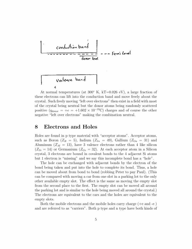
At normal temperatures (at 300◦ K, kT=0.026 eV), a large fraction ofthese electrons can lift into the conduction band and move freely about thecrystal. Such freely moving “left over electrons” then exist in a field with mostof the crystal being neutral but the donor atoms being randomly scatteredpositive (qdonor = +e = +1.602 × 10⁻¹⁹C) charges and of course the othernegative “left over electrons” making the combination neutral.
8 Electrons and Holes
Holes are found in p type material with “acceptor atoms”. Acceptor atoms,such as Boron (ZB = 5), Indium (ZIn = 49), Gallium (ZGa = 31) andAluminum (ZAl = 13), have 3 valence electrons rather than 4 like silicon(ZSi = 14) or Germanium (ZGe = 32). At each acceptor atom in a Siliconcrystal, 3 electrons are bound in covalent bonds to the 4 adjacent Si atomsbut 1 electron is “missing” and we say this incomplete bond has a “hole”.
The hole can be exchanged with adjacent bonds by the electron of thebond being taken and put into the hole to complete its bond. Thus, a holecan be moved about from bond to bond (robbing Peter to pay Paul). (Thiscan be compared with moving a car from one slot in a parking lot to the onlyother available empty slot. The effect is the same as moving the empty slotfrom the second place to the first. The empty slot can be moved all aroundthe parking lot and is similar to the hole being moved all around the crystal.)The electrons are equivalent to the cars and the holes are equivalent to theempty slots.
Both the mobile electrons and the mobile holes carry charge (+e and -e )and are referred to as “carriers”. Both p type and n type have both kinds of
5
carriers but the p type has a majority of hole carriers while the n type has amajority of electron carriers.
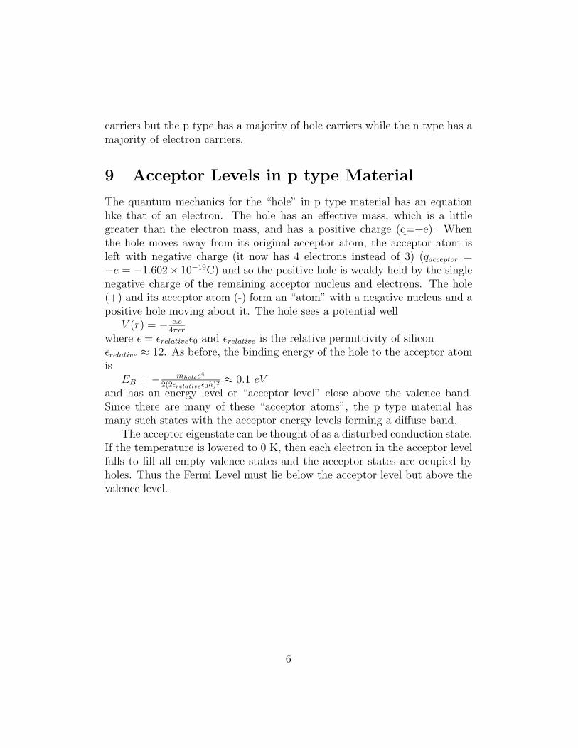
9 Acceptor Levels in p type Material
The quantum mechanics for the “hole” in p type material has an equationlike that of an electron. The hole has an effective mass, which is a littlegreater than the electron mass, and has a positive charge (q=+e). Whenthe hole moves away from its original acceptor atom, the acceptor atom isleft with negative charge (it now has 4 electrons instead of 3) (qacceptor =−e = −1.602× 10⁻¹⁹C) and so the positive hole is weakly held by the singlenegative charge of the remaining acceptor nucleus and electrons. The hole(+) and its acceptor atom (-) form an “atom” with a negative nucleus and apositive hole moving about it. The hole sees a potential well
V (r) = − e.e4πεr
where ε = εrelativeε0 and εrelative is the relative permittivity of siliconεrelative ≈ 12. As before, the binding energy of the hole to the acceptor atomis
EB = − mholee4
2(2εrelativeε0h)2 ≈ 0.1 eVand has an energy level or “acceptor level” close above the valence band.Since there are many of these “acceptor atoms”, the p type material hasmany such states with the acceptor energy levels forming a diffuse band.
The acceptor eigenstate can be thought of as a disturbed conduction state.If the temperature is lowered to 0 K, then each electron in the acceptor levelfalls to fill all empty valence states and the acceptor states are ocupied byholes. Thus the Fermi Level must lie below the acceptor level but above thevalence level.
6
At normal temperatures (at 300◦ K, kT=0.026 eV), a fraction of theseholes can fall into the valence band (ie the electrons lift from Valence toConduction bands) and these holes move freely about the crystal. Such freelymoving “holes” then exist in a field with most of the crystal being neutralbut the acceptor atoms being randomly scattered negative (qacceptor = −e =−1.602×10⁻¹⁹C charges and of course the other positive “holes” making thecombination neutral.
10 Adjacent p and n Type material
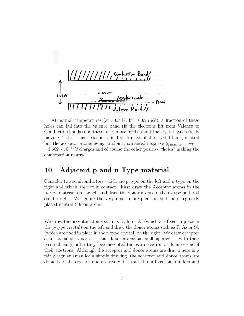
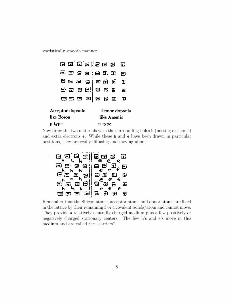
Consider two semiconductors which are p-type on the left and n-type on theright and which are not in contact. First draw the Acceptor atoms in thep-type material on the left and draw the donor atoms in the n-type materialon the right. We ignore the very much more plentiful and more regularlyplaced neutral Silicon atoms.
We draw the acceptor atoms such as B, In or Al (which are fixed in place inthe p-type crystal) on the left and draw the donor atoms such as P, As or Sb(which are fixed in place in the n-type crystal) on the right. We draw acceptoratoms as small squares and donor atoms as small squares with theirresidual charge after they have accepted the extra electron or donated one oftheir electrons. Although the acceptor and donor atoms are drawn here in afairly regular array for a simple drawing, the acceptor and donor atoms aredopants of the crystals and are really distributed in a fixed but random and
7
statistically smooth manner
Now draw the two materials with the surrounding holes h (missing electrons)and extra electrons e. While these h and e have been drawn in particularpositions, they are really diffusing and moving about.
Remember that the Silicon atoms, acceptor atoms and donor atoms are fixedin the lattice by their remaining 3 or 4 covalent bonds/atom and cannot move.They provide a relatively neutrally charged medium plus a few positively ornegatively charged stationary centers. The few h’s and e’s move in thismedium and are called the “carriers”.
8
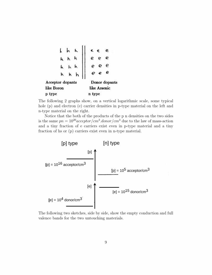
The following 2 graphs show, on a vertical logarithmic scale, some typicalhole (p) and electron (e) carrier densities in p-type material on the left andn-type material on the right.
Notice that the both of the products of the p n densities on the two sidesis the same pn = 1020acceptor/cm3.donor/cm3 due to the law of mass-actionand a tiny fraction of e carriers exist even in p-type material and a tinyfraction of hs or (p) carriers exist even in n-type material.
[p] type [n] type
[�p] = 1016 acceptor/cm3
[�p] = 105 acceptor/cm3
[�p]
[�e]
[�e] = 104 donor/cm3
[�e] = 1015 donor/cm3
The following two sketches, side by side, show the empty conduction and fullvalence bands for the two untouching materials.
9
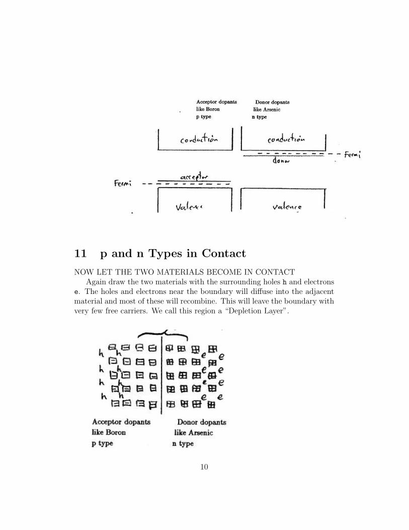
11 p and n Types in Contact
NOW LET THE TWO MATERIALS BECOME IN CONTACTAgain draw the two materials with the surrounding holes h and electrons
e. The holes and electrons near the boundary will diffuse into the adjacentmaterial and most of these will recombine. This will leave the boundary withvery few free carriers. We call this region a “Depletion Layer”.
10
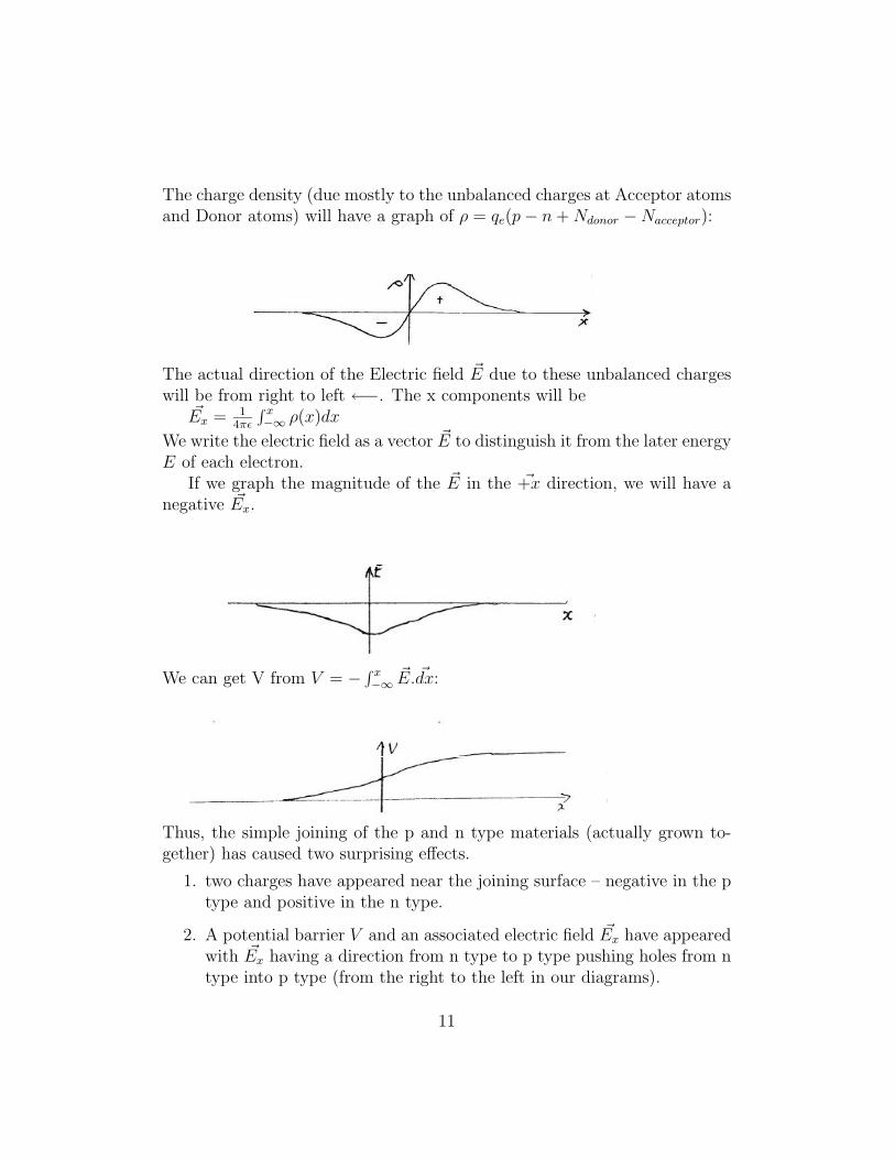
The charge density (due mostly to the unbalanced charges at Acceptor atomsand Donor atoms) will have a graph of ρ = qe(p− n+Ndonor −Nacceptor):
The actual direction of the Electric field ~E due to these unbalanced chargeswill be from right to left ←−. The x components will be
~Ex = 14πε
∫ x−∞ ρ(x)dx
We write the electric field as a vector ~E to distinguish it from the later energyE of each electron.
If we graph the magnitude of the ~E in the ~+x direction, we will have anegative ~Ex.
We can get V from V = −∫ x−∞
~E. ~dx:
Thus, the simple joining of the p and n type materials (actually grown to-gether) has caused two surprising effects.
1. two charges have appeared near the joining surface – negative in the ptype and positive in the n type.
2. A potential barrier V and an associated electric field ~Ex have appearedwith ~Ex having a direction from n type to p type pushing holes from ntype into p type (from the right to the left in our diagrams).
11
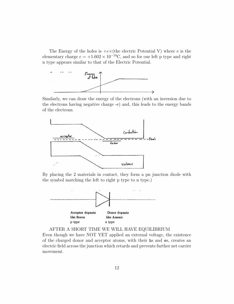
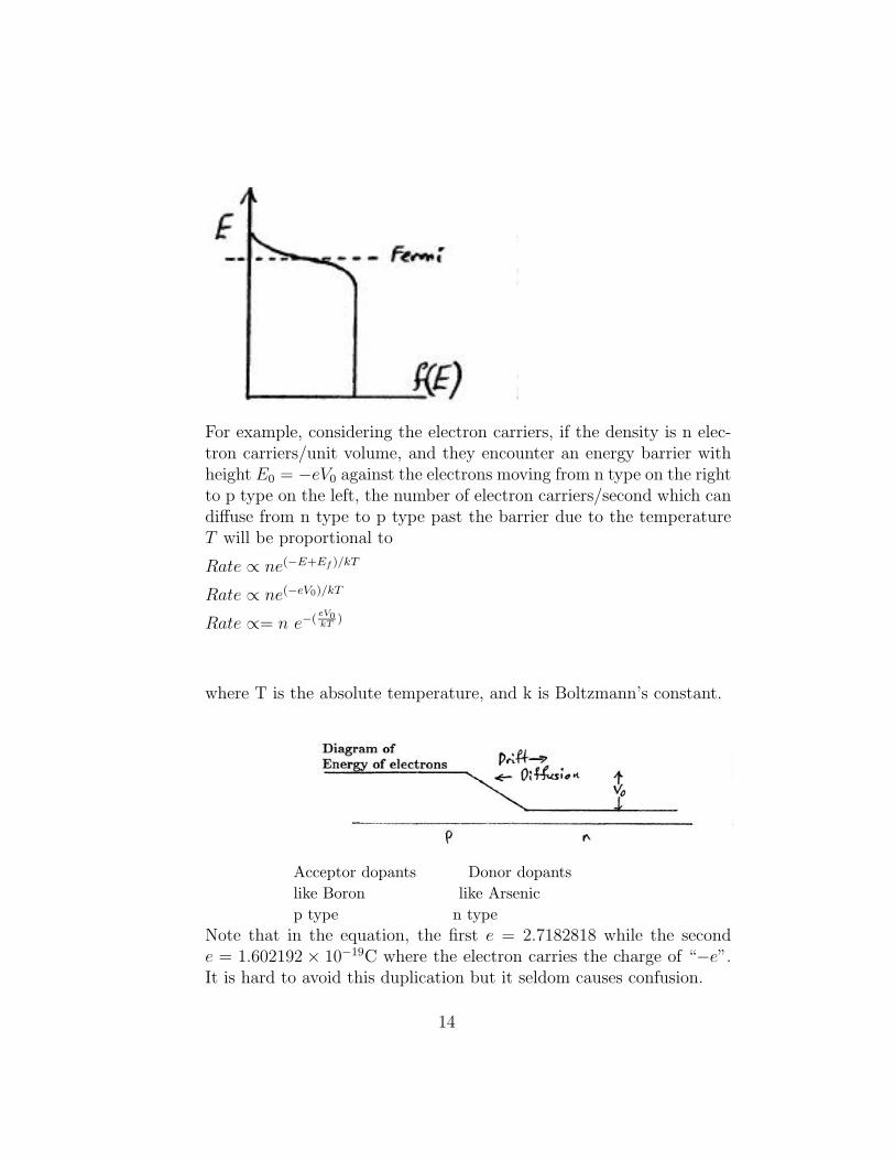
The Energy of the holes is +e×(the electric Potential V) where e is theelementary charge e = +1.602× 10⁻¹⁹C, and so for our left p type and rightn type appears similar to that of the Electric Potential.
Similarly, we can draw the energy of the electrons (with an inversion due tothe electrons having negative charge -e) and, this leads to the energy bandsof the electrons.
By placing the 2 materials in contact, they form a pn junction diode withthe symbol matching the left to right p type to n type.)
AFTER A SHORT TIME WE WILL HAVE EQUILIBRIUMEven though we have NOT YET applied an external voltage, the existenceof the charged donor and acceptor atoms, with their hs and es, creates anelectric field across the junction which retards and prevents further net carriermovement.
12
On both sides of the junction we will have a region which is nearly empty ofcarriers. This is called the Depletion Region.
Actually, of course, the carriers still move a little but the net movementbecomes zero.
We define two kinds of origins for electron movement.
1. Drift = movement due to Electric Field
The movement is not infinite because the electrons are scattered es-pecially when as each electron accelerates, the de Broglie λ = h
pof
the electron momentum becomes comparable with the atomic diame-ter and the electron is likely to be scattered. Thus the x component ofits velocity rises as it accelerates then falls to zero and the accelerationstarts over again. Thus the average speed of the electron is limited.
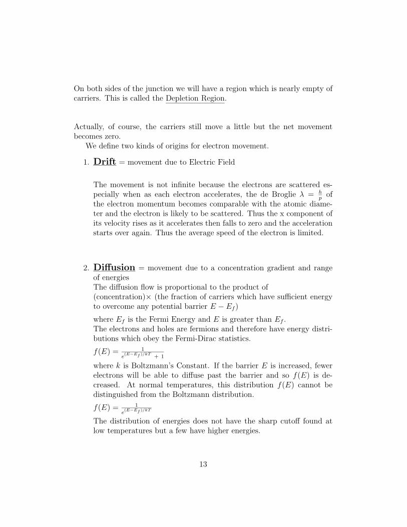
2. Diffusion = movement due to a concentration gradient and rangeof energiesThe diffusion flow is proportional to the product of(concentration)× (the fraction of carriers which have sufficient energyto overcome any potential barrier E − Ef )where Ef is the Fermi Energy and E is greater than Ef .The electrons and holes are fermions and therefore have energy distri-butions which obey the Fermi-Dirac statistics.
f(E) = 1
e(E−Ef )/kT
+ 1
where k is Boltzmann’s Constant. If the barrier E is increased, fewerelectrons will be able to diffuse past the barrier and so f(E) is de-creased. At normal temperatures, this distribution f(E) cannot bedistinguished from the Boltzmann distribution.
f(E) = 1
e(E−Ef )/kT
The distribution of energies does not have the sharp cutoff found atlow temperatures but a few have higher energies.
13
For example, considering the electron carriers, if the density is n elec-tron carriers/unit volume, and they encounter an energy barrier withheight E0 = −eV0 against the electrons moving from n type on the rightto p type on the left, the number of electron carriers/second which candiffuse from n type to p type past the barrier due to the temperatureT will be proportional to
Rate ∝ ne(−E+Ef )/kT
Rate ∝ ne(−eV0)/kT
Rate ∝= n e−(eV0kT
)
where T is the absolute temperature, and k is Boltzmann’s constant.
Acceptor dopants Donor dopantslike Boron like Arsenicp type n type
Note that in the equation, the first e = 2.7182818 while the seconde = 1.602192 × 10⁻¹⁹C where the electron carries the charge of “−e”.It is hard to avoid this duplication but it seldom causes confusion.
14
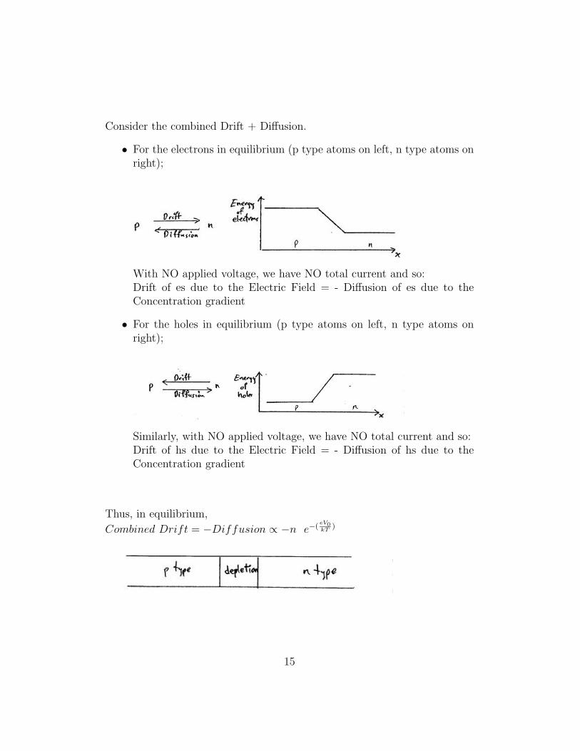
Consider the combined Drift + Diffusion.
• For the electrons in equilibrium (p type atoms on left, n type atoms onright);
With NO applied voltage, we have NO total current and so:Drift of es due to the Electric Field = - Diffusion of es due to theConcentration gradient
• For the holes in equilibrium (p type atoms on left, n type atoms onright);
Similarly, with NO applied voltage, we have NO total current and so:Drift of hs due to the Electric Field = - Diffusion of hs due to theConcentration gradient
Thus, in equilibrium,
Combined Drift = −Diffusion ∝ −n e−(eV0kT
)
15
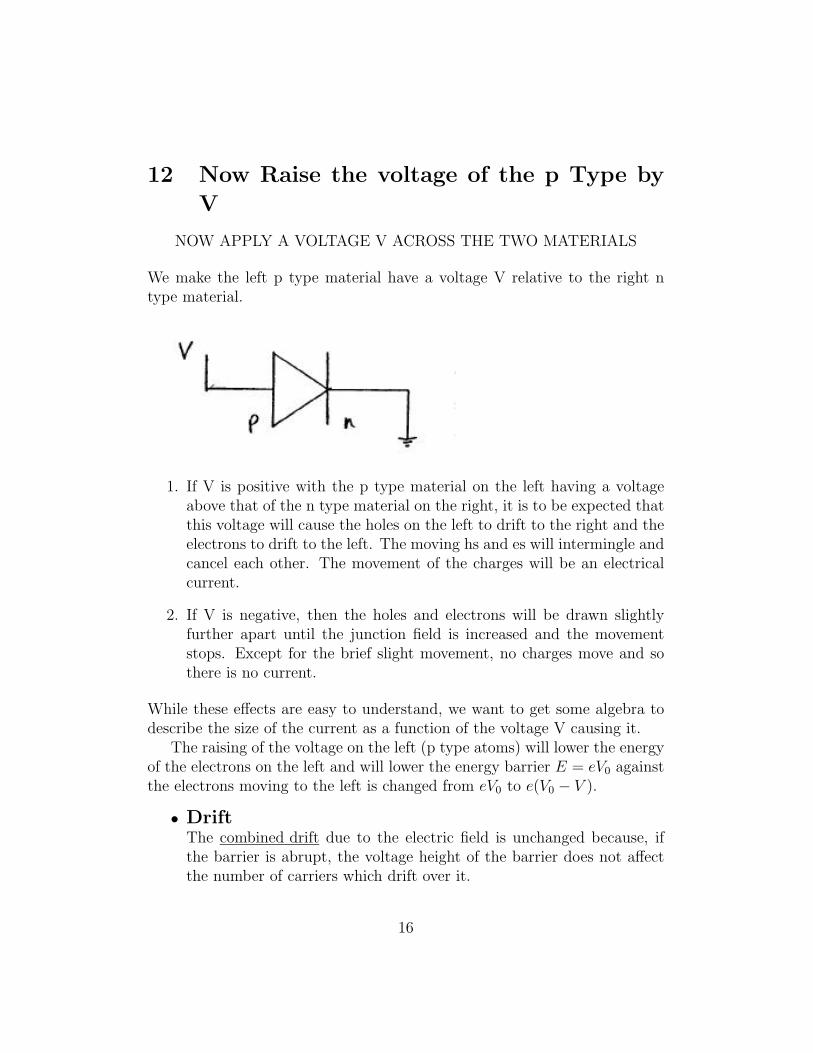
12 Now Raise the voltage of the p Type by
V
NOW APPLY A VOLTAGE V ACROSS THE TWO MATERIALS
We make the left p type material have a voltage V relative to the right ntype material.
1. If V is positive with the p type material on the left having a voltageabove that of the n type material on the right, it is to be expected thatthis voltage will cause the holes on the left to drift to the right and theelectrons to drift to the left. The moving hs and es will intermingle andcancel each other. The movement of the charges will be an electricalcurrent.
2. If V is negative, then the holes and electrons will be drawn slightlyfurther apart until the junction field is increased and the movementstops. Except for the brief slight movement, no charges move and sothere is no current.
While these effects are easy to understand, we want to get some algebra todescribe the size of the current as a function of the voltage V causing it.
The raising of the voltage on the left (p type atoms) will lower the energyof the electrons on the left and will lower the energy barrier E = eV0 againstthe electrons moving to the left is changed from eV0 to e(V0 − V ).
• DriftThe combined drift due to the electric field is unchanged because, ifthe barrier is abrupt, the voltage height of the barrier does not affectthe number of carriers which drift over it.
16
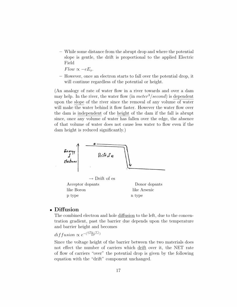
– While some distance from the abrupt drop and where the potentialslope is gentle, the drift is proportional to the applied ElectricField
Flow ∝ −eEx.– However, once an electron starts to fall over the potential drop, it
will continue regardless of the potential or height.
(An analogy of rate of water flow in a river towards and over a dammay help. In the river, the water flow (in meter3/second) is dependentupon the slope of the river since the removal of any volume of waterwill make the water behind it flow faster. However the water flow overthe dam is independent of the height of the dam if the fall is abruptsince, once any volume of water has fallen over the edge, the absenceof that volume of water does not cause less water to flow even if thedam height is reduced significantly.)
→ Drift of esAcceptor dopants Donor dopantslike Boron like Arsenicp type n type
• DiffusionThe combined electron and hole diffusion to the left, due to the concen-tration gradient, past the barrier due depends upon the temperatureand barrier height and becomes
diffusion ∝ e−(e(V0−V )
kT)
Since the voltage height of the barrier between the two materials doesnot effect the number of carriers which drift over it, the NET rateof flow of carriers “over” the potential drop is given by the followingequation with the “drift” component unchanged.
17
Net F low ∝ [diffusion+ drift]
Net F low ∝ [e−(e(V0−V )
kT) − e−(
eV0kT
)]
Net F low ∝ e−(eV0kT
)[e( eVkT
) − 1]
The resulting current is
I ∝ e× (NET Flow)
I ∝ e× e−(eV0kT
)[e( eVkT
) − 1]
We combine the proportionality constant, the value of the elementarycharge e = 1.602× 10⁻¹⁹C on each electron and hole and the first term
e−(eV0kT
) into a constant “saturation current” Is ∝ e × e−eV0kT to get the
electric current
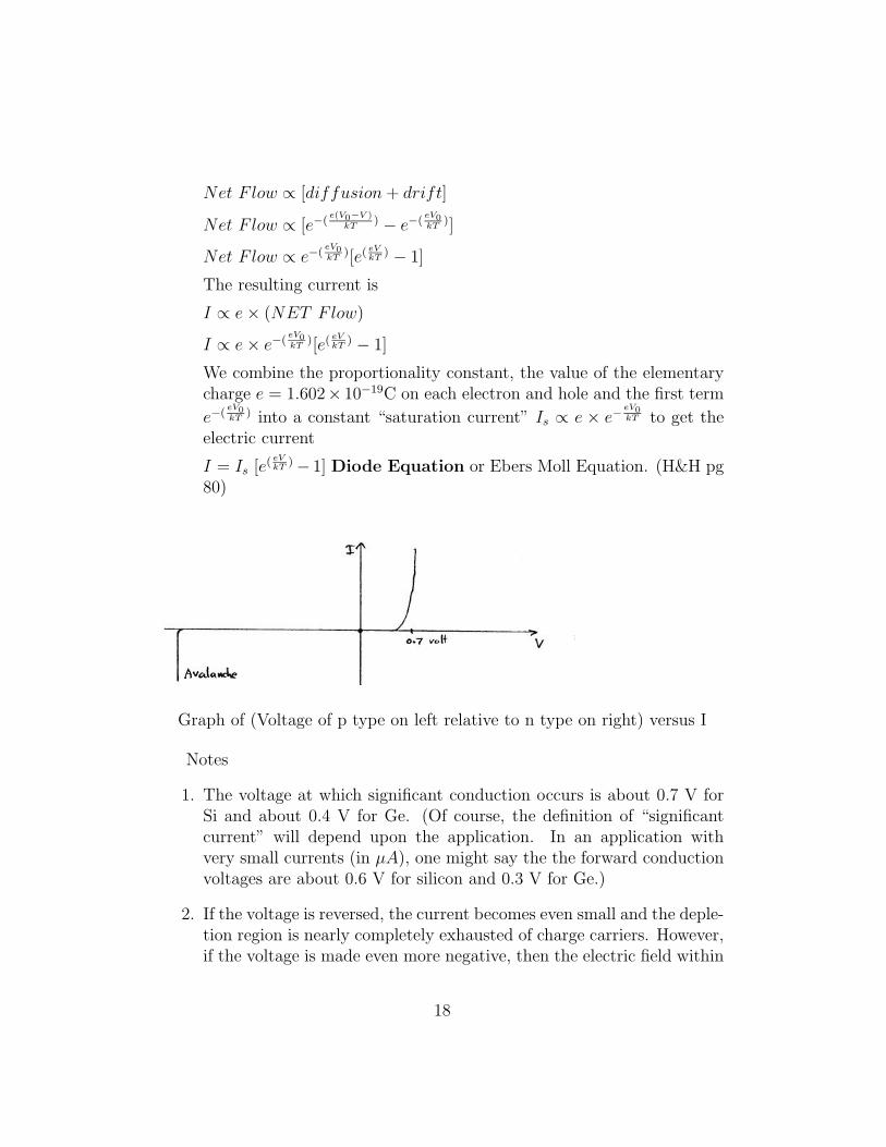
I = Is [e( eVkT
)− 1] Diode Equation or Ebers Moll Equation. (H&H pg80)
Graph of (Voltage of p type on left relative to n type on right) versus I
Notes
1. The voltage at which significant conduction occurs is about 0.7 V forSi and about 0.4 V for Ge. (Of course, the definition of “significantcurrent” will depend upon the application. In an application withvery small currents (in µA), one might say the the forward conductionvoltages are about 0.6 V for silicon and 0.3 V for Ge.)
2. If the voltage is reversed, the current becomes even small and the deple-tion region is nearly completely exhausted of charge carriers. However,if the voltage is made even more negative, then the electric field within
18
the narrow depletion zone can become sufficiently high for avalancheeffects to occur. In an avalanche, a stray electron (perhaps producedby the ionization trail of a cosmic ray can accelerate so rapidly thatit may not be scattered when its de Broglie wavelength is comparablewith a nearby atomic potential well and it may gain enough energythat, when it eventually hits an atom, it may ionize the atom. The 1electron may cause 2 loose electrons which, in turn, cause many more.Thus at a critical large reverse bias, the current may increase suddenly.This effect is used in Zener Diodes.
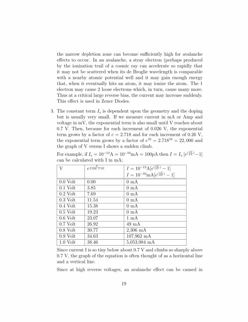
3. The constant term Is is dependent upon the geometry and the dopingbut is usually very small. If we measure current in mA or Amp andvoltage in mV, the exponential term is also small until V reaches about0.7 V. Then, because for each increment of 0.026 V, the exponentialterm grows by a factor of e = 2.718 and for each increment of 0.26 V,the exponential term grows by a factor of e10 = 2.71810 = 22, 000 andthe graph of V versus I shows a sudden climb.
For example, if Is = 10−13A = 10−10mA = 100pA then I = Is [e( eVkT
)−1]can be calculated with I in mA;
V eV
0.026 V olt I = 10−13A[e( eVkT
) − 1]
I = 10−10mA[e( eVkT
) − 1]
0.0 Volt 0.00 0 mA0.1 Volt 3.85 0 mA0.2 Volt 7.69 0 mA0.3 Volt 11.54 0 mA0.4 Volt 15.38 0 mA0.5 Volt 19.23 0 mA0.6 Volt 23.07 1 mA0.7 Volt 26.92 49 mA0.8 Volt 30.77 2,306 mA0.9 Volt 34.63 107,962 mA1.0 Volt 38.46 5,053,984 mA
Since current I is so tiny below about 0.7 V and climbs so sharply above0.7 V, the graph of the equation is often thought of as a horizontal lineand a vertical line.
Since at high reverse voltages, an avalanche effect can be caused in
19
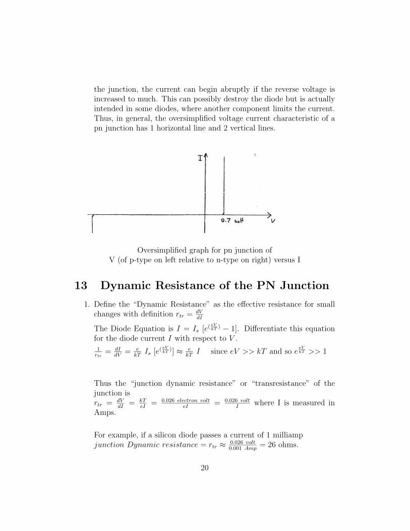
the junction, the current can begin abruptly if the reverse voltage isincreased to much. This can possibly destroy the diode but is actuallyintended in some diodes, where another component limits the current.Thus, in general, the oversimplified voltage current characteristic of apn junction has 1 horizontal line and 2 vertical lines.
Oversimplified graph for pn junction ofV (of p-type on left relative to n-type on right) versus I
13 Dynamic Resistance of the PN Junction
1. Define the “Dynamic Resistance” as the effective resistance for smallchanges with definition rtr = dV
dI
The Diode Equation is I = Is [e( eVkT
) − 1]. Differentiate this equationfor the diode current I with respect to V .1rtr
= dIdV
= ekT
Is [e( eVkT
)] ≈ ekT
I since eV >> kT and so eeVkT >> 1
Thus the “junction dynamic resistance” or “transresistance” of thejunction isrtr = dV
dI= kT
eI= 0.026 electron volt
eI= 0.026 volt
Iwhere I is measured in
Amps.
For example, if a silicon diode passes a current of 1 milliampjunction Dynamic resistance = rtr ≈ 0.026 volt
0.001 Amp= 26 ohms.
20
2. In addition, the materials add a little ohmic resistance as well, typicallyabout 2 ohm (depending upon the physical size of the material).
Thus the total dynamic resistance of a Silicon diode is typically aboutRdynamic = rtr = dV
dI= 2 ohm+ 0.026 volt
I
orRdynamic = rtr = dV
dI= 2 ohm+ 0.026 ohm/Amp
I
[This is sometimes expressed poorly (please do not do this)with inconsistent units as Rdynamic = dV
dI= 2 ohm+ 26
ImA]
The added 2 ohms is typical but will vary from diode to diode dependingupon the diode width and construction.
For example, if I = 10 mA, thenRdynamic = rtr = 2 ohm+ 0.026 ohm/Amp
0.010 Amp
Rdynamic = rtr = (2 + 2.6) ohm = 4.6 ohms.
21
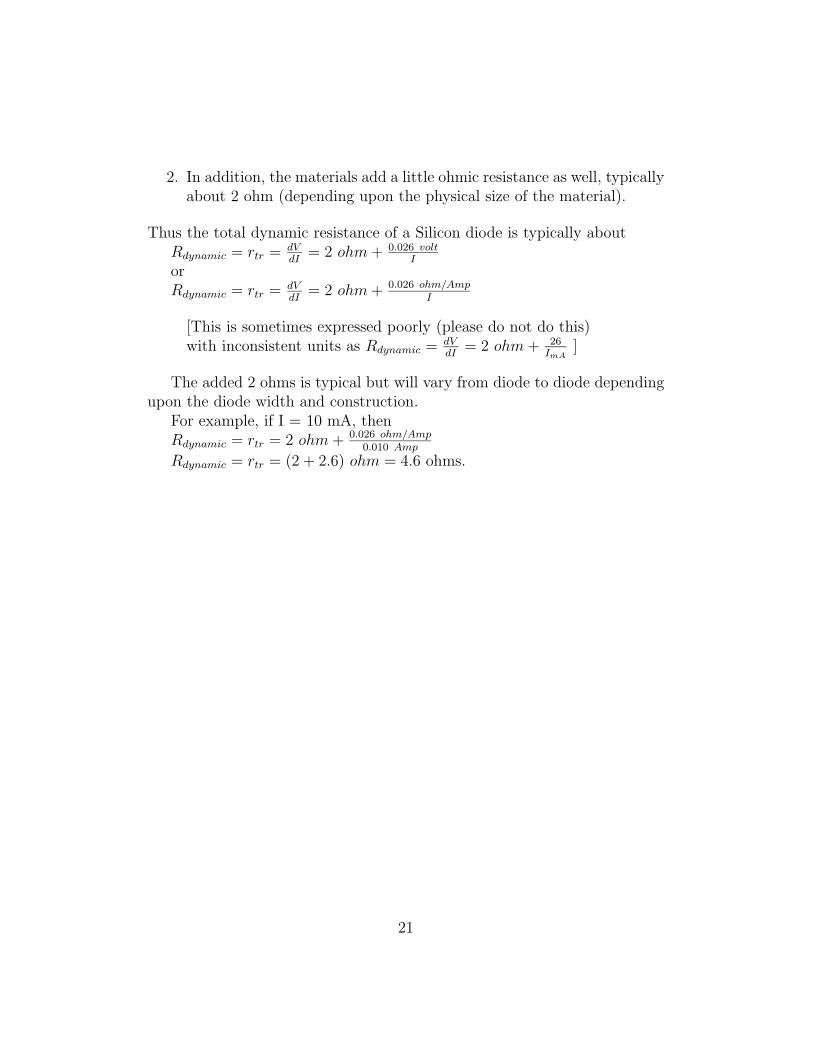
14 Energy Levels in Junctions
1. Unbiased Junction (no voltage applied)(p type with acceptor impurity atoms on left and n type with donorimpurity atoms on right)
Acceptor dopants Donor dopantslike Boron like Arsenicp type n type
• This is not drawn to scale!
• The band gap is about 1.09 eV to 1.12 eV for Silicon
• The ionized acceptor states are only about 0.05 eV above thevalence band.
• the Fermi level is only about 0.025 eV above the valence band.
22
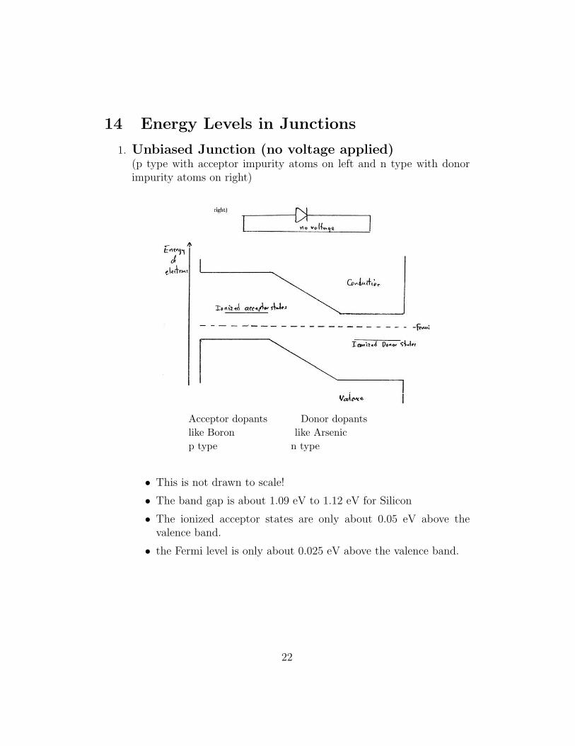
2. Forward-Biased Junction(Positive voltage applied to p type material on left). (p type withacceptor impurity atoms on left and n type with donor impurity atomson right)
Acceptor dopants Donor dopantslike Boron like Arsenicp type n type
• When forward biased, many of both kinds of mobile carriers aredrawn into the junction region eliminating the charge depletion.The holes are not filled immediately by electrons and we say theregion has a storage charge.
23
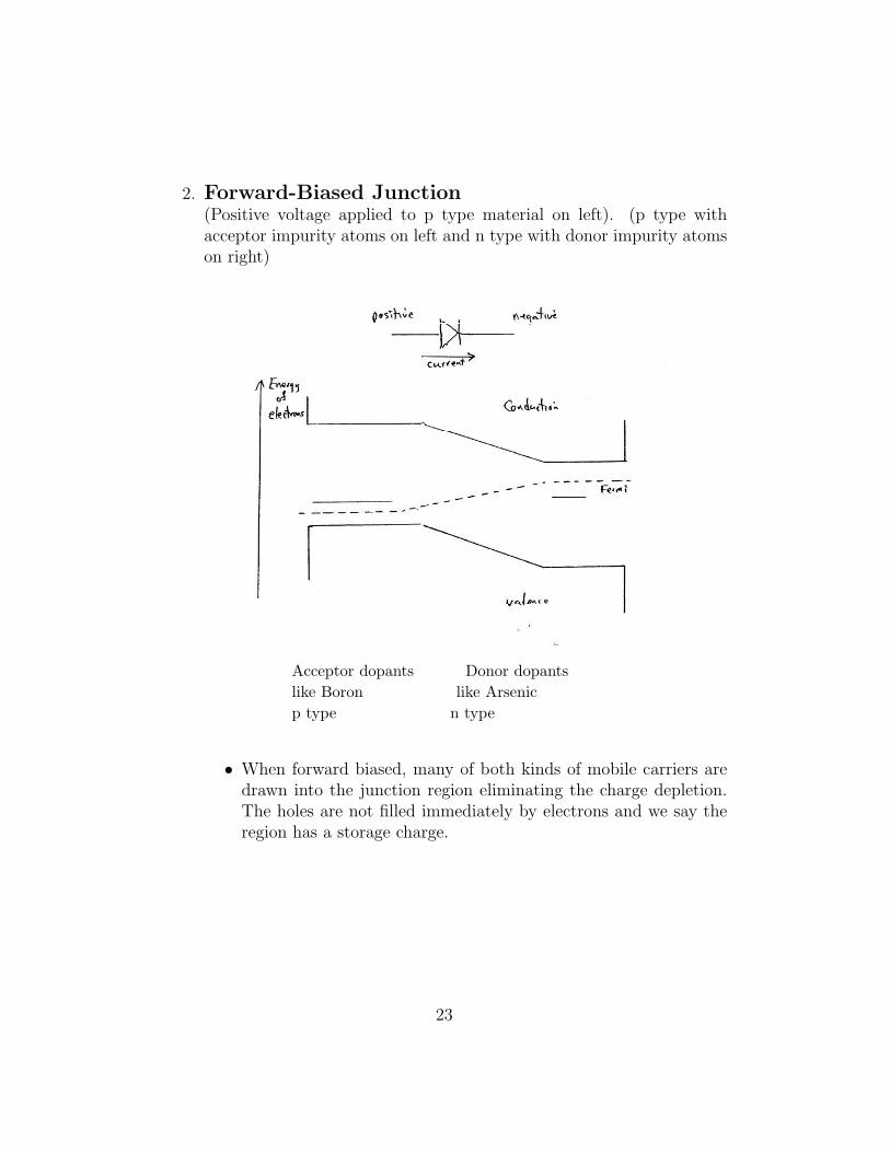
3. Back-Biased Junction(Negative voltage applied to p type material) (p type on left and n typeon right)
Acceptor dopants Donor dopantslike Boron like Arsenicp type n type
• When back biased, all mobile carriers are drawn away from thejunction region causing a wider charge depletion region.
24
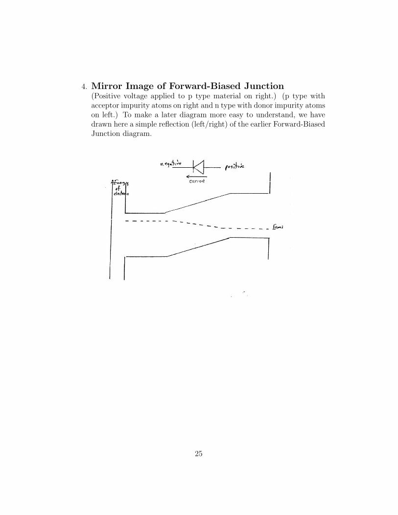
4. Mirror Image of Forward-Biased Junction(Positive voltage applied to p type material on right.) (p type withacceptor impurity atoms on right and n type with donor impurity atomson left.) To make a later diagram more easy to understand, we havedrawn here a simple reflection (left/right) of the earlier Forward-BiasedJunction diagram.
25
15 Two pn Junctions
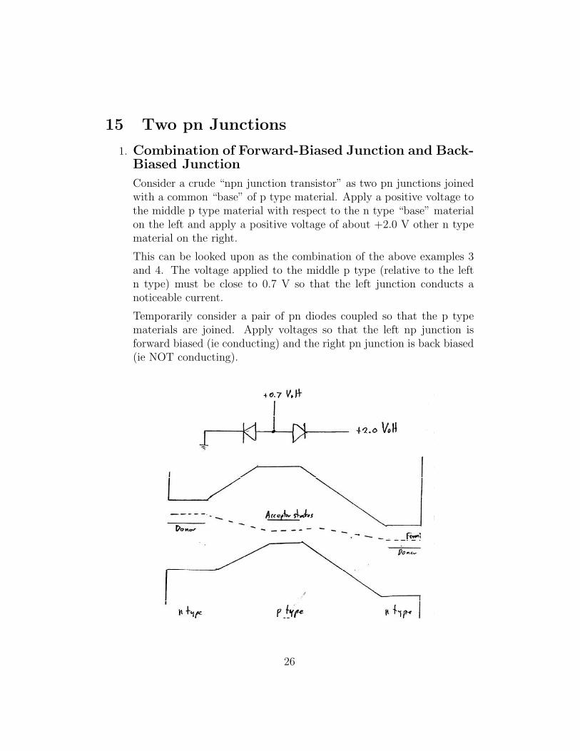
1. Combination of Forward-Biased Junction and Back-Biased Junction
Consider a crude “npn junction transistor” as two pn junctions joinedwith a common “base” of p type material. Apply a positive voltage tothe middle p type material with respect to the n type “base” materialon the left and apply a positive voltage of about +2.0 V other n typematerial on the right.
This can be looked upon as the combination of the above examples 3and 4. The voltage applied to the middle p type (relative to the leftn type) must be close to 0.7 V so that the left junction conducts anoticeable current.
Temporarily consider a pair of pn diodes coupled so that the p typematerials are joined. Apply voltages so that the left np junction isforward biased (ie conducting) and the right pn junction is back biased(ie NOT conducting).
26
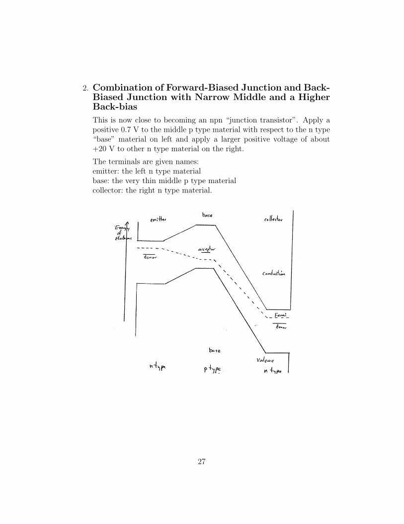
2. Combination of Forward-Biased Junction and Back-Biased Junction with Narrow Middle and a HigherBack-bias
This is now close to becoming an npn “junction transistor”. Apply apositive 0.7 V to the middle p type material with respect to the n type“base” material on left and apply a larger positive voltage of about+20 V to other n type material on the right.
The terminals are given names:emitter: the left n type materialbase: the very thin middle p type materialcollector: the right n type material.
27
16 An npn Junction Transistor
A real npn junction transistor has a very thin base so that electrons leavingthe emitter and travelling into the base immediately “feel” the strong elec-tric field ~E of the back-biassed junction and can fall “downhill towards thecollector”.
By making the base thin, the chance of the electrons meeting a free holein the p type base before being swept away by the collector’s field can bereduced to about 2% in spite of the high concentration of holes in the p typebase. In other words, if a current i leaves the emitter, then only about 0.02 ileaves the base wire and about 0.98 i leaves the collector.
The fraction which leaves the base wire is called α.α = ibase
iemitter
In this example α = 0.981.0
= 0.98The ratio of the current which leaves the collector to that which leaves theemitter is called β.
β = icollectoribase
In this example, β = 0.980.02≈ 49.0
28