Online Education Group 7 Hou Xingwu Liu Jianwei Yan Weitao Wan Peng.

www.MaterialsViews.comwww.advopticalmat.de
FULL P
APER
Guowei Xu,* Jianwei Liu, Qian Wang, Rongqing Hui, Zhijun Chen, Victor A. Maroni, and Judy Wu
Plasmonic Graphene Transparent Conductors
Plasmonic graphene is fabricated using thermally assisted self-assembly of silver nanoparticles on graphene. The localized surface-plasmonic effect is demonstrated with the resonance frequency shifting from 446 to 495 nm when the lateral dimension of the Ag nanoparticles increases from about 50 to 150 nm. Finite-difference time-domain simulations are employed to con-firm the experimentally observed light-scattering enhancement in the solar spectrum in plasmonic graphene and the decrease of both the plasmonic resonance frequency and amplitude with increasing graphene thickness. In addition, plasmonic graphene shows much-improved electrical conductance by a factor of 2–4 as compared to the original graphene, making the plas-monic graphene a promising advanced transparent conductor with enhanced light scattering for thin-film optoelectronic devices.
1. Introduction
Graphene, a single layer of carbon atoms arranged in a hex-agonal lattice,[1,2] has the unique properties of a high carrier mobility, high optical transmittance, chemical inertness, and flexibility, making it attractive for optoelectronic applications.[2] In particular, graphene may provide a promising alternative to indium tin oxide (ITO) as a transparent conductor (TC).[2] Currently, ITO is widely employed as a transparent conduc-tive electrode with a sheet resistance of 10–30 Ω square−1 and a transparency of 90% at 550 nm wavelength (λ).[1] However, long-term use of ITO has severe limitations. It is scarce and consequently becomes prohibitively expensive as the massive demand for photovoltaic devices increases. In addition, ITO is brittle and has a much-reduced transparency at longer wave-lengths, which are unfavorable for high-efficiency, broad-band photovoltaic devices on flexible substrates. Graphene has several unique advantages as a TC for photovoltaics such as its high
© 2012 WILEY-VCH Verlag GmbH & Co. KGaA, Weinheim
G. Xu, Dr. J. Liu, Prof. J. Wu Department of Physics & Astronomy University of Kansas Lawrence, KS 66045, USA E-mail: [email protected]. Wang, Prof. R. Hui Department of Engineering & Computer Science University of Kansas, Lawrence, KS 66045, USADr. Z. Chen, Dr. V. A. MaroniMaterials Science Division, Bldg 212 Argonne National Laboratory Argonne, IL 60439, USA
DOI: 10.1002/adma.201104846
Adv. Mater. 2012, 24, OP71–OP76
electrical conductivity, remarkable optical transparency, and favorable work function of ∼4.42 eV.[3,4] Graphene absorbs only about 2.3% of the incident white light due to its unique gapless electronic structure. In particular, the recent work on large-area growth of graphene using chemical vapor deposition (CVD) on metal foils has made a critical step toward the application of graphene for flexible TCs.[1,5] Further development of a graphene-based TC is therefore important to high-performance and low-cost photovoltaics and other opto-electronic devices.
In thin-film solar cells, plasmonic struc-tures that promote the collective oscillation of electrons at a resonance frequency at
the interface of metals and dielectric materials, have been dem-onstrated as effective in enhancing light scattering and hence light absorption.[6] Exciting progress has been made recently in the application of plasmonics in thin-film solar cells,[6] espe-cially in Si-based[7] and organic solar cells.[8] One approach to integrate plasmonics into solar cells is through the addition of metal nanoparticles (NPs), on which the resonance frequency of the localized surface plasmons is primarily determined by the charge-carrier density of the metal and can be further tuned by the size, shape, and surrounding dielectric medium of metal NPs.[9] A variety of metals have been investigated and Ag seems to be a favorable one due to its plasmonic frequency in the vis-ible range and low Ohmic losses. Enhanced light trapping has yielded increased photocurrents in solar cells with plasmonic structures implemented.[10,11] Most recently, graphene with plasmonic nanostructures was reported to strongly enhance the efficiency of graphene-based photodetectors.[12] Development of plasmonic graphene is hence of primary importance to its appli-cation in advanced TCs for optoelectronic devices. In this work, we report the fabrication of plasmonic graphene by depositing Ag NPs onto CVD-grown graphene using a thermally assisted self-assembly method. Characterization of the localized surface-plasmonic effect was carried out using Raman spectroscopy in combination with visible optical spectroscopy using an inte-grating sphere. Simulation using the finite-difference time-domain (FDTD) method was employed to understand the effect of graphene thickness on the plasmonic effect.
2. Results and Discussion
Figure 1 depicts the scanning electron microscopy (SEM) images of the plasmonic graphene made from the original Ag
OP71wileyonlinelibrary.com

OP72
www.MaterialsViews.comwww.advopticalmat.de
FULL
PAPER
Figure 1. CVD Graphene transferred on a Si substrate and decorated with Ag NPs formed through thermal annealing Ag films of thickness of, respectively, a) 4 nm; b) 8 nm; and c) 14 nm evaporated on graphene.
films with thicknesses of 4, 8, and 14 nm. A uniform distribu-tion of the Ag NPs self-assembled on graphene was obtained after the thermal annealing. The size and shape of the Ag NPs were found to be dependent on the thickness of the original Ag film. At thicknesses of 4 and 8 nm, circular Ag NPs formed after the thermal annealing with average diameters of about 50 and 70 nm, respectively, as shown in Figure 1a and b. At a larger thickness of 14 nm, elongated and irregularly shaped Ag NPs appeared with average dimensions of ∼150 nm. A study using atomic force microscopy (AFM) revealed that both the lateral and vertical dimensions of the Ag NPs increase with increasing thickness of the Ag film. The average heights of Ag NPs are 12, 18, and 57 nm, respectively, for the three samples shown in Figures 1a–c. Therefore, by simply tuning the thickness of the Ag film, the size, the shape of the Ag NPs on graphene can be varied. It is worth pointing out that, under the same processing conditions, the Ag NPs formed on the dielectric surfaces show smaller average lateral dimensions as compared to those on graphene (Table 1), possibly due to the difference in the inter-faces. The influence of the interface on the metal NP dimension has been previously reported. For example, the average lateral dimensions of 136, 124, and 128 nm were observed for Ag NPs formed on glass, Si3N4, and TiO2, respectively, by annealing 14 nm-thick Ag film.[10]
Localized surface plasmons are confined collective oscilla-tions of the free electrons in metal NPs. Upon excitation with incident light, the collective motion of the free electrons results in a buildup of polarization charges on the surface of metal NPs, which acts as a restoring force for the resonance occurrence
© 2012 WILEY-VCH Verlag Gmwileyonlinelibrary.com
Table 1. Lateral dimensions of Ag NPs formed through thermal annealing from Ag films of different thicknesses on SiO2 and graphene/SiO2.
Original Ag film thickness [nm]
Ag NPs on glass [nm]a)
Ag NPs on graphene [nm]a)
4 42.0 ± 4.7 49.3 ± 7.7
8 59.9 ± 8.7 67.5 ± 14.1
14 140.4 ± 42.1 147.5 ± 35.7
a)Values are lateral dimension ± standard deviation
at the surface plasmonic frequency.[9] In the region of surface plasmonic resonance frequency (or wavelength λ), the incident light is strongly scattered or absorbed. As stated earlier, such a frequency is determined primarily by the charge-carrier density of metal NPs and can be tuned across a moderate range by the size, shape, and surrounding medium of metal NPs. In general, NPs with larger lateral dimensions tend to have more redshifted frequencies. Figure 2a plots the optical transmittance versus wavelength curves for Ag NPs of various dimensions on both the graphene/glass and bare glass substrates, measured with an integrating sphere. For comparison, the transmittance for original graphene is also included, which is above 90% across almost the entire visible range and over 97% at wavelengths above 550 nm. In contrast, a dip in the transmittance curve appears on all other curves taken on glass and graphene/glass decorated with Ag NPs, suggesting the presence of the localized surface plasmonic resonance near the resonance frequencies at the dips. The resonance dip becomes shallower, broader, and redshifted when the lateral dimension of the Ag NPs increases. Specifically, the resonance wavelengths are 440, 452, and 478 nm for 4, 8, and 14 nm Ag NPs on bare glass, respectively. This result is comparable to that reported earlier by Beck et al. on similar samples in terms of both the plasmonic resonance frequency and the magnitude of transmission.[10] The transmit-tance curves for plasmonic graphene samples show a similar trend with the slightly redshifted plasmonic resonance frequen-cies of 446, 460, and 495 nm for Ag NPs annealed from 4, 8, and 14 nm Ag films on graphene, respectively. Such redshifted plasmonic frequencies can be attributed to combined effect of the increased size of the Ag NPs (Table 1) and the refractive index of the surrounding medium (ng = 2.4[13] for graphene, higher than np = 1.5 for pyrex glass), which is consistent with the previous report that higher refractive indices in the sub-strate would result in longer resonance wavelengths.[14] Com-pared to the Ag NPs-on-glass case, the plasmonic resonance of Ag NPs on graphene is dampened to some extent when the graphene layer is added between the Ag NPs and the glass sub-strate. This variation may be attributed primarily to the energy transfer from Ag NPs to graphene, which dissipates the elec-trical-field concentration on the surface of the Ag NPs. To con-firm this, transmittance spectra of plasmonic graphene with different layers of graphene were taken, shown in Figure 2b,
bH & Co. KGaA, Weinheim Adv. Mater. 2012, 24, OP71–OP76

www.MaterialsViews.comwww.advopticalmat.de
FULL P
APER
Figure 2. a) Transmittance spectra taken on original graphene (black) and plasmonic graphene on glass substrates (colored solid lines) showing a redshift of the surface plasmonic reso-nance frequency with increasing thickness of the Ag film (or increasing lateral size of the Ag NPs); the transmittance spectra of Ag NPs on glass substrates (colored dashed lines) made in the same runs with the corresponding plasmonic graphene are also included for comparison. b) Transmittance spectra of 4 nm Ag NPs on bare glass and graphene of 1, 2, and 3 layers on glass. c) Plasmonic resonance frequency and amplitude with respect to the number of graphene layers. d) Simulated Q-values of Ag disks with 10 nm thickness and 40 nm diameter without graphene (open circles), with a 0.7 nm graphene layer (open squares), and with a 2 nm graphene layer (stars) between the Ag disk and the glass substrate.
which indicate a dependence of the plasmonic resonance of plasmonic graphene on the number of layers of graphene. Indeed, compared to Ag NPs on bare glass, the plasmonic reso-nance of Ag NPs on graphene damps with increasing layers of graphene, shown in Figure 2c. Therefore, multilayer graphene,
© 2012 WILEY-VCH Verlag GmbH & Co. KGaA, Wein
Figure 3. Simulated field distributions measured with monitors placed at different locations and directions: b) simulation configuration; distribution of optical field in the yz plane at a) x = –5 nm, c) x = 5 nm and in the horizontal xy plane at d) inside Ag NP with z = 10 nm, e) inside the graphene layer with z = 15 nm, and f) inside the substrate with z = 20 nm.
Adv. Mater. 2012, 24, OP71–OP76
which possesses better conductivity,[15] facili-tates the energy transfer from Ag NPs to graphene, thus dissipating the localized elec-trical-field concentration on the surface of the Ag NPs, resulting in a decrease of the ampli-tude of their plasmonic resonance. It is worth pointing out that the plasmonic resonance frequency redshifts with increasing layers of graphene, from 420 nm for Ag NPs on bare glass to 440 nm on 3-layer graphene, as indi-cated in Figure 2c. There is a slight difference in the plasmonic resonance frequencies for 4 nm Ag NPs shown in Figure 2a and b, which is most probably caused by run-to-run variation during the sample fabrication.
To quantify the effect of the graphene on the plasmonic effect, we also have performed an FDTD simulation using the FULLWAVE simulation package from R-Soft Inc.[16] In the simulation, an ideal Ag disk with 10 nm thickness and 40 nm diameter was placed on the front surface of the semi-infinite glass substrate, and a plane lightwave was launched normally with a single polarized electrical field, Ex. The simulation area was 60 nm × 60 nm in the horizontal dimension, and 20 nm into the substrate in the direction normal to the interface. Perfectly matched layer (PML) conduction was used for the boundary of simulation window, which absorbs the energy without inducing reflections. Only one Ag disk was included in the simulation area, to
reduce the simulation time. As a consequence, the effect of interference between different Ag NPs was not included. Optical power flow was integrated over a box surrounding the Ag disk using the Q-calculation function of the simulation package, and the calculated Q value is proportional to the absorption cross
section of the Ag NP. The Drude model was used to calculate the dielectric function of Ag, and a complex refractive index ng = 2.4 + i⋅1 was used for graphene,[13] which means the multilayer graphene is modeled as a homoge-neous but thicker layer. Figure 2d shows the calculated Q-values as the function of wave-length for Ag disk on a glass substrate without graphene (open circles), with a bi-layer of 0.7 nm-thick graphene (open squares), and with 2 nm-thick multilayer graphene (stars). The calculated plasmonic resonance wavelength is approximately 470 nm for the 40 nm Ag disk directly on glass substrate. Adding a bi-layer graphene interface between the Ag disk and the glass substrate has the effect of dampening the plasmonic resonance and introducing a slight resonance shift towards longer wavelengths. This effect becomes more evident when multilayer graphene is used at the interface. In this case, the resonance peak moves to approximately 530 nm as shown in
heim OP73wileyonlinelibrary.com
OP74
www.MaterialsViews.comwww.advopticalmat.de
FULL
PAPER
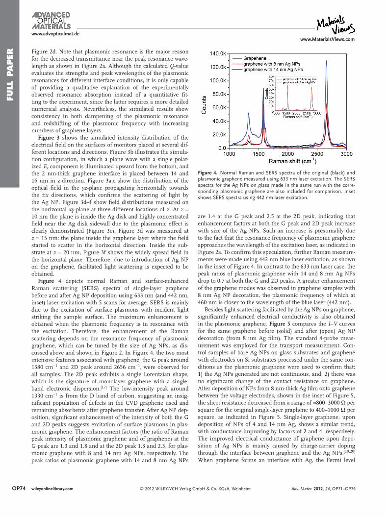
Figure 4. Normal Raman and SERS spectra of the original (black) and plasmonic graphene measured using 633 nm laser excitation. The SERS spectra for the Ag NPs on glass made in the same run with the corre-sponding plasmonic graphene are also included for comparison. Inset shows SERS spectra using 442 nm laser excitation.
Figure 2d. Note that plasmonic resonance is the major reason for the decreased transmittance near the peak resonance wave-length as shown in Figure 2a. Although the calculated Q-value evaluates the strengths and peak wavelengths of the plasmonic resonances for different interface conditions, it is only capable of providing a qualitative explanation of the experimentally observed resonance absorption instead of a quantitative fit-ting to the experiment, since the latter requires a more detailed numerical analysis. Nevertheless, the simulated results show consistency in both dampening of the plasmonic resonance and redshifting of the plasmonic frequency with increasing numbers of graphene layers.
Figure 3 shows the simulated intensity distribution of the electrical field on the surfaces of monitors placed at several dif-ferent locations and directions. Figure 3b illustrates the simula-tion configuration, in which a plane wave with a single polar-ized Ex component is illuminated upward from the bottom, and the 2 nm-thick graphene interface is placed between 14 and 16 nm in z-direction. Figure 3a,c show the distribution of the optical field in the yz-plane propagating horizontally towards the ±x directions, which confirms the scattering of light by the Ag NP. Figure 3d–f show field distributions measured on the horizontal xy-plane at three different locations of z. At z = 10 nm the plane is inside the Ag disk and highly concentrated field near the Ag disk sidewall due to the plasmonic effect is clearly demonstrated (Figure 3e). Figure 3d was measured at z = 15 nm: the plane inside the graphene layer where the field started to scatter in the horizontal direction. Inside the sub-strate at z = 20 nm, Figure 3f shows the widely spread field in the horizontal plane. Therefore, due to introduction of Ag NP on the graphene, facilitated light scattering is expected to be obtained.
Figure 4 depicts normal Raman and surface-enhanced Raman scattering (SERS) spectra of single-layer graphene before and after Ag NP deposition using 633 nm (and 442 nm, inset) laser excitation with 5 scans for average. SERS is mainly due to the excitation of surface plasmons with incident light striking the sample surface. The maximum enhancement is obtained when the plasmonic frequency is in resonance with the excitation. Therefore, the enhancement of the Raman scattering depends on the resonance frequency of plasmonic graphene, which can be tuned by the size of Ag NPs, as dis-cussed above and shown in Figure 2. In Figure 4, the two most intensive features associated with graphene, the G peak around 1580 cm−1 and 2D peak around 2656 cm−1, were observed for all samples. The 2D peak exhibits a single Lorentzian shape, which is the signature of monolayer graphene with a single-band electronic dispersion.[17] The low-intensity peak around 1330 cm−1 is from the D band of carbon, suggesting an insig-nificant population of defects in the CVD graphene used and remaining absorbents after graphene transfer. After Ag NP dep-osition, significant enhancement of the intensity of both the G and 2D peaks suggests excitation of surface plasmons in plas-monic graphene. The enhancement factors (the ratio of Raman peak intensity of plasmonic graphene and of graphene) at the G peak are 1.3 and 1.8 and at the 2D peak 1.3 and 2.5, for plas-monic graphene with 8 and 14 nm Ag NPs, respectively. The peak ratios of plasmonic graphene with 14 and 8 nm Ag NPs
© 2012 WILEY-VCH Verlag wileyonlinelibrary.com
are 1.4 at the G peak and 2.5 at the 2D peak, indicating that enhancement factors at both the G peak and 2D peak increase with size of the Ag NPs. Such an increase is presumably due to the fact that the resonance frequency of plasmonic graphene approaches the wavelength of the excitation laser, as indicated in Figure 2a. To confirm this speculation, further Raman measure-ments were made using 442 nm blue laser excitation, as shown in the inset of Figure 4. In contrast to the 633 nm laser case, the peak ratios of plasmonic graphene with 14 and 8 nm Ag NPs drop to 0.7 at both the G and 2D peaks. A greater enhancement of the graphene modes was observed in graphene samples with 8 nm Ag NP decoration, the plasmonic frequency of which at 460 nm is closer to the wavelength of the blue laser (442 nm).
Besides light scattering facilitated by the Ag NPs on graphene, significantly enhanced electrical conductivity is also obtained in the plasmonic graphene. Figure 5 compares the I–V curves for the same graphene before (solid) and after (open) Ag NP decoration (from 8 nm Ag film). The standard 4-probe meas-urement was employed for the transport measurement. Con-trol samples of bare Ag NPs on glass substrates and graphene with electrodes on Si substrates processed under the same con-ditions as the plasmonic graphene were used to confirm that: 1) the Ag NPs generated are not continuous, and; 2) there was no significant change of the contact resistance on graphene. After deposition of NPs from 8 nm-thick Ag film onto graphene between the voltage electrodes, shown in the inset of Figure 5, the sheet resistance decreased from a range of ≈800–3000 Ω per square for the original single-layer graphene to 400–1000 Ω per square, as indicated in Figure 5. Single-layer graphene, upon deposition of NPs of 4 and 14 nm Ag, shows a similar trend, with conductance improving by factors of 2 and 4, respectively. The improved electrical conductance of graphene upon depo-sition of Ag NPs is mainly caused by charge-carrier doping through the interface between graphene and the Ag NPs.[19,20] When graphene forms an interface with Ag, the Fermi level
GmbH & Co. KGaA, Weinheim Adv. Mater. 2012, 24, OP71–OP76

www.MaterialsViews.comwww.advopticalmat.de
FULL P
APER
Figure 5. Improved conductivity of single-layer graphene decorated with NPs formed from 8 nm-thick Ag, as compared to the original CVD graphene. Inset shows the schematics of 4-probe measurements of graphene and plasmonic graphene.
of graphene is shifted to the conduction band, resulting in the graphene being n-doped.[20] Since charge doping is sensitive to the metal/graphene interface, the significantly enhanced elec-trical conductivity observed in the plasmonic graphene sam-ples in this work suggests that a clean Ag/graphene interface could be formed if a the graphene surface is thoroughly cleaned before Ag deposition. In fact, the Ar/H2 anneal (see Experi-mental Section) before Ag deposition is a critical step to remove the residues on the transferred graphene to facilitate the for-mation of this clean interface. The much-enhanced electrical conductivity, in combination with the enhanced SERS, sug-gests that Ag NPs form a clean interface with CVD graphene. Charge transfer from Ag NPs to graphene through this inter-face results in doped graphene, and thus improved conduct-ance. This, in combination with the surface-plasmonic effect, makes plasmonic graphene a promising alternative to ITO or fluorine-doped tin oxide (FTO) for optoelectronic applications such as thin-film solar cells.
3. Conclusion
In conclusion, plasmonic graphene was fabricated on CVD graphene using thermally assisted self-assembly of Ag NPs from Ag thin films coated on graphene. Strong surface plas-monic resonance was confirmed from both transmittance and Raman measurements. The surface plasmonic resonance fre-quency shifts from 446 to 495 nm when the lateral dimension of Ag NPs increases from about 50 to 150 nm, as Ag film thick-ness changes from 4 to 14 nm. The presence of the graphene causes these frequencies to be redshifted as compared to the case without graphene. Both the plasmonic frequency and amplitude of surface plasmonic resonance decrease with increasing numbers of layers of graphene, which is consistent with the simulation. In addition, the plasmonic graphene shows much-improved electrical conductance (by a factor of 2–4) as compared to the original graphene. These results suggest plas-monic graphene transparent TCs could be used to enhance
© 2012 WILEY-VCH Verlag GmAdv. Mater. 2012, 24, OP71–OP76
[1] J. K. Wassei, R. B. Kaner, Mater. Today 2010, 13, 52. [2] F. Bonaccorso, Z. Sun, T. Hasan, A. C. Ferrari, Nat. Photonics 2010,
4, 611. [3] R. Czerw, B. Foley, D. Tekleab, A. Rubio, P. M. Ajayan, D. L. Carroll,
Phys. Rev. B 2002, 66, 033408. [4] S. Stankovich, D. A. Dikin, G. H. B. Dommett, K. M. Kohlhaas,
E. J. Zimney, E. A. Stach, R. D. Piner, S. T. Nguyen, R. S. Ruoff, Nature 2006, 442, 282.
[5] S. Bae, H. Kim, Y. Lee, X. F. Xu, J. S. Park, Y. Zheng, J. Balakrishnan, T. Lei, H. R. Kim, Y. I. Song, Y. J. Kim, K. S. Kim, B. Ozyilmaz, J. H. Ahn, B. H. Hong, S. Iijima, Nat. Nanotechnol. 2010, 5, 574.
[6] H. A. Atwater, A. Polman, Nat. Mater. 2010, 9, 205. [7] F. J. Beck, S. Mokkapati, K. R. Catchpole, Prog. Photovoltaics 2010,
18, 500.
light scattering and absorption in thin-film solar cells and other optoelectronic devices such as thin-film solar cells.
4. Experimental Section
Graphene was grown on commercial copper foils with 25 μm thickness at ∼1000 °C in a CVD system using a similar pro-cedure to that described elsewhere.[15] In order to transfer the graphene films onto other substrates, polymethyl methacrylate (PMMA) was first spin-coated on the surface of the as-grown graphene on copper. The sample was then placed in iron chlo-ride solution (0.1 g mL−1) to remove the copper foil, followed by rinsing with deionized (DI) water, soaking in DI water, and then being transferred to a selected substrate. After transfer-ring, the sample was baked at 80 °C for 1 h in an oven to elimi-nate moisture before removing the PMMA with acetone. The graphene was further treated in flowing Ar/H2 at 400 °C for 1 h to remove the PMMA residues.[18] Ag films of 4, 8, and 14 nm in thickness were deposited onto the graphene samples using electron-beam evaporation, with the Ag thickness being moni-tored in situ using a quartz crystal microbalance. The samples were then annealed in Ar/H2 at 260 °C for 30 min for Ag NP self assembly. 260 °C is the lower limit of the temperature window to obtain isolated Ag NPs for this experiment; lower processing temperatures were chosen to avoid damage to the plasmonic graphene.
Acknowledgements The authors acknowledge support from NSF EPSCoR for this work. JW was also supported in part by ARO contract No. ARO-W911NF-09–1–0295 and NSF contract Nos. NSF-DMR-0803149, 1105986, and NSF EPSCoR-0903806, and matching support from the State of Kansas through Kansas Technology Enterprise Corporation. Use of Raman instrumentation at Argonne’s Center for Nanoscale Materials was supported by the US DOE, Office of Science, Office of Basic Energy Sciences. The work performed at the Argonne National Laboratory was carried out under contract DE-AC02-06CH11357 between UChicago Argonne, LLC, and the US DOE.
Received: September 24, 2011 Revised: November 21, 2011
bH & Co. KGaA, Weinheim OP75wileyonlinelibrary.com

OP76
www.MaterialsViews.comwww.advopticalmat.de
FULL
PAPER
[8] S. S. Kim, S. I. Na, J. Jo, D. Y. Kim, Y. C. Nah, Appl. Phys. Lett. 2008, 93, 073307.
[9] M. I. Stockman, Phys. Today 2011, 64, 39.[10] F. J. Beck, A. Polman, K. R. Catchpole, J. Appl. Phys. 2009, 105,
114310.[11] S. Pillai, K. R. Catchpole, T. Trupke, M. A. Green, J. Appl. Phys. 2007,
101, 093105.[12] T. J. Echtermeyer, L. Britnell, P. K. Jasnos, A. Lombardo,
R. V. Gorbachev, A. N. Grigorenko, A. K. Geim, A. C. Ferrari, K. S. Novoselov, Nat. Commun. 2011, 2, 458.
[13] X. F. Wang, Y. P. Chen, D. D. Nolte, Opt. Express 2008, 16, 22105.[14] G. Xu, M. Tazawa, P. Jin, S. Nakao, K. Yoshimura, Appl. Phys. Lett.
2003, 82, 3811.
© 2012 WILEY-VCH Verlag wileyonlinelibrary.com
[15] J. Liu, G. Xu, C. Rochford, R. Lu, J. Wu, C. M. Edwards, C. L. Berrie, Z. Chen, V. A. Maroni, Appl. Phys. Lett. 2011, 99, 023111.
[16] FullWAVE Simulation package Version 6.0, by R-soft Design Group, 2007.
[17] A. C. Ferrari, J. C. Meyer, V. Scardaci, C. Casiraghi, M. Lazzeri, F. Mauri, S. Piscanec, D. Jiang, K. S. Novoselov, S. Roth, A. K. Geim, Phys. Rev. Lett. 2006, 97, 187401.
[18] M. Ishigami, J. H. Chen, W. G. Cullen, M. S. Fuhrer, E. D. Williams, Nano Lett. 2007, 7, 1643.
[19] G. Giovannetti, P. A. Khomyakov, G. Brocks, V. M. Karpan, J. van den Brink, P. J. Kelly, Phys. Rev. Lett. 2008, 101, 026803.
[20] Y. Ren, S. Chen, W. Cai, Y. Zhu, C. Zhu, R. S. Ruoff, Appl. Phys. Lett. 2010, 97, 053107.
GmbH & Co. KGaA, Weinheim Adv. Mater. 2012, 24, OP71–OP76