Physical Attacks on Tamper Resistance: Progress and Lessonssps32/ARO_2011.pdf · 2 Physical Attacks...
37
Physical Attacks on Tamper Resistance: Progress and Lessons 2 nd ARO Special Workshop on HW Assurance, Washington DC, 11-12 April 2011 Physical Attacks on Tamper Resistance: Progress and Lessons Dr Sergei Skorobogatov http://www.cl.cam.ac.uk/~sps32 email: [email protected]
Transcript of Physical Attacks on Tamper Resistance: Progress and Lessonssps32/ARO_2011.pdf · 2 Physical Attacks...

Physical Attacks on Tamper Resistance: Progress and Lessons 2nd ARO Special Workshop on HW Assurance, Washington DC, 11-12 April 2011
Physical Attacks on Tamper Resistance: Progress and Lessons
Dr Sergei Skorobogatovhttp://www.cl.cam.ac.uk/~sps32 email: [email protected]

2
Physical Attacks on Tamper Resistance: Progress and Lessons 2nd ARO Special Workshop on HW Assurance, Washington DC, 11-12 April 2011
Why do we need tamper resistance?• Theft of service: unauthorised access and fraud
– attacks on service providers (satellite TV, electronic meters, access cards, payment and banking cards, IP protection dongles)
• Access to information: stealing secrets and data– information recovery and extraction – gaining trade secrets (IP piracy)– ID theft
• Cloning and overbuilding: stealing intellectual property– copying to make money without having to spend on development– low-cost mass production by subcontractors
• Denial of service: attack business– dishonest competition– electronic warfare

3
Physical Attacks on Tamper Resistance: Progress and Lessons 2nd ARO Special Workshop on HW Assurance, Washington DC, 11-12 April 2011
Who needs secure chips?• Car industry
– anti-theft protection, spare parts identification
• Accessory control– mobile phone batteries, printer toner cartridges, memory modules
• Service and access control– RFID tags, access and payment cards, banking cards
• Home entertainment and consumer electronics– consumables, accessories, game consoles, digital media
• Intellectual property protection– software copy protection– protection of algorithms– protection against cloning and reverse engineering

4
Physical Attacks on Tamper Resistance: Progress and Lessons 2nd ARO Special Workshop on HW Assurance, Washington DC, 11-12 April 2011
Attack categories• Side-channel attacks
– techniques that allows monitoring the analog characteristics of supply, interface connections and any electromagnetic radiation
• Software attacks– use the normal communication interface and exploit security
vulnerabilities in the protocols, crypto-algorithms or implementation• Fault generation attacks
– use abnormal environmental conditions to generate malfunctions in the system that provide additional access
• Microprobing attacks– use access to the chip surface directly, so we can observe,
manipulate, and interfere with the device• Reverse engineering
– understand the inner structure of the device and learn or emulate its functionality; requires technology that is available to semiconductor manufacturers and gives similar capabilities to the attacker

5
Physical Attacks on Tamper Resistance: Progress and Lessons 2nd ARO Special Workshop on HW Assurance, Washington DC, 11-12 April 2011
Tamper protection levels
ZERO
D.G.Abraham et al. (IBM), 1991
LOW
LOW
MODL MODL
MODL

6
Physical Attacks on Tamper Resistance: Progress and Lessons 2nd ARO Special Workshop on HW Assurance, Washington DC, 11-12 April 2011
Tamper protection levels
MOD MOD MOD
MODH MODH

7
Physical Attacks on Tamper Resistance: Progress and Lessons 2nd ARO Special Workshop on HW Assurance, Washington DC, 11-12 April 2011
Tamper protection levels
HIGH
8
Physical Attacks on Tamper Resistance: Progress and Lessons 2nd ARO Special Workshop on HW Assurance, Washington DC, 11-12 April 2011
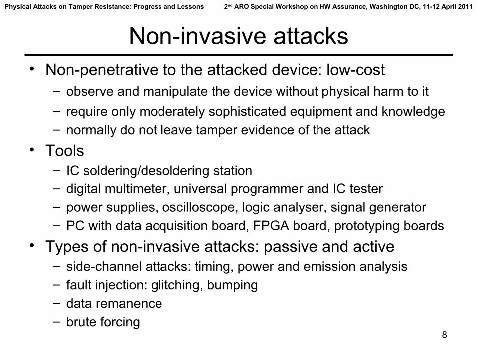
Non-invasive attacks• Non-penetrative to the attacked device: low-cost
– observe and manipulate the device without physical harm to it– require only moderately sophisticated equipment and knowledge– normally do not leave tamper evidence of the attack
• Tools– IC soldering/desoldering station– digital multimeter, universal programmer and IC tester– power supplies, oscilloscope, logic analyser, signal generator– PC with data acquisition board, FPGA board, prototyping boards
• Types of non-invasive attacks: passive and active– side-channel attacks: timing, power and emission analysis– fault injection: glitching, bumping– data remanence– brute forcing

9
Physical Attacks on Tamper Resistance: Progress and Lessons 2nd ARO Special Workshop on HW Assurance, Washington DC, 11-12 April 2011
Invasive attacks• Penetrative attacks: expensive to perform
– require expensive equipment, knowledgeable attackers and time– almost unlimited capabilities to extract information from chips
and understand their functionality– leave tamper evidence of the attack or even destroy the device
• Tools– IC soldering/desoldering station– simple chemical lab and high-resolution optical microscope– wire bonding machine, laser cutting system, microprobing station– oscilloscope, logic analyser, signal generator– scanning electron microscope and focused ion beam workstation
• Types of invasive attacks: passive and active– decapsulation, optical imaging, reverse engineering– microprobing and internal fault injection– chip modification

10
Physical Attacks on Tamper Resistance: Progress and Lessons 2nd ARO Special Workshop on HW Assurance, Washington DC, 11-12 April 2011
Semi-invasive attacks• Fill the gap between non-invasive and invasive attacks
– less damaging to target device (decapsulation without penetration)– less expensive and easier to setup and repeat than invasive attacks
• Tools– IC soldering/desoldering station– simple chemical lab and high-resolution optical microscope– UV light sources, lasers and special microscopes (laser scan, IR)– oscilloscope, logic analyser, signal generator– PC with data acquisition board, FPGA board, prototyping boards
• Types of semi-invasive attacks: passive and active– imaging: optical and laser techniques– fault injection: UV attack, photon injection, local heating, masking– side-channel attacks: optical emission analysis, induced leakage
11
Physical Attacks on Tamper Resistance: Progress and Lessons 2nd ARO Special Workshop on HW Assurance, Washington DC, 11-12 April 2011
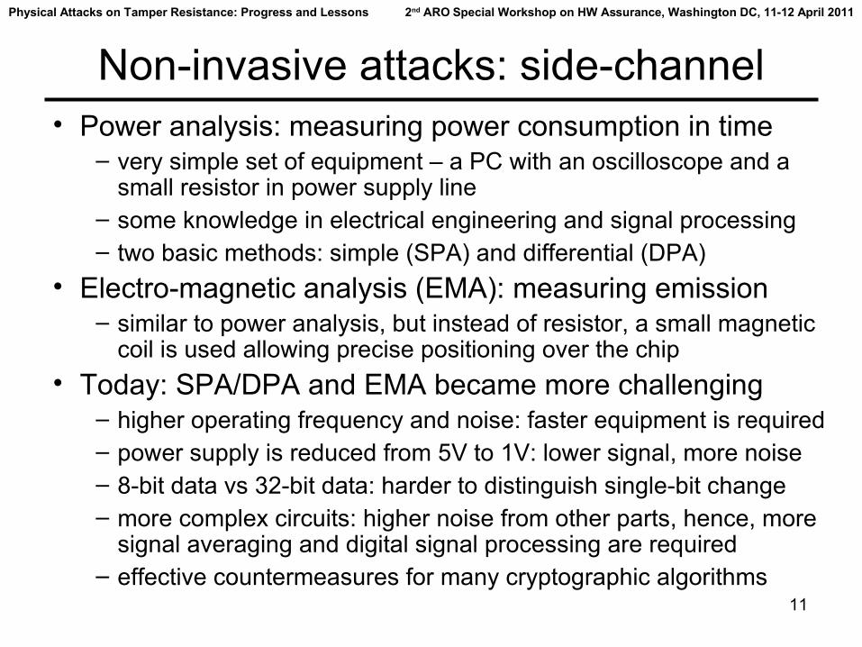
Non-invasive attacks: side-channel• Power analysis: measuring power consumption in time
– very simple set of equipment – a PC with an oscilloscope and a small resistor in power supply line
– some knowledge in electrical engineering and signal processing– two basic methods: simple (SPA) and differential (DPA)
• Electro-magnetic analysis (EMA): measuring emission– similar to power analysis, but instead of resistor, a small magnetic
coil is used allowing precise positioning over the chip• Today: SPA/DPA and EMA became more challenging
– higher operating frequency and noise: faster equipment is required– power supply is reduced from 5V to 1V: lower signal, more noise– 8-bit data vs 32-bit data: harder to distinguish single-bit change– more complex circuits: higher noise from other parts, hence, more
signal averaging and digital signal processing are required– effective countermeasures for many cryptographic algorithms

12
Physical Attacks on Tamper Resistance: Progress and Lessons 2nd ARO Special Workshop on HW Assurance, Washington DC, 11-12 April 2011
Non-invasive attacks: fault injection• Glitch attacks
– clock glitches– power supply glitches– corrupting data
• Security fuse verification in the Mask ROM bootloader of the Motorola MC68HC05B6 microcontroller
– double frequency clock glitch causes incorrect instruction fetch– low-voltage power glitch results in corrupted EEPROM data read
• Today: glitch attacks became harder to exploit– effective countermeasures are in place: clock and supply monitors– internal clock sources, clock conditioning and PLL circuits– internal charge pumps and voltage regulators– checksums (CRC, SHA-1) and encryption– asynchronous design

13
Physical Attacks on Tamper Resistance: Progress and Lessons 2nd ARO Special Workshop on HW Assurance, Washington DC, 11-12 April 2011
Invasive attacks: sample preparation• Decapsulation
– manual with fuming nitric acid (HNO3) and acetone at 60ºC– automatic using mixture of HNO3 and H2SO4
– partial or full– from front side and from rear side (just mechanical milling)
• Challenging process for small and BGA packages

14
Physical Attacks on Tamper Resistance: Progress and Lessons 2nd ARO Special Workshop on HW Assurance, Washington DC, 11-12 April 2011
Invasive attacks: reverse engineering• Reverse engineering – understanding the structure of a
semiconductor device and its functions– optical, using a confocal microscope (for >0.5μm chips)– deprocessing is necessary for chips with smaller technology– very challenging task for modern chips with millions of gates
Picture courtesy of Dr Markus Kuhn

15
Physical Attacks on Tamper Resistance: Progress and Lessons 2nd ARO Special Workshop on HW Assurance, Washington DC, 11-12 April 2011
• Memory extraction from Mask ROMs– removing top metal layers for direct optical observation of data in
NOR ROMs (bits programmed by presence of transistors)– for VTROM (ion implanted) used in many smartcards selective
(dash) etchants are required to expose the ROM bits
NEC μPD78F9116microcontroller0.35 μm
Motorola MC68HC05SC27smartcard1.0 μm
Picture courtesy of Dr Markus Kuhn
Invasive attacks: reverse engineering
16
Physical Attacks on Tamper Resistance: Progress and Lessons 2nd ARO Special Workshop on HW Assurance, Washington DC, 11-12 April 2011
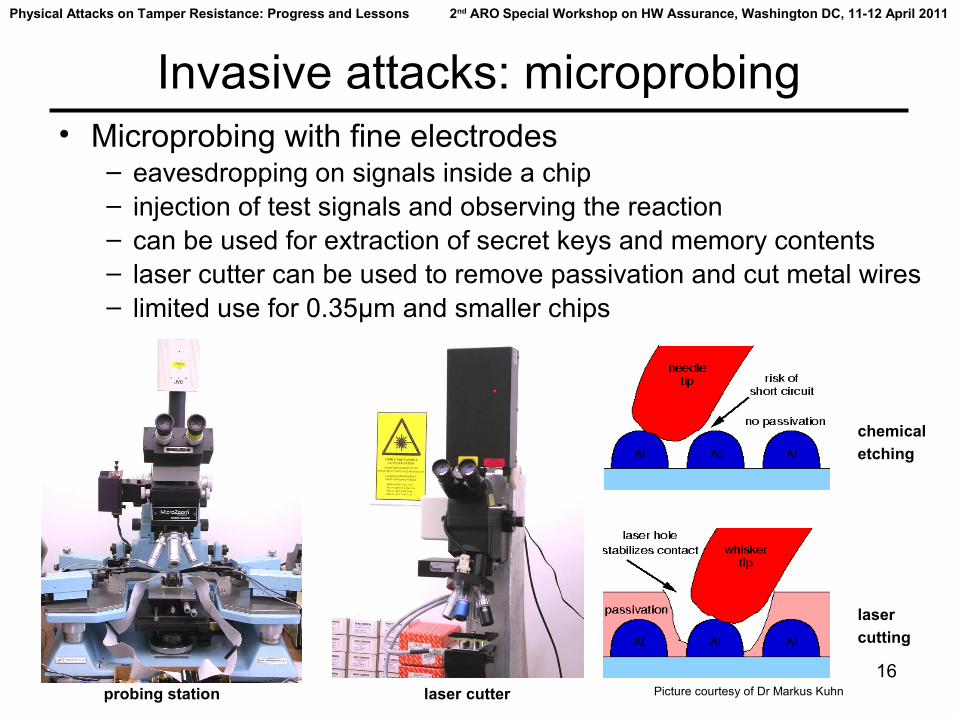
Invasive attacks: microprobing• Microprobing with fine electrodes
– eavesdropping on signals inside a chip– injection of test signals and observing the reaction– can be used for extraction of secret keys and memory contents– laser cutter can be used to remove passivation and cut metal wires– limited use for 0.35µm and smaller chips
Picture courtesy of Dr Markus Kuhnprobing station laser cutter
chemicaletching
lasercutting

17
Physical Attacks on Tamper Resistance: Progress and Lessons 2nd ARO Special Workshop on HW Assurance, Washington DC, 11-12 April 2011
Invasive attacks: chip modification• Focused Ion Beam (FIB) workstation
– chip-level surgery with 10 nm precision– etching with high aspect ratio– platinum and SiO2 deposition
Picture courtesy of Semiresearch Ltd
etchingpassivationand metal
depositplatinum

18
Physical Attacks on Tamper Resistance: Progress and Lessons 2nd ARO Special Workshop on HW Assurance, Washington DC, 11-12 April 2011
Semi-invasive attacks: imaging• Backside infrared imaging using IR-sensitive cameras
– Mask ROM extraction without chemical etching• Main option for 0.35µm and smaller chips
– multiple metal wires do not block the optical path
Texas Instruments MSP430F112microcontroller0.35 μm
Mask ROM inMotorola MC68HC705P6Amicrocontroller1.2 μm
19
Physical Attacks on Tamper Resistance: Progress and Lessons 2nd ARO Special Workshop on HW Assurance, Washington DC, 11-12 April 2011
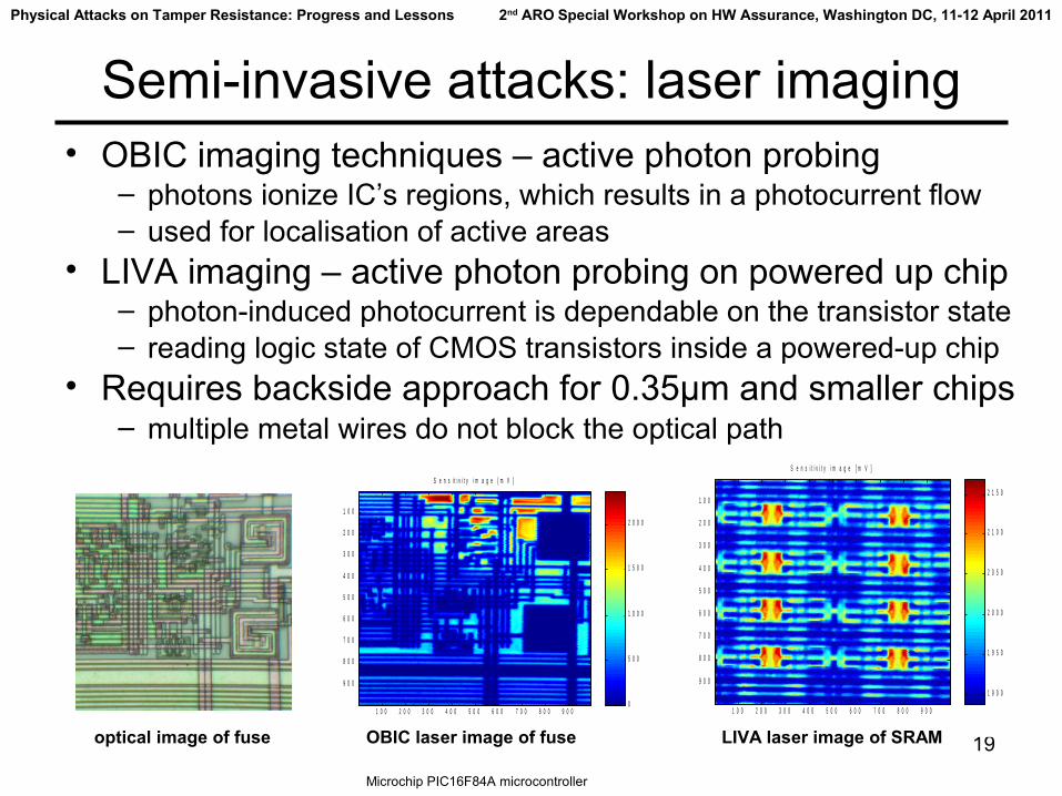
Semi-invasive attacks: laser imaging• OBIC imaging techniques – active photon probing
– photons ionize IC’s regions, which results in a photocurrent flow– used for localisation of active areas
• LIVA imaging – active photon probing on powered up chip– photon-induced photocurrent is dependable on the transistor state– reading logic state of CMOS transistors inside a powered-up chip
• Requires backside approach for 0.35µm and smaller chips– multiple metal wires do not block the optical path
S e n s i t i v i t y i m a g e [ m V ]
1 0 0 2 0 0 3 0 0 4 0 0 5 0 0 6 0 0 7 0 0 8 0 0 9 0 0
1 0 0
2 0 0
3 0 0
4 0 0
5 0 0
6 0 0
7 0 0
8 0 0
9 0 0
0
5 0 0
1 0 0 0
1 5 0 0
2 0 0 0
Microchip PIC16F84A microcontroller
S e n s i t i v i t y i m a g e [ m V ]
1 0 0 2 0 0 3 0 0 4 0 0 5 0 0 6 0 0 7 0 0 8 0 0 9 0 0
1 0 0
2 0 0
3 0 0
4 0 0
5 0 0
6 0 0
7 0 0
8 0 0
9 0 01 9 0 0
1 9 5 0
2 0 0 0
2 0 5 0
2 1 0 0
2 1 5 0
optical image of fuse OBIC laser image of fuse LIVA laser image of SRAM

20
Physical Attacks on Tamper Resistance: Progress and Lessons 2nd ARO Special Workshop on HW Assurance, Washington DC, 11-12 April 2011
Semi-invasive attacks: fault injection• Optical fault injection attack
– using laser attached to microscope to inject fault into chip operation– chip is decapsulated and placed on a test board under microscope– red laser (635nm) for front approach and IR (1065nm) for backside– control board is used to operate the chip and trigger the laser pulse
• Tested on chips down to 90nm and proved its effectiveness– requires backside approach for modern chips due to metal layers– cannot be scaled down to individual transistor, but still effective
test board test setup control board

21
Physical Attacks on Tamper Resistance: Progress and Lessons 2nd ARO Special Workshop on HW Assurance, Washington DC, 11-12 April 2011
Semi-invasive attacks: fault injection• Actel secure FPGA (A3P250, 130nm) with JTAG interface
– possibility of attack proposed in 2002 and demonstrated in 2010• Locating Flash and active areas is easy via laser scanning• Sensitive locations were found with exhaustive search
20µm grid: black – data corrupted, white – matching predicted data
backside laser scanning image fault injection sensitive locations
22
Physical Attacks on Tamper Resistance: Progress and Lessons 2nd ARO Special Workshop on HW Assurance, Washington DC, 11-12 April 2011
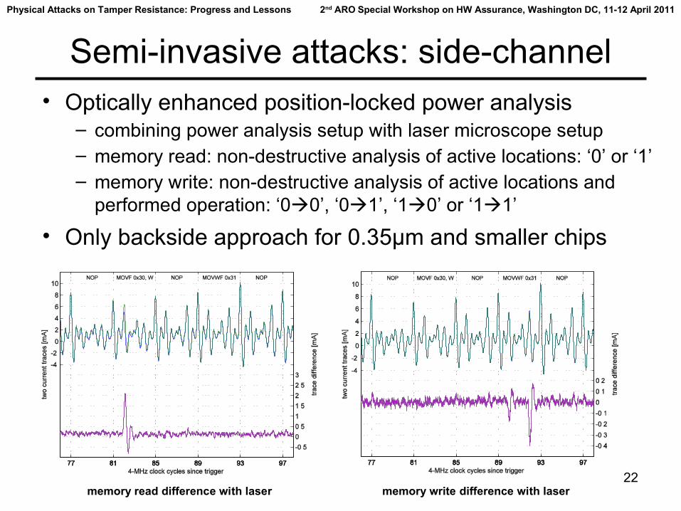
Semi-invasive attacks: side-channel• Optically enhanced position-locked power analysis
– combining power analysis setup with laser microscope setup– memory read: non-destructive analysis of active locations: ‘0’ or ‘1’– memory write: non-destructive analysis of active locations and
performed operation: ‘00’, ‘01’, ‘10’ or ‘11’
• Only backside approach for 0.35µm and smaller chips
memory read difference with laser memory write difference with laser

23
Physical Attacks on Tamper Resistance: Progress and Lessons 2nd ARO Special Workshop on HW Assurance, Washington DC, 11-12 April 2011
Semi-invasive attacks: side-channel• Optical emission analysis
– transistors emit photons when they switch– 10−2 to 10−4 photons per switch with peak in IR region (900-1200nm)– comes from area close to drain and mainly from NMOS transistor– optical emission can be detected with PMT and CCD cameras
PMT setup
CCD setup
crosssection

24
Physical Attacks on Tamper Resistance: Progress and Lessons 2nd ARO Special Workshop on HW Assurance, Washington DC, 11-12 April 2011
Semi-invasive attacks: side-channel• Optical emission analysis
– Microchip PIC16F628 microcontroller with test code at 20 Mhz; PMT vs SPA and CCD camera images in just 10 minutes
• Only backside approach for 0.35µm and smaller chips– successfully tested on chips down to 130nm (higher Vcc, >1 hour)
PMT
SPA
optical
IR CCD

25
Physical Attacks on Tamper Resistance: Progress and Lessons 2nd ARO Special Workshop on HW Assurance, Washington DC, 11-12 April 2011
Comparing the attack methods• Target: Actel ProASIC3 secure FPGA family (military use)
– secure configuration data update using AES-128 encryption– designed to prevent IP theft, cloning and overbuilding
• Can we attack the AES key used for bitstream encryption?– if the AES key is known then the device can be cloned
• Invasive attacks (expensive)– partial reverse engineering followed by microprobing
• Semi-invasive attacks (affordable)– optical fault injection attack– optical emission analysis
• Non-invasive attacks (simple)– side-channel attacks such as SPA, DPA, CPA, EMA, DEMA– poor signal-to-noise ratio of about −15dB due to low-power
operation and multiple sources of noise (internal clock operaton, charge pumps, low level of the leakage signal)
26
Physical Attacks on Tamper Resistance: Progress and Lessons 2nd ARO Special Workshop on HW Assurance, Washington DC, 11-12 April 2011
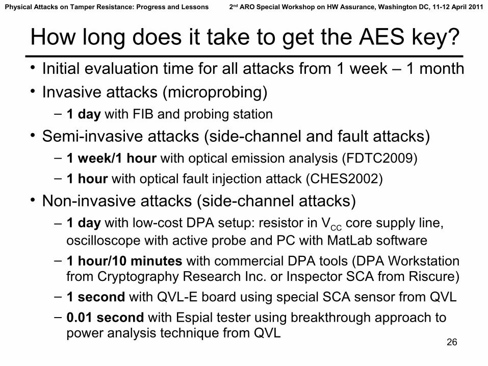
How long does it take to get the AES key?• Initial evaluation time for all attacks from 1 week – 1 month• Invasive attacks (microprobing)
– 1 day with FIB and probing station• Semi-invasive attacks (side-channel and fault attacks)
– 1 week/1 hour with optical emission analysis (FDTC2009)– 1 hour with optical fault injection attack (CHES2002)
• Non-invasive attacks (side-channel attacks)– 1 day with low-cost DPA setup: resistor in VCC core supply line,
oscilloscope with active probe and PC with MatLab software– 1 hour/10 minutes with commercial DPA tools (DPA Workstation
from Cryptography Research Inc. or Inspector SCA from Riscure)– 1 second with QVL-E board using special SCA sensor from QVL– 0.01 second with Espial tester using breakthrough approach to
power analysis technique from QVL

27
Physical Attacks on Tamper Resistance: Progress and Lessons 2nd ARO Special Workshop on HW Assurance, Washington DC, 11-12 April 2011
New technology to improve attacks• Standard side-channel
analysis setup
• New more efficient setup
• Plus another 9 problems to address and solve in order to get an average of 1'000'000 times improvement
– in reality from 1'000 to 1'000'000'000'000 times improvement

28
Physical Attacks on Tamper Resistance: Progress and Lessons 2nd ARO Special Workshop on HW Assurance, Washington DC, 11-12 April 2011
QVL technology• Overview
– new approach to sensor technology: precision measurements with higher sensitivity and lower noise compared to standard technology
– does not add new attacks – just revisit the existing: what was not possible due to high cost and long time required, becomes feasible
• Capabilities– extract cryptographic keys and passwords– reverse engineering of algorithms and internal operations– monitor device activity to spot faults, trojans and backdoors
• Applications– failure analysis, security evaluation, chip health monitoring– scanning for trojans and backdoors inserted by third parties
• Information– QVL technology is being evaluated for various secure chips– http://www.quovadislabs.com/

29
Physical Attacks on Tamper Resistance: Progress and Lessons 2nd ARO Special Workshop on HW Assurance, Washington DC, 11-12 April 2011
Quest for trojans and backdoors• What x1'000'000 improvement would mean for real device?
– 1 day for an attack which normally takes 2000 years to succeed– 1 second for an attack which normally takes 10 days to succeed
• It might be OK to have backdoors and trojans in highly secure devices, but they should be kept secret and never used to boost the existing security measures
• QVL technology was successfully tested on real chips– Actel secure FPGAs: ProASIC3, Igloo, Fusion and SmartFusion
• Actel secure FPGAs have some security engineering bugs– it is possible to use the secret factory access key for generating
authentication signature with AES and then attack it with SCA– latest generation of Flash FPGA devices share the same key
• What can be done if the backdoor secret key is known?– turn some ROM areas (OTP) into reprogrammable Flash areas– reprogram low-level features– access hidden JTAG registers– access secret data, information, configuration and IP

30
Physical Attacks on Tamper Resistance: Progress and Lessons 2nd ARO Special Workshop on HW Assurance, Washington DC, 11-12 April 2011
Defence technologies: tamper protection• Help comes from chip fabrication technology
– planarisation as a part of modern chip fabrication process (0.5 μm or smaller feature size)
– moving away from building blocks which are easily identifiable and have easily traceable data paths
– glue logic design makes reverse engineering much harder– multiple metal layers block any direct access– small size of transistors makes attacks less feasible– chips operate at higher frequency and consume less power– smaller and BGA packages scare off many attackers
0.9µm 0.5µm MC68HC908AZ60Amicrocontroller
Scenix SX28microcontroller

31
Physical Attacks on Tamper Resistance: Progress and Lessons 2nd ARO Special Workshop on HW Assurance, Washington DC, 11-12 April 2011
Defence technologies: tamper protection• Additional protections
– top metal layers with sensors– voltage, frequency and temperature sensors– memory access protection, crypto-coprocessors– internal clocks, power supply pumps– asynchronous logic design, symmetric design, dual-rail logic– ASICs, secure FPGAs and custom-designed ICs– software countermeasures
STMicroelectronics ST16 smartcard Fujitsu custom secure chip

32
Physical Attacks on Tamper Resistance: Progress and Lessons 2nd ARO Special Workshop on HW Assurance, Washington DC, 11-12 April 2011
• Security advertising without proof– no means of comparing security, lack of independent analysis– no guarantee and no responsibility from chip manufacturers– wide use of magic words: protection, encryption, authentication,
unique, highly secure, strong defence, cannot be, unbreakable, impossible, uncompromising, buried under x metal layers
• Constant economics pressure on cost reduction– less investment, hence, cheaper solutions and outsourcing– security via obscurity approach
• Quicker turnaround– less testing, hence, more bugs
• What about backdoors?– access to the on-chip data for factory testing purposes– how reliably was this feature disabled?– how difficult is to attack the access port?– are there any trojans deliberately inserted by subcontractors?
Defence technologies: what goes wrong
33
Physical Attacks on Tamper Resistance: Progress and Lessons 2nd ARO Special Workshop on HW Assurance, Washington DC, 11-12 April 2011
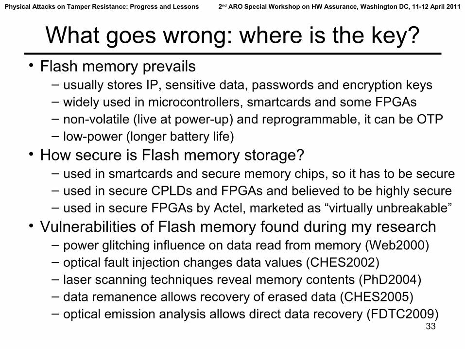
What goes wrong: where is the key?• Flash memory prevails
– usually stores IP, sensitive data, passwords and encryption keys– widely used in microcontrollers, smartcards and some FPGAs– non-volatile (live at power-up) and reprogrammable, it can be OTP– low-power (longer battery life)
• How secure is Flash memory storage?– used in smartcards and secure memory chips, so it has to be secure– used in secure CPLDs and FPGAs and believed to be highly secure– used in secure FPGAs by Actel, marketed as “virtually unbreakable”
• Vulnerabilities of Flash memory found during my research– power glitching influence on data read from memory (Web2000)– optical fault injection changes data values (CHES2002)– laser scanning techniques reveal memory contents (PhD2004)– data remanence allows recovery of erased data (CHES2005)– optical emission analysis allows direct data recovery (FDTC2009)

34
Physical Attacks on Tamper Resistance: Progress and Lessons 2nd ARO Special Workshop on HW Assurance, Washington DC, 11-12 April 2011
Defence technologies: how it fails• Microchip PIC microcontroller: software attack on security
– security fuse can be reset without erasing the code/data memory• Atmel AVR microcontroller: glitch attack on security fuse
– security fuse can be reset without erasing the code/data memory• Hitachi smartcard: information leakage on a products CD
– full datasheet on the smartcard was placed by mistake on user CD• Xilinx secure CPLD: programming software bug
– security fuse incorrectly programmed resulting in no protection• Dallas SHA-1 secure memory: factory initialisation bug
– security features were not activated resulting in easy access to key• Actel secure FPGA: programming software bug
– Flash FPGA devices were always programmed with 00..00 passkey• Other possible ways of security failures
– insiders, datasheets of similar products, development tools, patents

35
Physical Attacks on Tamper Resistance: Progress and Lessons 2nd ARO Special Workshop on HW Assurance, Washington DC, 11-12 April 2011
Conclusion• There is no such a thing as absolute protection
– given enough time and resources any protection can be broken• Attack technologies are constantly evolving
– do not underestimate capabilities of the attackers– technical progress reduces cost of already known attacks
• Defence should be ahead of attack technologies– security hardware engineers must be familiar with existing attack
technologies to develop adequate protection– many chips unavoidably have backdoors as a part of fabrication
and testing process, but they must be made as secure as possible to prevent easy target
• Many vulnerabilities were found in various secure chips and more are to be found posing more challenges to hardware security engineers

36
Physical Attacks on Tamper Resistance: Progress and Lessons 2nd ARO Special Workshop on HW Assurance, Washington DC, 11-12 April 2011
Future work• Data remanence analysis of Flash in modern chips to
estimate possibility to recover previously erased data• Improving side-channel attacks with new techniques• Testing various chips against QVL technology: if it is
possible to reduce the attack time from hours to seconds in some secure devices, is it possible to reduce the attack time on highly secure devices from years to days?
37
Physical Attacks on Tamper Resistance: Progress and Lessons 2nd ARO Special Workshop on HW Assurance, Washington DC, 11-12 April 2011
References• Questions are welcomed via email:
– [email protected]• Slides
– http://www.cl.cam.ac.uk/~sps32/ARO_2011.pdf• Literature
– http://www.cl.cam.ac.uk/~sps32/– http://www.cl.cam.ac.uk/~sps32/#Publications