PHOTOVOLTAIC DETECTORS: p-n JUNCTIONdial/ece425/pvdetnotes.pdf · PV LECTURE 1 PHOTOVOLTAIC...
27
PV LECTURE 1 PHOTOVOLTAIC DETECTORS: p-n JUNCTION Two opposite impurity-doped semiconductors: n-type (donor, As, Sb, P) electrons are majority carriers holes are minority carriers p-type (acceptor, Al, B, In, Ga) holes are majority carriers electrons are minority carriers Majority carriers mobile, minority carriers not. JUNCTION FORMATION: 1. Free electrons in n-region attracted to positive charge in p-region, drift on over 2. Free holes in p-region attracted to negative charge in n-region, drift on over 3. Leaves n-region with net positive charge and p-region with net negative charge. Whole crystal neutral 4. Potential barrier formed at junction.
Transcript of PHOTOVOLTAIC DETECTORS: p-n JUNCTIONdial/ece425/pvdetnotes.pdf · PV LECTURE 1 PHOTOVOLTAIC...

PV LECTURE 1
PHOTOVOLTAIC DETECTORS: p-n JUNCTION
Two opposite impurity-doped semiconductors:
n-type (donor, As, Sb, P)
electrons are majority carriers
holes are minority carriers
p-type (acceptor, Al, B, In, Ga)
holes are majority carriers
electrons are minority carriers
Majority carriers mobile, minority carriers not.
JUNCTION FORMATION:
1. Free electrons in n-region attracted to positive
charge in p-region, drift on over
2. Free holes in p-region attracted to negative
charge in n-region, drift on over
3. Leaves n-region with net positive charge and
p-region with net negative charge. Whole
crystal neutral
4. Potential barrier formed at junction.

PV LECTURE 2
VALENCE BAND
DONOR LEVELE f
CONDUCTION BAND
ACCEPTOR LEVEL
P-TYPE
E g
φφ
N-TYPE
DEPLETIONREGION
Height of potential barrier φφ depends upon donor
and acceptor energy levels and concentrations.
φ ≈kT
q
n p
nn p
i
ln2
nn = electrons in n-region (majority carriers)
pp = holes in p-region (majority carriers)
ni2 = intrinsic carrier concentration
Since ni is strong function of temperature,
as T↑↑, φφ↓↓
Fermi level constant in equilibrium junction

PV LECTURE 3
BIASING THE p-n JUNCTION
Apply external bias across junction
FORWARD BIAS: barrier height reduced; high current,
due to majority carriers; depletion region
narrower
VALENCE BAND
DONOR LEVELE f
N-TYPE
DEPLETIONREGION
CONDUCTION BAND
ACCEPTOR LEVEL
P-TYPE
Eg
φφ -Vf
Vf
+
Vf
REVERSE BIAS: barrier height increased; low current
due to minority carriers; depletion region wider

PV LECTURE 4
CONDUCTION BAND
ACCEPTOR LEVEL
VALENCE BAND
DONOR LEVELE f
N-TYPE
DEPLETIONREGION
φφ
P-TYPE
Eg
+Vr
Vr
+
Vr

PV LECTURE 5
I-V CHARACTERISTICSI-V CHARACTERISTICS
Equation of I-V characteristics of p-n junction diode:
I I eo
qV
kT= −FHG
IKJ
β 1
where Io = reverse saturation current,
q = electronic charge = 1.602 177 33 (49) ××10-19 C
V = applied voltage
ββ = “fudge factor,” to make the equation fit the
data; varies between 1 and 3, voltage
dependent.
k = Boltzmann’s constant = 1.380658 (12) ××10-23 J/K
T = temperature (K) (q/kT≈≈38.7 @ 300K)
-5.00E-08
0.00E+00
5.00E-08
1.00E-07
-0.5 -0.4 -0.3 -0.2 -0.1 0 0.1 0.2
VOLTAGE
CURRENT vs. VOLTAGE for VARIOUS Io
PV LECTURE 6
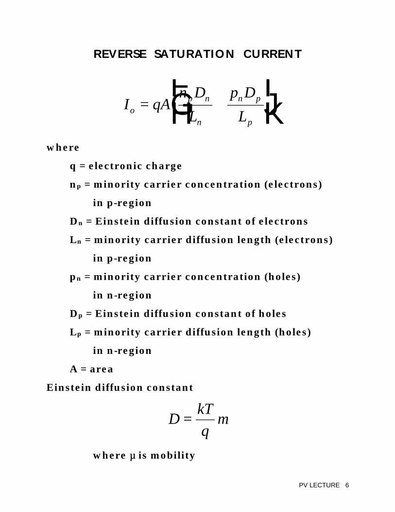
REVERSE SATURATION CURRENT
I qAn D
L
p D
Lop n
n
n p
p
= +FHG
IKJ
where
q = electronic charge
np = minority carrier concentration (electrons)
in p-region
Dn = Einstein diffusion constant of electrons
Ln = minority carrier diffusion length (electrons)
in p-region
pn = minority carrier concentration (holes)
in n-region
Dp = Einstein diffusion constant of holes
Lp = minority carrier diffusion length (holes)
in n-region
A = area
Einstein diffusion constant
DkT
q= µ
where µµ is mobility
PV LECTURE 7
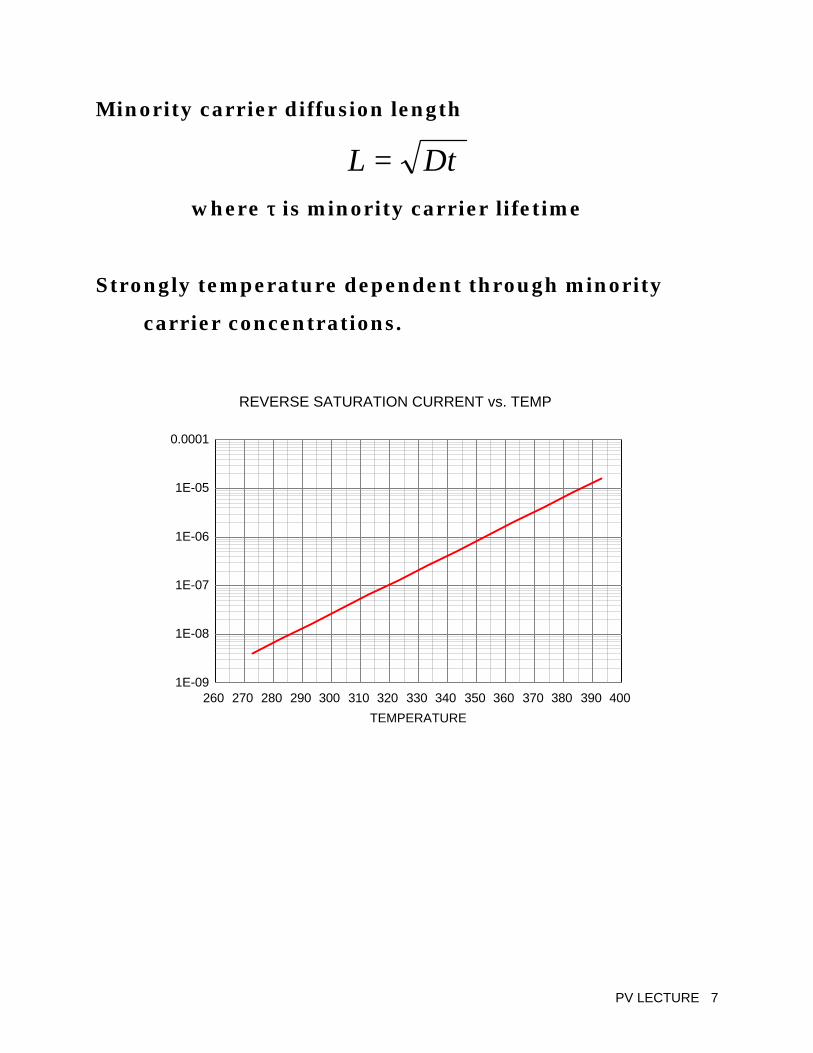
Minority carrier diffusion length
L D= τwhere ττ is minority carrier lifetime
Strongly temperature dependent through minority
carrier concentrations.
1E-09
1E-08
1E-07
1E-06
1E-05
0.0001
260 270 280 290 300 310 320 330 340 350 360 370 380 390 400
TEMPERATURE
REVERSE SATURATION CURRENT vs. TEMP

PV LECTURE 8
p-n JUNCTION PHOTODIODE
METAL CONTACT
N-TYPE BULK SILICON
A-R COAT
ACTIVE AREA
SiO2
P+ DIFFUSION
DEPLETION REGION
Photon with energy >Eg creates electron-hole pair.
λ λ µcgE
in m=12398. b g
Carriers generated within depletion region are
immediately separated by potential across barrier.
Carriers generated outside depletion region may
diffuse to junction to be separated by potential
barrier. Governed by minority carrier diffusion
length and carrier lifetime.
Result: voltage generated across barrier; magnitude
related to potential barrier height φφ and amount of
light.
PV LECTURE 9
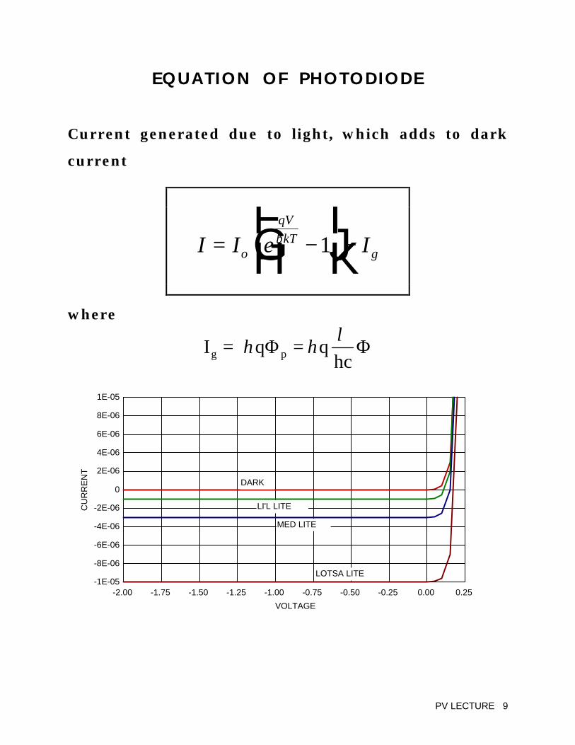
EQUATION OF PHOTODIODE
Current generated due to light, which adds to dark
current
I I e Io
qV
kTg= −
FHG
IKJ −β 1
where
I = q qhcg pη ηλ
Φ Φ=
-1E-05
-8E-06
-6E-06
-4E-06
-2E-06
0
2E-06
4E-06
6E-06
8E-06
1E-05
CU
RR
EN
T
-2.00 -1.75 -1.50 -1.25 -1.00 -0.75 -0.50 -0.25 0.00 0.25
VOLTAGE
DARK
LI'L LITE
MED LITE
LOTSA LITE

PV LECTURE 10
QUANTUM EFFICIENCY
Photons with λλ > λλc not absorbed
Electron-hole pairs created outside depletion regionnot all utilized
Electron-hole pairs created beyond diffusion length notutilized (increase depletion width via reverse bias)
Surface recombination (passivate)
Optical losses [reflection (A-R coat) and transmission]
Most photons have more energy than needed to createelectron-hole pair - excess energy just heats
Barrier height less than Eg

PV LECTURE 11
OPERATING POINTS
SHORT-CIRCUIT CURRENT: At V = 0, I = -Ig which is
linear with incident radiant power.
OPEN-CIRCUIT VOLTAGE: At I = 0, then
V = kT
qln
I + I
Ioco g
o
β LNM
OQP
If Ig >> Io, Voc is logarithmic with radiant power.
0
0.05
0.1
0.15
Voc
0.01 0.1 1 10 100
RATIO (Ig/Io)
for Ig >> Io, it's logarithmic
PERFECTLOGARITHMIC
PV LECTURE 12
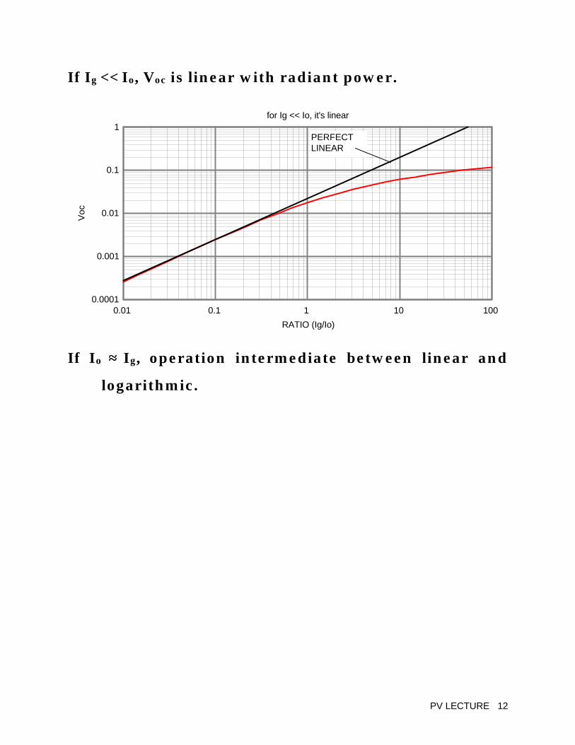
If Ig << Io, Voc is linear with radiant power.
0.0001
0.001
0.01
0.1
1
Voc
0.01 0.1 1 10 100
RATIO (Ig/Io)
for Ig << Io, it's linear
PERFECTLINEAR
If Io ≈≈ Ig, operation intermediate between linear and
logarithmic.
PV LECTURE 13
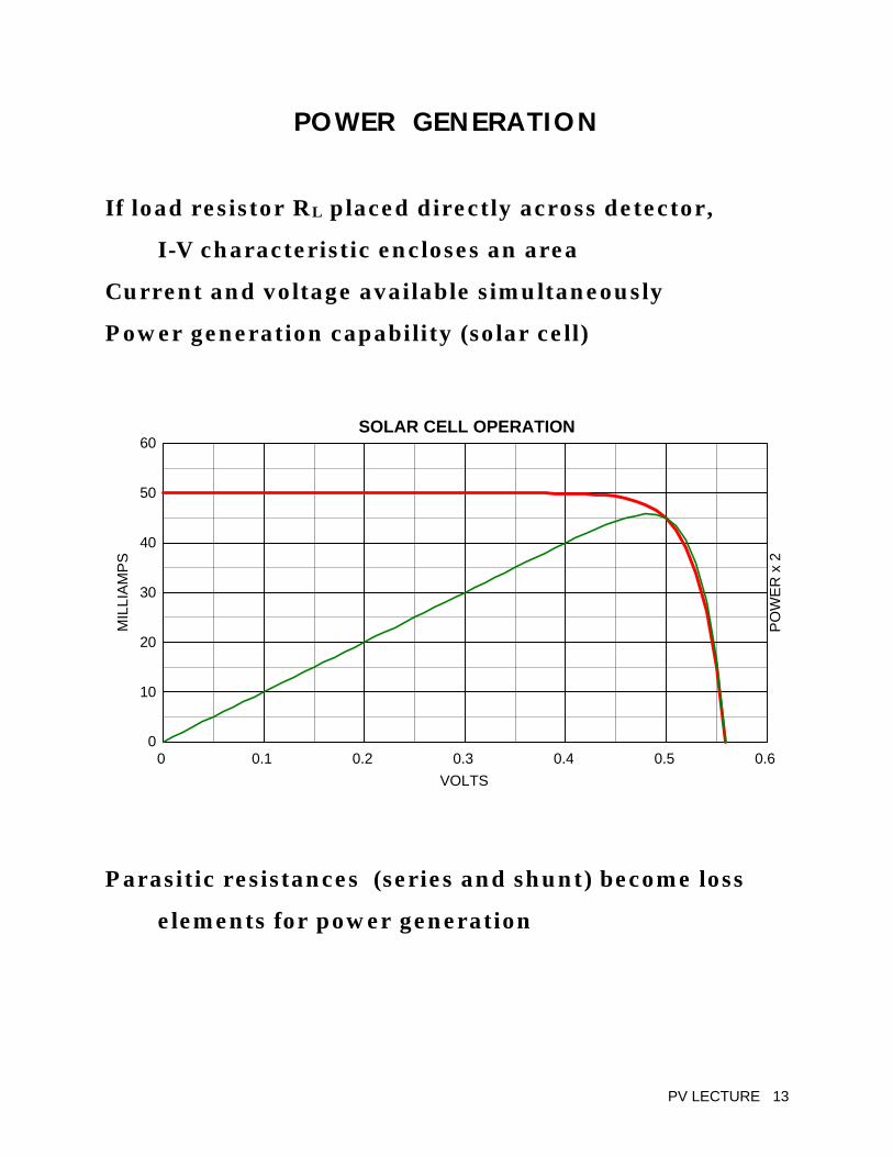
POWER GENERATION
If load resistor RL placed directly across detector,
I-V characteristic encloses an area
Current and voltage available simultaneously
Power generation capability (solar cell)
0
10
20
30
40
50
60
MIL
LIA
MP
S
PO
WE
R x
20 0.1 0.2 0.3 0.4 0.5 0.6
VOLTS
SOLAR CELL OPERATION
Parasitic resistances (series and shunt) become loss
elements for power generation

PV LECTURE 14
REVERSE BIASING THE PHOTODIODE
Bias into third quadrant; requires voltage source and
load resistor
-2E-06
-1.5E-06
-1E-06
-5E-07
0
5E-07
1E-06
1.5E-06
2E-06
CU
RR
EN
T
-10.00 -9.00 -8.00 -7.00 -6.00 -5.00 -4.00 -3.00 -2.00 -1.00 0.00 1.00
VOLTAGE
DARK
LITE
Vb
LOAD LINE
I = -Io -Ig
ADVANTAGES:
1. Better long-wavelength response due to less
recombination
2. Increased speed due to electric field which
sweeps carriers out
3. Increased speed due to lower junction
capacitance C = const (V-0.6)n, -1/2<x<-1/3
DISADVANTAGES:
1. Presence of Io and its temperature dependence
2. Requires relatively stable, quiet voltage source

PV LECTURE 15
PHOTOVOLTAIC DETECTOR CHARACTERISTICS
Responsivity
ℜ = ηλ
qhc
0
0.2
0.4
0.6
0.8
1
RE
SP
ON
SIV
ITY
(A
/W)
0 0.2 0.4 0.6 0.8 1
WAVELENGTH (um)
Noises
Shot due to current (signal, background, dark)
i q i i i BS sig bkgnd dark= + +2 ( )
Johnson (dynamic resistance)
ikTB
RJdyn
=4
1/f (contacts)
iconst I df
ff
dc1 =
⋅z

PV LECTURE 16
LIMITING NOISE IN PHOTOVOLTAICS
Signal equation
i qhc
qs p= = =Φℜ Φ Φηλ
η
Shot noise due to current flow limits
i qi Bn DC2 2=
iDC from signal (visible) and background (infrared)
i qhc
B q Bn p2 2 22 2= =η
ληΦ Φ
Di
i
AB
hcE hc EBLIPs
n p
* = ⋅ = =Φ
ηλ λ η2 2
Better than photoconductive detector by 2 .
No recombination noise

PV LECTURE 17
PHOTOVOLTAIC DETECTOR CHARACTERISTICSII
Linearity
At short-circuit current for high-quality photo-diodes, easy to demonstrate linear over sevendecades, claimed linear to 14 decades
Dynamic resistance
RdV
dI
kT
qIed
o
qV AkT= = −β
At zero bias it becomes
RdV
dI
kT
qIdo
= =β
As T↑↑, Rd↓↓
• • For minimum Johnson noise current due to detector
resistance, need high R.
• • Longer λλ photodiodes have lower Eg, higher Io, lower
Rd, and are noisier.

PV LECTURE 18
DETERMINATION OF ββ AND Io
Determine short-circuit current (Isc) and open-circuit
voltage (Voc) as a function of light level
Plot log(Isc) vs. Voc
Slope of best-fit straight line is ββ
Current at intercept (V=0) is Io
1E-09
1E-08
1E-07
1E-06
1E-05
1E-04
1E-03
1E-02
1E-01
1E+00
0 0.1 0.2 0.3 0.4 0.5 OPEN-CIRCUIT VOLTAGE
DETERMINATION OF beta AND Io
SLOPE IS beta
INTERCEPT IS Io

PV LECTURE 19
PHOTOVOLTAIC DETECTOR MATERIALS
MATERIAL Eg (eV) λλc (µµm) NOTES
GaP 2.4 0.52
GaAs 1.4 0.93
Si 1.12 1.1 indirect
InGaAs 0.73 1.7
Ge 0.68 1.82 indirect
InGaAs 0.59 2.1
InGaAs 0.50 2.5
InAs 0.28 3.5
InSb 0.16 5.5
HgCdTe variable variable variable
PbSnTe variable variable variable

PV LECTURE 20
P-I-N PHOTODIODES
Fabricated with wide depletion layer, occupies most ofstructure
METAL CONTACT
A-R COAT
ACTIVE AREA
SiO2
P+ DIFFUSION
INTRINSIC REGION
N+ REGION
Needs reverse bias for electric field to sweep out
carriers
Low capacitance (<5pF)
Fast! (to 60 GHz)
Available in small (25 µµm) to medium (1 mm) sizes
Materials: Si, InGaAs/InP (point, fiber pigtail)

PV LECTURE 21
AVALANCHE PHOTODIODE
Operate at high reverse bias below breakdown; carriers
moving through intrinsic region can free others
Gain up to 1000 is available, voltage dependent.
Bias (100-300V) and gain temperature sensitive, use
regulated current bias for best stability
Noise greater than pin photodiode, goes as Gx, x<1<2

PV LECTURE 22
AVALANCHE PHOTODIODE II
Can count individual photons if cooled (77K) and
biased beyond breakdown (Geiger mode)
Silicon, germanium and some mixed heterojunction
photodiodes (InGaAs)
Speed: to 1 Ghz (slower than pin, gain mechanism
takes time)
Application: Fast detectors with gain, for digital fiber
optic communications systems when limiting noise
comes from support electronics.
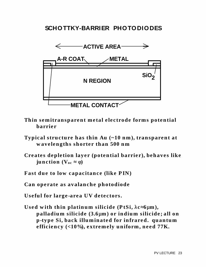
PV LECTURE 23
SCHOTTKY-BARRIER PHOTODIODES
METAL CONTACT
A-R COAT
ACTIVE AREA
SiO2N REGION
METAL
Thin semitransparent metal electrode forms potentialbarrier
Typical structure has thin Au (~10 nm), transparent atwavelengths shorter than 500 nm
Creates depletion layer (potential barrier), behaves likejunction (Voc ≈≈ φφ)
Fast due to low capacitance (like PIN)
Can operate as avalanche photodiode
Useful for large-area UV detectors.
Used with thin platinum silicide (PtSi, λλc≈≈6µµm),palladium silicide (3.6µµm) or indium silicide; all onp-type Si, back illuminated for infrared. quantumefficiency (<10%), extremely uniform, need 77K.

PV LECTURE 24
ULTRAVIOLET PHOTODIODES
Silicon displays impact ionization (gain) for λλ<360nm,quantum efficiency appears >1
Schottky barriers have been popular in UV. New front-illuminated Pt-Si stable and uniform.
INVERSION LAYER PHOTODIODES:
Dope top SiO2 passivation layer (on p-type silicon)with material having positive charge
Attracts electrons to interface, inverting thematerial
Not a stable (metallurgical) junction, needsadditional bias to maintain at high flux
Quantum efficiency approaches 1 at shortwavelengths
UV HETEROJUNCTION PHOTODIODES
AlxGa1-xN
Tunable depending on x
at x = 0 (GaN), λλc = 365nm
at x = 1 (AlN), λλc = 200nm
PV LECTURE 25
PHOTODIODES IN THE INFRARED
• • Common IR photovoltaic materials include InGaAs
(several formulations), InAs, InSb, HgCdTe and
PbSnTe.
• • Operating speeds higher than photoconductors
• • Theoretical limiting noise (shot) lower by √√2 than
photoconductors.
Due to generation but no recombination noise
• • Infrared devices need cooling
• • Silicide class detectors have low RQE but exceptional
uniformity
• • IBC (Impurity Band Conduction) and SSPM (Solid
State PhotoMultiplier) lang-wave devices under
development

PV LECTURE 26
POSITION-SENSING PHOTODIODES
Quad detectors - four individual detectors, used for
centering
Lateral-effect photodiode: diffused or Schottky, one ortwo-axis, current generated at a spot dividesaccording to position
BACK CONTACT
FRONT CONTACTSLEFT RIGHT
N-TYPE DIFFUSED LAYER
INTRINSIC REGION
P-TYPE
TWO AXISONE AXIS

PV LECTURE 27
APPLICATIONS OF PHOTOVOLTAICDETECTORS
Photovoltaic detectors are used across the spectrum,
with silicon the clear choice in the visible and near-
infrared. When operated at zero-bias, they have low
noise, remarkable linearity over many decades and
good stability.