Photoemission study of coupled magnetic layers Z. Q. Qiu Dept. of Physics, University of California...
18
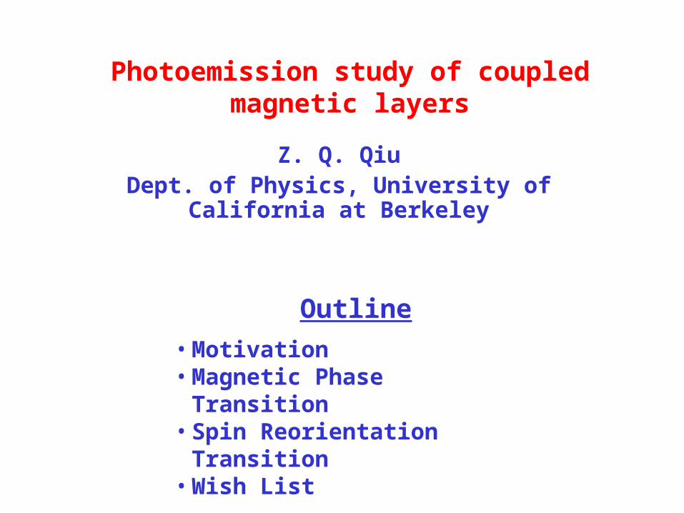
Photoemission study of coupled magnetic layers Z. Q. Qiu Dept. of Physics, University of California at Berkeley Outline • Motivation • Magnetic Phase Transition • Spin Reorientation Transition • Wish List
-
Upload
jeremy-owen -
Category
Documents
-
view
215 -
download
1
Transcript of Photoemission study of coupled magnetic layers Z. Q. Qiu Dept. of Physics, University of California...
Photoemission study of coupled magnetic layers
Z. Q. QiuDept. of Physics, University of California at Berkeley
Outline
• Motivation• Magnetic Phase Transition• Spin Reorientation Transition• Wish List

2D 0D1D
Motivation
GMR and Oscillatory Coupling• P. Grünberg, et. al., Phys. Rev. Lett. 57, 2442 (1986).• M. N. Baibich, et. al., Phys. Rev. Lett. 61, 2472 (1988).• S. S. P. Parkin et. al. Phys. Rev. Lett. 64, 2304 (1990).
5ML 3010 15 2520Spectroscopy of valence electrons
• How does the interlayer coupling change the magnetic properties of the individual layer?
Microscopy of core electrons (PEEM)• Element-specificity + imaging

What is effect of the interlayer coupling on the phase transition?•
Single or separate phase transitions?
•
How is the TC of the coupled sandwich compared to TC1 and TC2?
Magnetic Phase Transition
FM2
FM1FM1 FM2
TC1 TC2
?
Co
Ni
T=310K 380K 430K
Ni(3ML)/Fe(5ML)/Co(10ML)/Cu(100)
Ni
Co
dc
Ni(wedge)/Fe(5ML)/Co(10ML)/Cu(100)

Co(0.23ML)/Cu(2ML)/Ni/Cu(100)
Ni
0.23ML
5.3ML 5.8ML 6.2ML 7.1ML4.9ML
Co
dNi =
dCo= 0.23ML 0.23ML0.23ML 0.23ML
Co(2.3ML)/Cu(2ML)/Ni/Cu(100)
Ni
2.3ML
3.4ML 4.1ML 5.3ML 7.5ML
Co
dNi =2.5ML
dCo= 2.3ML 2.3ML 2.3ML 2.3ML
Co(1.3ML)/Cu(2ML)/Ni/Cu(100)
dCo=
Ni
3.7ML
Co
dNi =
1.3ML
4.5ML 5.0ML 5.4ML 6.1ML
1.3ML 1.3ML 1.3ML 1.3ML

0 1 20
1
2
3
4
5
6
7
IV
III
II
I
Ni thickness(ML)
Co thickness (ML)
Co Ni
0 1 20
1
2
3
4
5
6
7
IVII
IIINi thickness (ML)
Co thickness (ML)
Co Ni
I
Co/Cu(2ML)/Ni/Cu(100) Co/Fe(5ML)/Ni/Cu(100)
I II III IV
Ni PM FM PM FM
Co PM PM FM FM
• PM state of one layer has little effect on the Tc of the other film.
• FM state of one layer reduces the dc of the other layer.

dCo
dNi
I1: PM2: PM
II1: PM2: FM
IV1: FM2: FM
III1: FM2: PM
Jint=0 Jint0
dCo
dNi
I1: PM2: PM
II1: PM2: FM
IV1: FM2: FM
III1: FM2: PM
4.0 5.0 6.0 7.0 8.0 9.01.0
2.0
3.0
4.0 FCAFC
Cu/Co(3ML)/Fe/Ni/Cu(100) Cu/Co(1.6ML)/Fe/Ni/Cu(100) Cu/Co(1ML)/Fe/Ni/Cu(100)
Ni thickness (ML)
Fe thickness (ML)
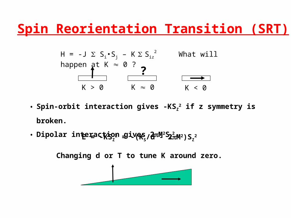
Spin Reorientation Transition (SRT)
H = -J Si•Sj – K Siz2 What will happen at K 0 ?
K > 0 K < 0K 0
?
• Spin-orbit interaction gives -KSZ2 if z symmetry is broken.
• Dipolar interaction gives 2M2SZ2.
E = -KSZ2 = -(KS/d - 2M2)SZ
2
Changing d or T to tune K around zero.
• Electron Microscope can be used to study stripe domains as a function of “magnetic field”.
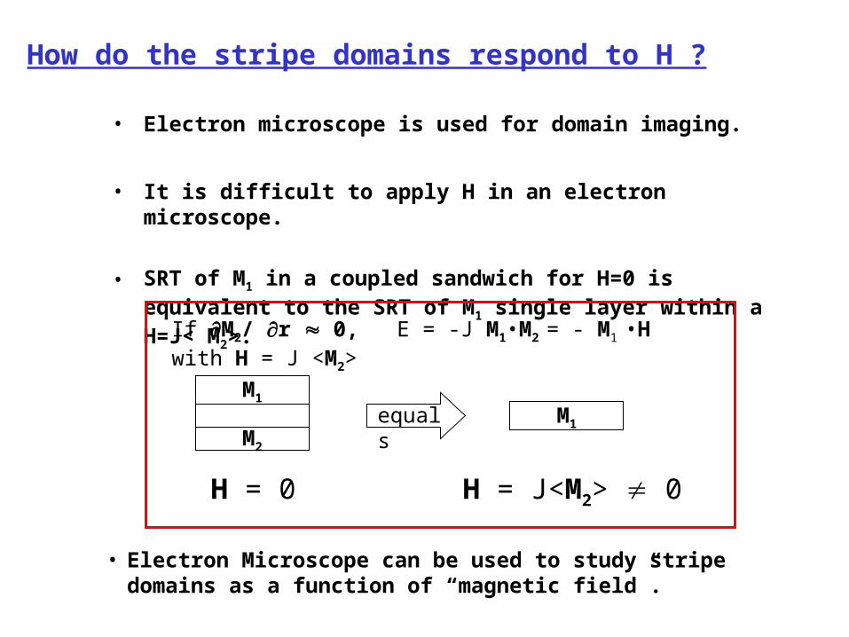
M1
M2
If M2/ r 0, E = -J M1•M2 = - M1 •H with H = J <M2>
H = 0
M1
H = J<M2> 0
equals
How do the stripe domains respond to H ?
• Electron microscope is used for domain imaging.
• It is difficult to apply H in an electron microscope.
• SRT of M1 in a coupled sandwich for H=0 is equivalent to the SRT of M1 single layer within a H=J< M2>.

• Sample is grown by MBE.
• Fe/Ni(5ML) film as the SRT layer.
• Cu/Co(10ML) provides the in-plane magnetic field.
Cu(001)
Fe/Ni
H = JMCo
Co
Cu

2.3 2.4 2.5 2.6 2.70
1
2
3
4
5
6
Domain width (
μ)m
( )Fe thickness ML
2.4ML
(c)
2.6ML 2.8ML
50μm //(a)
(b)10μm
Fe thickness (ML)
15μm
Co Fe
15μm
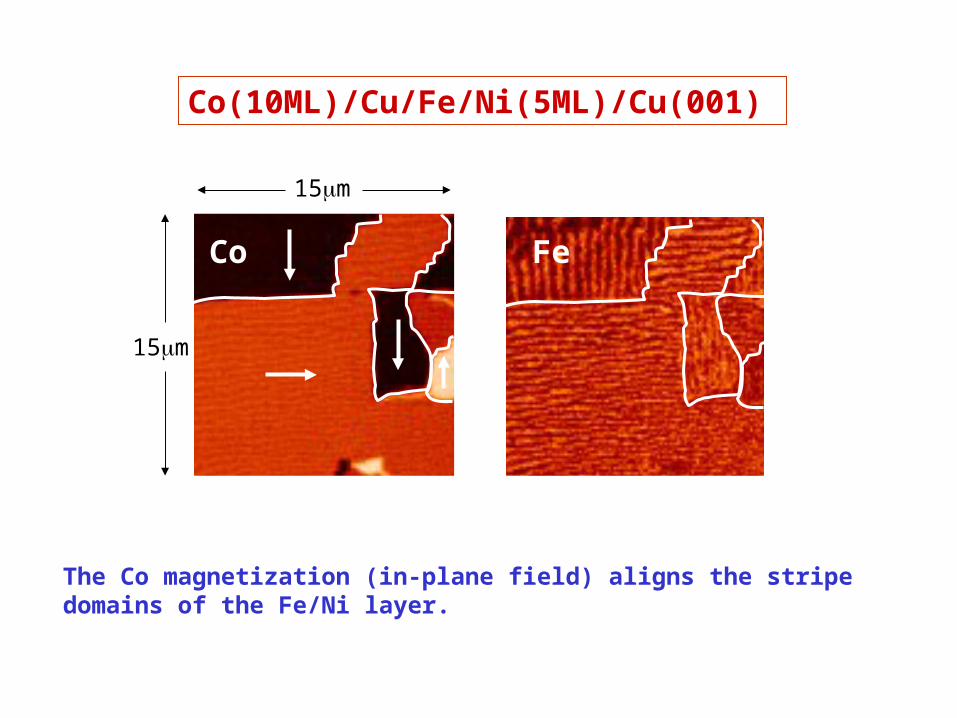
Co(10ML)/Cu/Fe/Ni(5ML)/Cu(001)
The Co magnetization (in-plane field) aligns the stripe domains of the Fe/Ni layer.

Co(10ML)/Cu/Fe/Ni(5ML)/Cu(001)
6.3ML
6.9ML
dFe(ML)
dCu(ML)
FC
AFC
2.84ML2.44ML
50μm
H
K

dFe=2.53ML 2.59ML 2.66ML 2.72ML
dCu=6.57ML 6.66ML 6.73ML 6.81ML
6.47ML 6.38ML 6.27MLdCu=6.57ML
(a)
(b)
(c)

w
w
L
z
y
x
μH=Jint
Ω−≈Ω
+Ω−≡ KJ
KKe 4
2
π

( )1/
1/exp
6
524
242
+Ω
+Ω⋅
Ω=
e
e
KJ
KJJL
π
ππ
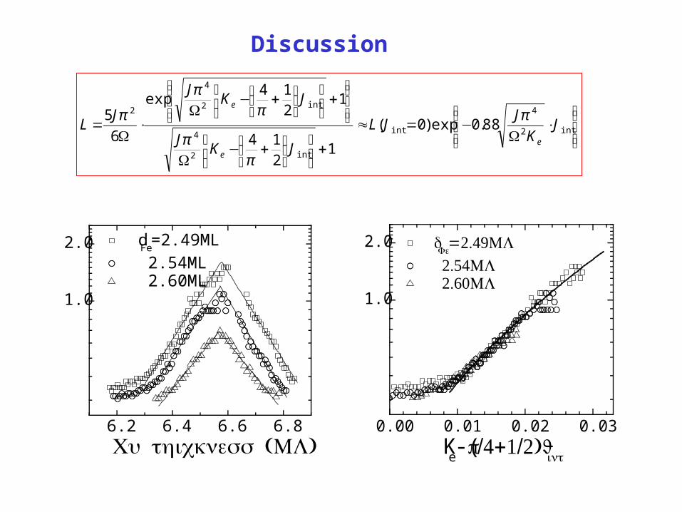
Discussion of Jint=0.
2.3 2.4 2.5 2.6 2.70
1
2
3
4
5
6
Domain width (
μ)m
( )Fe thickness ML
2.4ML
(c)
2.6ML 2.8ML
50μm //(a)
(b)10μm
Fe thickness (ML)
⎪⎭
⎪⎬⎫
⎪⎩
⎪⎨⎧
⋅Ω
−=≈
+⎥⎦
⎤⎢⎣
⎡⎟⎠⎞
⎜⎝⎛ +−
Ω
⎪⎭
⎪⎬⎫
⎪⎩
⎪⎨⎧
+⎥⎦
⎤⎢⎣
⎡⎟⎠⎞
⎜⎝⎛ +−
Ω⋅
Ω= int2
4
int
int2
4
int2
4
2
88.0exp)0(
12
14
12
14exp
6
5J
K
JJL
JKJ
JKJ
JL
e
e
e
π
π
π
π
π
π
Discussion
6.2 6.4 6.6 6.8
1.0
2.0 dFe
=2.49ML
2.54ML 2.60ML
Domain width (
μ)m
( )Cu thickness ML0.00 0.01 0.02 0.03
1.0
2.0
Ke-(/4+1/2)Jint
dFe=2.49ML
2.54ML 2.60ML
(Domain width
μ)m

• Keep pushing the spatial resolution down to nm for laterally modulated structures (vicinal surfaces, wires, and dots …).
• Element-specific measurement of antiferromagnetic materials other than oxides (Mn, Cr, FeMn).
• Microscopy within magnetic field.
• Fast spin Dynamics (t<1-10ps).
• Improve in-situ sample preparation capability.
Wish List
1. Develop techniques that are unique for certain type of problems (e.g., element-specificity).
2. Attract users who are doing outstanding research on magnetic nanostructures, but not yet using synchrotrons.

• Department of Physics, University of California at Berkeley Y. Z. Wu, C. Won, and H. W. Zhao
• Advanced Light Source, Lawrence Berkeley National Laboratory A. Doran and A. Scholl
• Department of Physics, Fudan University X. F. Jin
Collaborators