SHG7210/97 Philips หูฟังสำหรับเล่นเกมคอมพิวเตอร์ · Philips หูฟังสำหรับเล่นเกมคอมพิว

PHILIPS
PM 3347 SWEEP DELAY TIME BASE
9499 440 05211 1/668/1/02/03

3
IMPORTANT
In correspondence concerning this apparatus, please quote the type number and the serial number as given on the type plate at the rear o f the apparatus.

4
Contents
GENERAL INFORMATION
I. Introduction 5
IX. Mode selector switch
X. Gated working of Time-base A
15
20
II. Technical data 6 XI. Trigger Circuit 21
III. Description of the block diagram 8 XII. Checking and Adjusting 26
A. General Information 26
DIRECTIONS FOR USE B. Time-base and Triggering 26
IV. Installation 9 C. Delay 28
V. Functions of the controls 10 D. Output Terminals 29
VI. Applications 11
SERVICE NOTES XIII. Parts list 30
VII. Time base B 13 A. Mechanical 30
VIII. Delay pick-off Circuit 13 B. Electrical 31
List of figures
Fig. Page Fig. Page
1 Survey of the controls 8 14 Generation of the intensifying pulse 17 2 X-deflection 10 15 Mode selector switch SK7 at 3 Time-base B 10 "A delayed by B" 18 4a "B" intensified by "A" 10 16 Generation of the delayed Time base A 19 4b "A" delayed by "B" 10 17 Gated working of "A delayed by B" 20 5 Calculating the delay time 10 18 Trigger Circuit 23 6 Example of a display 11 19 Right-hand side 24 7 Measuring time "T" 11 20 Left-hand side 24 8 Time jitter 12 21 Front view 25 9 Voltage comparator circuit 12 22 Delay unit; unit 5 33 10 Schmitt-trigger, 23 Time-base unit; unit 6 36
differentiator and cathode follower 13 24 Delay circuit 41 11 Generation of the delayed trigger pulse 14 25 Time coefficient switch 45 12 Mode selector switch SK7 at ".Time-base B" 15 26 Time- base generator circuit 49 13 Mode selector switch SK7 at
"B" intensified by "A" 16
5
GENERAL INFORMATION
Introduction O The PM 3347 is a trigger-delay plug-in unit for the basic oscilloscope PM 3330. The unit can supply a sawtooth voltage for X-deflection (TIME-BASE B) as well as a delayed trigger pulse. With this pulse, the time-base generator of the basic oscilloscope (TIME-BASE A) can be started.
Using this operating method, a selected part of the display can be magnified across the entire screen-width so that accurate measurements are possible.
Moreover, possible time-jitter in the magnified display can be eliminated.
6
Technical data
Properties, expressed in numerical values with state-
ment of tolerances are guaranteed by the factory.
Numerical values without tolerances are intended for
information purposes only and indicate the properties
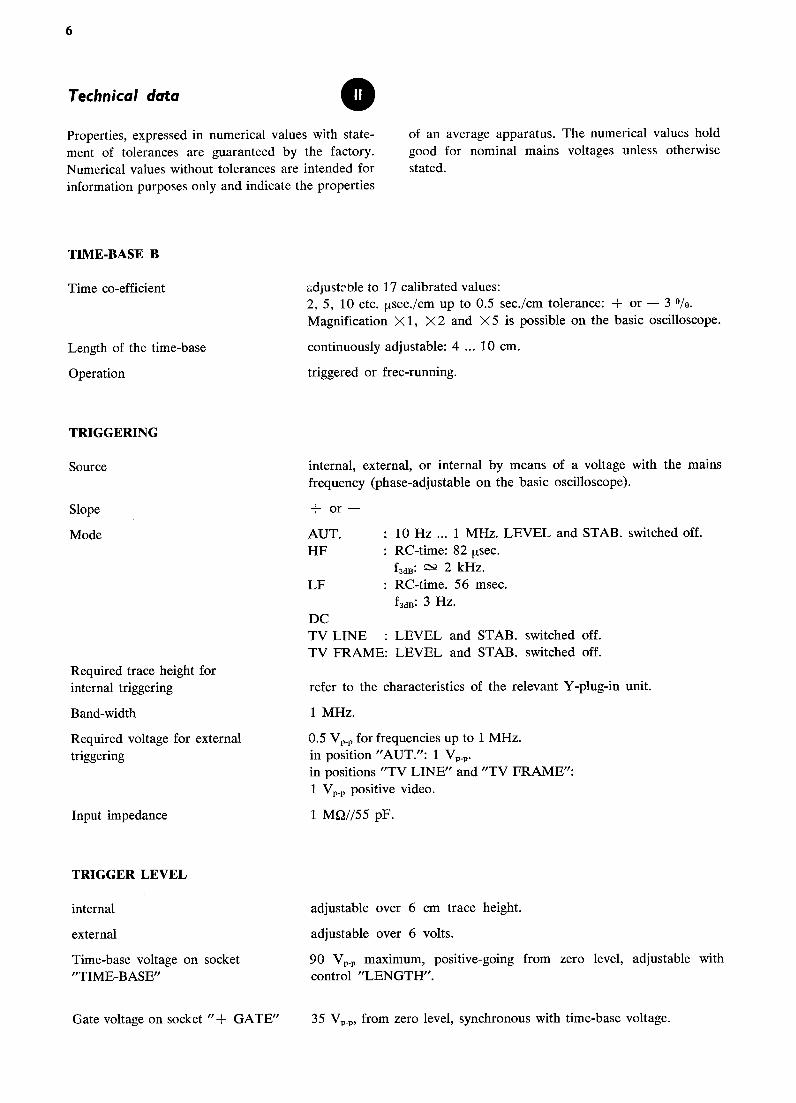
TIME-BASE B
Time co-efficient
Length of the time-base
Operation
TRIGGERING
Source
Slope
Mode
Required trace height for internal triggering
Band-width
Required voltage for external triggering
Input impedance
TRIGGER LEVEL
internal
external
Time-base voltage on socket
"TIME-BASE"
of an average apparatus. The numerical values hold
good for nominal mains voltages unless otherwise
stated.
adlustable to 17 calibrated values: 2, 5, 10 etc. µsec./cm up to 0.5 sec./cm tolerance: -i- or — 3 0/0. Magnification X 1, X 2 and X 5 is possible on the basic oscilloscope.
continuously adjustable: 4 ... 10 cm.
triggered or free-running.
internal, external, or internal by means of a voltage with the mains
frequency (phase-adjustable on the basic oscilloscope).
-I-- or —
AUT. HF
LF
10 Hz ... 1 MHz. LEVEL and STAB. switched off. RC-time: 82 µsec. f3dB: N 2 kHz. RC-time. 56 msec.
fsas: 3 Hz. DC TV LINE :LEVEL and STAB. switched off. TV FRAME: LEVEL and STAB. switched off.
refer to the characteristics of the relevant Y-plug-in unit.
1 MHz.
0.5 Vp_p for frequencies up to 1 MHz. in position "AUT.": 1 VP_P. in positions "TV LII~TE" and "TV FRAME": 1 VP_P positive video.
1 MSz//55 pF.
adjustable over 6 cm trace height.
adjustable over 6 volts.
90 Vp_P maximum., positive-going control "LENGTH".
from zero level, adjustable with
Gate voltage on socket "-~ GATE" 35 VP_P, from zero level, synchronous with time-base voltage.

7
DELAY PULSE
Delay 2 µsec. — 5 s, continuously adjustable by means of a 17 step-switch (accuracy 3 0/0 of the front-plate value, ± 200 nsec.) and a helical potentiometer (0.2 ~/o of the final value).
Jitter ~ 1 :20.000
Output voltage on socket "DEL'D TRIGG."
Mechanical data
3 VP-P
By means of the delay pulse, time-base A can optionally be directly started (STARTS A), or, released but not started (SETS A READY). In this case, time-base A is started by the next trigger pulse.
width : 15 cm depth : 30 cm (knobs and plug included) height : 18 cm weight: 2 kg
Accessories Manual
8
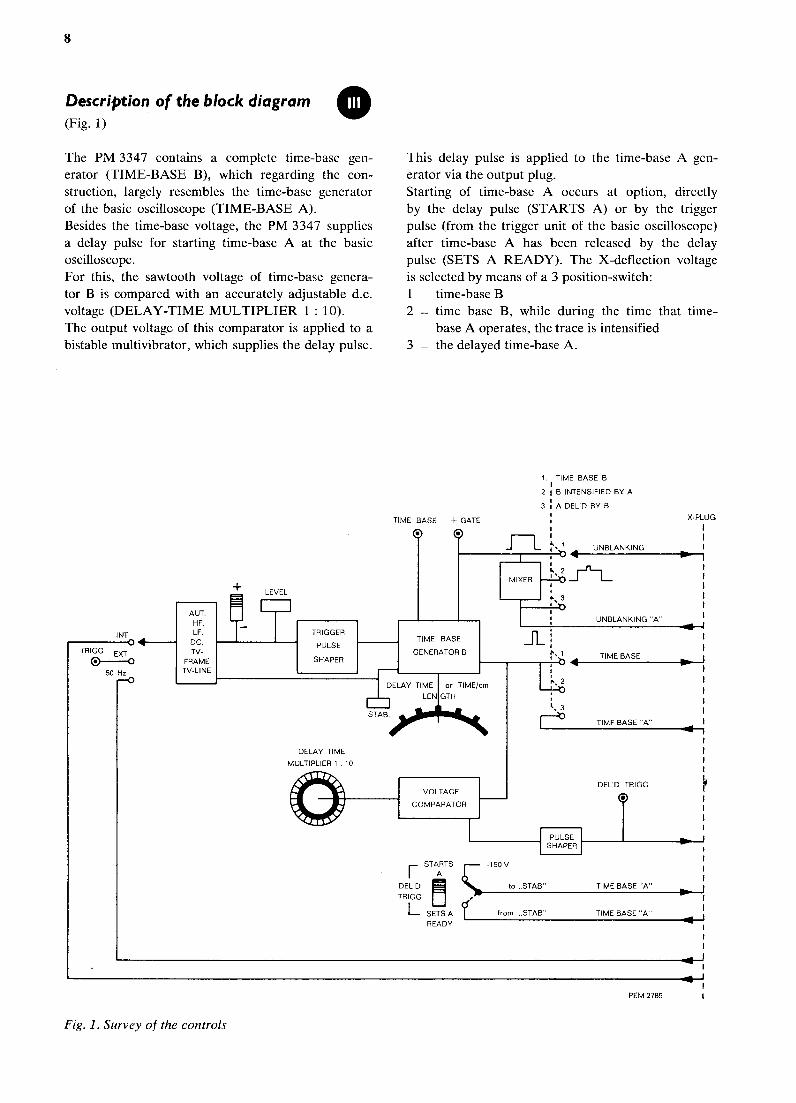
Description of the block diagram (Fig. I )
The PM 3347 contains a complete time-base gen-erator (TIME-BASE B), which regarding the con-struction, largely resembles the time-base generator of the basic oscilloscope (TIME-BASE A). Besides the time-base voltage, the PM 3347 supplies a delay pulse for starting time-base A at the basic oscilloscope. For this, the sawtooth voltage of time-base genera-tor B is compared with an accurately adjustable d.c. voltage (DELAY-TIME MULTIPLIER 1 : 10). The output voltage of this comparator is applied to a bistable multivibrator, which supplies the delay pulse.
INT
TRIGG EXT
50 Hz
~—
AUT. H F. LF.
DC. Tv-
FRAME TV-LINE
LEVEL
Fig. 1. Survey of the controls
TRIGGER
PULSE
SHAPER
This delay pulse is applied to the time-base A gen-erator via the output plug. Starting of time-base A occurs at option, directly by the delay pulse (STARTS A) or by the trigger pulse (from the trigger unit of the basic oscilloscope) after time-base A has been released by the delay pulse (SETS A READY). The X-deflection voltage is selected by means of a 3position-switch: 1 —time-base B 2 —time base B, while during the time that time-
base Aoperates, the trace is intensified 3 —the delayed time-base A.
TIME BASE +GATE
~' 0
1. TIME BASE B I
2. I B INTENSIFIED BV A
3. iADEL'D BYB I
I I
J L ~ ~ ~b
DELAY TIME
MULTIPLIER 1 : 10
TIME BASE
GENERATOR B
MIXER 4 2
'~n i
3
X-PLUG 1
UNBLANKING
UNBLANKING "A"
DELAY TIME or TIME/cm
LEN GTH
STAB.
VOLTAGE
COMPARATOR
TIME BASE
TIME BASE "A"
r STARTS R— -150 V
I A DEL'D TRIGG
L SETS A READY
PULSE SHAPER
DEL'D TRIGG
Q
to „STAB" TIME BASE "A"
from „STAB" TIME BASE "A"
PEM 2785

9
DIRECTIONS FOR USE
Installation m The PM 3347 should be plugged into the right-
hand side plug-in compartment of basic oscilloscope
PM 3330 (X-UNIT). Switching-on is effected via the mains switch of the
basic oscilloscope.
BU1: BU2: BU3: BU4: BUS: R1
R2
R3
R4
Input for external triggering Output with the pos. sweep gating signal
Output with the time base "B" signal
Output with the delayed triggering signal
Earthing bush Sweeplength control Trigger level control Trigger stability control Trigger delay time control
If the PM 3347 is used, the deflection switch in the
X-DEFLECTION frame of the PM 3330 should be
put into position "X-UNIT".
r~ $U 5
SKI: Triggering mode selector SK2: Triggering slope selector
SK3: Triggering source selector SK4: Selector of the X-deflection co-efficient
or the trigger delay time (coarse)
SKS: Preset trigger stability switch
SK6: Start/release selector for time base "A"
SK7: X-deflection mode selector. Remark: At the picture, R2 and R3 were interchanged.

10
Controls and their functions
X-DEFLECTION
0 The X-deflection voltage is selected by means of the 3-position switch on the right-hand lower-side of the unit.
Time base B
The X-deflection voltage is then supplied by time-base generator B. Adjustment of time-base B is effected in the same way as described for time-base A, in the manual of the basic oscilloscope. The time co-efficient of time-base B can only be adjusted in steps. The length of the time-base can be adjusted by means of the "LENGTH" control. The time co-efficients are not influenced by this control.
B Intensified by A
In this position also, the X-deflection voltage is sup-plied by time-base generator B. When switch "DEL'D TRIGG." is in position: "STARTS A", the brightness-control voltage of time-base Atogether with that of time-base B will be applied to the Wehnelt cylinder of the CRT. Consequently, the trace will be intensified during the running of time-base A. By means of this indication, that part of the trace can be selected, which must be examined in detail.
When using the PM 3347 as a trigger-delay unit, the trigger-mode switch of the basic oscilloscope may be in any position but "AUT.".
A Delayed by B
In this position, time-base generator A supplies the deflection voltage. Time-base A is started in the same way as in position "B INTENSIFIED BY A". This means that the part of the trace which was
intensified, is then displayed across the entire screen-width.
ADJUSTING THE DELAY
If the PM 3347 is used as a trigger-delay unit, the deflection switch should be set to position "B IN-TENSIFIED BY A", to adjust the delay. Time-base B is adjusted in the normal way by means
of the controls in the "TIME-BASE B" frame.
Fig. 2. X-Deflection
Fig. 3. Time-base B
Fig. 4a. B intensified by A
J
Fig. 4b. A delayed by B
L
r
DECAY tltA
,. ' ~y A
TIhhE,rfm
~c
s
DElgy ~""+..
MUITIPIIER ~ip
Fig. S. Calculating the delay time

11
If switch "DEL'D TRIGG." is in position "STARTS
A" (this means that time-base A is triggered by the
delay pulse), the delay time will be equal to the
product of the values indicated by knobs "DELAY
TIME" and "DELAY TIME MULTIPLIER". In
Fig. 5 the delay time amounts to: 3.86 X 50 µsec. = 193 µsec.
The magnitude of the intensified part of the trace
depends on the time co-efficient of time-base A and
should consequently be adjusted by means of knob
"TIME/cm" on the basic oscilloscope. If switch "DEL'D TRIGG." is in position "SETS
A READY", time-base A is released by the delayed
trigger pulse. Time base A will be triggered by the
next pulse, generated at the trigger unit of the basic
oscilloscope.
The adjustment of time-base "A" then is effected in
the same way as with normal use of this time-base
(refer to manual PM 3330) with the restriction that
position "AUT." of the "TRIGGER-MODE" switch
may not be used.
A~~lications
The PM 3347 is particularly used when details of a
complicated, periodical signal are to be measured.
Assume that the display (Fig. 6) is obtained in posi-
tion "TIME-BASE B" of the deflection switch on the
PM 3347. Time-base B is then triggered by the clock-pulse, by
which the pattern is always started.
In this example the clock-pulse has a higher amplitude
than the other pulses. Consequently, the time-base
may be internally triggered. I f all pulses have the same
amplitude, no stable display is obtained with internal
triggering. In that case the time-base should be trig-
gered by an external voltage.
When pulse P is to be accurately measured, the
deflection switch should be set to position "B IN-
TENSIFIED BY A" and switch "DEL'D TRIGG."
should be set to position "STARTS A".
With aid of control "DELAY-TIME MULTIPLIER"
and switch "TIME/cm" of the basic oscilloscope,
part P of the display is intensified.
When the deflection switch is then set to position "A
DEL'D BY B", the intensified part (magnified across
the entire screen) is reproduced.
In this position, pulse-width, rise-time etc. can be
accurately measured by means of the calibrated time
coefficients of time-base A.
The time T (delay time of pulse P with respect to
the clock-pulse) can be measured by adjusting knob
The adjusted value of the delay time is then increased
by an additional time, which depends on the trigger
signal of the basic oscilloscope. Consequently, the
adjusted value of the knobs on the PM 3347 no
longer applies.
LENGTH
If long delay times are used (time-coefficient of
time-base A much smaller than the time coefficient
of time-base B), time-base A will have a very short
duty cycle. This means that the brightness of the
trace in position "A DEL'D BY B" is very low with
respect to the other positions.
By adjusting the length of the time-base in the posi-
tion "B INTENSIFIED BY A", so that the intensified
part of the trace just remains present, the repetition
frequency of time-base B can be increased in many
cases. Consequently, the repetition frequency of time-base
A is increased and the luminosity increases also.
"DELAY-TIME MULTIPLIER" so, that the lead-
ing edge of pulse P just coincides with the beginning
of the time-base.
T is equal to the product of the values indicated by
knobs "DELAY TIME MULTIPLIER" and "DE-
LAY-TIME".
f l Fig. 6. Example of a display
K T
P --•, ~.-
P
1
Fig. 7. Measuring time "T"

12
TIME JITTER The delay time, however, can in this case no longer be read in the above mentioned way.
Possible time jitter of pulse P with respect to the clock-pulse causes a haze and can be measured in the position "A DEL'D BY B" by means of the cal-ibrated time co-efficients of time-base A. (Fig. 8). If the measurements are impeded by time jitter, the latter can be eliminated by setting switch "DEL'D TRIGG." to position "SETS A READY" and by adjusting the controls of time-base A so, that time-base A is triggered.
+200V
813
,'_=-_~~ R116
R98 Miller Circt
+130V
-150V
Fig. 9. Voltage comparator circuit
B16p
R123
-150V
--~ ~~-ptter
Fig. 8. Time jitter
Delayed Trigger
~L Multivibrator
R129 ► R 134
814
-150V
R4
Max.Delay
"Delayt i me" Multiplier 1-10
Min. Delay
R132
+330V
PEM 2877
eta
819
Remark: The cathode of B 19 is earthed

13
SERVICE NOTES
Time base B
This plug-in unit comprises a complete time-base generator, a trigger unit and adelay-pick-off circuit. The delay-pick-off circuit delivers a pulse, after an adjustable delay, to front-panel socket BU4 and to time-base A for delayed triggering (see Fig. 1). Time-base B, like time-base A, is based on a Miller run-up circuit with the following modifications:
Delay pick-o f f circuit
Valves B13, B14 and B16p constitute along-tailed pair circuit (Fig. 9) which acts as a voltage com-parator. In the quiescent state of the voltage comparator, B13 is cut off and the cathode voltage of B14 is approximately equal to the voltage applied to the grid of B 14 from helical potentiometer (R4) "Delay time-multiplier 1-10". The range of R4 is preset by means of potentiometers R129 and R132. The ramp voltage from the output of time-base B is applied to the grid of B13, which will start to conduct when its cut-off voltage is reached. However as B 16p is aconstant-current source, sup-
1~
814a
+330`J
Schmitt -trigger
+130v
— the "Sweep-length" control is no longer a preset adjustment, but afront-panel control "Length". Continuous sweep speed control is not possible.
— the lock-out multivibrator (single-shot facility) is not duplicated.
The working of the time-base generator is not de-scribed due to its similarity with that of time-base A.
plying the cathodes of both B13 and B14, a rise in current through one (B13) will cause an equal drop in current through the other (B14). Furthermore, the use of a constant current source in their cathodes makes the current in B14 independent of the setting of R4 (the "Delay-time Multiplier 1-10"), which is used to determine the point at which the take-over
of current by B 13 from B 14 occurs. In this way the output from B14 to the Schmitt trigger starts from a constant level and provides a constant amplitude step. The voltage rise of the anode of B14 is applied to the Schmitt trigger circuit, (Delayed trigger multivibrator) consisting of valves B17' and B17". (Fig. 10). In the quiescent state B 17' is cut-off and B 17" is
+130V
Bl6t
Del d trigg BU4
20 BUX Del ~ t ri gg time -base A
Differentiator Cathode follower
Fig. 10. Schmitt-Trigger, Dif ferentiator and Cathode follower
FIG 3 PEM 2872

14
conductive. When the anode-voltage of B14, applied to the grid of B 17', rises above the switching level of the Schmitt trigger, the circuit switches over: B 17' conductive and B 17" cut-off. The anode voltage of B17" therefore rises abruptly. When the ramp-voltage drops below the cut-off level of B13 (during the fly-back interval) the anode volt-age of B 17" returns to the quiescent value. Thus a rectangular voltage wave-form is produced at the anode of B 17". This voltage waveform is differentiated by capacitor C59 and resistor R143//R144, so that positive and negative spikes appear at the grid of trigger-amplifier valve B 16t. With no input signal present, B16t is biased beyond
cut-off and the positive spikes cause it to become conductive, thus producing positive output spikes at the cathode. The negative spikes theoretically do not appear at the output; however, some effect may be evident in the output signal, see Fig. 11.
Thus, after time base B has been triggered, there follows a certain pre-determined time-delay before time base A can operate. The trigger pulse is also available at the socket "DELAYED TRIGG.". This delay can be set with controls "DELAY - TIME or TIME/cm" and "DELAY TIME MULTIPLIER 1-10" and the actual time interval is the product of these two settings.
T= ~Time~cm setting X ~~Delay time multiplier~~setting
V/B 13 g
200V
814a
330 V 817 a
r T
~ tugger point
B16t g -~
B 16 t c --~
Fig. 11. Generation of the delayed trigger pulse
BT3 14 Cathode level set bid R 4
Schmitt trigger switching level
Output of Schmit! trigger
Differentiated rectangular waveform
Output at Socket "Deli D trigger"
PEM 2895

15
Mode selector switch SK7
A. AT "TIME BASE B"
When the X-deflection switch on the main frame is at "X UNIT"* and switch SK17 on the time-base B unit at "TIME BASE B", the complete function of time-base A is taken over by time-base B. The relevant interconnections are as shown in Fig. 12.
Y-UNIT
TRIGGER CIRCUIT
TIME BASE~~B~~
0
I I
TIME BASE.B
DELAY CIRCUIT
SK7
I I SK710 I ~.' O
Time-base B provides the unblanking pulse via 8 BUX. The output of Miller circuit B drives the hori-zontal amplifier in the basic oscilloscope and the delay circuit.
eu x
X-AMPL.
10
017
2
Y (TRIGGER UNIT► CIRCUIT
Starts ';C"lO O SK6 31
Sets'A"ready o 015 ~ STAB.CONTROL
24
TIME BASE. A
Fig. 12. Mode selector switch SK7 at "Time-base B"
RESET CIRCUIT
PEM 2876
16
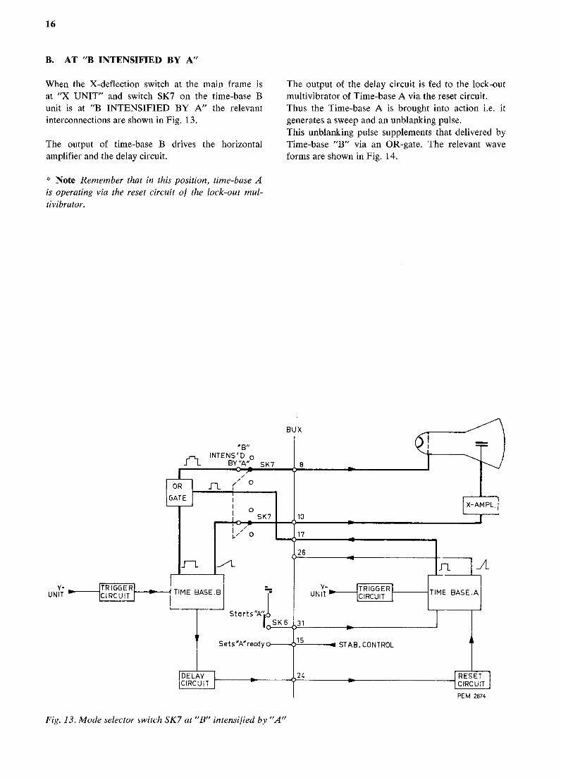
B. AT "B INTENSIFIED BY A"
When the X-deflection switch at the main frame is at "X UNIT" and switch SK7 on the time-base B unit is at "B INTENSIFIED BY A" the relevant interconnections are shown in Fig. 13.
The output of time-base B drives the horizontal amplifier and the delay circuit.
Note Remember that in this position, time-base A is operating via the reset circuit of the lock-out mul-tivibrator.
Y-UNIT
TR IGGE R CIRCUIT
> B/I
INTENS'D O BY"A"
~~ O OR
GATE
SK7
The output of the delay circuit is fed to the lock-out multivibrator of Time-base A via the reset circuit. Thus the Time-base A is brought into action i.e. it generates a sweep and an unblanking pulse. This unblanking pulse supplements that delivered by Time-base "B" via an OR-gate. The relevant wave forms are shown in Fig. 14.
BUX
TIME BASE.B
L DELAY CIRCUIT
10
X-AMPL
17
2
Y-UNIT
Starts'A" ~O SK6 3
TRIGGER CIRCUIT
JL
Sets"A"readyo 015 ~ STAB,CONTROL
2
TIME BASE.AI
Fig. 13. Mode selector switch SK7 at "B" intensified by "A"
RESET CIRCUIT
PEM 2874

17
Time T -Delay time X delay time multiplier"
d. c. level of Delay time multiplier setting
T ~ T~ r
I
1
r-~ I ~
_~ L, Displayed waveform
(shown full line)
i I I
J
f
1
Fig. 14. Generation o f the intensifying pulse
F
Ramp output of
time base $
Unblanking waveform time base B
Delay circuit utput pulse
Ramp output of time-base "A
~~
Unblanking waveform time base "A''
Combined Unblanking waveform
~~Starts A~~
Del. trigg. PEM 2898

18
C. AT "A DEL'D BY B"
When the X-deflection is at "X-UNIT" and switch SK7 on unit time-base B is at "A DEL'D BY B", the relevant interconnections are as shown in Fig. 15. Unblanking is provided only by Time-base "A".
The horizontal amplifier is driven from Time base A.
UN T ~ TRIGGER CIRCUIT
p." DEL'D o SK 7
BY "B'i~
I i
TIME BASE B
DELAY CIRCUIT
I ~
I SK7d,
The output from the delay circuit is fed to the lock-out multivibrator of Time base A via the reset circuit.
The portion of the display that was intensified in the previous position of SK7 is now expanded horizontal-ly to occupy the entire screen width (Fig. 16).
Bux
1
2
X-AMPL.
_ Y- TRIGGER UNIT ~ CIRCUIT
Starts~A" o SK6 31 ~
Sets'G,"ready o 1
26
~ STAB. CONTROL
TIME BASE A
Fig. 1 S. Mode selector switch SK7 at "A delayed by B"
RESET CIRCUIT
PEM 2875

19
T ~ T'
r - ~ r - ~ r r - ~ r - ~ I ( I I I I I I 1 i L_J L_J I I L_J L
d. c. level of I Delay time ~ multiplier setting
'" Starts A"
Del.trigg~
Fig. 16. Generation of the delayed time base A
Displayd waveform T' ( shown full line )
Ramp output of time -base "B"
Delay circuit output pulse
Ramp output of time-base '~A""
Unblanking waveform time -base "A"~
PEM 2893

20
Gated working o f Time-Base A
If SK6 is set to "STARTS A", the input of the S.G.M.V. of the Time-base A circuit is set below the lower hysteresis limit so that the time-base generator will start, regardless of the setting of the "Stab." control.
Thus when the delay pulse triggers Time-base A, the sweep starts immediately, see Fig. 14. If SK6 is set to "SETS A READY", the "STAB." control in Time-base A becomes operative so that
T
Trigger pulse for time baseB.l I r ,,,l r , I_,ILevel set to trigg. on higher) amplitude pulse
_,
-7I I I I I I l.. _ J L J t_ J I~- _
d•c. level of I Delay time —multiplier setting
Stability level time base A S.g.m.v. hysteresis
gap
Trigger pulse ~ from trigger
unit A
the S.G.M.V. input d.c. level can be set for triggered operation.
Thus, when the delay pulse triggers the lock-out multivibrator, the output of the latter is not sufficient to exceed the S.G.M.V. lower hysteresis limit.
The arrival of a further pulse from the trigger cir-cuit Awill therefore cause this hysteresis limit to be exceeded so that the Time-base A is locked to this pulse (Fig. 17).
T ~
I
r 1 Displayed waveform T" _ _J ` (shown full line
I
Ramp output of time -baste "B'~
Delay circuit output pulse
Lock out m. v, output of time -base A~
Ramp output of time base ;q"
Unblanking waveform time base "'A"
Del.trigg.
"Sets A ready"
Fig. l7. Gated working of "A delayed by B"
PEM 2894
21
Trigger circuit m
Compared with trigger unit A of the basic oscil-loscope this trigger circuit is of a simpler design in that the trigger amplifier consists of along-tailed pair circuit and the pulse shaper is aSchmitt-trigger. (Fig. 18) The source selection, slope selection and mode selec-tion as well as the TV synchronisation separator are identical to the ones of the basic oscilloscope (also see Fig. 43 and Fig. 44 of the basic oscilloscope). The trigger signal can be derived from either the Y-deflection signal or the mains supply (via 27BU-X). In the first case the trigger signal is applied sym-metrically to trigger amplifier B1'—B1"; in the two latter cases it is applied asymmetrically. The am-plified signal is routed from the anode of B1' to the Schmitt-trigger. The latter switches when the applied signal reaches a certain level. Thus, a square wave originates at the anode of B3" which is differentiated by'the C24—R66 network.
The resulting negative spikes will switch over the S.G.M.V. (B4"—B6') to start the time base generator, but the positive spikes are suppressed by diode GR7 to prevent undue resetting of the S.G.M.V. The level at which the Schmitt-trigger will operate is set by potentiometer R59 "Trigger Sens". The moment at which the trigger signal will reach that level depends on the d.c. potential at the B1" con-trol grid. When mode-switch SK1 is in position "DC", "LF" and "HF" this potential can be varied by means of "Level" potentiometer R2. In the "TV. Line" and "TV. Frame" positions this potential is determined by voltage divider R41 and R42; in the position "Aut.", the control grid is earthed via R43. The polarity of the trigger signal can be selected with switch SK2.
The mode of operation of the time-base generator is determined by the potential at the S.G.M.V. control grid (B4") i.e. the free-running operation or the triggered operation.
When switch SK1 is in the "DC", "LF" or "HF" position, the potential can be varied with "Stab." potentiometer R3. If the potential is low enough to underpass the S.G.M.V. lower hysteresis level the free-running mode of operation is obtained; otherwise the triggered mode of operation is obtained. When the "Stab." control is in the "Preset" position, switch SKS is thrown and the potential of the S.G.M.V. control-grid is determined by the setting of "Preset Stab." potentiometer R113. This also applies to the "TV. Line" and "TV. Frame" position of SK1.
When SK1 is in the "Aut." position, the potential is controlled by the automatic stability control circuit built around B2. If no trigger signal is present, the B2p anode voltage is made low enough to obtain the free-running mode of operation by adjusting the "Aut. Free-run" potentiometer R28. If a trigger signal is present, it is rectified by diodes GR2 and GR3.
A negative voltage then arises at the B2p control grid, which causes the anode potential to rise slightly so that a triggered mode of operation is obtained. The B2p anode voltage is clamped in the positive-going direction by diode GR4 to a d.c. level, present at the cathode of cathode-follower B2t and which is adjusted by "Aut. Trigg. Level" potentiometer R33. This is to keep the time base generator in the trig-gered mode when the amplitude of the trigger signal ahead of the control grid of B2p increases.

23
24BU X~
1sux~ BU1
278U X (SOHz)
lnt
~o SOHz~—.
C
T V Frame oTV Llne
SK1jpCo 0
HF 12
13'
Sync. Sep.
_/L
R39 ' R37
+130V
~R41
R2 Level
SK1
R19
R43
C22
Trigger Ampl. +130 V +200 V
R21 I IR46
C14 GR3
GR2
-150 V
R3 Sta0.
R53
+2o~v ScFmitt- +zo~v Trigger
R54 I R64
1023
►--IR63
B3~ EBBCC
R62 ~ +130 V R57
R61
R65
5
R66
R44 R58
-150 V Preset Stab.
Trigg. Sens.
R24■ ■R26
Aut, Free-run
= 82p EBOCF
R17
R19
-150V
-150V
R109' R1
93° E88CC
82t E80CF
GR4
N R 29
-150 V
C2< R67
Auto-stability-control
R31
Aut. Trigg.Level
R66
R107
-150 V R33
R34
-150 V
PEM 2786
S.G.M.V.
82" E88CC
e4"
811"
Hold-off CIrCUIt
Fig. 18. Trigger Circuit

24
R 33 R 28
R 13 R ~g
Fig. 19. Right-hand side
Fig. 20. Left-hand side
PEM 2835
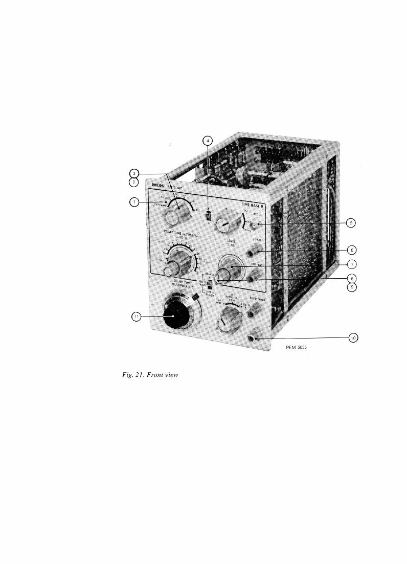
Fig. 2I. Front view

26
Checking and adjusting
A. GENERAL INFORMATION
With the aid of these data, it is possible to carry out all the adjustments of the delay time base PM 3347 and to check the proper working of the plug-in unit. For this, the unit should be inserted into the X-plug-in compartment of acorrectly-adjusted basic oscil-loscope PM 3330. To adjust the time co-efficients and the delay, a number of time-marker signals with accurately known time-intervals is required. For the checking and adjusting of the trigger unit and the time-base generator B, a Y-plug-in unit PM 3333 or another single channel plug-in unit is required. Some of the adjusting elements are on the left-hand side of the unit and are not directly accessible. When these elements must be adjusted, the unit should be connected to the basic oscilloscope via an extension plug (codenumber 4822 263 70009). For a complete adjustment of the instrument the sequence as described in this chapter is to be pre-ferred.
B. TIME BASE B AND TRIGGERING
For the next checking and adjusting points set the below mentioned knobs to the following positions:
Unit PM 3347
"TRIGG. MODE" (SK1) to "H.F." "TRIGG. SOURCE" (SK3) to "INT." SK7 to "TIME BASE B" LENGTH (Rl) clockwise
Basic oscilloscope PM 3330
"X-DEFLECTION" to "X-UNIT" "MAGNIFIER" to "X 1"
1. Stability
— Set "LEVEL" (R2) to its centre position and "STABILITY" (R3) to "PRESET".
— Apply asine-wave voltage with a frequency of 10 kHz to the PM 3333 and adjust the trace height to 3 cm.
— Set "TIME/cm" (SK4) to position " 20 µ.sec./cm" and turn "PRESET STAB." (R113) fully clock-wise.
— Turn R113 so far anti-clockwise that awell-trig-gered display is obtained.
— Check the triggering at different time co-efficients. The time-base generator should not stop and no double trace should be displayed; if necessary, slightly readjust R113.
— Turn "STAB." (R3) fully clockwise; the time-base generator should then be free running.
— When R3 is turned anti-clockwise, a triggered display should be obtained. When R3 is turned still further anti-clockwise while SKS is not yet switched over, the time-base generator should stop and no time-base line should be visible.
2. Trigger sensitivity
— Set "STAB." (R3) to "PRESET". — Switch off the level control by short-circuiting the
cursor of "LEVEL" (R2) to earth. — Apply such a voltage to Y-plug-in unit PM 3333,
that the trace height is 1 mm. The easiest way to obtain this result is to apply the .2 V calibration voltage to the input of the am-plifier, the deflection factor of which has been adjusted to " 2 V/cm".
— Adjust potentiometer "TRIGG. SENS." (R59) for a well-triggered display.
— Remove the earthing connection of the cursor of R2.
3. Trigger slope and level
— Apply asine-wave voltage with a frequency of 10 kHz to Y-plug-in unit PM 3333 and adjust for a trace height of 6 cm.
— Set "TRIGG. SLOPE" (SK2) to position "-{-". The time-base generator should then start on the positive-going edge of the sine wave.
— With "TRIGG. SLOPE" (SK2) to position "—", the time-base generator should start on the nega-tive-going edge.
— It should be possible to shift the starting point continuously over the edge of the sine wave across the entire trace height of 6 cm, by means of "LEVEL" (R2).
— With "LEVEL" (R2) fully clockwise and anti-clockwise, the time-base generator should not operate.
4. Internal triggering
T.V. FRAME
— Set "TRIGG. MODE" (SK1) to "T.V. FRAME" and "TRIGG. SLOPE" (SK2) to "—".

27
— Connect a positive video signal to Y-plug-in unit PM 3333.
— At a minimum trace height of 2 cm, check that a display is obtained, which is triggered on the frame-synchronization pulse. In this case, the trace will start with aframe-syn-chronization pulse.
— In position "T.V. FRAME", "LEVEL" and "STA-BILITY" should have no influence on the display.
T.V. LINE
— Set "TRIGG. MODE" (SK1) to "T.V. LINE" and "TRIGG. SLOPE" (SK2) to "—".
— Apply a positive video signal to Y-plug-in unit PM 3333.
— At a minimum trace height of 2 cm, check that a display is obtained which is triggered on the line-synchronization pulse. In this case the trace will start with aline-syn-chronization pulse.
— In position "T.V. LINE", "LEVEL" and "STA-BILITY" should have no influence on the display.
D.C.
— Set "TRIGG. MODE" (SK1) to "D.C.". — Adjust the time-base generator to its free-running
position and place the time-base line to the centre of the screen with the Y-shift control.
— Apply asine-wave voltage with a frequency of 10 kHz to the Y-plug-in unit and adjust for atrace-height of 3 mm. Set "STAB." (R3) to position "PRESET". Check that after correct adjustment of "LEVEL" (R2), the time-base generator is triggered by the input voltage.
— Increase the trace height to 3 cm. When shifting the trace in vertical direction the starting point of the time-base line should con-tinuously shift across the edge of the sine wave, but stay at the same place on the screen.
L.F.
— Set "TRIGG. MODE" (SK1) to "L.F.". — Apply asine-wave voltage with a frequency of 3 Hz
to plug-in unit PM 3333 and adjust for a trace height of 3 mm.
— Check that after correct adjustment of "LEVEL" (R2), the time-base generator is triggered by the input voltage. "LEVEL" (R2) can easily be preset with a higher frequency of the input signal. The vertical shift on the plug-in unit should have no influence on the trigger level which has been adjusted with "LEVEL" (R2).
H.F.
— Set "TRIGG. MODE" (SKl) to "H.F.". — Apply asine-wave voltage with a frequency of 3 Hz
to plug-in unit PM 3333 and adjust for atrace-height of 1 cm. It should be impossible to trigger the time-base generator with this L.F. voltage.
— Increase the frequency of the input voltage to 2 kHz and 1 MHz resp. and adjust for a trace height of 3 mm. After correct adjustment of "LEVEL" (R2), the time-base generator should be triggered with the input voltage.
AUT.
Set "TRIGG. MODE" (SK1) to "EXT.". — Turn potentiometers "AUT. TRIGG. LEVEL"
(R33) and "AUT. FREE RUN." (R28) fully clock-wise.
— Without any input voltage on Y-plug-in unit PM 3333, turn "AUT. FREE RUN." (R28) anti-clockwise until the time-base line just appears, and turn R28 15 ° further anti-clockwise.
— Apply a voltage with a frequency of 10 kHz to the Y-plug-in unit and adjust for a trace height of 3 cm.
— Adjust "AUT. TRIGG. LEVEL" (R33) so, that the time-base generator is triggered with his voltage.
— Vary the trace height from 0 to 6 cm. From a minimum trace-height of 5 mm to 6 cm, the time-base generator should be triggered with the input signal. W ith a trace height of less than the trigger limit, the time-base generator should remain free-run-ning. Check that the time-base generator is triggered at a minimum trace-height of 8 mm at frequencies of 10 Hz and 1 MHz respectively.
— In position "AUT.", "LEVEL" and "STAB." should have no influence on the display.
5. External triggering
— Set °'TRIGG. SOURCE" (SK3) to "EXT.". — Apply asine-wave voltage of 0.4 VP_p from the
same voltage source as connected to the Y-plug-in unit, to EXT. (BU1).
— Adjust the frequency of the input voltage to 1 kHz and adjust "TRIGG. MODE" (SKl) to "H.F.".
— After correct adjustment of "LEVEL" (R2), the time-base generator should be triggered with the external voltage on BU1.
— Remove the voltage from BU1; the time-base
28
generator should not be triggered any longer, so the time-base line should not be visible.
6. Triggering 50 Hz
— Set "TRIGG. SOURCE" (SK3) to 50 Hz and "TRIGG. MODE" (SK1) to "L.F ".
— Apply a sine-wave voltage with the mains fre-quency to the Y-plug-in unit.
— After correct adjustment of "LEVEL" (R2), the time-base generator should be triggered by an internal voltage with the mains frequency.
— It should be possible to shift the starting point of the time-base line across the sine-wave by means of control "50 Hz PHASE" of the basic oscil-loscope.
7. Time co-efficients
To adjust the time co-efficients, trimmers C33 and C36, which are located on the left-hand side of the unit, should be adjusted. To gain access to these trimmers, the unit to be measured should be connected to the basic oscil-loscope via the extension plug. — Set the below mentioned knobs to the following
positions:
UNIT PM 3347
"TIME/cm" (SK4) to " 20 µsec./cm". "LENGTH" (R1) clockwise.
BASIC OSCILLOSCOPE
"Magnifier" to "X 1".
— Apply atime-marker signal with a time interval of 20 µsec. to a Y-plug in unit (PM 3333). Adjust "LEVEL" (R2) for a triggered display and, with C36, adjust the time co-efficient so that 8 periods have a width of 8 cm; tolerance 1 0/0• Measure the time co-efficient across 8 cm (sym-metrical around the centre of the screen). Change the time interval to .2 msec. and set "TIME/cm" (SK4) to ".2 msec.". Adjust "LEVEL" (R2) for a triggered display and with C33 adjust the time co-efficient so, that 8 periods have a width of 8 cm; tolerance 1 0/0. Check the time co-efficients in all not yet men-tioned positions of "TIME/cm" (SK4). Select the time marker signals so that they correspond with the time co-efficient selected with "TIME/cm" (SK4). Measure the time co-efficient across 8 periods; the periods should have a width of 8 cm; tolerance 2 1/4 ~/0.
8. Sweep length
— With "LENGTH" (R1) turned fully clockwise check the length of the time-base line. In all posi-tions of "TIME/cm" (SK4), the time-base line should be longer than 10 cm. If necessary, select a different value for R102.
— With "LENGTH" (R1) turned fully anti-clockwise and "TIME/cm" (SK4) to "1 msec./cm", the length of the time-base line should not exceed 4 cm.
C. DELAY
Before carrying out this measurement, it is necessary to check that the time co-efficients are correctly adjusted (see point B7). The delay is adjusted by means of the adjusting potentiometers "MIN. DELAY" (R132) and "MAX. DELAY" (R129). These potentiometers are found on the left-hand side of the plug-in unit. To gain access to the potentio-meters, the unit to be measured should be connected to the basic oscilloscope via the extension plug.
1. Adjustment of the counter knob "Delay-time multiplier"
— Turn knob "DELAY-TIME MULTIPLIER" (R4) fully anti-clockwise and check that the counter indicates 0.00 in this position.
— If it should be necessary to readjust the knob, it can be unscrewed by means of the small key which is found behind the frontplate (see Fig. 23).
— Turn the shaft of R4 fully anti-clockwise. — Replace the counter knob on the shaft and tighten
the knob by means of the fixing screw.
2. Min. delay and max. delay
— Set the below mentioned knobs to the following positions:
UNIT PM 3347
"TRIGG. MODE" (SKl) to "AUT." "TRIGG. SLOPE" (SK2) to "~-" "TRIGG. SOURCE" (SK3) to "INT." "DELAY TIME" (SK4) to ".2 msec." "DEL'D TRIGG." (SK6) to "STARTS A" "DEFLECTION" (SK7) to "B INTENSIFIED BY A" "LENGTH" (R1) fully clockwise "DELAY-TIME MULTIPLIER" (R4) to "2.00" BASIC OSCILLOSCOPE PM 3330 "TRIGG. MODE" to "H.F." "TIME/cm" to ".5 µsec./cm" "X-DEFLECTION" to "X-UNIT" "MAGNIFIER'" to "X 1"

29
— Apply atime-marker signal with atime-interval of .2 msec. A triggered display should then be obtained.
— With "INTENS" (R6) of the basic oscilloscope, adjust the intensity so, that at the initial part of the oscillogram an extra intensified part is ob-tained.
— It should be possible to shift this intensified part with "DELAY-TIME MULTIPLIER".
— Set R4 to position "1.00". — With "MIN. DELAY" (R132) adjust the delay time
to ".2 msec."; in this case, the start of the inten-sified part should exactly coincide with the start of the second period.
— Turn R4 to position "9.00". — With "MAX. DELAY" (R129), adjust the delay
time to "1.8 msec." by making the start of the intensified part coincide with the start of the 10th period.
— Because the adjustments of "MIN. DELAY" and "MAX. DELAY" influence each other, it is neces-sary to repeat the adjustments several times. For this, set R4 to position "1.00" again and ajust R132 so, that the intensified parts coincides again with the start of the second period. Set SK7 to position "A DEL'D BY B". Across the entire width of the screen, that part of the signal that was indicated by the extra intensity,
should be visible. In these positions of SK7, the "MIN. DELAY"
can be accurately determined, because the start of the time-base line should coincide with the start of the second period; if necessary, slightly readjust R132. Set R4 to position "9.00" and readjust "MAX. DELAY" (R129) so, that the start of the time-base line coincides with the start of the 10th period.
— Repeat the adjustments of R132 and R129 until the delay times are accurate in the positions "1.00" and "9.00" of R4.
3. Delay-time multiplier 1:10
After adjustment of "MIN. DELAY" and "MAX. DELAY" (point C2), check the intermediate positions of R4. — For this, set SK7 to position "A DELAYED BY
B" and always adjust R4 so, that the start of the time-base line coincides with the start of the 3rd to 9th period.
— The indication of the counter knob should lie be-tween the values mentioned in the next table.
Period Indication counter knob
2nd "1.00" 3 rd "1.98" — "2.02" 4th "2.98" — "3.02" 5th "3.98" — "4.02" 6th "4.98" — "5.02" 7th "5.98" — "6.02" 8th "6.98" — "7.02" 9th "7.98" — "8.02"
10th "9.00"
4. "Del'd Trigg." (SK6)
— Set the knobs to the positions indicated under C2. — With SK6 in positions "STARTS A", the inten-
sified part should shift continuously across the trace when varying the delay time by means of the "DELAY-TIME MULTIPLIER" (R4).
— Set SK6 to position "SETS A READY". — On the basic oscilloscope, set the "TRIGG. SOUR-
CE" to "INT." and "STAB." to "PRESET". — On the basic oscilloscope, adjust "LEVEL" so that
the intensified part becomes visible. — When the "DELAY TIME" is varied, the inten-
sified part should repeatedly jump one period.
5. Jitter
The jitter should amount to maximum .005 0/0 of the final value of the selected delay time. With "DELAY TIME" (SK4) to position " 2 msec.", this corresponds to 100 nsec. — Set SK7 to position "A DEL'D BY B" and "TIME/
cm" on the basic oscilloscope to ".2 µsec./cm"; set the other knobs to the positions indicated in section C2.
— The basic oscilloscope: check that knob "AMPL. CAL." (SK13) is set to "OFF"; set "TRIGGER SOURCE" (SK3) to position "EXT.".
— Apply a time marker signal with atime-interval of 100 µsec. and adjust "DELAY TIME MUL-TIPLIER" (R4) so that the leading edge of the 3rd pulse becomes visible. The idication of the counterknob is then about 2.00.
— The maximum jitter may amount to (2.00 X 2 msec.): 20000 = 200 nsec. In connection with the "TIME/cm" setting of Time-base A, this corresponds to a maximum shift of 1 cm on the screen.
D. OUTPUT TERMINALS
— Adjust time-base B to its free-running position, with a time co-efficient of ".1 msec./cm".
— On the output terminals "+ GATE" (BU2), "TIME BASE" (BU3) and "DEL'D TRIGG." BU4), synchronous voltages should be available, as shown in Fig. 11 and Fig. 26.

30
Parts 1 ist
A.
Item
MECHANICAL
Fig. Qty Code number Description
1 21 1 4822 455 80036 Text plate
2 21 4 4822 413 40112 Knob 23 ~
3 21 3 4822 413 70037 Cover 4 21 2 4?22 277 20014 Sliding switch
5 21 1 4322 265 10004 BNC connector
6 21 3 4822 290 40011 Terminal
7 21 1 4822 413 40211 Control knob 23 ~
8 21 2 4822 413 30085 Control knob 14.5 ~ 9 21 2 4822 413 70039 Cover
10 21 1 4?22 413 30082 Terminal
11 21 1 4822 413 90008 Counter knob
12 29 1 4822 265 60002 32-pole plug
13 29 1 4822 273 80037 Switch SK1
14 19 1 4822 273 40081 Switch 5K3 15 29 1 4823 273 60022 Switch SK4
16 19 1 4822 273 50038 Switch SK7
i7 19 1 4822 216 50107 Unit 5 18 19 1 4322 216 50033 Unit 6

31
B. ELECTRICAL — ELEKTRISCH — ELEKTRISCH — ELECTRIQUE — ELECTRICOS
This parts list does not contain multi-purpose and standard parts. These componenu are indicated in the circuit diagram by means of identification marks. The specification can be derived from the survey below.
Diese Ersatzteilliste enthalt keine Universal- and Standard-Teile. Diese rind im jeweiligen Prinzipschaltbild mit Kennzeichnungen versehen. Die Spezifikation kann aus nachstehender Ubersicht abgeleitet werden.
In deze stuklijst zijn geen universele en standaardonderdelen opgenomen. Deze componenten zijn in het principeschema met een merkteken aangegeven. De specificatie van deze merktekens is hieronder vermeld.
La presente liste ne contient Paz des pieces universelles et standard. Celles-ci ont ete reperees dons le schema de Principe. Leurs specifications soot indiquees ci-dessous.
Esta lists de componenten no comprende componenten universales ni standard. Estos componenten estan provistos en el esquema de principio de una mares. EI significado de estas marcaz se indica a continuacidn.
Carbon resistor E24 series Kohleschichtwiderstand, Reihe E24
Carbon resistor E12 series Kohleschichtwiderstand, Reihe E12 ~~
Koolweerstand E24 reeks 0,125 W 5% 0 Koolweerstand E12 reeks 1 W 5 2,2 MS2, 5% Resistance au carbone, serie E24 Resistance au carbone, serie E12 >2,2 Mi2, 10% Resistencia de carbon, serie E24 Resistencia de carbon, serie E12
~~ Carbon resistor E12 series Kohleschichtwiderstand, Reihe E12 ~~ ~'
Carbon resistor E12 series Kohleschichtwiderstand, Reihe E12
Koolweerstand E12 reeks 0,25 W < 1 Mfg, 5% Koolweerstand E12 reeks 2 W 5% Resistance au carbone, serie E12 Resistencia de carbon, serie E12
> 1 MS2, 10%, Resistance au carbone, serie E12 Resistencia de carbon, serie E12
'~ Carbon resistor E24 series Kohleschichtwiderstand, Reihe E24
Wire-wound resistor Drahtwiderstand
Koolweerstand E24 reeks 0,5 W <_ 5 Mil, 1% Draadgewonden weerstand 0,4 — 1,8 W 0,5% Resistance au carbone, serie E24 > 5 < 10 Mfg, 2% Resistance bobinee Resistencia de carbon, serie E24 > 10 Mfg, 5 Resistencia bobinada
Carbon resistor E12 series ~~
Wire-wound resistor Kohleschichtwiderstand, Reihe E12 Drahtwiderstand Koolweerstand E12 reeks 0,5 W 51,SMi2, 5% Draadgewonden weerstand 5,5 W < 200 SZ, 10% Resistance au carbone, serie E12 j1,5Mf2,10% Resistance bobinee > 200 SZ, 5% Resistencia de carbon, serie E12 Resistencia bobinada
Tubular ceramic capacitor Rohrkondensator Keramische kondensator, buistype Condensateur ceramique tubulaire Condensador ceramico tubular
Tubular ceramic capacitor Rohrkondensator Keramische kondensator, buistype Condensateur ceramique tubulaire Condensador ceramico tubular
Wire-wound resistor Drahtwiderstand Draadgewonden weerstand Resistance bobinee Resistencia bobinada
Ceramic capacitor, "pin-up" Keramikkondensator "Pin-up" (Perltyp) Keramische kondensator "Pin-up"type Condensateur ceramique, type perle Condensador ceramico, version "colgable"
"Microplate" ceramic capacitor Miniatur-Schei benkondensator "Microplate" keramische kondensator Condensateur ceramique "microplate" Condensador ceramico "microplaca"
Mica capacitor Glimmerkondensator Micakondensator Condensateur au mica Condensador de mica
SERVICE
500 V
700 V
500 V
30 V
500 V
10 W 5%
Polyester capacitor Polyesterkondensator Polyesterkondensator Condensateur au polyester Condensador polyester
Flat-foil polyester capacitor Miniatur-Polyesterkondensator (flack) Platte miniatuur Polyesterkondensator Condensateur au polyester, type plat Condensador polyester, tipo de placaz planaz
Paper capacitor Papierkondensator Papierkondensator Condensateur au papier Condensador de papel
Wire-wound trimmer Drahttrimmer Draadgewonden trimmer Trimmer a fil Trimmer bobinado
Tubular ceramic trimmer Rohrtrimmer Buisvormige keramische trimmer Trimmer ceramique tubulaire Trimmer ceramico tubular
For multi-purpose and standard parts, please see PHILIPS' Service Catalogue.
Fiir die Universal- and Standard-Teile siehe den PHILIPS Service-Katalog.
Voor universele en standaardonderdelen raadplege men de PHILIPS Service Catalogue.
Pour lee pieces universelles et standard veuillez consulter le Catalogue Service PHILIPS.
Para piezas universales y standard consulte el Catalogo de Servicjo PHILIPS.
} 1 }
400 V
250 V
1000 V

32
RESISTORS
Nr. Code number Value Watts % Description
Rl 482210120109 10 k52 Potentiometer R2 4822 102 20011 2 X 100 kS2
Duo
potentiometer R3 see R2 R4 4822 103 40006 50 k52 5 Helipotentiometer R28 4822 103 20091 4.7 k52 3 Potentiometer R33 4822 103 20094 10 k52 3 Potentiometer R59 482210120112 47 kS2 Potentiometer R72 4822 116 50074 56 k52 1 1 Carbon R73 4822 116 50423 39 kS2 1 1 Carbon R84 4822 116 50071 750 k52 0.5 0.5 Metal film R85 4822 116 50069 300 k52 0.5 0.5 Metal film R89 4822 116 60028 82 kS2 2 5 Carbon R113 482210120113 100 k52 Potentiometer R128 4822 116 50073 27 k52 0.5 1 Metal film R129 4822 103 20094 10 k52 3 Potentiometer R132 4822 103 20094 10 kS2 3 Potentiometer R133 4822 116 50074 56 kS2 0.5 Metal film
CAPACITORS
Nr. Code number Value Volts % Description
C28 1 µF C29 4822 11130192 100 nF Sweep time capacitor C31 10 nF C32 4822 123 10203 976 pF 250 5 Mica C34 4822 120 60078 82 pF 500 1 Mica C44 4822121 40071 680 nF 250 10 Polyester
VALVES
Item Type number Description
B1. B3, B4 E88CC Duo triode B6, B11, B12 B17 B2, B8, B16 E80CF Triode-penthode B7 5726 Duo diode B9 ZA1004 Neon tube B 13, B 14 5654 Penthode B 18, B 19 ZZ 1000 Neon voltage stabiliser
SEMI CONDUCTORS
Item Type number Description Ordering number
GRI, GR10 BAY38 Diode 4822 130 40256 GR2, GR3 OA200 Diode 4822 130 30139 GR4 OA70 1) Diode 4822 130 30221
GRS, GR7 AAZ17 Diode 4822 130 30283 GR6 OA85 Diode 4822 130 30225 GR8, GR9 AAZ15 Diode 4822 130 30229 TS1, TS2, TS3 ASZ20 2) Transistor 4822 130 40485
1) May be replaced by AAZ17 4822 130 30283 2) May be replaced by ASY76 4822 130 40259

33
105K1 $A +6.3Y
-6.3VI 115K1 ILIA
Fig. 22. Delay unit; unit S
55K1IF
105K1IIIA ~ BU 4 -150 V
~ aa~ ,a
R4 PEM 4180
} 6.3 V ~.
+130 V
} 6.3 V ~.
+330V
R98~L
6.3V~.
" ~_
t 200 Y

36
—2.7V
6 .5V
—2.4V
0+ V Z
400V ~~ ~~,,A \\ V~~.
105K4IA R116
10SK4IIF
--- ~ R^ ~
L ~
BU3 ~_
R1i L
SK1 IIIF
3 SK1 IIA
185K4 IF (C ~}~
Fig. 23. Time-base unit; unit 6
o-{ R 9 6 }a R 9 7 ~--o
°--~ R 91
R114
4 SKI IIIF
17V
—57,SV
~~ o--{ R 4 5 ~-o ~-}R105~
' ~
R3
1~c26 i~ SK7F
_1._
;/
3 U 2 1Z R59
(Cursor)
14V
—62 5V
6.3 V ---
+200V
lOSK1IIA
1 SK I IIIA
~ ~_ _
6.3Vti (-70V)
} 6.3V~,
p~ J (+12V) tl
2SK1IIF 1-.S K
PEM 4181
+130 V V
~ ~ ~5.0 V
i
+120V
55 V _ ~
4,8 V ~~
—2 4V
+100 V
41
-~330V
R116 R9fl ►---022
R11
o R117
6
565b I2-7+13ov
~1C 56 .~. iK5
R12
119
-150V
02
-~200V ro
R124
122 6 Bhp
~ ~`. E 80CF
7
~R123 u~
-150V
o R 126 .a..
1
814 2-7 5654
G 0 22
a1m 1QK
_n
~1K5
RL
Qifl ® E~ ,~ 13Z Ri33
818 ZZ 1000
B19 Z Z 1000
-~ -150V
~-130V
6
-{-130V
A' ~ K B13-B19-B16
BU4
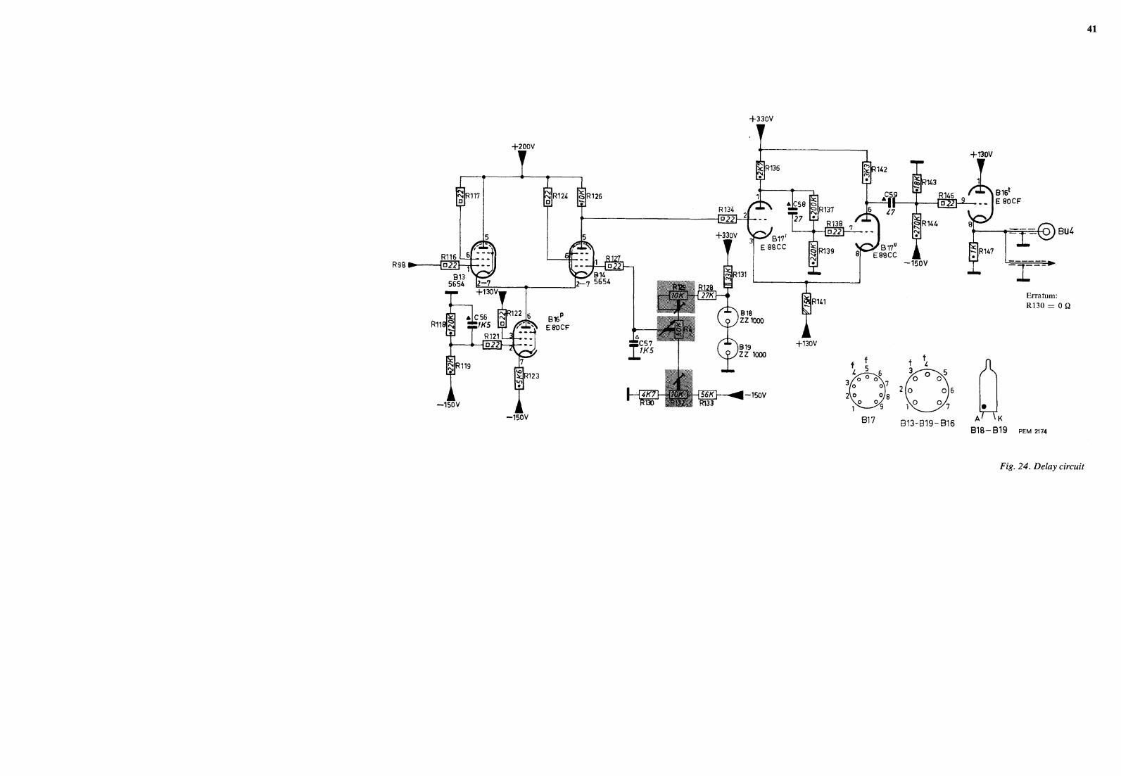
Erratum: R130 - 0 S2
B18 — 819 PEM 2174
Fig. 24. Delay circuit

45
I Ii
1 2
3 ~. 5
~~
O °
~--~~
6 O y ~ ~
8 0
9 0
10 C
11 0
12 0
13 0
14 O
15
1s o ..
17 ° 18
19 ~~'~ 20 21 O
.: 2 23
24 0
TC 47 A 1K8 F
~o I• II 6K8 ° —
o C 28 1~ o
o j~ 680 ° 11
i Qo ~I100K o i~ 56 0
~•,~ ~~ C31 ~t10K o
~~ a—~
0
0
A
o—
G °
c,----~
R80
F
(1M50
° RSG ~ C~ 750 ~—+ —a►
° R85 °---•—{300K~--~--D
°
C 32
~ ~ 3' 12
~ 3i x'12
0
0
° 1°o ~ a4 a
.o--~--~ 182:.. ® ~
C4G
o ' ~ 680 K o O °
!n1 Cris Lodo ~~ GB K. c
0 0
°T ~
U
976
—. R Bf — {14M8f
' R87
0
° ° n
0
°
Q ~ • R90
3M
~ t~ ~ /► R10G 187' 587" —)50V
Fig. 25. Time coef ficient switch
O
`J
0
0
PEM 3096 A
A

—~— 902/K •••
~% ~— 902/P•••
--{~— 900/P•••
o ~ 902/A•••
~~--904/••• 3
2
BU X 5 SK 3A
2~ }f Bt, 4, 6,11, 12,13, 14 ~" B~'~
t+12V 1 f 1 81, 4, 6, 11,12,13,14 r—`1
+400Y~---~
->-330 V ~-~-~
12 SK 7Aa 61 +1 30 V ~~y
SSK 7F ~
tOSK7F~
9I
10
11~
+G,3V ~ 12~
14~
35K6 15
16~
1~~9
81-B3-64-B6-811-612
~A
~B
GR1-GR4 GR6
~17 ►45K7F
~ff B3, 8,7
X18 iff 82,16
~✓♦R147,fiB16
~~ .+200V
~Z ►lSK7A
~iyy3 ► ff B17 (+70 V)
r4 ► 65K3F 125 ►ff B17
~6 ►11SK7F
IZZ /-R6
~- iff 82,161-70V)
I34 ~ -150V
i31 ►25K6 2
022
R100
A
K
GR2 GR3
f f 4
62- B7- BS
lA
~K
GR5-GR7 GR8-GR9
S SK1 A
0 1C3 ~
• 9 ~ /OK 1QUO
B9 k~a
248U X
R7
6 27 BU X~-~•33
BU1
1BUX~
R
L4
SK3F
8
S K3A 12
10
~6K
R9
6.75 V f
OV
_ SK 2
O
TV. SV11C} SEPARA70R !,a: .
GR 5 AAZ 17 B
11
SK1I A
ASZ20 R12
Cb
tom'--'
1.4V 5+4~r--~---~-_-
;; +6.25 V
\O6
3
-6,3 V
T5 2
ASZ2o
+6,3V
+6,2V --- --{-
11V
it
60. C1i56K e3
R37 F~ R39
+170V
R41
T53
ASZ20
10
SK1- A
4.8 V _i
i 211K5
~ 1Mr' R40
11 II
i SK1 F
~5 5 i
/ SK1 F
1
0.5 V ~ ~
~ -100mV
17
~ C9 • 3K9
C9•~ 3K9T•
GR6 C11LL • r
OA85 3K9
~C10 •T 3K9
4.25 V OV
R43
C22
11K5
TRIGGER AMPL.
t 130V
-1•E88CC 3
R36
--'SOV
+100 V
1± V
+190 V
R44 --- ~~00
E81~ 88CC ~R45
I L_
\T
_f4.8 V
+ 200 Y
R5
83' EBBC
SCHMIDT TRIGGER
-150V
f7K14 GR3
OA2~2 GR2= C16~ ~,R22
OA 202 G7K •-
• •
+200V
C 23 27 R63
~022~- ~j ---
R61
RGS
+13ov
a SK1 A
_~8p 3
3 r -O
R23
-ISOV
3
R2
-150V
+125V
60 V
R78
+200 V
7,2V ~ ~~
B 3' E 88 CC
1
R708 ~~ ___ 812
10 022 2 E88CC
C 52 ~~.~~ 3 T 1K5 3
I
R66
R27
R 28
-150V
GR4
-150V+130 V
C25
+200V
R68 ~~ ~o R69 ~ EBBC R71
6t ~~022
C 24 R67 ~~ 84"
f o22 ~ - EBBCC
100 ~ i ~~
8
h
+130V
1
R79
• R72 ~ 5.6~C26
T R 76
17 SZ R70
R73 a
-150V
X76
612"j ~\ ~ R 10 6
EBBCp - 91T~~
II
r -37 V ~ ~
17BUX 9BUX 228UX 6BUX
GR9 AAZ I S
B 4' E 88CC~~
-i50V
SWEEP GATING
MULTIVIB
~1 j
-57.SV
R 107
- 150V
1
B2t / E80CF - -
N OA70
B2RE$OCF
R31 g {o22h
R 29
-150V
AUTOMATIC STAB. CONTR:
R32
R 33
R34
-150V
HOLD. OFF. CIRCUIT
B 11' E88CC -
~C51
CI.p,C41
SK42F -i50V
42.5 V
42.5 V
R 82
I i
ep
i 11 I
1 I G R10 BAY38
N tz •6
SK7A
—2.4 V
0+ V
,~
SK4TA SK F I+130V+400Y
. • ~
87~ 5726
83 B7" . 1
C TB=C28,29,31, C 32,34,
N ~ R701
i 2
_L~TB I I I i
RB9
E80CF
~ TB=R80,84,85, ~~ R86,87,90
1
-150V
a 3 90K
26BUX WBUX
I I 11
R1G I I
/
n O
--41 10 SK7F
~ 36 1K R~3
8 9 ,~ A 1006
Y
-lsov MILLER TB CIRCUIT
+2o0V
R94 R96
R 98
R99
-150V
+130V
R110
R113
R115
B 8fEBpCF
R 97
-150V
318U X
-150 V
~`n
,
I ~
I~
6
_ B11~~ EBBC
e.y
0 R116
110V
-SV
DELAY CIRCUIT
f Qo BU3 --~~—~
-150V
--O
158U X
O
PEM 2173 A
Fig. 26. Time-base generator circuit
49