Performance Characteristics of IC Packages 4 · example, a pin inductance is a partial-self...
66
2000 Packaging Databook 4-1 Performance Characteristics of IC Packages 4 4.1 IC Package Electrical Characteristics As microprocessor speeds have increased and power supply voltages have decreased, the function of the microprocessor package has transitioned from that of a mechanical interconnect which provides protection for the die from the outside environment to that of an electrical interconnect that affects microprocessor performance and which must be properly understood in an electrical context. Inherent in understanding the electrical performance effects of the package is the need for electrical characterization of the package. The package is a complex electrical environment and the characterization of this environment is a multi-faceted task that consists of models constructed from both theoretical calculations and experimental measurements. In simple terms, a package electrical model translates the physical properties of a package into electrical characteristics that are usually combined into a circuit representation. The typical electrical circuit characteristics that are reported are DC resistance (R), inductance (L), capacitance (C), and characteristic impedance (Z_o) of various structures in the package. A package model consists of two parts, both of which are necessary for fully understanding the electrical performance effects of the package environment on Intel’s microprocessors. The first is an I/O lead model that describes the signal path from the die to the board. Depending upon the complexity of the model required for simulation purposes, the I/O lead model can take the form of a simple lumped circuit model, a distributed lumped circuit model, a single-conductor transmission-line model, or a multiple-conductor transmission-line model. While lumped models can adequately model simple effects, such as DC resistive voltage drop, more sophisticated models like the multiple-conductor transmission-line model include effects such as time delay and crosstalk. The second part of a package model is a power-distribution network that describes the power scheme of the package. Like the I/O lead model, the sophistication of the power-distribution network can vary from a simple distributed lumped model to a complex circuit network called a PEEC (partial-element equivalent circuit) network. The simpler models can describe gross electrical characteristics of the power-distribution network, such as DC resistive drop for the entire package, whereas the more complex models enable the analysis of the effects of the power- distribution topology. Experimental characterization of the package can include measurements of trace characteristics and power loop parasitics, to name a few of the package aspects that can be characterized. Experimental characterization is usually the final, validation stage of the package-design process. Care must be taken in determining the characteristics that are measured. If a comparison between measured and modeled data is to be made, then the same assumptions used in obtaining the theoretical package model must be replicated in the test environment. The following sections provide an overview of basic package modeling terminology and methodology, an overview of experimental characterization, and modeled data for the packages that Intel uses for its most advanced microprocessors. These products are housed in packages representative of a broad spectrum of package technologies, including CPGA (ceramic pin-grid array), PPGA (plastic pin-grid array), H-PBGA (high thermal plastic ball grid array), TCP (tape carrier package), OLGA (organic land-grid array), and FC-PGA (flip-chip pin-grid array). For the
Transcript of Performance Characteristics of IC Packages 4 · example, a pin inductance is a partial-self...

ding ke the r els
models
r
a
ntire
stics cess. tween e
ges es rid e the
Performance Characteristics of IC Packages 4
4.1 IC Package Electrical Characteristics
As microprocessor speeds have increased and power supply voltages have decreased, the function of the microprocessor package has transitioned from that of a mechanical interconnect which provides protection for the die from the outside environment to that of an electrical interconnect that affects microprocessor performance and which must be properly understood in an electrical context. Inherent in understanding the electrical performance effects of the package is the need for electrical characterization of the package. The package is a complex electrical environment and the characterization of this environment is a multi-faceted task that consists of models constructed from both theoretical calculations and experimental measurements.
In simple terms, a package electrical model translates the physical properties of a package into electrical characteristics that are usually combined into a circuit representation. The typical electrical circuit characteristics that are reported are DC resistance (R), inductance (L), capacitance (C), and characteristic impedance (Z_o) of various structures in the package. A package model consists of two parts, both of which are necessary for fully understanding the electrical performance effects of the package environment on Intel’s microprocessors.
The first is an I/O lead model that describes the signal path from the die to the board. Depenupon the complexity of the model required for simulation purposes, the I/O lead model can taform of a simple lumped circuit model, a distributed lumped circuit model, a single-conductotransmission-line model, or a multiple-conductor transmission-line model. While lumped modcan adequately model simple effects, such as DC resistive voltage drop, more sophisticated like the multiple-conductor transmission-line model include effects such as time delay and crosstalk.
The second part of a package model is a power-distribution network that describes the powescheme of the package. Like the I/O lead model, the sophistication of the power-distribution network can vary from a simple distributed lumped model to a complex circuit network calledPEEC (partial-element equivalent circuit) network. The simpler models can describe gross electrical characteristics of the power-distribution network, such as DC resistive drop for the epackage, whereas the more complex models enable the analysis of the effects of the power-distribution topology.
Experimental characterization of the package can include measurements of trace characteriand power loop parasitics, to name a few of the package aspects that can be characterized.Experimental characterization is usually the final, validation stage of the package-design proCare must be taken in determining the characteristics that are measured. If a comparison bemeasured and modeled data is to be made, then the same assumptions used in obtaining ththeoretical package model must be replicated in the test environment.
The following sections provide an overview of basic package modeling terminology and methodology, an overview of experimental characterization, and modeled data for the packathat Intel uses for its most advanced microprocessors. These products are housed in packagrepresentative of a broad spectrum of package technologies, including CPGA (ceramic pin-garray), PPGA (plastic pin-grid array), H-PBGA (high thermal plastic ball grid array), TCP (tapcarrier package), OLGA (organic land-grid array), and FC-PGA (flip-chip pin-grid array). For
2000 Packaging Databook 4-1

Performance Characteristics of IC Packages
r Intel’s
the
f DC ed by C
ten f
ng onstant t of
e nce of
ually be e. The
sake of completeness, package parasitics data for older package technologies are included in the final part of this section. The package types included are multilayer molded (MM-PQFP), ceramic quad flatpack (CQFP), plastic leaded chip carrier (PLCC), quad flatpack (QFP, SQFP, TQFP), and small outline packages (TSOP, PSOP). These packaging technologies are no longer used foleading-edge microprocessors but are still used for other products.
Since the packages used for Intel’s microprocessors are custom designed for each product,parameters given in the following sections may not reflect the actual values for a particular product. The actual parameters can be obtained by contacting a local Intel sales office. For electrical parameters of packages not listed, please contact your local Intel field sales office.
4.1.1 Terminology
4.1.1.1 DC Resistance (R)
The DC resistance (R) is normally the cause of IR voltage drops in the package. Reduction oresistance is particularly important in the power and ground paths. DC resistance is determinthe cross-sectional dimensions (width and thickness), material, and length of the lead. The Dresistance of an I/O lead with cross-sectional area, A, length, L, and resistivity, ρ, can be calculated using:
Equation 4-1.
Ceramic packages have relatively high resistance because of the high resistivity of the tungsalloy metallization used with ceramic technology. Plastic/organic packages have much lowerresistance because the metallization used is either copper or a copper alloy. The resistivity ocopper or copper alloys is approximately a factor of 6-12 lower than that of tungsten alloys.
4.1.1.2 Capacitance (C)
Capacitance (C) is determined by the lead length and cross-sectional dimensions, the spacibetween leads, the spacing between the lead and the power or ground plane, the dielectric cof the surrounding material, and the number of leads involved. The relative dielectric constanthe material used for ceramic packages is in the range of 8–10. The dielectric constant of thmaterial used for plastic packages is in the range of 4–6. There are formulas for the capacitaclassic geometries; however, the capacitance for a particular structure in a package must uscalculated using a software modeling tool. The formula for the capacitance of a parallel platecapacitor can be used to deduce the general relationship between geometry and capacitanccapacitance for this structure, neglecting fringing fields, is:
Equation 4-2.
where A is the area of one of the plates, ε is the permitivity of the material separating the plates,and t is the thickness of the material.
RρLA
------=
Cε At
------=
4-2 2000 Packaging Databook

Performance Characteristics of IC Packages
ce, tal e is the s in the gonal
tance , the ll as is es as a C .
cross ackage oise. ever,
o each For
s at
avior p
l to can nce of
e the entire hen ed, and e is w
and a y ly for
Capacitances which are important to package electrical performance are “loading” capacitan“lead-to-lead” capacitance, and “decoupling” capacitance. The loading capacitance is the tocapacitance of a lead with respect to all surrounding conductors. The lead-to-lead capacitancmutual capacitance between the two leads. The loading capacitances are the diagonal termso-called “short-circuit” capacitance matrix, and the lead-to-lead capacitances are the off-diaterms. The lead-to-lead capacitance and the mutual inductance determine the extent of electromagnetic coupling between the two leads. Decoupling capacitance is the total capacibetween the power leads and the ground leads. In a ceramic PGA with power/ground planesdecoupling capacitance is due to the capacitance between power and ground planes, as weadded discrete capacitors to the package. In plastic PGA packages, decoupling capacitanceusually provided by adding discrete capacitors to the package. Decoupling capacitance servreservoir which provides part of the energy required when buffers switch. This reduces the Avoltage drop, also called the switching noise or the ground bounce, of the power/ground path
4.1.1.3 Inductance
A simple definition of inductance (L) is the property of a conductor that describes the proportionality between current change and induced voltage. An inductor is any conductor awhich there is a voltage drop when there is a time-varying current present. This aspect of a pis important in determining the extent of the effects of crosstalk and simultaneous switching nThe classical definition of inductance implies that the inductance is that of a current loop, howa loop can be segmented, and partial-self and partial-mutual inductances can be attributed tsegment. This is a useful concept for analyzing package AC noise and is widely used today.example, a pin inductance is a partial-self inductance.
Another useful term is the “open-loop” inductance which is the inductance of a loop with gaptwo ends. We can visualize a segment of a transmission line as an open-loop and the total inductance of that segment as the open-loop inductance. Inductances used in analyzing behsuch as propagation delay and crosstalk of electrical interconnects are, in general, open-looinductances.
When partial inductances are used in package electrical performance analysis, it is essentiaunderstand the current direction in each segment. Wrong assumptions on current directions lead to erroneous results. The term “current return path” is widely used to stress the importaunderstanding the current direction in each segment involved.
The inductance values are determined by the lead length and cross-sectional dimensions, thspacing between leads, the spacing between the power or ground plane, the permeability ofconductor, and the number of leads involved. A general rule of thumb is that the smaller the current loop involved the lower the inductance. This is an important concept to be aware of wdesigning packages and systems, in general. Each signal needs to have a nearby, well-defincontinuous return path. There are few simple formulas for inductance because the inductancdependent upon both the physical geometry of the structure and the current return path. A feclassic problems have been solved in closed form. Software codes that use electromagneticanalysis techniques are usually used to compute the inductance of the complex structures inpackages.
4.1.1.4 Characteristic Impedance (Z_o)
Characteristic impedance (Z_o) is one parameter that is used to describe transmission-line structures, which are any structures consisting of two conductors - a signal conductor (lead) reference conductor, typically a power/ground plane. In package modeling, traces are usualldescribed in terms of transmission-line parameters because this type of description inherentincorporates time delay. A model that consists of lumped circuit components cannot accountthe time delay of the signal through the package.
2000 Packaging Databook 4-3

Performance Characteristics of IC Packages
rds pt to 2-ohm
river s age is arily onger o, the lanes
nce st be ds to
als. n the
sually und he
s the dget ugh to verall insure er
The characteristic impedance of a line can be found using:
Equation 4-3.
L and C are per-unit-length values of the inductance and capacitance of the line, so Z_o is independent of line length.
Z_o is an important factor in determining the amount of signal reflection that will occur at the boundary between the die and the package and at the boundary between the package and the board. The amount of reflection and, thus signal distortion, is directly proportional to the amount of mismatch between Z_o’s at these boundaries. As an example, the Z_o of traces in FR-4 boatypically used for motherboards is around 50 ohms, so typical packaging technologies attemmatch this impedance as closely as possible. For example, a typical CPGA package has a 4trace impedance and a typical PPGA package has a 47-ohm impedance.
4.1.1.5 Crosstalk
Crosstalk refers to unwanted signal coupling between lines. It is a complex function of the dand receiver characteristics, trace characteristics, and switching patterns. Some generalitieregarding package design and its relationship to crosstalk can be made. Crosstalk in a packdependent upon the stack-up, just as is characteristic impedance; however, crosstalk is primaffected by the distance between traces and the amount of parallelism between them. The lthe parallel distance between two or more lines, the higher the crosstalk between them. Alscloser the lines are to one another, the higher the crosstalk. The proximity of power/ground pto the traces can help reduce crosstalk. That is, crosstalk is directly proportional to the distabetween the planes above and below the trace. There are no simple formulas for predictingcrosstalk. Models of the traces, with the mutual inductance and capacitance calculated, mugenerated and simulations run using buffer models and models representing the system loacorrectly determine the amount of crosstalk in a package design or system.
4.1.1.6 Simultaneous Switching
A final concern in package and system design is the effect of simultaneous switching of signThere are two items of concern when many signals switch simultenously: noise generated opower/ground planes and timing pushout of signals. The first item, power/ground noise, is ureferred to as "SSN", simultaneous switching noise, and is the noise generated in power/grostructures due to a changing current and inductive elements in the power delivery system. Tsecond item is usually referred to as "SSO (simultaneous switching output) pushout." This idifference in timing between single-bit and multiple-bit switching. System designers must bufor the worst-case switching case upfront in their design to insure a design that is robust enohandle all switching cases. Analyses of SSN and SSO are very complex but critical to the odesign process. The general guideline to mitigate the impact of simultaneous switching is to that all signals have well-defined return paths with low inductance and to insure that the powdelivery network has a low inductance. Models and simulations for simultaneous switching phenomenon are very complex and product dependent and, thus, will not be included in thisdocument. Please contact your Intel field sales office for product-specific models.
Z_o LC----=
4-4 2000 Packaging Databook

Performance Characteristics of IC Packages
4.1.2 Modeling Methodology
The exact format for a package model depends upon the model usage. For analyzing specific critical signals, it is necessary to model only a few I/O signal leads in a small section of the package. For designing a power supply scheme, it is necessary to model the power supply loop for the entire package. A complete package model consists of an I/O signal lead for a typical lead geometry plus power loop models for each isolated power supply in the package. The amount of detail included in the model and the exact format of the model are items that the packaging engineer must determine based upon assessments of the model usage and the system characteristics. The next few sections outline some of the issues that the packaging engineer must consider in creating an appropriate package electrical model.
4.1.2.1 I/O Signal Lead Model
The I/O signal lead model consists of the parasitics for a particular signal path in the package. For a wirebond, pin-grid array (PGA) package, the signal path includes the bondwire, the trace, vias, the pin, and the plating bar. Intel has migrated to flip-chip packaging (OLGA and FC-PGA) for its higher performance products. For these types of packages, the signal path includes the solder bump connection between the die and package, the trace, vias, and the pins or lands. If crosstalk is to be considered, then the cross-coupling parasitics for the nearest leads should also be included in the model. Ordinarily it is useful to analyze the lead both in isolation and in conjunction with the nearest traces on either side of the lead.
The key to providing an accurate I/O signal lead model is to identify the return current paths. For example, in analyzing the I/O signal lead bondwire inductance, the closest current return path is the nearest power or ground bondwire. If the effect of this bondwire is not included in the analysis, then the calculated I/O signal lead bondwire inductance will be higher than it actually is because the mutual effects of nearby wires have not been included. In analyzing the signal trace, it is necessary to identify the nearest current-carrying package planes that provide a current return path. In effect, signal traces are usually modeled as microstripline or stripline structures, where a microstripline structure is defined as a trace with one current-carrying plane in close proximity and a stripline structure is defined as a trace sandwiched between two current-carrying planes.
Unless a highly accurate model for a particular critical signal is required, the I/O signal lead model for a package is usually based upon the typical lead geometry. Crosstalk parameters are usually based upon the worst-case crosstalk scenario, i.e., the minimum trace spacing. Typically, the individual components comprising the signal lead are modeled individually using two and three dimensional solutions obtained using electromagnetic field-solving software. The primary parasitics of interest are the line characteristic impedance (Z_o), the line inductance (L), the line resistance (R), the line capacitance (C), and cross-coupling L and C matrices for crosstalk analysis. SSO models usually include mutual effects between signal lines and include the power distribution network effects. To obtain the level of accuracy and complexity required for SSO modeling, three-dimensional fully coupled models are necessary.
4.1.2.2 Power Loop Models
The power loop model consists of the structures used for power delivery in the package. Typically, all power and ground bondwires, vias, planes, and pins must be included along with mutual effects between structures in close proximity to one another. The format for the power loop model is not as straightforward as for the I/O signal lead model because of the complexity of the system. To accurately model the power loop, the entire package structure must be comprehended. This is an unwieldy task, so the packaging engineer must use approximations and partitioning of the package structure to simplify the model. The amount of complexity that is included depends upon the usage. A simple distributed lumped model may be sufficient for certain analyses; however, a more
2000 Packaging Databook 4-5
Performance Characteristics of IC Packages
complex model is usually required for making power distribution design decisions, such as determining the quantity and location of power and ground pins and bondwires and the quantity and location of decoupling capacitors.
A simple distributed model usually consists of a single resistor/inductor element to represent each major structure in the package. For example, all the power bondwires are considered to be parallel, equivalent resistive/inductive structures, so their parasitics are lumped into one resistor/inductor element. Similarly, all the pins and vias are lumped together, and each plane is represented as a single resistor and inductor. This is a highly simplistic model which assumes equal current flow through each pin. Although this is not a very accurate model, it is quite useful for obtaining an approximation for the total package resistance and inductance. To more accurately model the intricacies of the power distribution in the package, all elements must be represented by circuits that contain both self and mutual inductance and capacitance terms. This type of representation is typically called a PEEC (partial-element equivalent circuit) network and must be generated using software tools that solve electromagnetic field equations. The drawback of this type of model is that it consists of a large, complex circuit with many individual elements. The effects of various elements are not intuitively obvious, so circuit simulations must be run. Since the network is large, much computer memory and simulation time is required for this type of analysis.
4.1.2.3 Trade-Offs Between Accuracy and Complexity
Package modeling is both a science and an art. Ideally, one would like to be able to exactly and entirely model the package; however, this is extremely impractical, if not impossible. Both the amount of computational resources and the complexity of the final package model are prohibitive. On the other hand, using a very convenient approach of modeling the entire package as an R, L, C circuit whose parameter values are determined from closed form formulas is crudely simplistic. Somewhere between these extremes lies the realm in which the packaging engineer realistically must develop electrical models for the package.
Inherent in this development is the decision of how much loss in accuracy is acceptable in order to provide a convenient and usable model. This is a decision that is best made after experimentation to test for convergence of a model and, ideally, after comparison to measured data. In general, a single I/O lead model can be quite accurately constructed using two-dimensional approximations for the trace itself and even for the bondwire. Three-dimensional modeling is usually required for the pin and via. All these structures can be easily created and accurately analyzed using commercial software tools for solving electromagnetic field equations. Because of its complexity, there are more engineering approximations that must be made in constructing a model for the power supply loop. For example, a power plane may have a hundred vias connected to it; however, inputting this complex geometry into a software tool would be a time-consuming task. In addition, analyzing this type of geometry would require large quantities of computer memory and time. The accuracy lost in grouping vias together may be very small, i.e., one via could be used to represent ten vias in close proximity. After some practice and experimentation, one can learn to recognize opportunities for model simplification which will not overly compromise accuracy.
4.1.2.4 Lumped-Element Models versus Transmission-Line Models
One key choice that must be made in creating a package model is whether to represent package structures as lumped circuit elements or as transmission-line elements. The general guideline that is given throughout packaging literature is that a transmission-line model should be used if:
4-6 2000 Packaging Databook

Performance Characteristics of IC Packages
d a
ture is
be
uted urface o an uency- of the tional
use nal
l ing
e lculated e
is in h is e. For , there
Equation 4-4.
where is the round-trip delay in the medium in which the signal path lies and is the risetime of the signal. As an example, a typical package trace in a ceramic package is around 1 inch long. Using a dielectric constant of 10 for ceramic, the round-trip delay is:
Equation 4-5.
This is the order of the risetimes for signals in today’s microprocessors. Therefore, using a transmission-line model for traces in a package is an appropriate modeling decision.
Typically, a transmission-line model should be used for the trace and lumped models for the bondwires, pins, and vias. Most of the time delay in the package is due to the trace delay, antransmission-line model for the trace will appropriately account for the time delay. A lumped model cannot account for time delay and should only be used when the delay through a strucnot a significant portion of the overall signal propagation delay. As risetimes decrease and propagation delays through the package become more critical, transmission-line models willnecessary for many structures in the package.
4.1.2.5 Frequency-Dependent Effects
Another choice that must be made in creating a package model is whether or not to include frequency-dependent effects. To briefly summarize the issue, at DC, current is evenly distribacross the cross-section of a conductor. At high-frequencies, the current is confined to the sof the conductor. At frequencies in between DC and high-frequency, the current is confined tarea defined as the skin depth of the conductor. Skin depth is material-, geometry-, and freqdependent and decreases with increasing frequency. Because of the frequency dependenceskin depth, the resistance and inductance of a conductor vary with frequency. The cross-secarea through which current flows in a conductor is also affected by the presence of other conductors. This phenomenon is called the proximity effect.
It is usually adequate to simply model the DC resistance of a conductor in a package and tohigh-frequency, or quasi-static inductance calculations to model the inductance. Because sigrisetimes are decreasing with each new generation of microprocessor, however, the spectracontent of typical signal waveforms is increasing and frequency-dependent effects are becommore critical to accurate package analysis. For this reason, future package models should includboth frequency-dependent resistance and inductance values. These parameters must be causing software tools which accurately perform a full-wave solution to Maxwell’s equations, thequations which describe electromagnetic field interactions.
4.1.2.6 Power-Distribution Design Concepts
There are many applications for a complete and accurate package model. The obvious use analyzing signal distortion and delay through the package environment. A second area whicvery important, but not as obvious, is in designing the power decoupling scheme for a packagpower-distribution design, there are a few general guidelines that should be mentioned. First
tr 2tol<
2tol tr
2tol 2 εrεo µo× l× 2εrc
---------× l 2= 10
3 1010
cm/s×---------------------------------×× 2.54 cm/in. 1 in.×× 0.54 ns= = =
2000 Packaging Databook 4-7

Performance Characteristics of IC Packages
he
e an ires e user l ique eful or ries that ing
ories. s y
the the
are two types of decoupling: low and high-frequency. Low-frequency decoupling is used on the board to typically control the noise from the power supply entering the board. High-frequency decoupling is used on the package and chip to control simultaneous switching noise.
When decoupling capacitors are placed on the package, they should be placed as close as possible to the die to minimize stray inductance associated with the connection between the capacitor and the die. It is important in using any type of decoupling capacitor to try to minimize the stray resistance and inductance associated with the interconnect and the capacitor itself. This is more important for high-frequency decoupling than low-frequency. In general, low-frequency decoupling schemes require large values of capacitance. Larger inductances are usually associated with larger capacitors. High-frequency capacitance values should be small to reduce the associated stray inductance.
The placement of decoupling capacitors affects the overall effective inductance; therefore, a fairly complex package model that allows analysis of the effects of capacitor placement is usually necessary for power-distribution design. The package model for this use, therefore, should take the form of a complex distributed model, or partial-element equivalent circuit (PEEC) model.
4.1.2.7 Modeling Tools
The theoretical values for package parameters are obtained at Intel by using in-house and commercial two-dimensional and three-dimensional modeling tools. The software calculates the inductance, capacitance, resistance, and characteristic impedance values based upon physical design parameters, such as geometry information and material properties, which are input using a CAD-based graphical interface. The user can usually input this information manually or use interface modules which can convert physical design databases for the package geometry into the appropriate format for the modeling tool.
Most of these tools are based upon numerical solutions of electromagnetic field equations, i.e., Maxwell’s equations. The techniques used vary according to the software vendor. Some of tmost common solution techniques include moment method, finite-element method, finite-difference time-domain technique, and boundary-element method. Although one need not bexpert, using commercially available software tools which use these techniques usually requthat one be somewhat knowledgeable about the basic theory behind the technique becauseadditional user input is usually required to accurately solve for the parasitics. For example, this usually required to specify the meshing scheme used to divide the geometry for numericaanalysis. One should also be aware of the limitations and requirements of the tool and technused for solving for package parasitics or one could inadvertently produce data that is not usaccurate. Some of the issues that should be understood are the limits on the types of geometcan be analyzed, the assumptions concerning return-current paths, the assumptions concernground planes and ground conductors, and the underlying analysis algorithms.
4.1.3 Experimental Characterization Methodology
4.1.3.1 Equipment
The equipment necessary for characterizing the parasitics of a package falls into three categThe first is measurement equipment, which is standard and available from several companiewhich specialize in the design and manufacture of this equipment. A well equipped laboratorshould contain a D.C.-ohmmeter, an impedance analyzer, a network analyzer for frequency-domain characterization, and a time-domain reflectometry (TDR) set-up for time-domain characterization. The second category is test fixtures. These must be specially designed forpackage and structure being characterized. Methods for de-embedding the test fixture from
4-8 2000 Packaging Databook

Performance Characteristics of IC Packages
measurement must be devised. The third category is probes. Most package measurements involve probing very small structures with fixed pitches. Probes and calibration standards for these probes are available from companies which specialize in this area.
The following sections outline some of the basics for measuring I/O signal lead and power loop parasitics. It is impossible to cover the intricacies of measurement technique adequately in such a small space. Measurement methodology is continually evolving, and packaging engineers should remain in close contact with measurement equipment representatives and should keep up with conference proceedings and technical journals so that they are well informed concerning the latest and most accurate techniques. Regardless of the measurement technique, the packaging engineer should take care to model and measure the same scenarios if reliable validation data is to be obtained.
4.1.3.2 I/O Signal Lead Characterization
4.1.3.2.1 DC Resistance
The resistance for a given CPGA package is measured from the tip of the bond finger to the pin braze pad. The lead resistance for plastic packages is measured from tip to tip. Figure 4-1 shows the four-probe setup used to measure resistance values. Two sets of readings are taken by reversing the direction of current to eliminate the contact potential. The average value is considered the resistance of the sample.
Figure 4-1. Four-Probe Set-up
4.1.3.2.2 Capacitance
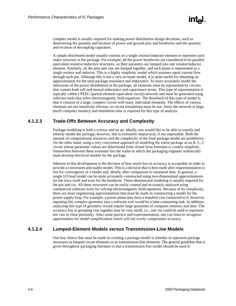
Loading capacitances are measured using an impedance analyzer. The setup for measuring loading capacitance is shown symbolically in Figure 4-2. In this setup, all leads except the lead of interest are grounded. The capacitance is measured between this lead and ground. Decoupling capacitance is measured between a power lead and a ground lead.
Voltmeter
Contact Potential
AmmeterPower SupplyWith Switch
δR
A5609-01240819-1
2000 Packaging Databook 4-9
Performance Characteristics of IC Packages
Figure 4-2. Set-up for Measuring Loading Capacitance
4.1.3.2.3 Inductance
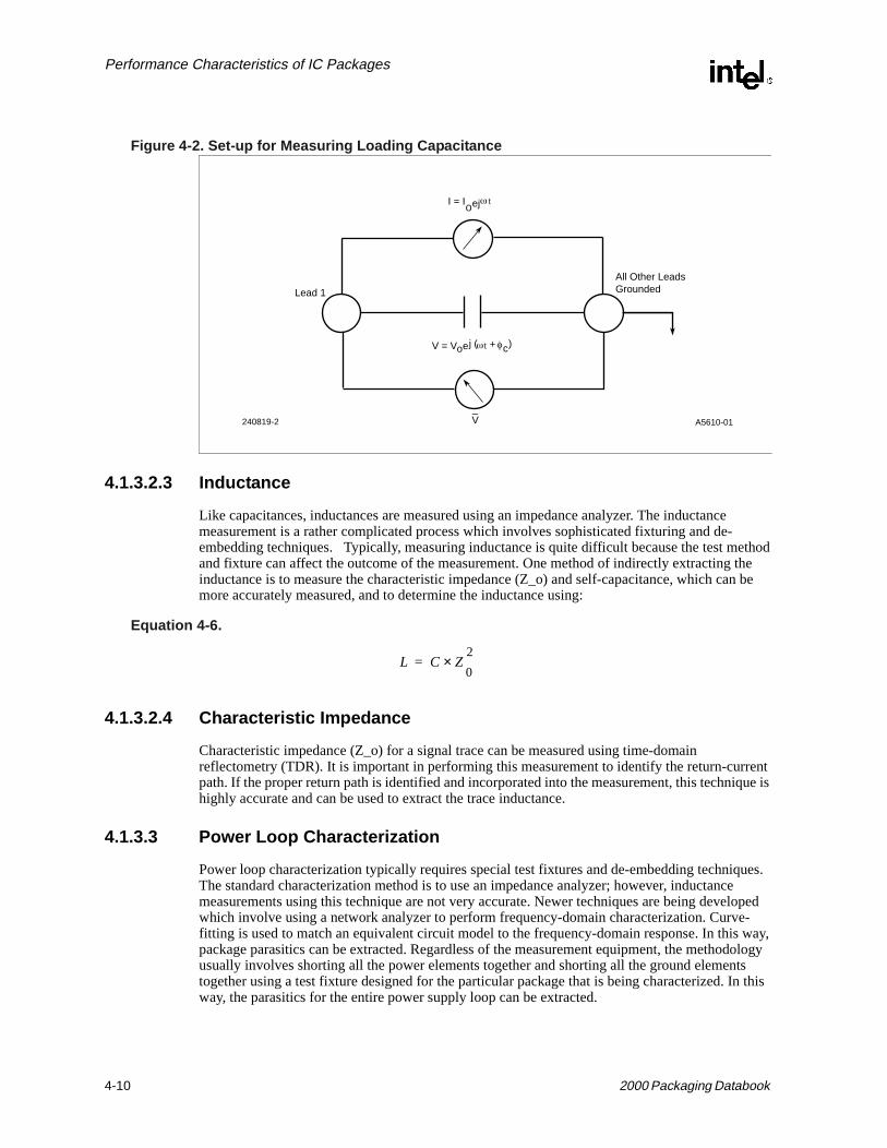
Like capacitances, inductances are measured using an impedance analyzer. The inductance measurement is a rather complicated process which involves sophisticated fixturing and de-embedding techniques. Typically, measuring inductance is quite difficult because the test method and fixture can affect the outcome of the measurement. One method of indirectly extracting the inductance is to measure the characteristic impedance (Z_o) and self-capacitance, which can be more accurately measured, and to determine the inductance using:
Equation 4-6.
4.1.3.2.4 Characteristic Impedance
Characteristic impedance (Z_o) for a signal trace can be measured using time-domain reflectometry (TDR). It is important in performing this measurement to identify the return-current path. If the proper return path is identified and incorporated into the measurement, this technique is highly accurate and can be used to extract the trace inductance.
4.1.3.3 Power Loop Characterization
Power loop characterization typically requires special test fixtures and de-embedding techniques. The standard characterization method is to use an impedance analyzer; however, inductance measurements using this technique are not very accurate. Newer techniques are being developed which involve using a network analyzer to perform frequency-domain characterization. Curve-fitting is used to match an equivalent circuit model to the frequency-domain response. In this way, package parasitics can be extracted. Regardless of the measurement equipment, the methodology usually involves shorting all the power elements together and shorting all the ground elements together using a test fixture designed for the particular package that is being characterized. In this way, the parasitics for the entire power supply loop can be extracted.
All Other LeadsGroundedLead 1
V_
I = I ej
A5610-01240819-2
t
V = V ej ( c)o +t
o
L C Z2
0×=
4-10 2000 Packaging Databook

Performance Characteristics of IC Packages
t A,
based he and as given. talk st. All
al mple, ire
r local
for the deled ion lines
the , ted on as he he s for
4.1.4 Product Package Models for Intel’s Leading-Edge Microprocessors
The following sections contain data describing the parasitics for the packages for Intel’s mosrecent microprocessors. The I/O signal lead, power loop, and crosstalk models for TCP, CPGPPGA, H-PBGA, OLGA, and FC-PGA packages are given. All values are calculated values upon the final package design and calculated using commercially available software tools. Tvalues given for the I/O signal lead models are given as ranges of values for the bondwires per-unit-length parasitics for the traces. The ranges for trace lengths in the package are alsoThe power loop model is based upon the typical package and microprocessor design. Crossmodels account for coupling between the closest signals on either side of the signal of interetransmission-line models and inductance values are calculated assuming high-frequency conditions, i.e., assuming that current flows on the exterior of the conductor only. Resistancevalues are calculated at DC. Transmission line models are used where necessary, and mutueffects of nearby current-return paths are incorporated into the final parasitic values. For exathe inductance of a bondwire is calculated by considering the particular location of the bondwwith respect to current-return paths. The inductance is not calculated assuming an isolated bondwire. For assistance in constructing models for specific leads in a package, contact youIntel field sales office for information pertaining to the lead of interest.
4.1.4.1 I/O Signal Lead Models
A single I/O lead in a package is modeled as a circuit consisting of representative elements bondwire, the trace, the pin or land, and the plating trace. Bondwires, pins, and lands are moas series resistors and inductors. The signal and plating traces are represented by transmisswith per-unit-length resistance (R), inductance (L), and capacitance (C) or with characteristicimpedance (Z_0). Figure 4-3 illustrates the generic I/O lead model for any multilayer package technology. This circuit can be used to describe a specific package technology by changing parasitic values to match the technology. Table 4-1 lists the typical parasitics for the CPGA, PPGAH-PBGA, OLGA, and FC-PGA packages. The values listed assume that the package is mounthe motherboard using a socket, so the pin/land parasitics include the socket effects as well connecting via parasitics inside the package. For flip-chip packages (OLGA and FC-PGA), tbondwire is replaced by the die bump and connecting via and there are no plating traces. Tvalues given in this section are for typical cases only. For more accurate data for simulationspecific signals on specific products of interest, contact your local Intel field sales office.
2000 Packaging Databook 4-11

Performance Characteristics of IC Packages
Figure 4-3. Package I/O Signal Lead Model for Multilayer Packages
Because the geometry of TCP packages is very different from that of multilayer packages, another circuit representation for the package model must be used. This is shown in Figure 4-4. The model consists of three transmission lines with different parasitics that represent different portions of the signal path through the package. Typical TCP parasitics are given in Table 4-2.
Table 4-1. Summary of Package I/O Lead Electrical Parasitics for Multilayer Packages
Electrical ParameterWirebond Package Type Flip-chip Package Type
CPGA PPGA H-PBGA OLGA FC-PGA
Bondwire/Die bump R (mohms) 126 - 165 136 - 188 114 - 158 2 0.06
Bondwire/Die bumpL (nH) 2.3 - 4.1 2.5 - 4.6 2.1 - 4.1 0.02 0.013
Trace R (mohms/cm) 1200 66 66 590 120
Trace L (nH/cm) 4.32 3.42 3.42 3.07 2.329
Trace C (pF/cm) 2.47 1.53 1.53 1.66 1.707
Trace Z_0 (ohms) 42 47 47 43 38.5
Pin/Land R (mohms) 20 20 0 8 20
Pin/Land L (nH) 4.5 4.5 4.0 0.75 2.9
Plating Trace R (mohms/cm) 1200 66 66 N/A N/A
Plating Trace L (nH/cm) 4.32 3.42 3.42 N/A N/A
Plating Trace C (pF/cm) 2.47 1.53 1.53 N/A N/A
Plating Trace Z_0 (ohms) 42 47 47 N/A N/A
Trace Length Range (mm) 8.83 - 26.25 6.60 - 42.64 4.41 - 22.24 3.0 - 18.0 10.0 - 42.6
Plating Trace Length Range (mm) 1.91 - 10.50 1.91 - 16.46 0.930 - 8.03 N/A N/A
A5681-01
Board
Pin / Land
Pin / LandL Pin / LandR
Trace
Tiebar L, R, C
bwL bwR
BondwireccpV
Vssp
4-12 2000 Packaging Databook

Performance Characteristics of IC Packages
Figure 4-4. Package I/O Signal Lead Model for TCP Packages
4.1.4.2 Power Loop Models
There are many different methods of representing the power loop parasitics in a package model. As a general rule, the more distributed the model, the more accurate the model. As a comparative tool, however, this type of model is not very useful. To provide a simple model by which the overall power loop parasitics of different packaging technologies can be compared, the model shown in Figure 4-5 is used here. The overall inductance and resistance of the power loop for the core (Vcc and Vss) power supply have been calculated and are given in Table 4-3. As in the previous section, the parasitic values for the multilayer packages include the effects of a socket. This is a highly simplistic model but a good one for comparing the different packaging types. For more accurate data for simulations, contact your local Intel field sales office
Table 4-2. Summary of Package I/O Lead Electrical Parasitics for TCP Packages
Electrical Parameter
Trace Segment
Inner Lead Segment
Fan-Out Lead Segment
Outer Lead Segment
Trace Segment R (mohms/cm) 352 290 144
Trace Segment L (nH/cm) 6.48 - 8.84 6.43 - 8.81 7.56 - 9.77
Trace Segment C (pF/cm) 0.58 - 0.83 0.13 - 0.19 0.12 - 0.16
Trace Segment Z_0 (ohms) 89 - 124 183 - 256 220 - 288
Trace Segment Length Range (mm) 0.90 - 4.0 0.05 - 11.8 0.91 - 3.25
A5682-01
Board
ccpV
Vssp
Outer Lead TraceSegment
Fan-Out Lead TraceSegment
Inner Lead TraceSegment
L, R, C, Z_0 L, R, C, Z_0L, R, C, Z_0
2000 Packaging Databook 4-13

Performance Characteristics of IC Packages
only. l field
Figure 4-5. Package Core Power Loop Model
4.1.4.3 Cross Talk Models
As devices migrate to lower voltage designs and smaller packages, the detrimental effects of crosstalk become more pronounced. Care must be taken in package design to minimize and quantify crosstalk. To simulate the effects of crosstalk, an appropriate model is needed. The model included in this handbook, Figure 4-6, is for coupling between three parallel signal leads located at minimum spacing for the package technology from one another. Figure 4-6 illustrates the numbering convention and placement of the signal leads. Table 4-4 gives the inductive coupling coefficients, and Table 4-5 gives the capacitive coupling coefficients for the CPGA, PPGA, TCP, H-PBGA, OLGA, and FC-PGA packages. Note that the mutual terms have negative signs, which is the convention for the “short-circuit” matrix representation. These values are for typical casesFor more accurate data for simulations for specific signals of interest, contact your local Intesales office.
Table 4-3. Summary of Package Core Power Loop Electrical Characteristics
Electrical ParameterPackage Type
CPGA PPGA TCP H-PBGA OLGA FC-PGA
R_Vcc (mohms) 5.5 2.0 6.0 4.1 0.5 1.2
L_Vcc (pH) 150 150 150 217 15 64.4
R_Vss (mohms) 5.5 2.0 6.0 4.1 0.5 1.2
L_Vss (pH) 150 150 150 198 15 64.4
A5680-01
Die Board
R_Vcc
R_VssL_Vss
L_Vcc
4-14 2000 Packaging Databook

Performance Characteristics of IC Packages
y
ot ions
Figure 4-6. Package Crosstalk Model
4.1.4.4 SSO Models
Models and simulations for simultaneous switching phenomenon are very complex and product dependent and, thus, will not be included in this document. Please contact your Intel field sales office for product-specific models.
4.1.5 Package Models for Mature Package Technologies
To meet the performance requirements of Intel’s microprocessors for future silicon technologgenerations, Intel’s package technologies are evolving toward complex, multilayer plastic structures with copper traces and planes. Some of Intel’s older microprocessor products do nrequire these advanced package technologies. For many embedded microcontroller applicat
Table 4-4. Summary of Package Crosstalk Inductive Coupling Coefficients
Electrical Parameter
Package Type
CPGA PPGA TCP H-PBGA OLGA FC-PGA
L11 (nH/cm) 4.26 3.39 5.71 3.39 3.2 2.329
L22 (nH/cm) 4.30 3.42 4.94 3.42 3.15 2.329
L33 (nH/cm) 4.30 3.42 4.94 3.42 3.15 2.329
L12 (nH/cm) 0.79 0.46 2.43 0.46 0.85 0.214
L13 (nH/cm) 0.79 0.46 2.43 0.46 0.85 0.214
L23 (nH/cm) 0.18 0.082 1.33 0.082 0.31 0.055
L31 (nH/cm) 0.79 0.46 2.43 0.46 0.85 0.214
L21 (nH/cm) 0.79 0.46 2.43 0.46 0.85 0.214
L32 (nH/cm) 0.18 0.082 1.33 0.082 0.31 0.055
Table 4-5. Summary of Package Crosstalk Capacitive Coupling Coefficients
Electrical Parameter
Package Type
CPGA PPGA TCP H-PBGA OLGA FC-PGA
C11 (pF/cm) 2.80 1.60 1.25 1.60 1.65 1.707
C22 (pF/cm) 2.68 1.56 1.23 1.56 1.75 1.707
C33 (pF/cm) 2.68 1.56 1.23 1.56 1.75 1.707
C12 (pF/cm) -0.49 -0.21 -0.48 -0.21 -0.33 -0.126
C13 (pF/cm) -0.49 -0.21 -0.48 -0.21 -0.33 -0.126
C23 (pF/cm) -0.022 -0.0092 -0.094 -0.0092 -0.001 -0.008
C31 (pF/cm) -0.49 -0.21 -0.48 -0.21 -0.33 -0.126
C21 (pF/cm) -0.49 -0.21 -0.48 -0.21 -0.33 -0.126
C32 (pF/cm) -0.022 -0.0092 -0.094 -0.0092 -0.001 -0.008
A5688-01
2 1 3
2000 Packaging Databook 4-15

Performance Characteristics of IC Packages
tinely ters e are ting a
tel
involving mature silicon technologies, older, more mature package technologies are the appropriate choice. Table 4-6 through Table 4-12 give the package parasitics for some of the older packages. Although they are not used for Intel’s leading-edge microprocessors, they are rouused for other Intel products. As with all the packages discussed in this chapter, the paramegiven in the following sections may not reflect the actual values for a particular product. Thestypical values only. The actual parameters for a particular product can be obtained by contaclocal Intel sales office. For electrical parameters of packages not listed, contact your local Infield sales office.
Table 4-6. Summary of CQFP Electrical Data
Electrical ParameterLead Count
164L 196L
Llead (nH) 3.3 3.3
Rlead (Ω) 0.004 0.004
LTrace(I/O) (nH) 5.0 6.0
RTrace(I/O) (Ω) 0.8 0.9
Cload (pF) 4.0 5.0
LTrace(Vcc/Vss) (nH) 1.5 2.5
RTrace(Vcc/Vss) (nH) 0.2 0.4
Lwire (nH) 3.0 3.0
Rwire (W) 0.08 0.08
C(Vcc Plane to Vss Plane) (pF) 170.0 240.0
Table 4-7. Summary of MM Packages
Electrical Parameter
Lead Count
132 Lead MM 196 Lead MM
Min Max Min Max
I/O
RWire + Lead (mΩ) 81 106 83 115
LWire + Lead (nH) 6.6 8.3 7.6 10.2
CLoad (pF) 0.5 1.3 0.7 2.2
Vss and Vcc
RVss db Wire (mΩ) 34 34 34 34
LVss db Wire (nH) 1.1 1.1 1.1 1.1
LVss Plane (nH) 0.2 0.2 0.3 0.3
CPlane (nF) 0.090 0.090 0.210 0.210
RVcc db Wire (mΩ) 55 55 55 55
LVcc db Wire (nH) 1.9 1.9 1.9 1.9
LVcc Plane (nH) 0.2 0.2 0.3 0.3
RLead to Pin (mΩ) 9 10 10 12
LLead to Pin (mΩ) 3.8 4.2 4.7 5.3
NOTE: db = Down bond
4-16 2000 Packaging Databook

Performance Characteristics of IC Packages
Table 4-8. Summary of PQFP Electrical Data
Electrical Parameter
Lead Count
84 Lead PQFP 100 Lead PQFP 132 Lead PQFP 164 Lead PQFP
Min Max Min Max Min Max Min Max
RWire + Lead (mΩ) 62.9 106.4 64.9 108.8 63.2 112.8 65.8 116.9
LWire + Lead (nH) 5.3 9.8 5.9 10.6 5.4 11.9 6.2 13.2
CLoad (pF) 0.2 0.6 0.3 0.7 0.2 0.9 0.3 1.0
Table 4-9. Summary of PLCC Electrical Data
Electrical Parameter
Lead Count
28 Lead PLCC 32 Lead PLCC 44 Lead PLCC 68 Lead PLCC
Min Max Min Max Min Max Min Max
RWire + Lead (mΩ) 56.7 74.0 56.9 74.3 57.7 75.6 57.7 78.4
LWire + Lead (nH) 4.1 7.1 4.2 7.3 5.0 8.4 5.0 10.3
CLoad (pF) 0.2 0.6 0.2 0.7 0.3 0.8 0.3 1.2
Table 4-10. Summary of QFP Electrical Data
Electrical Parameter
Lead Count
44 Lead PLCC 64 Lead PLCC 80 Lead PLCC
Min Max Min Max Min Max
RWire + Lead (mW) 60.9 102.3 60.9 102.0 61.8 108.6
LWire + Lead (nH) 4.8 8.7 4.8 8.6 5.1 10.8
CLoad (pF) 0.1 0.4 0.1 0.4 0.1 0.6
Table 4-11. Summary of SQFP/TQFP Electrical Data
Electrical Parameter
Lead Count
80 LeadSQFP
100 LeadSQFP
144 LeadTQFP
176 LeadTQFP
208 LeadSQFP
Min Max Min Max Min Max Min Max Min Max
RWire + Lead (mW) 61.5 82.6 61.8 84.6 69.5 98.1 69.5 103.7 69.5 122.6
LWire + Lead (nH) 4.0 6.4 4.1 6.9 5.2 8.7 5.2 9.8 6.3 12.6
CLoad (pF) 0.2 0.4 0.2 0.5 0.3 0.7 0.3 0.8 0.4 1.0
2000 Packaging Databook 4-17

Performance Characteristics of IC Packages
to testing
de two or hermal licon sed to n steps r
nts of a
4.2 IC Package Mechanical Characteristics
A typical electronic package assembly consists of different materials which are attached together in a variety of ways. The coefficient of thermal expansion mismatch between these different materials induces stresses in the attached components during manufacture and in operation. Flexing of a card, or other types of mechanical loads on the card with surface mounted components attached to it causes stresses to be induced in the surface mounted joints. Irrespective of the origin of the stress, when these stresses exceed the strength of the material, a crack initiates at the weakest point. After initiation, the crack propagates until complete failure occurs. Depending on the material and the location at which failure initiates, loss of functionality of the component (electrical or mechanical) can take different periods of time. The manufacturing process typically introduces many small flaws at different regions of the component. Crack initiation usually occurs at these pre-existing flaws at high stress locations in the component. Typical causes of failure of electronic packages are briefly discussed below.
Intel optimizes it’s packages through design, construction, material selection, and processesinsure that mechanical characteristics are acceptable. Packages then go through extensive and qualification.
4.2.1 Stresses generated during a thermal excursion
Structures used in microelectronic assemblies are constructed from materials that have a wirange of thermal expansion properties. This thermal expansion mismatch at an interface of more materials of different CTE’s cause stresses to be developed in the materials during a texcursion. At the device level, oxide passivation layers and metallic interconnect lines on siare good examples of multi-material interfaces. The oxidation and deposition temperatures uconstruct these structures are different from the temperatures at which subsequent fabricatioare carried out, and different from the temperature at which the device will be operated. Thepackaging of fabricated devices introduces similar problems at a different scale. Ceramics oorganics used as chip carriers to provide a stable operating environment for the active elemestructure, introduce stresses due to a CTE mismatch with the silicon.
Table 4-12. Summary of SOP Electrical Data
Electrical Parameter
Lead Count / Package Type
32L TSOP 40L TSOP 56L TSOP 44L PSOP
28F010 28F001BX 28F020 28F008SA 28F016 28F008SA
L (nH) 6.86 - 7.84 5.05 - 5.95 3.62 - 4.28 4.44 - 5.39 6.57 - 11.05
Pin C (pF) 8 - 12
Lead-to-Lead C (pF) 0.80 - 0.94 0.59 - 0.73 0.38 - 0.40 0.45 - 0.50 2.09 - 3.32
4-18 2000 Packaging Databook

Performance Characteristics of IC Packages
layer ive cing ilicon,
sile bend in bution e top of ss f the ress. In tress lance the ie
Figure 4-7. Schematic of Thermal Stresses During Reflow
Consider the simplified case of attaching a silicon die to an organic substrate using a thin layer of eutectic lead tin solder, as depicted in Figure 4-7. The melting temperature of eutectic lead tin is about 183°C. Therefore, at 183°C or higher, the individual materials are the free to expand independently. While cooling the assembly down (at temperatures below 183°C), the soldersolidifies, adhering the silicon and the organic substrate rigidly at the mating surfaces. Relatmotion is thereby prevented between the mating surface of the silicon and the substrate, forthem to contract together. However, the organic substrate which has a larger CTE than the swould want to contract more. Compressive forces are therefore, induced on the die and tenforces on the substrate. These opposing forces constitute a moment forcing the assembly toa convex shape when viewed from the top. This bending has a significant effect on the distriof stresses in the attached layers. Due to the bending, tensile stresses are introduced on ththe die and compressive stresses on the bottom of the substrate. For elastic layers, the stredistribution can easily be calculated. The location along the thickness where the direction ostress changes would depend upon the relative magnitudes to the two components of the stsome cases, there are actually more than one neutral axis along the thickness. The actual sdistribution in the assembly may vary from those calculated from an elastic model due to theviscoelastic nature of the adhesive layer. Further die edge shear stresses are present to baforces on the center regions of the assembly. As a result high stresses occur locally at the dedges.
A6002-01
+
E1, α1, ν1
E2, α2, ν3
E3, α3, ν3
α3 > α1
Stress distributiondue to the force
Stress distributiondue to the moment
Re-distributedstresses
>183o C
<183o C
2000 Packaging Databook 4-19

Performance Characteristics of IC Packages
terial y) are
to the
erials.
In general, there are three primary stresses that exist at the interfaces of the assembly after reflow- normal stresses, shear stresses, and peeling stresses. All these stresses vary along the length of the interface, and their magnitudes depend upon the stiffnesses of the individual components being attached. Normal stresses have a maximum value almost over the entire center regions of the assembly, and drop to zero at the edges. Shear stresses have a maximum magnitude at the edges of the die. Peeling stresses change directions along the length of the die, and have a maximum magnitude close to the edge of the die. There are a number of analytical formulations based on Timoshenko’s theory of bi-metallic thermostats, that predict the stress distribution for a tri-maassembly. Most of these formulations (though some account for limited adhesive non-linearitderived for elastic material behavior. However, these analytical relations are very useful to understand the fundamentals of thermal stresses in a tri-material assembly, and the relative influences of different design parameters and material properties on their stress state.
One set of analytical relations developed by Suhir E. [1], for a tri-material assembly when thethickness or the modulus of the adhesive material is small are of the form:
Equation 4-7.
where:
Fdie, Fsub, Mdie and Msub are the forces and moments acting on the die and the substrate due CTE mismatch between them.
E, G, and v, are the elastic modulus, shear modulus, and the poisson’s ratio of the three mat
α is the CTE mismatch between the die and the substrate (αsub - αdie).
hdie, hsub, and h are thickness of die, substrate and the assembly (hdie + hsol + hsub).
λ is the axial compliance of the assembly.
Equation 4-8.
Here, D is the flexural rigidity of the assembly and k is the interfacial compliance of the assembly
Equation 4-9.
k is a parameter of the assembly stiffness which is a function of the axial and the interfacial compliances.
σdie
Fdie max,
hdie--------------------
6Mdie max,
h2
die
------------------------- ∆α∆Tλhdie--------------- 1 3
hhdie---------
Ddie
D----------+
χ x( )–=+=
σsub
Fsub max,
hsub---------------------
6Msub max,
h2
sub
------------------------- ∆α∆Tλhsub--------------- 1 3
hhsub----------
Dsub
D-----------+
χ x( )–=––=
solτ κ∆α∆T
λ---------------χ’ x( )=
∆
λ 1 diev
–Ediehdie-------------------- 1 sub
v–
Esubhsub--------------------- h
2
4D------- D
Edieh3
die
12 1 v2
die–( )--------------------------------
Esubh3
sub
12 1 v2
sub–( )--------------------------------+=,+ +=
4-20 2000 Packaging Databook

Performance Characteristics of IC Packages
Equation 4-10.
The functions , and characterizes the longitudinal distribution of forces from the center to the edge of the interface(I).
Figure 4-8. Comparison of analytically and numerically calculated stresses along the length of the die.
Figure 4-8 compares the normal stress in the die and the substrate, and the shear stress in the solder joint, obtained using these relations to those obtained numerically using a finite element model. The material properties and the design dimensions used for this comparison are listed in Table 4-13.
κ dieh
die3G-------------- sol
2h
sol3G------------- sub
h
sub3G---------------+ +=
k λk---=
χ x( )1
kx( )coshkl( )cosh
----------------------–= χ’x( ) kx( )sinh
kl( )cosh---------------------=
A6003-01
-60
-50
-40
-30
-20
-10
0
10
20
30
40
0.03
0.33
0.63
0.93
1.23
1.53
1.83
2.13
2.43
2.73
3.03
3.33
3.63
3.92
4.22
4.52
4.82
Distance along the length of the interface (mm)
Str
ess
(MP
a)
Die (FEA)
Sub (FEA)
Solder (FEA)
Die (anal)
Sub (anal)
Solder (anal)
a b
a b
2000 Packaging Databook 4-21

Performance Characteristics of IC Packages
Table 4-13.
Note that for the most part, the results match well.
The following general conclusions can be made from the analytical equations for the stresses in the assembly.
Figure 4-9. Variation of the maximum shear stress and normal stress with increasing die size
• The factors and describes the longitudinal distribution of shear and normal stresses along the length of the interface. The maximum shear stresses occur at the end (at x = l) where the function has the value:
and the maximum normal stress occurs at the center where:
Figure 4-9 shows the variation of these two factors for increasing values of kl. From Figure 4-9, it is evident that increases with kl, for values of kl less than 3.5, and increases with kl for
E (GPa) α (ppm/°C) v Thickness (mm) Half Length (mm)
Die 130 3.2 0.3 0.7 5
Solder 6.2 27 0.3 0.05 5
Substrate 17 16 0.3 1.65 10
A6001-01
0
0.1
0.2
0.3
0.4
0.5
0.6
0.7
0.8
0.9
1
0 2 4 6 8 10 12
kl
X'(
max
), X(m
ax) X'(max)
X(max)
χ’ x( ) χ x( )
χ’ x( )
χ’ l( ) χ’ max( ) kl( )sinhkl( )cosh
--------------------- kl( )tanh= = =
χ 0( ) χ max( ) 11
kl( )cosh---------------------–= =
4-22 2000 Packaging Databook

Performance Characteristics of IC Packages
nt in d .
efects wing
pagate
. ture mal ower ature te for itions y as a h.
values of kl less than about 7.5. This indicates that for the die/solder/substrate assembly considered, σdie and σsubstrate increases with increasing die size for kl< 7.5 (ie 2/ < 19.5 mm), and tsolder increases with die size for kl< 3.5 (ie 2/ < 5.5mm). For die sizes greater than 19.5 mm square (and 5.5 mm square for shear stress), the normal stress in the die and the substrate, and the shear stress in the solder layer will remain unchanged. For die and substrates of different thicknesses and properties than that considered here, the size of the die beyond which the stresses will remain unchanged, will be different.
• The coefficient of thermal expansion of the attachment material does not enter into the relations for the stresses in the assembly. This means that the CTE of the solder material does not affect the thermally induced stresses in the assembly, as long as the thickness and/or the modulus of the adhesive are small compared to that of the adherents.
However, the modulus and the melting temperature of the adhesive layer plays an important part in the magnitude and distribution of the stresses. Lower the modulus of the solder, lower will be the amount of stresses transmitted to the attached components. Also, lower melting temperature solders decrease the stresses in the assembly by lowering the temperature differential between reflow and room temperature. However, low melting temperature solders are at high homologous temperatures (T/Tmelting in the absolute scale) during the range of operating temperatures of an electronic package, leading to inelastic strain accumulation in the solder material. This accumulation of inelastic strain in the material could lead to fatigue failure of the material during operation.
Eutectic lead tin solder melts at 183°C, and therefore, is at about 65% (0.65TM)of its melting temperature in the absolute scale, at room temperature. In general, creep becomes significamaterials at homologous temperatures above 0.5TM . Therefore, inelastic strain gets accumulatein the eutectic lead-tin solder after reflow and during subsequent thermal cycles in operation
In addition to these primary failure mechanisms, manufacturing processes induce numerous din a package, which typically becomes the preferred site for failure initiation. For example, saa die from a wafer introduces numerous micro-cracks at the edges of the die, which can produe to the stresses induced in the die during operation.
4.2.2 Temperature Cycles in Operation
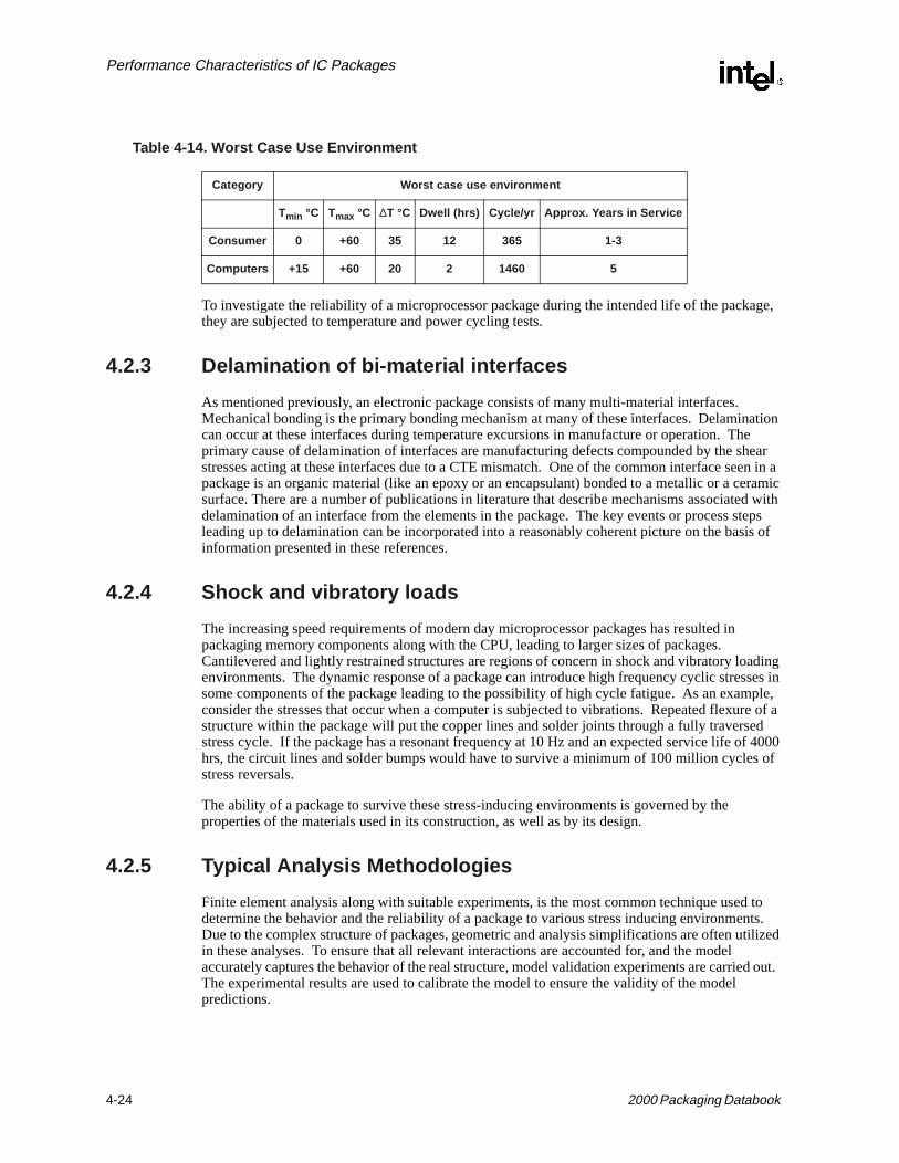
A microprocessor package is subjected to numerous heating and cooling cycles in operationWhen the device is powered up, its temperature rises, and when it is shut down, its temperadrops. The magnitude of the maximum temperature on the die surface depends on the thersolution employed, and is usually between 80 to 125°C. In addition to these power on and poff cycles (maxi-cycles), the microprocessor is cycled between different intermediate tempervalues depending upon processor usage (mini-cycles) in any application program. The InstituInterconnecting and Packaging Electronic Circuits [2] lists the typical worst case usage condfor personal computers and consumer electronics as given below. This table is intended onlguideline, and individual companies use different field use conditions based on their researc
2000 Packaging Databook 4-23
Performance Characteristics of IC Packages
Table 4-14. Worst Case Use Environment
To investigate the reliability of a microprocessor package during the intended life of the package, they are subjected to temperature and power cycling tests.
4.2.3 Delamination of bi-material interfaces
As mentioned previously, an electronic package consists of many multi-material interfaces. Mechanical bonding is the primary bonding mechanism at many of these interfaces. Delamination can occur at these interfaces during temperature excursions in manufacture or operation. The primary cause of delamination of interfaces are manufacturing defects compounded by the shear stresses acting at these interfaces due to a CTE mismatch. One of the common interface seen in a package is an organic material (like an epoxy or an encapsulant) bonded to a metallic or a ceramic surface. There are a number of publications in literature that describe mechanisms associated with delamination of an interface from the elements in the package. The key events or process steps leading up to delamination can be incorporated into a reasonably coherent picture on the basis of information presented in these references.
4.2.4 Shock and vibratory loads
The increasing speed requirements of modern day microprocessor packages has resulted in packaging memory components along with the CPU, leading to larger sizes of packages. Cantilevered and lightly restrained structures are regions of concern in shock and vibratory loading environments. The dynamic response of a package can introduce high frequency cyclic stresses in some components of the package leading to the possibility of high cycle fatigue. As an example, consider the stresses that occur when a computer is subjected to vibrations. Repeated flexure of a structure within the package will put the copper lines and solder joints through a fully traversed stress cycle. If the package has a resonant frequency at 10 Hz and an expected service life of 4000 hrs, the circuit lines and solder bumps would have to survive a minimum of 100 million cycles of stress reversals.
The ability of a package to survive these stress-inducing environments is governed by the properties of the materials used in its construction, as well as by its design.
4.2.5 Typical Analysis Methodologies
Finite element analysis along with suitable experiments, is the most common technique used to determine the behavior and the reliability of a package to various stress inducing environments. Due to the complex structure of packages, geometric and analysis simplifications are often utilized in these analyses. To ensure that all relevant interactions are accounted for, and the model accurately captures the behavior of the real structure, model validation experiments are carried out. The experimental results are used to calibrate the model to ensure the validity of the model predictions.
Category Worst case use environment
Tmin °C Tmax °C ∆T °C Dwell (hrs) Cycle/yr Approx. Years in Service
Consumer 0 +60 35 12 365 1-3
Computers +15 +60 20 2 1460 5
4-24 2000 Packaging Databook

Performance Characteristics of IC Packages
ared e in-e be
ed to nd the e size
d to be ture.
good
In recent years, extremely sensitive, full-field optical interference techniques have been extensively used to calibrate and compare numerical predictions to actual behavior. Some of the commonly employed "opto-mechanical tools" that produce high-resolution, full-field contour maps of thermo-mechanical deformation within an electronic package are Moiré Interferometry, Infr(IR) Fizeau Interferometry and Shadow Moiré [3-5]. While Moire interferometry measures thplane deformation, Fizeau interferometry and Shadow moire are used to map the out of plandeformation (warpage) of packages. In addition to model validation, these tools by itself canused to study the effect of design changes on the behavior of the package quickly.
4.2.5.1 Numerical analysis and model validation examples
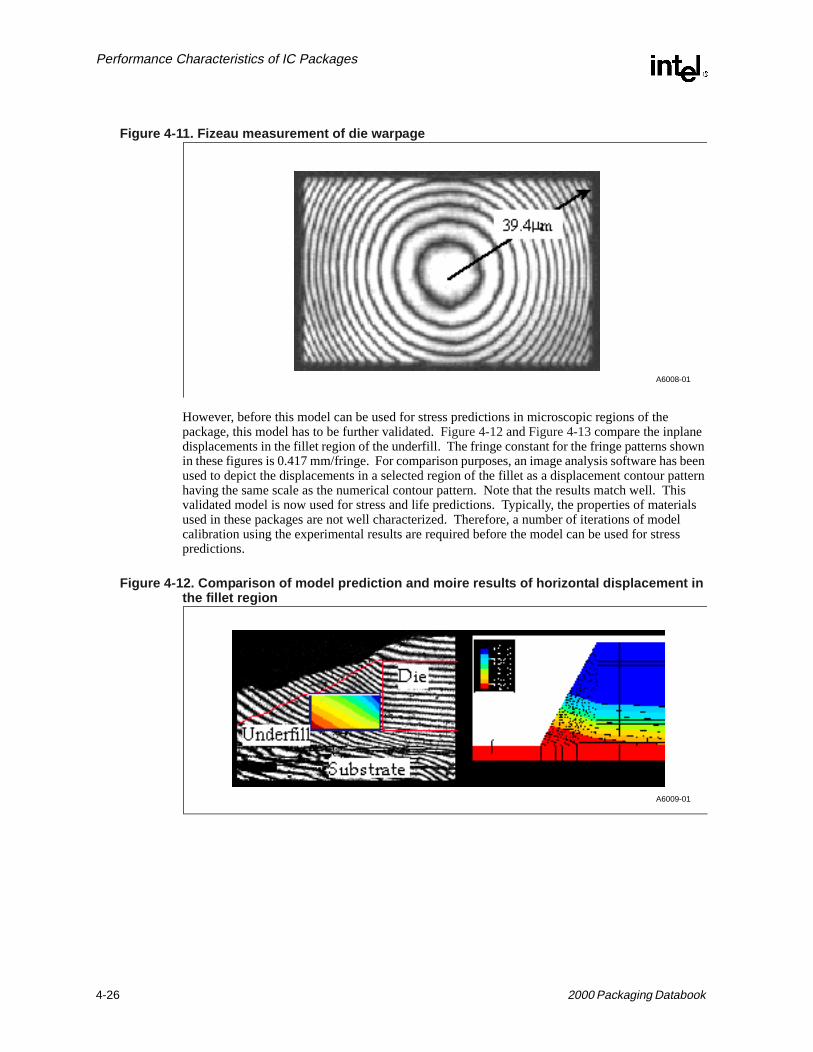
Figure 4-10 shows a finite element model and the out of plane displacement of a C4 die bonda substrate after assembly. Since there is a CTE mismatch between the silicon, substrate, adie attach materials, the assembly warps after cool-down from the reflow temperature. For thof the assembly modeled, the out of plane displacement on the surface of the die is predicte39.45 microns. Figure 4-11 shows the Fizeau measurement of the die warpage after manufacThe fringe sensitivity of this measurement is 2.65 um/fringe, which gives the total warpage (measured from center to corner) on the die surface to be 39.4 microns. Note that there is acorrelation between the numerical prediction and the experimental measurement, thereby, validating the general behavior of the finite element model.
Figure 4-10. Finite element model and out of plane displacement of a die C4 attached to a substrate
A6007-01
2000 Packaging Databook 4-25
Performance Characteristics of IC Packages
Figure 4-11. Fizeau measurement of die warpage
However, before this model can be used for stress predictions in microscopic regions of the package, this model has to be further validated. Figure 4-12 and Figure 4-13 compare the inplane displacements in the fillet region of the underfill. The fringe constant for the fringe patterns shown in these figures is 0.417 mm/fringe. For comparison purposes, an image analysis software has been used to depict the displacements in a selected region of the fillet as a displacement contour pattern having the same scale as the numerical contour pattern. Note that the results match well. This validated model is now used for stress and life predictions. Typically, the properties of materials used in these packages are not well characterized. Therefore, a number of iterations of model calibration using the experimental results are required before the model can be used for stress predictions.
Figure 4-12. Comparison of model prediction and moire results of horizontal displacement in the fillet region
A6008-01
A6009-01
4-26 2000 Packaging Databook

Performance Characteristics of IC Packages
)
but m a
eel ients
e
Figure 4-13. Comparison of model prediction and moire results of verticle displacement in the fillet region
Besides it’s use as model validation tools, these interferometric techniques are also used to compare materials and design options, due to its relatively short time-to-data. Two epoxy samples proposed to be used as the encapsulant material in PLGA (Plastic Land Grid Arraypackages were compared using Moire interferometry. In PLGA packages, the silicon die is covered with the encapsulated. This epoxy not only covers the active surface of the silicon, also the wire-to-pad interconnects. Therefore, these two epoxy samples were compared frowire bond reliability perspective.
Figure 4-14 compares the Moiré U-field displacement patterns (horizontal fields) of the wire hregion (at the wire to die interface) using the two different encapsulant materials. Fringe gradin any direction would indicate relative motion between the encapsulant and the die in that direction, increasing the likelihood of failure during temperature excursions. V-field images (vertical field) revealed almost no fringe gradients in the wire heel region indicating negligiblrelative motion between the die and the encapsulant in that direction.
Figure 4-14. Comparison of horizontal displacement fields in the wirebond region of PLGA.
Note the higher density of fringes in the right image
A6010-01
A6011-01
Encapsulant Sample A Encapsulant Sample B
2000 Packaging Databook 4-27

Performance Characteristics of IC Packages
eel
ing e gth
re
lding tors ced to
sweep
lead hermal ts from
d
Figure 4-15. Comparison of free expansions of the two encapsulant materials used in the study
However as shown in Figure 4-14, the horizontal displacement of the the encapsulant in wire heel area of the sample using encapsulant B is twice that in the case of the package using sample A. This difference in behavior between encapsulant A and B was confounding since both encapsulants had nearly identical bulk CTE’s in the horizontal direction. The encapsulant material in the harea of both packages were seperated and moire performed. Figure 4-15 shows the horizontal displacement fields obtained from both encapsulant materials. Figure 4-15 indicates that encapsulant B has a much larger CTE at the interface that encapsulant A. This was later determined to be due to a lower filler content at the interface.
4.2.6 Surface Mounted Lead Packages
4.2.6.1 Bond Stresses
In addition to the mechanical and metallurgical stresses developed during the wire-bonding process, encapsulation and environmental stresses subsequent to bonding can contribute todegradation of the interconnection. Reliable first and second bonds can be ensured by bondwithin the process windows for force, power, time, and temperature. Excursions beyond theswindows are minimized through regular process monitors such as bond pulls. Both pull strenand failure mechanism criteria must meet specifications. In particular, no cratering failures aacceptable even if pull strength criteria are met, since craters indicate excessive force duringbonding which could lead to reliability problems in the field.
During encapsulation, wire sweep may occur if wire lengths are too great or if drag during moflow is excessive. Current mold gate designs provide low drag flow patterns, and X-ray moniare used to confirm process stability. Wire diameter and length design rules are strictly enforensure that there is adequate mechanical stability of the bond arch to resist drag forces. Development of new package designs includes analysis and experiment to ensure that wire is minimized.
In plastic packages, delamination at the interface between molding compound and silicon orframe can cause high stresses at the first or second bond location, because the differential texpansions must be accommodated across the bond itself. The delamination generally resultemperature cycling of packages with trapped moisture. To suppress the adverse effects of delamination, selection of materials with enhanced interfacial adhesion and the design of lea
A6012-01
Sample A Sample B
4-28 2000 Packaging Databook
Performance Characteristics of IC Packages
55° C ition of design
-n in FR–
frames that feature additional mold compound locking characteristics have proven to be effective. Finite element models are used to guide and optimize designs. For packages that are particularly moisture-sensitive, shipment of prebaked product in sealed moisture-proof bags with desiccant ensures that delamination is minimized and operation of the assembled part will be reliable.
4.2.6.2 Compliant Leads and Solder Joint Fatigue
With the advent of surface mounted packages, solder joint integrity became an issue of considerable concern. It was found that solder joints on leadless ceramic packages measuring more than 0.5 inch on a side could survive only a few hundred temperature cycles (Condition B, –to +125° C) when the packages were surface mounted to FR–4–type circuit boards. The addcompliant leads to these packages has extended the life considerably and is now used in theof all new surface mounted packages.
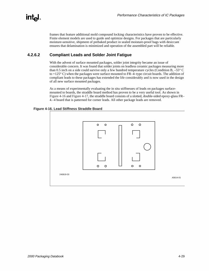
As a means of experimentally evaluating the in situ stiffnesses of leads on packages surfacemounted to boards, the straddle board method has proven to be a very useful tool. As showFigure 4-16 and Figure 4-17, the straddle board consists of a slotted, double-sided epoxy-glass4.–4 board that is patterned for corner leads. All other package leads are removed.
Figure 4-16. Lead Stiffness Straddle Board
A5614-01
240819-20
2000 Packaging Databook 4-29

Performance Characteristics of IC Packages
ing on
l cycles ing
shown
Figure 4-17. Straddle Board with Two Packages in Place
Units are mounted on both sides of the board using production-level processes and specifications for each package. The board is mounted vertically in a tensile test set-up such as a materials test system (MTS), and the narrow sides of the slot are cut, separating the two ends of the package. The MTS is fitted with a 200 lb. load cell and a 6 inch displacement actuator. This allows the straddle board to be tested with a 0.020 inch displacement, 0.010 inch in the tensile cycle and 0.010 inch in the compressive cycle. These values were chosen to span the lead displacement experienced during temperature excursions from –65° C to +150° C (MIL–STD–883C T/C [C]).
A total cycle time of five seconds was used with a maximum load range of 0.8-8 lbs., dependthe package type and lead count. As Figure 4-18 shows, leads are loaded in both lateral and transverse directions (i.e. in the plane and normal to the plane of the lead bend). Twenty-fivesamples per lead count per direction were evaluated. Once the board was mounted, three fulwere run, and the force versus deflection curve was recorded. The linear portions of the loadand unloading curves were used to determine the lead stiffness. A typical hysteresis curve isin Figure 4-19.
Figure 4-18. Orientation of Applied Load
A5615-01
240818-21
Force Force
Transverse Mount Lateral Mount
A5616-01240819-62
4-30 2000 Packaging Databook

Performance Characteristics of IC Packages
S 3–D to the
re
the port d
the QFP sult
iated
re is values OP,
n rest, portant along tion in ent
stress high the
level e to
Figure 4-19. Lead Stiffness Determined from Hysterisis
Designing leads with adequate compliance is now recognized as an important element of overall product design, and mechanical modeling has proven to be a useful design tool. Lateral and transverse lead stiffnesses were calculated for PLCC, and PQFP packages using the ANSYelastic beam element option. The calculated stiffness for each type of package was matchedvalue obtained from the straddle board measurements by locating the point on the lead wheagreement was reached. In all cases, the point lay within the solder joint, in agreement with physical expectations.
Of particular interest were the boundary conditions imposed by the solder joint on the foot oflead. In the lateral direction, the solder volume is adequate for the joint to provide built-in supto the lead foot (zero rotation). However, in the transverse direction for the PLCC and cerquapackages, the J-bend lead stiffnesses are large enough to produce inelastic deformations insolder joint. As a result, the joint acts like a pinned support (free rotation). In all cases, the Pgull-wing leads are sufficiently compliant for the solder joint to act as a built-in support. This resuggests that reducing lead stiffness will significantly reduce solder joint stresses and assoccreep and fatigue. Experimental data recently reported in supports this hypothesis.
Because of the contribution of lead stiffness to the level of stress in the solder joint when thethermal mismatch between package and board, a comprehensive list of in situ lead stiffnessis provided in Figure 4-21. All surface mounted packages currently used for Intel products (TSPLCC, PQFP and CQFP) are listed in Table 4-15. For these packages both translational and rotational stiffness components are given. The translational stiffness is defined as the force ipounds created by a displacement in inches applied at the solder joint in the direction of intethe remaining force and rotation components being zero. These stiffness components are imwhen the thermal mismatch creates differential displacements which must be accommodatedthe leads. The rotational stiffness is defined as the moment in inch-pounds created by a rotaradians applied at the solder joint about the axis of interest, all other moments and displacemcomponents being zero. These stiffness components are important when thermally induced differential rotations are imposed at the ends of the leads.
The magnitude of the stiffness components are useful in making comparisons of the level ofor strain induced in the solder joint by various package types; high lead stiffness will generatesolder stresses, etc. Experience to date indicates that in situ translational lead stiffnesses onorder of 100 lb./in. or less produce excellent joint reliability. Even lead stiffnesses above thisare acceptable although they have less margin than the more compliant leads. With referenc
A5617-01
0.010*-0.005*-0.010*
Load
(LS
B)
Dissplacement (IN.)240819-23
4.0
3.0
2.0
1.0
-1.0
-2.0
-3.0
-4.0
0.005*
2000 Packaging Databook 4-31

Performance Characteristics of IC Packages
rtance
nt lead r the
ms in
kage d upon
ckage.
y the
verses
P II design. cle (T/
Figure 4-21, the x– and y–components of the gull-wing leads on 0.025 in. centers (PQFP andCQFP) fall into this category. The z-components are always large and demonstrate the impoof minimizing board flexing, which generates these z-components.
To assist in visualizing the stiffness and stress entries in Table 4-15, Figure 4-21 has been prepared.The gull-wing lead of the PQFP has been used for reference. In all entries, the center line represents the lead profile in the plane of interest. The heavy line represents the displacemeprofile associated with the displacement or rotation component indicated at the point on the connected to the solder. The line connected by shading to the undeflected profile shows thedistribution of the bending stress along the lead. In general, the maximum value is at or neasolder connection point; however, for displacements along (or rotations about) the z-axis, thebending stress maximizes at the package body. As mentioned previously, z-component displacements may generate high lead stresses. Figure 4-21 suggests that the package body is thesite of maximum stress and damage in the lead.
Under certain conditions, stresses in the lead may be large enough to cause reliability problethe lead as well as in the solder joint. The figures of merit presented in Table 4-16 extracted from Table 4-15, provides indicators of lead compliance and lead stress levels for current Intel pactypes. All the lead compliance and stress of various packages and lead designs are normalizethe lead configuration of a 68L PLCC package. The first two columns give the level of lead compliance along the lateral and transverse directions as compared to that of a 68L PLCC paThe lead stress is estimated by applying a unit displacement (1 mil) along the lateral or the transverse direction, the third and fourth columns provide the level of lead stress produced bproposed lead displacement. A correlation between the lead stiffness and the lead stress is observed; the greater the lead stiffness, the higher the lead stress. A plot of log [lead stress]log [lead stiffness] is shown in Figure 4-20. The trend of the lead stress dependence on lead stiffness is linear on a log-log plot for most of the Intel packages except the TSOP I and TSOpackages which show much stiffer lead response because of their low profile and short lead In general, a stiffer lead will introduce higher stress at the solder joint during temperature cy
Table 4-15. Surface Mount Package Lead Stiffness
Lead Stiffness Components Maximum Lead Stresses
PackageTrans. Stiffness
(lb/in.)Rotation Stiffness
(in.-lb/rad.)Trans. Stresses
(Ksi/m in.)Rot. Stresses(Ksi/m rad.)
Type Kx Ky Kz Kθx Kθy Kθz σx σy σz σθx σθy σθz
TSOP(I) 1900 2560 9730 0.579 0.435 0.115 514 521 1660* 7.89 9.55 1.78*
TSOP(II) 3820 18800 19500 4.42 0.869 0.704 514 990 1660* 15.1 9.55 2.86*
PLCC 44L 323 1250 7750 1.82 0.379 1.03 43.3 59.1 335 1.81+ 6.65 1.56+
PLCC 68L 187 1190 8813 1.03 0.166 0.641 43.7 89.1 474 3.08+ 6.99 2.60+
PQFP 39.8 85.9 955 0.245 0.133 0.0468 30.4 35.9 281* 1.98 2.05 0.438*
CQFP 9.05 23.0 250 0.361 0.0132 0.0232 16.6 24.8 173* 2.39 1.62 0.342*
DEFINITIONS: Kα = Force in lbs. needed to produce a displacement in inches in the α direction at the solder joint, all other forces and rota-tions = 0.Kθα = Moment in in-lbs. needed to produce a rotation in rad. about the α axis at the solder joint, all other moments and dis-placements = 0.σα = Maximum lead stress in Ksi due to a 0.001 in. displacement in the α direction at the solder joint, all other forces and rotations = 0. Unless otherwise noted, maximum stress occurs at the solder joint.σθα = Maximum lead stress in Ksi due to a 0.001 rad. rotation about the α axis at the solder joint, all other forces and rota-tions = 0. Unless otherwise noted, maximum stress occurs at the solder joint.x = Outward normal to the edge of the package in the plane of the unformed leadframe.y = Tangent to the edge of the package in the plane of the unformed leadframe.z = Perpendicular to the plane of the unformed leadframe.NOTES: 1. * Maximum at the package body.2. + Maximum at the site of lead width reduction.
4-32 2000 Packaging Databook

Performance Characteristics of IC Packages
C) stressing and subsequently degrades the solder joint fatigue performance. To assess solder joint reliability, a methodology is described in the following paragraphs to investigate the solder joint fatigue performance at various lead displacement amplitudes and frequencies.
Figure 4-20. Lead Stress Dependence on Lead Stiffness for Various Lead Designs
Table 4-16. Figures of Merit for Lead Compliance and Lead Stress Package
Compliance FOM 1 Stress FOM 2
Package Lateral Transverse Lateral Transverse
TSOP I 0.098 0.46 0.085 0.17
TSOP II 0.049 0.06 0.085 0.09
44L PLCC 0.58 0.95 1.01 1.51
68L PLCC 3 1.00 1.00 1.00 1.00
100L PQFP 4.70 13.85 1.44 2.48
CQFP 20.66 51.74 2.73 3.59
NOTES: 1. Compliance FOM = (Package Compliance) / (68L PLCC Compliance).2. Stress FOM = (68L PLCC Lead Stress) / (Package Lead Stress).3. 68L PLCC: Lateral Lead Stiffness = 187 lbf/in, Transverse Lead Stiffness = 1190 lbf/in.4. Lateral Lead Stress = 43.7 Kpsi/mil, Transverse Lead Stress = 89.1 Kpsi/mil.
A5618-01240819-48
CQ (L)
CQ (T)
PQ (L)PQ (T)
Cd (L)
PL68 (L)
PL44 (L)PL44 (T)
Log [Lead Stiffness (lbg / in.)]
PL68 (T)
Cd (T)
TSI (L) TSII (L)
TSI (T)TSII (T)
4.543.532.521.510.501.2
1.4
1.6
1.8
2
2.2
3
2.8
2.6
2.4
CQ : CQFP Package, (L) : Lateral, (T) : Transverse.
PQ : PQFP Package, (L) : Lateral, (T) : Transverse.
Cd : Cerquad package, (L) Lateral, (T) : Transverse.
PL68 : 68L PLCC Package, (L) : Lateral, (T) : Transverse.
PL44 : 44L PLCC Package, (L) : Lateral, (T) : Transverse.
TSI : TSOP (I) Package, (L) : Lateral, (T) : Transverse.
TSII : TSOP (II) Package, (L) : Lateral, (T) : Transverse.
2000 Packaging Databook 4-33

Performance Characteristics of IC Packages
Figure 4-21. Stress Distribution along a PQFP Lead
A5619-01240819-44
Z
YX
Z
Y X
Z
Y X
Z
YX
Sigmax UYUX
Sigmax
Sigmax
UZRotx
Sigmax
4-34 2000 Packaging Databook

Performance Characteristics of IC Packages
the c nents ent red. is ng
during
n
cement nergy
Figure 4-22. Stress Distribution Along a PQFP Lead (continued)
4.2.6.3 Effects of Loading Frequency and Amplitude on Solder Joint Damage
Cyclic strain energy dissipation, W, was analyzed for a simple two segment structure consisting of solder exhibiting elastic, plastic and creep behavior connected in series with copper exhibiting elastic behavior only. The structure is fixed at one end and subjected to a ‘square wave’ displacement at the other. The total strain energy consists of plastic and creep components,magnitudes of which depend on the amplitude and frequency of the square wave. The plasticomponents arise during the instantaneous changes in displacement while the creep compooccur during the dwell periods. At very low frequencies (long dwell times), the creep componprovides maximum contribution to the total, in the range of 15-50% for the examples consideAt very high frequencies (very short dwell times), only the plastic component contributes andsmaller than its low-frequency counterpart. This is because the creep relaxation during the lodwell period at the low frequency end enables a large value of plastic strain to be generatedthe instantaneous change in displacement following the dwell.
A quantitative picture of the dependence of the total strain energy dissipation, W, per cycle odisplacement amplitude and frequency is shown in Figure 4-23 and re-mapped to Figure 4-24. These iso-strain energy dissipation contours per cycle show strong dependence on the displaamplitude and weaker dependence on the cyclic frequency. The use of the cumulated total ecould provide reasonably good prediction on the solder joint fatigue life. The use of this methodology to predict a 68 L PLCC solder joint reliability is described in the next section.
Z
Y
X
Sigmax
Rotz
Z
X Y
Sigmax
Roty
A5620-01240819-46
2000 Packaging Databook 4-35

Performance Characteristics of IC Packages
of the d and on at for
ch is
Figure 4-23. Dependence of Total Strain Energy Dissipation per Cycle on Displacement Amplitude and Frequency
Figure 4-24. Isocontours of Strain Energy Dissipation in Displacement Amplitude and Frequency Space
4.2.6.4 Dependence of J-Lead Solder Joint Reliability on Lead Displacement Amplitude and Frequency
A 68L PLCC configuration was selected to study the J-lead solder joint reliability as a function of lead displacement amplitude (d) and frequency (t) (period of fatigue cycle). The general form of the constitutive relations for the solder and the lead is given elsewhere. A “square wave” displacement amplitude of 1.25-5 mils and periods of 0-30 minutes were applied to the end lead, the total inelastic energy dissipation (plastic and creep) in the solder joint was analyzedisplayed in Figure 4-25. The total energy, W, exhibits a monotonically increasing dependencethe lead displacement (d) and frequency (t) (period of fatigue cycle). In addition, it appears tha given displacement, the total energy, W, asymptotically approaches a maximum value whireasonably well approximated by W at t = 30 minutes.
35
30
25
20
15
10
5
00 0.2 0.4 0.6 0.8 1.0 1.2
D (10 in.)-3
Wf (
Ib.-
in/in
)
3
Wt = Inelastic Strain Energy f = Fatigue Cycle FrequencyD = Displacement
Wheref (Min )--1
0.0625
1.02.0
0.250.5
A5621-01240818-49
0.125
Wt = Inelastic Strain Energy f = Fatigue Cycle FrequencyD = Displacement
Where 1.2
1.0
0.8
0.6
0.4
0.2
00 0.2 0.4 0.6 0.8 1.0 1.2 1.4 1.6 1.8 2.0
Wt (Ib-in / in )3
80
160
402010
f (Min )-1
D (
10
In.)
-3
A5622-01240819-50
4-36 2000 Packaging Databook
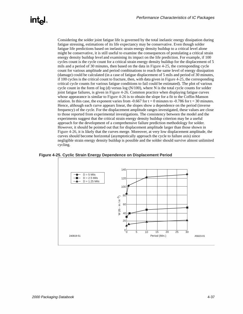
Performance Characteristics of IC Packages
Considering the solder joint fatigue life is governed by the total inelastic energy dissipation during fatigue stressing, estimations of its life expectancy may be conservative. Even though solder fatigue life predictions based on inelastic strain energy density buildup to a critical level alone might be conservative, it is still useful to examine the consequences of postulating a critical strain energy density buildup level and examining its impact on the life prediction. For example, if 100 cycles count is the cycle count for a critical strain energy density buildup for the displacement of 5 mils and a period of 30 minutes, then based on the data in Figure 4-25, the corresponding cycle count for various amplitude and period combinations to reach the same level of energy dissipation (damage) could be calculated (in a case of fatigue displacement of 5 mils and period of 30 minutes, if 100 cycles is the critical count to fracture, then, with data given in Figure 4-25, the corresponding critical cycle counts for various fatigue conditions to fail could be estimated). The plot of various cycle count in the form of log (d) versus log (N/100), where N is the total cycle counts for solder joint fatigue failures, is given in Figure 4-26. Common practice when displaying fatigue curves whose appearance is similar to Figure 4-26 is to obtain the slope for a fit to the Coffin-Manson relation. In this case, the exponent varies from -0.667 for t = 0 minutes to -0.786 for t = 30 minutes. Hence, although each curve appears linear, the slopes show a dependence on the period (inverse frequency) of the cycle. For the displacement amplitude ranges investigated, these values are close to those reported from experimental investigations. The consistency between the model and the experiments suggest that the critical strain energy density buildup criterion may be a useful approach for the development of a comprehensive failure prediction methodology for solder. However, it should be pointed out that for displacement amplitude larger than those shown in Figure 4-26, it is likely that the curves merge. Moreover, at very low displacement amplitude, the curves should become horizontal (asymptotically approach the cycle to failure axis) since negligible strain energy density buildup is possible and the solder should survive almost unlimited cycling.
Figure 4-25. Cyclic Strain Energy Dependence on Displacement Period
D = 5 MilsD = 2.5 MilsD = 1.25 Mils
0 5 10 15 20 25 300
20
40
60
80
100
140
120
W (
Ib -
in /
in
)-3
Period (Min.) A5623-01240819-51
2000 Packaging Databook 4-37

Performance Characteristics of IC Packages
Figure 4-26. Dependence of Log of Displacement Amplitude on Log of (N/100) for Different Displacement Periods
4.3 IC Package Thermal Characteristics
4.3.1 Importance of Thermal Management
Thermal management of an electronic system encompasses all the thermal processes and technologies that must be utilized to move and transport heat from individual components to the system thermal sink in a controlled manner.
Thermal management has two primary objectives. The first is to ensure that the temperature of each component is maintained within both its functional and maximum allowable limit. The functional temperature limit defines the maximum temperature up to which the electrical circuits may be expected to meet their specified performance targets. Operation of the circuits at temperatures higher than the functional limit may result in performance degradation or logic errors. The maximum allowable temperature limit is the highest temperature to which a component or part thereof may be safely exposed. Operation of the component at temperatures higher than the maximum allowable temperature limit may cause irreversible changes in its operating characteristics or may even cause physical destruction of the component.
The second objective of thermal management is to ensure that the temperature distribution in each component satisfies reliability objectives. Failure mechanisms encountered in electronic components are kinetic in nature and depend exponentially on the device operating temperature. The exact relationship between the failure rate and temperature depends upon the thermophysical properties of the packaging materials and the failure mechanism in operation. The relationship between the normalized failure rate and temperature, for changes in the device operating characteristics resulting from chemical or diffusive processes, can be defined by an Arrhenius equation as follows:
Tau = 0 Min.Tau = 1 Min.Tau = 2.5 MinTau = 30 Min.
0.7
0.6
0.5
0.4
0.3
0.2
0.1
00 0.2 0.4 0.6 0.8 1 1.2
Log N / 100
Log
D (
Mils
)
A5624-01240819-52
4-38 2000 Packaging Databook

Performance Characteristics of IC Packages
0.8 in an
Equation 4-11.
Where:
Figure 4-27 shows a plot of Equation 4-11 for a reference temperature of 100 °C and activationenergies of 0.4 eV to 1.0 eV. The figure shows that for activation energies between 0.6 eV toeV, a 25 °C increase in the operating temperature, above the reference temperature, resultsapproximately five to six fold increase in the failure rate. Thus, precise control of componentoperating temperatures is absolutely essential to ensure product reliability.
Figure 4-27. Component Failure Rate as a Function of Junction Temperature
θn
θTθTr--------- Exp
EA
k-------
1Tr------ 1
T---–
= =
θ = Failure rate
θn = Normalized failure rate
T = Absolute junction temperature (K)
Tr = Reference temperature (K)
EA = Activation energy (eV)
k = Boltzmann’s constant: 8.616 X 10⁻⁵ (eV/K)
160150140100 110 120 130
10
100
AE = 1 eV
AE = 0.8 eV
AE = 0.6 eV
AE = 0.4 eV
Junction Temperature (˚C)
Nor
mal
ized
Fai
lure
Rat
e
A5625-01240819-24
2000 Packaging Databook 4-39

Performance Characteristics of IC Packages
4.3.2 Heat Transfer Modes
To understand the thermal characteristics of electronic components and packages, it is necessary to briefly review the processes by which heat is transferred from one point to another. Heat transfer occurs via one or more of three modes: conduction, convection, and radiation.Conduction
4.3.2.1 Conduction
Conduction is a mode of heat transfer in which heat flows from a region of higher temperature to one of lower temperature within a medium (solid, liquid, or gaseous) or media in direct physical contact. In conductive heat flow, the energy is transmitted by direct molecular communication without appreciable displacement of the molecules.
In a one-dimensional system (see Figure 4-22), conductive heat transfer is governed by the following relation:
Equation 4-12.
where:
Equation 4-12 indicates that in conduction, the heat flow rate is directly proportional to material thermal conductivity, temperature gradient, and cross-sectional area. Equation 4-12 can be written as:
Equation 4-13.
Using an electrical analogy, if q and T are analogous to current and voltage respectively, L/kA is analogous to electrical resistance. According to Equation 4-13, thermal resistance can be expressed in terms of material thermal conductivity and geometrical parameters and is independent of the power dissipation.
q -kA=∆TL
------- KAT1 T2–
L-----------------–=
q = Heat flow rate (W)
k = Material thermal conductivity (W/mC)
A = Cross-sectional area (m2)
T = Temperature difference, T1-T2, between the hot and cold regions (K or °C)
L = Linear distance between the locations of T1-T2 (m)
∆
q =∆ T
L kA⁄--------------
∆
4-40 2000 Packaging Databook

Performance Characteristics of IC Packages
Figure 4-28. One-Dimensional Heat Flow by Conduction
4.3.2.2 Convection
Convection is a mode of heat transport from a solid surface to a fluid and occurs due to the bulk motion of the fluid. The basic relation that describes heat transfer by convection from a surface presumes a linear dependence on the surface temperature rise over the ambient, and is referred to as Newton’s law of cooling:
Equation 4-14.
where:
Equation 4-14 can also be written as:
Equation 4-15.
Comparing Equation 4-15 to Equation 4-14, it is apparent that the convective thermal resistancecan be defined as 1/hcA.
L
q
T1 T2 A5630-01240819-29
qc hc A Ts Ta–( )=
qc = Convective heat flow rate from a surface to ambient (W)
A = Surface area (m2)
Ts = Surface temperature (C)
Ta = Average convective heat transfer coefficient
hc = Average convective heat transfer coefficient (W/m2C)
qc
Ts Ta–
1 hcA⁄------------------=
2000 Packaging Databook 4-41

Performance Characteristics of IC Packages
In forced convection, fluid flow is created by an external factor such as a fan. In free or natural convection, fluid motion is induced by density variations resulting from temperature gradients in the fluid. Under the influence of gravity or other body forces, these density differences give rise to buoyancy forces that circulate the fluid and convect heat toward or away from surfaces wetted by the fluid.
4.3.2.3 Radiation
Radiation heat transfer occurs as a result of radiant energy emitted from a body by virtue of its temperature. Radiation heat transport occurs without the aid of any intervening medium. Radiant energy is sometimes envisioned to be transported by electromagnetic waves, at other times by photons. Neither viewpoint completely describes the nature of all observed phenomena.
The amount of heat transferred by radiation, between two surfaces at temperatures T1 and T2 respectively, is governed by the following expression:
Equation 4-16.
where:
Note that the temperatures T1 and T2 in Equation 4-16 are absolute temperatures.
For radiation to make a rather significant contribution compared to either natural convection or forced convection mechanisms, a relatively large temperature difference must exist between T1 and T2. In the case of most low-power electronic applications, these temperature differences are relatively small and, therefore, radiation effects are normally neglected. But for power application, heat transfer by radiation should be considered. To compare radiative and convective effects, a radiation heat transfer coefficient is defined as:
Equation 4-17.
where hr is a radiative heat transfer coefficient.
4.3.3 Thermal Resistance in Packaging Design
The thermal performance of IC packages is typically measured using the junction-to-ambient and junction-to-case thermal resistance values. These parameters are defined by the following relations:
q ∈ σ A T14 T24–( ) F12=
q = Amount of heat transfer by radiation (W)
∈ = Emissivity (0 < ∈ < 1)
σ = Stefan-Boltzmann constant, 5.67 X 10⁻⁸ (W/m2 K4)
A = Area (m2)
F12 = Shape factor between surfaces 1 and 2 (A fraction of surface 1 radiation seen by surface 2)
T1, T2 = T1, T2 = Surface temperatures (K)
hr ∈σF12 T12 T22–( ) T1 T2+( )=
4-42 2000 Packaging Databook

Performance Characteristics of IC Packages
Equation 4-18.
Where:
The junction-to-case thermal resistance, θjc, is a measure of the internal thermal resistance of the package from the silicon die to the package exterior. θjc is strongly dependent on the thermal properties (i.e. thermal conductivities) of the packaging materials and on the package geometry. The junction-to-ambient thermal resistance, θja, includes not only the package internal thermal resistance, but also the conductive and convective thermal resistance from package exterior to the ambient. θja values depend on material thermal conductivities, package geometry as well as ambient conditions such as coolant flow rates and the thermophysical properties of the coolant.
To guarantee component functionality and long-term reliability, the maximum device operating temperature is bounded by setting constraints on either the ambient temperature or the package exterior temperature measured at predefined locations. Ambient temperature is most often measured at an undisturbed location at a certain distance away from the package. As defined in Intel experiments, the case temperature is measured at the center of the top surface of the package. Depending on the environment (ambient and board temperatures) within the computer system, thermal enhancements such as fins or forced air cooling may be necessary to meet requirements on the package case temperature, "Tc".
4.3.4 Factors Impacting Package Thermal Resistance
The thermal resistance of a package is not a constant. Package mounting configuration and many packaging and environmental parameters have an impact on the thermal resistance values. The following is a summary of some parameters which affect thermal resistance.
4.3.4.1 Package Size
As shown by the one-dimensional conductive and convective thermal resistance expressions (see Equation 4-14 and Equation 4-16), thermal resistance is inversely proportional to area. This means that as the package gets larger, the thermal resistance becomes smaller due to an increase in the
θjC
Tj Tc–P
-----------------=
θcaTc Ta–
P------------------=
θja θjc θca+=
θja = Junction-to-ambient thermal resistance (C/W)
θjc = Junction-to-case thermal resistance (C/W)
θca = Case-to-ambient thermal resistance (C/W)
Tj = Average die temperature (C)
Tc = Case temperature at a predefined location (C)
P = Device Power dissipation (W)
Ta = Ambient temperature (C)
2000 Packaging Databook 4-43

Performance Characteristics of IC Packages
heat transfer area. Figure 4-29 through Figure 4-31 show typical junction-to-ambient thermal resistance values as a function of lead count for different package families. According to this figure, thermal resistance is lower for packages with higher lead counts (i.e. larger package size) within the same package family.
Figure 4-29. Effect of Package Size on Thermal Resistance of PLCC, PQFP, and PGA Packages
Figure 4-30. Effect of Package Size on Thermal Resistance of Plastic and Ceramic Dual-In-Line Packages
0 100 150 200 250 300
Package Lead Count
0
10
20
30
40
50
60
70
Junc
tion-
to-A
mbi
ent T
herm
al R
esis
tanc
e (C
/W)NOTE: Pin Grid
and Plastic Surface Mount Packages
PQFPPLCCPGA (No Spreader)PGA (With Spreader)SPGA (No Spreader)SPGA (With Spreader)
A5631-01240819-30
50
A5632-01240819-31
160
140
120
100
80
60
40
20
05040302010
Side - Brazed CeramicCerdipPlastic / Alloy 42Plastic / Copper
Lead Count
Junc
tion
- T
o -
Am
bien
tT
herm
al R
esis
tanc
e (C
/ W
)
4-44 2000 Packaging Databook

Performance Characteristics of IC Packages
Figure 4-31. Effect of Package Size on Thermal Resistance of Leadless Ceramic Chip Carrier
4.3.4.2 Packaging Material Thermal Conductivity
Again, the one-dimensional conductive thermal resistance expression shows that thermal resistance is inversely proportional to the thermal conductivity of the packaging material. For example, aluminum oxide, the most commonly used ceramic material, has a thermal conductivity that is an order of magnitude larger than plastic materials. As a result, the internal resistance of a ceramic package is substantially lower than a plastic package from the same package family, resulting in lower overall thermal resistance (see Figure 4-32, CQFP versus PQFP).
Figure 4-32. Effect of Packaging Material on Thermal Resistance
A5633-01240819-32
LCCC
30 40 50 60 70
Lead Count
Junc
tion
- To
- A
mbi
ent
The
rmal
Res
ista
nce
(C /
W)
0
10
20
30
40
50
60
70
80
90
100
CQFPPQFP
200150100500
10
20
30
40
70
60
50
Package Lead Count
Junc
tion
- To
- A
mbi
ent
The
rmal
Res
ista
nce
(C /
W)
A5634-01240819-33
2000 Packaging Databook 4-45

Performance Characteristics of IC Packages
4.3.4.3 Heat Spreader And Heat Slug
Heat spreaders and heat slugs are commonly used to improve the heat spreading effect which results in lower package internal thermal resistance. For leadframe type packages (such as PQFP and SQFP) the heat spreader plate is typically made out of Copper or Aluminum and is attached to the bottom surface of the leadframe. For CPGA type packages, the heat spreader is typically made out of Copper or Copper-Tungsten alloy and is attached to the top surface of the ceramic packages. For both types of packages, the heat slug is a metal block which on the one side is attached to the die and on the other side is exposed to the outside environment. Figure 4-33 shows the difference of thermal resistance for different PQFP package types. Figure 4-34 shows the reduction of θja for CPGA packages by using heat spreader and heat slug when compared to standard packages. It can be seen that the effect of heat spreaders and heat slugs on thermal performance is more significant for smaller die sizes.
Figure 4-33. Effect of Heat Spreader and Heat Slug on Thermal Performance
40
30
20
10
0Standard Spreader Slug
JA(C
/ W
)
208L PQFP
A5635-01240819-54
4-46 2000 Packaging Databook

Performance Characteristics of IC Packages
Figure 4-34. Reduction of θja by Heat Spreader and Heat Slug when Compared to Standard Package
4.3.4.4 Die Size
As shown in Figure 4-35, thermal resistance decreases as the die sizes increases. Increase in die size results in lower power density and larger effective heat transfer area. The changes in thermal resistance are sharper at smaller die sizes, and as the die size approaches packages size, they become less significant.
Figure 4-35. Effect of Die Size on Package Thermal Resistance
300 400 500 600 700 800 900
2.5
2.0
1.5
1.0
0.0
0.5
Die Size (Mil Square)
∆T
heta
ja (
C /
W)
Heat Slug
Heat Spreader
Ceramic PGA
A5636-01240819-55
Junc
tion
- T
o -
Am
bien
tT
herm
al R
esis
tanc
e (C
/ W
)
40
30
20
100.00 0.05 0.10 0.15 0.20
Die Size (IN 2)
68 - Pin PGA168 - Pin PGA
A5637-01240819-34
2000 Packaging Databook 4-47
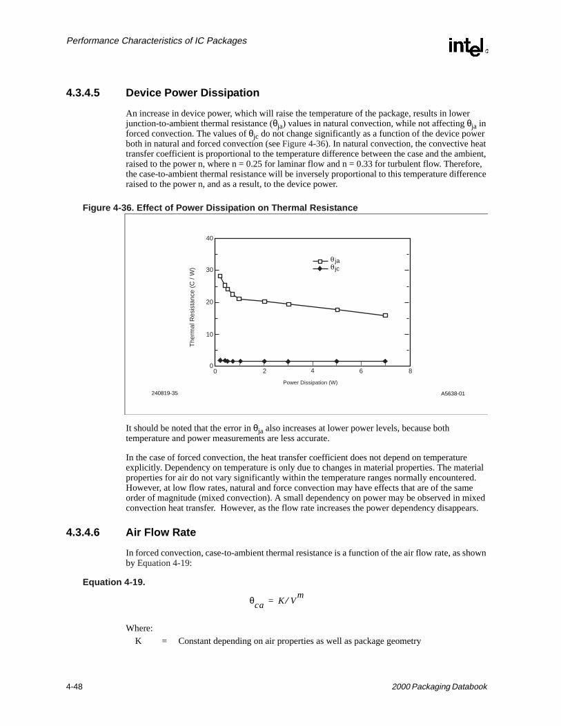
Performance Characteristics of IC Packages
4.3.4.5 Device Power Dissipation
An increase in device power, which will raise the temperature of the package, results in lower junction-to-ambient thermal resistance (θja) values in natural convection, while not affecting θja in forced convection. The values of θjc do not change significantly as a function of the device power both in natural and forced convection (see Figure 4-36). In natural convection, the convective heat transfer coefficient is proportional to the temperature difference between the case and the ambient, raised to the power n, where n = 0.25 for laminar flow and n = 0.33 for turbulent flow. Therefore, the case-to-ambient thermal resistance will be inversely proportional to this temperature difference raised to the power n, and as a result, to the device power.
Figure 4-36. Effect of Power Dissipation on Thermal Resistance
It should be noted that the error in θja also increases at lower power levels, because both temperature and power measurements are less accurate.
In the case of forced convection, the heat transfer coefficient does not depend on temperature explicitly. Dependency on temperature is only due to changes in material properties. The material properties for air do not vary significantly within the temperature ranges normally encountered. However, at low flow rates, natural and force convection may have effects that are of the same order of magnitude (mixed convection). A small dependency on power may be observed in mixed convection heat transfer. However, as the flow rate increases the power dependency disappears.
4.3.4.6 Air Flow Rate
In forced convection, case-to-ambient thermal resistance is a function of the air flow rate, as shown by Equation 4-19:
Equation 4-19.
Where:
A5638-01240819-35
The
rmal
Res
ista
nce
(C /
W)
20
30
40
10
00 2 4 6 8
jajc
Power Dissipation (W)
θca K Vm⁄=
K = Constant depending on air properties as well as package geometry
4-48 2000 Packaging Databook

Performance Characteristics of IC Packages
Figure 4-37 shows how θja varies as a function of air flow rate for 168-lead PGA with and without heat fins. At lower air flow rates, there is a strong dependency of θja on the air flow rate, but as the air flow rate increases, θja values become less sensitive to the changes in the flow rate.
Figure 4-37. Effect of Air Flow Rate on Thermal Resistance of 168-Lead PGA Package
4.3.5 Mounting Parameters
4.3.5.1 PC Board Size And Thermal Conductivity
The printed circuit board on to which components are mounted can act as a fin by virtue of its thermal conductivity. The effect of conduction in the printed circuit board is illustrated in Figure 4-38. The effect of the board size on overall thermal resistance may vary, depending on the thermal resistance between the junction and the board compared to the resistance between the case and the ambient. Smaller packages with a relatively high case-to-ambient thermal resistance value are more dependent on the board for transfer of heat to ambient than are the larger size packages. Consequently, board size will have a much larger impact on the junction-to-ambient thermal resistance for such packages.
Another factor that impacts the thermal resistance from board to ambient is board thermal conductivity. As board thermal conductivity or board thickness increases, the spreading resistance for lateral conduction of heat within the board decreases. As a result a larger board area becomes available for heat transfer to the ambient.
V = Air velocity (m/s)
m = 1/2 and 4/5 for laminar and turbulent flow respectively
θja θjc K Vm⁄+=
A5639-01240819-36
The
rmal
Res
ista
nce
(C /
W)
ja, Without Fin
Air Flow (LFM)
0 200 400 600 800 10000
5
10
15
20
ja, With Finjc, Without Finjc, With Fin
2000 Packaging Databook 4-49

Performance Characteristics of IC Packages
Figure 4-38. Effect of PC Board Material and Size on Thermal Resistance of 132-Lead PQFP
4.3.5.2 PC Board Temperature
The temperature of the printed circuit board may significantly impact package thermal resistance but is normally ignored in thermal packaging design. A board of specific size and material properties, with only the component under consideration mounted on it, will have a unique equilibrium temperature distribution under fixed environmental and mounting conditions. However, if there are other components on the board, or the board is attached to a heat sink, the maximum board temperature, Tb,may increase or decrease. A change in board temperature will affect the junction temperature and consequently the junction-to-ambient thermal resistance. The junction-to-ambient thermal resistance, θja, measured when the board is influenced by other heating or cooling factors, is referred to as the apparent thermal resistance or systems-level thermal resistance θja,s.
In almost all practical applications, printed circuit boards are populated by many components, and heating of one package influences the thermal performance of other packages. In order to get a relatively good estimate of system thermal resistance, θja,s and θja values must be correlated through another parameter. As it turns out, this parameter is Tb. A simple reistor network shown in Figure 4-39 can be used to obtain this correlation. In this model, it is assumed that the heat flows from the junction to the package boundary, and from there a portion of the heat is transferred directly to the ambient, while the rest goes into the board and is distributed and transferred to the ambient.
A5640-01240819-37
The
rmal
Res
ista
nce
(C /
W)
Junc
tion
- To
- A
mbi
ent
0
50
10 2040
60
K = 0.64 (w / m c)K = 2.2 (w / m c)
PC Board Area / Package Area
4-50 2000 Packaging Databook

Performance Characteristics of IC Packages
Figure 4-39. Simplified Resistor Network
It should be noted that the model shown in Figure 4-39 is simplified, and the actual package resistor network model can be more complex. The following expression shows the relation between θja,s and θja and board temperature rise (Tb - Ta):
Equation 4-20.
A5641-01240819-38
TJ
RC
RB
TB
BAR
TA
TA
CAR
RC
θja s, θja S+=Tb T–
P---------------
SRa
Ra Rb+--------------------=
SRaRbRa Rb Rba+ +( )
-----------------------------------------
where:
P = Power dissipation (W)
Ra = Case-to-ambient resistance (C/W)
Rb = Case-to-board resistance (C/W)
Rba = Board-to-ambient resistance (C/W)
Rc = Junction-to-case resistance (C/W)
S = Sensitivity parameter, Ra/(Ra + Rb) (O < S < 1)
Tb - Ta = Board temperature rise over ambient (C)
2000 Packaging Databook 4-51

Performance Characteristics of IC Packages
Equation 4-20 shows a linear dependence of θja,s on board temperature rise; as the board temperature increases or decreases, the system thermal resistance will increase or decrease. The rate of these changes is dictated by sensitivity parameter S, which in turn depends on Ra/Rb. As Ra/ Rb increases, thermal resistance becomes more sensitive to board temperature rise; in other words, the packages becomes more thermally coupled with other components on the board. Large values of Ra/Rb indicate that the package depends more on the board for transfer of heat to the ambient than on direct heat transfer to the ambient (larger packages vs. smaller packages). On the other hand, as Ra/Rb decreases, S decreases. Smaller Ra/Rb means a higher degree of insulation between the package and the board. For example, the thermal resistance of a package with a copper lead frame is more sensitive to board temperature rise than its counterpart with an Alloy 42 lead frame, as shown in Figure 4-40.
Figure 4-40. Effect of Board Temperature Rise on Thermal Resistance of 132-Lead PQFP with Copper and Alloy 42-Lead Frames
To determine sensitivity factors and intercept in expression 12, the package system thermal resistance can be measured under two different board temperature conditions (θja is assumed to be known).
4.3.5.3 System Thermal Design
As shown in Figure 4-41, the packaging of an electronic system starts with the design or selection of the structure that houses the silicon integrated circuit or chip, proceeds to the chip-to-chip interconnect, continues to the board-to-board level and concludes at the box or cabinet, which houses the complete system.
A5642-01240819-39
The
rmal
Res
ista
nce
(C /
W)
Junc
tion
- To
- A
mbi
ent
K = 0.64 (w / m c)K = 2.2 (w / m c)
0 20 40 60 80 1000
20
120
100
80
60
40
Board Temperature RiseAbove Ambient (C)
4-52 2000 Packaging Databook

Performance Characteristics of IC Packages
nected g. The
use ally. A
Figure 4-41. The Packaging Hierarchy
4.3.6 Typical Configuration of PCs
PC chassis are divided into two categories: desktops and notebooks. Desktops have two major categories: LPX (Low Profile) and Baby AT. A typical LPX PC is 17” x 16” X 4”. Figure 4-42 shows a general configuration. The add-in boards are inserted horizontally into the slots conto the mother board. There are two fans, one for the power supply and one for general coolintotal system power is usually around 100 Watts.
Figure 4-42. The Configuration of the LPX PCs
Figure 4-43 shows the configuration of the Baby AT PC. Its typical size is 20” x 17” x 6”. Becaof the larger available space, more add-in boards can be inserted into the mother board vertictypical system power is around 120 Watts.
A5643-01240819-56
Chip Package
Board
System
Air Flow
Mother Board
CPU
Fan
Add-InBoards
PowerSupply
HDD
FDD
Add-InBoards
A5644-01240819-57
Fan
2000 Packaging Databook 4-53

Performance Characteristics of IC Packages
U the d 12-
be in this
Figure 4-44 shows the configuration of a notebook with a typical size of 11” x 9” x 2”. The CPtypically consumes 4-8 Watts depending on the products used. Other components includingmother board, HDD, FDD and screen use about 6-10 Watts. The total system power is aroun15 Watts.
Figure 4-43. The Configuration of a Typical Baby AT PC
Figure 4-44. The Configuration of a Typical Notebook
4.3.6.1 Worst Case Design Methodology
For electronic systems to function properly under any circumstances, thermal designs must obtained under the worst case scenario. These worst case conditions are briefly discussed section.
Air Flow
Mother Board
CPU
Fan
Add-InBoards
PowerSupply
HDD
FDD
A5645-01240819-58
Fan
1 2 3 4
Air Flow
A5646-01240819-59
Mother Board
CPU Battery
Floppy DiskDrive
HardDiskDrive
Keyboard
4-54 2000 Packaging Databook

Performance Characteristics of IC Packages
the
ing a job. ent. e case, e to the rnal
ink-to-ion
e ailable
ss. olants
icient id
elow tly elp to drop in
he heat se of a less id g timized
CPU power: The use of the maximum CPU power is recommended for system thermal design purposes. The power dissipation values for the Intel family of processors are the maximum power levels for the corresponding processors.
Component power: The thermal impact of components such as the hard disk drive, video and memory cards, and PCMCIA must be taken into account for system level thermal design. In prototype testing, load boards with simulated components can be used to generate the maximum component heat dissipation to investigate the thermal performance of the system.
Ambient temperature: Although most electronic systems work at room temperatures (25 °C),thermal design must consider the extreme environments which the system may experience. Normally an ambient temperature of 35 °C to 40 °C is used by most system designers.
4.3.6.2 System Thermal Designs
As the total system level power dissipation increases and the system size decreases, designcost-effective thermal solution which satisfies all requirements is an increasingly challengingIn general, thermal management can be divided into internal and external thermal managemInternal thermal management handles the thermal resistance from the junction to the packagwhile the external thermal management handles the thermal resistance from the package casambient. For a general thermal system design problem, three factors namely Budgeting, InteThermal Management and External Thermal Management should be considered.
Budgeting: The total junction-to-ambient thermal resistance must be distributed among the various sections of the thermal path; from chip-to-package, package-to-heat-sink and heat-sinside-ambient and inside-ambient-to-outside ambient. The thermal resistance in each sectmust then be managed to meet the assigned thermal budget.
Internal thermal management: This involves selection of thermal interface materials, packagtype, bonding techniques, and via design. The design must also meet constraints of cost, avtechnologies, reliability, manufacturing processes, and yield.
External thermal management. This involves selection of the cooling mode (i.e. conduction, natural or forced convection, or radiation), heat sink design, and heat sink attachment proceFigure 4-45 shows the typical convective thermal resistance values obtained using various coand cooling modes.
When the component is cooled directly by contact with a gas or liquid, the resistance to the convective heat removal from the surface is inversely proportional to the product of the heattransfer coefficient and the wetted area, 1/(hA), where h is the convective heat transfer coeffand A is the wetted area. As shown in Figure 4-45, the convective coefficients range from 100 K/Wfor natural convection of air, to 33 K/W of forced air convection, to 1 K/W in flurochemical liquforced convection.
When direct cooling of the package surface is inadequate to maintain the chip temperature bdesired levels, a heat sink can be attached to the package. A heat sink provides a significanlarger wetted area for the heat transfer. In addition, the extended surfaces of the heat sink hspread the heat. However, the presence of the heat sink may increase the overall pressure the system, and the thermal interface between the package and the heat sink will introduce additional thermal conductive resistance. Proper management of the heat sink design and tsink attach method is required to achieve maximum thermal performance benefits from the uheat sink. Typical air-cooled heat sinks can reduce the external thermal resistance to valuesthan 15 K/W in natural convection and as low as 5 K/W for moderate forced convection. Liqucooled heat sinks can further reduce the external resistance to below 1 K/W. Once the coolinmode has been selected, heat sinks, fans, and the heat sink attachment process must be opfor the system level thermal solution.
2000 Packaging Databook 4-55

Performance Characteristics of IC Packages
Figure 4-45. Typical Convective Thermal Resistances for Various Coolants and Cooling Modes
4.3.6.2.1 Thermal Enhancement Options
There are many thermal enhancement options available to the package and system designer to reduce both the internal package thermal resistance as well as the package-to-ambient thermal resistance. Some of the commonly used enhancement techniques are summarized below.
Heat slug/spreader: In order for the heat to spread efficiently from the silicon die to the package, heat slugs or spreaders are used in the thermal design of many packages. The primary goal is to allow the heat to conduct from the die and spread into the heat spreader or slug. Since the heat transfer area provided by the slug is larger, it helps to reduce the thermal resistance. However, the use of heat slugs and spreaders present several design challenges; thermally induced stresses resulting from a mismatch between the coefficient of thermal expansion between the package and the heat slug or spreader, reliability of the attachment between the die and the slug, and manufacturability issues.
Thermal via and board design: Thermal vias are often used to reduce the thermal resistance of materials with low thermal conductivity like printed circuit boards or substrates. Via designs are divided into two configurations: stacked and staggered. In a stacked via design, successive via layers are stacked with vias on top of each other. In the staggered configuration, the vias are not stacked directly on top of vias in another layer.
Figure 4-46 shows an example of the stacked via designs on PCB. The via has an outside diameter D, height H and is plated with copper of thickness Tw. The thermal resistance of the n vias can be approximately estimated using one dimensional heat conduction analysis:
A5647-01240819-60
Air 1-3 atm
Fluorochemical Liquids
Air 1-3 atm
Fluorochemical Liquids
Water
WettedArea=10 cm2
ForcedConvection
NaturalConvection
0.01 0.1 1.0 10 100 1000
K/W
4-56 2000 Packaging Databook

Performance Characteristics of IC Packages
Equation 4-21.
where Rv is the total thermal resistance of the number (n) of vias and K is the thermal conductivity of the via plating material. Vias reduce the thermal resistance but increase the electrical routing difficulty. The density and size of the vias depends on many factors in the design criteria: electrical routing, thermal performance requirements, cost, etc. The final design is usually a trade-off among various considerations. For a fixed pitch to diameter (say, P/D = 2), the criterion favors vias with small diameters. However, when the pitch is fixed, the minimum thermal resistance is obtained with larger via diameters.
Figure 4-46. Via and Board Design
Heat sinks: Heat sinks vary in shape, size and material depending on applications. Figure 4-47 shows a regular cross cut pin fin heat sink and elliptical pin fin heat sink. The purpose of heat sinks is to spread the heat and to increase the heat transfer area wetted by the coolant. Although heat sinks help in heat spreading, the presence of the fins presents a blockage to the coolant flow causing an increase in the system level pressure drop. Increased pressure drop would require a larger fan to drive the required coolant flow through the computer chassis. The heat sink design (i.e. number, shape and size of fins) must be optimized in order to maximize the heat transfer from the heat sink with the smallest possible increase in the pressure drop.
Rv H Knπ⁄ DTw T2
w–( )=
A5648-01240819-62
H
Tw
DP
2000 Packaging Databook 4-57

Performance Characteristics of IC Packages
Figure 4-47. Square Pin and Elliptical Pin Heat Sinks
Metal plate or rod: Heat spreading should be considered in the thermal design of the system to minimize the temperature drop on the heat dissipating surfaces when: (1) concentrated heat must be transferred to places where space is available for more enhancements like heat sinks or fans, or simply where the thermal environment is more favorable; and (2) if a large surface area is required for heat dissipation. Table 4-17 compares the temperature drops at the ends of a 10" long 1" diameter rod with 1 Watt passing through the rod. Results show that the use of copper or aluminum decreases the thermal resistance by nearly two orders of over the typical PCB. In portable computer systems, flexible laminated copper foils called "flexible heat sinks" can be used in order to satisfy space and weight constraints.
Heat pipes: An increase in the cross-sectional area of a spreader plate made out of copper or aluminum can reduce the spreading thermal resistance. However, this approach is often constrained by the space and weight limitations of the system. Under such circumstances, heat pipes can be used for heat transfer. A typical heat pipe consists of a enclosed, partially evacuated chamber containing a small amount of liquid. The liquid evaporates in the heat pipe section in contact with a hot surface such as the processor package. The vapor travels to the colder sections of the heat pipe and condenses. The internal surface of the heat pipe consists of a mesh or sintered porous wick which transports the condensed liquid, via capillary fluid flow, to the hot section of the heat pipe. Thus, the heat pipe provides an enclosed, phase-change based system for transporting heat from hot to cold regions. Since heat removal in the hot section of the heat pipe, and condensation in the cold sections of the heat pipe involve phase change, there is almost no temperature gradient associated with transfering heat along the heat pipe. This is apparent from the temperature drop value for a heat pipe listed in Table 4-17. Heat pipe designs utilizing water, freons and dielectric fluorinert liquids are commercially available in a variety of configurations.
Fans: Fans provide forced air flow, which improves the convection coefficient significantly. Fans are widely used in desktop computers. However, their use in notebooks will require the resolution of issues typical of portables: power consumption (reducing battery life), space limitations, noise
A5649-01240819-64
Elliptical PinCross-CutSquare Pin
Table 4-17. Comparison of Spreading Efficiency of Different Rods
PCB Aluminum Copper Heat pipe
Temperature Drop (°C) 251 2.51 1.26 0.034
Thermal conductivity (W/m.K) 2 200 400 14800 (equivalent)
4-58 2000 Packaging Databook

Performance Characteristics of IC Packages
s it a very
TF ture
ystem, r has
hout
h
al used
he which ater to e test
nts from
test
voltage point nstant, to sed at 3
lation th
and reliability. In spite of these constraints, the use of fans in high performance notebooks is gaining acceptance because of the steady increase of CPU power and the fact that alternative non-fan solutions are becoming increasingly complicated and expensive.
Fan-sinks. Fans are most effective when combined with heat sinks. Fan-sinks have emerged to provide an integrated solution in improving the thermal performance while achieving smaller overall size and higher efficiency.
Active thermal feedback (ATF). The worst case design methodology often creates products that are “over-designed.” With the increasing complexity of thermal solutions, in many applicationmay not be economical to design products for the worst thermal case, which happens only tosmall portion of the products. Rather ATF can be implemented to deal with those extreme occasions. When the temperature of main components (say, CPU) reach certain threshold, Awill throttle the clock speed to reduce the power consumption of the system until the temperaof the system decreases to a safe level.
It should be noted that when developing a thermal management strategy for the electronic sit is no longer sufficient to focus only on temperature. Rather, the thermal/packaging engineeto understand, control and ultimately eliminate the thermally induced failures present througthe electronic system. The attainment of that goal, accompanied by the severe electrical, manufacturing, cost and reliability constraints, demands better collaboration of engineers witvarious backgrounds to better the design of the system so that it can provide all the desired functions reliably and inexpensively.
4.3.7 Design Methodology
Thermal packaging design at the component and system level may involve both experimentvalidation and modeling. The following sections describe the test methodology which can beto determine various package level thermal resistances.
4.3.7.1 Junction Temperature Measurements
In order to calculate thermal resistance values, the junction temperature is measured using ttemperature- sensitive parameter (TSP) method. This method employs special test structuresare the same size as the actual device. The test structure typically consists of a resistive hesimulate device power dissipation. The temperature sensors, located at different points on thstructure, may either be temperature sensitive diodes or resistors. Temperature measuremethese on-die temperature sensors are used to obtain an accurate estimate of the junction temperature.
A single package is mounted either directly or via a socket on a thermal test board. Differentboard designs , are used for surface mount and through-hole mount packages( see Figure 4-48 and Figure 4-49 respectively). The test chamber volume is 1ft3, and the ambient temperature is measured 12 inches away from the package (see Figure 4-50). In order to obtain accurate temperature measurements from the temperature sensing diodes/resistors, the diode outputor sensor resistance must first be correlated to the temperature. This is done using a three calibration technique. For calibration purposes, the test board assembly is immersed in a couniform temperature dielectric fluid bath The temperature of the dielectric fluid in the bath ismeasured using an RTD probe. The dielectric fluid in the bath is continuously stirred in ordermaintain temperature uniformity. If the temperature sensors are diodes, they are forward-biausing a 100 mA constant current source and the voltage drop accross the diode is measureddifferent bath temperatures. If the temperature sensors are resistors, a four wire resistance measurement is obtained at 3 different bath temperatures. A linear best fit straight line correis usually obtained to relate the diode voltage drop or sensor resistance to the measured batemperature
2000 Packaging Databook 4-59

Performance Characteristics of IC Packages
After calibration, the test structure is powered up to the desired power level. The on-die temperature sensors are continuously monitored until no change is detected in the temperature level, indicating an equilibrium state. At this stage, the chip surface temperatures, ambient and case temperatures, and device voltage drop and current are recorded. The device voltage drop and current are used to estimate the actual power dissipated in the test structure. When measuring thermal resistance under forced convection conditions, the test board assembly is exposed to a developed air flow. In this case, air velocity is measured at a location 12 inches upstream from the leading edge of the test board, using a hot wire anemometer. Air temperature is also measured at the same location.
4-60 2000 Packaging Databook

Performance Characteristics of IC Packages
Figure 4-48. Typical Thermal Test Board for Through Hole Mount Component
A5626-01
4.5 In.
6 In.
24019-25
2000 Packaging Databook 4-61

Performance Characteristics of IC Packages
Figure 4-49. Typical Thermal Test Board for Through Surface Mount Component
A5627-01
4.5 In.
5.5 In.
72 2
13284
240819-26
4-62 2000 Packaging Databook

Performance Characteristics of IC Packages
Figure 4-50. Test Chamber for Thermal Performance Testing
4.3.7.2 Case Temperature Measurement
Case temperature, "Tc", is measured at the center of the top surface of the package. This is typically the location with the highest temperature on the package case. Special care is required when measuring the case temperature to ensure an accurate temperature measurement. Usually, a thermocouple attached to the top surface of the package is used to measure Tc. Thermocouples must be calibrated before making temperature measurements. Moreover, different types of measurement errors are introduced when measuring the temperature of a surface which is at a temperature different from that of he surrounding ambient air. These errors could be caused due to poor thermal contact between the thermocouple junction and the package case, and due to heat loss by radiation or by conduction through the thermocouple leads. To minimize measurement errors, the following approach is recommended:
• Use 36 gauge or finer diameter, type K, T, or J thermocouples. Intel laboratory testing is performed using type K thermocouples made by Omega (part number: 5TC-TTK-36-36).
• Attach the thermocouple bead to the center of the package top surface using high thermal conductivity cements. The laboratory testing is performed by using Omega Bond (part number: OB-101).
• The thermocouple should be attached at a 90° angle as shown in Figure 4-51.
• If the case temperature is measured with a heat sink attached to the package, drill a hole (no larger than 0.15 inches) through the heat sink to route the thermocouple wire out Figure 4-51.
12 In.
Air FlowDirection
Hot WireAnemometer
Test Board
Thermocouple
A5628-01240819-27
2000 Packaging Databook 4-63
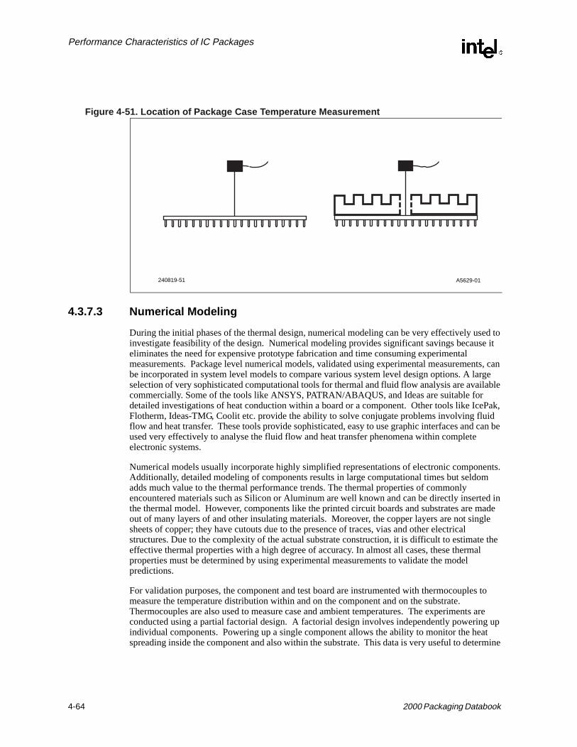
Performance Characteristics of IC Packages
Figure 4-51. Location of Package Case Temperature Measurement
4.3.7.3 Numerical Modeling
During the initial phases of the thermal design, numerical modeling can be very effectively used to investigate feasibility of the design. Numerical modeling provides significant savings because it eliminates the need for expensive prototype fabrication and time consuming experimental measurements. Package level numerical models, validated using experimental measurements, can be incorporated in system level models to compare various system level design options. A large selection of very sophisticated computational tools for thermal and fluid flow analysis are available commercially. Some of the tools like ANSYS, PATRAN/ABAQUS, and Ideas are suitable for detailed investigations of heat conduction within a board or a component. Other tools like IcePak, Flotherm, Ideas-TMG, Coolit etc. provide the ability to solve conjugate problems involving fluid flow and heat transfer. These tools provide sophisticated, easy to use graphic interfaces and can be used very effectively to analyse the fluid flow and heat transfer phenomena within complete electronic systems.
Numerical models usually incorporate highly simplified representations of electronic components. Additionally, detailed modeling of components results in large computational times but seldom adds much value to the thermal performance trends. The thermal properties of commonly encountered materials such as Silicon or Aluminum are well known and can be directly inserted in the thermal model. However, components like the printed circuit boards and substrates are made out of many layers of and other insulating materials. Moreover, the copper layers are not single sheets of copper; they have cutouts due to the presence of traces, vias and other electrical structures. Due to the complexity of the actual substrate construction, it is difficult to estimate the effective thermal properties with a high degree of accuracy. In almost all cases, these thermal properties must be determined by using experimental measurements to validate the model predictions.
For validation purposes, the component and test board are instrumented with thermocouples to measure the temperature distribution within and on the component and on the substrate. Thermocouples are also used to measure case and ambient temperatures. The experiments are conducted using a partial factorial design. A factorial design involves independently powering up individual components. Powering up a single component allows the ability to monitor the heat spreading inside the component and also within the substrate. This data is very useful to determine
A5629-01240819-51
4-64 2000 Packaging Databook

Performance Characteristics of IC Packages
the thermal properties for simplified component representations. Such experimental data can be used to determine the thermal properties which when used in the numerical model would provide temperature predictions to a reasonable degree of accuracy.
4.4 References
[1] Suhir E., "Calculated Thermally Induced Stresses in Adhesively Bonded and Soldered Assemblies", ISHM International Symposium on Microelectronics, Atlanta, Georgia, Oct 1986.
[2] "Guidelines for Accelerated Reliability Testing of Surface Mount Solder Attachments", IPC-SM-785, Nov 1992.
[3] Born, M., and Wolf, E., Principles of Optics, pp. 286-300, 1980, Pergamon Press, Oxford.
[4] Guo, Y., and Liu, S., "Development in Optical Methods for Reliability Analyses in Electronic Packaging Applications," Experimental/Numerical Mechanics in Electronic Packaging, vol. 2, pp. 10-21, R. Mahajan, B. Han, and D. Barker, ed., Society for Experi-mental Mechanics, Bellevue, WA, June 1997.
[5] Post, D., Han, B., and Ifju, P., High Sensitivity Moiré, 1994, Springer-Verlag, Inc., New York.
4.5 Revision Summary
• Re-wrote section 4.2
• Re-wrote several portions of section 4.3
• Added a section on numerical modeling
• General edit of all other sections
2000 Packaging Databook 4-65

Performance Characteristics of IC Packages
4-66 2000 Packaging Databook