AN 556: Using the Design Security Features in Intel … 556: Using the Design Security Features in...
40
AN 556: Using the Design Security Features in Intel FPGAs Subscribe Send Feedback AN-556 | 2017.12.18 Latest document on the web: PDF | HTML
Transcript of AN 556: Using the Design Security Features in Intel … 556: Using the Design Security Features in...

AN 556: Using the Design SecurityFeatures in Intel FPGAs
SubscribeSend Feedback
AN-556 | 2017.12.18Latest document on the web: PDF | HTML
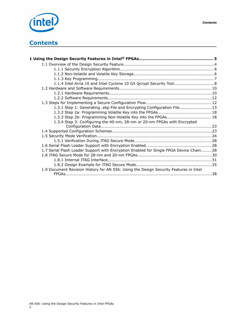
Contents
1 Using the Design Security Features in Intel® FPGAs........................................................ 31.1 Overview of the Design Security Feature....................................................................4
1.1.1 Security Encryption Algorithm...................................................................... 61.1.2 Non-Volatile and Volatile Key Storage............................................................ 61.1.3 Key Programming....................................................................................... 71.1.4 Intel Arria 10 and Intel Cyclone 10 GX Qcrypt Security Tool..............................8
1.2 Hardware and Software Requirements..................................................................... 101.2.1 Hardware Requirements.............................................................................101.2.2 Software Requirements..............................................................................12
1.3 Steps for Implementing a Secure Configuration Flow................................................. 121.3.1 Step 1: Generating .ekp File and Encrypting Configuration File........................ 131.3.2 Step 2a: Programming Volatile Key into the FPGAs........................................ 181.3.3 Step 2b: Programming Non-Volatile Key into the FPGAs................................. 181.3.4 Step 3: Configuring the 40-nm, 28-nm or 20-nm FPGAs with Encrypted
Configuration Data................................................................................... 231.4 Supported Configuration Schemes...........................................................................231.5 Security Mode Verification......................................................................................24
1.5.1 Verification During JTAG Secure Mode..........................................................281.6 Serial Flash Loader Support with Encryption Enabled................................................. 281.7 Serial Flash Loader Support with Encryption Enabled for Single FPGA Device Chain........281.8 JTAG Secure Mode for 28-nm and 20-nm FPGAs........................................................30
1.8.1 Internal JTAG Interface..............................................................................311.8.2 Design Example for JTAG Secure Mode.........................................................35
1.9 Document Revision History for AN 556: Using the Design Security Features in IntelFPGAs..............................................................................................................38
Contents
AN 556: Using the Design Security Features in Intel FPGAs2
1 Using the Design Security Features in Intel® FPGAsThis application note describes how you can use the design security features in Intel®40-, 28- and 20-nm FPGAs to protect your designs against unauthorized copying,reverse engineering, and tampering of your configuration files. This application noteprovides the hardware and software requirements for the 40-, 28- and 20-nm FPGAsdesign security features. This application note also provides steps for implementingsecure configuration flow.
Note: This application note uses the term "40-nm","28-nm" or "20-nm" FPGAs. The followingtable lists the supported FPGAs and its applicable devices.
Table 1. Supported FPGAs
FPGA Devices
40 nm Arria® II and Stratix® IV
28 nm Arria V, Cyclone® V, and Stratix V
20 nm Intel Arria 10 and Intel Cyclone 10 GX
In the commercial and military environments, design security is an importantconsideration for digital designers. As FPGAs start to play a role in larger and morecritical system components, it is important to protect the designs from unauthorizedcopying, reverse engineering, and tampering. Intel FPGAs address these concerns byencrypting their configuration bitstreams with the 256-bit Advanced EncryptionStandard (AES) algorithm.
Table 2. AES Modes in Supported Intel FPGAs
FPGA AES Mode
40 nm Counter Mode (CTR)
28 nm Cipher-block chaining (CBC)
20 nm CTR and keyed-hash message authentication code (HMAC)
During device operation, FPGAs store configuration data in SRAM configuration cells.Because SRAM memory is volatile, the SRAM cells must be loaded with configurationdata each time the device powers up. Configuration data is typically sent from anexternal memory source, such as a flash memory or a configuration device, to theFPGA. It is possible to intercept the configuration data when it is being sent from thememory source to the FPGA. If the configuration data were not encrypted, you coulduse the intercepted configuration data to configure another FPGA.
Intel FPGAs offer both volatile and non-volatile key storage. The key is stored in FPGAswhen using the design security feature. Depending on the security mode, you canconfigure the FPGAs with a configuration file that is encrypted with the same key, orfor board testing, configure with a normal configuration file.
AN-556 | 2017.12.18
Intel Corporation. All rights reserved. Intel, the Intel logo, Altera, Arria, Cyclone, Enpirion, MAX, Nios, Quartusand Stratix words and logos are trademarks of Intel Corporation or its subsidiaries in the U.S. and/or othercountries. Intel warrants performance of its FPGA and semiconductor products to current specifications inaccordance with Intel's standard warranty, but reserves the right to make changes to any products and servicesat any time without notice. Intel assumes no responsibility or liability arising out of the application or use of anyinformation, product, or service described herein except as expressly agreed to in writing by Intel. Intelcustomers are advised to obtain the latest version of device specifications before relying on any publishedinformation and before placing orders for products or services.*Other names and brands may be claimed as the property of others.
ISO9001:2008Registered

The design security feature is available when configuring the FPGAs with fast passiveparallel (FPP) configuration scheme with an external host (such as a MAX® II or MAX Vdevice or microprocessor) or when using active serial (AS) or passive serial (PS)configuration schemes.
Related Links
• Configuration, Design Security, and Remote System Upgrades in Arria II DevicesProvides more information about the design security for Arria II devices.
• Configuration, Design Security, and Remote System Upgrades in Stratix IV DevicesProvides more information about the design security for Stratix IV devices.
• Configuration, Design Security, and Remote System Upgrades in Arria V DevicesProvides more information about the design security for Arria V devices.
• Configuration, Design Security, and Remote System Upgrades in Cyclone VDevices
Provides more information about the design security for Cyclone V devices.
• Configuration, Design Security, and Remote System Upgrades in Stratix V DevicesProvides more information about the design security for Stratix V devices.
• Configuration, Design Security, and Remote System Upgrades in Arria 10 DevicesProvides more information about the design security for Arria 10 devices.
• Configuration, Design Security, and Remote System Upgrades in Intel Cyclone 10GX Devices
Provides more information about the design security for Intel Cyclone 10devices.
• Configuration Design Security in MAX 10 FPGA
1.1 Overview of the Design Security Feature
The design security feature for Intel FPGAs protects against unauthorized copying ,reverse engineering, and tampering. The following table lists some of the designapproaches to make the solution secure.
The 20-nm FPGAs have additional security features that you can enable by burning afuse, or by setting an option bit in the configuration bit-stream by using the stand-alone Qcrypt tool. Tamper-protection bit and JTAG Secure mode can be enabledseparately in 20-nm FPGAs only.
1 Using the Design Security Features in Intel® FPGAs
AN-556 | 2017.12.18
AN 556: Using the Design Security Features in Intel FPGAs4

Table 3. Design Security Approach for 40-nm and 28-nm FPGAs
Caution: Enabling the tamper-protection bit disables the test mode in 40-nm and 28-nm FPGAs.Disabling the test mode is irreversible and prevents Intel FPGA from carrying out failureanalysis. To enable the tamper protection bit, contact Intel FPGA Technical Support.
Design SecurityElement
40-nm FPGA 28-nm FPGA (1)
Non-Volatile key The non-volatile key is securely stored in fuses within the device. Proprietary security featuresmake it difficult to determine this key.
Volatile Key The volatile key is securely stored in battery-backed RAM within the device. Proprietary securityfeatures make it difficult to determine this key.
Key Generation Two user provided 256-bit strings areprocessed to generate a 256-bit key that isprogrammed into the device.
A user provided 256-bit key is processed by aone-way function before being programmedinto the device.
Key Choice User only set either 1 security key type (non-volatile key or volatile key) into the device.
Tamper ProtectionMode
Tamper protection mode prevents the FPGA from being loaded with an unencrypted configurationfile. When you enable this mode, the FPGA can only be loaded with a configuration that has beenencrypted with your key. Unencrypted configurations and configurations encrypted with the wrongkey will result in a configuration failure. You can enable this mode by setting a fuse within thedevice.
ConfigurationReadback
These devices do not support a configuration readback feature which makes readback of yourunencrypted configuration data infeasible.
Table 4. Design Security Approach for Intel Arria 10 and Intel Cyclone 10 GX FPGAs
Design SecurityElement
Description
Non-Volatile key The non-volatile key is securely stored in fuses within the device. Proprietary security featuresmake it difficult to determine this key.
Volatile Key The volatile key is securely stored in battery-backed RAM within the device. Proprietary securityfeatures make it difficult to determine this key.
Key Generation A user provided 256-bit key is processed by a one-way function before being programmed intothe device.
Key Choice Both volatile and non-volatile key can exist in a device. User can choose which key to use bysetting the option bits in encrypted configuration file through the Convert Programming File toolor the Qcrypt tool.
Tamper ProtectionMode
Tamper protection mode prevents the FPGA from being loaded with an unencrypted configurationfile. When you enable this mode, the FPGA can only be loaded with a configuration that has beenencrypted with your key. Unencrypted configurations and configurations encrypted with the wrongkey will result in a configuration failure. You can enable this mode by setting a fuse within thedevice.
continued...
(1) When you enable the tamper-protection bit in 28-nm FPGAs, the device will be in the JTAGsecure mode.
1 Using the Design Security Features in Intel® FPGAs
AN-556 | 2017.12.18
AN 556: Using the Design Security Features in Intel FPGAs5

Design SecurityElement
Description
ConfigurationReadback
These devices do not support a configuration readback feature. From a security perspective, thismakes readback of your unencrypted configuration data infeasible.
Security Key Control By using different JTAG instructions and the security option in the Qcrypt tool, you have theflexibility to permanently or temporarily disable the use of the non-volatile or volatile key. You canalso choose to lock the volatile key to prevent it from being overwritten or reprogrammed.
JTAG Access Control You can enable various levels of JTAG access control by setting the OTP fuses or option bits in theconfiguration file using the Qcrypt tool:1. Force full configuration or partial configuration to be done through HPS only.2. Bypass external JTAG pin or HPS JTAG. This feature disables external JTAG or HPS JTAG
access, but can be unlocked through internal core access. (2)
3. Disable all AES key related JTAG instructions from external JTAG pins.4. Allows only a limited set of mandatory JTAG instruction to be accessed through external JTAG,
similar to JTAG Secure mode.
Note: For additional details on these and other security features, contact Intel FPGATechnical Support.
Related Links
Intel Arria 10 and Intel Cyclone 10 GX Qcrypt Security Tool on page 8
1.1.1 Security Encryption Algorithm
Intel FPGAs have a dedicated AES decryptor block than can decrypt configuration bit-streams prior to configuring the FPGA device. The 28-nm FPGAs use the AES block inCBC mode, while the 40-nm and 20-nm FPGAs use the AES block in CTR mode. Inaddition, the 20nm devices implement techniques to mitigate side-channel attacksagainst the standard NIST CTR mode of encryption. If the security feature is not used,the AES decryptor is bypassed. The FPGAs AES implementation is validated asconforming to the Federal Information Processing Standards FIPS-197.
Related Links
• http://csrc.nist.gov/For the AES algorithm, refer to the Federal Information Processing StandardsPublication FIPS-197 or the AES Algorithm (Rijndael) Information .
• http://csrc.nist.gov/For the AES validation for FPGAs, refer to the Advanced Encryption StandardAlgorithm Validation List .
1.1.2 Non-Volatile and Volatile Key Storage
Intel FPGAs offer both volatile and non-volatile key storage. The volatile key storageregisters are reprogrammable and erasable. The contents of the key registers areretained between power-cycles with a coin-cell battery. Non-volatile key registers arefuse-based and are one-time programmable.
Note: Examples of lithium coin-cell type batteries that are used for volatile key storagepurposes are BR1220 (–30°C to 80°C) and BR2477A (–40°C to 125°C).
(2) Intel Cyclone 10 GX does not support force full configuration or partial configuration throughHPS and HPS JTAG Bypass.
1 Using the Design Security Features in Intel® FPGAs
AN-556 | 2017.12.18
AN 556: Using the Design Security Features in Intel FPGAs6
Table 5. Volatile and Non-Volatile Key Comparison
Option Volatile Key Non-Volatile Key
Key Length 256 bits 256 bits
Key Programmability Reprogrammable and erasable key One-time programmable key
External Battery Required Not required
Key Programming Method (3) On-board Both on-board and off-board (4)
Design Protection (5) Secure against copying, reverse engineering, and tampering (6)
Related Links
Intel FPGA Technical SupportTo enable tamper-protection bit.
1.1.3 Key Programming
Table 6. Key Programming Methods
Programming Procedure Method Programming Tool/Support
On-Board Programming Prototyping Intel FPGA Ethernet Cable (7), JTAG Technologies (8), Intel FPGA ParallelPort Cable (9), Intel FPGA Download Cable (10), and Intel FPGA DownloadCable II (11).
Production JTAG Technologies*
Off-Board Programming Prototyping System General*
Production System General*
(3) Key programming is carried out through JTAG interface. You need to use valid MSEL pinsettings for the JTAG interface.
(4) Programming the non-volatile key fuses uses the standard voltage sources used by the FPGAduring normal operation. No additional voltage rails are necessary for programming non-volatile key.
(5) Volatile key tamper-protection is only available for Arria II, Arria V, Cyclone V, Stratix V, IntelArria 10, and Intel Cyclone 10 GX devices.
(6) Tampering is prevented only when the volatile key tamper-protection bit is set, thuspreventing configuration with unencrypted Programmer Object Files (.pof).
(7) Intel FPGA Ethernet Cable supports both volatile and non-volatile key programming.
(8) JTAG Technologies* supports both volatile and non-volatile key programming.
(9) Intel FPGA Download Cable II supports only volatile key programming.
(10) Intel FPGA Download Cable support only volatile key programming except in 20-nm FPGAs,where it supports both volatile and non-volatile key programming.
(11) For non-volatile key programming, you must regulate the JTAG TCK pulse width (period) forproper polyfuse programming.
1 Using the Design Security Features in Intel® FPGAs
AN-556 | 2017.12.18
AN 556: Using the Design Security Features in Intel FPGAs7

Key programming uses the following definitions:
• On-board: procedure in which the device is programmed on your board
• Off-board: procedure in which the device is programmed on a separateprogramming system
• Prototyping: method initially used to verify proper operation of a particularmethod
• Production: method used for large-volume production
Related Links
Intel FPGA Technical SupportProvides information about programming support.
1.1.4 Intel Arria 10 and Intel Cyclone 10 GX Qcrypt Security Tool
The Qcrypt tool is a stand-alone encryption tool for encrypting and decrypting IntelArria 10 and Intel Cyclone 10 GX FPGA configuration bit-stream files. The Qcrypt toolcan also be used to encrypt HPS boot images through a script. Different kinds ofsecurity settings that are currently not accessible from the Intel Quartus® Primegraphical user interface can be set through the Qcrypt tool.
The Qcrypt tool encrypts and decrypts raw binary files (.rbf) only and not otherconfiguration files, such as .sof and .pof files. Throughout the encryption flow, theQcrypt tool will generate an authentication tag while encrypting the .rbf file. Theauthentication tag prevents any modification or tampering of the configuration bit-stream. Besides encryption and decryption, the Qcrypt tool allows you to enable andset various security features and settings. By incorporating security features andsettings into the .rbf file, you have the flexibility to use different kinds of securityfeatures on Intel Arria 10 and Intel Cyclone 10 GX devices without permanentlyburning the security fuses. To generate the .ekp file or encrypted configuration fileother than .rbf, you have to use the Intel Quartus Prime Convert Programming Filetool.
Note: The Qcrypt tool is not license-protected and can be used by all Intel Quartus Primesoftware user.
Related Links
• Qcrypt Tool Options on page 9Provides more information about Qcrypt tool features.
• AN 759: Arria 10 SoC Secure Boot User GuideProvides more information about encrypting HPS boot images.
• Overview of the Design Security Feature on page 4
1.1.4.1 Using Qcrypt Tool
You can use the following command to encrypt and decrypt .rbf files. This commandis the only way to set the advanced security options.
qcrypt [options] <input_file.rbf> <output_file.rbf>
1 Using the Design Security Features in Intel® FPGAs
AN-556 | 2017.12.18
AN 556: Using the Design Security Features in Intel FPGAs8
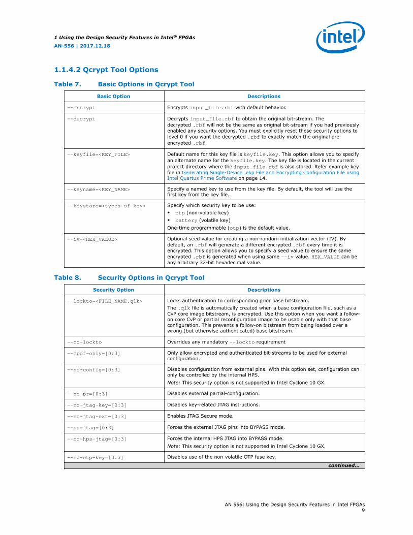
1.1.4.2 Qcrypt Tool Options
Table 7. Basic Options in Qcrypt Tool
Basic Option Descriptions
--encrypt Encrypts input_file.rbf with default behavior.
--decrypt Decrypts input_file.rbf to obtain the original bit-stream. Thedecrypted .rbf will not be the same as original bit-stream if you had previouslyenabled any security options. You must explicitly reset these security options tolevel 0 if you want the decrypted .rbf to exactly match the original pre-encrypted .rbf.
--keyfile=<KEY_FILE> Default name for this key file is keyfile.key. This option allows you to specifyan alternate name for the keyfile.key. The key file is located in the currentproject directory where the input_file.rbf is also stored. Refer example keyfile in Generating Single-Device .ekp File and Encrypting Configuration File usingIntel Quartus Prime Software on page 14.
--keyname=<KEY_NAME> Specify a named key to use from the key file. By default, the tool will use thefirst key from the key file.
--keystore=<types of key> Specify which security key to be use:• otp (non-volatile key)• battery (volatile key)One-time programmable (otp) is the default value.
--iv=<HEX_VALUE> Optional seed value for creating a non-random initialization vector (IV). Bydefault, an .rbf will generate a different encrypted .rbf every time it isencrypted. This option allows you to specify a seed value to ensure the sameencrypted .rbf is generated when using same --iv value. HEX_VALUE can beany arbitrary 32-bit hexadecimal value.
Table 8. Security Options in Qcrypt Tool
Security Option Descriptions
--lockto=<FILE_NAME.qlk> Locks authentication to corresponding prior base bitstream.The .qlk file is automatically created when a base configuration file, such as aCvP core image bitstream, is encrypted. Use this option when you want a follow-on core CvP or partial reconfiguration image to be usable only with that baseconfiguration. This prevents a follow-on bitstream from being loaded over awrong (but otherwise authenticated) base bitstream.
--no-lockto Overrides any mandatory --lockto requirement
--epof-only=[0:3] Only allow encrypted and authenticated bit-streams to be used for externalconfiguration.
--no-config=[0:3] Disables configuration from external pins. With this option set, configuration canonly be controlled by the internal HPS.Note: This security option is not supported in Intel Cyclone 10 GX.
--no-pr=[0:3] Disables external partial-configuration.
--no-jtag-key=[0:3] Disables key-related JTAG instructions.
--no-jtag-ext=[0:3] Enables JTAG Secure mode.
--no-jtag=[0:3] Forces the external JTAG pins into BYPASS mode.
--no-hps-jtag=[0:3] Forces the internal HPS JTAG into BYPASS mode.Note: This security option is not supported in Intel Cyclone 10 GX.
--no-otp-key=[0:3] Disables use of the non-volatile OTP fuse key.
continued...
1 Using the Design Security Features in Intel® FPGAs
AN-556 | 2017.12.18
AN 556: Using the Design Security Features in Intel FPGAs9
Security Option Descriptions
--no-battery-key=[0:3] Disables use of the battery-backed key.
--lock-battery-key=[0:3] Prevents the battery-backed volatile key from being changed or overwritten.
--secure=[2:3] Disables Test Mode <default=2>.
Related Links
• Intel Arria 10 and Intel Cyclone 10 GX Qcrypt Security Tool on page 8
• AN 759: Arria 10 SoC Secure Boot User GuideProvides more information about encrypting HPS boot images.
1.1.4.3 Security Levels of Qcrypt Tool Security Option
The Qcrypt tool allows the flexibility to determine the security level of the securityoptions in Table 8 on page 9. You can choose the minimum or maximum requirementby specifying the level of security from 0 to 3.
Table 9. Qcrypt Tool Security Option Security Levels
Security Level Descriptions
0 The security feature is not enabled unless by the corresponding OTP fuse.
1 The security feature is enabled from the start of the current full- or partial-reconfiguration until thestart of the next full configuration.
2 The security feature is enabled until the next power-on-reset. Additionally, configuration will notproceed if any action normally prevented by the security feature has taken place since the last power-on-reset.
3 Configuration will not proceed unless the security feature has been permanently enabled by blowingthe corresponding fuses in the device.
The security level of 2 provides a level of security almost as powerful as setting thecorresponding OTP security fuse, but with some flexibility. For example, the use ofJTAG may be required for manufacturing test or debug, but you may want to totallydisable JTAG while a secured (encrypted) bit-stream is loaded in the device.Furthermore, you may not want to load a secured bit-stream into a device that hadpreviously been probed with any kind of JTAG command.
Intel recommends that you use the strictest security level for each option that isconsistent with your design requirements.
Note: You can find information on the Qcrypt tool by using the --help option.
1.2 Hardware and Software Requirements
When using the design security feature, a volatile or non-volatile key is stored in theFPGA. The key must be programmed before the FPGA is configured with an encryptedconfiguration file.
1.2.1 Hardware Requirements
The following table lists the specifications that you must follow for a successful keyprogramming.
1 Using the Design Security Features in Intel® FPGAs
AN-556 | 2017.12.18
AN 556: Using the Design Security Features in Intel FPGAs10

Table 10. Specifications for Key Programming
Parameter Key Programming Mode
Non-Volatile Key Volatile Key
TCK period 10 µs ± 1 µs (12) —
Ambient Temperature 25°C ± 5°C 25°C ± 5°C
Voltage (VCCBAT) — (13)
VCCBAT is a dedicated power supply for the volatile key storage and is not shared withother on-chip power supplies, such as VCCIO or VCC. VCCBAT continuously suppliespower to the volatile register regardless of the on-chip supply condition.
Note: After power up, you must wait for the device to exit power-on reset (POR) beforebeginning the key programming. You may encounter verification error whenprogramming the volatile Encryption Key Programming (.ekp) file if you have theVCCBAT pin tied to GND. The VCCBAT pin must be tied to the recommended VCCBATvoltage provided in the repective device family pin connection guidelines for properoperation.
Related Links
• Device Datasheet for Arria II DevicesProvides more information about JTAG, POR, and voltage specifications.
• DC and Switching Characteristics for Stratix IV DevicesProvides more information about JTAG, POR, and voltage specifications.
• Arria V Device DatasheetProvides more information about JTAG, POR, and voltage specifications.
• Cyclone V Device DatasheetProvides more information about JTAG, POR, and voltage specifications.
• Stratix V Device DatasheetProvides more information about JTAG, POR, and voltage specifications.
• Intel Arria 10 Device DatasheetProvides more information about JTAG, POR, and voltage specifications.
• Intel Cyclone 10 GX Device DatasheetProvides more information about JTAG, POR, and voltage specifications.
• Stratix V E, GS, and GX Device Family Pin Connection Guidelines
• Stratix V GT Device Family Pin Connection Guidelines
• Arria V GT, GX, ST and SX Device Family Pin Connection Guidelines
• Arria V GZ Device Family Pin Connection Guidelines
• Stratix IV GX and E Device Family Pin Connection Guidelines
• Stratix IV GT Device Family Pin Connection Guidelines
• Arria II Device Family Pin Connection Guidelines
(12) Applies to 40-nm and 28-nm FPGAs only.
(13) If you do not use the volatile key, refer to the respective device family pin connectionguidelines for VCCBAT connection.
1 Using the Design Security Features in Intel® FPGAs
AN-556 | 2017.12.18
AN 556: Using the Design Security Features in Intel FPGAs11
• Intel Arria 10 GX, GT, and SX Device Family Pin Connection Guidelines
1.2.2 Software Requirements
Table 11. Supported Quartus Version for Intel FPGAsYou are required to use the supported Quartus software version below to enable the design security featurebased on your FPGA type.
Device Supported Quartus Version
40-nm FPGA Quartus II software version 9.0 or later.
28-nm FPGA Quartus II software version 11.0 or later.
20-nm FPGA Intel Quartus Prime software version 15.1 or later. (14)
Note: To enable the design security feature for Intel Quartus Prime Lite Edition, obtain alicense file from Intel FPGA Technical Support.
Related Links
Intel FPGA Technical Support
1.3 Steps for Implementing a Secure Configuration Flow
To implement a secure configuration flow, follow these steps:
1. Generate the .ekp file and encrypt the configuration data.
The Intel Quartus Prime configuration software always uses the user-defined 256-bit key to generate a key programming file and an encrypted configuration file.The encrypted configuration file is stored in an external memory, such as a flashmemory or a configuration device. For details, refer to Step 1: Generating .ekpFile and Encrypting Configuration File on page 13.
Note: For the 20-nm FPGAs, you can also encrypt an .rbf by using the stand-alone Qcrypt tool. The resulting encrypted .rbf can be added to a .pof fileby using the Intel Quartus Prime File:Generate Programming Filecommand.
2. Program the user-defined 256-bit key into the FPGAs.
For details, refer to Step 2a: Programming Volatile Key into the FPGAs on page18 and Step 2b: Programming Non-Volatile Key into the FPGAs on page 18.
3. Configure the 40-nm, 28-nm or 20-nm FPGA device.
At power up, the external memory source sends the encrypted configuration file tothe FPGA. The device uses the stored key to decrypt the file and to configureitself. For details about how to configure FPGAs with encrypted configuration data,refer to Step 3: Configuring the 40-nm, 28-nm or 20-nm FPGAs with EncryptedConfiguration Data on page 23.
(14) For 20-nm FPGAs, you can also enable the design security features by using the stand-aloneQcrypt tool available in the Intel Quartus Prime software.
1 Using the Design Security Features in Intel® FPGAs
AN-556 | 2017.12.18
AN 556: Using the Design Security Features in Intel FPGAs12

Figure 1. Secure Configuration Flow
AESDecryptor
FPGA
AES KEY
Encrypted Configuration
Data
Encryption KeyProgramming File
Encrypted Configuration
Data
ConfigurationData
Step 1. Generate the Encryption Key Programming File Encrypt Configuration Data and Store in External Memory
Intel Quartus Prime
Step 2. Program Key into DevicesEncryption Key Programming File
Volatile and Non-VolatileKey Storage
MemoryStorage
Encrypted
ConfigurationData
AESEncryptor
Step 3. Configure the Devices Using Encrypted Configuration Data
1.3.1 Step 1: Generating .ekp File and Encrypting Configuration File
To use the design security feature in the FPGAs, you must encrypt your 20-nm designusing the Qcrypt tool, or generate an .ekp file and encrypt your configuration filesusing the Intel Quartus Prime software. The key is not saved into any Intel QuartusPrime-generated configuration files and the actual 256-bit key is generated from thebit sequences.
To enable the design security feature, you can obtain a license file from Intel FPGATechnical Support.
The .ekp file has different formats, depending on the hardware and system used forprogramming. There are three file formats supported by the Intel Quartus Primesoftware:
• JAM Byte Code (.jbc) file
• JAM™ Standard Test and Programming Language (STAPL) Format (.jam) file
• Serial Vector Format (.svf) file
Only the .ekp file type is generated automatically from the Intel Quartus Primesoftware. You must create the .jam and .svf files using the Intel Quartus Primesoftware if these files are required in the key programming. The Intel Quartus Primesoftware generates the JBC format of the .ekp file in the same project directory.
Note: Intel recommends that you keep the .ekp file confidential.
Use the .ekp file with the Intel FPGA Ethernet Cable communications cable or IntelFPGA Download Cable download cable and the Intel Quartus Prime software. The IntelFPGA Ethernet Cable communications cable can support both volatile and non-volatilekey programming whereas the Intel FPGA Download Cable download cable is usedonly for volatile key programming. The .jam file format is generally used with third-party programming vendors and JTAG programmer vendors. The .svf file format isused with JTAG programmer vendors.
Related Links
Intel FPGA Technical SupportTo enable the design security feature, you must obtain a license file.
1 Using the Design Security Features in Intel® FPGAs
AN-556 | 2017.12.18
AN 556: Using the Design Security Features in Intel FPGAs13

1.3.1.1 Generating Single-Device .ekp File and Encrypting Configuration Fileusing Intel Quartus Prime Software
To generate a single device .ekp file and encrypt your configuration file, follow thesesteps:
1. Obtain a license file to enable the design security feature from Intel FPGATechnical Support.
2. Start the Intel Quartus Prime software.
3. On the Tools menu, click License Setup. The Options dialog box displays theLicense Setup options.
4. In the License file field, enter the location and name of the license file, or browseto and select the license file.
5. Click OK.
6. Compile your design with one of the following options:
a. On the Processing menu, click Start Compilation.
b. On the Processing menu, point to Start and click Start Assembler.
An unencrypted SRAM Object File (.sof) is generated.
7. On the File menu, click Convert Programming Files. The ConvertProgramming Files dialog box appears.
a. In the Convert Programming Files dialog box, select the programming filetype from the Programming file type list.
b. If applicable, select the appropriate configuration device from theConfiguration device list.
c. Select the mode from the Mode list.
d. Type the file name in the File name field, or browse to and select the file.
e. Under the Input files to convert section, click SOF Data.
f. Click Add File to open the Select Input File dialog box.
g. Browse to the unencrypted SOF file and click Open.
h. Under the Input files to convert section, click on the SOF file name. Thefield is highlighted.
i. Click Properties. The SOF Files Properties: Bitstream Encryption dialogbox appears.
j. In the SOF Files Properties: Bitstream Encryption dialog box, turn onGenerate encrypted bitstream.
k. Turn on Generate key programming file and type the .ekp file path and filename in the text area, or browse to and select <filename>.ekp.
l. Additional step for 20-nm FPGAs only: Turn on Enable volatile security keycheck box to encrypt the .sof file with volatile security key or turn it off touse non-volatile security key.
m. Additional step for 20-nm FPGAs only: Turn on Generate encryption lockfile and insert the .qlk file path and file name in the text area, or browse tothe desired <filename>.qlk.
1 Using the Design Security Features in Intel® FPGAs
AN-556 | 2017.12.18
AN 556: Using the Design Security Features in Intel FPGAs14

n. Add the keys to the pull-down list either with a .key file or the Add button.The Add and Edit buttons bring up the Key Entry dialog box. The Deletebutton deletes the currently selected key from the pull-down list.
Note: 40-nm FPGAs require entry of two 256-bit keys. The encyption derivedfrom a combination of the two 256-bit keys. 28-nm and 20-nm FPGAsrequire entry of a single 256-bit key. The final encryption key is derivedusing a one-way function.
Using the .key file option allows you to specify one or two key files in thecorresponding drop-down box. You may use different files for the Key 1 andKey 2 fields, or use one .key file for both.
The .key file is a plain text file in which each line represents a key unless theline starts with "#". The "#" symbol is used to denote comments. Each validkey line has the following format: <key identity><white space><256-bithexadecimal key>.
# This is an example key filekey1 0123456789ABCDEF0123456789ABCDEF0123456789ABCDEF0123456789ABCDEFkey2 ABCDEF0123456789ABCDEF0123456789ABCDEF0123456789ABCDEF0123456789
The key identity is an alphanumeric name that is used to identify the keys(similar to the key file entry). The key is also the text displayed when theShow entered keys button is turned off. It is displayed together with the fullkey when Show entered keys is turned on.
You can save the keys in the pull-down list to a .key file. You must click thecorresponding Save button to save a key and to display the standard Filedialog box. All keys in the pull-down list are saved to the selected orcreated .key file.
Select the Key Entry Method to enter the encryption key either with the on-screen keypad or keyboard.
The on-screen keypad allows you to enter the keys using the keypad. Select akey and click on the on-screen keypad to enter values. You have the option ofallowing the keys to be shown as they are entered. If you use this option, youdo not need to confirm the keys.
While the on-screen keypad is being used, any attempt to use the keyboard toenter the keys generates a pop-up notification and the key press is ignored.Alternatively, you can enter the encryption key from the keyboard.
i. Read the design security feature disclaimer. If you agree to andacknowledge the design security feature disclaimer, turn on theacknowledgment box.
ii. Click OK.
8. In the Convert Programming Files dialog box, click OK. The <filename>.ekpand encrypted configuration file are generated in the same project directory.
9. On the Tools menu, click Programmer. The Programmer dialog box appears.
10. In the Mode list, select JTAG as the programming mode.
11. Click Hardware Setup. The Hardware Setup dialog box appears.
a. In the currently selected hardware list, select Intel FPGA Ethernet Cable asthe programming hardware.
b. Click Done.
1 Using the Design Security Features in Intel® FPGAs
AN-556 | 2017.12.18
AN 556: Using the Design Security Features in Intel FPGAs15

12. Click Add File. The Select Programmer File dialog box appears.
a. Type <filename>.ekp in the File name field.
b. Click Open.
13. Highlight the .ekp file you added and click Program/Configure.
14. On the File menu, point to Create/Update and click Create JAM, SVF, or ISCFile. The Create JAM, SVF, or ISC File dialog box appears.
15. Select the file format required (JEDEC STAPL Format [.jam]), for the .ekp file inthe File format field.
16. Type the file name in the File name field, or browse to and select the file.
17. Click OK to generate the .jam file.
18. On the Tools menu, click Programmer Options. The Programmer Optionsdialog box appears.
Note: For non-volatile secure design feature, you must turn off the Configurevolatile design security key option to generate a non-volatile .svf file ofthe .ekp file.
19. Click OK.
20. Repeat 15 on page 16–17 on page 16 to generate a .svf file of the .ekp file. Usethe default setting in the Create JAM, SVF, or ISC File dialog box whengenerating a .svf file of the .ekp file.
1.3.1.2 Generating Single-Device .ekp File and Encrypting Configuration Fileusing Command-Line Interface in Intel Quartus Prime Software
There is a command-line interface that allows you to generate a single-device .ekp fileand encrypt Raw Binary File (.rbf). The command-line interfaces uses the IntelQuartus Prime software command-line executable, quartus_cpf, and requires thefollowing syntax or options:
• --key/-k <path to key file>:<key identity>
• A .sof file (user design)
• An .ekp file (the required encryption key programming file name)
You can create a compressed and uncompressed .rbf for configuration by using thefollowing command with an option file which contains the string compression=on.
quartus_cpf -c --option=<option file> --key<keyfile>:<keyid1>:<keyid2> <input_sof_file> <output_rbf_file>
Note: Encryption and compression cannot be used simultaneously in 20-nm FPGAs.
You can learn more on the option file from the Intel Quartus Prime software commandline help. Run quartus_cpf --help=option to learn more on the available options.For 20-nm FPGAs, use the Qcrypt tool command line to encrypt or decrypt the .rbffile. To generate the .ekp or encrypted configuration file other than .rbf, you haveto go through quartus_cpf.
Example 1.
The following example shows two sets of keys that are stored in two different keyfiles: key1 in key1.key and key2 in key2.key.
1 Using the Design Security Features in Intel® FPGAs
AN-556 | 2017.12.18
AN 556: Using the Design Security Features in Intel FPGAs16
quartus_cpf --key D: \SIV_DS\key1.key:key1 --key
D:\SIV_DS\key2.key:key2 D:\SIV_DS\test.sof D:\SIV_DS\test.ekp
Example 2.
The following example shows two sets of keys that are stored in the same key file:key1 and key2 in key12.key.
quartus_cpf --key
D:\SIV_DS\key12.key:key1:key2 D:\SIV_DS\test.sof D:\SIV_DS\test.ekp
1.3.1.3 Generating Multi-Device .ekp File and Encrypting Configuration File usingIntel Quartus Prime Software
To generate a multi-device .ekp file and encrypt your configuration file, follow thesesteps:
1. Start the Intel Quartus Prime software.
2. Repeat step 9 on page 15–step 11 on page 15 in Generating Single-Device .ekpFile and Encrypting Configuration File using Intel Quartus Prime Software on page14.
3. Click Add File. The Select Programmer File dialog box appears.
a. Select the single-device .ekp file, and type <single_ekp>.ekp in the Filename field.
b. Click Open.
Note: For the correct sequence of devices in the same JTAG chain, you can use theAuto-Detect option in the Intel Quartus Prime programmer. If one of theFPGA is not required to be key-programmed, you are not required to replacethe device with the <single_ekp>.ekp file in the Intel Quartus Primeprogrammer.
4. Repeat 3 on page 17 for each device in the same chain. Ensure the right devicesequence is used when adding the .ekp files to the programmer window.
5. Highlight all the .ekp files you added and click Program/Configure.
6. On the File menu, point to Create/Update and click Create JAM, SVF, or ISCFile. The Create JAM, SVF, or ISC File dialog box appears.
7. Select the required file format (.jam), for all the .ekp files in the File formatfield.
8. Type the file name in the File name field, or browse to and select the file.
9. Click OK to generate the .jam file.
10. On the Tools menu, click Programmer Options. The Programmer Optionsdialog box appears.
1 Using the Design Security Features in Intel® FPGAs
AN-556 | 2017.12.18
AN 556: Using the Design Security Features in Intel FPGAs17

Note: You must turn off Configure volatile design security key to generate anon-volatile .svf file of the .ekp file.
11. Click OK.
12. Repeat 7 on page 17–9 on page 17 to generate a .svf file for all the .ekp files.Use the default setting in the Create JAM, SVF, or ISC File dialog box whengenerating a .svf file of the .ekp file.
1.3.2 Step 2a: Programming Volatile Key into the FPGAs
Before programming the volatile key into the FPGAs, ensure that you can successfullyconfigure the FPGA with an unencrypted configuration file. The volatile key is areprogrammable and erasable key. Before you program the FPGAs with the volatilekey, you must provide an external battery to retain the volatile key. FPGAs with thevolatile key successfully programmed can accept both encrypted and unencryptedconfiguration bitstreams. This enables the use of unencrypted configuration bitstreamsfor board-level testing.
Any attempt to configure the FPGAs containing the volatile key with a configuration fileencrypted with the wrong key causes the configuration to fail. If this occurs, thenSTATUS signal from the FPGA pulses low and continues to reset itself if you enablethe Auto-restart configuration after error option in the Intel Quartus Primesoftware.
You can program the key into the FPGAs with on-board prototyping listed in KeyProgramming on page 7.
1.3.3 Step 2b: Programming Non-Volatile Key into the FPGAs
Before programming the non-volatile key into the devices, ensure that you cansuccessfully configure the FPGA with an unencrypted configuration file. Thenon-volatile key is one-time programmable through the JTAG interface. You canprogram the non-volatile key into the devices without an external battery. Deviceswith the non-volatile key successfully programmed can accept both encrypted andunencrypted configuration bitstreams. If you set the tamper protection bit, onlyencrypted configuration bitstreams are accepted. This enables the use of unencryptedconfiguration bitstreams for board-level testing.
Any attempt to configure the FPGAs containing the volatile key with a configuration fileencrypted with the wrong key causes the configuration to fail. If this occurs, thenSTATUS signal from the FPGA pulses low and continues to reset itself if you enablethe Auto-restart configuration after error option in the Intel Quartus Primesoftware.
You can program the non-volatile key into the devices using on-board prototyping,volume production, and off-board prototyping and production listed in KeyProgramming on page 7.
1 Using the Design Security Features in Intel® FPGAs
AN-556 | 2017.12.18
AN 556: Using the Design Security Features in Intel FPGAs18
1.3.3.1 Programming Volatile or Non-Volatile Key using Intel FPGA EthernetCable and Intel Quartus Prime Software
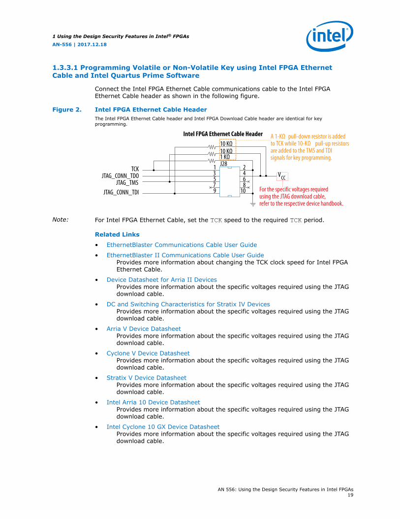
Connect the Intel FPGA Ethernet Cable communications cable to the Intel FPGAEthernet Cable header as shown in the following figure.
Figure 2. Intel FPGA Ethernet Cable HeaderThe Intel FPGA Ethernet Cable header and Intel FPGA Download Cable header are identical for keyprogramming.
Intel FPGA Ethernet Cable Header
J28 2468
10
1 35
79
1 KΩ
10 KΩ 10 KΩ
TCKJTAG_CONN_TDO
JTAG_TMSJTAG_CONN_TDI
VCC
For the specific voltages requiredusing the JTAG download cable,refer to the respective device handbook.
A 1-KΩ pull-down resistor is addedto TCK while 10-KΩ pull-up resistorsare added to the TMS and TDI signals for key programming.
Note: For Intel FPGA Ethernet Cable, set the TCK speed to the required TCK period.
Related Links
• EthernetBlaster Communications Cable User Guide
• EthernetBlaster II Communications Cable User GuideProvides more information about changing the TCK clock speed for Intel FPGAEthernet Cable.
• Device Datasheet for Arria II DevicesProvides more information about the specific voltages required using the JTAGdownload cable.
• DC and Switching Characteristics for Stratix IV DevicesProvides more information about the specific voltages required using the JTAGdownload cable.
• Arria V Device DatasheetProvides more information about the specific voltages required using the JTAGdownload cable.
• Cyclone V Device DatasheetProvides more information about the specific voltages required using the JTAGdownload cable.
• Stratix V Device DatasheetProvides more information about the specific voltages required using the JTAGdownload cable.
• Intel Arria 10 Device DatasheetProvides more information about the specific voltages required using the JTAGdownload cable.
• Intel Cyclone 10 GX Device DatasheetProvides more information about the specific voltages required using the JTAGdownload cable.
1 Using the Design Security Features in Intel® FPGAs
AN-556 | 2017.12.18
AN 556: Using the Design Security Features in Intel FPGAs19

1.3.3.2 Programming Single-Device Volatile or Non-Volatile Key using IntelQuartus Prime Software
To perform single-device volatile or non-volatile key programming using the IntelQuartus Prime software through the Intel FPGA Ethernet Cable, follow these steps:
1. Check the firmware version of the Intel FPGA Ethernet Cable. Verify that the JTAGfirmware build are up-to-date.
Note: Refer to the Cable and Adapter driver page to find the latest Intel FPGAEthernet Cable firmware build version.
2. Start the Intel Quartus Prime software.
3. On the Tools menu, click Programmer. The Programmer dialog box appears.
4. In the Mode list, select JTAG as the programming mode.
5. Click Hardware Setup. The Hardware Setup dialog box appears.
a. In the Currently selected hardware list, select Intel FPGA Ethernet Cableas the programming hardware.
b. Click Done.
6. Click Add File. The Select Programmer File dialog box appears.
a. Type <filename>.ekp in the File name field.
b. Click Open.
7. Highlight the .ekp file you added and click Program/Configure.
8. On the Tools menu, click Options. The Options dialog box appears.
9. In the Category list, click Programmer. You can choose to turn on or turn off theConfigure volatile design security key option to perform volatile or non-volatile key programming.
10. Click OK to close the Options dialog box.
11. Click Start to program the key.
Note: The Intel Quartus Prime software message window provides informationabout the success or failure of the key programming operation.
Related Links
EthernetBlaster Communications Cable User GuideProvides more information about JTAG firmware upgrade instructions.
1.3.3.3 Programming Single-Device Volatile or Non-Volatile Key using theCommand-Line Interface in Intel Quartus Prime Software
1 Using the Design Security Features in Intel® FPGAs
AN-556 | 2017.12.18
AN 556: Using the Design Security Features in Intel FPGAs20
To perform single-device volatile or non-volatile key programming using the IntelQuartus Prime software command-line interface through the Intel FPGA EthernetCable, follow these steps:
1. Perform step 1 on page 20 of Programming Single-Device Volatile or Non-VolatileKey using Intel Quartus Prime Software on page 20.
2. To determine the Intel FPGA Ethernet Cable cable port number that is connectedto the JTAG server, type quartus_jli -n at the command-line prompt.
3. With the single_ekp.jam file generated in Step 1: Generating .ekp File andEncrypting Configuration File on page 13, execute volatile or non-volatile keyprogramming to a single FPGA with the following command line:
• Volatile key programming:
quartus_jli -c<n> single_ekp.jam -aKEY_CONFIGURE
• Non-volatile key programming:
quartus_jli -c<n> single_ekp.jam -aKEY_PROGRAM
<n> is the port number returned with the -n option.
Note: The Intel Quartus Prime software command-line provides information aboutthe success or failure of the key programming operation.
Related Links
AN 425: Using the Command-Line Jam STAPL Solution for Device ProgrammingProvides more information about quartus_jli .
1.3.3.4 Programming Multi-Device Volatile or Non-Volatile Key using IntelQuartus Prime Software
To perform multi-device volatile or non-volatile key programming using the IntelQuartus Prime software through the Intel FPGA Ethernet Cable, follow these steps:
1. Repeat step 1 on page 20–step 5 on page 20 in Programming Single-DeviceVolatile or Non-Volatile Key using Intel Quartus Prime Software on page 20.
2. Click Add File. The Select Programmer File dialog box appears.
a. Programming using single-device .ekp files:
i. Type <single_device>.ekp in the File name field.
ii. Click Open.
iii. Repeat step 2.a.i on page 21–step 2.a.ii on page 21 for the number ofdevices in the same chain.
iv. Highlight the .ekp files you added and click Program/Configure.
Note: For the correct sequence of the devices in the same JTAG chain, you canuse the Auto-Detect option in the Intel Quartus Prime programmer.
b. Programming using a multi-device .jam file:
1 Using the Design Security Features in Intel® FPGAs
AN-556 | 2017.12.18
AN 556: Using the Design Security Features in Intel FPGAs21

i. Type <multi_device>.jam in the File name field.
ii. Click Open.
iii. Highlight the .jam file you added and click Program/Configure.
3. Repeat step 8 on page 20–step 10 on page 20 of Programming Single-DeviceVolatile or Non-Volatile Key using Intel Quartus Prime Software on page 20 toperform volatile or non-volatile key programming.
4. Click Start to program the key.
Note: The Intel Quartus Prime software message window provides informationabout the success or failure of the key programming operation.
1.3.3.5 Programming Multi-Device Volatile or Non-Volatile Key using theCommand-Line Interface in Intel Quartus Prime Software
To perform multi-device volatile or non-volatile key programming using the IntelQuartus Prime software command-line interface through the Intel FPGA EthernetCable, follow these steps:
1. Perform step 1 on page 20 of Programming Single-Device Volatile or Non-VolatileKey using Intel Quartus Prime Software on page 20.
2. To determine the Intel FPGA Ethernet Cable cable port number that is connectedto the JTAG server, type quartus_jli -n at the command-line prompt.
3. With the multi_ekp.jam file generated in Step 1: Generating .ekp File andEncrypting Configuration File on page 13, execute volatile or non-volatile keyprogramming for multiple FPGAs with the following command line:
• Volatile key programming:
quartus_jli -c<n> multi_ekp.jam -aKEY_CONFIGURE
• Non-volatile key programming:
quartus_jli -c<n> multi_ekp.jam -aKEY_PROGRAM
<n> is the port number returned with the -n option.
Note: The Intel Quartus Prime software command-line provides information aboutthe success or failure of the key programming operation.
1.3.3.6 Programming Key using JTAG Technologies
The key programming for your design is performed using a .svf file (.ekp file in .svfformat) and a JT 37xx boundary scan controller in combination with a JT2147QuadPod system.
Information about creating a .svf file to support multi-device programming isdescribed in Generating Multi-Device .ekp File and Encrypting Configuration File usingIntel Quartus Prime Software on page 17.
Related Links
JTAG TechnologiesProvides more information about procedures for JTAG programming.
1 Using the Design Security Features in Intel® FPGAs
AN-556 | 2017.12.18
AN 556: Using the Design Security Features in Intel FPGAs22
1.3.4 Step 3: Configuring the 40-nm, 28-nm or 20-nm FPGAs withEncrypted Configuration Data
The final step is to configure the protected 40-nm, 28-nm or 20-nm FPGAs with theencrypted configuration file.
During configuration, the encrypted configuration data is sent to the 40-nm, 28-nm or20-nm FPGAs. Using the previously stored key, the FPGA decrypts the configurationdata and uses the unencrypted data to configure itself. Only configuration filesencrypted using the correct key are accepted by the FPGA for successful configuration.Without a correct key, a stolen encrypted file is useless.
1.4 Supported Configuration Schemes
The design security feature is available in all configuration schemes exceptJTAG-based configuration.
Table 12. Design Security Support for Each Configuration Scheme
Configuration Scheme
Configuration Method DesignSecurity
Notes
FPP A MAX II or MAX V device, or amicroprocessor and a flash memory
Yes In this mode, the host system must send aDCLK signal that is 4x the data rate.
AS Serial configuration device Yes —
PS A MAX II or MAX V device, or amicroprocessor and a flash memory
Yes —
Download cable Yes The MicroBlaster™ tool is required toexecute encrypted PS configuration usinga .rbf through Intel FPGA Parallel Port Cableor ByteBlasterMV™ download cable.
JTAG Download cable — For volatile key programming only.
If your system contains a common flash interface (CFI) flash memory, you can alsouse it for the FPGA configuration. The MAX II and MAX V together with the Intel FPGAParallel Flash Loader (PFL) IP core provides an efficient method to program CFI flashmemory through the JTAG interface.
You can use the design security feature with other configuration features, such as thecompression and remote system upgrade features. When compression is used with thedesign security feature, the configuration file is first compressed and then encrypted inthe Intel Quartus Prime software. During configuration, the FPGA first decrypts andthen uncompresses the configuration file.
Note: Encryption and compression cannot be used simultaneously in 20-nm FPGAs.
You can either perform boundary-scan test (BST) or use the Signal Tap logic analyzerto analyze functional data within the FPGA. However, you cannot perform JTAGconfiguration after the key with tamper-protection bit set is programmed into the 40-nm, 28-nm or 20-nm FPGAs.
1 Using the Design Security Features in Intel® FPGAs
AN-556 | 2017.12.18
AN 556: Using the Design Security Features in Intel FPGAs23

When using the Signal Tap logic analyzer, you must first configure the device with anencrypted configuration file using PS, FPP, or AS configuration schemes. The designmust contain at least one instance of the Signal Tap logic analyzer. After the FPGA isconfigured with a Signal Tap logic analyzer instance in the design. Open the Signal Taplogic analyzer window in the Intel Quartus Prime software and click Scan Chain. Oncethe scanning is complete, the Signal Tap logic analyzer is ready to acquire data usingJTAG interface.
Related Links
• Configuration, Design Security, and Remote System Upgrades in Arria II DevicesProvides more information about the design security for Arria II devices.
• Configuration, Design Security, and Remote System Upgrades in Stratix IV DevicesProvides more information about the design security for Stratix IV devices.
• Configuration, Design Security, and Remote System Upgrades in Arria V DevicesProvides more information about the design security for Arria V devices.
• Configuration, Design Security, and Remote System Upgrades in Cyclone VDevices
Provides more information about the design security for Cyclone V devices.
• Configuration, Design Security, and Remote System Upgrades in Stratix V DevicesProvides more information about the design security for Stratix V devices.
• Configuration, Design Security, and Remote System Upgrades in Arria 10 DevicesProvides more information about the design security for Arria 10 devices.
• Configuration, Design Security, and Remote System Upgrades in Intel Cyclone 10GX Devices
Provides more information about the design security for Intel Cyclone 10devices.
1.5 Security Mode Verification
Intel FPGAs support the KEY_VERIFY JTAG instruction that allows you to verify theexisting security mode of the device. To check if you have successfully programmedthe volatile key, use the .jam files to automate the security mode verification steps.
Table 13. KEY_VERIFY JTAG Instruction
JTAG Instruction Instruction Code Description
KEY_VERIFY 00 0001 0011 Connects the key verification scanregister between TDI and TDO.
The KEY_VERIFY JTAG instruction allows you to read out the information on thesecurity features that are enabled on the chip. This instruction scans out associated bitvalues.
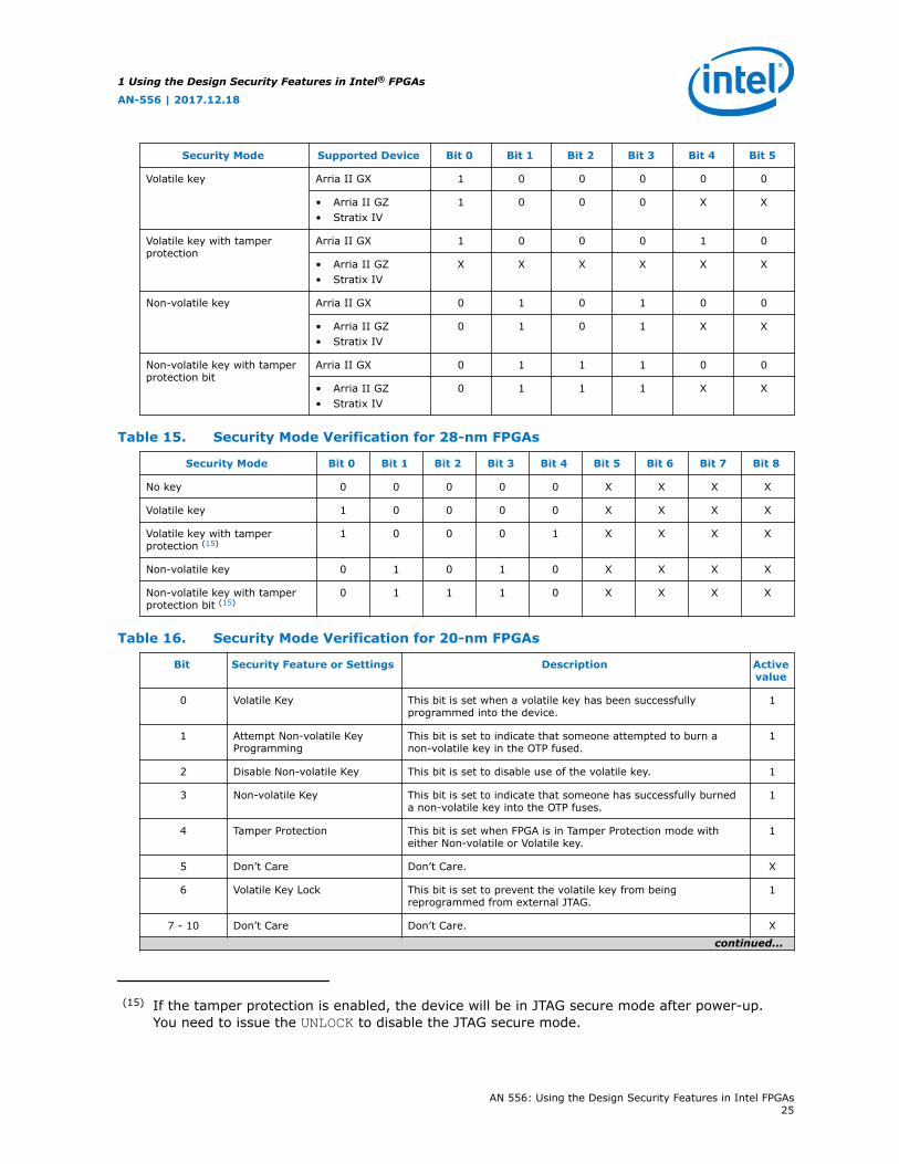
Table 14. Security Mode Verification for 40-nm FPGAs
Security Mode Supported Device Bit 0 Bit 1 Bit 2 Bit 3 Bit 4 Bit 5
No key Arria II GX 0 0 0 0 0 0
• Arria II GZ• Stratix IV
0 0 0 0 X X
continued...
1 Using the Design Security Features in Intel® FPGAs
AN-556 | 2017.12.18
AN 556: Using the Design Security Features in Intel FPGAs24
Security Mode Supported Device Bit 0 Bit 1 Bit 2 Bit 3 Bit 4 Bit 5
Volatile key Arria II GX 1 0 0 0 0 0
• Arria II GZ• Stratix IV
1 0 0 0 X X
Volatile key with tamperprotection
Arria II GX 1 0 0 0 1 0
• Arria II GZ• Stratix IV
X X X X X X
Non-volatile key Arria II GX 0 1 0 1 0 0
• Arria II GZ• Stratix IV
0 1 0 1 X X
Non-volatile key with tamperprotection bit
Arria II GX 0 1 1 1 0 0
• Arria II GZ• Stratix IV
0 1 1 1 X X
Table 15. Security Mode Verification for 28-nm FPGAs
Security Mode Bit 0 Bit 1 Bit 2 Bit 3 Bit 4 Bit 5 Bit 6 Bit 7 Bit 8
No key 0 0 0 0 0 X X X X
Volatile key 1 0 0 0 0 X X X X
Volatile key with tamperprotection (15)
1 0 0 0 1 X X X X
Non-volatile key 0 1 0 1 0 X X X X
Non-volatile key with tamperprotection bit (15)
0 1 1 1 0 X X X X
Table 16. Security Mode Verification for 20-nm FPGAs
Bit Security Feature or Settings Description Activevalue
0 Volatile Key This bit is set when a volatile key has been successfullyprogrammed into the device.
1
1 Attempt Non-volatile KeyProgramming
This bit is set to indicate that someone attempted to burn anon-volatile key in the OTP fused.
1
2 Disable Non-volatile Key This bit is set to disable use of the volatile key. 1
3 Non-volatile Key This bit is set to indicate that someone has successfully burneda non-volatile key into the OTP fuses.
1
4 Tamper Protection This bit is set when FPGA is in Tamper Protection mode witheither Non-volatile or Volatile key.
1
5 Don’t Care Don’t Care. X
6 Volatile Key Lock This bit is set to prevent the volatile key from beingreprogrammed from external JTAG.
1
7 - 10 Don’t Care Don’t Care. X
continued...
(15) If the tamper protection is enabled, the device will be in JTAG secure mode after power-up.You need to issue the UNLOCK to disable the JTAG secure mode.
1 Using the Design Security Features in Intel® FPGAs
AN-556 | 2017.12.18
AN 556: Using the Design Security Features in Intel FPGAs25

Bit Security Feature or Settings Description Activevalue
11 (16) Force Configuration from HPSonly
This bit is set when configuration is allowed from HPS only. 1
12 External JTAG Bypass This bit is set to indicate that external JTAG is disabled. 1
13 (17) HPS JTAG Bypass This bit is set to indicate that HPS JTAG is disabled. 1
14 (18) Disable Partial Reconfigurationand Scrubbing
This bit is set to indicate that external PR and externalscrubbing (including HPS PR and HPS scrubbing) are disabled.
1
15 Disable Volatile Key This bit is set to indicate that the volatile key is disabled. 1
16 Don’t Care Don’t Care. X
17 Disable Key Related JTAGInstructions
This bit is set to indicate that external JTAG access to all key-related JTAG instructions is disabled.
1
18 JTAG Secure Mode This bit is set to indicate that only mandatory JTAG instructionsare allowed to be externally accessed.
1
19 Don’t Care Don’t Care. X
20 Volatile Key Clear This bit is set when the volatile key is successfully cleared fromthe device.
1
The following examples show the .jam files to verify the FPGAs security modes.
Example 3. JAM File for 40-nm FPGAs (Arria II GX Devices)
STATE RESET;
STATE IDLE;
'Security Mode Identification
BOOLEAN verify_reg[6];
IRSCAN 10, $013;
WAIT 100 USEC;
DRSCAN 6, $0, CAPTURE verify_reg[5..0];
Example 4. JAM File for 40-nm FPGAs (Arria II GZ and Stratix IV Devices)
STATE RESET;
STATE IDLE;
'Key Verification
(16) Bit 11 is not applicable to Intel Cyclone 10 GX devices. In Intel Cyclone 10 GX devices, this bitis in a "don't care" condition.
(17) Bit 13 is not applicable to Intel Cyclone 10 GX devices. In Intel Cyclone 10 GX devices, this bitis in a "don't care" condition.
(18) Bit 14 is not applicable to Intel Cyclone 10 GX devices. In Intel Cyclone 10 GX devices, this bitis in a "don't care" condition.
1 Using the Design Security Features in Intel® FPGAs
AN-556 | 2017.12.18
AN 556: Using the Design Security Features in Intel FPGAs26

BOOLEAN verify_reg[4];
IRSCAN 10, $013;
WAIT 100 USEC;
DRSCAN 4, $0, CAPTURE verify_reg[3..0];
Example 5. JAM File for 28-nm FPGAs
STATE RESET;
STATE IDLE;
'Key Verification in JAM format
BOOLEAN verify_reg[9];
IRSCAN 10, $013;
WAIT 100 USEC;
DRSCAN 9, $0, CAPTURE verify_reg[8..0];
Example 6. JAM File for 20-nm FPGAs
STATE RESET;
STATE IDLE;
'Key Verification in JAM format
BOOLEAN verify_reg[21];
IRSCAN 10, $013;
WAIT 100 USEC;
DRSCAN 21, $0, CAPTURE verify_reg[20..0];
Related Links
• Configuration, Design Security, and Remote System Upgrades in Arria II DevicesProvides more information about the design security for Arria II devices.
• Configuration, Design Security, and Remote System Upgrades in Stratix IV DevicesProvides more information about the design security for Stratix IV devices.
• Configuration, Design Security, and Remote System Upgrades in Arria V DevicesProvides more information about the design security for Arria V devices.
• Configuration, Design Security, and Remote System Upgrades in Cyclone VDevices
Provides more information about the design security for Cyclone V devices.
• Configuration, Design Security, and Remote System Upgrades in Stratix V DevicesProvides more information about the design security for Stratix V devices.
• Configuration, Design Security, and Remote System Upgrades in Arria 10 DevicesProvides more information about the design security for Arria 10 devices.
1 Using the Design Security Features in Intel® FPGAs
AN-556 | 2017.12.18
AN 556: Using the Design Security Features in Intel FPGAs27

• Configuration, Design Security, and Remote System Upgrades in Intel Cyclone 10GX Devices
Provides more information about the design security for Intel Cyclone 10devices.
1.5.1 Verification During JTAG Secure Mode
Non-mandatory JTAG instructions are disabled when the tamper protection bit isenabled in 28-nm FPGAs. When executing KEY_VERIFY during the tamper protectionbit is programmed, TDI points to the BYPASS register. Due to this, executing theKEY_VERIFY instruction when the tamper protection bit has been set will result in0x0 (hex) being returned.
To check if the tamper protection bit has been programmed in a device, shift a userdefined pattern in when executing the KEY_VERIFY instruction and check that theTDO pattern received has a 0 shifted in.
In 20-nm FPGAs, KEY_VERIFY instruction can be executed during JTAG Secure mode.To perform verification during JTAG secure mode for 20-nm FPGAs, you can expect0x0 (hex) value being returned when executing USERCODE instruction.
Example 7. Verification During JTAG Secure Mode ExampleShift in 0x15A (1 0101 1010 in binary). If the tamper protection bit has beenprogrammed, since KEY_VERIFY=BYPASS, you should expect 0 1011 0100 wherethe last 0 is the content of the BYPASS register.
1.6 Serial Flash Loader Support with Encryption Enabled
Intel provides an in-system programming (ISP) solution for serial configurationdevices: the Intel FPGA Serial Flash Loader (SFL) IP core. You can instantiate the SFLblock in your design to provide the flexibility to update the design stored in the serialconfiguration device without reprogramming the configuration device through the ASinterface.
As long as the JTAG interface of the FPGA is accessible, you can use the SFL solutionfor your application. If the design security feature with tamper-protection bit is set,the SFL solution does not work. Although the JTAG programming is not supportedwhen the tamper-protection bit is set, you may instantiate the Intel FPGA SFL IP corein your design and execute the SFL programming for the first time before non-volatilekey programming with the tamper-protection bit is set in the FPGA.
1.7 Serial Flash Loader Support with Encryption Enabled for SingleFPGA Device Chain
To use the SFL IP core with the encryption feature enabled in a single FPGA devicechain, follow these steps:
1. Start the Intel Quartus Prime software.
2. Instantiate the SFL IP core in your FPGA top-level design.
3. Compile your design with one of the following options. An unencrypted .sof isgenerated.
1 Using the Design Security Features in Intel® FPGAs
AN-556 | 2017.12.18
AN 556: Using the Design Security Features in Intel FPGAs28

a. On the Processing menu, click Start Compilation; or
b. On the Processing menu, point Start and click Start Assembler.
4. Follow these steps to convert a .sof to a .jic file:
a. On the File menu, choose Convert Programming Files.
b. In the Convert Programming Files dialog box, scroll to the JTAG IndirectConfiguration File (.jic) from the Programming file type field.
c. In the Configuration device field, specify the serial configuration device.
d. In the File name field, browse to the target directory and specify an outputfile name.
e. Highlight the .sof data in the Input files to convert section.
f. Click Add File.
g. Select the .sof file that you want to convert to a .jic file.
h. Click OK.
i. Click on the .sof file name to encrypt the .sof file.
Note: To encrypt the .sof file, refer to step 7 on page 14 of Generating Single-Device .ekp File and Encrypting Configuration File using Intel QuartusPrime Software on page 14.
j. Highlight Flash Loader and click Add Device.
k. Click OK. The Select Devices page appears.
l. Select the target FPGA that you are using to program the serial configurationdevice.
m. Click OK.
5. Program the serial configuration device with the encrypted .jic file.
6. Program the key into the FPGA device.
Note: To program the key to a single FPGA device, follow the steps in Programming Single-Device Volatile or Non-Volatile Key using Intel QuartusPrime Software on page 20.
7. The encrypted FPGA is then configured by the programmed serial configurationdevice.
Note: To program the key with a .jam file, you must convert the .jic file to a .jamfile.
Related Links
• Using the Serial FlashLoader with the Quartus II Software
• Device Datasheet for Arria II DevicesProvides more information about the timing parameters for PS and FPPconfiguration schemes.
• DC and Switching Characteristics for Stratix IV DevicesProvides more information about the timing parameters for PS and FPPconfiguration schemes.
• Arria V Device DatasheetProvides more information about the timing parameters for PS and FPPconfiguration schemes.
1 Using the Design Security Features in Intel® FPGAs
AN-556 | 2017.12.18
AN 556: Using the Design Security Features in Intel FPGAs29

• Cyclone V Device DatasheetProvides more information about the timing parameters for PS and FPPconfiguration schemes.
• Stratix V Device DatasheetProvides more information about the timing parameters for PS and FPPconfiguration schemes.
• Intel Arria 10 Device DatasheetProvides more information about the timing parameters for PS and FPPconfiguration schemes.
• Intel Cyclone 10 GX Device DatasheetProvides more information about the timing parameters for PS and FPPconfiguration schemes.
1.8 JTAG Secure Mode for 28-nm and 20-nm FPGAs
FPGAs will be in JTAG Secure mode upon power up when you:
• Enable the tamper-protection bit for 28-nm FPGAs
• Enable the JTAG Secure settings for 20-nm FPGAs
Attention: 20-nm FPGAs do not support LOCK and UNLOCK JTAG instructions, you will not be ableto unlock external JTAG to access non-mandatory JTAG instructions.
During JTAG secure mode, many JTAG instructions are disabled. The 28-nm and 20-nm FPGAs in JTAG secure mode only allow you to exercise mandatory IEEE Std.1149.1 and IEEE Std. 1149.6 BST JTAG instructions. If you attempt to exercise a non-mandatory JTAG instruction when the FPGA is in the JTAG secure mode, the BYPASSJTAG instruction chain is selected and the instruction is not executed.
Table 17. Mandatory and Non-Mandatory IEEE Std. 1149.1 and IEEE Std. 1149.6 BSTJTAG Instructions
Mandatory IEEE Std. 1149.1 and IEEE Std. 1149.6 BSTJTAG Instructions
Non-Mandatory IEEE Std. 1149.1 and IEEE Std. 1149.6BST JTAG Instructions
• BYPASS
• EXTEST
• IDCODE
• LOCK
• UNLOCK
• SAMPLE/PRELOAD
• SHIFT_EDERROR_REG
• CONFIG_IO
• CLAMP
• EXTEST_PULSE (19)
• EXTEST_TRAIN (19)
• HIGHZ
• KEY_CLR_VREG
• KEY_VERIFY (19)
• PULSE_NCONFIG
• USERCODE
For 28-nm FPGAs, to enable the access of non-mandatory JTAG instructions, you mustissue the UNLOCK JTAG instruction to deactivate the JTAG secure mode. You can issuethe LOCK instruction to put the device back into JTAG secure mode. You can only issueboth the LOCK and UNLOCK JTAG instructions during user mode using internal JTAGinterface. Issuing these two instructions using the external JTAG pins does not activateor deactivate the JTAG secure mode.
(19) You can execute these JTAG instructions during JTAG Secure mode for 20-nm FPGAs.
1 Using the Design Security Features in Intel® FPGAs
AN-556 | 2017.12.18
AN 556: Using the Design Security Features in Intel FPGAs30

The LOCK and UNLOCK JTAG instructions only activate or deactivate the JTAG securemode on an FPGA with tamper-protection bit enabled. Issuing these two instructionson a device that has a tamper-protection bit disabled does not turn on or turn off theJTAG secure mode.
1.8.1 Internal JTAG Interface
There are two interfaces to access the JTAG control block in 28-nm and 20-nm FPGAs:the external JTAG interface and the internal JTAG interface.
The external JTAG interface accesses the JTAG control block through the physical JTAGpins—TCK, TDI, TDO, and TMS. You use the external JTAG interface for FPGAconfiguration when using JTAG configuration scheme via programming cables orexecuting JTAG instructions using external player or processor such as JAM player orJTAG chain debugger tool. The internal JTAG interface refers to the connectionbetween TCK, TDI, TDO, and TMS signals from the internal FPGA core fabric and theJTAG control block.
You can only access the JTAG control block using either one of these interfaces one ata time. For example, when you use the internal JTAG interface, the external JTAGinterface to the JTAG control block is disabled. To access the internal JTAG interface,you must include the WYSIWYG atom in your Intel Quartus Prime design.
Figure 3. Internal and External JTAG Interface Connection
JTAGControl Block
TDI
TMS
TCK
TDO
Core InterfaceInternal JTAG
TDICORE
TMSCORE
TCKCORE
TDOCORE
CORECTL
I/O InterfaceExternal JTAG
TDITMSTCKTDO
TDITMSTCKTDO
1 Using the Design Security Features in Intel® FPGAs
AN-556 | 2017.12.18
AN 556: Using the Design Security Features in Intel FPGAs31
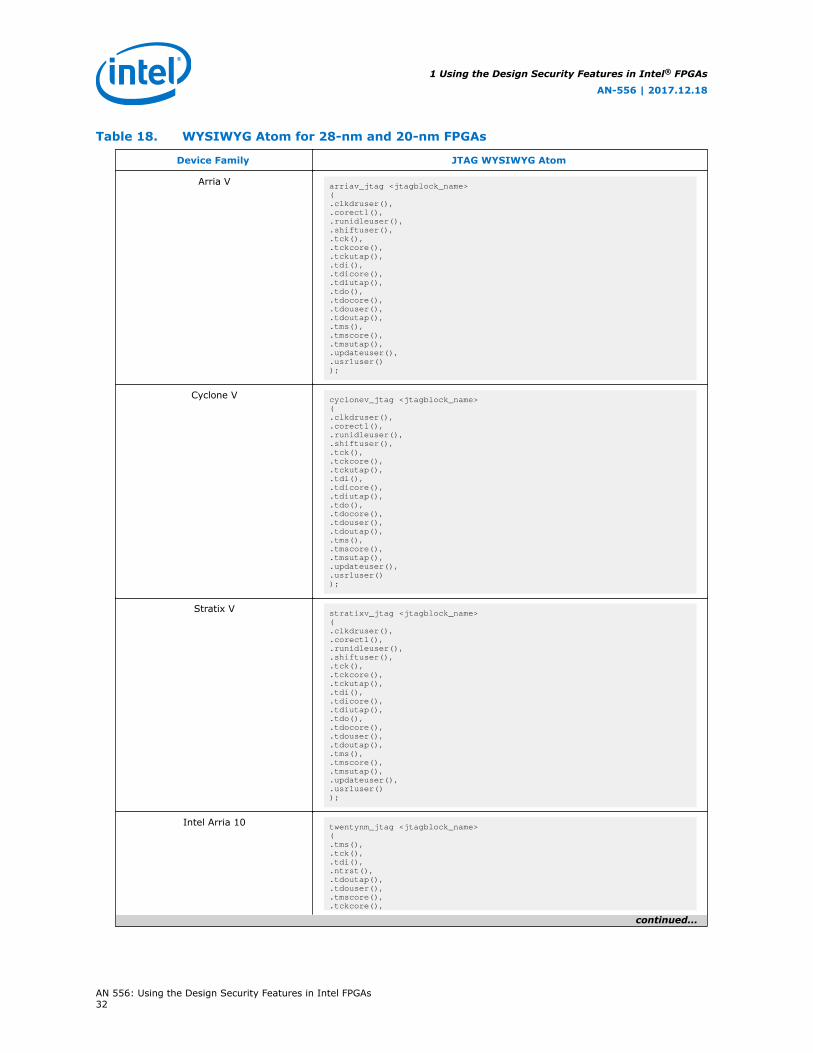
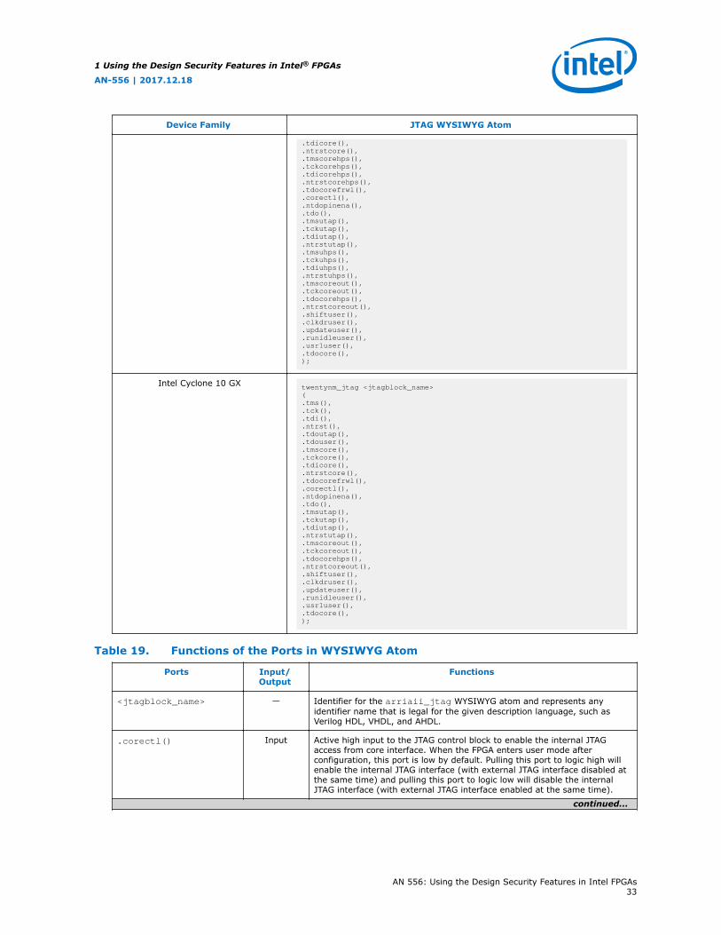
Table 18. WYSIWYG Atom for 28-nm and 20-nm FPGAs
Device Family JTAG WYSIWYG Atom
Arria V arriav_jtag <jtagblock_name>(.clkdruser(),.corectl(),.runidleuser(),.shiftuser(),.tck(),.tckcore(),.tckutap(),.tdi(),.tdicore(),.tdiutap(),.tdo(),.tdocore(),.tdouser(),.tdoutap(),.tms(),.tmscore(),.tmsutap(),.updateuser(),.usr1user());
Cyclone V cyclonev_jtag <jtagblock_name>(.clkdruser(),.corectl(),.runidleuser(),.shiftuser(),.tck(),.tckcore(),.tckutap(),.tdi(),.tdicore(),.tdiutap(),.tdo(),.tdocore(),.tdouser(),.tdoutap(),.tms(),.tmscore(),.tmsutap(),.updateuser(),.usr1user());
Stratix V stratixv_jtag <jtagblock_name>(.clkdruser(),.corectl(),.runidleuser(),.shiftuser(),.tck(),.tckcore(),.tckutap(),.tdi(),.tdicore(),.tdiutap(),.tdo(),.tdocore(),.tdouser(),.tdoutap(),.tms(),.tmscore(),.tmsutap(),.updateuser(),.usr1user());
Intel Arria 10 twentynm_jtag <jtagblock_name>(.tms(),.tck(),.tdi(),.ntrst(),.tdoutap(),.tdouser(),.tmscore(),.tckcore(),
continued...
1 Using the Design Security Features in Intel® FPGAs
AN-556 | 2017.12.18
AN 556: Using the Design Security Features in Intel FPGAs32
Device Family JTAG WYSIWYG Atom
.tdicore(),
.ntrstcore(),
.tmscorehps(),
.tckcorehps(),
.tdicorehps(),
.ntrstcorehps(),
.tdocorefrwl(),
.corectl(),
.ntdopinena(),
.tdo(),
.tmsutap(),
.tckutap(),
.tdiutap(),
.ntrstutap(),
.tmsuhps(),
.tckuhps(),
.tdiuhps(),
.ntrstuhps(),
.tmscoreout(),
.tckcoreout(),
.tdocorehps(),
.ntrstcoreout(),
.shiftuser(),
.clkdruser(),
.updateuser(),
.runidleuser(),
.usr1user(),
.tdocore(),);
Intel Cyclone 10 GX twentynm_jtag <jtagblock_name>(.tms(),.tck(),.tdi(),.ntrst(),.tdoutap(),.tdouser(),.tmscore(),.tckcore(),.tdicore(),.ntrstcore(),.tdocorefrwl(),.corectl(),.ntdopinena(),.tdo(),.tmsutap(),.tckutap(),.tdiutap(),.ntrstutap(),.tmscoreout(),.tckcoreout(),.tdocorehps(),.ntrstcoreout(),.shiftuser(),.clkdruser(),.updateuser(),.runidleuser(),.usr1user(),.tdocore(),);
Table 19. Functions of the Ports in WYSIWYG Atom
Ports Input/Output
Functions
<jtagblock_name> — Identifier for the arriaii_jtag WYSIWYG atom and represents anyidentifier name that is legal for the given description language, such asVerilog HDL, VHDL, and AHDL.
.corectl() Input Active high input to the JTAG control block to enable the internal JTAGaccess from core interface. When the FPGA enters user mode afterconfiguration, this port is low by default. Pulling this port to logic high willenable the internal JTAG interface (with external JTAG interface disabled atthe same time) and pulling this port to logic low will disable the internalJTAG interface (with external JTAG interface enabled at the same time).
continued...
1 Using the Design Security Features in Intel® FPGAs
AN-556 | 2017.12.18
AN 556: Using the Design Security Features in Intel FPGAs33

Ports Input/Output
Functions
.tckcore() Input Core TCK signal. (20)
.tdicore() Input Core TDI signal. (20)
.tdocore() Output Core TDO signal. (20)
.tmscore() Input Core TMS signal. (20)
.clkdruser() Input/Output These ports are not used for enabling the JTAG secure mode using theinternal JTAG interface, hence you can leave them unconnected.
.runidleuser()
.shiftuser()
.tck()
.tckutap()
.tdi()
.tdiutap()
.tdo()
.tdouser()
.tdoutap()
.tms()
.tmsutap()
.updateuser()
.usr1user()
Related Links
• EthernetBlaster Communications Cable User Guide
• EthernetBlaster II Communications Cable User GuideProvides more information about changing the TCK clock speed for Intel FPGAEthernet Cable.
• Device Datasheet for Arria II DevicesProvides more information about the specific voltages required using the JTAGdownload cable.
• DC and Switching Characteristics for Stratix IV DevicesProvides more information about the specific voltages required using the JTAGdownload cable.
• Arria V Device DatasheetProvides more information about the specific voltages required using the JTAGdownload cable.
• Cyclone V Device DatasheetProvides more information about the specific voltages required using the JTAGdownload cable.
(20) For external JTAG interface, refer to the respective device datasheet for the JTAG configurationtiming specification. For internal JTAG interface, you must perform timing constraint andtiming closure analysis on these paths to meet the setup or hold time requirement.
1 Using the Design Security Features in Intel® FPGAs
AN-556 | 2017.12.18
AN 556: Using the Design Security Features in Intel FPGAs34

• Stratix V Device DatasheetProvides more information about the specific voltages required using the JTAGdownload cable.
• Intel Arria 10 Device DatasheetProvides more information about the specific voltages required using the JTAGdownload cable.
• Intel Cyclone 10 GX Device DatasheetProvides more information about the specific voltages required using the JTAGdownload cable.
• Stratix V E, GS, and GX Device Family Pin Connection Guidelines
• Stratix V GT Device Family Pin Connection Guidelines
• Arria V GT, GX, ST and SX Device Family Pin Connection Guidelines
• Arria V GZ Device Family Pin Connection Guidelines
• Stratix IV GX and E Device Family Pin Connection Guidelines
• Stratix IV GT Device Family Pin Connection Guidelines
• Arria II Device Family Pin Connection Guidelines
• Intel Arria 10 GX, GT, and SX Device Family Pin Connection Guidelines
1.8.2 Design Example for JTAG Secure Mode
This design example demonstrates
• The instantiation of an internal JTAG WYSIWYG atom.
• The execution of the LOCK and UNLOCK JTAG instructions through user logicimplementation in the Intel Quartus Prime software.
This reference design is targeted on the Arria V device with the tamper-protection bitenabled. This design example is applicable to other 28-nm FPGAs.
Related Links
AN 556 Design Files
1.8.2.1 Design Example Intel Quartus Prime Design Components
Table 20. Intel Quartus Prime Design Components for the Arria V Device
Component Function and Description
JTAG_Lock_Unlock.bdf The top entity of the reference design.
JTAG_Lock_Unlock_wysiwyg.v The Verilog code for the Arria V device WYSIWYG atominstatiation. You need to modify this code according to Table18 on page 32 for compliance with other 28-nm FPGAs.
continued...
1 Using the Design Security Features in Intel® FPGAs
AN-556 | 2017.12.18
AN 556: Using the Design Security Features in Intel FPGAs35

Component Function and Description
ALTINT_OSC.v A IP core instantiation of an internal oscillator clock source.In this reference design, the clock source from the internaloscillator is used to drive the user logic to eliminate theneed of an external clock source.
User_logic_control_block.v An example Verilog file that executes JTAG instructionsusing Arria V device WYSIWYG atom. You can modify thiscode to fit your design requirements and restrictions, orreplace this code with another similar implementation.
Pulse_nconfig.jam Use this JAM file to execute the PULSE_NCONFIG JTAGinstruction to verify the JTAG secure mode as shown in Verifying JTAG Secure Mode on page 37. This file isoptional and can be replaced with other methods to verifythe JTAG secure mode.
1.8.2.2 LOCK and UNLOCK JTAG Instructions
When you configure this reference design into an Arria V device with thetamper-protection bit enabled, the Arria V device is in JTAG secure mode after powerup and configuration, whereby you can only execute mandatory JTAG instructions.
To disable the JTAG secure mode, you can trigger the start_unlock port of the userlogic to issue the UNLOCK JTAG instruction. After the start_unlock port goes high,the UNLOCK JTAG instruction is issued. After the UNLOCK JTAG instruction is issued,the device exits from JTAG secure mode, whereby both mandatory and non-mandatory JTAG instructions are allowed.
Figure 4. LOCK or UNLOCK JTAG Instruction Execution
Start
Enable the Internal JTAGInterface, corectl = 1
Shift the JTAG Instruction to the TDI Core.
start_unlock orstart_lock
= 1?
no
yes
End of InstructionLength?
no
yes
Move the TAP ControllerState Machine from the RESET State to the SHIFT_IR State by Controlling the TMS Core.
Move the TAP ControllerState Machine from theSHIFT_IR State to theIDLE State.
End
The start_lock port in the user logic triggers the execution of the LOCK JTAGinstruction. The function of the LOCK JTAG instruction is to put the device back intoJTAG secure mode.
1 Using the Design Security Features in Intel® FPGAs
AN-556 | 2017.12.18
AN 556: Using the Design Security Features in Intel FPGAs36
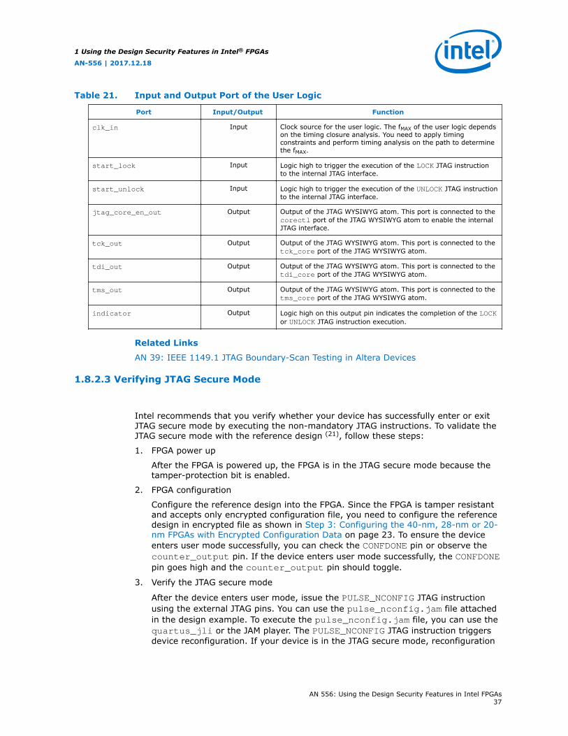
Table 21. Input and Output Port of the User Logic
Port Input/Output Function
clk_in Input Clock source for the user logic. The fMAX of the user logic dependson the timing closure analysis. You need to apply timingconstraints and perform timing analysis on the path to determinethe fMAX.
start_lock Input Logic high to trigger the execution of the LOCK JTAG instructionto the internal JTAG interface.
start_unlock Input Logic high to trigger the execution of the UNLOCK JTAG instructionto the internal JTAG interface.
jtag_core_en_out Output Output of the JTAG WYSIWYG atom. This port is connected to thecorectl port of the JTAG WYSIWYG atom to enable the internalJTAG interface.
tck_out Output Output of the JTAG WYSIWYG atom. This port is connected to thetck_core port of the JTAG WYSIWYG atom.
tdi_out Output Output of the JTAG WYSIWYG atom. This port is connected to thetdi_core port of the JTAG WYSIWYG atom.
tms_out Output Output of the JTAG WYSIWYG atom. This port is connected to thetms_core port of the JTAG WYSIWYG atom.
indicator Output Logic high on this output pin indicates the completion of the LOCKor UNLOCK JTAG instruction execution.
Related Links
AN 39: IEEE 1149.1 JTAG Boundary-Scan Testing in Altera Devices
1.8.2.3 Verifying JTAG Secure Mode
Intel recommends that you verify whether your device has successfully enter or exitJTAG secure mode by executing the non-mandatory JTAG instructions. To validate theJTAG secure mode with the reference design (21), follow these steps:
1. FPGA power up
After the FPGA is powered up, the FPGA is in the JTAG secure mode because thetamper-protection bit is enabled.
2. FPGA configuration
Configure the reference design into the FPGA. Since the FPGA is tamper resistantand accepts only encrypted configuration file, you need to configure the referencedesign in encrypted file as shown in Step 3: Configuring the 40-nm, 28-nm or 20-nm FPGAs with Encrypted Configuration Data on page 23. To ensure the deviceenters user mode successfully, you can check the CONFDONE pin or observe thecounter_output pin. If the device enters user mode successfully, the CONFDONEpin goes high and the counter_output pin should toggle.
3. Verify the JTAG secure mode
After the device enters user mode, issue the PULSE_NCONFIG JTAG instructionusing the external JTAG pins. You can use the pulse_nconfig.jam file attachedin the design example. To execute the pulse_nconfig.jam file, you can use thequartus_jli or the JAM player. The PULSE_NCONFIG JTAG instruction triggersdevice reconfiguration. If your device is in the JTAG secure mode, reconfiguration
1 Using the Design Security Features in Intel® FPGAs
AN-556 | 2017.12.18
AN 556: Using the Design Security Features in Intel FPGAs37

is not taking place because the PULSE_NCONFIG JTAG instruction is anon-mandatory JTAG instruction. You can confirm this by observing the CONFDONEpin and the counter_output pin. If reconfiguration did not take place, theCONFDONE pin stays high and the counter_output pin continues to toggle.
4. Execute the UNLOCK JTAG instruction
Pull the start_unlock port of the user logic to logic high. After the UNLOCK JTAGinstruction is complete, the indicator port goes high.
5. Verify the JTAG secure mode
After the UNLOCK JTAG instruction is completed, issue the PULSE_NCONFIG JTAGinstruction again using the external JTAG pins. If your device is not in the JTAGsecure mode, the PULSE_NCONFIG JTAG instruction triggers devicereconfiguration. You can observe the CONFDONE pin and the counter_output pinto monitor the device reconfiguration. The CONFDONE pin goes from high to lowand the counter_output pin stops toggling during device reconfiguration.
Related Links
AN 425: Using the Command-Line Jam STAPL Solution for Device ProgrammingProvides more information about quartus_jli .
1.9 Document Revision History for AN 556: Using the DesignSecurity Features in Intel FPGAs
Date Version Changes
December 2017 2017.12.18 • Added support for Intel Cyclone 10 GX device family.• Updated the "Specifications for Key Programming" table: Updated the
Non-Volatile Key and Volatile Key descriptions for TCK period.• Updated the "Security Mode Verification for 20-nm FPGAs" table:
Added footnotes for bits 11 and 13 to clarify that these bits are notapplicable Intel Cyclone 10 GX devices.
• Updated for latest Intel branding standards.• Updated --lockto=<FILE_NAME.qlk> security option description
in Security Options in Qcrypt Tool table.• Made minor text edits to the document.
June 2016 2016.06.01 • Added Arria 10 Qcrypt Tool information.• Added information about tamper-protection bit and JTAG Secure can
be enabled separately in 20-nm FPGAs.• Added software requirements for 20-nm FPGAs.• Added two additional steps for 20-nm FPGAs in Generating Single-
Device .ekp File and Encrypting Configuration File using Intel QuartusPrime Software.
• Added 20-nm FPGA JTAG Secure verification methods.• Added note about EXTEST_PULSE, EXTEST_TRAIN, KEY_VERIFY JTAG
instructions can be used during JTAG Secure mode.• Updated Arria 10 JTAG atom.• Added separate security approach for 20-nm FPGAs.
continued...
(21) You should only apply these steps on an FPGA with the tamper-protection bit enabled.
1 Using the Design Security Features in Intel® FPGAs
AN-556 | 2017.12.18
AN 556: Using the Design Security Features in Intel FPGAs38

Date Version Changes
• Added note about encryption and compression cannot be usedsimultaneously in 20-nm FPGAs.
• Updated TCK period non-volatile key specification for 20-nm FPGAs.• Added note about USB-Blaster supports volatile and non-volatile key
for 20-nm FPGAs.
November 2015 2015.11.02 • Added note about user need set the TCK speed to required TCKperiod for EthernetBlaster II and added link EthernetBlaster IICommunications Cable User Guide.
• Changed instances of Quartus II to Quartus Prime.
June 2015 2015.06.15 Added link to JTAG Secure Mode Design Example.
May 2015 2015.05.04 Corrected the total number of character in .key file example.
January 2015 2015.01.23 • Added 20-nm FPGAs (Arria 10) support.• Added JAM file example for 20-nm.• Added Security Mode Verification for 20-nm table.• Added JTAG WYSIWYG atom for Arria 10.• Added AES modes in Altera FPGAs.
December 2014 2014.12.15 Added USB-Blaster II support for non-volatile security key programming.
September 2014 2014.09.30 • Added example .key file in How to Generate the Single-Device .ekpFile and Encrypt the Configuration File using Quartus II Software.
• Removed VCCBAT voltage guideline and added device family pinconnection guidelines links for updated values in HardwareRequirements.
• Added note to modes with tamper protection in Security ModeVerification for 28-nm FPGAs.
• Added Verification During JTAG Secure Mode subsection to tamper bitprotection settings during JTAG Secure mode.
May 2014 2014.05.19 Updated the Non-Volatile and Volatile Key Storage section to includeinformation on using valid MSEL pin settings.
June 2013 2013.06.19 • Updated the Design Security Approach for FPGAs table to includemore design security features.
• Updated the Non-Volatile and Volatile Key Storage section to includedetails on both volatile and non-volatile key storage.
• Updated the Key Programming section to include support for both28-nm and 40-nm FPGAs using the System General programmingtool.
• Updated the Hardware Requirements section to update theSpecifications for Key Programming table.
• Updated the Steps for Implementing a Secure Configuration Flowsection.
• Updated the Step 1: Generate the .ekp File and EncryptConfiguration File, Step 2a: Program the Volatile Key into the FPGAs,and Step 2b: Program the Volatile Key into the FPGAs sections.
• Updated the How to Generate the Single-Device .ekp File and Encryptthe Configuration File using Quartus II Software to includeinformation about the encryption key for 28-nm and 40-nm FPGAs.
• Updated the Security Mode Verification section to update the securitymode and its associated bit values for both 28-nm and 40-nm FPGAs.
• Updated the JTAG Secure Mode for 28-nm FPGAs section to includemore information about the mandatory and non-mandatory JTAGinstructions, internal JTAG interface and external JTAG interface,WYSIWYG atom functions, and design example for JTAG securemode.
• Moved all links in all topics to the Related Information section foreasy reference.
continued...
1 Using the Design Security Features in Intel® FPGAs
AN-556 | 2017.12.18
AN 556: Using the Design Security Features in Intel FPGAs39

Date Version Changes
June 2012 2.1 • Updated Table 1 and Table 3.• Updated .ekp file verification error information.• Updated "Hardware Requirements" section.
June 2011 2.0 • Updated application note for the Quartus II software version 11.0release.
• Changed the specific device names to 40- or 28-nm FPGAs.• Added "Security Mode Verifcation" and "JTAG Secure Mode for 28-nm
FPGAs" sections.• Added Table 1.• Added Table 5.• Added Example 3, Example 4, and Example 5.• Updated Figure 1.• Minor text edits.
June 2009 1.1 • Updated "Introduction" on page 1.• Updated "Overview of the Design Security Feature" on page 2.• Updated "Security Encryption Algorithm" on page 2.• Updated "Non-Volatile and Volatile Key Storage" on page 3.• Updated (Note 3) of Table 2 on page 4.• Updated "Hardware and Software Requirements" on page 4.• Updated (Note 1) of Table 3 on page 5.• Updated "Steps for Implementing a Secure Configuration Flow" on
page 5.• Updated "Step 2a: Program the Volatile Key into the Arria II GX or
Stratix IV Devices" on page 17.• Updated "Step 2b: Program the Non-Volatile Key into the Arria II GX
or Stratix IV Devices" on page 18.• Updated "Step 3: Configure the Arria II GX or Stratix IV Devices with
Encrypted Configuration Data" on page 24.• Added Table 3 on page 28.• Updated Figure 1 on page 6 and Figue 26 on page 29.
March 2009 1.0 Initial release.
1 Using the Design Security Features in Intel® FPGAs
AN-556 | 2017.12.18
AN 556: Using the Design Security Features in Intel FPGAs40