PCM1803A Single-Ended, Analog-Input 24-Bit, 96 … · BCK V IN L Reference V REF 1 V REF 2 V IN R...
27
BCK V IN L Reference V REF 1 V REF 2 V IN R Delta-Sigma Modulator Delta-Sigma Modulator ×1/64 , ×1/128 Decimation Filter With High-Pass Filter Power Supply AGND V CC V DD DGND Clock and Timing Control Serial Interface Mode/ Format Control LRCK DOUT FMT0 FMT1 MODE0 MODE1 BYPAS OSR PDWN SCKI B0004-06 TEST Copyright © 2016, Texas Instruments Incorporated Product Folder Sample & Buy Technical Documents Tools & Software Support & Community An IMPORTANT NOTICE at the end of this data sheet addresses availability, warranty, changes, use in safety-critical applications, intellectual property matters and other important disclaimers. PRODUCTION DATA. PCM1803A SLES142B – JUNE 2005 – REVISED JULY 2016 PCM1803A Single-Ended, Analog-Input 24-Bit, 96-kHz Stereo A/D Converter 1 1 Features 1• 24-Bit Delta-Sigma Stereo A/D Converter • Single-Ended Voltage Input: 3 V p-p • Oversampling Decimation Filter: – Oversampling Frequency: ×64, ×128 – Pass-Band Ripple: ±0.05 dB – Stop-Band Attenuation: –65 dB – On-Chip High-Pass Filter: 0.84 Hz (44.1 kHz) • High-Performance: – THD+N: –95 dB (Typically) – SNR: 103 dB (Typically) – Dynamic Range: 103 dB (Typically) • PCM Audio Interface: – Master or Slave Mode Selectable – Data Formats: – 24-Bit Left-Justified – 24-Bit I 2 S – 20-, 24-Bit Right-Justified • Sampling Rate: 16 kHz to 96 kHz • System Clock: 256 f S , 384 f S , 512 f S , 768 f S • Dual Power Supplies: 5 V for Analog, 3.3 V for Digital • Package: 20-Pin SSOP 2 Applications • AV Amplifier Receivers • MD Players • CD Recorders • Multitrack Receivers • Electric Musical Instruments 3 Description The PCM1803A device is high-performance, low- cost, single-chip stereo analog-to-digital converter with single-ended analog voltage input. The PCM1803A uses a delta-sigma modulator with 64- and 128-times oversampling, and includes a digital decimation filter and high-pass filter, which removes the DC component of the input signal. For various applications, the PCM1803A supports master and slave modes and four data formats in serial interface. The PCM1803A is suitable for a wide variety of cost- sensitive consumer applications where good performance and operation from a 5-V analog supply and 3.3-V digital supply are required. The PCM1803A is fabricated using a highly-advanced CMOS process and is available in a small 20-pin SSOP package. Device Information (1) PART NUMBER PACKAGE BODY SIZE (NOM) PCM1803A SSOP (20) 7.20 mm × 5.30 mm (1) For all available packages, see the orderable addendum at the end of the data sheet. Functional Block Diagram
Transcript of PCM1803A Single-Ended, Analog-Input 24-Bit, 96 … · BCK V IN L Reference V REF 1 V REF 2 V IN R...

BCKVINL
Reference
VREF1
VREF2
VINR
Delta-Sigma
Modulator
Delta-Sigma
Modulator
×1/64 , ×1/128
Decimation
Filter
With
High-Pass Filter
Power Supply
AGNDVCC VDDDGND
Clock and Timing Control
Serial
Interface
Mode/
Format
Control
LRCK
DOUT
FMT0
FMT1
MODE0
MODE1
BYPAS
OSR
PDWN
SCKI
B0004-06
TEST
Copyright © 2016, Texas Instruments Incorporated
Product
Folder
Sample &Buy
Technical
Documents
Tools &
Software
Support &Community
An IMPORTANT NOTICE at the end of this data sheet addresses availability, warranty, changes, use in safety-critical applications,intellectual property matters and other important disclaimers. PRODUCTION DATA.
PCM1803ASLES142B –JUNE 2005–REVISED JULY 2016
PCM1803A Single-Ended, Analog-Input 24-Bit, 96-kHz Stereo A/D Converter
1
1 Features1• 24-Bit Delta-Sigma Stereo A/D Converter• Single-Ended Voltage Input: 3 Vp-p
• Oversampling Decimation Filter:– Oversampling Frequency: ×64, ×128– Pass-Band Ripple: ±0.05 dB– Stop-Band Attenuation: –65 dB– On-Chip High-Pass Filter: 0.84 Hz (44.1 kHz)
• High-Performance:– THD+N: –95 dB (Typically)– SNR: 103 dB (Typically)– Dynamic Range: 103 dB (Typically)
• PCM Audio Interface:– Master or Slave Mode Selectable– Data Formats:
– 24-Bit Left-Justified– 24-Bit I2S– 20-, 24-Bit Right-Justified
• Sampling Rate: 16 kHz to 96 kHz• System Clock: 256 fS, 384 fS, 512 fS, 768 fS• Dual Power Supplies: 5 V for Analog, 3.3 V for
Digital• Package: 20-Pin SSOP
2 Applications• AV Amplifier Receivers• MD Players• CD Recorders• Multitrack Receivers• Electric Musical Instruments
3 DescriptionThe PCM1803A device is high-performance, low-cost, single-chip stereo analog-to-digital converterwith single-ended analog voltage input. ThePCM1803A uses a delta-sigma modulator with 64-and 128-times oversampling, and includes a digitaldecimation filter and high-pass filter, which removesthe DC component of the input signal. For variousapplications, the PCM1803A supports master andslave modes and four data formats in serial interface.The PCM1803A is suitable for a wide variety of cost-sensitive consumer applications where goodperformance and operation from a 5-V analog supplyand 3.3-V digital supply are required. The PCM1803Ais fabricated using a highly-advanced CMOS processand is available in a small 20-pin SSOP package.
Device Information(1)
PART NUMBER PACKAGE BODY SIZE (NOM)PCM1803A SSOP (20) 7.20 mm × 5.30 mm
(1) For all available packages, see the orderable addendum atthe end of the data sheet.
Functional Block Diagram

2
PCM1803ASLES142B –JUNE 2005–REVISED JULY 2016 www.ti.com
Product Folder Links: PCM1803A
Submit Documentation Feedback Copyright © 2005–2016, Texas Instruments Incorporated
Table of Contents1 Features .................................................................. 12 Applications ........................................................... 13 Description ............................................................. 14 Revision History..................................................... 25 Pin Configuration and Functions ......................... 36 Specifications......................................................... 4
6.1 Absolute Maximum Ratings ...................................... 46.2 ESD Ratings.............................................................. 46.3 Recommended Operating Conditions....................... 46.4 Thermal Information .................................................. 56.5 Electrical Characteristics........................................... 56.6 Typical Characteristics .............................................. 7
7 Detailed Description ............................................ 107.1 Overview ................................................................. 107.2 Functional Block Diagram ....................................... 107.3 Feature Description................................................. 10
7.4 Device Functional Modes........................................ 128 Application and Implementation ........................ 17
8.1 Application Information............................................ 178.2 Typical Application ................................................. 17
9 Power Supply Recommendations ...................... 1910 Layout................................................................... 19
10.1 Layout Guidelines ................................................. 1910.2 Layout Example .................................................... 20
11 Device and Documentation Support ................. 2111.1 Receiving Notification of Documentation Updates 2111.2 Community Resources.......................................... 2111.3 Trademarks ........................................................... 2111.4 Electrostatic Discharge Caution............................ 2111.5 Glossary ................................................................ 21
12 Mechanical, Packaging, and OrderableInformation ........................................................... 21
4 Revision HistoryNOTE: Page numbers for previous revisions may differ from page numbers in the current version.
Changes from Revision A (August 2006) to Revision B Page
• Added ESD Ratings table, Feature Description section, Device Functional Modes, Application and Implementationsection, Power Supply Recommendations section, Layout section, Device and Documentation Support section, andMechanical, Packaging, and Orderable Information section. ................................................................................................. 1
• Changed RθJA value from 115 °C/W to 84.4 °C/W in Thermal Information ............................................................................ 5• Changed the Thermal Information table ................................................................................................................................ 5

Not to scale
1VINL 20 MODE1
2VINR 19 MODE0
3VREF1 18 FMT1
4VREF2 17 FMT0
5VCC 16 OSR
6AGND 15 SCKI
7PDWN 14 VDD
8BYPAS 13 DGND
9TEST 12 DOUT
10LRCK 11 BCK
3
PCM1803Awww.ti.com SLES142B –JUNE 2005–REVISED JULY 2016
Product Folder Links: PCM1803A
Submit Documentation FeedbackCopyright © 2005–2016, Texas Instruments Incorporated
(1) Schmitt-trigger input(2) Schmitt-trigger input with internal pulldown (50 kΩ, typically), 5-V tolerant(3) Schmitt-trigger input, 5-V tolerant
5 Pin Configuration and Functions
DB Package20-Pin SSOP
Top View
Pin FunctionsPIN
I/O DESCRIPTIONNAME NO.AGND 6 – Analog GNDBCK 11 I/O Audio data bit clock input/output (1)
BYPAS 8 I HPF bypass control. LOW: Normal mode (DC reject); HIGH: Bypass mode (through) (2)
DGND 13 – Digital GNDDOUT 12 O Audio data digital outputFMT0 17 I Audio data format select input 0. See Data Format. (2)
FMT1 18 I Audio data format select input 1. See Data Format. (2)
LRCK 10 I/O Audio data latch enable input/output (1)
MODE0 19 I Mode select input 0. See Data Format. (2)
MODE1 20 I Mode select input 1. See Data Format. (2)
OSR 16 I Oversampling ratio select input. LOW: ×64 fS, HIGH: ×128 fS(2)
PDWN 7 I Power-down control, active-low (2)
SCKI 15 I System clock input: 256 fS, 384 fS, 512 fS, or 768 fS(3)
TEST 9 I Test, must be connected to DGND (2)
VCC 5 – Analog power supply, 5-VVDD 14 – Digital power supply, 3.3-VVINL 1 I Analog input, L-channelVINR 2 I Analog input, R-channelVREF1 3 – Reference-voltage-1 decoupling capacitorVREF2 4 – Reference-voltage-2 decoupling capacitor

4
PCM1803ASLES142B –JUNE 2005–REVISED JULY 2016 www.ti.com
Product Folder Links: PCM1803A
Submit Documentation Feedback Copyright © 2005–2016, Texas Instruments Incorporated
(1) Stresses beyond those listed under Absolute Maximum Ratings may cause permanent damage to the device. These are stress ratingsonly, which do not imply functional operation of the device at these or any other conditions beyond those indicated under RecommendedOperating Conditions. Exposure to absolute-maximum-rated conditions for extended periods may affect device reliability.
6 Specifications
6.1 Absolute Maximum Ratingsover operating free-air temperature range (unless otherwise noted) (1)
MIN MAX UNIT
Supply voltageVCC –0.3 6.5
VVDD –0.3 4
Ground voltage differences AGND, DGND ±0.1 V
Digital input voltage, VI
LRCK, BCK, DOUT –0.3 (VDD + 0.3) < 4VPDWN, BYPAS, TEST, SCKI, OSR, FMT0, FMT1,
MODE0, MODE1 –0.3 6.5
Analog input voltage, VI VINL, VINR, VREF1, VREF2 –0.3 (VCC + 0.3) < 6.5 VInput current, II Any pins except supplies ±10 mAAmbient temperature under bias, Tbias –40 125 °CJunction temperature, TJ 150 °CLead temperature (soldering) 5 s 260 °CPackage temperature (IR reflow, peak) 260 °CStorage temperature, Tstg –55 150 °C
(1) JEDEC document JEP155 states that 500-V HBM allows safe manufacturing with a standard ESD control process.(2) JEDEC document JEP157 states that 250-V CDM allows safe manufacturing with a standard ESD control process.
6.2 ESD RatingsVALUE UNIT
V(ESD)Electrostaticdischarge
Human-body model (HBM), per ANSI/ESDA/JEDEC JS-001 (1) ±4000V
Charged-device model (CDM), per JEDEC specification JESD22-C101 (2) ±1500
6.3 Recommended Operating Conditionsover operating free-air temperature range
MIN NOM MAX UNITAnalog supply voltage, VCC 4.5 5 5.5 VDigital supply voltage, VDD 2.7 3.3 3.6 VAnalog input voltage, full-scale (–0 dB) 3 Vp-pDigital input logic family TTL
Digital input clock frequencySystem clock 8.192 49.152 MHzSampling clock 32 96 kHz
Digital output load capacitance 20 pFOperating free-air temperature, TA –25 85 °C

5
PCM1803Awww.ti.com SLES142B –JUNE 2005–REVISED JULY 2016
Product Folder Links: PCM1803A
Submit Documentation FeedbackCopyright © 2005–2016, Texas Instruments Incorporated
(1) For more information about traditional and new thermal metrics, see the Semiconductor and IC Package Thermal Metrics applicationreport.
6.4 Thermal Information
THERMAL METRIC (1)PCM1803A
UNITDB (SSOP)20 PINS
RθJA Junction-to-ambient thermal resistance 84.4 °C/WRθJC(top) Junction-to-case (top) thermal resistance 42.4 °C/WRθJB Junction-to-board thermal resistance 41.4 °C/WψJT Junction-to-top characterization parameter 8.3 °C/WψJB Junction-to-board characterization parameter 40.7 °C/WRθJC(bot) Junction-to-case (bottom) thermal resistance — °C/W
(1) Pins 10 to 11: LRCK, BCK (Schmitt-trigger input, in slave mode)(2) Pin 15: SCKI (Schmitt-trigger input, 5-V tolerant)(3) Pins 7 to 9, 16 to 20: PDWN, BYPAS, TEST, OSR, FMT0, FMT1, MODE0, MODE1 (Schmitt-trigger input, with 50-kΩ typical pulldown
resistor, 5-V tolerant)(4) Pins 10 to 12: LRCK, BCK (in master mode), DOUT
6.5 Electrical CharacteristicsAll specifications at TA = 25°C, VCC = 5 V, VDD = 3.3 V, master mode, fS = 44.1 kHz, system clock = 384 fS,oversampling ratio = ×128, 24-bit data (unless otherwise noted)
PARAMETER TEST CONDITIONS MIN TYP MAX UNITResolution 24 Bits
DATA FORMATAudio data interface format Left-justified, I2S, right-justifiedAudio data bit length 20, 24 BitsAudio data format MSB-first, 2s complement
fS Sampling frequency 16 44.1 96 kHz
System clock frequency
256 fS 4.096 11.2896 24.576
MHz384 fS 6.144 16.9344 36.864512 fS 8.192 22.5792 49.152768 fS 12.288 33.8688
INPUT LOGICVIH
(1)
Input logic-level voltage
2 VDD
VdcVIL
(1) 0 0.8VIH
(2) (3) 2 5.5VIL
(2) (3) 0 0.8IIH (1) (2)
Input logic-level current
VIN = VDD ±10
μAIIL (1) (2) VIN = 0 ±10IIH (3) VIN = VDD 65 100IIL (3) VIN = 0 ±10OUTPUT LOGICVOH
(4)Output logic-level voltage
IOUT = –4 mA 2.8Vdc
VOL(4) IOUT = 4 mA 0.5
DC ACCURACYGain mismatch, channel-to-channel ±1 ±3 % of FSRGain error ±2 ±4 % of FSRBipolar zero error HPF bypass ±0.4 % of FSR

6
PCM1803ASLES142B –JUNE 2005–REVISED JULY 2016 www.ti.com
Product Folder Links: PCM1803A
Submit Documentation Feedback Copyright © 2005–2016, Texas Instruments Incorporated
Electrical Characteristics (continued)All specifications at TA = 25°C, VCC = 5 V, VDD = 3.3 V, master mode, fS = 44.1 kHz, system clock = 384 fS,oversampling ratio = ×128, 24-bit data (unless otherwise noted)
PARAMETER TEST CONDITIONS MIN TYP MAX UNIT
(5) Analog performance specifications are tested using the System Two™ audio measurement system by Audio Precision™, using 400-HzHPF, 20-kHz LPF in rms mode.
(6) fS = 96 kHz, system clock = 256 fS, oversampling ratio = ×64.(7) Minimum load on DOUT (pin 12), BCK (pin 11), LRCK (pin 10)(8) Halt SCKI, BCK, LRCK
DYNAMIC PERFORMANCE (5)
THD+N Total harmonic distortion + noise
VIN = –0.5 dB, fS = 44.1 kHz –95 –89
dBVIN = –0.5 dB, fS = 96 kHz (6) –93VIN = –60 dB, fS = 44.1 kHz –41VIN = –60 dB, fS = 96 kHz (6) –41
Dynamic rangefS = 44.1 kHz, A-weighted 100 103
dBfS = 96 kHz, A-weighted (6) 103
SNR Signal-to-noise ratiofS = 44.1 kHz, A-weighted 100 103
dBfS = 96 kHz, A-weighted (6) 103
Channel separationfS = 44.1 kHz 95 98
dBfS = 96 kHz (6) 99
ANALOG INPUTVI Input voltage 0.6 × VCC Vp-p
Center voltage (VREF1) 0.5 × VCC VInput impedance 40 kΩ
DIGITAL FILTER PERFORMANCEPass band 0.454 × fS HzStop band 0.583 × fS HzPass-band ripple ±0.05 dBStop-band attenuation –65 dB
tGD Group delay time 17.4 / fS sHPF frequency response –3 dB 0.019 × fS mHz
POWER SUPPLY REQUIREMENTSVCC Supply voltage range
4.5 5 5.5 VdcVDD 2.7 3.3 3.6 Vdc
ICC
Supply current (7)
7.7 10 mAPower down (8) 5 μA
IDD
fS = 44.1 kHz 6.5 9 mAfS = 96 kHz (6) 11.7 mAPower down (8) 1 μA
Power dissipationfS = 44.1 kHz 60 80 mWfS = 96 kHz (6) 77 mWPower down (8) 28 μW
TEMPERATURE RANGETA Operating free-air temperature –40 85 °C
G005Normalized Frequency [ × fS/1000]
−100
−90
−80
−70
−60
−50
−40
−30
−20
−10
0
0.0 0.1 0.2 0.3 0.4
Am
plitu
de −
dB
G006Normalized Frequency [ × fS/1000]
−1.0
−0.8
−0.6
−0.4
−0.2
0.0
0.2
0 1 2 3 4
Am
plitu
de −
dB
G004Normalized Frequency [ × fS]
−1.0
−0.8
−0.6
−0.4
−0.2
0.0
0.2
0.0 0.1 0.2 0.3 0.4 0.5 0.6
Am
plitu
de −
dB
OversamplingRatio = 128 and 64
G003Normalized Frequency [ × fS]
−100
−90
−80
−70
−60
−50
−40
−30
−20
−10
0
0.00 0.25 0.50 0.75 1.00
Am
plitu
de −
dB
OversamplingRatio = 128 and 64
Normalized Frequency [ × fS]
−200
−150
−100
−50
0
50
0 8 16 24 32 40 48 56 64
Oversampling Ratio = 128
Am
plitu
de −
dB
G001 G002Normalized Frequency [ × fS]
−200
−150
−100
−50
0
50
0 8 16 24 32
Am
plitu
de −
dB
Oversampling Ratio = 64
7
PCM1803Awww.ti.com SLES142B –JUNE 2005–REVISED JULY 2016
Product Folder Links: PCM1803A
Submit Documentation FeedbackCopyright © 2005–2016, Texas Instruments Incorporated
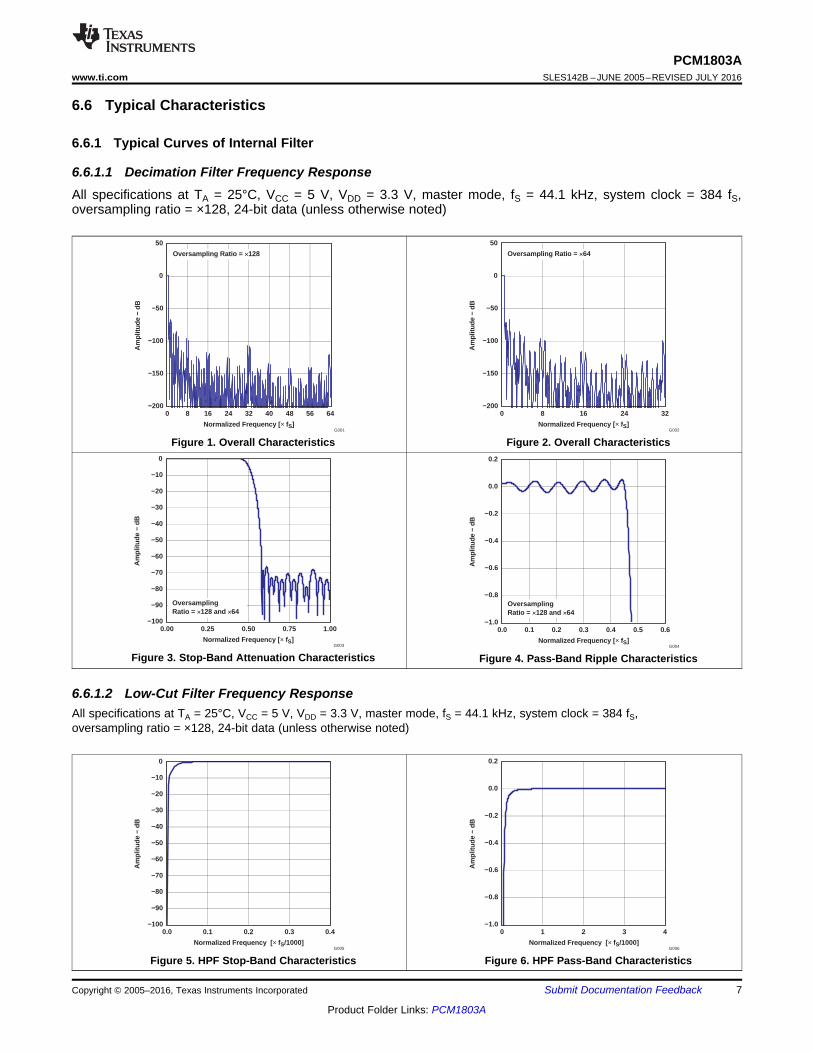
6.6 Typical Characteristics
6.6.1 Typical Curves of Internal Filter
6.6.1.1 Decimation Filter Frequency ResponseAll specifications at TA = 25°C, VCC = 5 V, VDD = 3.3 V, master mode, fS = 44.1 kHz, system clock = 384 fS,oversampling ratio = ×128, 24-bit data (unless otherwise noted)
Figure 1. Overall Characteristics Figure 2. Overall Characteristics
Figure 3. Stop-Band Attenuation Characteristics Figure 4. Pass-Band Ripple Characteristics
6.6.1.2 Low-Cut Filter Frequency ResponseAll specifications at TA = 25°C, VCC = 5 V, VDD = 3.3 V, master mode, fS = 44.1 kHz, system clock = 384 fS,oversampling ratio = ×128, 24-bit data (unless otherwise noted)
Figure 5. HPF Stop-Band Characteristics Figure 6. HPF Pass-Band Characteristics

−100
−99
−98
−97
−96
−95
−94
−93
−92
−91
−90
0 10 20 30 40
fSAMPLE Condition − kHz
TH
D+N
− T
otal
Har
mon
ic D
isto
rtion
+ N
oise
− d
B
44.1 96(2)48(1)
(1)fS = 48 kHz, System Clock = 256 f S, Oversampling Ratio = ×128.(2)fS = 96 kHz, System Clock = 256 f S, Oversampling Ratio = ×64.
G011
100
101
102
103
104
105
106
107
108
109
110
0 10 20 30 40
Dyn
amic
Ran
ge a
nd S
NR
− d
B
44.1 96(2)48(1)
SNR
Dynamic Range
fSAMPLE Condition − kHz
(1)fS = 48 kHz, System Clock = 256 f S, Oversampling Ratio = ×128.(2)fS = 96 kHz, System Clock = 256 f S, Oversampling Ratio = ×64.
G012
−100
−99
−98
−97
−96
−95
−94
−93
−92
−91
−90
4.25 4.50 4.75 5.00 5.25 5.50 5.75
VCC − Supply V oltage − V
TH
D+N
− T
otal
Har
mon
ic D
isto
rtion
+ N
oise
− d
B
G009 G010
100
101
102
103
104
105
106
107
108
109
110
4.25 4.50 4.75 5.00 5.25 5.50 5.75
VCC − Supply V oltage − V
Dyn
amic
Ran
ge a
nd S
NR
− d
B
SNR
Dynamic Range
G007
−100
−99
−98
−97
−96
−95
−94
−93
−92
−91
−90
−50 −25 0 25 50 75 100
TA − Free-Air T emperature − °C
TH
D+N
− T
otal
Har
mon
ic D
isto
rtion
+ N
oise
− d
B
100
101
102
103
104
105
106
107
108
109
110
−50 −25 0 25 50 75 100
G008TA − Free-Air T emperature − °C
Dyn
amic
Ran
ge a
nd S
NR
− d
B
SNR
Dynamic Range
8
PCM1803ASLES142B –JUNE 2005–REVISED JULY 2016 www.ti.com
Product Folder Links: PCM1803A
Submit Documentation Feedback Copyright © 2005–2016, Texas Instruments Incorporated
6.6.2 Typical Performance CurvesAll specifications at TA = 25°C, VCC = 5 V, VDD = 3.3 V, master mode, fS = 44.1 kHz, system clock = 384 fS,oversampling ratio = ×128, 24-bit data (unless otherwise noted)
Figure 7. Total Harmonic Distortion + Noise vsTemperature
Figure 8. Dynamic Range and Signal-to-Noise Ratio vsTemperature
Figure 9. Total Harmonic Distortion + Noise vs SupplyVoltage
Figure 10. Dynamic Range and Signal-to-Noise Ratio vsSupply Voltage
Figure 11. Total Harmonic Distortion + Noise vs fSAMPLECondition
Figure 12. Dynamic Range and Signal-to-Noise Ratio vsfSAMPLE Condition

0
5
10
15
0 10 20 30 40
I CC
and
ID
D −
Sup
ply
Cur
rent
− m
A
44.1 96(2)48(1)
ICC
fSAMPLE Condition − kHz
IDD
(1)fS = 48 kHz, System Clock = 256 f S, Oversampling Ratio = ×128.(2)fS = 96 kHz, System Clock = 256 f S, Oversampling Ratio = ×64.
G016
−100
−90
−80
−70
−60
−50
−40
−30
−20
−10
0
−100 −90 −80 −70 −60 −50 −40 −30 −20 −10 0
Signal Level − dB
TH
D+N
− T
otal
Har
mon
ic D
isto
rtion
+ N
oise
− d
B
G015
G014
f − Frequency − kHz
−140
−120
−100
−80
−60
−40
−20
0
0 5 10 15 20
Am
plitu
de −
dB
Input Level = −60 dBData Points = 8192
G013f − Frequency − kHz
−140
−120
−100
−80
−60
−40
−20
0
0 5 10 15 20
Input Level = −0.5 dBData Points = 8192
Am
plitu
de −
dB
9
PCM1803Awww.ti.com SLES142B –JUNE 2005–REVISED JULY 2016
Product Folder Links: PCM1803A
Submit Documentation FeedbackCopyright © 2005–2016, Texas Instruments Incorporated
6.6.3 Output Spectrum
Figure 13. Output Spectrum Figure 14. Output Spectrum
Figure 15. Total Harmonic Distortion + Noise vs Signal Level
6.6.4 Supply Current
Figure 16. Supply Current vs fSAMPLE Condition

BCKVINL
Reference
VREF1
VREF2
VINR
Delta-Sigma
Modulator
Delta-Sigma
Modulator
×1/64 , ×1/128
Decimation
Filter
With
High-Pass Filter
Power Supply
AGNDVCC VDDDGND
Clock and Timing Control
Serial
Interface
Mode/
Format
Control
LRCK
DOUT
FMT0
FMT1
MODE0
MODE1
BYPAS
OSR
PDWN
SCKI
B0004-06
TEST
Copyright © 2016, Texas Instruments Incorporated
10
PCM1803ASLES142B –JUNE 2005–REVISED JULY 2016 www.ti.com
Product Folder Links: PCM1803A
Submit Documentation Feedback Copyright © 2005–2016, Texas Instruments Incorporated
7 Detailed Description
7.1 OverviewThe PCM1803A is suitable for a wide variety of cost-sensitive consumer applications where good performanceand operation from a 5-V analog supply and 3.3-V digital supply are required. With hardware control andstraightforward operation, the PCM1803A can quickly be implemented into an application. The PCM1803Asupports sampling rates from 16 kHz to 96 kHz as well as left justified, right justified, and I2S formats, allowing itsuse in a variety of audio systems.
7.2 Functional Block Diagram
7.3 Feature Description
7.3.1 Hardware ControlPins FMT0, FMT1, OSR, BYPASS, MD0, and MD1 allow the device to be controlled by either tying these pins toGND, or VDD, as well as GPIO, from a host IC. These controls allow full configuration of the PCM1803A.
7.3.2 Power-On-Reset SequenceThe PCM1803A has an internal power-on-reset circuit, and initialization (reset) is performed automatically at thetime when power-supply voltage (VDD) exceeds 2.2 V (typical). While VDD < 2.2 V (typical) and for 1024 systemclock cycles after VDD > 2.2 V (typical), the PCM1803A stays in the reset state, and the digital output is forced tozero. The digital output becomes valid when a time period of 4480/fS has elapsed following release from thereset state. Figure 17 illustrates the internal power-on-reset timing and the digital output for power-on reset.

SCKI0.8 V
SCKI
2 V
tw(SCKL)tw(SCKH)
T0005B07
System Clock
2.6 V 2.2 V 1.8 V
Internal Reset
DOUT Zero Data Normal Data
Reset
VDD
Reset Removal
1024 System Clocks 4480 / fS
T0014-05
11
PCM1803Awww.ti.com SLES142B –JUNE 2005–REVISED JULY 2016
Product Folder Links: PCM1803A
Submit Documentation FeedbackCopyright © 2005–2016, Texas Instruments Incorporated
Feature Description (continued)
(1) Slave mode only
Figure 17. Internal Power-On-Reset Timing
7.3.3 System ClockThe PCM1803A supports 256 fS, 384 fS, 512 fS, and 768 fS as the system clock, where fS is the audio samplingfrequency. The system clock must be supplied on SCKI (pin 15).
The PCM1803A has a system clock-detection circuit that automatically senses if the system clock is operating at256 fS, 384 fS, 512 fS, or 768 fS in slave mode. In master mode, the system clock frequency must be selected byMODE0 (pin 19) and MODE1 (pin 20), and 768 fS is not available. The system clock is divided automatically into128 fS and 64 fS, and these frequencies are used to operate the digital filter and the delta-sigma modulator.
Table 1 shows the relationship of typical sampling frequency and system clock frequency, and Figure 18 showssystem clock timing.
Table 1. Sampling Frequency and System Clock Frequency
SAMPLING FREQUENCY (kHz)SYSTEM CLOCK FREQUENCY (MHz)
256 fS 384 fS 512 fS 768 fS(1)
32 8.1920 12.2880 16.3840 24.576044.1 11.2896 16.9344 22.5792 33.868848 12.2880 18.4320 24.5760 36.864064 16.3840 24.5760 32.7680 49.1520
88.2 22.5792 33.8688 45.1584 –96 24.5760 36.8640 49.1520 –
Figure 18. System Clock Timing

12
PCM1803ASLES142B –JUNE 2005–REVISED JULY 2016 www.ti.com
Product Folder Links: PCM1803A
Submit Documentation Feedback Copyright © 2005–2016, Texas Instruments Incorporated
Table 2. System Clock Timing RequirementsPARAMETER MIN MAX UNIT
tw(SCKH) System clock pulse duration, HIGH 8 nstw(SCKL) System clock pulse duration, LOW 8 ns
The quality of the system clock can influence the dynamic performance, because the PCM1803A operates basedon a system clock. Therefore, it may be required to consider the system-clock duty, jitter, and the time differencebetween system-clock transition and BCK or LRCK transition in the slave mode.
7.4 Device Functional Modes
7.4.1 Serial Audio Data InterfaceThe PCM1803A interfaces the audio system through BCK (pin 11), LRCK (pin 10), and DOUT (pin 12).
7.4.1.1 Interface ModeThe PCM1803A supports master mode and slave mode as interface modes, and they are selected by MODE1(pin 20) and MODE0 (pin 19) as shown in Table 3.
In master mode, the PCM1803A provides the timing of serial audio data communications between thePCM1803A and the digital audio processor or external circuit. While in slave mode, the PCM1803A receives thetiming for data transfers from an external controller.
Table 3. Interface ModeMODE1 MODE0 INTERFACE MODE
0 0 Slave mode (256 fS, 384 fS, 512 fS, 768 fS)0 1 Master mode (512 fS)1 0 Master mode (384 fS)1 1 Master mode (256 fS)
7.4.1.1.1 Master Mode
In master mode, BCK and LRCK work as output pins, and these pins are controlled by timing, which is generatedin the clock circuit of the PCM1803A. The frequency of BCK is fixed at LRCK × 64. The 768-fS system clock isnot available in master mode.
7.4.1.1.2 Slave Mode
In slave mode, BCK and LRCK work as input pins. The PCM1803A accepts the 64-BCK/LRCK or 48-BCK/LRCKformat (only for 384 fS and 768 fS system clocks), not the 32-BCK/LRCK format.
7.4.1.2 Data FormatThe PCM1803A supports four audio data formats in both master and slave modes, and the data formats areselected by FMT1 (pin 18) and FMT0 (pin 17) as shown in Table 4. Figure 19 illustrates the data formats in slaveand master modes.
Table 4. Data FormatsFORMAT FMT1 FMT0 DESCRIPTION
0 0 0 Left-justified, 24-bit1 0 1 I2S, 24-bit2 1 0 Right-justified, 24-bit3 1 1 Right-justified, 20-bit

LRCK Right-ChannelLeft-Channel
BCK
DOUT 24 22 23 24321
MSB LSB
22 23 24321
MSB LSB
LRCK Right-ChannelLeft-Channel
BCK
DOUT 20 18 19 20321
MSB LSB
18 19 20321
MSB LSB
LRCK Right-ChannelLeft-Channel
BCK
DOUT 22 23 24321
MSB LSB
22 23 24321
MSB LSB
BCK
LRCK Right-ChannelLeft-Channel
DOUT 122 23 24321
MSB LSB
22 23 24321
MSB LSB
24-Bit, MSB-First, Left-Justified
FORMAT 0: FMT[1:0] = 00
24-Bit, MSB-First, I 2S
FORMAT 1: FMT[1:0] = 01
24-Bit, MSB-First, Right-Justified
FORMAT 2: FMT[1:0] = 10
20-Bit, MSB-First, Right-Justified
FORMAT 3: FMT[1:0] = 1 1
T0016-11
13
PCM1803Awww.ti.com SLES142B –JUNE 2005–REVISED JULY 2016
Product Folder Links: PCM1803A
Submit Documentation FeedbackCopyright © 2005–2016, Texas Instruments Incorporated
Figure 19. Audio Data Formats (LRCK and BCK Work as Inputs in Slave Mode and as Outputs in MasterMode)
7.4.1.3 Interface TimingFigure 20 illustrates the interface timing in slave mode; Figure 21 and Figure 22 illustrate the interface timing inmaster mode.

BCK
LRCK
DOUT
t(BCKH)
t(BCKL)
t(CKLR)
t(LRCP)
t(BCKP) t(CKDO) t(LRDO)
0.5 VDD
0.5 VDD
0.5 VDD
T0018-02
BCK
LRCK
DOUT
t(BCKH)
t(BCKL)
t(LRHD)
t(LRCP)
t(LRSU)
t(BCKP) t(CKDO) t(LRDO)
1.4 V
1.4 V
0.5 VDD
T0017-02
14
PCM1803ASLES142B –JUNE 2005–REVISED JULY 2016 www.ti.com
Product Folder Links: PCM1803A
Submit Documentation Feedback Copyright © 2005–2016, Texas Instruments Incorporated
(1) Timing measurement reference level is 1.4 V for input and 0.5 VDD for output. Rising and falling time is measured from 10% to 90% ofIN/OUT signal swing. Load capacitance of DOUT is 20 pF. t(SCKI) means SCKI period time.
Figure 20. Audio Data Interface Timing (Slave Mode: LRCK and BCK Work as Inputs)
Table 5. Audio Data Interface Slave Mode Timing Requirements (1)
PARAMETER MIN TYP MAX UNITt(BCKP) BCK period 1/(64 fS) nst(BCKH) BCK pulse duration, HIGH 1.5 × t(SCKI) nst(BCKL) BCK pulse duration, LOW 1.5 × t(SCKI) nst(LRSU) LRCK setup time to BCK rising edge 40 nst(LRHD) LRCK hold time to BCK rising edge 20 nst(LRCP) LRCK period 10 μst(CKDO) Delay time, BCK falling edge to DOUT valid –10 40 nst(LRDO) Delay time, LRCK edge to DOUT valid –10 40 nstr Rising time of all signals 20 nstf Falling time of all signals 20 ns
Figure 21. Audio Data Interface Timing (Master Mode: LRCK and BCK Work as Outputs)

BCK
SCKI
t(SCKBCK)
1.4 V
0.5 VDD
T0074-01
t(SCKBCK)
15
PCM1803Awww.ti.com SLES142B –JUNE 2005–REVISED JULY 2016
Product Folder Links: PCM1803A
Submit Documentation FeedbackCopyright © 2005–2016, Texas Instruments Incorporated
(1) Timing measurement reference level is 1.4 V for input and 0.5 VDD for output. Rising and falling time is measured from 10% to 90% ofIN/OUT signal swing. Load capacitance of all signals is 20 pF.
Table 6. Audio Data Interface Master Mode Timing Requirements (1)
PARAMETER MIN TYP MAX UNITt(BCKP) BCK period 150 1/(64 fS) 1000 nst(BCKH) BCK pulse duration, HIGH 65 600 nst(BCKL) BCK pulse duration, LOW 65 600 nst(CKLR) Delay time, BCK falling edge to LRCK valid –10 20 nst(LRCP) LRCK period 10 1/fS 65 μst(CKDO) Delay time, BCK falling edge to DOUT valid –10 20 nst(LRDO) Delay time, LRCK edge to DOUT valid –10 20 nstr Rising time of all signals 20 nstf Falling time of all signals 20 ns
(1) Timing measurement reference level is 1.4 V for input and 0.5 VDD for output. Load capacitance of BCK is 20 pF.
Figure 22. Audio Clock Interface Timing (Master Mode: BCK Works as Output)
Table 7. Audio Data Interface Master Mode BCK Timing Requirements (1)
PARAMETER MIN TYP MAX UNITt(SCKBCK) Delay time, SCKI rising edge to BCK edge 5 30 ns
7.4.2 Synchronization With Digital Audio SystemIn slave mode, the PCM1803A operates under LRCK, synchronized with system clock SCKI. The PCM1803Adoes not need a specific phase relationship between LRCK and SCKI, but does require the synchronization ofLRCK and SCKI.
If the relationship between LRCK and SCKI changes more than ±6 BCKs for 64 BCK/frame (±5 BCKs for 48BCK/frame) during one sample period due to LRCK or SCKI jitter, internal operation of the ADC halts within 1/fS,and digital output is forced to zero data (BPZ code) until resynchronization between LRCK and SCKI occurs.
In case of changes less than ±5 BCKs for 64 BCK/frame (±4 BCKs for 48 BCK/frame), resynchronization doesnot occur and the previously explained digital output control and discontinuity do not occur.
Figure 23 illustrates the digital output response for loss of synchronization and resynchronization. Duringundefined data, the PCM1803A can generate some noise in the audio signal. Also, the transition of normal toundefined data and undefined or zero data to normal creates a discontinuity in the data of the digital output,which can generate some noise in the audio signal.

1/fS 32/fS
NORMAL DATAZERO DATAUNDEFINED
DATANORMAL DATA
SYNCHRONOUSASYNCHRONOUSSYNCHRONOUS
ResynchronizationSynchronization Lost
DOUT
State of Synchronization
T0020-05
16
PCM1803ASLES142B –JUNE 2005–REVISED JULY 2016 www.ti.com
Product Folder Links: PCM1803A
Submit Documentation Feedback Copyright © 2005–2016, Texas Instruments Incorporated
Figure 23. ADC Digital Output for Loss of Synchronization and Resynchronization
7.4.3 Power DownPDWN (pin 7) controls operation of the entire ADC. During power-down mode, supply current for the analogportion is shut down and the digital portion is reset; also, DOUT (pin 12) is disabled. It is acceptable to halt thesystem clock during power-down mode so that power dissipation is minimized. The minimum LOW pulseduration on the PDWN pin is 100 ns.
TI recommends setting PWDN (pin 7) to LOW once to obtain stable analog performance when the sampling rate,interface mode, data format, or oversampling control is changed.
Table 8. Power-Down ControlPWDN POWER-DOWN MODELOW Power-down modeHIGH Normal operation mode
7.4.4 HPF BypassThe built-in function for DC-component rejection can be bypassed by BYPAS (pin 8) control. In bypass mode, theDC component of the input analog signal, internal DC offset, and so forth, also are converted and included in thedigital output data.
Table 9. HPF Bypass ControlBYPAS HPF (HIGH-PASS FILTER) MODELOW Normal (no DC component in DOUT) modeHIGH Bypass (DC component in DOUT) mode
7.4.5 Oversampling Ratio ControlOSR (pin 16) controls the oversampling ratio of the delta-sigma modulator, ×64 or ×128. The ×128 mode isavailable for fS ≤ 48 kHz.
Table 10. Oversampling ControlOSR OVERSAMPLING RATIOLOW ×64HIGH ×128 (fS ≤ 48 kHz)

VINL 20
19
18
17
16
15
14
13
12
11
1
2
3
4
5
6
7
8
9
10
PCM1803A
VINR
VREF1
VREF2
VCC
AGND
PDWN
BYPAS
TEST
LRCK
MODE1
DGND
MODE0
FMT1
FMT0
OSR
DOUT
BCK
VDD
SCKI
+ Oversampling
System Clock
L-Ch IN
R-Ch IN
+5 VC4
+C5
Power Down
LCF BypassControl
+C3
L/R Clock
Audio Data
Processor
Mode [1:0]
Format [1:0]
+3.3 V
Data Clock
Data Out
+C1
+C2
Control
R1
+C6
R2
C7 C8
Copyright © 2016, Texas Instruments Incorporated
17
PCM1803Awww.ti.com SLES142B –JUNE 2005–REVISED JULY 2016
Product Folder Links: PCM1803A
Submit Documentation FeedbackCopyright © 2005–2016, Texas Instruments Incorporated
8 Application and Implementation
NOTEInformation in the following applications sections is not part of the TI componentspecification, and TI does not warrant its accuracy or completeness. TI’s customers areresponsible for determining suitability of components for their purposes. Customers shouldvalidate and test their design implementation to confirm system functionality.
8.1 Application InformationThe PCM1803A device is suitable for wide variety of cost-sensitive consumer applications requiring goodperformance and operation with a 5-V analog supply and 3.3-V digital supply.
8.2 Typical ApplicationFigure 24 illustrates a typical circuit connection diagram where the cutoff frequency of the input HPF is about160 kHz.
A. C1, C2: A 1-μF electrolytic capacitor gives a 4-Hz (τ = 1 μF × 40 kΩ) cutoff frequency for the input HPF in normaloperation and requires a power-on settling time with a 40-ms time constant during the power-on initialization period.
B. C3, C4: Bypass capacitors are 0.1-μF ceramic and 10-μF electrolytic, depending on layout and power supply.C. C5, C6: Recommended capacitors are 0.1-μF ceramic and 10-μF electrolytic.D. C7, C8, R1, R2: A 0.01-μF film-type capacitor and 100-Ω resistor give a 160-kHz (τ = 0.01 μF × 100 Ω) cutoff
frequency for the anti-aliasing filter in normal operation.
Figure 24. Typical Application Diagram

−100
−99
−98
−97
−96
−95
−94
−93
−92
−91
−90
0 10 20 30 40
fSAMPLE Condition − kHz
TH
D+N
− T
otal
Har
mon
ic D
isto
rtion
+ N
oise
− d
B
44.1 96(2)48(1)
(1)fS = 48 kHz, System Clock = 256 f S, Oversampling Ratio = ×128.(2)fS = 96 kHz, System Clock = 256 f S, Oversampling Ratio = ×64.
G011
cf =RC
1
2p
18
PCM1803ASLES142B –JUNE 2005–REVISED JULY 2016 www.ti.com
Product Folder Links: PCM1803A
Submit Documentation Feedback Copyright © 2005–2016, Texas Instruments Incorporated
Typical Application (continued)8.2.1 Design RequirementsFor this design example, use the parameters listed in Table 11 as the input parameters.
Table 11. Design ParametersDESIGN PARAMETER EXAMPLE VALUE
Analog Input Voltage Range 0 Vp-p to 3 Vp-p
Output PCM audio dataSystem Clock Input Frequency 2.048 MHz to 49.152 MHz
Output Sampling Frequency 8 kHz to 96 kHzPower Supply 3.3 V and 5 V
8.2.2 Detailed Design Procedure
8.2.2.1 Control PinsThe control pins such as the FMT, MODE, OSR, and BYPASS can be controlled by tying up to VDD, down toGND, or driven with GPIO from the DSP or audio processor.
8.2.2.2 DSP or Audio ProcessorIn this application a DSP or audio processor is acting as the audio master, and the PCM1803A is acting as theaudio slave. This means the DSP or audio processor must be able to output audio clocks that the PCM1803Acan use to process audio signals.
8.2.2.3 Input FiltersFor the analog input circuit an AC coupling capacitor must be placed in series with the input. This removes theDC component of the input signal. An RC filter can also be implemented to filter out of band noise to reducealiasing. Equation 1 can be used to calculate the cutoff frequency of the optional RC filter for the input.
(1)
8.2.3 Application Curve
Figure 25. Total Harmonic Distortion + Noise vs fSAMPLE Condition

19
PCM1803Awww.ti.com SLES142B –JUNE 2005–REVISED JULY 2016
Product Folder Links: PCM1803A
Submit Documentation FeedbackCopyright © 2005–2016, Texas Instruments Incorporated
9 Power Supply RecommendationsThe PCM1803A requires a 5-V nominal supply and a 3.3-V nominal supply. The 5-V supply is for the analogcircuitry powered by the VCC pin. The 3.3-V supply is for the digital circuitry powered by the VDD pin. Thedecoupling capacitors for the power supplies must be placed close to the device terminals.
10 Layout
10.1 Layout Guidelines
10.1.1 VCC, VDD PinsThe digital and analog power-supply lines to the PCM1803A must be bypassed to the corresponding ground pinswith 0.1-μF ceramic and 10-μF electrolytic capacitors, as close to the pins as possible, to maximize the dynamicperformance of the ADC.
10.1.2 AGND, DGND PinsTo maximize the dynamic performance of the PCM1803A, the analog and digital grounds are not connectedinternally. These grounds must have low impedance to avoid digital noise feeding back into the analog ground.Therefore, they must be connected directly to each other under the part to reduce potential noise problems.
10.1.3 VINL, VINR PinsThe VINL and VINR pins need a simple external RC filter (fC = 160 kHz) as an antialiasing filter to remove out-of-band noise from the audio band. If the input signal includes noise with a frequency near the oversamplingfrequency (64 fS or 128 fS), the noise is folded into the baseband (audio band) signal through A-to-D conversion.The recommended R value is 100 Ω. Film-type capacitors of 0.01 μF must be placed as close as possible to theVINL and VINR pins and must be terminated to GND as close as possible to the AGND pin to maximize thedynamic performance of ADC, by suppressing kickback noise from the PCM1803A.
10.1.4 VREF1 PinTI recommends a 0.1-μF ceramic capacitor and 10-μF electrolytic capacitor between VREF1 and AGND to ensurelow source impedance of the ADC references. These capacitors must be placed as close as possible to theVREF1 pin to reduce dynamic errors on the ADC reference.
10.1.5 VREF2 PinThe differential voltage between VREF2 and AGND sets the analog input full-scale range. A 0.1-μF ceramiccapacitor and 10-μF electrolytic capacitor are recommended between VREF2 and AGND. These capacitors mustbe placed as close as possible to the VREF2 pin to reduce dynamic errors on the ADC reference.
10.1.6 DOUT PinThe DOUT pin has enough load drive capability, but if the DOUT line is long, placing a buffer near thePCM1803A and minimizing load capacitance is recommended to minimize the digital-analog crosstalk andmaximize the dynamic performance of the ADC.

3
4
5
6
7
20
19
18
17
16
15
14
10 F
+
3.3V
5V
It is recommended to place a top layer ground pour for
shielding around PCM1803A and connect to lower main PCB
ground plane by multiple vias
VINL
VINR
VREF1
VREF2
VCC
AGND
PDWN
MODE1
MODE0
FMT1
FMT0
OSR
SCKI
VDD
PCM1803A
Clock signals to
DSP or Audio
Processor
1
2
Top Layer Ground Pour
Top Layer Signal Traces
Via to bottom Ground Plane
Pad to top layer ground pour
0.1 F
1 F
+
1 F
+
R-ch IN
L-ch IN
Control
Option External RC
antialiasing circuit
Make sure to have
ground pour separating
the Left and Right
channel traces to help
prevent crosstalkMake sure to have
ground pour separating
the clock signals from
surrounding traces
8
9
10
13
12
11
BYPAS
TEST
LRCK
DGND
DOUT
BCK
10 F
+
0.1 F
++
Control
Bypass Capacitors are
0.1 uF and 10 uF
20
PCM1803ASLES142B –JUNE 2005–REVISED JULY 2016 www.ti.com
Product Folder Links: PCM1803A
Submit Documentation Feedback Copyright © 2005–2016, Texas Instruments Incorporated
10.2 Layout Example
Figure 26. Layout Recommendation

21
PCM1803Awww.ti.com SLES142B –JUNE 2005–REVISED JULY 2016
Product Folder Links: PCM1803A
Submit Documentation FeedbackCopyright © 2005–2016, Texas Instruments Incorporated
11 Device and Documentation Support
11.1 Receiving Notification of Documentation UpdatesTo receive notification of documentation updates, navigate to the device product folder on ti.com. In the upperright corner, click on Alert me to register and receive a weekly digest of any product information that haschanged. For change details, review the revision history included in any revised document.
11.2 Community ResourcesThe following links connect to TI community resources. Linked contents are provided "AS IS" by the respectivecontributors. They do not constitute TI specifications and do not necessarily reflect TI's views; see TI's Terms ofUse.
TI E2E™ Online Community TI's Engineer-to-Engineer (E2E) Community. Created to foster collaborationamong engineers. At e2e.ti.com, you can ask questions, share knowledge, explore ideas and helpsolve problems with fellow engineers.
Design Support TI's Design Support Quickly find helpful E2E forums along with design support tools andcontact information for technical support.
11.3 TrademarksE2E is a trademark of Texas Instruments.System Two, Audio Precision are trademarks of Audio Precision, Inc.All other trademarks are the property of their respective owners.
11.4 Electrostatic Discharge CautionThese devices have limited built-in ESD protection. The leads should be shorted together or the device placed in conductive foamduring storage or handling to prevent electrostatic damage to the MOS gates.
11.5 GlossarySLYZ022 — TI Glossary.
This glossary lists and explains terms, acronyms, and definitions.
12 Mechanical, Packaging, and Orderable InformationThe following pages include mechanical, packaging, and orderable information. This information is the mostcurrent data available for the designated devices. This data is subject to change without notice and revision ofthis document. For browser-based versions of this data sheet, refer to the left-hand navigation.

PACKAGE OPTION ADDENDUM
www.ti.com 29-Jan-2016
Addendum-Page 1
PACKAGING INFORMATION
Orderable Device Status(1)
Package Type PackageDrawing
Pins PackageQty
Eco Plan(2)
Lead/Ball Finish(6)
MSL Peak Temp(3)
Op Temp (°C) Device Marking(4/5)
Samples
PCM1803ADB ACTIVE SSOP DB 20 65 Green (RoHS& no Sb/Br)
CU NIPDAU Level-1-260C-UNLIM -40 to 85 PCM1803A
PCM1803ADBG4 ACTIVE SSOP DB 20 65 Green (RoHS& no Sb/Br)
CU NIPDAU Level-1-260C-UNLIM -40 to 85 PCM1803A
PCM1803ADBR ACTIVE SSOP DB 20 2000 Green (RoHS& no Sb/Br)
CU NIPDAU Level-1-260C-UNLIM -40 to 85 PCM1803A
PCM1803ADBRG4 ACTIVE SSOP DB 20 2000 Green (RoHS& no Sb/Br)
CU NIPDAU Level-1-260C-UNLIM -40 to 85 PCM1803A
(1) The marketing status values are defined as follows:ACTIVE: Product device recommended for new designs.LIFEBUY: TI has announced that the device will be discontinued, and a lifetime-buy period is in effect.NRND: Not recommended for new designs. Device is in production to support existing customers, but TI does not recommend using this part in a new design.PREVIEW: Device has been announced but is not in production. Samples may or may not be available.OBSOLETE: TI has discontinued the production of the device.
(2) Eco Plan - The planned eco-friendly classification: Pb-Free (RoHS), Pb-Free (RoHS Exempt), or Green (RoHS & no Sb/Br) - please check http://www.ti.com/productcontent for the latest availabilityinformation and additional product content details.TBD: The Pb-Free/Green conversion plan has not been defined.Pb-Free (RoHS): TI's terms "Lead-Free" or "Pb-Free" mean semiconductor products that are compatible with the current RoHS requirements for all 6 substances, including the requirement thatlead not exceed 0.1% by weight in homogeneous materials. Where designed to be soldered at high temperatures, TI Pb-Free products are suitable for use in specified lead-free processes.Pb-Free (RoHS Exempt): This component has a RoHS exemption for either 1) lead-based flip-chip solder bumps used between the die and package, or 2) lead-based die adhesive used betweenthe die and leadframe. The component is otherwise considered Pb-Free (RoHS compatible) as defined above.Green (RoHS & no Sb/Br): TI defines "Green" to mean Pb-Free (RoHS compatible), and free of Bromine (Br) and Antimony (Sb) based flame retardants (Br or Sb do not exceed 0.1% by weightin homogeneous material)
(3) MSL, Peak Temp. - The Moisture Sensitivity Level rating according to the JEDEC industry standard classifications, and peak solder temperature.
(4) There may be additional marking, which relates to the logo, the lot trace code information, or the environmental category on the device.
(5) Multiple Device Markings will be inside parentheses. Only one Device Marking contained in parentheses and separated by a "~" will appear on a device. If a line is indented then it is a continuationof the previous line and the two combined represent the entire Device Marking for that device.
(6) Lead/Ball Finish - Orderable Devices may have multiple material finish options. Finish options are separated by a vertical ruled line. Lead/Ball Finish values may wrap to two lines if the finishvalue exceeds the maximum column width.

PACKAGE OPTION ADDENDUM
www.ti.com 29-Jan-2016
Addendum-Page 2
Important Information and Disclaimer:The information provided on this page represents TI's knowledge and belief as of the date that it is provided. TI bases its knowledge and belief on informationprovided by third parties, and makes no representation or warranty as to the accuracy of such information. Efforts are underway to better integrate information from third parties. TI has taken andcontinues to take reasonable steps to provide representative and accurate information but may not have conducted destructive testing or chemical analysis on incoming materials and chemicals.TI and TI suppliers consider certain information to be proprietary, and thus CAS numbers and other limited information may not be available for release.
In no event shall TI's liability arising out of such information exceed the total purchase price of the TI part(s) at issue in this document sold by TI to Customer on an annual basis.

TAPE AND REEL INFORMATION
*All dimensions are nominal
Device PackageType
PackageDrawing
Pins SPQ ReelDiameter
(mm)
ReelWidth
W1 (mm)
A0(mm)
B0(mm)
K0(mm)
P1(mm)
W(mm)
Pin1Quadrant
PCM1803ADBR SSOP DB 20 2000 330.0 16.4 8.2 7.5 2.5 12.0 16.0 Q1
PCM1803ADBR SSOP DB 20 2000 330.0 17.4 8.5 7.6 2.4 12.0 16.0 Q1
PACKAGE MATERIALS INFORMATION
www.ti.com 16-Jul-2016
Pack Materials-Page 1

*All dimensions are nominal
Device Package Type Package Drawing Pins SPQ Length (mm) Width (mm) Height (mm)
PCM1803ADBR SSOP DB 20 2000 367.0 367.0 38.0
PCM1803ADBR SSOP DB 20 2000 336.6 336.6 28.6
PACKAGE MATERIALS INFORMATION
www.ti.com 16-Jul-2016
Pack Materials-Page 2

MECHANICAL DATA
MSSO002E – JANUARY 1995 – REVISED DECEMBER 2001
POST OFFICE BOX 655303 • DALLAS, TEXAS 75265
DB (R-PDSO-G**) PLASTIC SMALL-OUTLINE
4040065 /E 12/01
28 PINS SHOWN
Gage Plane
8,207,40
0,550,95
0,25
38
12,90
12,30
28
10,50
24
8,50
Seating Plane
9,907,90
30
10,50
9,90
0,38
5,605,00
15
0,22
14
A
28
1
2016
6,506,50
14
0,05 MIN
5,905,90
DIM
A MAX
A MIN
PINS **
2,00 MAX
6,90
7,50
0,65 M0,15
0°–8°
0,10
0,090,25
NOTES: A. All linear dimensions are in millimeters.B. This drawing is subject to change without notice.C. Body dimensions do not include mold flash or protrusion not to exceed 0,15.D. Falls within JEDEC MO-150

IMPORTANT NOTICE
Texas Instruments Incorporated and its subsidiaries (TI) reserve the right to make corrections, enhancements, improvements and otherchanges to its semiconductor products and services per JESD46, latest issue, and to discontinue any product or service per JESD48, latestissue. Buyers should obtain the latest relevant information before placing orders and should verify that such information is current andcomplete. All semiconductor products (also referred to herein as “components”) are sold subject to TI’s terms and conditions of salesupplied at the time of order acknowledgment.TI warrants performance of its components to the specifications applicable at the time of sale, in accordance with the warranty in TI’s termsand conditions of sale of semiconductor products. Testing and other quality control techniques are used to the extent TI deems necessaryto support this warranty. Except where mandated by applicable law, testing of all parameters of each component is not necessarilyperformed.TI assumes no liability for applications assistance or the design of Buyers’ products. Buyers are responsible for their products andapplications using TI components. To minimize the risks associated with Buyers’ products and applications, Buyers should provideadequate design and operating safeguards.TI does not warrant or represent that any license, either express or implied, is granted under any patent right, copyright, mask work right, orother intellectual property right relating to any combination, machine, or process in which TI components or services are used. Informationpublished by TI regarding third-party products or services does not constitute a license to use such products or services or a warranty orendorsement thereof. Use of such information may require a license from a third party under the patents or other intellectual property of thethird party, or a license from TI under the patents or other intellectual property of TI.Reproduction of significant portions of TI information in TI data books or data sheets is permissible only if reproduction is without alterationand is accompanied by all associated warranties, conditions, limitations, and notices. TI is not responsible or liable for such altereddocumentation. Information of third parties may be subject to additional restrictions.Resale of TI components or services with statements different from or beyond the parameters stated by TI for that component or servicevoids all express and any implied warranties for the associated TI component or service and is an unfair and deceptive business practice.TI is not responsible or liable for any such statements.Buyer acknowledges and agrees that it is solely responsible for compliance with all legal, regulatory and safety-related requirementsconcerning its products, and any use of TI components in its applications, notwithstanding any applications-related information or supportthat may be provided by TI. Buyer represents and agrees that it has all the necessary expertise to create and implement safeguards whichanticipate dangerous consequences of failures, monitor failures and their consequences, lessen the likelihood of failures that might causeharm and take appropriate remedial actions. Buyer will fully indemnify TI and its representatives against any damages arising out of the useof any TI components in safety-critical applications.In some cases, TI components may be promoted specifically to facilitate safety-related applications. With such components, TI’s goal is tohelp enable customers to design and create their own end-product solutions that meet applicable functional safety standards andrequirements. Nonetheless, such components are subject to these terms.No TI components are authorized for use in FDA Class III (or similar life-critical medical equipment) unless authorized officers of the partieshave executed a special agreement specifically governing such use.Only those TI components which TI has specifically designated as military grade or “enhanced plastic” are designed and intended for use inmilitary/aerospace applications or environments. Buyer acknowledges and agrees that any military or aerospace use of TI componentswhich have not been so designated is solely at the Buyer's risk, and that Buyer is solely responsible for compliance with all legal andregulatory requirements in connection with such use.TI has specifically designated certain components as meeting ISO/TS16949 requirements, mainly for automotive use. In any case of use ofnon-designated products, TI will not be responsible for any failure to meet ISO/TS16949.
Products ApplicationsAudio www.ti.com/audio Automotive and Transportation www.ti.com/automotiveAmplifiers amplifier.ti.com Communications and Telecom www.ti.com/communicationsData Converters dataconverter.ti.com Computers and Peripherals www.ti.com/computersDLP® Products www.dlp.com Consumer Electronics www.ti.com/consumer-appsDSP dsp.ti.com Energy and Lighting www.ti.com/energyClocks and Timers www.ti.com/clocks Industrial www.ti.com/industrialInterface interface.ti.com Medical www.ti.com/medicalLogic logic.ti.com Security www.ti.com/securityPower Mgmt power.ti.com Space, Avionics and Defense www.ti.com/space-avionics-defenseMicrocontrollers microcontroller.ti.com Video and Imaging www.ti.com/videoRFID www.ti-rfid.comOMAP Applications Processors www.ti.com/omap TI E2E Community e2e.ti.comWireless Connectivity www.ti.com/wirelessconnectivity
Mailing Address: Texas Instruments, Post Office Box 655303, Dallas, Texas 75265Copyright © 2016, Texas Instruments Incorporated