PCF8532 Universal LCD driver for low multiplex rates
62
1. General description The PCF8532 is a peripheral device which interfaces to almost any Liquid Crystal Display (LCD) 1 with low multiplex rates. It generates the drive signals for any static or multiplexed LCD containing up to four backplanes and up to 160 segments. It can easily be cascaded for larger LCD applications. The PCF8532 is compatible with most microcontrollers and communicates via the two-line bidirectional I 2 C-bus. Communication overheads are minimized by a display RAM with auto-incremental addressing, by hardware subaddressing, and by display memory switching (static and duplex drive modes). Not to be used for new designs. Replacement part is PCF85132U/2DA/1 for industrial and PCA85132U/2DA/Q1 for automotive applications. 2. Features and benefits Single-chip LCD controller and driver for up to 640 elements Selectable backplane drive configuration: static, 2, 3, or 4 backplane multiplexing 160 segment drives: Up to 80 7-segment numeric characters Up to 40 14-segment alphanumeric characters Any graphics of up to 640 elements May be cascaded for large LCD applications (up to 5120 elements possible) 160 4-bit RAM for display data storage Software programmable frame frequency in steps of 5 Hz in the range of 60 Hz to 90 Hz Wide LCD supply range: from 1.8 V for low threshold LCDs and up to 8.0 V for guest-host LCDs and high threshold (automobile) twisted nematic LCDs Internal LCD bias generation with voltage-follower buffers Selectable display bias configuration: static, 1 / 2 , or 1 / 3 Wide power supply range: from 1.8 V to 5.5 V LCD and logic supplies may be separated Low power consumption, typical: I DD = 4 A, I DD(LCD) = 30 A 400 kHz I 2 C-bus interface Auto-incremental display data loading across device subaddress boundaries Versatile blinking modes Compatible with Chip-On-Glass (COG) technology Two sets of backplane outputs for optimal COG configurations of the application Display memory bank switching in static and duplex drive modes PCF8532 Universal LCD driver for low multiplex rates Rev. 4 — 11 July 2013 Product data sheet 1. The definition of the abbreviations and acronyms used in this data sheet can be found in Section 17 .
Transcript of PCF8532 Universal LCD driver for low multiplex rates

1. General description
The PCF8532 is a peripheral device which interfaces to almost any Liquid Crystal Display (LCD)1 with low multiplex rates. It generates the drive signals for any static or multiplexed LCD containing up to four backplanes and up to 160 segments. It can easily be cascaded for larger LCD applications. The PCF8532 is compatible with most microcontrollers and communicates via the two-line bidirectional I2C-bus. Communication overheads are minimized by a display RAM with auto-incremental addressing, by hardware subaddressing, and by display memory switching (static and duplex drive modes).
Not to be used for new designs. Replacement part is PCF85132U/2DA/1 for industrial and PCA85132U/2DA/Q1 for automotive applications.
2. Features and benefits
Single-chip LCD controller and driver for up to 640 elements
Selectable backplane drive configuration: static, 2, 3, or 4 backplane multiplexing
160 segment drives:
Up to 80 7-segment numeric characters
Up to 40 14-segment alphanumeric characters
Any graphics of up to 640 elements
May be cascaded for large LCD applications (up to 5120 elements possible)
160 4-bit RAM for display data storage
Software programmable frame frequency in steps of 5 Hz in the range of 60 Hz to 90 Hz
Wide LCD supply range: from 1.8 V for low threshold LCDs and up to 8.0 V for guest-host LCDs and high threshold (automobile) twisted nematic LCDs
Internal LCD bias generation with voltage-follower buffers
Selectable display bias configuration: static, 1⁄2, or 1⁄3 Wide power supply range: from 1.8 V to 5.5 V
LCD and logic supplies may be separated
Low power consumption, typical: IDD = 4 A, IDD(LCD) = 30 A
400 kHz I2C-bus interface
Auto-incremental display data loading across device subaddress boundaries
Versatile blinking modes
Compatible with Chip-On-Glass (COG) technology
Two sets of backplane outputs for optimal COG configurations of the application
Display memory bank switching in static and duplex drive modes
PCF8532Universal LCD driver for low multiplex ratesRev. 4 — 11 July 2013 Product data sheet
1. The definition of the abbreviations and acronyms used in this data sheet can be found in Section 17.

NXP Semiconductors PCF8532Universal LCD driver for low multiplex rates
No external components required
Manufactured in silicon gate CMOS process
3. Ordering information
3.1 Ordering options
4. Marking
Table 1. Ordering information
Type number Package
Name Description Version
PCF8532U bare die 197 bumps; 6.5 1.16 0.38 mm PCF8532U
Table 2. Ordering options
Product type number IC revision
Sales item (12NC) Delivery form
PCF8532U/2DA/1 1 935288613026 chip with bumps in tray
Table 3. Marking codes
Product type number Marking code
PCF8532U/2DA/1 PC8532-1
PCF8532 All information provided in this document is subject to legal disclaimers. © NXP B.V. 2013. All rights reserved.
Product data sheet Rev. 4 — 11 July 2013 2 of 62

NXP Semiconductors PCF8532Universal LCD driver for low multiplex rates
5. Block diagram
Fig 1. Block diagram of PCF8532
001aah851
LCDVOLTAGE
SELECTOR
CLOCK SELECTAND TIMING
BLINKERTIMEBASE
OSCILLATOR
INPUTFILTERS
I2C-BUSCONTROLLER
POWER-ONRESET
CLK
SYNC
OSC
SCL
SDA
BACKPLANEOUTPUTS
DISPLAYCONTROL
BP0 BP1 BP2 BP3
DISPLAY SEGMENT OUTPUTS
DISPLAY REGISTER
OUTPUT BANK SELECTAND BLINK CONTROL
160
S0 to S159
SA0 VDD A0 A1
PCF8532
LCD BIASGENERATOR
VSS
VLCD
COMMANDDECODE
WRITE DATACONTROL
DISPLAYRAM
DATA POINTER ANDAUTO INCREMENT
SUBADDRESSCOUNTER
SDAACK T1 T2 T3
PCF8532 All information provided in this document is subject to legal disclaimers. © NXP B.V. 2013. All rights reserved.
Product data sheet Rev. 4 — 11 July 2013 3 of 62

xxxxxxxxxxxxxxxxxxxxx xxxxxxxxxxxxxxxxxxxxxxxxxx xxxxxxx x x x xxxxxxxxxxxxxxxxxxxxxxxxxxxxxx xxxxxxxxxxxxxxxxxxx xx xx xxxxx xxxxxxxxxxxxxxxxxxxxxxxxxxx xxxxxxxxxxxxxxxxxxx xxxxxx xxxxxxxxxxxxxxxxxxxxxxxxxxxxxxxxxxx xxxxxxxxxxxx x x xxxxxxxxxxxxxxxxxxxxx xxxxxxxxxxxxxxxxxxxxxxxxxxxxxx xxxxx xxxxxxxxxxxxxxxxxxxxxxxxxxxxxxxxxxxxxxxxxxxxxxxxxx xxxxxxxx xxxxxxxxxxxxxxxxxxxxxxxxx xxxxxxxxxxxxxxxxxxxx xxx
PC
F85
32
Pro
du
ct data sh
NX
P S
emico
nd
ucto
rsP
CF
8532U
niv
ers
al L
CD
drive
r for lo
w m
ultip
lex
rates
6. Pinning information
6.1 Pinning
001aah892
6160
D3
S29
D2
S28
All inform
ation provided
in this docum
ent is subject to leg
al disclaim
ers.©
NX
P B
.V. 2013. A
ll rights reserved.
eetR
ev. 4 — 11 Ju
ly 2013 4 o
f 62
Viewed from active side. For mechanical details, see Figure 34 on page 48.
Fig 2. Pinning diagram of PCF8532
112
00
SD
AA
CK
301197
167
166
PCF8532
SD
A
SC
L
VD
D
VS
S
VLC
DT3
OS
C T1
T2
A0
A1
SA
0
CLK
S15
9
D4
S13
0
BP
3
S80
S79
BP
1B
P2
BP
0
S13
1D
1
BP
3B
P1
S0
BP
2B
P0
SY
NC
+x
+y
NXP Semiconductors PCF8532Universal LCD driver for low multiplex rates
6.2 Pin description
[1] For most applications SDA and SDAACK are shorted together (see Section 14.3 on page 43).
[2] The substrate (rear side of the die) is connected to VSS and should be electrically isolated.
Table 4. Pin description
Symbol Pin Description
SDAACK[1] 1 to 3 I2C-bus acknowledge output
SDA[1] 4 to 6 I2C-bus serial data input
SCL 7 to 9 I2C-bus serial clock input
CLK 10 clock input and output
VDD 11 to 13 supply voltage
SYNC 14 cascade synchronization input and output
OSC 15 selection of internal or external clock
T1, T2, and T3 16, 17, and 18 to 20 dedicated testing pins; to be tied to VSS in application mode
A0 and A1 21, 22 subaddress inputs
SA0 23 I2C-bus slave address input
VSS[2] 24 to 26 logic ground
VLCD 27 to 29 LCD supply voltage
BP2 and BP0 30, 31 LCD backplane outputs
S0 to S79 32 to 111 LCD segment outputs
BP0, BP2, BP1, and BP3 112 to 115 LCD backplane outputs
S80 to S159 116 to 195 LCD segment outputs
BP3 and BP1 196, 197 LCD backplane outputs
PCF8532 All information provided in this document is subject to legal disclaimers. © NXP B.V. 2013. All rights reserved.
Product data sheet Rev. 4 — 11 July 2013 5 of 62

NXP Semiconductors PCF8532Universal LCD driver for low multiplex rates
7. Functional description
The PCF8532 is a versatile peripheral device designed to interface between any microcontroller to a wide variety of LCD segment or dot matrix displays. It can directly drive any static or multiplexed LCD containing up to four backplanes and up to 160 segments.
7.1 Commands of PCF8532
The commands available to the PCF8532 are defined in Table 5.
7.1.1 Command: mode-set
The mode-set command allows configuring the multiplex mode, the bias levels and enabling or disabling the display.
[1] The possibility to disable the display allows implementation of blinking under external control. The enable bit determines also whether the internal clock signal is available at the CLK pin (see Section 7.1.6.2 on page 9).
[2] Default value.
[3] The display is disabled by setting all backplane and segment outputs to VLCD.
[4] Not applicable for static drive mode.
Table 5. Definition of PCF8532 commands
Command Operation code Reference
Bit 7 6 5 4 3 2 1 0
mode-set 1 1 0 0 E B M[1:0] Table 6
load-data-pointer-MSB 0 0 0 0 P[7:4] Table 7
load-data-pointer-LSB 0 1 0 0 P[3:0] Table 8
device-select 1 1 1 0 0 0 A[1:0] Table 9
bank-select 1 1 1 1 1 0 I O Table 10
blink-select 1 1 1 1 0 AB BF[1:0] Table 11
frequency-ctrl 1 1 1 0 1 F[2:0] Table 12
Table 6. Mode-set - command bit description
Bit Symbol Value Description
7 to 4 - 1100 fixed value
3 E display status[1]
0[2] disabled (blank)[3]
1 enabled
2 B LCD bias configuration[4]
0[2] 1⁄3 bias
1 1⁄2 bias
1 to 0 M[1:0] LCD drive mode selection
01 static; BP0
10 1:2 multiplex; BP0, BP1
11 1:3 multiplex; BP0, BP1, BP2
00[2] 1:4 multiplex; BP0, BP1, BP2, BP3
PCF8532 All information provided in this document is subject to legal disclaimers. © NXP B.V. 2013. All rights reserved.
Product data sheet Rev. 4 — 11 July 2013 6 of 62

NXP Semiconductors PCF8532Universal LCD driver for low multiplex rates
7.1.2 Command: load-data-pointer
The load-data-pointer command defines the display RAM address where the following display data will be sent to.
[1] Default value.
[1] Default value.
7.1.3 Command: device-select
The device-select command allows defining the subaddress counter value.
[1] Default value.
Table 7. Load-data-pointer-MSB - command bit descriptionSee Section 7.5.4 on page 25.
Bit Symbol Value Description
7 to 4 - 0000 fixed value
3 to 0 P[7:4] 0000[1] to 1001
defines the first 4 (most significant) bits of the data-pointerthe data-pointer indicates one of the 160 display RAM addresses
Table 8. Load-data-pointer-LSB - command bit descriptionSee Section 7.5.1 on page 24.
Bit Symbol Value Description
7 to 4 - 0100 fixed value
3 to 0 P[3:0] 0000[1] to 1111
defines the last 4 (least significant) bits of the data-pointer the data-pointer indicates one of the 160 display RAM addresses
Table 9. Device-select - command bit descriptionSee Section 7.5.2 on page 24.
Bit Symbol Value Description
7 to 2 - 111000 fixed value
1 to 0 A[1:0] 00[1] to 11 defines one of four hardware subaddresses (see Table 23 on page 43)
PCF8532 All information provided in this document is subject to legal disclaimers. © NXP B.V. 2013. All rights reserved.
Product data sheet Rev. 4 — 11 July 2013 7 of 62

NXP Semiconductors PCF8532Universal LCD driver for low multiplex rates
7.1.4 Command: bank-select
The bank-select command controls where data is written to RAM and where it is displayed from.
[1] The bank-select command has no effect in 1:3 and 1:4 multiplex drive modes.
[2] Default value.
7.1.5 Command: blink-select
The blink-select command allows configuring the blink mode and the blink frequency.
[1] Default value.
[2] Normal blinking is assumed when the LCD multiplex drive modes 1:3 or 1:4 are selected.
[3] Alternate RAM bank blinking does not apply in 1:3 and 1:4 multiplex drive modes.
7.1.6 Clock frequency and timing
The timing of the PCF8532 organizes the internal data flow of the device. The timing includes the transfer of display data from the display RAM to the display segment outputs and therefore the frame frequency.
Table 10. Bank-select - command bit descriptionSee Section 7.5.4.1 on page 25 and Section 7.5.4.2 on page 26.
Bit Symbol Value Description
Static 1:2 multiplex[1]
7 to 2 - 111110 fixed value
1 I input bank selection; storage of arriving display data
0[2] RAM row 0 RAM rows 0 and 1
1 RAM row 2 RAM rows 2 and 3
0 O output bank selection; retrieval of LCD display data
0[2] RAM row 0 RAM rows 0 and 1
1 RAM row 2 RAM rows 2 and 3
Table 11. Blink-select - command bit descriptionSee Section 7.1.6.6 on page 10.
Bit Symbol Value Description
7 to 3 - 11110 fixed value
2 AB blink mode selection
0[1] normal blinking[2]
1 alternate RAM bank blinking[3]
1 to 0 BF[1:0] blink frequency selection
00[1] off
01 1
10 2
11 3
PCF8532 All information provided in this document is subject to legal disclaimers. © NXP B.V. 2013. All rights reserved.
Product data sheet Rev. 4 — 11 July 2013 8 of 62

NXP Semiconductors PCF8532Universal LCD driver for low multiplex rates
7.1.6.1 Clock source selection
The PCF8532 can be configured to use either the built-in oscillator or an external clock as clock source:
Internal clock — To enable the internal oscillator, pin OSC has to be connected to VSS. Pin CLK then becomes an output. For further information on the internal clock, see Section 7.1.6.2.
External clock — To enable the use of an external clock, pin OSC has to be connected to VDD. Pin CLK then becomes an input for the external clock frequency fclk(ext). For further information on the external clock, see Section 7.1.6.3.
Figure 3 illustrates the frequency generation of the PCF8532.
Remark: A clock signal must always be supplied to the device. Removing the clock may freeze the LCD in a DC state, which is not suitable for the liquid crystal.
7.1.6.2 Internal clock
If the internal oscillator is used, the timing of the PCF8532 is derived from the built-in oscillator by a pre-scaler which can be configured with the frequency-ctrl command (see Table 12).
The frequency-ctrl command determines the division factor between the oscillator frequency fosc and the internal clock frequency fclk(int). If the internal oscillator is used, the frame frequency is derived from the internal clock frequency fclk(int) by the fixed division shown in Equation 1 on page 10.
If the display is enabled (see bit E in Table 6), fclk(int) on pin CLK provides the clock signal for cascaded LCD drivers in the system. For further information about cascading, see Section 14.4 on page 43. The value range of fosc is specified in Table 22 on page 38.
7.1.6.3 External clock
If the external clock source is selected, the timing frequency of the PCF8532 is the external clock frequency. In this case, the frequency-ctrl command has no influence on the clock frequency nor the frame frequency. The frame frequency is derived from the external clock frequency fclk(ext) by the fixed division as shown in Equation 1.
Fig 3. Frequency generation of the PCF8532
PCF8532 All information provided in this document is subject to legal disclaimers. © NXP B.V. 2013. All rights reserved.
Product data sheet Rev. 4 — 11 July 2013 9 of 62
NXP Semiconductors PCF8532Universal LCD driver for low multiplex rates
7.1.6.4 Frame frequency
Sourced by the internal oscillator or an external clock, the frame frequency is derived from the clock frequency fclk by Equation 1.
(1)
7.1.6.5 Command: frequency-ctrl
[1] Calculated with the oscillator frequency of fosc = 1.800 Hz. The frame frequency is derived from the internal clock frequency by Equation 1.
[2] Default value.
7.1.6.6 Blinking
The display blinking capabilities of the PCF8532 are very versatile. The whole display can blink at frequencies selected by the blink-select command (see Table 11). The blink frequencies are derived from the clock frequency (fclk). The ratios between the clock and blink frequencies depend on the blink mode in which the device is operating (see Table 13).
ffrfclk
24-------=
Table 12. Frequency-ctrl - command bit description
Bit Symbol Value Description
Equation Nominal clock frequency[1]
Nominal frame frequency[1]
7 to 4 - 11101 fixed value
3 to 0 F[2:0] defines the division factor
000 1440 Hz 60 Hz
001 1557 Hz 65 Hz
010 1694 Hz 70 Hz
011[2], 111 1800 Hz 75 Hz
100 1920 Hz 80 Hz
101 2057 Hz 85 Hz
110 2174 Hz 90 Hz
fclk int 6480------ fosc=
fclk int 6474------ fosc=
fclk int 6468------ fosc=
fclk int fosc=
fclk int 6460------ fosc=
fclk int 6456------ fosc=
fclk int 6453------ fosc=
PCF8532 All information provided in this document is subject to legal disclaimers. © NXP B.V. 2013. All rights reserved.
Product data sheet Rev. 4 — 11 July 2013 10 of 62

NXP Semiconductors PCF8532Universal LCD driver for low multiplex rates
An additional feature is for an arbitrary selection of LCD elements to blink. This applies to the static and 1:2 multiplex drive modes and can be implemented without any communication overheads: With the output bank selector, the displayed RAM banks are exchanged (see Section 7.5.4 on page 25) with alternate RAM banks at the blink frequency. This mode can also be specified by the blink-select command (see Table 11 on page 8).
In the 1:3 and 1:4 multiplex modes, where no alternate RAM bank is available, groups of LCD elements can blink selectively by changing the display RAM data at fixed time intervals.
The entire display can blink at a frequency other than the nominal blinking frequency. This can be effectively performed by resetting and setting the display enable bit E at the required rate using the mode-set command (see Table 6).
7.2 Power-On Reset (POR)
At power-on, the PCF8532 resets to the following starting conditions:
• All backplane and segment outputs are set to VLCD
• The selected drive mode is 1:4 multiplex with 1⁄3 bias
• Blinking is switched off
• Input and output bank selectors are reset
• The I2C-bus interface is initialized
• The data pointer and the subaddress counter are cleared (set to logic 0)
• The display is disabled (bit E = 0, see Table 6 on page 6)
• If internal oscillator is selected (pin OSC connected to VSS), then there is no clock signal on pin CLK
Remark: Do not transfer data on the I2C-bus for at least 1 ms after a power-on to allow the reset action to complete.
7.3 Possible display configurations
The display configurations possible with the PCF8532 depend on the required number of active backplane outputs. A selection of display configurations is given in Table 14.
All of the display configurations given in Table 14 can be implemented in a typical system as shown in Figure 5.
Table 13. Blink frequenciesAssuming that fclk = 1.800 kHz.
Blink mode Operating mode ratio Blink frequency
off - blinking off
1 ~2.34 Hz
2 ~1.17 Hz
3 ~0.59 Hz
fblink
fclk
768---------=
fblink
fclk
1536------------=
fblink
fclk
3072------------=
PCF8532 All information provided in this document is subject to legal disclaimers. © NXP B.V. 2013. All rights reserved.
Product data sheet Rev. 4 — 11 July 2013 11 of 62
NXP Semiconductors PCF8532Universal LCD driver for low multiplex rates
The host microcontroller maintains the 2-line I2C-bus communication channel with the PCF8532.
Biasing voltages for the multiplexed LCD waveforms are generated internally, removing the need for an external bias generator. The internal oscillator is selected by connecting pin OSC to VSS. The only other connections required to complete the system are the power supplies (VDD, VSS, and VLCD) and the LCD panel selected for the application.
Fig 4. Example of displays suitable for PCF8532
Table 14. Selection of possible display configurations
Number of
Backplanes Icons Digits/Characters Dot matrix/Elements7-segment 14-segment
4 640 80 40 640 dots (4 160)
3 480 60 30 480 dots (3 160)
2 320 40 20 320 dots (2 160)
1 160 20 10 160 dots (1 160)
Fig 5. Typical system configuration
7-segment with dot 14-segment with dot and accent
013aaa312
dot matrix
HOSTMICRO-
PROCESSOR/MICRO-
CONTROLLER
R ≤tr
2CB
SDA
SDAACK
SCL
OSC
160 segment drives
4 backplanes
LCD PANEL
(up to 640elements)
PCA85132
A0 A1 SA0
VDD
VSS
VSS
VDD VLCD
013aaa061
PCF8532 All information provided in this document is subject to legal disclaimers. © NXP B.V. 2013. All rights reserved.
Product data sheet Rev. 4 — 11 July 2013 12 of 62

NXP Semiconductors PCF8532Universal LCD driver for low multiplex rates
7.3.1 LCD bias generator
Fractional LCD biasing voltages are obtained from an internal voltage divider of three impedances connected between pins VLCD and VSS. The center impedance is bypassed by switch if the 1⁄2 bias voltage level for the 1:2 multiplex drive mode configuration is selected.
7.3.2 Display register
The display register holds the display data while the corresponding multiplex signals are generated.
7.3.3 LCD voltage selector
The LCD voltage selector coordinates the multiplexing of the LCD in accordance with the selected LCD drive configuration. The operation of the voltage selector is controlled by the mode-set command. The biasing configurations that apply to the preferred modes of operation, together with the biasing characteristics as functions of VLCD and the resulting discrimination ratios (D) are given in Table 15.
Discrimination is a term which is defined as the ratio of the on and off RMS voltage across a segment. It can be thought of as a measurement of contrast.
A practical value for VLCD is determined by equating Voff(RMS) with a defined LCD threshold voltage (Vth(off)), typically when the LCD exhibits approximately 10 % contrast. In the static drive mode, a suitable choice is VLCD > 3Vth(off).
Multiplex drive modes of 1:3 and 1:4 with 1⁄2 bias are possible but the discrimination and hence the contrast ratios are smaller.
Bias is calculated by , where the values for a are
a = 1 for 1⁄2 bias
a = 2 for 1⁄3 bias
The RMS on-state voltage (Von(RMS)) for the LCD is calculated with Equation 2:
(2)
where the values for n are
n = 1 for static drive mode
n = 2 for 1:2 multiplex drive mode
Table 15. Biasing characteristics
LCD drive mode
Number of: LCD bias configurationBackplanes Levels
static 1 2 static 0 1
1:2 multiplex 2 3 1⁄2 0.354 0.791 2.236
1:2 multiplex 2 4 1⁄3 0.333 0.745 2.236
1:3 multiplex 3 4 1⁄3 0.333 0.638 1.915
1:4 multiplex 4 4 1⁄3 0.333 0.577 1.732
Voff RMS VLCD
-------------------------Von RMS
VLCD------------------------ D
Von RMS Voff RMS -------------------------=
11 a+-------------
Von RMS a2 2a n+ +
n 1 a+ 2------------------------------VLCD
=
PCF8532 All information provided in this document is subject to legal disclaimers. © NXP B.V. 2013. All rights reserved.
Product data sheet Rev. 4 — 11 July 2013 13 of 62
NXP Semiconductors PCF8532Universal LCD driver for low multiplex rates
n = 3 for 1:3 multiplex drive mode
n = 4 for 1:4 multiplex drive mode
The RMS off-state voltage (Voff(RMS)) for the LCD is calculated with Equation 3:
(3)
Discrimination is the ratio of Von(RMS) to Voff(RMS) and is determined from Equation 4:
(4)
Using Equation 4, the discrimination for an LCD drive mode of 1:3 multiplex with 1⁄2 bias is and the discrimination for an LCD drive mode of 1:4 multiplex with
1⁄2 bias is .
The advantage of these LCD drive modes is a reduction of the LCD full scale voltage VLCD as follows:
• 1:3 multiplex (1⁄2 bias):
• 1:4 multiplex (1⁄2 bias):
These compare with when 1⁄3 bias is used.
VLCD is sometimes referred as the LCD operating voltage.
7.3.3.1 Electro-optical performance
Suitable values for Von(RMS) and Voff(RMS) are dependent on the LCD liquid used. The RMS voltages, at which a pixel is switched on or off, determine the transmissibility of the pixel.
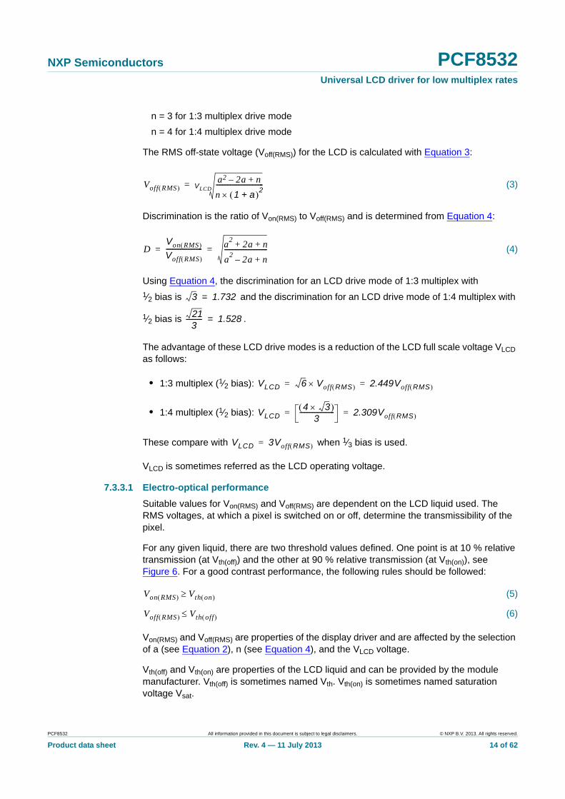
For any given liquid, there are two threshold values defined. One point is at 10 % relative transmission (at Vth(off)) and the other at 90 % relative transmission (at Vth(on)), see Figure 6. For a good contrast performance, the following rules should be followed:
(5)
(6)
Von(RMS) and Voff(RMS) are properties of the display driver and are affected by the selection of a (see Equation 2), n (see Equation 4), and the VLCD voltage.
Vth(off) and Vth(on) are properties of the LCD liquid and can be provided by the module manufacturer. Vth(off) is sometimes named Vth. Vth(on) is sometimes named saturation voltage Vsat.
Voff RMS a2 2a– n+
n 1 a+ 2------------------------------VLCD
=
DVon RMS
Voff RMS ----------------------- a
22a n+ +
a2
2a– n+---------------------------= =
3 1.732=
213
---------- 1.528=
VLCD 6 Voff RMS 2.449Voff RMS = =
VLCD4 3
3---------------------- 2.309Voff RMS = =
VLCD 3Voff RMS =
Von RMS Vth on
Voff RMS Vth off
PCF8532 All information provided in this document is subject to legal disclaimers. © NXP B.V. 2013. All rights reserved.
Product data sheet Rev. 4 — 11 July 2013 14 of 62
NXP Semiconductors PCF8532Universal LCD driver for low multiplex rates
It is important to match the module properties to those of the driver in order to achieve optimum performance.
Fig 6. Electro-optical characteristic: relative transmission curve of the liquid
VRMS [V]
100 %90 %
10 %
OFFSEGMENT
GREYSEGMENT
ONSEGMENT
Vth(off) Vth(on)
Rel
ativ
e Tr
ansm
issi
on
013aaa494
PCF8532 All information provided in this document is subject to legal disclaimers. © NXP B.V. 2013. All rights reserved.
Product data sheet Rev. 4 — 11 July 2013 15 of 62

NXP Semiconductors PCF8532Universal LCD driver for low multiplex rates
7.3.4 LCD drive mode waveforms
7.3.4.1 Static drive mode
The static LCD drive mode is used when a single backplane is provided in the LCD. Backplane and segment drive waveforms for this mode are shown in Figure 7.
Vstate1(t) = VSn(t) VBP0(t).
Von(RMS) = VLCD.
Vstate2(t) = V(Sn+1)(t) VBP0(t).
Voff(RMS) = 0 V.
Fig 7. Static drive mode waveforms
013aaa207
VSS
VLCD
VSS
VLCD
VSS
VLCD
VLCD
−VLCD
−VLCD
VLCD
state 1 0 V
BP0
Sn
Sn+1
state 2 0 V
(a) Waveforms at driver.
(b) Resultant waveformsat LCD segment.
LCD segments
state 1(on)
state 2(off)
Tfr
PCF8532 All information provided in this document is subject to legal disclaimers. © NXP B.V. 2013. All rights reserved.
Product data sheet Rev. 4 — 11 July 2013 16 of 62
NXP Semiconductors PCF8532Universal LCD driver for low multiplex rates
7.3.4.2 1:2 multiplex drive mode
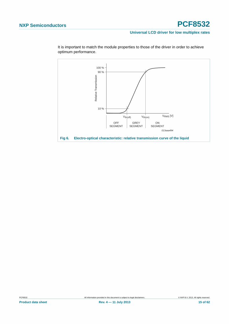
When two backplanes are provided in the LCD, the 1:2 multiplex mode applies. The PCF8532 allows the use of 1⁄2 bias or 1⁄3 bias in this mode as shown in Figure 8 and Figure 9.
Vstate1(t) = VSn(t) VBP0(t).
Von(RMS) = 0.791VLCD.
Vstate2(t) = VSn(t) VBP1(t).
Voff(RMS) = 0.354VLCD.
Fig 8. Waveforms for the 1:2 multiplex drive mode with 1⁄2 bias
013aaa208
state 1
BP0
(a) Waveforms at driver.
(b) Resultant waveformsat LCD segment.
LCD segments
state 2
BP1
state 2
state 1VSS
VLCD
VLCD/2
VSS
VSS
VLCD
VLCD
VSS
VLCD
VLCD
VLCD
0 V
0 V
VLCD/2
VLCD/2
VLCD/2
−VLCD
−VLCD
−VLCD/2
−VLCD/2
Sn
Sn+1
Tfr
PCF8532 All information provided in this document is subject to legal disclaimers. © NXP B.V. 2013. All rights reserved.
Product data sheet Rev. 4 — 11 July 2013 17 of 62

NXP Semiconductors PCF8532Universal LCD driver for low multiplex rates
Vstate1(t) = VSn(t) VBP0(t).
Von(RMS) = 0.745VLCD.
Vstate2(t) = VSn(t) VBP1(t).
Voff(RMS) = 0.333VLCD.
Fig 9. Waveforms for the 1:2 multiplex drive mode with 1⁄3 bias
013aaa209
state 1
BP0
(a) Waveforms at driver.
(b) Resultant waveformsat LCD segment.
LCD segments
state 2
BP1
state 1
state 2
VSS
VLCD
2VLCD/3
VLCD/3
VSS
VLCD
2VLCD/3
VLCD/3
VSS
VLCD
2VLCD/3
VLCD/3
0 V
VLCD
2VLCD/3
−2VLCD/3
VLCD/3
−VLCD/3
−VLCD
−VLCD
0 V
VLCD
2VLCD/3
−2VLCD/3
VLCD/3
−VLCD/3
Sn
Sn+1
Tfr
VSS
VLCD
2VLCD/3
VLCD/3
PCF8532 All information provided in this document is subject to legal disclaimers. © NXP B.V. 2013. All rights reserved.
Product data sheet Rev. 4 — 11 July 2013 18 of 62

NXP Semiconductors PCF8532Universal LCD driver for low multiplex rates
7.3.4.3 1:3 multiplex drive mode
When three backplanes are provided in the LCD, the 1:3 multiplex drive mode applies as shown in Figure 10.
Vstate1(t) = VSn(t) VBP0(t).
Von(RMS) = 0.638VLCD.
Vstate2(t) = VSn(t) VBP1(t).
Voff(RMS) = 0.333VLCD.
Fig 10. Waveforms for the 1:3 multiplex drive mode with 1⁄3 bias
013aaa210
state 1
BP0
(b) Resultant waveformsat LCD segment.
LCD segments
state 2
BP1
state 1
state 2
(a) Waveforms at driver.
BP2
Sn
Sn+1
Sn+2
Tfr
VSS
VLCD
2VLCD/3
VLCD/3
VSS
VLCD
2VLCD/3
VLCD/3
VSS
VLCD
2VLCD/3
VLCD/3
VSS
VLCD
2VLCD/3
VLCD/3
VSS
VLCD
2VLCD/3
VLCD/3
0 V
VLCD
2VLCD/3
−2VLCD/3
VLCD/3
−VLCD/3
−VLCD
0 V
VLCD
2VLCD/3
−2VLCD/3
VLCD/3
−VLCD/3
−VLCD
VSS
VLCD
2VLCD/3
VLCD/3
PCF8532 All information provided in this document is subject to legal disclaimers. © NXP B.V. 2013. All rights reserved.
Product data sheet Rev. 4 — 11 July 2013 19 of 62

NXP Semiconductors PCF8532Universal LCD driver for low multiplex rates
7.3.4.4 1:4 multiplex drive mode
When four backplanes are provided in the LCD, the 1:4 multiplex drive mode applies as shown in Figure 11.
Vstate1(t) = VSn(t) VBP0(t).
Von(RMS) = 0.577VLCD.
Vstate2(t) = VSn(t) VBP1(t).
Voff(RMS) = 0.333VLCD.
Fig 11. Waveforms for the 1:4 multiplex drive mode with 1⁄3 bias
013aaa211
state 1
BP0
(b) Resultant waveformsat LCD segment.
LCD segments
state 2BP1
state 1
state 2
BP2
(a) Waveforms at driver.
BP3
Sn
Sn+1
Sn+2
Sn+3
Tfr
VSS
VLCD2VLCD/3VLCD/3
VSS
VLCD2VLCD/3VLCD/3
VSS
VLCD2VLCD/3VLCD/3
VSS
VLCD2VLCD/3VLCD/3
VSS
VLCD2VLCD/3VLCD/3
VSS
VLCD2VLCD/3VLCD/3
VSS
VLCD2VLCD/3VLCD/3
0 V
VLCD2VLCD/3
-2VLCD/3
VLCD/3
-VLCD/3
-VLCD
0 V
VLCD2VLCD/3
-2VLCD/3
VLCD/3
-VLCD/3
-VLCD
VSS
VLCD2VLCD/3VLCD/3
PCF8532 All information provided in this document is subject to legal disclaimers. © NXP B.V. 2013. All rights reserved.
Product data sheet Rev. 4 — 11 July 2013 20 of 62
NXP Semiconductors PCF8532Universal LCD driver for low multiplex rates
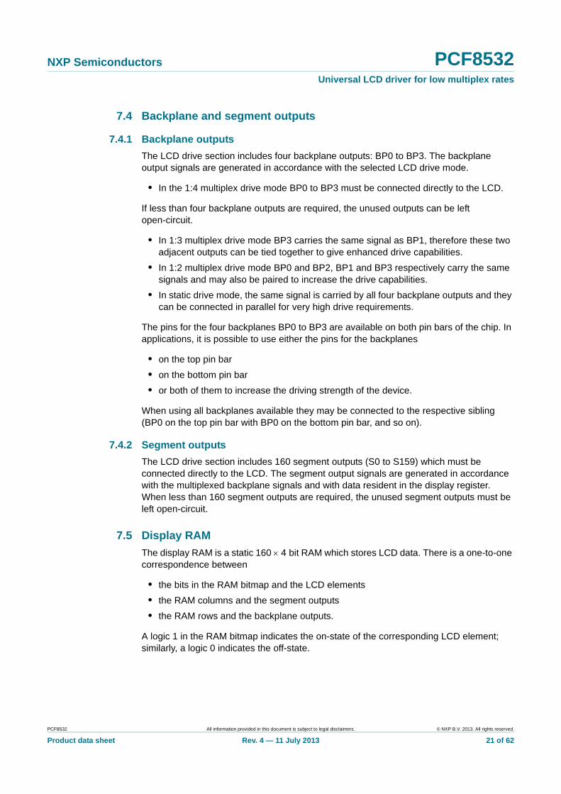
7.4 Backplane and segment outputs
7.4.1 Backplane outputs
The LCD drive section includes four backplane outputs: BP0 to BP3. The backplane output signals are generated in accordance with the selected LCD drive mode.
• In the 1:4 multiplex drive mode BP0 to BP3 must be connected directly to the LCD.
If less than four backplane outputs are required, the unused outputs can be left open-circuit.
• In 1:3 multiplex drive mode BP3 carries the same signal as BP1, therefore these two adjacent outputs can be tied together to give enhanced drive capabilities.
• In 1:2 multiplex drive mode BP0 and BP2, BP1 and BP3 respectively carry the same signals and may also be paired to increase the drive capabilities.
• In static drive mode, the same signal is carried by all four backplane outputs and they can be connected in parallel for very high drive requirements.
The pins for the four backplanes BP0 to BP3 are available on both pin bars of the chip. In applications, it is possible to use either the pins for the backplanes
• on the top pin bar
• on the bottom pin bar
• or both of them to increase the driving strength of the device.
When using all backplanes available they may be connected to the respective sibling (BP0 on the top pin bar with BP0 on the bottom pin bar, and so on).
7.4.2 Segment outputs
The LCD drive section includes 160 segment outputs (S0 to S159) which must be connected directly to the LCD. The segment output signals are generated in accordance with the multiplexed backplane signals and with data resident in the display register. When less than 160 segment outputs are required, the unused segment outputs must be left open-circuit.
7.5 Display RAM
The display RAM is a static 160 4 bit RAM which stores LCD data. There is a one-to-one correspondence between
• the bits in the RAM bitmap and the LCD elements
• the RAM columns and the segment outputs
• the RAM rows and the backplane outputs.
A logic 1 in the RAM bitmap indicates the on-state of the corresponding LCD element; similarly, a logic 0 indicates the off-state.
PCF8532 All information provided in this document is subject to legal disclaimers. © NXP B.V. 2013. All rights reserved.
Product data sheet Rev. 4 — 11 July 2013 21 of 62

NXP Semiconductors PCF8532Universal LCD driver for low multiplex rates
The display RAM bitmap, Figure 12, shows the rows 0 to 3 which correspond with the backplane outputs BP0 to BP3, and the columns 0 to 159 which correspond with the segment outputs S0 to S159. In multiplexed LCD applications the segment data of the first, second, third, and fourth row of the display RAM are time-multiplexed with BP0, BP1, BP2, and BP3 respectively.
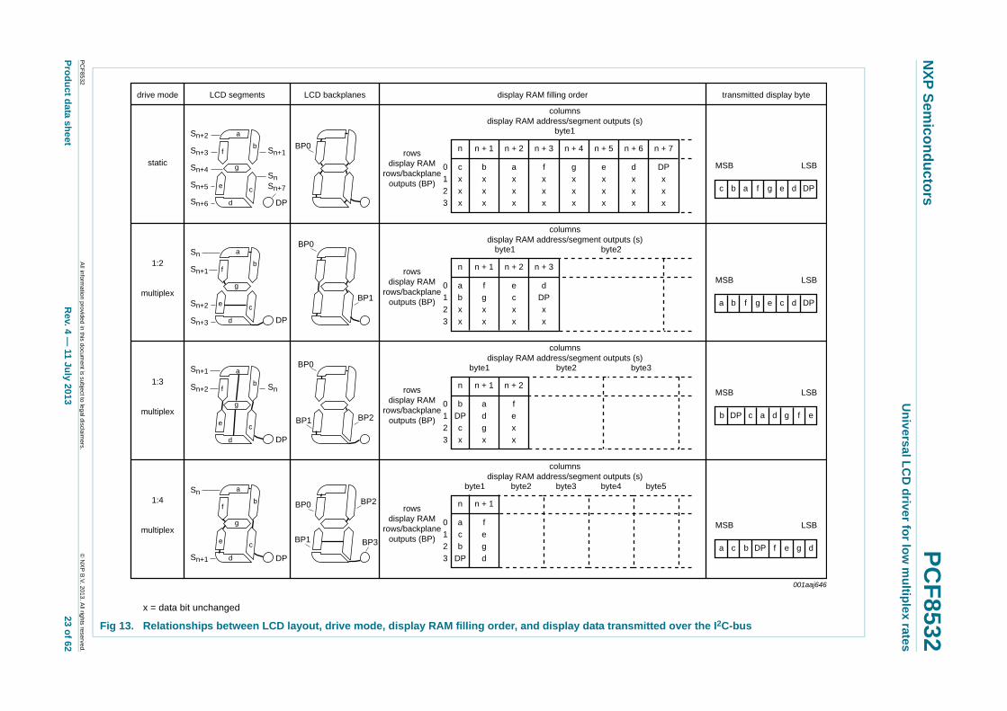
When display data is transmitted to the PCF8532, the received display bytes are stored in the display RAM in accordance with the selected LCD drive mode. The data is stored as it arrives and does not wait for the acknowledge cycle as with the commands. Depending on the current multiplex drive mode, data is stored singularly, in pairs, triples, or quadruples. To illustrate the filling order, an example of a 7-segment numeric display showing all drive modes is given in Figure 13. The RAM filling organization depicted applies equally to other LCD types.
The following applies to Figure 13:
• In static drive mode the eight transmitted data bits are placed in row 0 as 1 byte.
• In 1:2 multiplex drive mode the eight transmitted data bits are placed in pairs into row 0 and 1 as 2 successive 4-bit RAM words.
• In 1:3 multiplex drive mode the 8 bits are placed in triples into row 0, 1, and 2 as 3 successive 3-bit RAM words, with bit 3 of the third address left unchanged. It is not recommended to use this bit in a display because of the difficult addressing. This last bit may, if necessary, be controlled by an additional transfer to this address but care should be taken to avoid overwriting adjacent data because always full bytes are transmitted (see Section 7.5.3 on page 25).
• In 1:4 multiplex drive mode, the eight transmitted data bits are placed in quadruples into row 0, 1, 2, and 3 as 2 successive 4-bit RAM words.
The display RAM bitmap shows the direct relationship between the display RAM addresses and the segment outputs; and between the bits in a RAM word and the backplane outputs.
Fig 12. Display RAM bitmap
0
0
1
2
3
1 2 3 4 155 156 157 158 159
display RAM addresses/segment outputs (S)
display RAM rows/backplane outputs
(BP)
013aaa220
columns
rows
PCF8532 All information provided in this document is subject to legal disclaimers. © NXP B.V. 2013. All rights reserved.
Product data sheet Rev. 4 — 11 July 2013 22 of 62
xxxxxxxxxxxxxxxxxxxxx xxxxxxxxxxxxxxxxxxxxxxxxxx xxxxxxx x x x xxxxxxxxxxxxxxxxxxxxxxxxxxxxxx xxxxxxxxxxxxxxxxxxx xx xx xxxxx xxxxxxxxxxxxxxxxxxxxxxxxxxx xxxxxxxxxxxxxxxxxxx xxxxxx xxxxxxxxxxxxxxxxxxxxxxxxxxxxxxxxxxx xxxxxxxxxxxx x x xxxxxxxxxxxxxxxxxxxxx xxxxxxxxxxxxxxxxxxxxxxxxxxxxxx xxxxx xxxxxxxxxxxxxxxxxxxxxxxxxxxxxxxxxxxxxxxxxxxxxxxxxx xxxxxxxx xxxxxxxxxxxxxxxxxxxxxxxxx xxxxxxxxxxxxxxxxxxxx xxx
PC
F85
32
Pro
du
ct data sh
NX
P S
emico
nd
ucto
rsP
CF
8532U
niv
ers
al L
CD
drive
r for lo
w m
ultip
lex
rates
over the I2C-bus
001aaj646
a c b DP f e g d
MSB LSB
b DP c a d g f e
MSB LSB
a b f g e c d DP
MSB LSB
c b a f g e d DP
MSB LSB
drive mode LCD segments LCD backplanes display RAM filling order transmitted display byte
P
7
columnsdisplay RAM address/segment outputs (s)
All inform
ation provided
in this docum
ent is subject to leg
al disclaim
ers.©
NX
P B
.V. 2013. A
ll rights reserved.
eetR
ev. 4 — 11 Ju
ly 2013 23 o
f 62
x = data bit unchanged
Fig 13. Relationships between LCD layout, drive mode, display RAM filling order, and display data transmitted
static
1:2
multiplex
1:3
multiplex
1:4
multiplex
BP0
BP0
BP1
BP0
BP1 BP2
BP1
BP2
BP3
BP0
n
cxxx
0123
bxxx
axxx
fxxx
gxxx
exxx
dxxx
Dxxx
n + 1 n + 2 n + 3 n + 4 n + 5 n + 6 n +rowsdisplay RAM
rows/backplaneoutputs (BP)
byte1
n
abxx
0123
fgxx
ecxx
dDPxx
n + 1 n + 2 n + 3
byte1 byte2
rowsdisplay RAM
rows/backplaneoutputs (BP)
columnsdisplay RAM address/segment outputs (s)
n
bDPcx
0123
adgx
fexx
n + 1 n + 2
byte1 byte2 byte3
rowsdisplay RAM
rows/backplaneoutputs (BP)
columnsdisplay RAM address/segment outputs (s)
n + 1n
acb
DP
0123
fegd
byte1 byte2 byte3 byte4 byte5
rowsdisplay RAM
rows/backplaneoutputs (BP)
columnsdisplay RAM address/segment outputs (s)
Sn+2
Sn+3
Sn+1
Sn
DP
a
fb
g
e c
d
Sn+2
Sn+1
Sn+7
Sn
Sn+3
Sn+5
Sn+6
Sn+4
DP
a
fb
g
e c
d
Sn
Sn+1
Sn+2
DP
a
fb
g
e c
d
Sn+1
Sn
DP
a
fb
g
e c
d
NXP Semiconductors PCF8532Universal LCD driver for low multiplex rates
7.5.1 Data pointer
The addressing mechanism for the display RAM is realized using the data pointer. This allows the loading of an individual display data byte, or a series of display data bytes, into any location of the display RAM. The sequence commences with the initialization of the data pointer by the load-data-pointer command (see Table 7 on page 7 and Table 8 on page 7). Following this command, an arriving data byte is stored at the display RAM address indicated by the data pointer. The filling order is shown in Figure 13.
After each byte is stored, the content of the data pointer is automatically incremented by a value dependent on the selected LCD drive mode:
• In static drive mode by eight
• In 1:2 multiplex drive mode by four
• In 1:3 multiplex drive mode by three
• In 1:4 multiplex drive mode by two
If an I2C-bus data access is terminated early, then the state of the data pointer is unknown. The data pointer should be re-written before further RAM accesses.
7.5.2 Subaddress counter
The storage of display data is conditioned by the content of the subaddress counter. Storage is allowed only when the content of the subaddress counter matches with the hardware subaddress applied to A0 and A1. The subaddress counter value is defined by the device-select command (see Table 9 on page 7). If the content of the subaddress counter and the hardware subaddress do not match then data storage is inhibited but the data pointer is incremented as if data storage had taken place. The subaddress counter is also incremented when the data pointer overflows.
The storage arrangements described lead to extremely efficient data loading in cascaded applications. When a series of display bytes are sent to the display RAM, automatic wrap-over to the next PCF8532 occurs when the last RAM address is exceeded. Subaddressing across device boundaries is successful even if the change to the next device in the cascade occurs within a transmitted character.
The hardware subaddress must not be changed while the device is being accessed on the I2C-bus interface.
PCF8532 All information provided in this document is subject to legal disclaimers. © NXP B.V. 2013. All rights reserved.
Product data sheet Rev. 4 — 11 July 2013 24 of 62
NXP Semiconductors PCF8532Universal LCD driver for low multiplex rates
7.5.3 RAM writing in 1:3 multiplex drive mode
In 1:3 multiplex drive mode, the RAM is written as shown in Table 16 (see Figure 13 as well).
If the bit at position BP2/S2 would be written by a second byte transmitted, then the mapping of the segment bits would change as illustrated in Table 17.
In the case described in Table 17 the RAM has to be written entirely and BP2/S2, BP2/S5, BP2/S8, and so on, have to be connected to elements on the display. This can be achieved by a combination of writing and rewriting the RAM like follows:
• In the first write to the RAM, bits a7 to a0 are written
• The data-pointer (see Section 7.1.2 on page 7) has to be set to the address of bit a1
• In the second write, bits b7 to b0 are written, overwriting bits a1 and a0 with bits b7 and b6
• The data-pointer has to be set to the address of bit b1
• In the third write, bits c7 to c0 are written, overwriting bits b1 and b0 with bits c7 and c6
Depending on the method of writing to the RAM (standard or entire filling by rewriting), some elements remain unused or can be used, but it has to be considered in the module layout process as well as in the driver software design.
7.5.4 Bank selection
7.5.4.1 Output bank selector
The output bank selector (see Table 10 on page 8) selects one of the four rows per display RAM address for transfer to the display register. The actual row selected depends on the particular LCD drive mode in operation and on the instant in the multiplex sequence.
Table 16. Standard RAM filling in 1:3 multiplex drive modeAssumption: BP2/S2, BP2/S5, BP2/S8 etc. are not connected to any elements on the display.
Display RAM bits (rows)/ backplane outputs (BPn)
Display RAM addresses (columns)/segment outputs (Sn)
0 1 2 3 4 5 6 7 8 9 :
0 a7 a4 a1 b7 b4 b1 c7 c4 c1 d7 :
1 a6 a3 a0 b6 b3 b0 c6 c3 c0 d6 :
2 a5 a2 - b5 b2 - c5 c2 - d5 :
3 - - - - - - - - - - :
Table 17. Entire RAM filling by rewriting in 1:3 multiplex drive modeAssumption: BP2/S2, BP2/S5, BP2/S8 etc. are connected to elements on the display.
Display RAM bits (rows)/ backplane outputs (BPn)
Display RAM addresses (columns)/segment outputs (Sn)
0 1 2 3 4 5 6 7 8 9 :
0 a7 a4 a1/b7 b4 b1/c7 c4 c1/d7 d4 d1/e7 e4 :
1 a6 a3 a0/b6 b3 b0/c6 c3 c0/d6 d3 d0/e6 e3 :
2 a5 a2 b5 b2 c5 c2 d5 d2 e5 e2 :
3 - - - - - - - - - - :
PCF8532 All information provided in this document is subject to legal disclaimers. © NXP B.V. 2013. All rights reserved.
Product data sheet Rev. 4 — 11 July 2013 25 of 62

NXP Semiconductors PCF8532Universal LCD driver for low multiplex rates
• In 1:4 multiplex mode, all RAM addresses of row 0 are selected, followed by the contents of row 1, row 2, and then row 3
• In 1:3 multiplex mode, rows 0, 1, and 2 are selected sequentially
• In 1:2 multiplex mode, rows 0 and 1 are selected
• In static mode, row 0 is selected
7.5.4.2 Input bank selector
The input bank selector loads display data into the display RAM in accordance with the selected LCD drive configuration. Display data can be loaded by using the bank-select command (see Table 10). The input bank selector functions independently to the output bank selector.
7.5.4.3 RAM bank switching
The PCF8532 includes a RAM bank switching feature in the static and 1:2 multiplex drive modes. A bank can be thought of as one RAM row or a collection of RAM rows (see Figure 14). The RAM bank switching gives the provision for preparing display information in an alternative bank and to be able to switch to it once it is complete.
There are two banks; bank 0 and bank 1. Figure 14 shows the location of these banks relative to the RAM map. Input and output banks can be set independently from one another with the Bank-select command (see Table 10 on page 8). Figure 15 shows the concept.
Fig 14. RAM banks in static and multiplex driving mode 1:2
PCF8532 All information provided in this document is subject to legal disclaimers. © NXP B.V. 2013. All rights reserved.
Product data sheet Rev. 4 — 11 July 2013 26 of 62

NXP Semiconductors PCF8532Universal LCD driver for low multiplex rates
In the static drive mode, the bank-select command may request the contents of row 2 to be selected for display instead of the contents of row 0. In the 1:2 multiplex mode, the contents of rows 2 and 3 may be selected instead of rows 0 and 1. This gives the provision for preparing display information in an alternative bank and to be able to switch to it once it is assembled.
In Figure 16 an example is shown for 1:2 multiplex drive mode where the displayed data is read from the first two rows of the memory (bank 0), while the transmitted data is stored in the second two rows of the memory (bank 1).
Fig 15. Bank selection
Fig 16. Example of the Bank-select command with multiplex drive mode 1:2
PCF8532 All information provided in this document is subject to legal disclaimers. © NXP B.V. 2013. All rights reserved.
Product data sheet Rev. 4 — 11 July 2013 27 of 62

NXP Semiconductors PCF8532Universal LCD driver for low multiplex rates
8. Characteristics of the I2C-bus
The I2C-bus is for bidirectional, two-line communication between different ICs or modules. The two lines are a Serial DAta line (SDA) and a Serial CLock line (SCL). Both lines must be connected to a positive supply via a pull-up resistor when connected to the output stages of a device. Data transfer may be initiated only when the bus is not busy.
By connecting pin SDAACK to pin SDA on the PCF8532, the SDA line becomes fully I2C-bus compatible. In COG applications where the track resistance from the SDAACK pin to the system SDA line can be significant, possibly a voltage divider is generated by the bus pull-up resistor and the Indium Tin Oxide (ITO) track resistance. As a consequence, it may be possible that the acknowledge generated by the PCF8532 cannot be interpreted as logic 0 by the master. In COG applications where the acknowledge cycle is required, it is therefore necessary to minimize the track resistance from the SDAACK pin to the system SDA line to guarantee a valid LOW level (see Section 14.2 on page 41).
By separating the acknowledge output from the serial data line (having the SDAACK open circuit) design efforts to generate a valid acknowledge level can be avoided. However, in that case the I2C-bus master has to be set up in such a way that it ignores the acknowledge cycle.2
The following definition assumes that SDA and SDAACK are connected and refers to the pair as SDA.
8.1 Bit transfer
One data bit is transferred during each clock pulse. The data on the SDA line must remain stable during the HIGH period of the clock pulse as changes in the data line at this time are interpreted as a control signal (see Figure 17).
8.1.1 START and STOP conditions
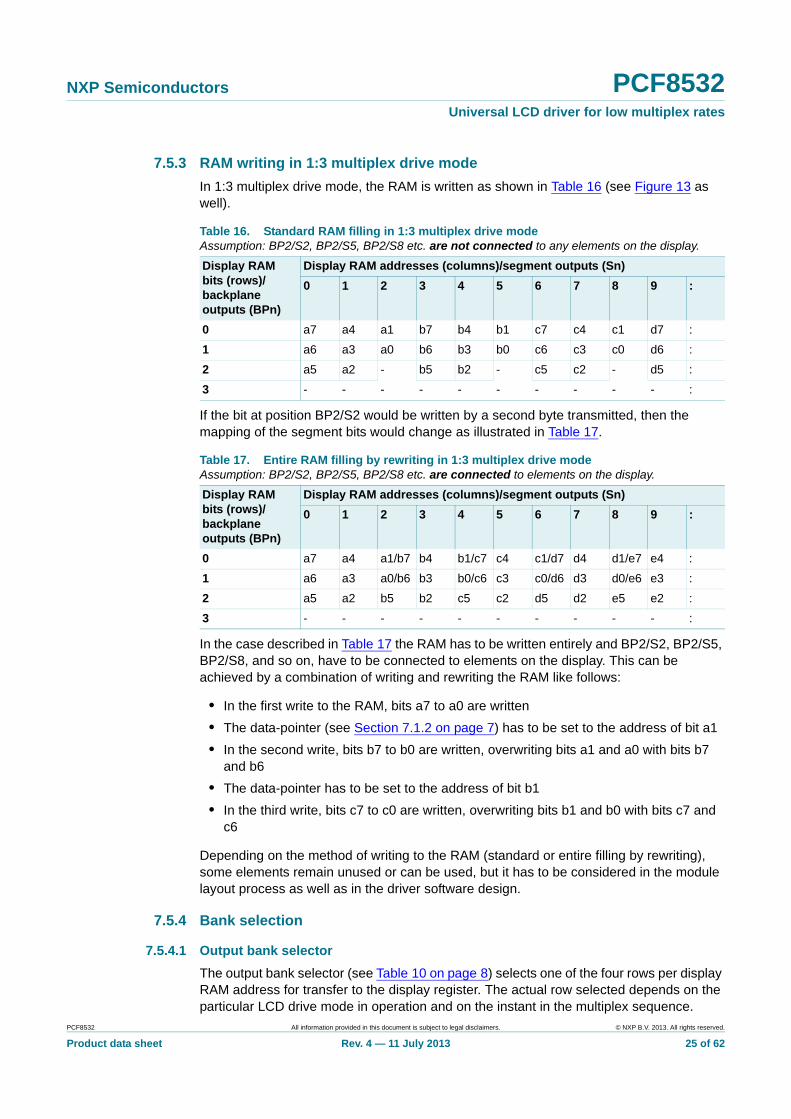
Both data and clock lines remain HIGH when the bus is not busy. A HIGH-to-LOW change of the data line, while the clock is HIGH is defined as the START condition (S). A LOW-to-HIGH change of the data line while the clock is HIGH is defined as the STOP condition (P). The START and STOP conditions are shown in Figure 18.
2. For further information, please consider the NXP application note: Ref. 1 “AN10170”.
Fig 17. Bit transfer
mba607
data linestable;
data valid
changeof dataallowed
SDA
SCL
PCF8532 All information provided in this document is subject to legal disclaimers. © NXP B.V. 2013. All rights reserved.
Product data sheet Rev. 4 — 11 July 2013 28 of 62
NXP Semiconductors PCF8532Universal LCD driver for low multiplex rates
8.2 System configuration
A device generating a message is a transmitter; a device receiving a message is the receiver. The device that controls the message is the master and the devices which are controlled by the master are the slaves. The system configuration is shown in Figure 19.
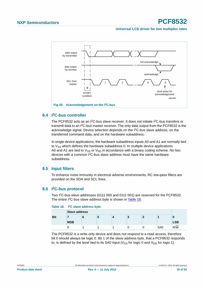
8.3 Acknowledge
The number of data bytes transferred between the START and STOP conditions from transmitter to receiver is unlimited. Each byte of 8 bits is followed by an acknowledge cycle.
• A slave receiver which is addressed must generate an acknowledge after the reception of each byte.
• Also a master receiver must generate an acknowledge after the reception of each byte that has been clocked out of the slave transmitter.
• The device that acknowledges must pull-down the SDA line during the acknowledge clock pulse, so that the SDA line is stable LOW during the HIGH period of the acknowledge related clock pulse (set-up and hold times must be considered).
• A master receiver must signal an end of data to the transmitter by not generating an acknowledge on the last byte that has been clocked out of the slave. In this event, the transmitter must leave the data line HIGH to enable the master to generate a STOP condition.
Acknowledgement on the I2C-bus is shown in Figure 20.
Fig 18. Definition of START and STOP conditions
mbc622
SDA
SCLP
STOP condition
SDA
SCLS
START condition
Fig 19. System configuration
mga807
SDA
SCL
MASTERTRANSMITTER/
RECEIVER
MASTERTRANSMITTER
SLAVETRANSMITTER/
RECEIVER
SLAVERECEIVER
MASTERTRANSMITTER/
RECEIVER
PCF8532 All information provided in this document is subject to legal disclaimers. © NXP B.V. 2013. All rights reserved.
Product data sheet Rev. 4 — 11 July 2013 29 of 62
NXP Semiconductors PCF8532Universal LCD driver for low multiplex rates
8.4 I2C-bus controller
The PCF8532 acts as an I2C-bus slave receiver. It does not initiate I2C-bus transfers or transmit data to an I2C-bus master receiver. The only data output from the PCF8532 is the acknowledge signal. Device selection depends on the I2C-bus slave address, on the transferred command data, and on the hardware subaddress.
In single device applications, the hardware subaddress inputs A0 and A1 are normally tied to VSS which defines the hardware subaddress 0. In multiple device applications A0 and A1 are tied to VSS or VDD in accordance with a binary coding scheme. No two devices with a common I2C-bus slave address must have the same hardware subaddress.
8.5 Input filters
To enhance noise immunity in electrical adverse environments, RC low-pass filters are provided on the SDA and SCL lines.
8.6 I2C-bus protocol
Two I2C-bus slave addresses (0111 000 and 0111 001) are reserved for the PCF8532. The entire I2C-bus slave address byte is shown in Table 18.
The PCF8532 is a write-only device and does not respond to a read access, therefore bit 0 should always be logic 0. Bit 1 of the slave address byte, that a PCF8532 responds to, is defined by the level tied to its SA0 input (VSS for logic 0 and VDD for logic 1).
Fig 20. Acknowledgement on the I2C-bus
mbc602
S
STARTcondition
9821
clock pulse foracknowledgement
not acknowledge
acknowledge
data outputby transmitter
data outputby receiver
SCL frommaster
Table 18. I2C slave address byte
Slave address
Bit 7 6 5 4 3 2 1 0
MSB LSB
0 1 1 1 0 0 SA0 R/W
PCF8532 All information provided in this document is subject to legal disclaimers. © NXP B.V. 2013. All rights reserved.
Product data sheet Rev. 4 — 11 July 2013 30 of 62

NXP Semiconductors PCF8532Universal LCD driver for low multiplex rates
Having two reserved slave addresses allows the following on the same I2C-bus:
• Up to 8 PCF8532 on the same I2C-bus for very large LCD applications
• The use of two types of LCD multiplex drive modes on the same I2C-bus
The I2C-bus protocol is shown in Figure 21. The sequence is initiated with a START condition (S) from the I2C-bus master which is followed by one of two possible PCF8532 slave addresses available. All PCF8532 with the corresponding SA0 level acknowledge in parallel to the slave address, but all PCF8532 with the alternative SA0 level ignore the whole I2C-bus transfer.
After acknowledgement, a control byte follows which defines if the next byte is RAM or command information.
Fig 21. I2C-bus protocol
EXAMPLESa) transmit two bytes of RAM data
mgl752
SA0
S 0 1 1 1 0 00
control byteslave address RAM/command byte
RAM DATA
MSB
LSB
A A P
R/W = 0
SA0
S 0 1 1 1 0 0 0 10 A A A PRAM DATA A
b) transmit two command bytes
COMMANDSA0
S 0 1 1 1 0 0 1 00 A A A PCOMMAND AA
c) transmit one command byte and two RAM date bytes
COMMANDSA0
S 0 1 1 1 0 0 1 0
0 0
0 10 A A A PRAM DATA A RAM DATA AA
CO
RS
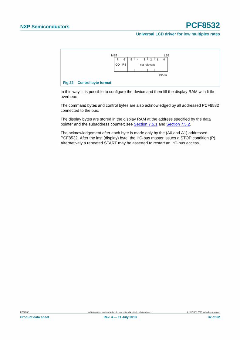
Table 19. Control byte description
Bit Symbol Value Description
7 CO continue bit
0 last control byte
1 control bytes continue
6 RS register selection
0 command register
1 data register
5 to 0 - - not relevant
PCF8532 All information provided in this document is subject to legal disclaimers. © NXP B.V. 2013. All rights reserved.
Product data sheet Rev. 4 — 11 July 2013 31 of 62
NXP Semiconductors PCF8532Universal LCD driver for low multiplex rates
In this way, it is possible to configure the device and then fill the display RAM with little overhead.
The command bytes and control bytes are also acknowledged by all addressed PCF8532 connected to the bus.
The display bytes are stored in the display RAM at the address specified by the data pointer and the subaddress counter; see Section 7.5.1 and Section 7.5.2.
The acknowledgement after each byte is made only by the (A0 and A1) addressed PCF8532. After the last (display) byte, the I2C-bus master issues a STOP condition (P). Alternatively a repeated START may be asserted to restart an I2C-bus access.
Fig 22. Control byte format
mgl753
not relevantCO
7 6 5 4 3 2 1 0
RS
MSB LSB
PCF8532 All information provided in this document is subject to legal disclaimers. © NXP B.V. 2013. All rights reserved.
Product data sheet Rev. 4 — 11 July 2013 32 of 62

NXP Semiconductors PCF8532Universal LCD driver for low multiplex rates
9. Internal circuitry
Fig 23. Device protection diagram
SA0
VDD VDD
VSS VSS
VLCD
VSS
SDA
001aah856
VSS
SDAACK
VSS
SCL
VSS
CLK
VDD
VSS
OSC
VDD
VSS
SYNC
VDD
VSS
A0, A1
VDD
VSS
BP0 to BP3
VLCD
VSS
S0 to S159
VLCD
VSS
T3
VSS
T1, T2
VDD
VSS
PCF8532 All information provided in this document is subject to legal disclaimers. © NXP B.V. 2013. All rights reserved.
Product data sheet Rev. 4 — 11 July 2013 33 of 62

NXP Semiconductors PCF8532Universal LCD driver for low multiplex rates
10. Safety notes
CAUTION
This device is sensitive to ElectroStatic Discharge (ESD). Observe precautions for handling electrostatic sensitive devices.
Such precautions are described in the ANSI/ESD S20.20, IEC/ST 61340-5, JESD625-A or equivalent standards.
CAUTION
Static voltages across the liquid crystal display can build up when the LCD supply voltage (VLCD) is on while the IC supply voltage (VDD) is off, or vice versa. This may cause unwanted display artifacts. To avoid such artifacts, VLCD and VDD must be applied or removed together.
CAUTION
Semiconductors are light sensitive. Exposure to light sources can cause the IC to malfunction. The IC must be protected against light. The protection must be applied to all sides of the IC.
PCF8532 All information provided in this document is subject to legal disclaimers. © NXP B.V. 2013. All rights reserved.
Product data sheet Rev. 4 — 11 July 2013 34 of 62

NXP Semiconductors PCF8532Universal LCD driver for low multiplex rates
11. Limiting values
[1] Stresses above these values listed may cause permanent damage to the device.
[2] Pass level; Human Body Model (HBM) according to Ref. 6 “JESD22-A114”.
[3] Pass level; Machine Model (MM), according to Ref. 7 “JESD22-A115”.
[4] Pass level; latch-up testing, according to Ref. 8 “JESD78” at maximum ambient temperature (Tamb(max)).
[5] According to the store and transport requirements (see Ref. 11 “UM10569”) the devices have to be stored at a temperature of +8 C to +45 C and a humidity of 25 % to 75 %.
Table 20. Limiting valuesIn accordance with the Absolute Maximum Rating System (IEC 60134).[1]
Symbol Parameter Conditions Min Max Unit
VDD supply voltage 0.5 +6.5 V
IDD supply current 50 +50 mA
VLCD LCD supply voltage 0.5 +9.0 V
IDD(LCD) LCD supply current 50 +50 mA
Vi input voltage on pins CLK, SYNC, SA0, OSC, SDA, SCL, A0, A1, T1, T2, and T3
0.5 +6.5 V
II input current 10 +10 mA
VO output voltage on pins S0 to S159 and BP0 to BP3
0.5 +7.5 V
on pins SDAACK, CLK, SYNC
0.5 +6.5 V
IO output current 10 +10 mA
ISS ground supply current 50 +50 mA
Ptot total power dissipation - 400 mW
P/out power dissipation per output - 100 mW
VESD electrostatic discharge voltage
HBM [2] - 4500 V
MM [3] - 250 V
Ilu latch-up current [4] - 200 mA
Tstg storage temperature [5] 65 +150 C
Tamb ambient temperature operating device 40 +85 C
PCF8532 All information provided in this document is subject to legal disclaimers. © NXP B.V. 2013. All rights reserved.
Product data sheet Rev. 4 — 11 July 2013 35 of 62
NXP Semiconductors PCF8532Universal LCD driver for low multiplex rates
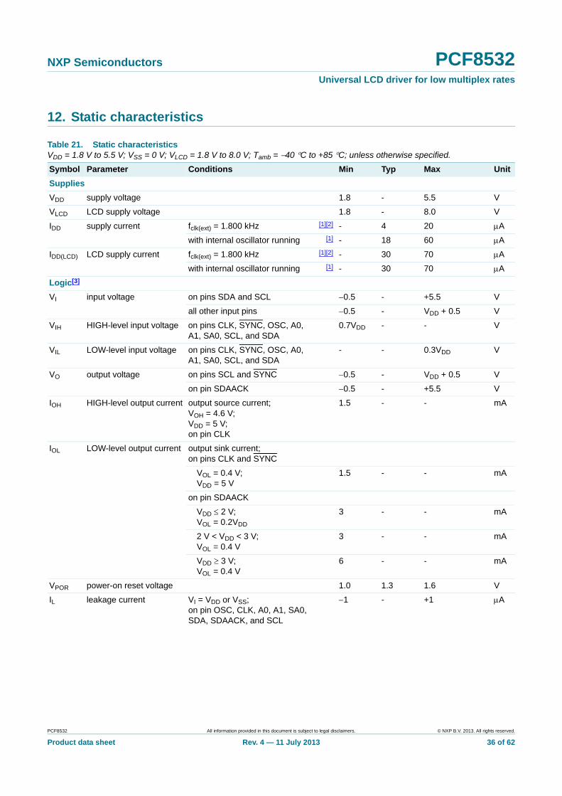
12. Static characteristics
Table 21. Static characteristicsVDD = 1.8 V to 5.5 V; VSS = 0 V; VLCD = 1.8 V to 8.0 V; Tamb = 40 C to +85 C; unless otherwise specified.
Symbol Parameter Conditions Min Typ Max Unit
Supplies
VDD supply voltage 1.8 - 5.5 V
VLCD LCD supply voltage 1.8 - 8.0 V
IDD supply current fclk(ext) = 1.800 kHz [1][2] - 4 20 A
with internal oscillator running [1] - 18 60 A
IDD(LCD) LCD supply current fclk(ext) = 1.800 kHz [1][2] - 30 70 A
with internal oscillator running [1] - 30 70 A
Logic[3]
VI input voltage on pins SDA and SCL 0.5 - +5.5 V
all other input pins 0.5 - VDD + 0.5 V
VIH HIGH-level input voltage on pins CLK, SYNC, OSC, A0, A1, SA0, SCL, and SDA
0.7VDD - - V
VIL LOW-level input voltage on pins CLK, SYNC, OSC, A0, A1, SA0, SCL, and SDA
- - 0.3VDD V
VO output voltage on pins SCL and SYNC 0.5 - VDD + 0.5 V
on pin SDAACK 0.5 - +5.5 V
IOH HIGH-level output current output source current;VOH = 4.6 V; VDD = 5 V; on pin CLK
1.5 - - mA
IOL LOW-level output current output sink current;on pins CLK and SYNC
VOL = 0.4 V; VDD = 5 V
1.5 - - mA
on pin SDAACK
VDD 2 V; VOL = 0.2VDD
3 - - mA
2 V < VDD < 3 V; VOL = 0.4 V
3 - - mA
VDD 3 V; VOL = 0.4 V
6 - - mA
VPOR power-on reset voltage 1.0 1.3 1.6 V
IL leakage current VI = VDD or VSS; on pin OSC, CLK, A0, A1, SA0, SDA, SDAACK, and SCL
1 - +1 A
PCF8532 All information provided in this document is subject to legal disclaimers. © NXP B.V. 2013. All rights reserved.
Product data sheet Rev. 4 — 11 July 2013 36 of 62

NXP Semiconductors PCF8532Universal LCD driver for low multiplex rates
[1] LCD outputs are open-circuit; inputs at VSS or VDD; I2C-bus inactive; VLCD = 8.0 V, VDD = 5.0 V and RAM written with all logic 1.
[2] External clock with 50 % duty factor.
[3] The I2C-bus interface of PCF8532 is 5 V tolerant.
[4] Variation between any 2 backplanes on a given voltage level; static measured.
[5] Variation between any 2 segments on a given voltage level; static measured.
LCD outputs
VO output voltage variation on pins BP0 to BP3 and S0 to S159
[4][5] 30 - +30 mV
RO output resistance VLCD = 5 V
on pins BP0 to BP3 - 1.5 5 k
on pins S0 to S159 - 2.0 5 k
Table 21. Static characteristics …continuedVDD = 1.8 V to 5.5 V; VSS = 0 V; VLCD = 1.8 V to 8.0 V; Tamb = 40 C to +85 C; unless otherwise specified.
Symbol Parameter Conditions Min Typ Max Unit
Tamb = 25 C; MUX 1:4; all RAM written with logic 1; no display connected; external clock with fclk(ext) = 1.800 kHz.
Fig 24. IDD(LCD) (typical) with respect to VLCD
VLCD (V)1 9753
001aaj497
20
10
30
40
IDD(LCD)(μA)
0
PCF8532 All information provided in this document is subject to legal disclaimers. © NXP B.V. 2013. All rights reserved.
Product data sheet Rev. 4 — 11 July 2013 37 of 62
NXP Semiconductors PCF8532Universal LCD driver for low multiplex rates
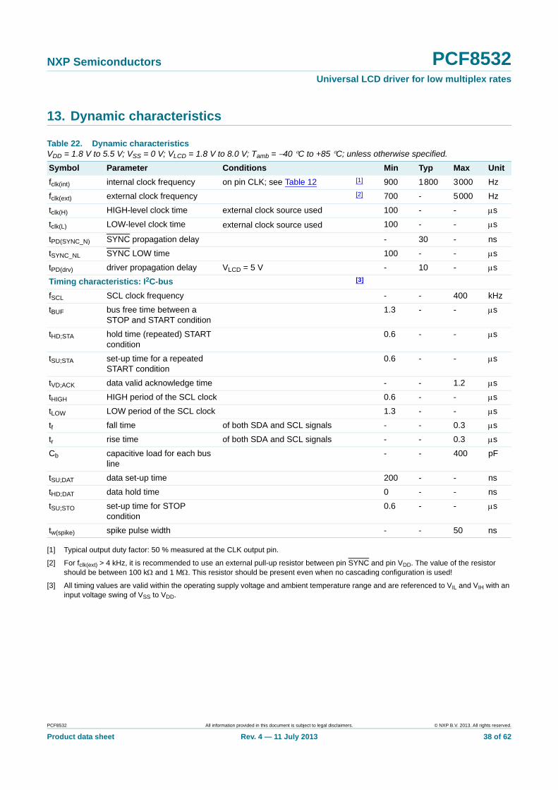
13. Dynamic characteristics
[1] Typical output duty factor: 50 % measured at the CLK output pin.
[2] For fclk(ext) > 4 kHz, it is recommended to use an external pull-up resistor between pin SYNC and pin VDD. The value of the resistor should be between 100 k and 1 M. This resistor should be present even when no cascading configuration is used!
[3] All timing values are valid within the operating supply voltage and ambient temperature range and are referenced to VIL and VIH with an input voltage swing of VSS to VDD.
Table 22. Dynamic characteristicsVDD = 1.8 V to 5.5 V; VSS = 0 V; VLCD = 1.8 V to 8.0 V; Tamb = 40 C to +85 C; unless otherwise specified.
Symbol Parameter Conditions Min Typ Max Unit
fclk(int) internal clock frequency on pin CLK; see Table 12 [1] 900 1800 3000 Hz
fclk(ext) external clock frequency [2] 700 - 5000 Hz
tclk(H) HIGH-level clock time external clock source used 100 - - s
tclk(L) LOW-level clock time external clock source used 100 - - s
tPD(SYNC_N) SYNC propagation delay - 30 - ns
tSYNC_NL SYNC LOW time 100 - - s
tPD(drv) driver propagation delay VLCD = 5 V - 10 - s
Timing characteristics: I2C-bus [3]
fSCL SCL clock frequency - - 400 kHz
tBUF bus free time between a STOP and START condition
1.3 - - s
tHD;STA hold time (repeated) START condition
0.6 - - s
tSU;STA set-up time for a repeated START condition
0.6 - - s
tVD;ACK data valid acknowledge time - - 1.2 s
tHIGH HIGH period of the SCL clock 0.6 - - s
tLOW LOW period of the SCL clock 1.3 - - s
tf fall time of both SDA and SCL signals - - 0.3 s
tr rise time of both SDA and SCL signals - - 0.3 s
Cb capacitive load for each bus line
- - 400 pF
tSU;DAT data set-up time 200 - - ns
tHD;DAT data hold time 0 - - ns
tSU;STO set-up time for STOP condition
0.6 - - s
tw(spike) spike pulse width - - 50 ns
PCF8532 All information provided in this document is subject to legal disclaimers. © NXP B.V. 2013. All rights reserved.
Product data sheet Rev. 4 — 11 July 2013 38 of 62

NXP Semiconductors PCF8532Universal LCD driver for low multiplex rates
Fig 25. Driver timing waveforms
Fig 26. I2C-bus timing waveforms
001aah848tPD(drv)
tSYNC_NL
tPD(SYNC_N)
CLK
SYNC
BP0 to BP3,and S0 to S159
tclk(H) tclk(L)
1 / fCLK
0.7 VDD
0.3 VDD
0.7 VDD
0.3 VDD
0.5 V
(VDD = 5 V)
0.5 V
SDA
001aah850
SDA
SCL
tSU;STA tSU;STO
tHD;STA
tBUF tLOW
tHD;DAT tHIGHtr
tf
tSU;DAT
tVD;ACK
PCF8532 All information provided in this document is subject to legal disclaimers. © NXP B.V. 2013. All rights reserved.
Product data sheet Rev. 4 — 11 July 2013 39 of 62

NXP Semiconductors PCF8532Universal LCD driver for low multiplex rates
14. Application information
14.1 Pull-up resistor sizing on I2C-bus
14.1.1 Max value of pull-up resistor
The bus capacitance (Cb) is the total capacitance of wire, connections, and pins. This capacitance on pin SDA limits the maximum value of the pull-up resistor (RPU) due to the specified rise time.
According to the I2C-bus specification the rise time (tr) is defined between the VDD-related input threshold of VIL = 0.3VDD and VIH = 0.7VDD. The value for tr(max) is 300 ns.
tr is calculated with Equation 7:
(7)
whereas t1 and t2 are the time since the charging started. The values for t1 and t2 are derivatives of the functions V(t1) and V(t2):
(8)
(9)
with the results of
(10)
(11)
(12)
RPU(max) is a function of the rise time (tr) and the bus capacitance (Cb) and is calculated with Equation 13:
(13)
14.1.2 Min value of pull-up resistor
The supply voltage limits the minimum value of resistor RPU due to the specified minimum sink current (see value of IOL on pin SDAACK in Table 21 on page 36). RPU(min) as a function of VDD is calculated with Equation 14:
(14)
The designer now has the minimum and maximum value of RPU. The values for RPU(max) and RPU(min) are shown in Figure 27 and Figure 28.
tr t2 t1–=
V t1 0.3VDD VDD 1 e-t1 RPUCb
– = =
V t2 0.7VDD VDD 1 e-t2 RPUCb
– = =
t1 R– PUCb ln 0.7( )=
t2 R– PUCb ln 0.3( )=
tr R– PUCb ln 0.3( ) RPUCb ln 0.7( )+=
RPU max tr
0.8473Cb----------------------- 300 10 9–
0.8473Cb--------------------------==
RPU min VDD VOL–
IOL--------------------------=
PCF8532 All information provided in this document is subject to legal disclaimers. © NXP B.V. 2013. All rights reserved.
Product data sheet Rev. 4 — 11 July 2013 40 of 62

NXP Semiconductors PCF8532Universal LCD driver for low multiplex rates
14.2 ITO track resistance
If an application requires to have a low VDD supply voltage compared to the VLCD supply voltage, it is recommended to increase the ITO resistance on the VLCD supply track in order to reduce the noise induced on the VSS line when display is enabled. A low VDD voltage supply and noise peaks on VSS induced by display activities may introduce disturbances into the I2C communication with the microcontroller.
Figure 29 shows that, when the ITO resistance of the VSS pin has a certain value, it is indicated to have a higher ITO resistance on the VLCD track, especially if VLCD (for example, 9 V) is sharply higher than VDD (for example, 1.8 V). With a higher ITO resistance on the VLCD track, the noise spikes induced to the VSS of the PCF8532 are getting smaller and the functionality is less affected.
Fig 27. Values for RPU(max)
Fig 28. Values for RPU(min)
Cb (pF)20 500340180100 42026060 380220140 460300
001aak441
2
4
6
0
1
3
5
RPU(max)(kΩ)
VDD (V)1 653 421.5 5.53.5 4.52.5
001aak440
2
4
6
1
3
5
RPU(min)(kΩ)
0
PCF8532 All information provided in this document is subject to legal disclaimers. © NXP B.V. 2013. All rights reserved.
Product data sheet Rev. 4 — 11 July 2013 41 of 62

NXP Semiconductors PCF8532Universal LCD driver for low multiplex rates
Tamb = 25 C; RITO(VSS) = 25 ; RITO(VDD) = 50 .
(1) RITO(VLCD) = 50 .
(2) RITO(VLCD) = 100 .
(3) RITO(VLCD) = 150 .
a. Operating range of the PCF8532 with RITO(VSS) = 25
Tamb = 25 C; RITO(VSS) = 50 ; RITO(VDD) = 50 .
(1) RITO(VLCD) = 50 .
(2) RITO(VLCD) = 75 .
(3) RITO(VLCD) = 100 .
(4) RITO(VLCD) = 150 .
(5) RITO(VLCD) = 200 .
(6) RITO(VLCD) = 300 .
b. Operating range of the PCF8532 with RITO(VSS) = 50
Fig 29. Operating range of the PCF8532 with respect to the ITO track resistance
PCF8532 All information provided in this document is subject to legal disclaimers. © NXP B.V. 2013. All rights reserved.
Product data sheet Rev. 4 — 11 July 2013 42 of 62

NXP Semiconductors PCF8532Universal LCD driver for low multiplex rates
14.3 SDA and SDAACK configuration
The Serial DAta Line (SDA) and the I2C-bus acknowledge line (SDAACK) are split. Both lines can be connected together to facilitate a single-line SDA.
14.4 Cascaded operation
In large display configurations, up to 8 PCF8532 can be distinguished on the same I2C-bus by using the 2-bit hardware subaddress (A0 and A1) and the programmable I2C-bus slave address (SA0).
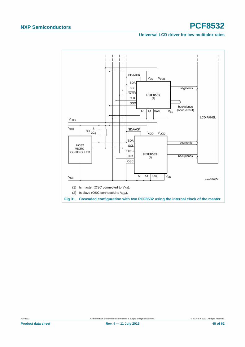
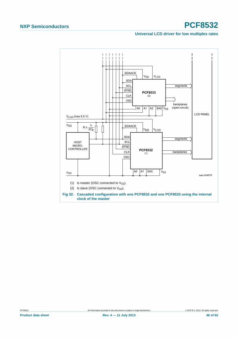
When cascaded PCF8532 are synchronized, they can share the backplane signals from one of the devices in the cascade. Such an arrangement is cost-effective in large LCD applications since the backplane outputs of only one device need to be through-plated to the backplane electrodes of the display. The other PCF8532 of the cascade contribute additional segment outputs but their backplane outputs are left open-circuit (see Figure 31 on page 45).
For display sizes that are not multiple of 640 elements, a mixed cascaded system can be considered containing only devices like PCF8532 and PCA85133. Depending on the application, one must take care of the software commands compatibility and pin connection compatibility.
The SYNC line is provided to maintain the correct synchronization between all cascaded PCF8532. This synchronization is guaranteed after the Power-On Reset (POR). The only time that SYNC is likely to be needed is if synchronization is accidentally lost (for example, by noise in adverse electrical environments, or by the definition of a multiplex mode when PCF8532 with different SA0 levels are cascaded). SYNC is organized as an input/output pin; the output selection being realized as an open-drain driver with an internal pull-up resistor. A PCF8532 asserts the SYNC line at the onset of its last active backplane signal and monitors the SYNC line at all other times. Should synchronization in
Fig 30. SDA, SDAACK configurations
013aaa111
SDA
two wire mode
SDAACK
SDA
single wire mode
SDAACK
Table 23. Addressing cascaded PCF8532
Cluster Bit SA0 Pin A1 Pin A0 Device
1 0 0 0 0
0 1 1
1 0 2
1 1 3
2 1 0 0 4
0 1 5
1 0 6
1 1 7
PCF8532 All information provided in this document is subject to legal disclaimers. © NXP B.V. 2013. All rights reserved.
Product data sheet Rev. 4 — 11 July 2013 43 of 62

NXP Semiconductors PCF8532Universal LCD driver for low multiplex rates
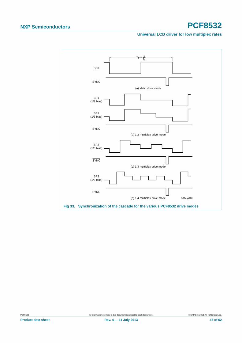
the cascade be lost, it is restored by the first PCF8532 to assert SYNC. The timing relationship between the backplane waveforms and the SYNC signal for the various drive modes of the PCF8532 are shown in Figure 33 on page 47.
When using an external clock signal with high frequencies (fclk(ext) > 4 kHz), it is recommended to have an external pull-up resistor between pin SYNC and pin VDD (see Table 22 on page 38). This resistor should be present even when no cascading configuration is used! When using it in a cascaded configuration, care must be taken not to route the SYNC signal to close to noisy signals.
The contact resistance between the SYNC pads of cascaded devices must be controlled. If the resistance is too high, the device is not able to synchronize properly. This is particularly applicable to COG applications. Table 24 shows the limiting values for contact resistance.
In the cascaded applications, the OSC pin of the PCF8532 with subaddress 0 is connected to VSS so that this device uses its internal clock to generate a clock signal at the CLK pin. The other PCF8532 devices are having the OSC pin connected to VDD, meaning that these devices are ready to receive external clock, the signal being provided by the device with subaddress 0.
If the master is providing the clock signal to the slave devices, care must be taken that the sending of display enable or disable is received by both, the master and the slaves at the same time. When the display is disabled, the output from pin CLK is disabled too. The disconnection of the clock may result in a DC component for the display.
Alternatively, the schematic can be also constructed such that all the devices have OSC pin connected to VDD and thus an external CLK being provided for the system (all devices connected to the same external CLK).
A configuration where SYNC is connected but all PCF8532 are using their internal clock (OSC pin tied to VSS) should not be used and may lead to display artifacts!
Table 24. SYNC contact resistance
Number of devices Maximum contact resistance
2 6000
3 to 5 2200
6 to 8 1200
PCF8532 All information provided in this document is subject to legal disclaimers. © NXP B.V. 2013. All rights reserved.
Product data sheet Rev. 4 — 11 July 2013 44 of 62
NXP Semiconductors PCF8532Universal LCD driver for low multiplex rates
(1) Is master (OSC connected to VSS).
(2) Is slave (OSC connected to VDD).
Fig 31. Cascaded configuration with two PCF8532 using the internal clock of the master
PCF8532 All information provided in this document is subject to legal disclaimers. © NXP B.V. 2013. All rights reserved.
Product data sheet Rev. 4 — 11 July 2013 45 of 62
NXP Semiconductors PCF8532Universal LCD driver for low multiplex rates
(1) Is master (OSC connected to VSS).
(2) Is slave (OSC connected to VDD).
Fig 32. Cascaded configuration with one PCF8532 and one PCF8533 using the internal clock of the master
PCF8532 All information provided in this document is subject to legal disclaimers. © NXP B.V. 2013. All rights reserved.
Product data sheet Rev. 4 — 11 July 2013 46 of 62
NXP Semiconductors PCF8532Universal LCD driver for low multiplex rates
Fig 33. Synchronization of the cascade for the various PCF8532 drive modes
001aaj498
Tfr =1ffr
BP0
(a) static drive mode
(b) 1:2 multiplex drive mode
(c) 1:3 multiplex drive mode
(d) 1:4 multiplex drive mode
BP1(1/2 bias)
BP1(1/3 bias)
BP2(1/3 bias)
BP3(1/3 bias)
SYNC
SYNC
SYNC
SYNC
PCF8532 All information provided in this document is subject to legal disclaimers. © NXP B.V. 2013. All rights reserved.
Product data sheet Rev. 4 — 11 July 2013 47 of 62

NXP Semiconductors PCF8532Universal LCD driver for low multiplex rates
15. Bare die outline
Fig 34. Bare die outline of PCF8532U
REFERENCESOUTLINEVERSION
EUROPEANPROJECTION ISSUE DATE
IEC JEDEC JEITA
PCF8532U
PCF8532U
09-09-0812-03-22
UNIT
mmmaxnommin
0.3800.0180.0150.012
6.5 1.160.054
A
DIMENSIONS (mm are the original dimensions)
Bare die; 197 bumps; 6.5 x 1.16 x 0.38 mm
PC8532-1
0 1 2 mm
scale
A1 b
0.0338
D E e(1) e1(1)
0.203
L
0.090
X
detail X
A
A1
detail Y
b
e
L
e1
Note1. Dimension not drawn to scale.2. All bumps are the same size.
00S1 C1
Y
197167
166
60
61
D
E
1
+x
+y
PCF8532 All information provided in this document is subject to legal disclaimers. © NXP B.V. 2013. All rights reserved.
Product data sheet Rev. 4 — 11 July 2013 48 of 62
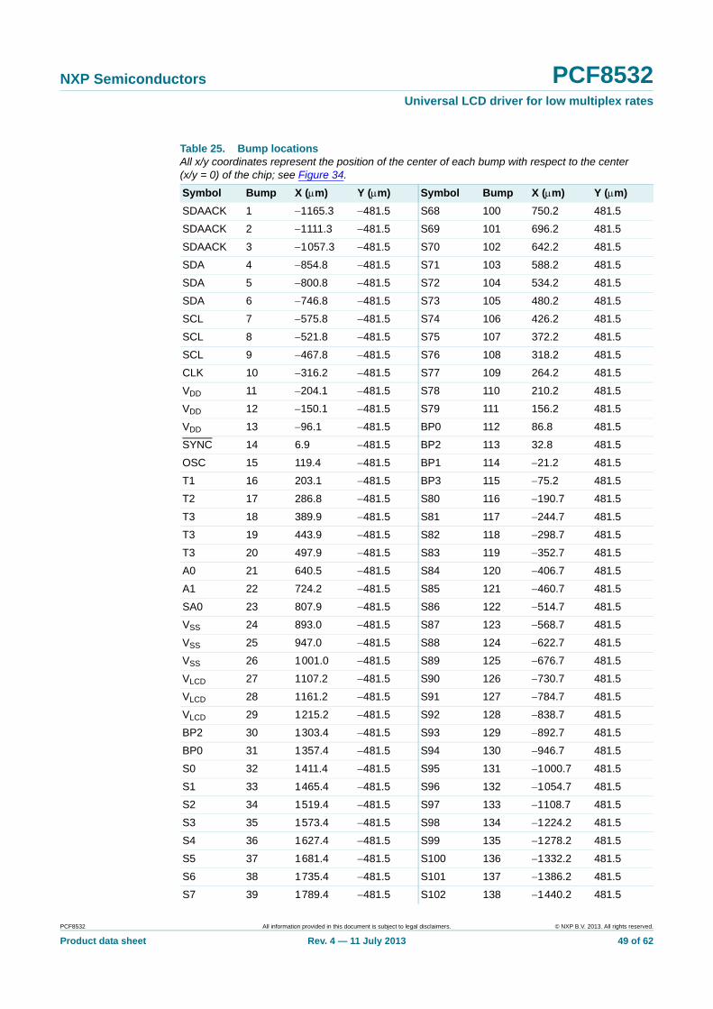
NXP Semiconductors PCF8532Universal LCD driver for low multiplex rates
Table 25. Bump locationsAll x/y coordinates represent the position of the center of each bump with respect to the center (x/y = 0) of the chip; see Figure 34.
Symbol Bump X (m) Y (m) Symbol Bump X (m) Y (m)
SDAACK 1 1165.3 481.5 S68 100 750.2 481.5
SDAACK 2 1111.3 481.5 S69 101 696.2 481.5
SDAACK 3 1057.3 481.5 S70 102 642.2 481.5
SDA 4 854.8 481.5 S71 103 588.2 481.5
SDA 5 800.8 481.5 S72 104 534.2 481.5
SDA 6 746.8 481.5 S73 105 480.2 481.5
SCL 7 575.8 481.5 S74 106 426.2 481.5
SCL 8 521.8 481.5 S75 107 372.2 481.5
SCL 9 467.8 481.5 S76 108 318.2 481.5
CLK 10 316.2 481.5 S77 109 264.2 481.5
VDD 11 204.1 481.5 S78 110 210.2 481.5
VDD 12 150.1 481.5 S79 111 156.2 481.5
VDD 13 96.1 481.5 BP0 112 86.8 481.5
SYNC 14 6.9 481.5 BP2 113 32.8 481.5
OSC 15 119.4 481.5 BP1 114 21.2 481.5
T1 16 203.1 481.5 BP3 115 75.2 481.5
T2 17 286.8 481.5 S80 116 190.7 481.5
T3 18 389.9 481.5 S81 117 244.7 481.5
T3 19 443.9 481.5 S82 118 298.7 481.5
T3 20 497.9 481.5 S83 119 352.7 481.5
A0 21 640.5 481.5 S84 120 406.7 481.5
A1 22 724.2 481.5 S85 121 460.7 481.5
SA0 23 807.9 481.5 S86 122 514.7 481.5
VSS 24 893.0 481.5 S87 123 568.7 481.5
VSS 25 947.0 481.5 S88 124 622.7 481.5
VSS 26 1001.0 481.5 S89 125 676.7 481.5
VLCD 27 1107.2 481.5 S90 126 730.7 481.5
VLCD 28 1161.2 481.5 S91 127 784.7 481.5
VLCD 29 1215.2 481.5 S92 128 838.7 481.5
BP2 30 1303.4 481.5 S93 129 892.7 481.5
BP0 31 1357.4 481.5 S94 130 946.7 481.5
S0 32 1411.4 481.5 S95 131 1000.7 481.5
S1 33 1465.4 481.5 S96 132 1054.7 481.5
S2 34 1519.4 481.5 S97 133 1108.7 481.5
S3 35 1573.4 481.5 S98 134 1224.2 481.5
S4 36 1627.4 481.5 S99 135 1278.2 481.5
S5 37 1681.4 481.5 S100 136 1332.2 481.5
S6 38 1735.4 481.5 S101 137 1386.2 481.5
S7 39 1789.4 481.5 S102 138 1440.2 481.5
PCF8532 All information provided in this document is subject to legal disclaimers. © NXP B.V. 2013. All rights reserved.
Product data sheet Rev. 4 — 11 July 2013 49 of 62

NXP Semiconductors PCF8532Universal LCD driver for low multiplex rates
S8 40 1843.4 481.5 S103 139 1494.2 481.5
S9 41 1897.4 481.5 S104 140 1548.2 481.5
S10 42 1951.4 481.5 S105 141 1602.2 481.5
S11 43 2005.4 481.5 S106 142 1656.2 481.5
S12 44 2059.4 481.5 S107 143 1710.2 481.5
S13 45 2113.4 481.5 S108 144 1764.2 481.5
S14 46 2167.4 481.5 S109 145 1818.2 481.5
S15 47 2221.4 481.5 S110 146 1872.2 481.5
S16 48 2363.9 481.5 S111 147 1926.2 481.5
S17 49 2417.9 481.5 S112 148 1980.2 481.5
S18 50 2471.9 481.5 S113 149 2034.2 481.5
S19 51 2525.9 481.5 S114 150 2088.2 481.5
S20 52 2579.9 481.5 S115 151 2142.2 481.5
S21 53 2633.9 481.5 S116 152 2284.7 481.5
S22 54 2687.9 481.5 S117 153 2338.7 481.5
S23 55 2741.9 481.5 S118 154 2392.7 481.5
S24 56 2795.9 481.5 S119 155 2446.7 481.5
S25 57 2849.9 481.5 S120 156 2500.7 481.5
S26 58 2903.9 481.5 S121 157 2554.7 481.5
S27 59 2957.9 481.5 S122 158 2608.7 481.5
S28 60 3011.9 481.5 S123 159 2662.7 481.5
S29 61 3067.7 481.5 S124 160 2716.7 481.5
S30 62 3013.7 481.5 S125 161 2770.7 481.5
S31 63 2959.7 481.5 S126 162 2824.7 481.5
S32 64 2905.7 481.5 S127 163 2878.7 481.5
S33 65 2851.7 481.5 S128 164 2932.7 481.5
S34 66 2797.7 481.5 S129 165 2986.7 481.5
S35 67 2743.7 481.5 S130 166 3040.7 481.5
S36 68 2689.7 481.5 S131 167 3025.2 481.5
S37 69 2635.7 481.5 S132 168 2971.2 481.5
S38 70 2520.2 481.5 S133 169 2917.2 481.5
S39 71 2466.2 481.5 S134 170 2863.2 481.5
S40 72 2412.2 481.5 S135 171 2809.2 481.5
S41 73 2358.2 481.5 S136 172 2755.2 481.5
S42 74 2304.2 481.5 S137 173 2701.2 481.5
S43 75 2250.2 481.5 S138 174 2647.2 481.5
S44 76 2196.2 481.5 S139 175 2593.2 481.5
S45 77 2142.2 481.5 S140 176 2539.2 481.5
S46 78 2088.2 481.5 S141 177 2485.2 481.5
Table 25. Bump locations …continuedAll x/y coordinates represent the position of the center of each bump with respect to the center (x/y = 0) of the chip; see Figure 34.
Symbol Bump X (m) Y (m) Symbol Bump X (m) Y (m)
PCF8532 All information provided in this document is subject to legal disclaimers. © NXP B.V. 2013. All rights reserved.
Product data sheet Rev. 4 — 11 July 2013 50 of 62

NXP Semiconductors PCF8532Universal LCD driver for low multiplex rates
The dummy bumps are connected to the pins shown in Table 26, but are not tested.
S47 79 2034.2 481.5 S142 178 2431.2 481.5
S48 80 1891.7 481.5 S143 179 2377.2 481.5
S49 81 1837.7 481.5 S144 180 2234.7 481.5
S50 82 1783.7 481.5 S145 181 2180.7 481.5
S51 83 1729.7 481.5 S146 182 2126.7 481.5
S52 84 1675.7 481.5 S147 183 2072.7 481.5
S53 85 1621.7 481.5 S148 184 2018.7 481.5
S54 86 1567.7 481.5 S149 185 1964.7 481.5
S55 87 1513.7 481.5 S150 186 1910.7 481.5
S56 88 1459.7 481.5 S151 187 1856.7 481.5
S57 89 1405.7 481.5 S152 188 1802.7 481.5
S58 90 1351.7 481.5 S153 189 1748.7 481.5
S59 91 1297.7 481.5 S154 190 1694.7 481.5
S60 92 1243.7 481.5 S155 191 1640.7 481.5
S61 93 1189.7 481.5 S156 192 1586.7 481.5
S62 94 1135.7 481.5 S157 193 1532.7 481.5
S63 95 1081.7 481.5 S158 194 1478.7 481.5
S64 96 1027.7 481.5 S159 195 1424.7 481.5
S65 97 973.7 481.5 BP3 196 1370.7 481.5
S66 98 858.2 481.5 BP1 197 1316.7 481.5
S67 99 804.2 481.5 - - - -
Table 26. Dummy bumpsAll x/y coordinates represent the position of the center of each bump with respect to the center (x/y = 0) of the chip; see Figure 34 on page 48.
Symbol Connected to pin X (m) Y (m)
D1 S131 3079.2 481.5
D2 S28 3065.9 481.5
D3 S29 3121.7 481.5
D4 S130 3094.7 481.5
Table 25. Bump locations …continuedAll x/y coordinates represent the position of the center of each bump with respect to the center (x/y = 0) of the chip; see Figure 34.
Symbol Bump X (m) Y (m) Symbol Bump X (m) Y (m)
PCF8532 All information provided in this document is subject to legal disclaimers. © NXP B.V. 2013. All rights reserved.
Product data sheet Rev. 4 — 11 July 2013 51 of 62

NXP Semiconductors PCF8532Universal LCD driver for low multiplex rates
The alignment marks are shown in Table 27.
Fig 35. Alignment marks
Table 27. Alignment marksAll x/y coordinates represent the position of the REF point (see Figure 35) with respect to the center (x/y = 0) of the chip; see Figure 34 on page 48.
a a1 a2 a3 b b1 b2 b3 Coordinates Unit
X Y
Alignment mark S1
121.5 - - - 121.5 - - - 2733.75 47.25 m
Alignment mark C1
121.5 36.45 48.6 36.45 121.5 36.45 48.6 36.45 2603.7 47.25 m
013aaa680
REF REF C1S1
a
b b
b1
b2
b3
aa1 a2 a3
PCF8532 All information provided in this document is subject to legal disclaimers. © NXP B.V. 2013. All rights reserved.
Product data sheet Rev. 4 — 11 July 2013 52 of 62

NXP Semiconductors PCF8532Universal LCD driver for low multiplex rates
16. Packing information
16.1 Tray information
Fig 36. Tray details
Table 28. Description of tray detailsTray details are shown in Figure 36.
Tray details
Dimensions
A B C D E F G H J K L M N O Unit
8.50 2.40 6.596 1.259 50.8 45.72 34.0 5.0 8.40 40.80 3.96 2.18 2.49 0.5 mm
Number of pockets
x direction y direction
5 18
PCF8532 All information provided in this document is subject to legal disclaimers. © NXP B.V. 2013. All rights reserved.
Product data sheet Rev. 4 — 11 July 2013 53 of 62

NXP Semiconductors PCF8532Universal LCD driver for low multiplex rates
Fig 37. Tray alignment
001aaj643
marking code
PCF8532 All information provided in this document is subject to legal disclaimers. © NXP B.V. 2013. All rights reserved.
Product data sheet Rev. 4 — 11 July 2013 54 of 62
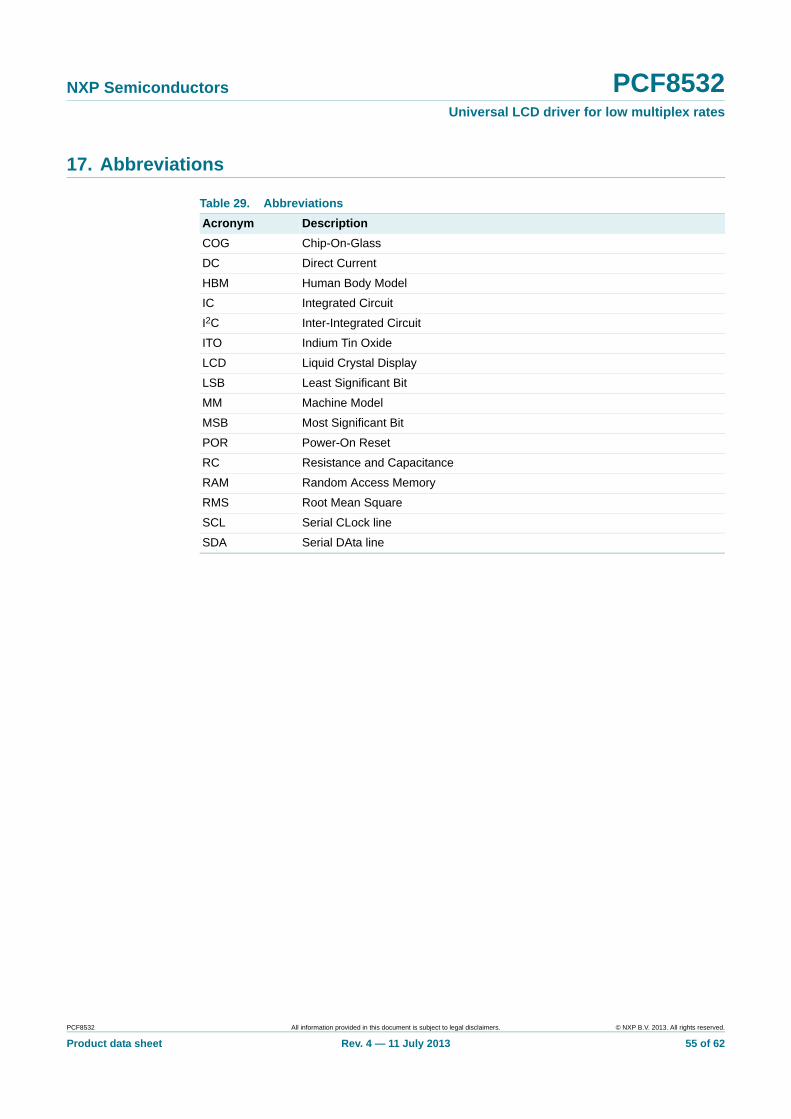
NXP Semiconductors PCF8532Universal LCD driver for low multiplex rates
17. Abbreviations
Table 29. Abbreviations
Acronym Description
COG Chip-On-Glass
DC Direct Current
HBM Human Body Model
IC Integrated Circuit
I2C Inter-Integrated Circuit
ITO Indium Tin Oxide
LCD Liquid Crystal Display
LSB Least Significant Bit
MM Machine Model
MSB Most Significant Bit
POR Power-On Reset
RC Resistance and Capacitance
RAM Random Access Memory
RMS Root Mean Square
SCL Serial CLock line
SDA Serial DAta line
PCF8532 All information provided in this document is subject to legal disclaimers. © NXP B.V. 2013. All rights reserved.
Product data sheet Rev. 4 — 11 July 2013 55 of 62

NXP Semiconductors PCF8532Universal LCD driver for low multiplex rates
18. References
[1] AN10170 — Design guidelines for COG modules with NXP monochrome LCD drivers
[2] AN10706 — Handling bare die
[3] AN11267 — EMC and system level ESD design guidelines for LCD drivers
[4] IEC 60134 — Rating systems for electronic tubes and valves and analogous semiconductor devices
[5] IEC 61340-5 — Protection of electronic devices from electrostatic phenomena
[6] JESD22-A114 — Electrostatic Discharge (ESD) Sensitivity Testing Human Body Model (HBM)
[7] JESD22-A115 — Electrostatic Discharge (ESD) Sensitivity Testing Machine Model (MM)
[8] JESD78 — IC Latch-Up Test
[9] JESD625-A — Requirements for Handling Electrostatic-Discharge-Sensitive (ESDS) Devices
[10] UM10204 — I2C-bus specification and user manual
[11] UM10569 — Store and transport requirements
PCF8532 All information provided in this document is subject to legal disclaimers. © NXP B.V. 2013. All rights reserved.
Product data sheet Rev. 4 — 11 July 2013 56 of 62

NXP Semiconductors PCF8532Universal LCD driver for low multiplex rates
19. Revision history
Table 30. Revision history
Document ID Release date Data sheet status Change notice Supersedes
PCF8532 v.4 20130711 Product data sheet - PCF8532 v.3
Modifications: • Changed tray information (Section 16.1)
PCF8532 v.3 20120905 Product data sheet - PCF8532 v.2
PCF8532 v.2 20110210 Product data sheet - PCF8532 v.1
PCF8532 v.1 20090210 Product data sheet - -
PCF8532 All information provided in this document is subject to legal disclaimers. © NXP B.V. 2013. All rights reserved.
Product data sheet Rev. 4 — 11 July 2013 57 of 62

NXP Semiconductors PCF8532Universal LCD driver for low multiplex rates
20. Legal information
20.1 Data sheet status
[1] Please consult the most recently issued document before initiating or completing a design.
[2] The term ‘short data sheet’ is explained in section “Definitions”.
[3] The product status of device(s) described in this document may have changed since this document was published and may differ in case of multiple devices. The latest product status information is available on the Internet at URL http://www.nxp.com.
20.2 Definitions
Draft — The document is a draft version only. The content is still under internal review and subject to formal approval, which may result in modifications or additions. NXP Semiconductors does not give any representations or warranties as to the accuracy or completeness of information included herein and shall have no liability for the consequences of use of such information.
Short data sheet — A short data sheet is an extract from a full data sheet with the same product type number(s) and title. A short data sheet is intended for quick reference only and should not be relied upon to contain detailed and full information. For detailed and full information see the relevant full data sheet, which is available on request via the local NXP Semiconductors sales office. In case of any inconsistency or conflict with the short data sheet, the full data sheet shall prevail.
Product specification — The information and data provided in a Product data sheet shall define the specification of the product as agreed between NXP Semiconductors and its customer, unless NXP Semiconductors and customer have explicitly agreed otherwise in writing. In no event however, shall an agreement be valid in which the NXP Semiconductors product is deemed to offer functions and qualities beyond those described in the Product data sheet.
20.3 Disclaimers
Limited warranty and liability — Information in this document is believed to be accurate and reliable. However, NXP Semiconductors does not give any representations or warranties, expressed or implied, as to the accuracy or completeness of such information and shall have no liability for the consequences of use of such information. NXP Semiconductors takes no responsibility for the content in this document if provided by an information source outside of NXP Semiconductors.
In no event shall NXP Semiconductors be liable for any indirect, incidental, punitive, special or consequential damages (including - without limitation - lost profits, lost savings, business interruption, costs related to the removal or replacement of any products or rework charges) whether or not such damages are based on tort (including negligence), warranty, breach of contract or any other legal theory.
Notwithstanding any damages that customer might incur for any reason whatsoever, NXP Semiconductors’ aggregate and cumulative liability towards customer for the products described herein shall be limited in accordance with the Terms and conditions of commercial sale of NXP Semiconductors.
Right to make changes — NXP Semiconductors reserves the right to make changes to information published in this document, including without limitation specifications and product descriptions, at any time and without notice. This document supersedes and replaces all information supplied prior to the publication hereof.
Suitability for use — NXP Semiconductors products are not designed, authorized or warranted to be suitable for use in life support, life-critical or safety-critical systems or equipment, nor in applications where failure or malfunction of an NXP Semiconductors product can reasonably be expected to result in personal injury, death or severe property or environmental damage. NXP Semiconductors and its suppliers accept no liability for inclusion and/or use of NXP Semiconductors products in such equipment or applications and therefore such inclusion and/or use is at the customer’s own risk.
Applications — Applications that are described herein for any of these products are for illustrative purposes only. NXP Semiconductors makes no representation or warranty that such applications will be suitable for the specified use without further testing or modification.
Customers are responsible for the design and operation of their applications and products using NXP Semiconductors products, and NXP Semiconductors accepts no liability for any assistance with applications or customer product design. It is customer’s sole responsibility to determine whether the NXP Semiconductors product is suitable and fit for the customer’s applications and products planned, as well as for the planned application and use of customer’s third party customer(s). Customers should provide appropriate design and operating safeguards to minimize the risks associated with their applications and products.
NXP Semiconductors does not accept any liability related to any default, damage, costs or problem which is based on any weakness or default in the customer’s applications or products, or the application or use by customer’s third party customer(s). Customer is responsible for doing all necessary testing for the customer’s applications and products using NXP Semiconductors products in order to avoid a default of the applications and the products or of the application or use by customer’s third party customer(s). NXP does not accept any liability in this respect.
Limiting values — Stress above one or more limiting values (as defined in the Absolute Maximum Ratings System of IEC 60134) will cause permanent damage to the device. Limiting values are stress ratings only and (proper) operation of the device at these or any other conditions above those given in the Recommended operating conditions section (if present) or the Characteristics sections of this document is not warranted. Constant or repeated exposure to limiting values will permanently and irreversibly affect the quality and reliability of the device.
Terms and conditions of commercial sale — NXP Semiconductors products are sold subject to the general terms and conditions of commercial sale, as published at http://www.nxp.com/profile/terms, unless otherwise agreed in a valid written individual agreement. In case an individual agreement is concluded only the terms and conditions of the respective agreement shall apply. NXP Semiconductors hereby expressly objects to applying the customer’s general terms and conditions with regard to the purchase of NXP Semiconductors products by customer.
No offer to sell or license — Nothing in this document may be interpreted or construed as an offer to sell products that is open for acceptance or the grant, conveyance or implication of any license under any copyrights, patents or other industrial or intellectual property rights.
Document status[1][2] Product status[3] Definition
Objective [short] data sheet Development This document contains data from the objective specification for product development.
Preliminary [short] data sheet Qualification This document contains data from the preliminary specification.
Product [short] data sheet Production This document contains the product specification.
PCF8532 All information provided in this document is subject to legal disclaimers. © NXP B.V. 2013. All rights reserved.
Product data sheet Rev. 4 — 11 July 2013 58 of 62
NXP Semiconductors PCF8532Universal LCD driver for low multiplex rates
Export control — This document as well as the item(s) described herein may be subject to export control regulations. Export might require a prior authorization from competent authorities.
Non-automotive qualified products — Unless this data sheet expressly states that this specific NXP Semiconductors product is automotive qualified, the product is not suitable for automotive use. It is neither qualified nor tested in accordance with automotive testing or application requirements. NXP Semiconductors accepts no liability for inclusion and/or use of non-automotive qualified products in automotive equipment or applications.
In the event that customer uses the product for design-in and use in automotive applications to automotive specifications and standards, customer (a) shall use the product without NXP Semiconductors’ warranty of the product for such automotive applications, use and specifications, and (b) whenever customer uses the product for automotive applications beyond NXP Semiconductors’ specifications such use shall be solely at customer’s own risk, and (c) customer fully indemnifies NXP Semiconductors for any liability, damages or failed product claims resulting from customer design and use of the product for automotive applications beyond NXP Semiconductors’ standard warranty and NXP Semiconductors’ product specifications.
Translations — A non-English (translated) version of a document is for reference only. The English version shall prevail in case of any discrepancy between the translated and English versions.
Bare die — All die are tested on compliance with their related technical specifications as stated in this data sheet up to the point of wafer sawing and are handled in accordance with the NXP Semiconductors storage and transportation conditions. If there are data sheet limits not guaranteed, these will be separately indicated in the data sheet. There are no post-packing tests performed on individual die or wafers.
NXP Semiconductors has no control of third party procedures in the sawing, handling, packing or assembly of the die. Accordingly, NXP Semiconductors assumes no liability for device functionality or performance of the die or systems after third party sawing, handling, packing or assembly of the die. It is the responsibility of the customer to test and qualify their application in which the die is used.
All die sales are conditioned upon and subject to the customer entering into a written die sale agreement with NXP Semiconductors through its legal department.
20.4 TrademarksNotice: All referenced brands, product names, service names and trademarks are the property of their respective owners.
I2C-bus — logo is a trademark of NXP B.V.
21. Contact information
For more information, please visit: http://www.nxp.com
For sales office addresses, please send an email to: [email protected]
PCF8532 All information provided in this document is subject to legal disclaimers. © NXP B.V. 2013. All rights reserved.
Product data sheet Rev. 4 — 11 July 2013 59 of 62
NXP Semiconductors PCF8532Universal LCD driver for low multiplex rates
22. Tables
Table 1. Ordering information. . . . . . . . . . . . . . . . . . . . . .2Table 2. Ordering options . . . . . . . . . . . . . . . . . . . . . . . . .2Table 3. Marking codes . . . . . . . . . . . . . . . . . . . . . . . . . .2Table 4. Pin description . . . . . . . . . . . . . . . . . . . . . . . . . .5Table 5. Definition of PCF8532 commands . . . . . . . . . . .6Table 6. Mode-set - command bit description . . . . . . . . .6Table 7. Load-data-pointer-MSB - command bit
description . . . . . . . . . . . . . . . . . . . . . . . . . . . . .7Table 8. Load-data-pointer-LSB - command bit
description . . . . . . . . . . . . . . . . . . . . . . . . . . . . .7Table 9. Device-select - command bit description . . . . . .7Table 10. Bank-select - command bit description . . . . . . .8Table 11. Blink-select - command bit description . . . . . . .8Table 12. Frequency-ctrl - command bit description . . . .10Table 13. Blink frequencies . . . . . . . . . . . . . . . . . . . . . . . 11Table 14. Selection of possible display configurations . . .12Table 15. Biasing characteristics . . . . . . . . . . . . . . . . . . .13Table 16. Standard RAM filling in 1:3 multiplex drive
mode. . . . . . . . . . . . . . . . . . . . . . . . . . . . . . . . .25Table 17. Entire RAM filling by rewriting in 1:3 multiplex
drive mode . . . . . . . . . . . . . . . . . . . . . . . . . . . .25Table 18. I2C slave address byte . . . . . . . . . . . . . . . . . . .30Table 19. Control byte description . . . . . . . . . . . . . . . . . .31Table 20. Limiting values . . . . . . . . . . . . . . . . . . . . . . . . .35Table 21. Static characteristics . . . . . . . . . . . . . . . . . . . .36Table 22. Dynamic characteristics . . . . . . . . . . . . . . . . . .38Table 23. Addressing cascaded PCF8532 . . . . . . . . . . .43Table 24. SYNC contact resistance . . . . . . . . . . . . . . . . .44Table 25. Bump locations . . . . . . . . . . . . . . . . . . . . . . . .49Table 26. Dummy bumps . . . . . . . . . . . . . . . . . . . . . . . . .51Table 27. Alignment marks. . . . . . . . . . . . . . . . . . . . . . . .52Table 28. Description of tray details . . . . . . . . . . . . . . . . .53Table 29. Abbreviations . . . . . . . . . . . . . . . . . . . . . . . . . .55Table 30. Revision history . . . . . . . . . . . . . . . . . . . . . . . .57
PCF8532 All information provided in this document is subject to legal disclaimers. © NXP B.V. 2013. All rights reserved.
Product data sheet Rev. 4 — 11 July 2013 60 of 62
NXP Semiconductors PCF8532Universal LCD driver for low multiplex rates
23. Figures
Fig 1. Block diagram of PCF8532 . . . . . . . . . . . . . . . . . .3Fig 2. Pinning diagram of PCF8532. . . . . . . . . . . . . . . . .4Fig 3. Frequency generation of the PCF8532 . . . . . . . . .9Fig 4. Example of displays suitable for PCF8532 . . . . .12Fig 5. Typical system configuration . . . . . . . . . . . . . . . .12Fig 6. Electro-optical characteristic: relative
transmission curve of the liquid . . . . . . . . . . . . . .15Fig 7. Static drive mode waveforms. . . . . . . . . . . . . . . .16Fig 8. Waveforms for the 1:2 multiplex drive mode
with 1⁄2 bias . . . . . . . . . . . . . . . . . . . . . . . . . . . . .17Fig 9. Waveforms for the 1:2 multiplex drive mode
with 1⁄3 bias . . . . . . . . . . . . . . . . . . . . . . . . . . . . .18Fig 10. Waveforms for the 1:3 multiplex drive mode
with 1⁄3 bias . . . . . . . . . . . . . . . . . . . . . . . . . . . . .19Fig 11. Waveforms for the 1:4 multiplex drive mode
with 1⁄3 bias . . . . . . . . . . . . . . . . . . . . . . . . . . . . .20Fig 12. Display RAM bitmap . . . . . . . . . . . . . . . . . . . . . .22Fig 13. Relationships between LCD layout, drive mode,
display RAM filling order, and display data transmitted over the I2C-bus . . . . . . . . . . . . . . . .23
Fig 14. RAM banks in static and multiplex driving mode 1:2 . . . . . . . . . . . . . . . . . . . . . . . . . . . . . . .26
Fig 15. Bank selection . . . . . . . . . . . . . . . . . . . . . . . . . . .27Fig 16. Example of the Bank-select command with
multiplex drive mode 1:2 . . . . . . . . . . . . . . . . . . .27Fig 17. Bit transfer . . . . . . . . . . . . . . . . . . . . . . . . . . . . . .28Fig 18. Definition of START and STOP conditions. . . . . .29Fig 19. System configuration . . . . . . . . . . . . . . . . . . . . . .29Fig 20. Acknowledgement on the I2C-bus . . . . . . . . . . . .30Fig 21. I2C-bus protocol . . . . . . . . . . . . . . . . . . . . . . . . . .31Fig 22. Control byte format . . . . . . . . . . . . . . . . . . . . . . .32Fig 23. Device protection diagram . . . . . . . . . . . . . . . . . .33Fig 24. IDD(LCD) (typical) with respect to VLCD . . . . . . . . .37Fig 25. Driver timing waveforms . . . . . . . . . . . . . . . . . . .39Fig 26. I2C-bus timing waveforms . . . . . . . . . . . . . . . . . .39Fig 27. Values for RPU(max). . . . . . . . . . . . . . . . . . . . . . . .41Fig 28. Values for RPU(min) . . . . . . . . . . . . . . . . . . . . . . . .41Fig 29. Operating range of the PCF8532 with respect
to the ITO track resistance. . . . . . . . . . . . . . . . . .42Fig 30. SDA, SDAACK configurations . . . . . . . . . . . . . . .43Fig 31. Cascaded configuration with two PCF8532
using the internal clock of the master . . . . . . . . .45Fig 32. Cascaded configuration with one PCF8532
and one PCF8533 using the internal clock of the master . . . . . . . . . . . . . . . . . . . . . . . . . . . . . .46
Fig 33. Synchronization of the cascade for the various PCF8532 drive modes . . . . . . . . . . . . . . . . . . . . .47
Fig 34. Bare die outline of PCF8532U . . . . . . . . . . . . . . .48Fig 35. Alignment marks . . . . . . . . . . . . . . . . . . . . . . . . .52Fig 36. Tray details . . . . . . . . . . . . . . . . . . . . . . . . . . . . .53Fig 37. Tray alignment . . . . . . . . . . . . . . . . . . . . . . . . . . .54
PCF8532 All information provided in this document is subject to legal disclaimers. © NXP B.V. 2013. All rights reserved.
Product data sheet Rev. 4 — 11 July 2013 61 of 62

NXP Semiconductors PCF8532Universal LCD driver for low multiplex rates
24. Contents
1 General description . . . . . . . . . . . . . . . . . . . . . . 1
2 Features and benefits . . . . . . . . . . . . . . . . . . . . 1
3 Ordering information. . . . . . . . . . . . . . . . . . . . . 23.1 Ordering options . . . . . . . . . . . . . . . . . . . . . . . . 2
4 Marking . . . . . . . . . . . . . . . . . . . . . . . . . . . . . . . . 2
5 Block diagram . . . . . . . . . . . . . . . . . . . . . . . . . . 3
6 Pinning information. . . . . . . . . . . . . . . . . . . . . . 46.1 Pinning . . . . . . . . . . . . . . . . . . . . . . . . . . . . . . . 46.2 Pin description . . . . . . . . . . . . . . . . . . . . . . . . . 5
7 Functional description . . . . . . . . . . . . . . . . . . . 67.1 Commands of PCF8532 . . . . . . . . . . . . . . . . . . 67.1.1 Command: mode-set . . . . . . . . . . . . . . . . . . . . 67.1.2 Command: load-data-pointer . . . . . . . . . . . . . . 77.1.3 Command: device-select . . . . . . . . . . . . . . . . . 77.1.4 Command: bank-select. . . . . . . . . . . . . . . . . . . 87.1.5 Command: blink-select . . . . . . . . . . . . . . . . . . . 87.1.6 Clock frequency and timing . . . . . . . . . . . . . . . 87.1.6.1 Clock source selection . . . . . . . . . . . . . . . . . . . 97.1.6.2 Internal clock . . . . . . . . . . . . . . . . . . . . . . . . . . 97.1.6.3 External clock . . . . . . . . . . . . . . . . . . . . . . . . . . 97.1.6.4 Frame frequency . . . . . . . . . . . . . . . . . . . . . . 107.1.6.5 Command: frequency-ctrl . . . . . . . . . . . . . . . . 107.1.6.6 Blinking . . . . . . . . . . . . . . . . . . . . . . . . . . . . . . 107.2 Power-On Reset (POR) . . . . . . . . . . . . . . . . . 117.3 Possible display configurations . . . . . . . . . . . 117.3.1 LCD bias generator . . . . . . . . . . . . . . . . . . . . 137.3.2 Display register . . . . . . . . . . . . . . . . . . . . . . . . 137.3.3 LCD voltage selector . . . . . . . . . . . . . . . . . . . 137.3.3.1 Electro-optical performance . . . . . . . . . . . . . . 147.3.4 LCD drive mode waveforms . . . . . . . . . . . . . . 167.3.4.1 Static drive mode . . . . . . . . . . . . . . . . . . . . . . 167.3.4.2 1:2 multiplex drive mode. . . . . . . . . . . . . . . . . 177.3.4.3 1:3 multiplex drive mode. . . . . . . . . . . . . . . . . 197.3.4.4 1:4 multiplex drive mode. . . . . . . . . . . . . . . . . 207.4 Backplane and segment outputs . . . . . . . . . . 217.4.1 Backplane outputs . . . . . . . . . . . . . . . . . . . . . 217.4.2 Segment outputs. . . . . . . . . . . . . . . . . . . . . . . 217.5 Display RAM. . . . . . . . . . . . . . . . . . . . . . . . . . 217.5.1 Data pointer . . . . . . . . . . . . . . . . . . . . . . . . . . 247.5.2 Subaddress counter . . . . . . . . . . . . . . . . . . . . 247.5.3 RAM writing in 1:3 multiplex drive mode. . . . . 257.5.4 Bank selection . . . . . . . . . . . . . . . . . . . . . . . . 257.5.4.1 Output bank selector . . . . . . . . . . . . . . . . . . . 257.5.4.2 Input bank selector . . . . . . . . . . . . . . . . . . . . . 267.5.4.3 RAM bank switching . . . . . . . . . . . . . . . . . . . . 26
8 Characteristics of the I2C-bus . . . . . . . . . . . . 28
8.1 Bit transfer . . . . . . . . . . . . . . . . . . . . . . . . . . . 288.1.1 START and STOP conditions. . . . . . . . . . . . . 288.2 System configuration . . . . . . . . . . . . . . . . . . . 298.3 Acknowledge . . . . . . . . . . . . . . . . . . . . . . . . . 298.4 I2C-bus controller . . . . . . . . . . . . . . . . . . . . . . 308.5 Input filters . . . . . . . . . . . . . . . . . . . . . . . . . . . 308.6 I2C-bus protocol . . . . . . . . . . . . . . . . . . . . . . . 30
9 Internal circuitry . . . . . . . . . . . . . . . . . . . . . . . 33
10 Safety notes. . . . . . . . . . . . . . . . . . . . . . . . . . . 34
11 Limiting values . . . . . . . . . . . . . . . . . . . . . . . . 35
12 Static characteristics . . . . . . . . . . . . . . . . . . . 36
13 Dynamic characteristics. . . . . . . . . . . . . . . . . 38
14 Application information . . . . . . . . . . . . . . . . . 4014.1 Pull-up resistor sizing on I2C-bus. . . . . . . . . . 4014.1.1 Max value of pull-up resistor . . . . . . . . . . . . . 4014.1.2 Min value of pull-up resistor . . . . . . . . . . . . . . 4014.2 ITO track resistance . . . . . . . . . . . . . . . . . . . . 4114.3 SDA and SDAACK configuration . . . . . . . . . . 4314.4 Cascaded operation. . . . . . . . . . . . . . . . . . . . 43
15 Bare die outline . . . . . . . . . . . . . . . . . . . . . . . . 48
16 Packing information . . . . . . . . . . . . . . . . . . . . 5316.1 Tray information . . . . . . . . . . . . . . . . . . . . . . . 53
17 Abbreviations . . . . . . . . . . . . . . . . . . . . . . . . . 55
18 References. . . . . . . . . . . . . . . . . . . . . . . . . . . . 56
19 Revision history . . . . . . . . . . . . . . . . . . . . . . . 57
20 Legal information . . . . . . . . . . . . . . . . . . . . . . 5820.1 Data sheet status . . . . . . . . . . . . . . . . . . . . . . 5820.2 Definitions . . . . . . . . . . . . . . . . . . . . . . . . . . . 5820.3 Disclaimers . . . . . . . . . . . . . . . . . . . . . . . . . . 5820.4 Trademarks . . . . . . . . . . . . . . . . . . . . . . . . . . 59
21 Contact information . . . . . . . . . . . . . . . . . . . . 59
22 Tables . . . . . . . . . . . . . . . . . . . . . . . . . . . . . . . . 60
23 Figures . . . . . . . . . . . . . . . . . . . . . . . . . . . . . . . 61
24 Contents. . . . . . . . . . . . . . . . . . . . . . . . . . . . . . 62
© NXP B.V. 2013. All rights reserved.
For more information, please visit: http://www.nxp.comFor sales office addresses, please send an email to: [email protected]
Date of release: 11 July 2013
Document identifier: PCF8532
Please be aware that important notices concerning this document and the product(s)described herein, have been included in section ‘Legal information’.