LCD driver for low multiplex rates - NXP Semiconductors · 1998 Jun 18 3 Philips Semiconductors...
28
DATA SHEET Product specification File under Integrated Circuits, IC12 1998 Jun 18 INTEGRATED CIRCUITS OM4068 LCD driver for low multiplex rates
Transcript of LCD driver for low multiplex rates - NXP Semiconductors · 1998 Jun 18 3 Philips Semiconductors...
DATA SHEET
Product specificationFile under Integrated Circuits, IC12
1998 Jun 18
INTEGRATED CIRCUITS
OM4068LCD driver for low multiplex rates
1998 Jun 18 2
Philips Semiconductors Product specification
LCD driver for low multiplex rates OM4068
FEATURES
• Single-chip LCD controller/driver
• Static/duplex/triplex drive modes with up to32/64/96 LCD segments drive capability per device
• Selectable backplane drive configuration: static or2 or 3 backplane multiplexing
• Selectable display bias configuration drive: static, 1⁄2 or1⁄3
• 32 segment drivers
• Serial data input (word length 32 to 96 bits)
• On-chip generation of intermediate LCD bias voltages
• 2 MHz fast serial bus interface
• CMOS compatible
• Compatible with any 4-bit, 8-bit or 16-bitmicroprocessors/microcontrollers
• May be cascaded for large LCD applications
• Logic supply voltage range (VDD − VSS) of 2.5 to 5.5 V
• Display supply voltage range (VLCD − VSS) of3.5 to 6.5 V
• Low power consumption, suitable for battery operatedsystems
• No external components needed by the oscillator
• Manufactured in silicon gate CMOS process.
APPLICATIONS
• Telecom equipment
• Portable instruments
• Alarm systems
• Automotive equipment.
GENERAL DESCRIPTION
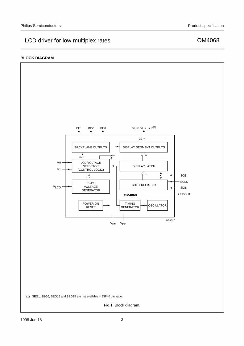
The OM4068 is a low-power CMOS LCD driver, designedto drive Liquid Crystal Displays (LCDs) with low multiplexrates. It generates the drive signals for any static ormultiplexed LCD containing up to three backplanes and upto 32 segment lines and can be easily cascaded for largerLCD applications. All necessary functions for the displayare provided in a single chip, including on-chip generationof LCD bias voltages, resulting in a minimum of externalcomponents and lower power consumption. A 3-line busstructure enables serial data transfer with mostmicroprocessors/microcontrollers. All inputs are CMOScompatible.
ORDERING INFORMATION
Notes
1. Gull Wing package.
2. For details see Chapter “Bonding pad locations”.
TYPE NUMBERPACKAGE
NAME DESCRIPTION VERSION
OM4068H(1) QFP44 plastic quad flat package; 44 leads (lead length 1.3 mm);body 10 × 10 × 1.75 mm
SOT307-2
OM4068P DIP40 plastic dual in-line package; 40 leads (600 mil) SOT129-1
OM4068U/5(2) die unsawn wafer −OM4068U tray chip in tray −
1998 Jun 18 3
Philips Semiconductors Product specification
LCD driver for low multiplex rates OM4068
BLOCK DIAGRAM
Fig.1 Block diagram.
handbook, full pagewidth
MBK817
BACKPLANE OUTPUTS
OM4068
LCD VOLTAGESELECTOR
(CONTROL LOGIC)
BP2BP1 BP3 SEG1 to SEG32(1)
DISPLAY SEGMENT OUTPUTS
TIMINGGENERATOR
VSS VDD
DISPLAY LATCH
OSCILLATOR
BIASVOLTAGE
GENERATOR
POWER-ONRESET
44
M0
M1
VLCD
32
4
SHIFT REGISTER
SCE
SCLK
SDIN
SDOUT
(1) SEG1, SEG6, SEG15 and SEG25 are not available in DIP40 package.
1998 Jun 18 4
Philips Semiconductors Product specification
LCD driver for low multiplex rates OM4068
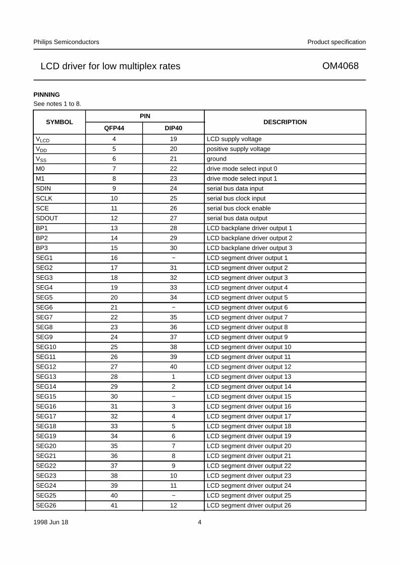
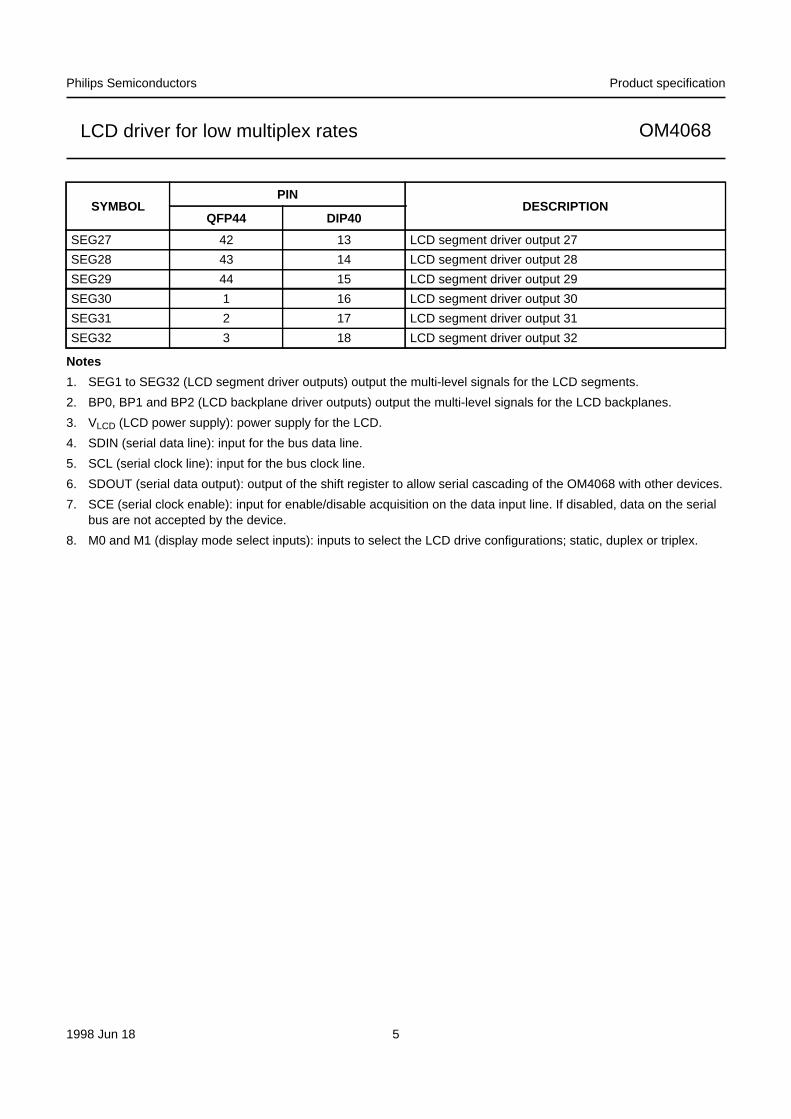
PINNINGSee notes 1 to 8.
SYMBOLPIN
DESCRIPTIONQFP44 DIP40
VLCD 4 19 LCD supply voltage
VDD 5 20 positive supply voltage
VSS 6 21 ground
M0 7 22 drive mode select input 0
M1 8 23 drive mode select input 1
SDIN 9 24 serial bus data input
SCLK 10 25 serial bus clock input
SCE 11 26 serial bus clock enable
SDOUT 12 27 serial bus data output
BP1 13 28 LCD backplane driver output 1
BP2 14 29 LCD backplane driver output 2
BP3 15 30 LCD backplane driver output 3
SEG1 16 − LCD segment driver output 1
SEG2 17 31 LCD segment driver output 2
SEG3 18 32 LCD segment driver output 3
SEG4 19 33 LCD segment driver output 4
SEG5 20 34 LCD segment driver output 5
SEG6 21 − LCD segment driver output 6
SEG7 22 35 LCD segment driver output 7
SEG8 23 36 LCD segment driver output 8
SEG9 24 37 LCD segment driver output 9
SEG10 25 38 LCD segment driver output 10
SEG11 26 39 LCD segment driver output 11
SEG12 27 40 LCD segment driver output 12
SEG13 28 1 LCD segment driver output 13
SEG14 29 2 LCD segment driver output 14
SEG15 30 − LCD segment driver output 15
SEG16 31 3 LCD segment driver output 16
SEG17 32 4 LCD segment driver output 17
SEG18 33 5 LCD segment driver output 18
SEG19 34 6 LCD segment driver output 19
SEG20 35 7 LCD segment driver output 20
SEG21 36 8 LCD segment driver output 21
SEG22 37 9 LCD segment driver output 22
SEG23 38 10 LCD segment driver output 23
SEG24 39 11 LCD segment driver output 24
SEG25 40 − LCD segment driver output 25
SEG26 41 12 LCD segment driver output 26
1998 Jun 18 5
Philips Semiconductors Product specification
LCD driver for low multiplex rates OM4068
Notes
1. SEG1 to SEG32 (LCD segment driver outputs) output the multi-level signals for the LCD segments.
2. BP0, BP1 and BP2 (LCD backplane driver outputs) output the multi-level signals for the LCD backplanes.
3. VLCD (LCD power supply): power supply for the LCD.
4. SDIN (serial data line): input for the bus data line.
5. SCL (serial clock line): input for the bus clock line.
6. SDOUT (serial data output): output of the shift register to allow serial cascading of the OM4068 with other devices.
7. SCE (serial clock enable): input for enable/disable acquisition on the data input line. If disabled, data on the serialbus are not accepted by the device.
8. M0 and M1 (display mode select inputs): inputs to select the LCD drive configurations; static, duplex or triplex.
SEG27 42 13 LCD segment driver output 27
SEG28 43 14 LCD segment driver output 28
SEG29 44 15 LCD segment driver output 29
SEG30 1 16 LCD segment driver output 30
SEG31 2 17 LCD segment driver output 31
SEG32 3 18 LCD segment driver output 32
SYMBOLPIN
DESCRIPTIONQFP44 DIP40
1998 Jun 18 6
Philips Semiconductors Product specification
LCD driver for low multiplex rates OM4068
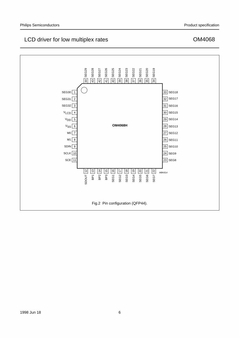
Fig.2 Pin configuration (QFP44).
handbook, full pagewidth
OM4068H
MBK814
1SEG30
SEG31
SEG32
M0
M1
SDIN
SCLK
SCE
SD
OU
T
BP
1
BP
2
BP
3
SE
G1
SE
G2
SE
G3
SE
G4
SE
G5
SE
G6
SE
G7
SEG8
SEG9
SEG10
SEG11
SEG12
SEG13
SEG14
SEG15
SEG16
SEG17
SEG18
SE
G19
SE
G20
SE
G21
SE
G22
SE
G23
SE
G24
SE
G25
SE
G26
SE
G27
SE
G28
SE
G29
VLCD
VDD
VSS
2
3
4
5
6
7
8
9
10
11
33
32
31
30
29
28
27
26
25
24
23
12 13 14 15 16 17 18 19 20 21 22
44 43 42 41 40 39 38 37 36 35 34
1998 Jun 18 7
Philips Semiconductors Product specification
LCD driver for low multiplex rates OM4068
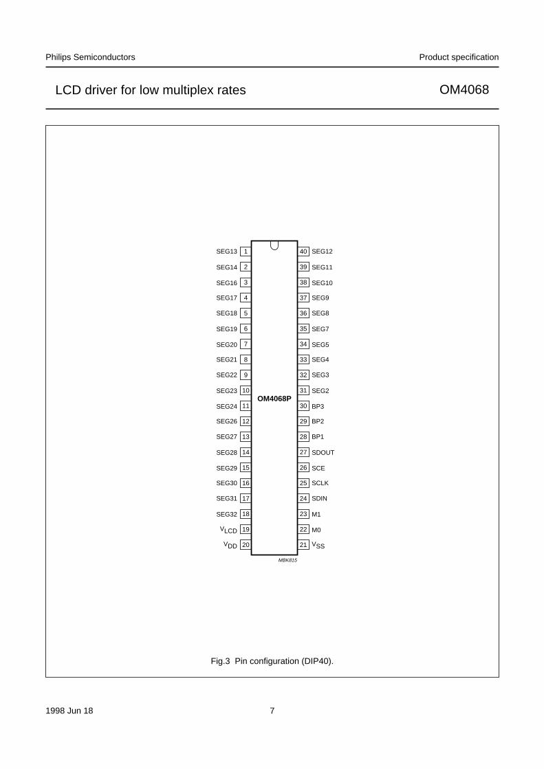
Fig.3 Pin configuration (DIP40).
handbook, halfpage
OM4068P
MBK815
1
2
3
4
5
6
7
8
9
10
11
12
13
14
15
16
17
18
19
20
40
39
38
37
36
35
34
33
32
31
30
29
28
27
26
25
24
23
22
21
SEG13 SEG12
SEG14 SEG11
SEG16 SEG10
SEG17 SEG9
SEG18 SEG8
SEG19 SEG7
SEG20 SEG5
SEG21 SEG4
SEG22 SEG3
SEG23 SEG2
SEG24 BP3
SEG26 BP2
SEG27 BP1
SEG28 SDOUT
SEG29 SCE
SEG30 SCLK
SEG31 SDIN
SEG32 M1
VLCD M0
VDD VSS
1998 Jun 18 8
Philips Semiconductors Product specification
LCD driver for low multiplex rates OM4068
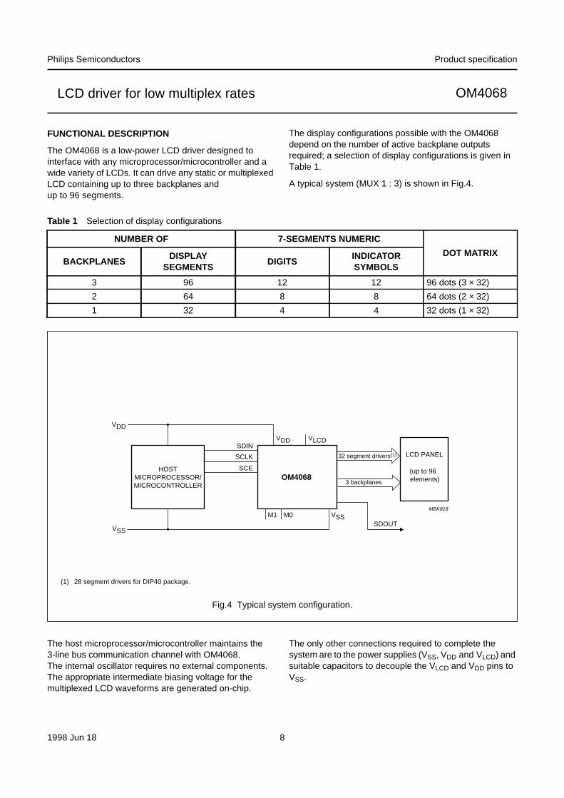
FUNCTIONAL DESCRIPTION
The OM4068 is a low-power LCD driver designed tointerface with any microprocessor/microcontroller and awide variety of LCDs. It can drive any static or multiplexedLCD containing up to three backplanes andup to 96 segments.
The display configurations possible with the OM4068depend on the number of active backplane outputsrequired; a selection of display configurations is given inTable 1.
A typical system (MUX 1 : 3) is shown in Fig.4.
Table 1 Selection of display configurations
NUMBER OF 7-SEGMENTS NUMERIC
DOT MATRIXBACKPLANES
DISPLAYSEGMENTS
DIGITSINDICATORSYMBOLS
3 96 12 12 96 dots (3 × 32)
2 64 8 8 64 dots (2 × 32)
1 32 4 4 32 dots (1 × 32)
Fig.4 Typical system configuration.
handbook, full pagewidth
HOSTMICROPROCESSOR/MICROCONTROLLER
SCLK
SDOUT
SCE
SDIN
32 segment drivers(1)
3 backplanes
LCD PANEL
(up to 96 elements)OM4068
M1 M0
VDD
VDD VLCD
VSS
VSSMBK818
(1) 28 segment drivers for DIP40 package.
The host microprocessor/microcontroller maintains the3-line bus communication channel with OM4068.The internal oscillator requires no external components.The appropriate intermediate biasing voltage for themultiplexed LCD waveforms are generated on-chip.
The only other connections required to complete thesystem are to the power supplies (VSS, VDD and VLCD) andsuitable capacitors to decouple the VLCD and VDD pins toVSS.
1998 Jun 18 9
Philips Semiconductors Product specification
LCD driver for low multiplex rates OM4068
Power-on reset
The on-chip power-on reset block initializes the chip afterpower-on or power failures. The OM4068 resets to astarting condition as follows:
• All backplane and segment outputs are set to VSS(display off)
• All shift registers and latches are set in 3-state
• SDOUT (allowing serial cascading) is set to logic 0 (withSCE LOW)
• Power-down mode.
Data transfers on the serial bus should be avoided for0.5 ms following power-on to allow completion of the resetaction.
Power-down
After power-on the chip is in power-down mode as long asthe serial clock is not active. During power-down all staticcurrents are switched off (no internal oscillator, no timingand no bias level generation) and all LCD-outputs are3-stated. The power-on reset functions remain enabled.
The power-down mode is disabled at the first rising edgeof the serial clock SCLK.
LCD bias voltage generator
The intermediate bias voltages for the LCD display aregenerated on-chip. This removes the need for an externalresistive bias chain and significantly reduces the systempower consumption. The full-scale LCD voltage VOPequals VLCD − VSS. The optimum value of VOP depends onthe LCD threshold voltage (Vth) and the number of biaslevels.
Fractional LCD biasing voltages are obtained from aninternal voltage divider of three series resistors (1⁄3bias)connected between VLCD and VSS. The centre resistor canbe switched out of the circuit to provide a 1⁄2bias voltagelevel for the 1 : 2 multiplex configuration.
The bias levels depend on the multiplex rate and areselected automatically when the display configuration isselected using M1 and M0.
LCD voltage selector
The LCD voltage selector (control logic) coordinates themultiplexing of the LCD in accordance with the selecteddrive or display configuration. The operation of the voltageselector is controlled by the input pins M0 and M1(see Table 2).
Table 2 Drive mode selection
For multiplex rates of 1 : 2 three bias levels are usedincluding VLCD and VSS. Four bias level are used for the1 : 3 multiplex rate. The various biasing configurationstogether with the biasing characteristics as functions ofVOP = VLCD − VSS and the resulting discrimination ratios(D), are given in Table 3.
A practical value for VOP is determinated by equatingVoff(rms) with a defined LCD threshold voltage (Vth),typically when the LCD exhibits approximately 10%contrast. In static mode a suitable choice is VOP > 3Vth.
M1 M0 DRIVE MODE
0 0 test mode (not user accessible)
0 1 static drive (1 : 1)
1 0 duplex drive (1 : 2)
1 1 triplex drive (1 : 3)
1998 Jun 18 10
Philips Semiconductors Product specification
LCD driver for low multiplex rates OM4068
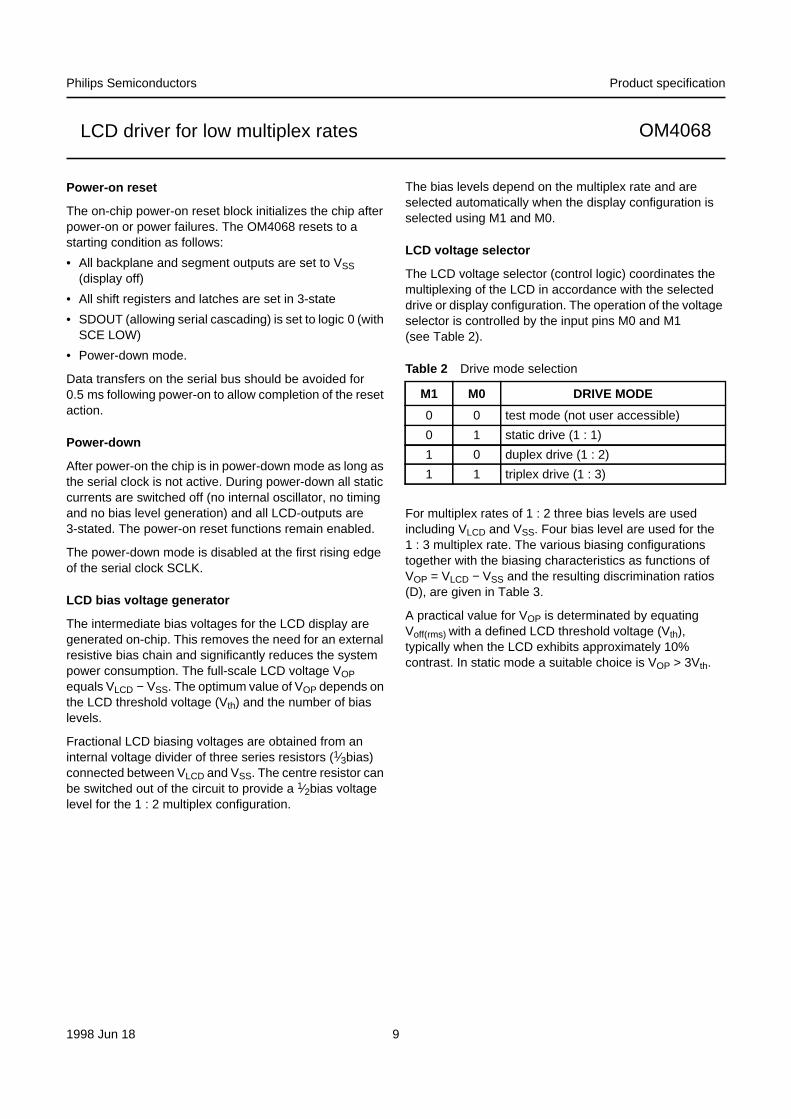
Table 3 LCD drive modes: summary of characteristics
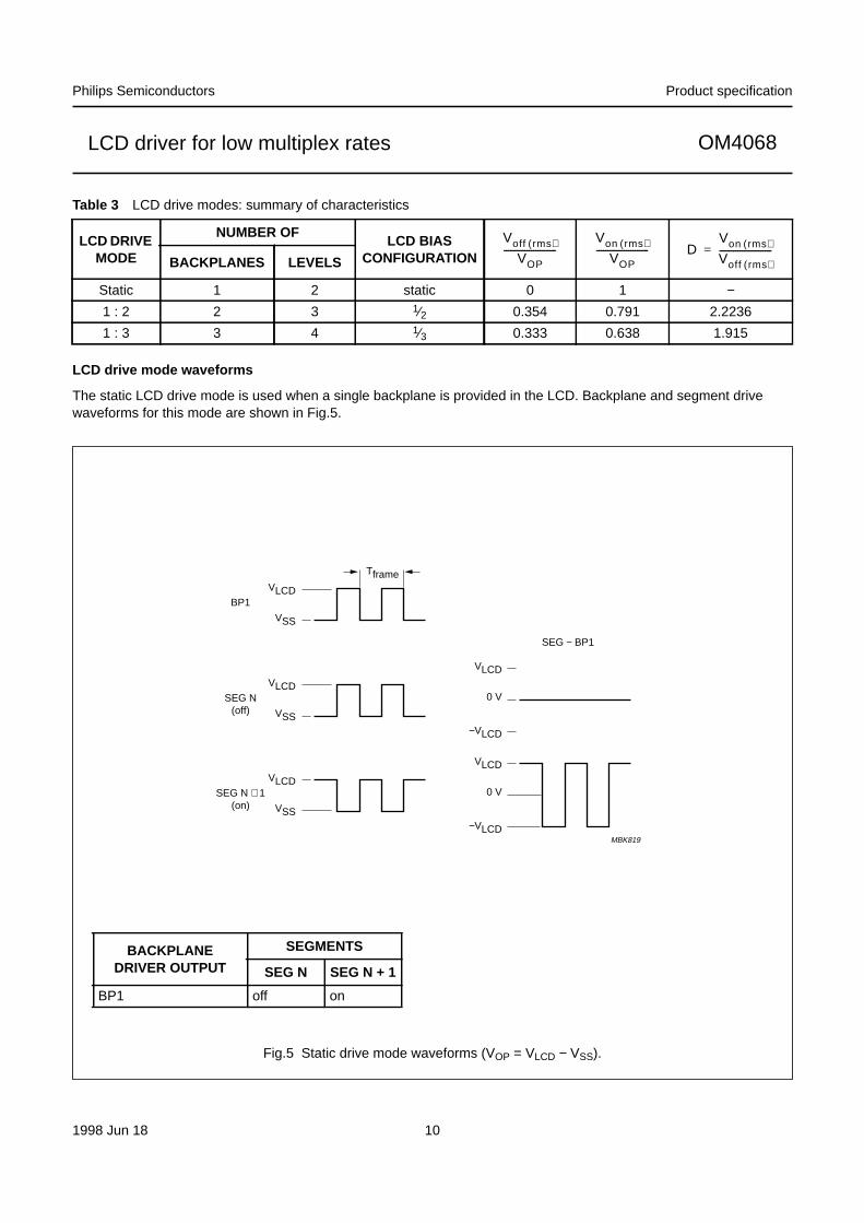
LCD drive mode waveforms
The static LCD drive mode is used when a single backplane is provided in the LCD. Backplane and segment drivewaveforms for this mode are shown in Fig.5.
LCD DRIVEMODE
NUMBER OFLCD BIAS
CONFIGURATIONBACKPLANES LEVELS
Static 1 2 static 0 1 −1 : 2 2 3 1⁄2 0.354 0.791 2.2236
1 : 3 3 4 1⁄3 0.333 0.638 1.915
Voff rms( )VOP
-----------------------Von rms( )
VOP----------------------- D
Von rms( )Voff rms( )-----------------------=
Fig.5 Static drive mode waveforms (VOP = VLCD − VSS).
BACKPLANEDRIVER OUTPUT
SEGMENTS
SEG N SEG N + 1
BP1 off on
handbook, full pagewidth
MBK819
VLCDBP1
VSS
Tframe
VLCDSEG N
(off)
SEG − BP1
VSS
VLCD
VLCD
0 V
−VLCD
SEG N + 1(on) VSS
VLCD
0 V
−VLCD
1998 Jun 18 11
Philips Semiconductors Product specification
LCD driver for low multiplex rates OM4068
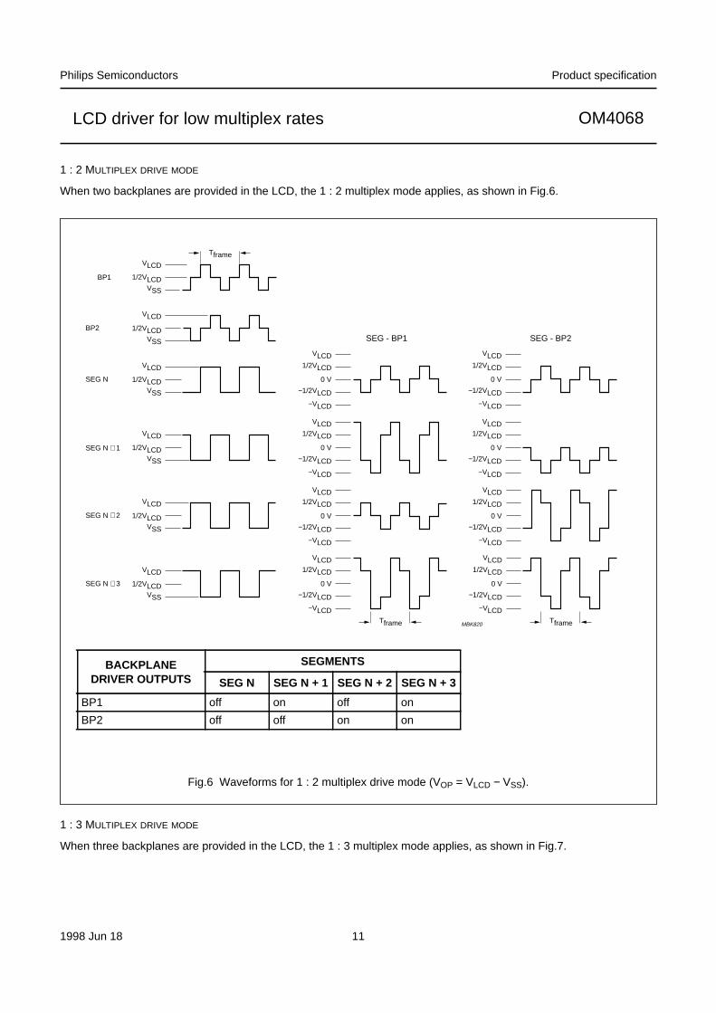
1 : 2 MULTIPLEX DRIVE MODE
When two backplanes are provided in the LCD, the 1 : 2 multiplex mode applies, as shown in Fig.6.
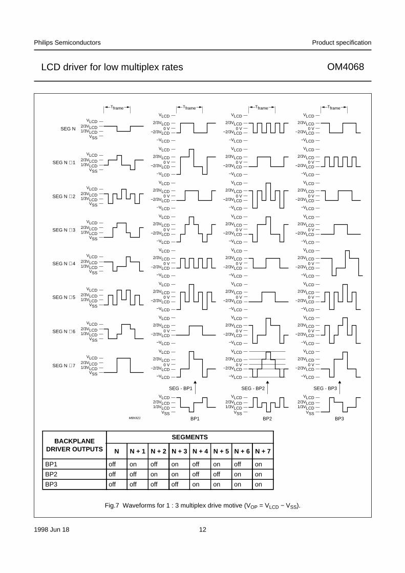
1 : 3 MULTIPLEX DRIVE MODE
When three backplanes are provided in the LCD, the 1 : 3 multiplex mode applies, as shown in Fig.7.
handbook, full pagewidth
MBK820
VLCD
1/2VLCDBP1
BP2
VSS
Tframe
SEG - BP1 SEG - BP2
Tframe Tframe
1/2VLCD
VLCD
0 V
−1/2VLCD
−VLCD
1/2VLCD
VLCD
0 V
−1/2VLCD
−VLCD
1/2VLCD
VLCD
0 V
−1/2VLCD
−VLCD
1/2VLCD
VLCD
0 V
−1/2VLCD
−VLCD
VLCD
1/2VLCDVSS
SEG N
SEG N + 1
SEG N + 2
SEG N + 3
VLCD
1/2VLCDVSS
VLCD
1/2VLCDVSS
VLCD
1/2VLCDVSS
VLCD
1/2VLCDVSS
1/2VLCD
VLCD
0 V
−1/2VLCD
−VLCD
1/2VLCD
VLCD
0 V
−1/2VLCD
−VLCD
1/2VLCD
VLCD
0 V
−1/2VLCD
−VLCD
1/2VLCD
VLCD
0 V
−1/2VLCD
−VLCD
Fig.6 Waveforms for 1 : 2 multiplex drive mode (VOP = VLCD − VSS).
BACKPLANEDRIVER OUTPUTS
SEGMENTS
SEG N SEG N + 1 SEG N + 2 SEG N + 3
BP1 off on off on
BP2 off off on on
1998 Jun 18 12
Philips Semiconductors Product specification
LCD driver for low multiplex rates OM4068
handbook, full pagewidth
MBK821
SEG N
SEG N + 1
SEG N + 2
SEG - BP3
SEG N + 3
SEG N + 4
SEG N + 5
SEG N + 6
SEG N + 7
2/3VLCD
−2/3VLCD
−VLCD
VLCD
0 V
2/3VLCD
−2/3VLCD
−VLCD
VLCD
0 V
2/3VLCD
−2/3VLCD
−VLCD
VLCD
0 V
2/3VLCD
−2/3VLCD
−VLCD
VLCD
0 V
2/3VLCD
−2/3VLCD
−VLCD
VLCD
0 V
2/3VLCD
−2/3VLCD
−VLCD
VLCD
0 V
2/3VLCD
−2/3VLCD
−VLCD
VLCD
0 V
2/3VLCD
−2/3VLCD
−VLCD
VLCD
0 V
2/3VLCD
−2/3VLCD
−VLCD
VLCD
0 V
2/3VLCD
−2/3VLCD
−VLCD
VLCD
0 V
2/3VLCD
−2/3VLCD
−VLCD
VLCD
0 V
2/3VLCD
−2/3VLCD
−VLCD
VLCD
0 V
2/3VLCD
−2/3VLCD
−VLCD
VLCD
0 V
2/3VLCD
−2/3VLCD
−VLCD
VLCD
0 V
2/3VLCD
VSS
VLCD
1/3VLCD
2/3VLCD
−2/3VLCD
−VLCD
VLCD
0 V
2/3VLCD
−2/3VLCD
−VLCD
VLCD
0 V
2/3VLCD
−2/3VLCD
−VLCD
VLCD
0 V
2/3VLCD
−2/3VLCD
−VLCD
VLCD
0 V
2/3VLCD
−2/3VLCD
−VLCD
VLCD
0 V
2/3VLCD
−2/3VLCD
−VLCD
VLCD
0 V
2/3VLCD
−2/3VLCD
−VLCD
VLCD
0 V
2/3VLCD
−2/3VLCD
−VLCD
VLCD
0 V
2/3VLCD
−2/3VLCD
−VLCD
VLCD
0 V
2/3VLCD
−2/3VLCD
−VLCD
VLCD
0 V
TframeTframe Tframe Tframe
SEG - BP2
BP2 BP3
2/3VLCD
VSS
VLCD
1/3VLCD
2/3VLCD
VSS
VLCD
1/3VLCD
2/3VLCD
VSS
VLCD
1/3VLCD
SEG - BP1
BP1
2/3VLCD
VSS
VLCD
1/3VLCD
2/3VLCD
VSS
VLCD
1/3VLCD
2/3VLCD
VSS
VLCD
1/3VLCD
2/3VLCD
VSS
VLCD
1/3VLCD
2/3VLCD
VSS
VLCD
1/3VLCD
2/3VLCD
VSS
VLCD
1/3VLCD
2/3VLCD
VSS
VLCD
1/3VLCD
Fig.7 Waveforms for 1 : 3 multiplex drive motive (VOP = VLCD − VSS).
BACKPLANEDRIVER OUTPUTS
SEGMENTS
N N + 1 N + 2 N + 3 N + 4 N + 5 N + 6 N + 7
BP1 off on off on off on off on
BP2 off off on on off off on on
BP3 off off off off on on on on
1998 Jun 18 13
Philips Semiconductors Product specification
LCD driver for low multiplex rates OM4068
Oscillator
The internal logic and the multi-level LCD drive signals ofthe OM4068 are generated by the built-in RC oscillator.No external components are required.
In order to minimize radio frequency interference, theoscillator operates with symmetrical and slew-rate limitedcapacitor charge/discharge.
The oscillator runs continuously once the power downstate after power-on has been left.
Interface to microprocessor unit: serial interface
A three-line bus structure enables serial unidirectionaldata transfer with microprocessors/microcontrollers.The three lines are a serial data input line (SDIN), a serialclock line (SCLK) and a data line enable (SCE). All inputsare CMOS compatible. These lines must always be in adefined state VSS or VDD. Floating inputs could damage thechip.
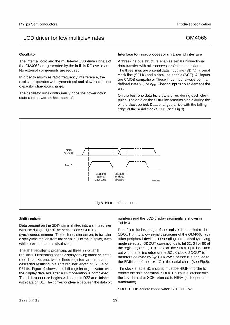
On the bus, one data bit is transferred during each clockpulse. The data on the SDIN line remains stable during thewhole clock period. Data changes arrive with the fallingedge of the serial clock SCLK (see Fig.8).
Fig.8 Bit transfer on bus.
handbook, full pagewidth
MBK822
data linestable;
data valid
changeof dataallowed
SDINSDOUT
SCLK
Shift register
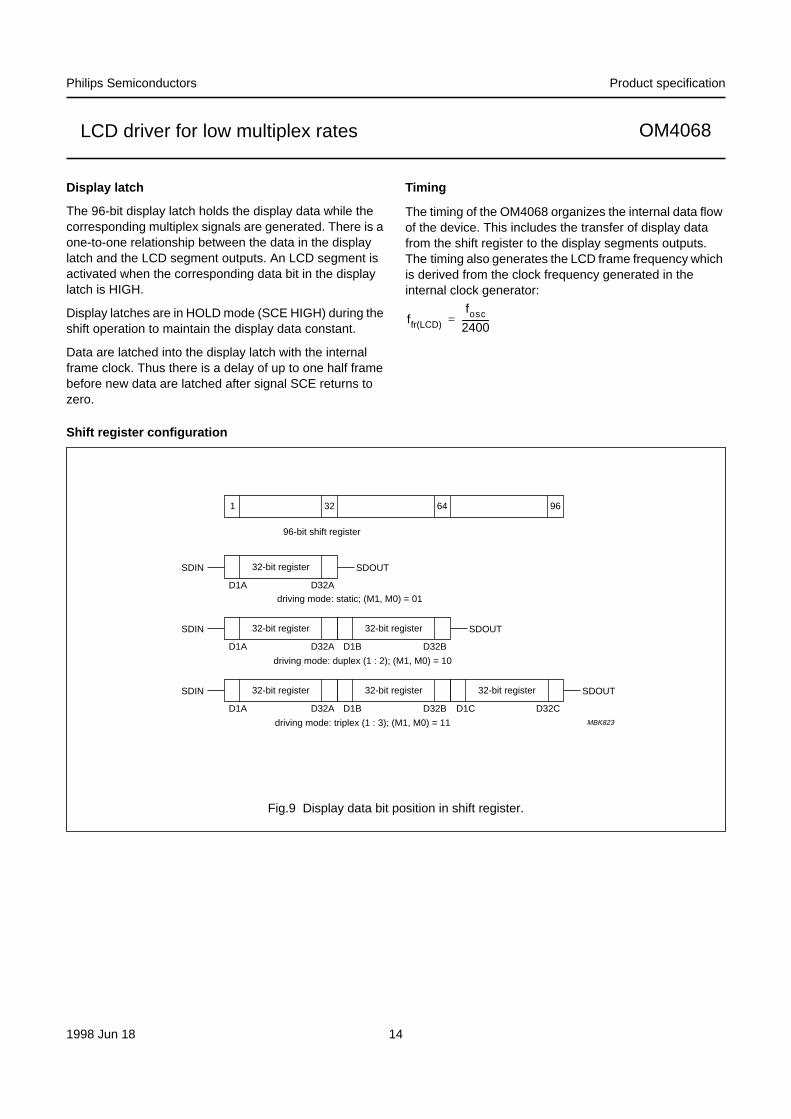
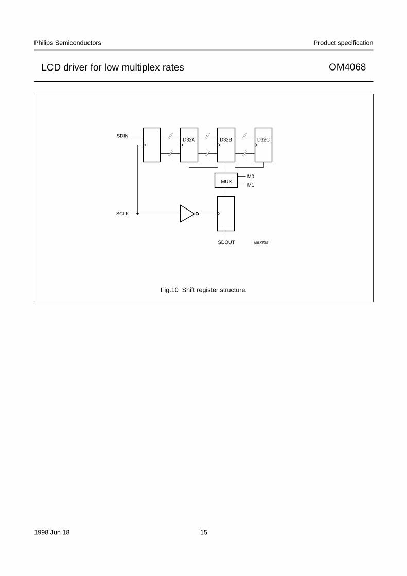
Data present on the SDIN pin is shifted into a shift registerwith the rising edge of the serial clock SCLK in asynchronous manner. The shift register serves to transferdisplay information from the serial bus to the (display) latchwhile previous data is displayed.
The shift register is organized as three 32-bit shiftregisters. Depending on the display driving mode selected(see Table 3), one, two or three registers are used andcascaded resulting in a shift register length of 32, 64 or96 bits. Figure 9 shows the shift register organization withthe display data bits after a shift operation is completed.The shift sequence begins with data bit D32 and finisheswith data bit D1. The correspondence between the data bit
numbers and the LCD display segments is shown inTable 4.
Data from the last stage of the register is supplied to theSDOUT pin to allow serial cascading of the OM4068 withother peripheral devices. Depending on the display drivingmode selected, SDOUT corresponds to bit 32, 64 or 96 ofthe register (see Fig.10). Data on the SDOUT pin is shiftedout with the falling edge of the SCLK clock. SDOUT istherefore delayed by 1⁄2SCLK cycle before it is applied tothe SDIN pin of the next IC in the serial chain (see Fig.8).
The clock enable SCE signal must be HIGH in order toenable the shift operation. SDOUT output is latched withthe last data after SCE returned to HIGH (shift operationterminated).
SDOUT is in 3-state mode when SCE is LOW.
1998 Jun 18 14
Philips Semiconductors Product specification
LCD driver for low multiplex rates OM4068
Display latch
The 96-bit display latch holds the display data while thecorresponding multiplex signals are generated. There is aone-to-one relationship between the data in the displaylatch and the LCD segment outputs. An LCD segment isactivated when the corresponding data bit in the displaylatch is HIGH.
Display latches are in HOLD mode (SCE HIGH) during theshift operation to maintain the display data constant.
Data are latched into the display latch with the internalframe clock. Thus there is a delay of up to one half framebefore new data are latched after signal SCE returns tozero.
Timing
The timing of the OM4068 organizes the internal data flowof the device. This includes the transfer of display datafrom the shift register to the display segments outputs.The timing also generates the LCD frame frequency whichis derived from the clock frequency generated in theinternal clock generator:
ffr(LCD)
fosc
2400-------------=
Shift register configuration
Fig.9 Display data bit position in shift register.
handbook, full pagewidth 1
D1A D32A
SDIN SDOUT
32
96-bit shift register
64 96
32-bit register
driving mode: static; (M1, M0) = 01
driving mode: duplex (1 : 2); (M1, M0) = 10
D1A D1BD32A D32B
SDIN 32-bit register SDOUT32-bit register
driving mode: triplex (1 : 3); (M1, M0) = 11
D1A D1BD32A D32B
SDIN 32-bit register 32-bit register
D1C D32CMBK823
SDOUT32-bit register
1998 Jun 18 15
Philips Semiconductors Product specification
LCD driver for low multiplex rates OM4068
Fig.10 Shift register structure.
handbook, full pagewidth
MUX
SDOUT
SDIND32A D32B D32C
SCLK
M0
M1
MBK825
1998 Jun 18 16
Philips Semiconductors Product specification
LCD driver for low multiplex rates OM4068
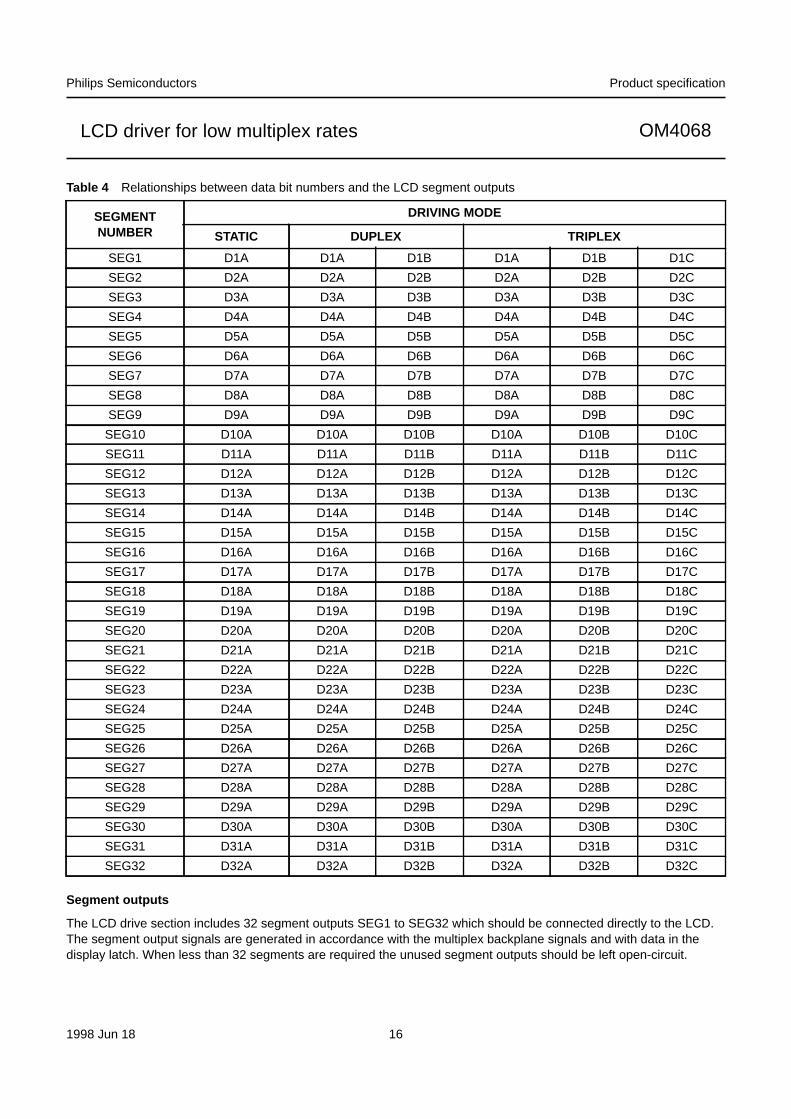
Table 4 Relationships between data bit numbers and the LCD segment outputs
Segment outputs
The LCD drive section includes 32 segment outputs SEG1 to SEG32 which should be connected directly to the LCD.The segment output signals are generated in accordance with the multiplex backplane signals and with data in thedisplay latch. When less than 32 segments are required the unused segment outputs should be left open-circuit.
SEGMENTNUMBER
DRIVING MODE
STATIC DUPLEX TRIPLEX
SEG1 D1A D1A D1B D1A D1B D1C
SEG2 D2A D2A D2B D2A D2B D2C
SEG3 D3A D3A D3B D3A D3B D3C
SEG4 D4A D4A D4B D4A D4B D4C
SEG5 D5A D5A D5B D5A D5B D5C
SEG6 D6A D6A D6B D6A D6B D6C
SEG7 D7A D7A D7B D7A D7B D7C
SEG8 D8A D8A D8B D8A D8B D8C
SEG9 D9A D9A D9B D9A D9B D9C
SEG10 D10A D10A D10B D10A D10B D10C
SEG11 D11A D11A D11B D11A D11B D11C
SEG12 D12A D12A D12B D12A D12B D12C
SEG13 D13A D13A D13B D13A D13B D13C
SEG14 D14A D14A D14B D14A D14B D14C
SEG15 D15A D15A D15B D15A D15B D15C
SEG16 D16A D16A D16B D16A D16B D16C
SEG17 D17A D17A D17B D17A D17B D17C
SEG18 D18A D18A D18B D18A D18B D18C
SEG19 D19A D19A D19B D19A D19B D19C
SEG20 D20A D20A D20B D20A D20B D20C
SEG21 D21A D21A D21B D21A D21B D21C
SEG22 D22A D22A D22B D22A D22B D22C
SEG23 D23A D23A D23B D23A D23B D23C
SEG24 D24A D24A D24B D24A D24B D24C
SEG25 D25A D25A D25B D25A D25B D25C
SEG26 D26A D26A D26B D26A D26B D26C
SEG27 D27A D27A D27B D27A D27B D27C
SEG28 D28A D28A D28B D28A D28B D28C
SEG29 D29A D29A D29B D29A D29B D29C
SEG30 D30A D30A D30B D30A D30B D30C
SEG31 D31A D31A D31B D31A D31B D31C
SEG32 D32A D32A D32B D32A D32B D32C
1998 Jun 18 17
Philips Semiconductors Product specification
LCD driver for low multiplex rates OM4068
Backplane outputs
The LCD drive section includes three backplane outputs (BP1 to BP3) which should be connected directly to the LCD.The backplane output signals are generated in accordance with the selected LCD drive mode. If less than threebackplane outputs are required the unused outputs should be left open-circuit. In 1 : 2 multiplex drive mode, BP3 is setto 1⁄2VLCD. In static drive mode BP3 and BP2 are set to VSS.
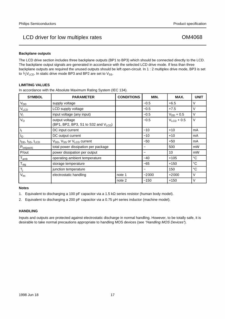
LIMITING VALUESIn accordance with the Absolute Maximum Rating System (IEC 134).
Notes
1. Equivalent to discharging a 100 pF capacitor via a 1.5 kΩ series resistor (human body model).
2. Equivalent to discharging a 200 pF capacitor via a 0.75 µH series inductor (machine model).
HANDLING
Inputs and outputs are protected against electrostatic discharge in normal handling. However, to be totally safe, it isdesirable to take normal precautions appropriate to handling MOS devices (see “Handling MOS Devices”).
SYMBOL PARAMETER CONDITIONS MIN. MAX. UNIT
VDD supply voltage −0.5 +6.5 V
VLCD LCD supply voltage −0.5 +7.5 V
VI input voltage (any input) −0.5 VDD + 0.5 V
VO output voltage(BP1, BP2, BP3, S1 to S32 and VLCD)
−0.5 VLCD + 0.5 V
II DC input current −10 +10 mA
IO DC output current −10 +10 mA
IDD, ISS, ILCD VDD, VSS or VLCD current −50 +50 mA
Ptot(pack) total power dissipation per package − 500 mW
P/out power dissipation per output − 10 mW
Tamb operating ambient temperature −40 +105 °CTstg storage temperature −65 +150 °CTj junction temperature − 150 °CVes electrostatic handling note 1 −2000 +2000 V
note 2 −150 +150 V
1998 Jun 18 18
Philips Semiconductors Product specification
LCD driver for low multiplex rates OM4068
DC CHARACTERISTICSVDD = 2.5 to 5.5 V; VSS = 0 V; VLCD = 3.5 to 6.5 V; Tamb = −40 to +105 °C; unless otherwise specified.
Notes
1. Power-down state. After power-on the chip is in power-down state as long as the serial clock is not activated. Duringpower-down all static currents are switched off except the power-on reset block.
2. Output SDOUT is open-circuit; inputs at VDD or VSS; bus inactive.
3. Drive mode: static, duplex and triplex.
4. LCD outputs are open-circuit, CL = 50 pF typical, inputs at VDD or VSS; bus inactive.
5. Resets all logic when VDD < VPOR.
6. Resistance of output terminal (S1 to S32 and BP1, BP2 and BP3) with a load current of 20 µA; outputs measuredone at a time.
7. LCD outputs open-circuits.
SYMBOL PARAMETER CONDITIONS MIN. TYP. MAX. UNIT
Supplies
VDD supply voltage VSS + 2.5 − 5.5 V
VLCD LCD supply voltage VSS + 3.5 − 6.5 V
IDD supply current power-down state;note 1
− 4 10 µA
normal mode;fosc = intern;notes 2 and 3
− 12 25 µA
ILCD VLCD current power-down state;note 1
− − 1.5 µA
normal mode;fosc = intern;notes 3 and 4
− − 40 µA
VPOR power-on reset voltage level note 5 0.8 1.25 1.6 V
Logic
VIL LOW-level input voltage VSS − 0.3VDD V
VIH HIGH-level input voltage 0.7VDD − VDD V
IOL LOW-level output current (SDOUT) VOL = 0.5 V; VDD = 5 V 1.0 − − mA
IOH HIGH-level output current (SDOUT) VOH = VDD − 0.5 V;VDD = 5 V
− − −1 mA
Ipu pull-up current M1 and M0 VI = VSS 0.04 0.15 1 µA
IL leakage current VI = VDD or VSS −1 − +1 µA
Segment and backplane outputs
R(o)seg segment output resistanceSEG1 to SEG32
note 6 − 15 40 kΩ
R(o)back backplane output resistanceBP1 to BP3
note 6 − 15 40 kΩ
Vseg(bias)(tol) bias tolerance SEG1 to SEG32 note 7 −100 0 +100 mV
Vback(bias)(tol) bias tolerance BP1, BP2 and BP3 note 7 −100 0 +100 mV
1998 Jun 18 19
Philips Semiconductors Product specification
LCD driver for low multiplex rates OM4068
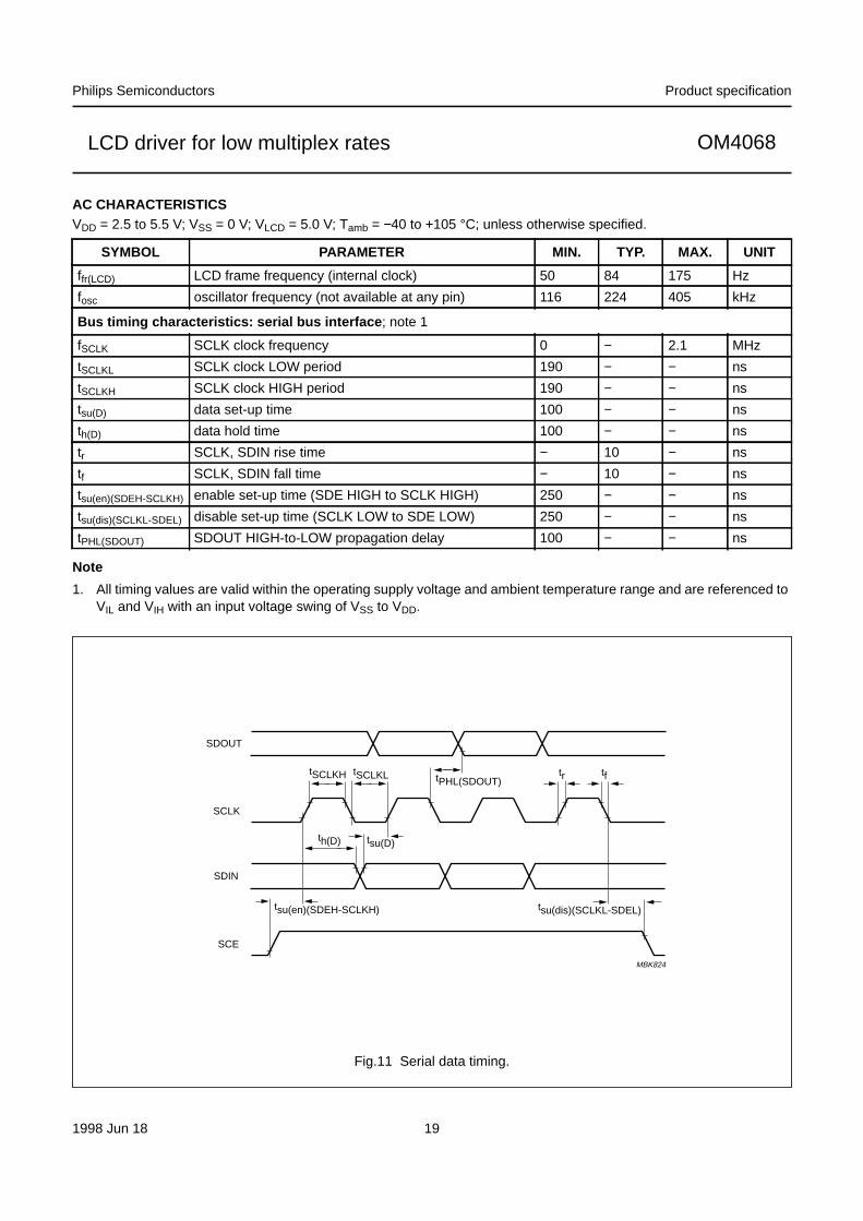
AC CHARACTERISTICSVDD = 2.5 to 5.5 V; VSS = 0 V; VLCD = 5.0 V; Tamb = −40 to +105 °C; unless otherwise specified.
Note
1. All timing values are valid within the operating supply voltage and ambient temperature range and are referenced toVIL and VIH with an input voltage swing of VSS to VDD.
SYMBOL PARAMETER MIN. TYP. MAX. UNIT
ffr(LCD) LCD frame frequency (internal clock) 50 84 175 Hz
fosc oscillator frequency (not available at any pin) 116 224 405 kHz
Bus timing characteristics: serial bus interface ; note 1
fSCLK SCLK clock frequency 0 − 2.1 MHz
tSCLKL SCLK clock LOW period 190 − − ns
tSCLKH SCLK clock HIGH period 190 − − ns
tsu(D) data set-up time 100 − − ns
th(D) data hold time 100 − − ns
tr SCLK, SDIN rise time − 10 − ns
tf SCLK, SDIN fall time − 10 − ns
tsu(en)(SDEH-SCLKH) enable set-up time (SDE HIGH to SCLK HIGH) 250 − − ns
tsu(dis)(SCLKL-SDEL) disable set-up time (SCLK LOW to SDE LOW) 250 − − ns
tPHL(SDOUT) SDOUT HIGH-to-LOW propagation delay 100 − − ns
Fig.11 Serial data timing.
handbook, full pagewidth
MBK824
tSCLKH tSCLKL
th(D)
tsu(en)(SDEH-SCLKH) tsu(dis)(SCLKL-SDEL)
tsu(D)
tr tftPHL(SDOUT)
SDOUT
SCLK
SDIN
SCE
1998 Jun 18 20
Philips Semiconductors Product specification
LCD driver for low multiplex rates OM4068
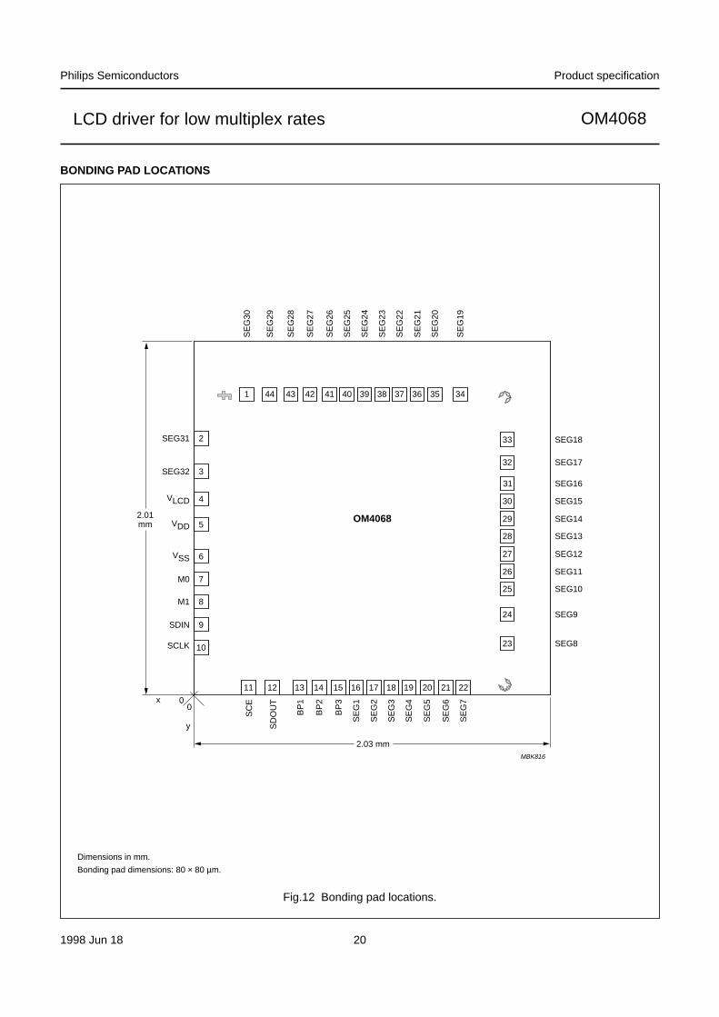
BONDING PAD LOCATIONS
Fig.12 Bonding pad locations.
Dimensions in mm.
Bonding pad dimensions: 80 × 80 µm.
handbook, full pagewidth
MBK816
2.03 mm
2.01mm
x
y
00
2SEG31
4VLCD
5VDD
6VSS
7M0
8M1
9SDIN
10
11
SC
E
12
SD
OU
T
13
BP
1
14
BP
2
15
BP
3
16
SE
G1
17
SE
G2
18
SE
G3
19
SE
G4
20
SE
G5
21
SE
G6
22
SE
G7
23 SEG8
24 SEG9
25 SEG10
26 SEG11
27 SEG12
28 SEG13
29 SEG14
30 SEG15
31 SEG16
32 SEG17
33 SEG18
34
SE
G19
35
SE
G20
36
SE
G21
37S
EG
2238
SE
G23
39
SE
G24
40
SE
G25
41
SE
G26
42
SE
G27
43
SE
G28
44
SE
G29
1
SE
G30
SCLK
3SEG32
OM4068
1998 Jun 18 21
Philips Semiconductors Product specification
LCD driver for low multiplex rates OM4068
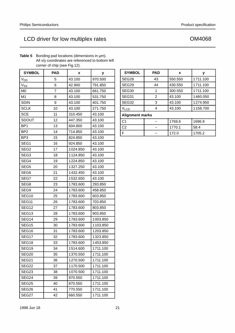
Table 5 Bonding pad locations (dimensions in µm).All x/y coordinates are referenced to bottom leftcorner of chip (see Fig.12).
SYMBOL PAD x y
VDD 5 43.100 970.500
VSS 6 42.900 791.850
M0 7 43.100 661.750
M1 8 43.100 531.750
SDIN 9 43.100 401.750
SCLK 10 43.100 271.750
SCE 11 310.450 43.100
SDOUT 12 447.350 43.100
BP1 13 604.800 43.100
BP2 14 714.850 43.100
BP3 15 824.850 43.100
SEG1 16 924.850 43.100
SEG2 17 1024.850 43.100
SEG3 18 1124.850 43.100
SEG4 19 1224.850 43.100
SEG5 20 1327.250 43.100
SEG6 21 1432.450 43.100
SEG7 22 1532.650 43.100
SEG8 23 1783.600 293.850
SEG9 24 1783.600 458.850
SEG10 25 1783.600 603.850
SEG11 26 1783.600 703.850
SEG12 27 1783.600 803.850
SEG13 28 1783.600 903.850
SEG14 29 1783.600 1003.850
SEG15 30 1783.600 1103.850
SEG16 31 1783.600 1203.850
SEG17 32 1783.600 1323.850
SEG18 33 1783.600 1453.850
SEG19 34 1514.600 1711.100
SEG20 35 1370.550 1711.100
SEG21 36 1270.500 1711.100
SEG22 37 1170.500 1711.100
SEG23 38 1070.500 1711.100
SEG24 39 970.550 1711.100
SEG25 40 870.550 1711.100
SEG26 41 770.550 1711.100
SEG27 42 660.550 1711.100
SEG28 43 550.550 1711.100
SEG29 44 430.550 1711.100
SEG30 1 300.550 1711.100
SEG31 2 43.100 1460.050
SEG32 3 43.100 1274.950
VLCD 4 43.100 1158.700
Alignment marks
C1 − 1769.6 1696.9
C2 − 1770.1 58.4
F − 172.0 1705.2
SYMBOL PAD x y

1998 Jun 18 22
Philips Semiconductors Product specification
LCD driver for low multiplex rates OM4068
PACKAGE OUTLINES
UNIT A1 A2 A3 bp c E(1) e HE L Lp Zywv θ
REFERENCESOUTLINEVERSION
EUROPEANPROJECTION ISSUE DATE
IEC JEDEC EIAJ
mm 0.250.05
1.851.65 0.25
0.400.20
0.250.14
10.19.9 0.8 1.3
12.912.3
1.20.8
100
o
o0.15 0.10.15
DIMENSIONS (mm are the original dimensions)
Note
1. Plastic or metal protrusions of 0.25 mm maximum per side are not included.
0.950.55
SOT307-295-02-0497-08-01
D(1) (1)(1)
10.19.9
HD
12.912.3
EZ
1.20.8
D
e
E
B
11
c
EH
D
ZD
A
ZE
e
v M A
X
1
44
34
33 23
22
12
y
θ
A1A
Lp
detail X
L
(A )3A2
pin 1 index
DH v M B
bp
bp
w M
w M
0 2.5 5 mm
scale
QFP44: plastic quad flat package; 44 leads (lead length 1.3 mm); body 10 x 10 x 1.75 mm SOT307-2
Amax.
2.10
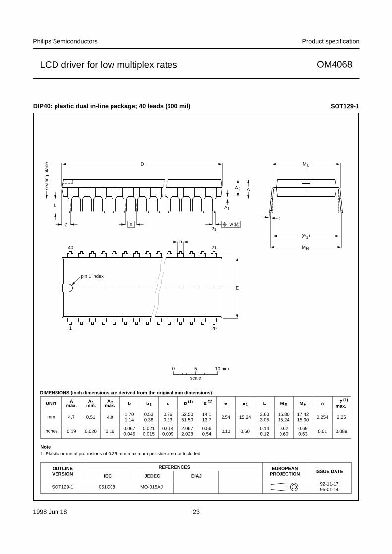
1998 Jun 18 23
Philips Semiconductors Product specification
LCD driver for low multiplex rates OM4068
UNIT Amax.
1 2 b1 c D E e MHL
REFERENCESOUTLINEVERSION
EUROPEANPROJECTION ISSUE DATE
IEC JEDEC EIAJ
mm
inches
DIMENSIONS (inch dimensions are derived from the original mm dimensions)
SOT129-192-11-1795-01-14
A min.
A max. b Z
max.wMEe1
1.701.14
0.530.38
0.360.23
52.5051.50
14.113.7
3.603.05 0.2542.54 15.24
15.8015.24
17.4215.90 2.254.7 0.51 4.0
0.0670.045
0.0210.015
0.0140.009
2.0672.028
0.560.54
0.140.12 0.010.10 0.60
0.620.60
0.690.63 0.089 0.19 0.020 0.16
051G08 MO-015AJ
MH
c
(e )1
ME
A
L
seat
ing
plan
e
A1
w Mb1
e
D
A2
Z
40
1
21
20
b
E
pin 1 index
0 5 10 mm
scale
Note
1. Plastic or metal protrusions of 0.25 mm maximum per side are not included.
(1)(1)(1)
DIP40: plastic dual in-line package; 40 leads (600 mil) SOT129-1
1998 Jun 18 24
Philips Semiconductors Product specification
LCD driver for low multiplex rates OM4068
SOLDERING
Introduction
There is no soldering method that is ideal for all ICpackages. Wave soldering is often preferred whenthrough-hole and surface mounted components are mixedon one printed-circuit board. However, wave soldering isnot always suitable for surface mounted ICs, or forprinted-circuits with high population densities. In thesesituations reflow soldering is often used.
This text gives a very brief insight to a complex technology.A more in-depth account of soldering ICs can be found inour “Data Handbook IC26; Integrated Circuit Packages”(order code 9398 652 90011).
DIP
SOLDERING BY DIPPING OR BY WAVE
The maximum permissible temperature of the solder is260 °C; solder at this temperature must not be in contactwith the joint for more than 5 seconds. The total contacttime of successive solder waves must not exceed5 seconds.
The device may be mounted up to the seating plane, butthe temperature of the plastic body must not exceed thespecified maximum storage temperature (Tstg max). If theprinted-circuit board has been pre-heated, forced coolingmay be necessary immediately after soldering to keep thetemperature within the permissible limit.
REPAIRING SOLDERED JOINTS
Apply a low voltage soldering iron (less than 24 V) to thelead(s) of the package, below the seating plane or notmore than 2 mm above it. If the temperature of thesoldering iron bit is less than 300 °C it may remain incontact for up to 10 seconds. If the bit temperature isbetween 300 and 400 °C, contact may be up to 5 seconds.
QFP
REFLOW SOLDERING
Reflow soldering techniques are suitable for all QFPpackages.
The choice of heating method may be influenced by largerplastic QFP packages (44 leads, or more). If infrared orvapour phase heating is used and the large packages arenot absolutely dry (less than 0.1% moisture content byweight), vaporization of the small amount of moisture inthem can cause cracking of the plastic body. For details,refer to the Drypack information in the “Data HandbookIC26; Integrated Circuit Packages; Section: PackingMethods”.
Reflow soldering requires solder paste (a suspension offine solder particles, flux and binding agent) to be appliedto the printed-circuit board by screen printing, stencilling orpressure-syringe dispensing before package placement.
Several methods exist for reflowing; for example,infrared/convection heating in a conveyor type oven.Throughput times (preheating, soldering and cooling) varybetween 50 and 300 seconds depending on heatingmethod. Typical reflow peak temperatures range from215 to 250 °C.
WAVE SOLDERING
Wave soldering is not recommended for QFP packages.This is because of the likelihood of solder bridging due toclosely-spaced leads and the possibility of incompletesolder penetration in multi-lead devices.
If wave soldering cannot be avoided, for QFPpackages with a pitch (e) larger than 0.5 mm, thefollowing conditions must be observed:
• A double-wave (a turbulent wave with high upwardpressure followed by a smooth laminar wave)soldering technique should be used.
• The footprint must be at an angle of 45 ° to the boarddirection and must incorporate solder thievesdownstream and at the side corners.
CAUTION
Wave soldering is NOT applicable for all QFPpackages with a pitch (e) equal or less than 0.5 mm.
1998 Jun 18 25
Philips Semiconductors Product specification
LCD driver for low multiplex rates OM4068
During placement and before soldering, the package mustbe fixed with a droplet of adhesive. The adhesive can beapplied by screen printing, pin transfer or syringedispensing. The package can be soldered after theadhesive is cured.
Maximum permissible solder temperature is 260 °C, andmaximum duration of package immersion in solder is10 seconds, if cooled to less than 150 °C within6 seconds. Typical dwell time is 4 seconds at 250 °C.
A mildly-activated flux will eliminate the need for removalof corrosive residues in most applications.
REPAIRING SOLDERED JOINTS
Fix the component by first soldering two diagonally-opposite end leads. Use only a low voltage soldering iron(less than 24 V) applied to the flat part of the lead. Contacttime must be limited to 10 seconds at up to 300 °C. Whenusing a dedicated tool, all other leads can be soldered inone operation within 2 to 5 seconds between270 and 320 °C.
DEFINITIONS
LIFE SUPPORT APPLICATIONS
These products are not designed for use in life support appliances, devices, or systems where malfunction of theseproducts can reasonably be expected to result in personal injury. Philips customers using or selling these products foruse in such applications do so at their own risk and agree to fully indemnify Philips for any damages resulting from suchimproper use or sale.
Data sheet status
Objective specification This data sheet contains target or goal specifications for product development.
Preliminary specification This data sheet contains preliminary data; supplementary data may be published later.
Product specification This data sheet contains final product specifications.
Limiting values
Limiting values given are in accordance with the Absolute Maximum Rating System (IEC 134). Stress above one ormore of the limiting values may cause permanent damage to the device. These are stress ratings only and operationof the device at these or at any other conditions above those given in the Characteristics sections of the specificationis not implied. Exposure to limiting values for extended periods may affect device reliability.
Application information
Where application information is given, it is advisory and does not form part of the specification.
1998 Jun 18 26
Philips Semiconductors Product specification
LCD driver for low multiplex rates OM4068
NOTES

1998 Jun 18 27
Philips Semiconductors Product specification
LCD driver for low multiplex rates OM4068
NOTES

Internet: http://www.semiconductors.philips.com
Philips Semiconductors – a worldwide company
© Philips Electronics N.V. 1998 SCA60
All rights are reserved. Reproduction in whole or in part is prohibited without the prior written consent of the copyright owner.
The information presented in this document does not form part of any quotation or contract, is believed to be accurate and reliable and may be changedwithout notice. No liability will be accepted by the publisher for any consequence of its use. Publication thereof does not convey nor imply any licenseunder patent- or other industrial or intellectual property rights.
Middle East: see Italy
Netherlands: Postbus 90050, 5600 PB EINDHOVEN, Bldg. VB,Tel. +31 40 27 82785, Fax. +31 40 27 88399
New Zealand: 2 Wagener Place, C.P.O. Box 1041, AUCKLAND,Tel. +64 9 849 4160, Fax. +64 9 849 7811
Norway: Box 1, Manglerud 0612, OSLO,Tel. +47 22 74 8000, Fax. +47 22 74 8341
Pakistan: see Singapore
Philippines: Philips Semiconductors Philippines Inc.,106 Valero St. Salcedo Village, P.O. Box 2108 MCC, MAKATI,Metro MANILA, Tel. +63 2 816 6380, Fax. +63 2 817 3474
Poland: Ul. Lukiska 10, PL 04-123 WARSZAWA,Tel. +48 22 612 2831, Fax. +48 22 612 2327
Portugal: see Spain
Romania: see Italy
Russia: Philips Russia, Ul. Usatcheva 35A, 119048 MOSCOW,Tel. +7 095 755 6918, Fax. +7 095 755 6919
Singapore: Lorong 1, Toa Payoh, SINGAPORE 319762,Tel. +65 350 2538, Fax. +65 251 6500
Slovakia: see Austria
Slovenia: see Italy
South Africa: S.A. PHILIPS Pty Ltd., 195-215 Main Road Martindale,2092 JOHANNESBURG, P.O. Box 7430 Johannesburg 2000,Tel. +27 11 470 5911, Fax. +27 11 470 5494
South America: Al. Vicente Pinzon, 173, 6th floor,04547-130 SÃO PAULO, SP, Brazil,Tel. +55 11 821 2333, Fax. +55 11 821 2382
Spain: Balmes 22, 08007 BARCELONA,Tel. +34 93 301 6312, Fax. +34 93 301 4107
Sweden: Kottbygatan 7, Akalla, S-16485 STOCKHOLM,Tel. +46 8 5985 2000, Fax. +46 8 5985 2745
Switzerland: Allmendstrasse 140, CH-8027 ZÜRICH,Tel. +41 1 488 2741 Fax. +41 1 488 3263
Taiwan: Philips Semiconductors, 6F, No. 96, Chien Kuo N. Rd., Sec. 1,TAIPEI, Taiwan Tel. +886 2 2134 2865, Fax. +886 2 2134 2874
Thailand: PHILIPS ELECTRONICS (THAILAND) Ltd.,209/2 Sanpavuth-Bangna Road Prakanong, BANGKOK 10260,Tel. +66 2 745 4090, Fax. +66 2 398 0793
Turkey: Talatpasa Cad. No. 5, 80640 GÜLTEPE/ISTANBUL,Tel. +90 212 279 2770, Fax. +90 212 282 6707
Ukraine : PHILIPS UKRAINE, 4 Patrice Lumumba str., Building B, Floor 7,252042 KIEV, Tel. +380 44 264 2776, Fax. +380 44 268 0461
United Kingdom: Philips Semiconductors Ltd., 276 Bath Road, Hayes,MIDDLESEX UB3 5BX, Tel. +44 181 730 5000, Fax. +44 181 754 8421
United States: 811 East Arques Avenue, SUNNYVALE, CA 94088-3409,Tel. +1 800 234 7381
Uruguay: see South America
Vietnam: see Singapore
Yugoslavia: PHILIPS, Trg N. Pasica 5/v, 11000 BEOGRAD,Tel. +381 11 625 344, Fax.+381 11 635 777
For all other countries apply to: Philips Semiconductors,International Marketing & Sales Communications, Building BE-p, P.O. Box 218,5600 MD EINDHOVEN, The Netherlands, Fax. +31 40 27 24825
Argentina: see South America
Australia: 34 Waterloo Road, NORTH RYDE, NSW 2113,Tel. +61 2 9805 4455, Fax. +61 2 9805 4466
Austria: Computerstr. 6, A-1101 WIEN, P.O. Box 213, Tel. +43 160 1010,Fax. +43 160 101 1210
Belarus: Hotel Minsk Business Center, Bld. 3, r. 1211, Volodarski Str. 6,220050 MINSK, Tel. +375 172 200 733, Fax. +375 172 200 773
Belgium: see The Netherlands
Brazil: see South America
Bulgaria: Philips Bulgaria Ltd., Energoproject, 15th floor,51 James Bourchier Blvd., 1407 SOFIA,Tel. +359 2 689 211, Fax. +359 2 689 102
Canada: PHILIPS SEMICONDUCTORS/COMPONENTS,Tel. +1 800 234 7381
China/Hong Kong: 501 Hong Kong Industrial Technology Centre,72 Tat Chee Avenue, Kowloon Tong, HONG KONG,Tel. +852 2319 7888, Fax. +852 2319 7700
Colombia: see South America
Czech Republic: see Austria
Denmark: Prags Boulevard 80, PB 1919, DK-2300 COPENHAGEN S,Tel. +45 32 88 2636, Fax. +45 31 57 0044
Finland: Sinikalliontie 3, FIN-02630 ESPOO,Tel. +358 9 615800, Fax. +358 9 61580920
France: 51 Rue Carnot, BP317, 92156 SURESNES Cedex,Tel. +33 1 40 99 6161, Fax. +33 1 40 99 6427
Germany: Hammerbrookstraße 69, D-20097 HAMBURG,Tel. +49 40 23 53 60, Fax. +49 40 23 536 300
Greece: No. 15, 25th March Street, GR 17778 TAVROS/ATHENS,Tel. +30 1 4894 339/239, Fax. +30 1 4814 240
Hungary: see Austria
India: Philips INDIA Ltd, Band Box Building, 2nd floor,254-D, Dr. Annie Besant Road, Worli, MUMBAI 400 025,Tel. +91 22 493 8541, Fax. +91 22 493 0966
Indonesia: PT Philips Development Corporation, Semiconductors Division,Gedung Philips, Jl. Buncit Raya Kav.99-100, JAKARTA 12510,Tel. +62 21 794 0040 ext. 2501, Fax. +62 21 794 0080
Ireland: Newstead, Clonskeagh, DUBLIN 14,Tel. +353 1 7640 000, Fax. +353 1 7640 200
Israel: RAPAC Electronics, 7 Kehilat Saloniki St, PO Box 18053,TEL AVIV 61180, Tel. +972 3 645 0444, Fax. +972 3 649 1007
Italy: PHILIPS SEMICONDUCTORS, Piazza IV Novembre 3,20124 MILANO, Tel. +39 2 6752 2531, Fax. +39 2 6752 2557
Japan: Philips Bldg 13-37, Kohnan 2-chome, Minato-ku,TOKYO 108-8507, Tel. +81 3 3740 5130, Fax. +81 3 3740 5077
Korea: Philips House, 260-199 Itaewon-dong, Yongsan-ku, SEOUL,Tel. +82 2 709 1412, Fax. +82 2 709 1415
Malaysia: No. 76 Jalan Universiti, 46200 PETALING JAYA, SELANGOR,Tel. +60 3 750 5214, Fax. +60 3 757 4880
Mexico: 5900 Gateway East, Suite 200, EL PASO, TEXAS 79905,Tel. +9-5 800 234 7381
Printed in The Netherlands 415106/1200/01/pp28 Date of release: 1998 Jun 18 Document order number: 9397 750 03802