PCB/Substrate Finishing Overview
50
1 CIRCUITRY SOLUTIONS SEMICONDUCTOR SOLUTIONS ASSEMBLY SOLUTIONS July 21/22, 2021 John Swanson, Director of Final Finishes PCB/Substrate Finishing Overview Watch the recorded webinar: • https://youtu.be/S0Ejj5wIttE OR • http://thor.inemi.org/webdownload/2021/BdAssy- Tech_Topics/Surface_Finishes.mp4
Transcript of PCB/Substrate Finishing Overview

1CIRCUITRY SOLUTIONS SEMICONDUCTOR SOLUTIONS ASSEMBLY SOLUTIONS
July 21/22, 2021
John Swanson, Director of Final Finishes
PCB/Substrate Finishing Overview
Watch the recorded webinar:• https://youtu.be/S0Ejj5wIttE
OR• http://thor.inemi.org/webdownload/2021/BdAssy-
Tech_Topics/Surface_Finishes.mp4
2CIRCUITRY SOLUTIONS SEMICONDUCTOR SOLUTIONS ASSEMBLY SOLUTIONS
PCB Surface Finish Overview
Surface Finish deployment
ranked by surface area
OSP greatest
Imm Tin
ENIG
Silver
ENEPIG least
* Consult process vendor for specifics
** dependent on specifics of assembly temperature, time, etc.
3CIRCUITRY SOLUTIONS SEMICONDUCTOR SOLUTIONS ASSEMBLY SOLUTIONS
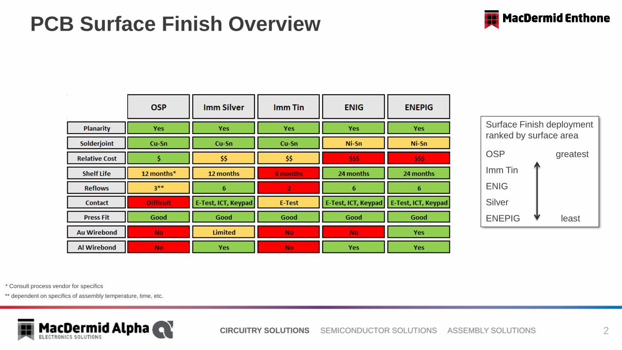
Assembly/reflow considerations
▪ Complete PCB / device assembly commonly
involves multiple exposures to significant heat
cycles
▪ Assembly conditions (time, temperature,
environment) will vary by application.
▪ Surface finishes vary in their performance and
“resilience” to these conditions
▪ Subsequent longer term “performance” may be a
consideration
▪ Tradeoffs of “fit versus cost” are considered
4CIRCUITRY SOLUTIONS SEMICONDUCTOR SOLUTIONS ASSEMBLY SOLUTIONS
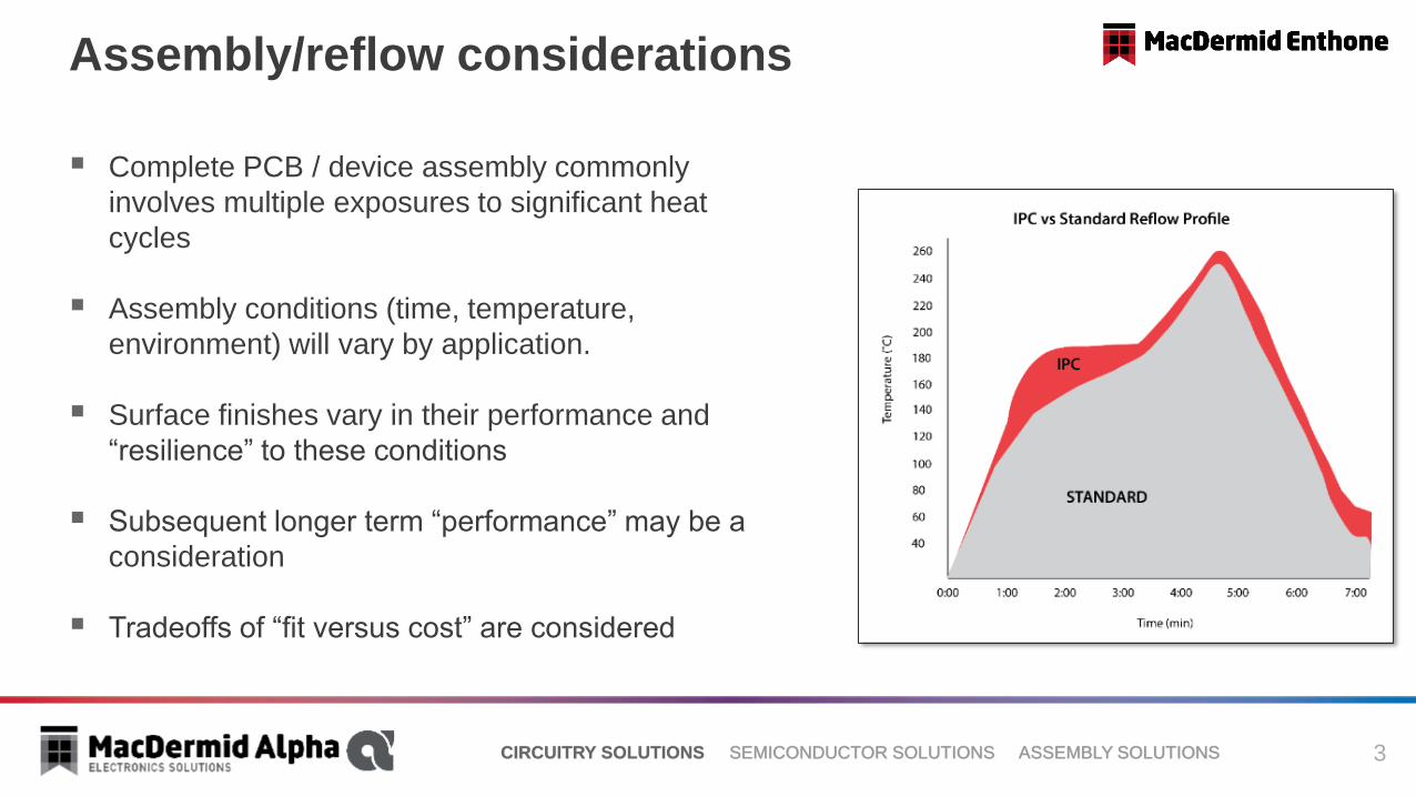
Characteristics for Consideration
Coating
thickness
Process
note
Coating change
with heat + time
Soldering
mechanism
Solder joint
copper
OSP(Organic Solderability Preservative)
~ 0.3 micron
organic molecule
(azole) bond with copper
general organic
degradation
organic breakdown in flux
and dissolution in solder
Tin/Copper
copper
Immersion Silver
~ 0.25 micron
immersion plating
minimal oxidation
rapid silver dissolution
in solder
Tin/Copper
copper
Immersion Tin
~ 1.0 micron
immersion plating
thin tin oxide +
tin/copper alloy growth
rapid tin dissolution in
solder
Tin/Copper
copper
ENIG(Electroless Nickel Immersion Gold)
0.04 – 0.10 micron Au
3-6 micron Ni*
electroless +
immersion plating
minimal oxidation
rapid gold dissolution in
solder, partial nickel….
Tin/Nickel
copper
ENEPIG(Electroless Nickel Electroless Palladium
Immersion Gold)
0.03 – 0.07 micron Au
0.05 – 0.3 micron Pd
3-6 micron Ni*
electroless +
immersion plating
minimal oxidation
rapid gold and palladium
dissolution, partial nickel….
Tin/Nickel
* Thin nickel, < 0.5 micron, in some specialty applications
5CIRCUITRY SOLUTIONS SEMICONDUCTOR SOLUTIONS ASSEMBLY SOLUTIONS
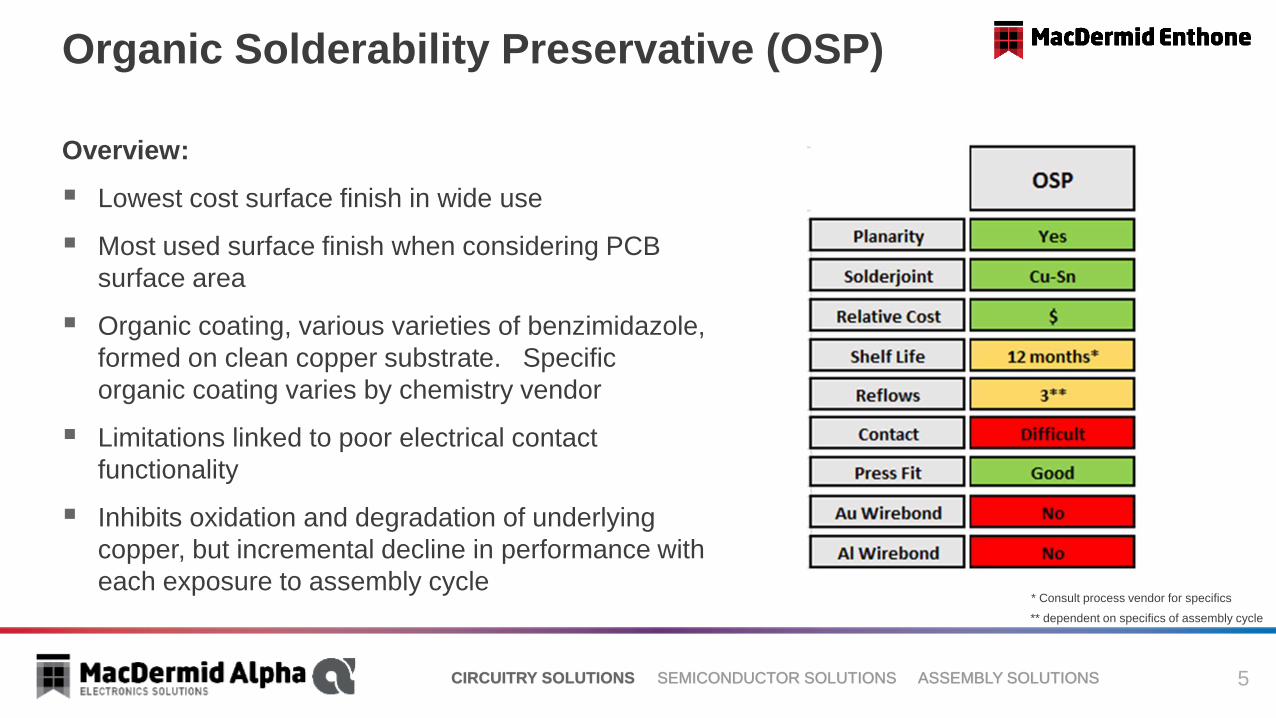
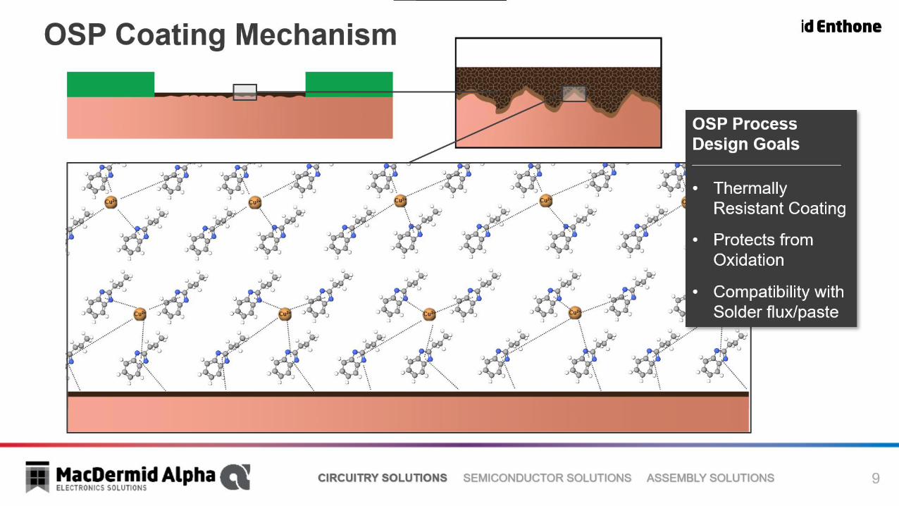
Organic Solderability Preservative (OSP)
Overview:
▪ Lowest cost surface finish in wide use
▪ Most used surface finish when considering PCB
surface area
▪ Organic coating, various varieties of benzimidazole,
formed on clean copper substrate. Specific
organic coating varies by chemistry vendor
▪ Limitations linked to poor electrical contact
functionality
▪ Inhibits oxidation and degradation of underlying
copper, but incremental decline in performance with
each exposure to assembly cycle* Consult process vendor for specifics
** dependent on specifics of assembly cycle

6CIRCUITRY SOLUTIONS SEMICONDUCTOR SOLUTIONS ASSEMBLY SOLUTIONS
Engineering of OSP
Consideration regarding coating and
process:
▪ Ease of use, stability of OSP
processing chemistry
▪ Thickness capability
▪ Permeability to air
▪ Heat stability of coating
▪ Compatibility with flux/pastePCB Pad Copper Surface
OSP Coating
Organic Molecule with
specific chemical,
physical, and electrical
properities
Variation may exist
among process
suppliers
OSP
Deposit
Hot assembly conditions cause degradation of basic
organic molecule, thin coating.

7CIRCUITRY SOLUTIONS SEMICONDUCTOR SOLUTIONS ASSEMBLY SOLUTIONS
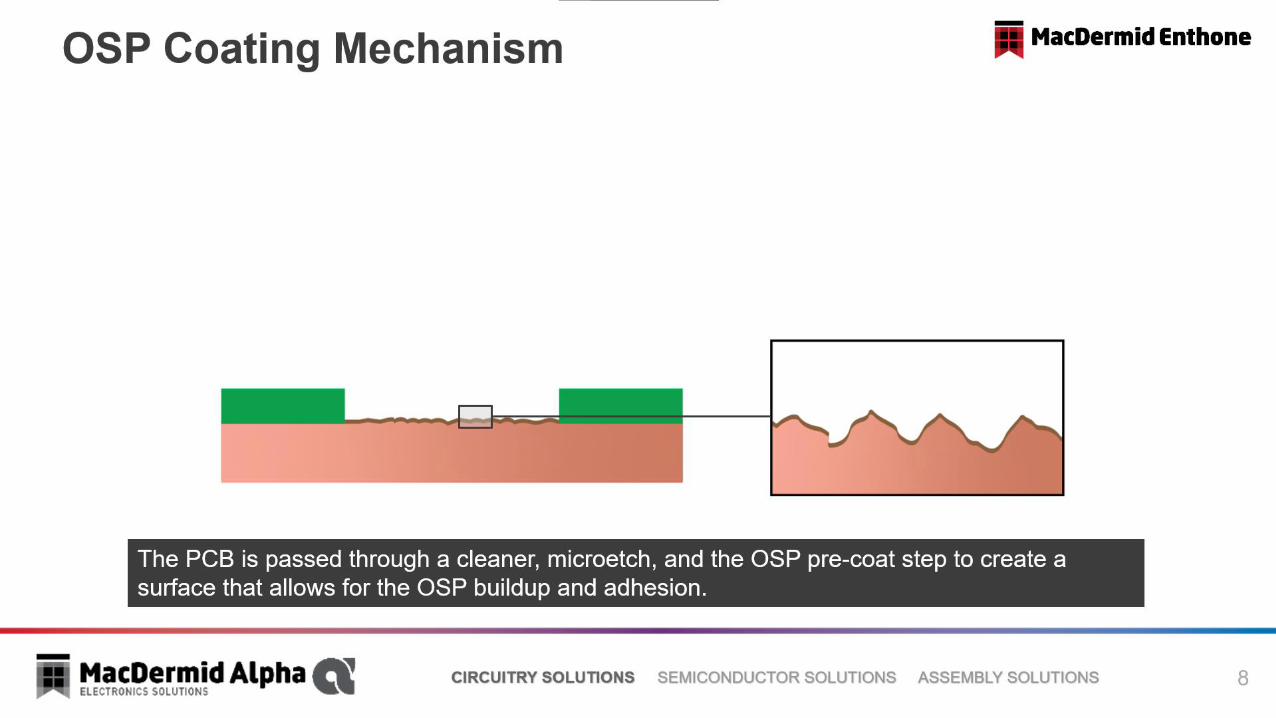
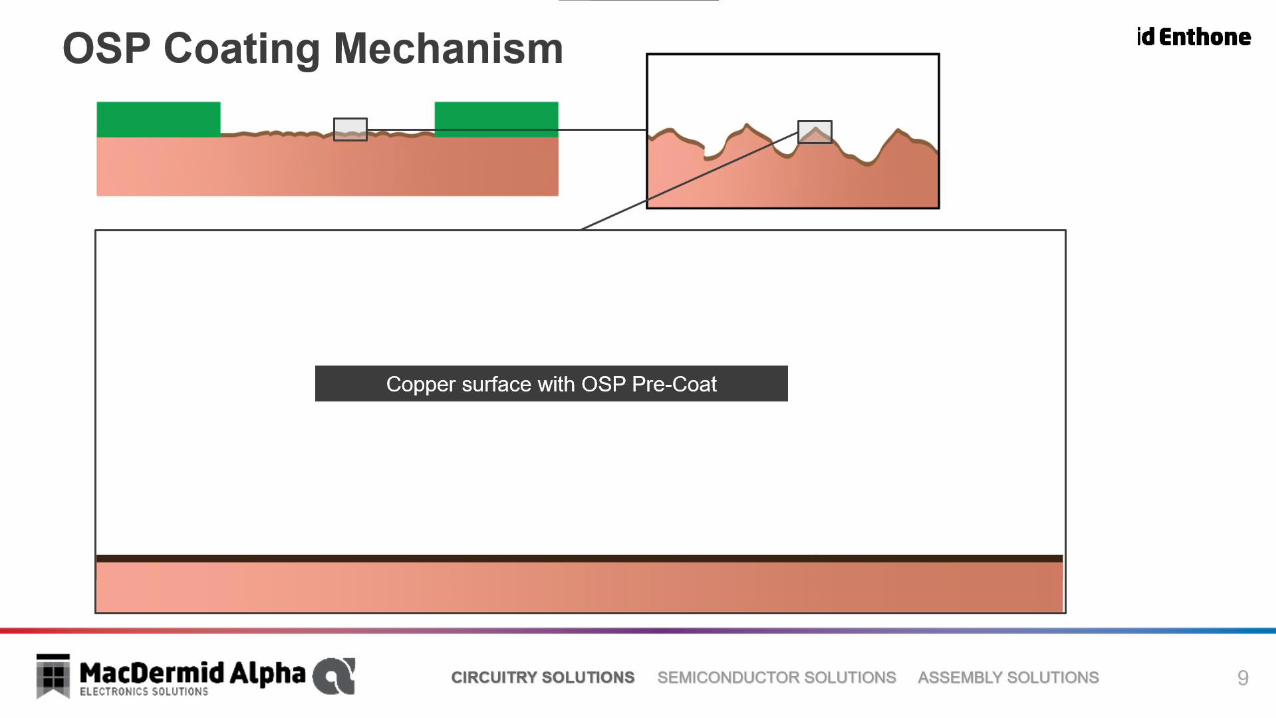
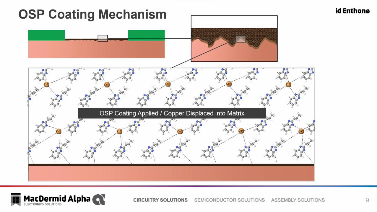
OSP Process Overview
Standard Pretreatment Objectives
▪ The cleaner removes fingerprints and
other contaminants.
▪ Cleaners may be acidic or alkaline.
Alkaline cleaners are required to remove
soldermask residues.
▪ The microetch will provide a micro-
roughened surface, that is relatively
oxide free.
Process Sequence
cleaner microetch precoatOSP
CoatingDryrinse rinse rinse rinse
Precoat
▪ The Precoat deposits a
thin, organic film, which
is covalently bonded to
the copper surface.
▪ This organic film
increases the useful life
of the OSP bath and
allows an easy method
to adjust the OSP film
thickness.
OSP Coating and Dry
▪ The OSP bath builds the coating
thickness to the desired level.
▪ An immersion time of 1 minute will
produce a coating thickness of 0.35
um.
▪ Acidity, temperature and Azole
concentration are key process drivers.
▪ The panels must be completely dry
before stacking
Total Cycle Time ~ 15 minutes
8CIRCUITRY SOLUTIONS SEMICONDUCTOR SOLUTIONS ASSEMBLY SOLUTIONS
9CIRCUITRY SOLUTIONS SEMICONDUCTOR SOLUTIONS ASSEMBLY SOLUTIONS
10CIRCUITRY SOLUTIONS SEMICONDUCTOR SOLUTIONS ASSEMBLY SOLUTIONS
11CIRCUITRY SOLUTIONS SEMICONDUCTOR SOLUTIONS ASSEMBLY SOLUTIONS
12CIRCUITRY SOLUTIONS SEMICONDUCTOR SOLUTIONS ASSEMBLY SOLUTIONS
13CIRCUITRY SOLUTIONS SEMICONDUCTOR SOLUTIONS ASSEMBLY SOLUTIONS

14CIRCUITRY SOLUTIONS SEMICONDUCTOR SOLUTIONS ASSEMBLY SOLUTIONS

15CIRCUITRY SOLUTIONS SEMICONDUCTOR SOLUTIONS ASSEMBLY SOLUTIONS
16CIRCUITRY SOLUTIONS SEMICONDUCTOR SOLUTIONS ASSEMBLY SOLUTIONS

17CIRCUITRY SOLUTIONS SEMICONDUCTOR SOLUTIONS ASSEMBLY SOLUTIONS

18CIRCUITRY SOLUTIONS SEMICONDUCTOR SOLUTIONS ASSEMBLY SOLUTIONS

19CIRCUITRY SOLUTIONS SEMICONDUCTOR SOLUTIONS ASSEMBLY SOLUTIONS
Immersion Silver Overview

20CIRCUITRY SOLUTIONS SEMICONDUCTOR SOLUTIONS ASSEMBLY SOLUTIONS
Immersion Silver
Overview:
▪ Lower cost than ENIG, ENEPIG, and Immersion tin
▪ Noteworthy in its Simplicity and Productivity
• Simple immersion coating reaction
• Time to deposit coating: ≈ 1 minute
▪ Best durability to multiple reflows
• No intermetallic formed with copper and silver
• Minimal surface oxidation
• No thermal breakdown of silver
▪ Electrical contact performance
▪ Excellent high frequency performance
21CIRCUITRY SOLUTIONS SEMICONDUCTOR SOLUTIONS ASSEMBLY SOLUTIONS
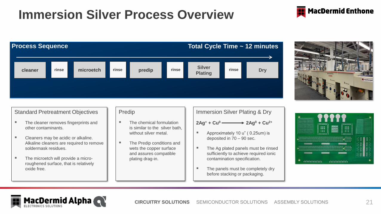
Immersion Silver Process Overview
Standard Pretreatment Objectives
▪ The cleaner removes fingerprints and
other contaminants.
▪ Cleaners may be acidic or alkaline.
Alkaline cleaners are required to remove
soldermask residues.
▪ The microetch will provide a micro-
roughened surface, that is relatively
oxide free.
Process Sequence
cleaner microetch predipSilver
PlatingDryrinse rinse rinse rinse
Predip
▪ The chemical formulation
is similar to the silver bath,
without silver metal.
▪ The Predip conditions and
wets the copper surface
and assures compatible
plating drag-in.
Immersion Silver Plating & Dry
2Ag+ + Cu0 2Ag0 + Cu2+
▪ Approximately 10 u” ( 0.25um) is
deposited in 70 – 90 sec.
▪ The Ag plated panels must be rinsed
sufficiently to achieve required ionic
contamination specification.
▪ The panels must be completely dry
before stacking or packaging.
Total Cycle Time ~ 12 minutes

22CIRCUITRY SOLUTIONS SEMICONDUCTOR SOLUTIONS ASSEMBLY SOLUTIONS
Consistent Solderability through 4+ high temperature reflows
▪ Unlike most PCB surface finishes, silver is unaffected by multiple heat exposures
• Minimal surface oxidation
• No intermetallic formation with copper substrate
Minimal change in silver
finish appearance after
assembly exposures
as coated 2x 4x
23CIRCUITRY SOLUTIONS SEMICONDUCTOR SOLUTIONS ASSEMBLY SOLUTIONS
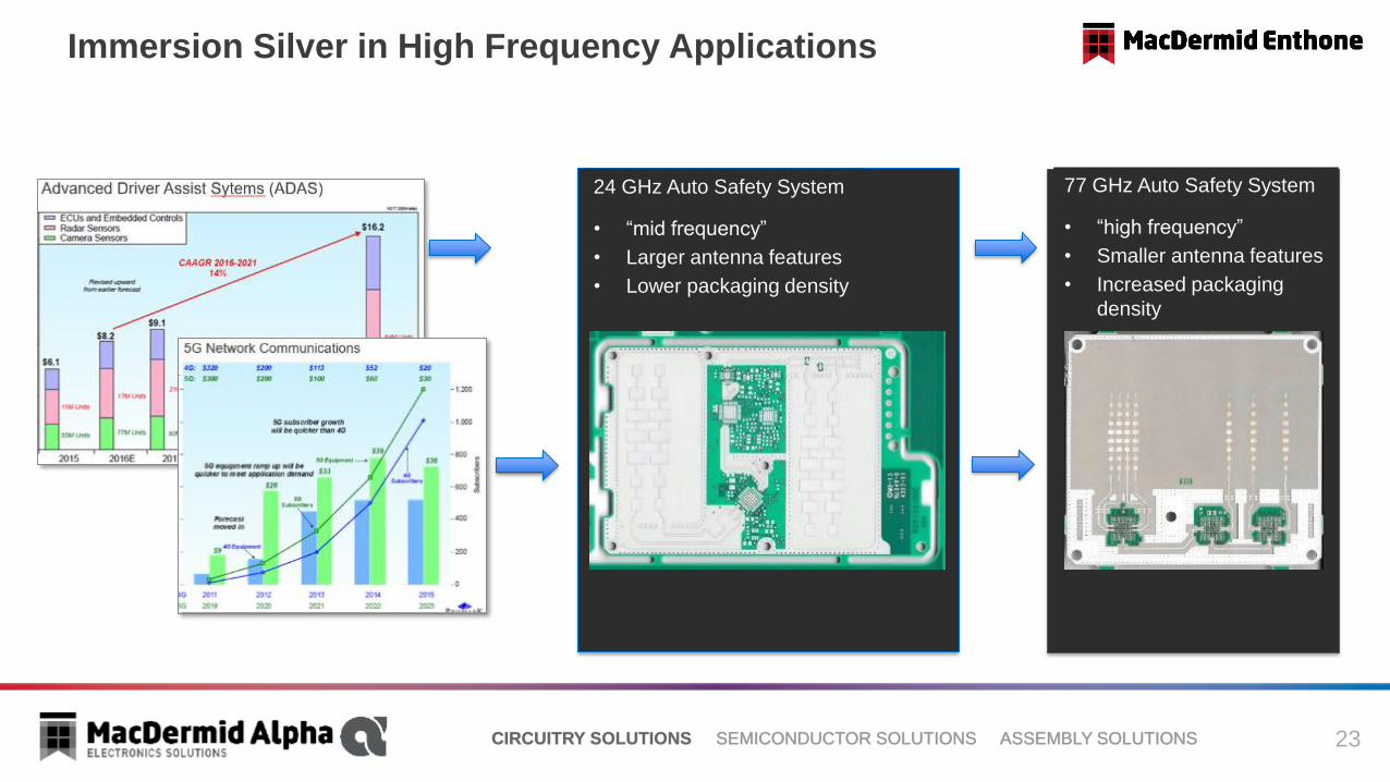
Immersion Silver in High Frequency Applications
24 GHz Auto Safety System
• “mid frequency”
• Larger antenna features
• Lower packaging density
77 GHz Auto Safety System
• “high frequency”
• Smaller antenna features
• Increased packaging
density
24CIRCUITRY SOLUTIONS SEMICONDUCTOR SOLUTIONS ASSEMBLY SOLUTIONS
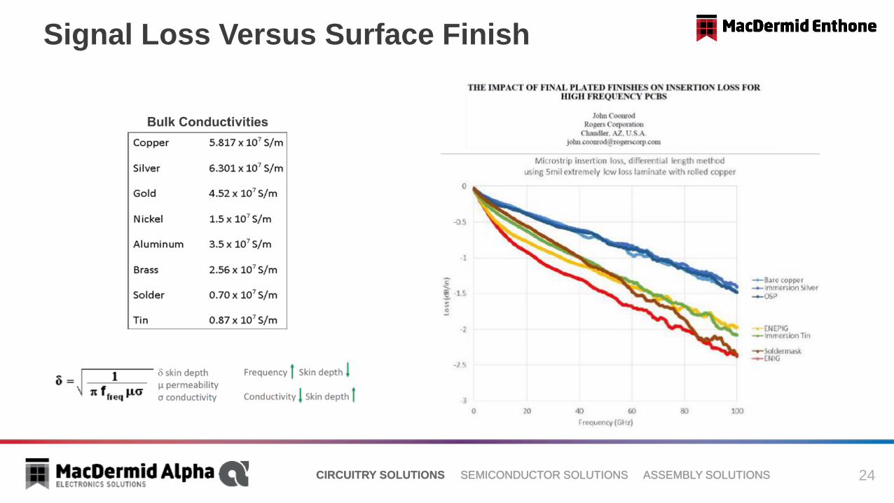
Signal Loss Versus Surface Finish

25
Immersion Silver – Tarnish Mitigation
Immersion silver without
tarnish inhibitorImmersion silver with
tarnish inhibitor
no reflow
preconditioning
after 1
assembly
exposure
after 2
assembly
exposures
no reflow
preconditioning
after 1
assembly
exposure
after 2
assembly
exposures
26CIRCUITRY SOLUTIONS SEMICONDUCTOR SOLUTIONS ASSEMBLY SOLUTIONS
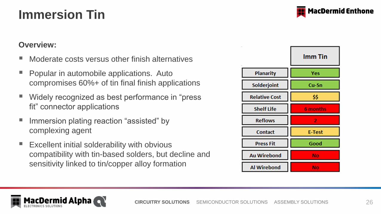
Immersion Tin
Overview:
▪ Moderate costs versus other finish alternatives
▪ Popular in automobile applications. Auto
compromises 60%+ of tin final finish applications
▪ Widely recognized as best performance in “press
fit” connector applications
▪ Immersion plating reaction “assisted” by
complexing agent
▪ Excellent initial solderability with obvious
compatibility with tin-based solders, but decline and
sensitivity linked to tin/copper alloy formation
27CIRCUITRY SOLUTIONS SEMICONDUCTOR SOLUTIONS ASSEMBLY SOLUTIONS
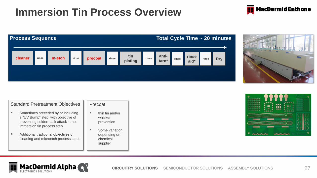
Immersion Tin Process Overview
Standard Pretreatment Objectives
▪ Sometimes preceded by or including
a “UV Bump” step, with objective of
preventing soldermask attack in hot
immersion tin process step
▪ Additional traditional objectives of
cleaning and microetch process steps
Process Sequence
cleaner Dryrinse
Precoat
▪ thin tin and/or
whisker
prevention
▪ Some variation
depending on
chemical
supplier
Total Cycle Time ~ 20 minutes
m-etch rinse rinseprecoattin
plating
anti-
tarn*rinse rinse
rinse
aid*rinse
28CIRCUITRY SOLUTIONS SEMICONDUCTOR SOLUTIONS ASSEMBLY SOLUTIONS
Immersion Tin Process Overview
Standard Pretreatment Objectives
▪ Sometimes preceded by or including
a “UV Bump” step, with objective of
preventing soldermask attack in hot
immersion tin process step
▪ Additional traditional objectives of
cleaning and microetch process steps
Process Sequence
cleaner Dryrinse
Precoat
▪ thin tin and/or
whisker
prevention
▪ Some variation
depending on
chemical
supplier
Tin Plating, Optional Post-treatments, and Dry
2Cu + Sn2+ Sn + 2Cu+ .
▪ Plating aided by complexing agent
▪ * Optional anti-tarn inhibits subsequent coating
oxidation
▪ * Optional rinse aid lowers “ionic contamination” of
board surface
Total Cycle Time ~ 20 minutes
m-etch rinse rinseprecoattin
plating
anti-
tarn*rinse rinse
rinse
aid*rinse
29CIRCUITRY SOLUTIONS SEMICONDUCTOR SOLUTIONS ASSEMBLY SOLUTIONS
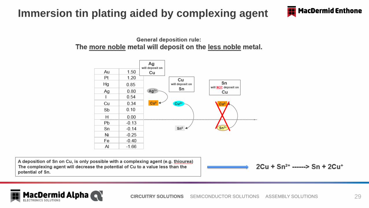
Immersion tin plating aided by complexing agent
30CIRCUITRY SOLUTIONS SEMICONDUCTOR SOLUTIONS ASSEMBLY SOLUTIONS
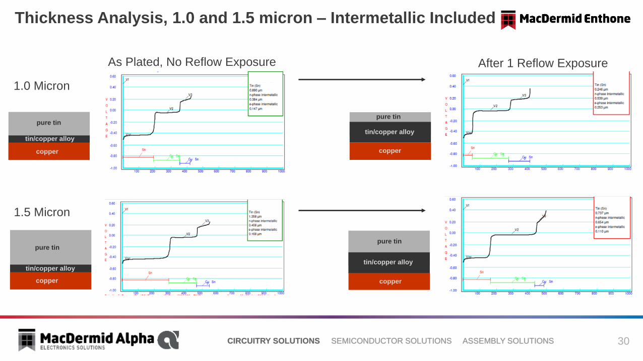
Thickness Analysis, 1.0 and 1.5 micron – Intermetallic Included
1.0 Micron
1.5 Micron
As Plated, No Reflow Exposure After 1 Reflow Exposure
copper
tin/copper alloy
pure tin
copper
tin/copper alloy
pure tin
copper
tin/copper alloy
pure tin
copper
tin/copper alloy
pure tin
31CIRCUITRY SOLUTIONS SEMICONDUCTOR SOLUTIONS ASSEMBLY SOLUTIONS
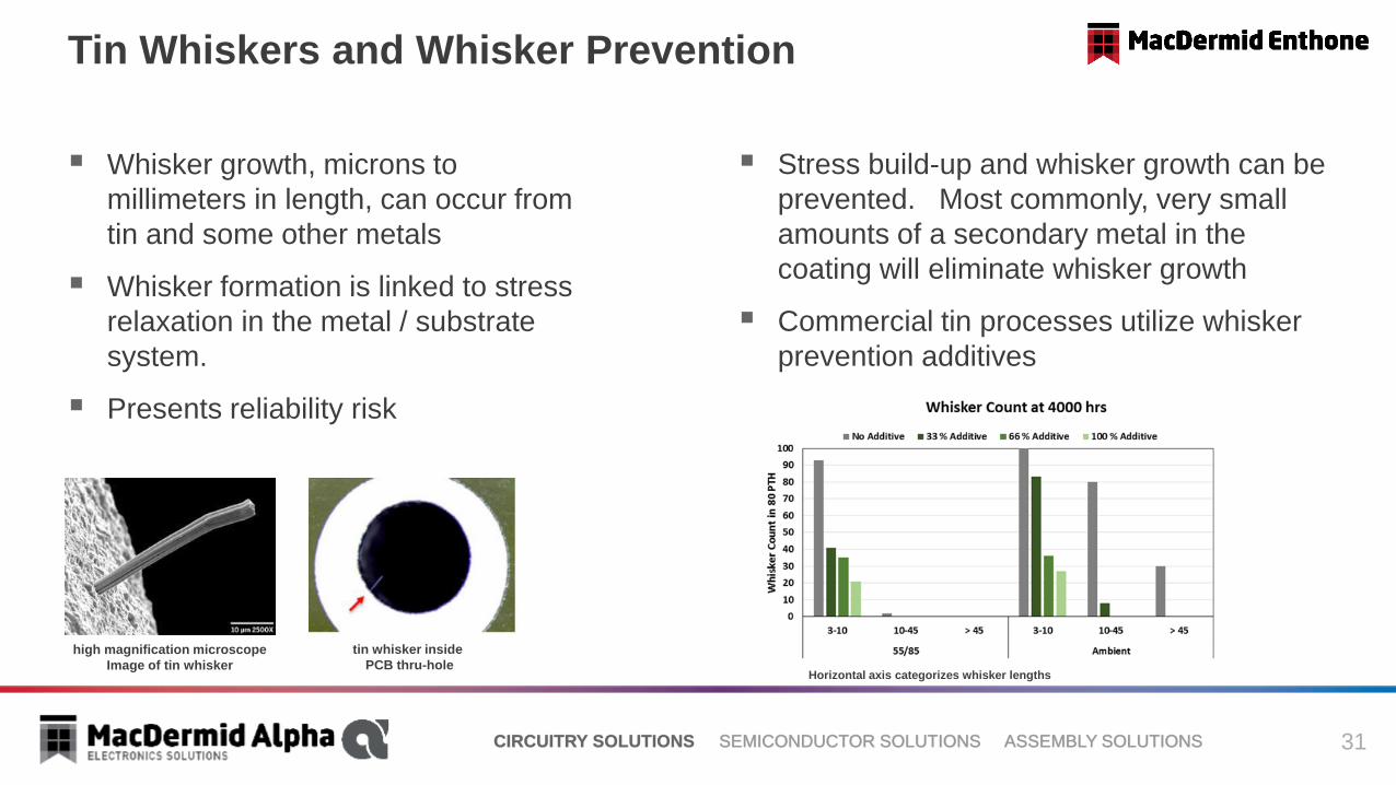
Tin Whiskers and Whisker Prevention
▪ Whisker growth, microns to
millimeters in length, can occur from
tin and some other metals
▪ Whisker formation is linked to stress
relaxation in the metal / substrate
system.
▪ Presents reliability risk
high magnification microscope
Image of tin whisker
tin whisker inside
PCB thru-hole
▪ Stress build-up and whisker growth can be
prevented. Most commonly, very small
amounts of a secondary metal in the
coating will eliminate whisker growth
▪ Commercial tin processes utilize whisker
prevention additives
Horizontal axis categorizes whisker lengths
32CIRCUITRY SOLUTIONS SEMICONDUCTOR SOLUTIONS ASSEMBLY SOLUTIONS
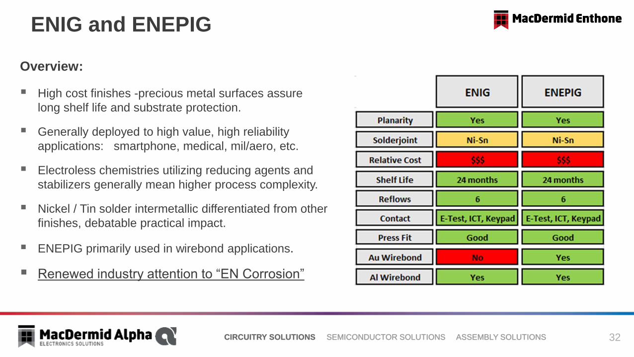
ENIG and ENEPIG
Overview:
▪ High cost finishes -precious metal surfaces assure
long shelf life and substrate protection.
▪ Generally deployed to high value, high reliability
applications: smartphone, medical, mil/aero, etc.
▪ Electroless chemistries utilizing reducing agents and
stabilizers generally mean higher process complexity.
▪ Nickel / Tin solder intermetallic differentiated from other
finishes, debatable practical impact.
▪ ENEPIG primarily used in wirebond applications.
▪ Renewed industry attention to “EN Corrosion”
33CIRCUITRY SOLUTIONS SEMICONDUCTOR SOLUTIONS ASSEMBLY SOLUTIONS
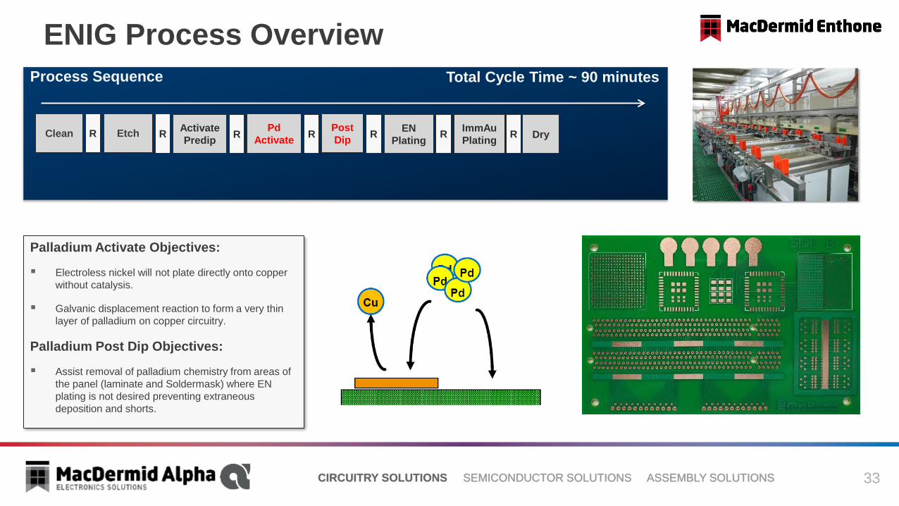
ENIG Process Overview
Palladium Activate Objectives:
▪ Electroless nickel will not plate directly onto copper
without catalysis.
▪ Galvanic displacement reaction to form a very thin
layer of palladium on copper circuitry.
Palladium Post Dip Objectives:
▪ Assist removal of palladium chemistry from areas of
the panel (laminate and Soldermask) where EN
plating is not desired preventing extraneous
deposition and shorts.
Process Sequence
Clean Dry
Total Cycle Time ~ 90 minutes
Pd
ActivateImmAu
PlatingEtch
Activate
PredipR
Post
DipR R R R
EN
PlatingR R
34CIRCUITRY SOLUTIONS SEMICONDUCTOR SOLUTIONS ASSEMBLY SOLUTIONS
ENIG Process Overview
Electroless Nickel Objectives:
▪ Deposition of a nickel – phosphorous alloy.
▪ Providing a barrier layer to copper migration through
to solderable surface.
▪ Provide a surface suitable for immersion gold
deposition that will allow soldering.
NaH2PO2 H2PO32-
H2O
[O] Ni
P
Copper Pad
Process Sequence
Clean Dry
Total Cycle Time ~ 90 minutes
Pd
ActivateImmAu
PlatingEtch
Activate
PredipR
Post
DipR R R R
EN
PlatingR R

35CIRCUITRY SOLUTIONS SEMICONDUCTOR SOLUTIONS ASSEMBLY SOLUTIONS
ENIG Process Overview
Immersion Gold Objectives:
▪ Deposition of a thin layer of pure gold
▪ Prevents oxidation of the electroless nickel
surface and preserves solderability.
▪ Gold is a noble metal and unreactive with
the environment thus providing long shelf
life and consistent soldering performance
with increasing assembly operations.
Ni 2+
Au +
e-
e-
Electroless Nickel Deposit
Copper Pad
Process Sequence
Clean Dry
Total Cycle Time ~ 90 minutes
Pd
ActivateImmAu
PlatingEtch
Activate
PredipR
Post
DipR R R R
EN
PlatingR R

36CIRCUITRY SOLUTIONS SEMICONDUCTOR SOLUTIONS ASSEMBLY SOLUTIONS
Current Industry ENIG Spec - IPC4552 Revision A
▪ IPC4552 A (August 2017) increases the quality bar for conforming ENIG deposits.
▪ All updates designed to minimize, control and evaluate ENIG corrosion.
▪ Changes to Gold Deposit Thickness Control and Measurement.
▪ Tighter gold thickness specification - lower minimum and introduction of new maximum gold thickness.
▪ Introduces XRF capability requirement and penalties for non-conforming instruments.
▪ New Requirement to Validate Electroless Nickel Phosphorous Content Control.
▪ EN %P dictates corrosion resistance and is not traditionally controlled by SPC.
▪ Adoption of new analytical techniques for compliance.
▪ New Requirement to Introduce Electroless Nickel Corrosion Analysis.
▪ X-Section evaluation for EN corrosion required as part of SPC.
▪ ENIG product is now rejectable if corrosion specification is not met.
37CIRCUITRY SOLUTIONS SEMICONDUCTOR SOLUTIONS ASSEMBLY SOLUTIONS
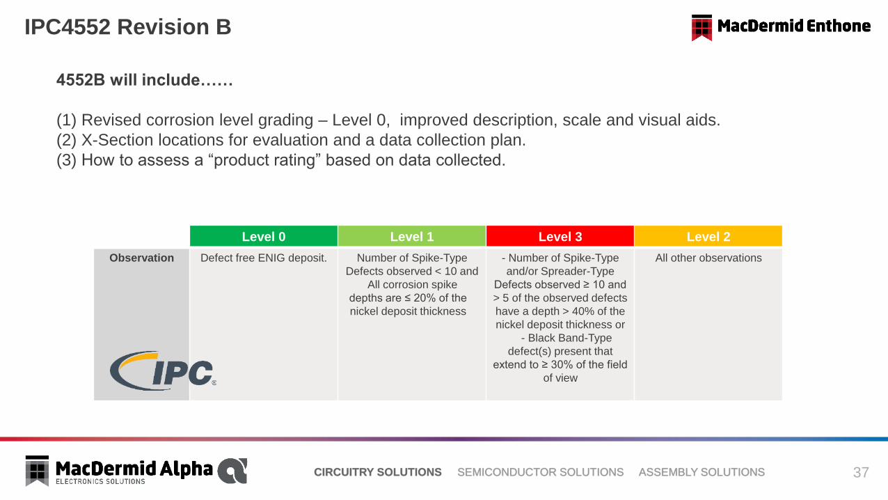
IPC4552 Revision B
4552B will include……
(1) Revised corrosion level grading – Level 0, improved description, scale and visual aids.
(2) X-Section locations for evaluation and a data collection plan.
(3) How to assess a “product rating” based on data collected.
Level 0 Level 1 Level 3 Level 2
Observation Defect free ENIG deposit. Number of Spike-Type
Defects observed < 10 and
All corrosion spike
depths are ≤ 20% of the
nickel deposit thickness
- Number of Spike-Type
and/or Spreader-Type
Defects observed ≥ 10 and
> 5 of the observed defects
have a depth > 40% of the
nickel deposit thickness or
- Black Band-Type
defect(s) present that
extend to ≥ 30% of the field
of view
All other observations

38CIRCUITRY SOLUTIONS SEMICONDUCTOR SOLUTIONS ASSEMBLY SOLUTIONS
Meeting ENIG IPC4552A Corrosion optimized ENIG control and chemistry selection
▪ All Immersion Gold deposition proceeds
via same chemical reaction.
▪ Good process control + good choice of
Nickel and Gold plating chemistry can
minimize corrosion
Anodic Reaction
Ni → Ni2+ + 2e-
Cathodic Reaction
2[Au(CN)2]- → 2Au+ + 4CN-
2Au+ + 2 e- → 2 Au
Overall Reaction
Ni + 2[Au(CN)2]- → 2Au + [Ni(CN)4]
2-
poor ENIG process control
39CIRCUITRY SOLUTIONS SEMICONDUCTOR SOLUTIONS ASSEMBLY SOLUTIONS
Gold Thickness Control - Highlights
Increased
corrosionIncreased
porosity
Targeted
Gold Control
Common
Control Spread
Ave Gold
Thickness
Reduction
Performance/Specification Concern Cost Concern
Targeted
Gold Control
Common
Control Spread
40CIRCUITRY SOLUTIONS SEMICONDUCTOR SOLUTIONS ASSEMBLY SOLUTIONS
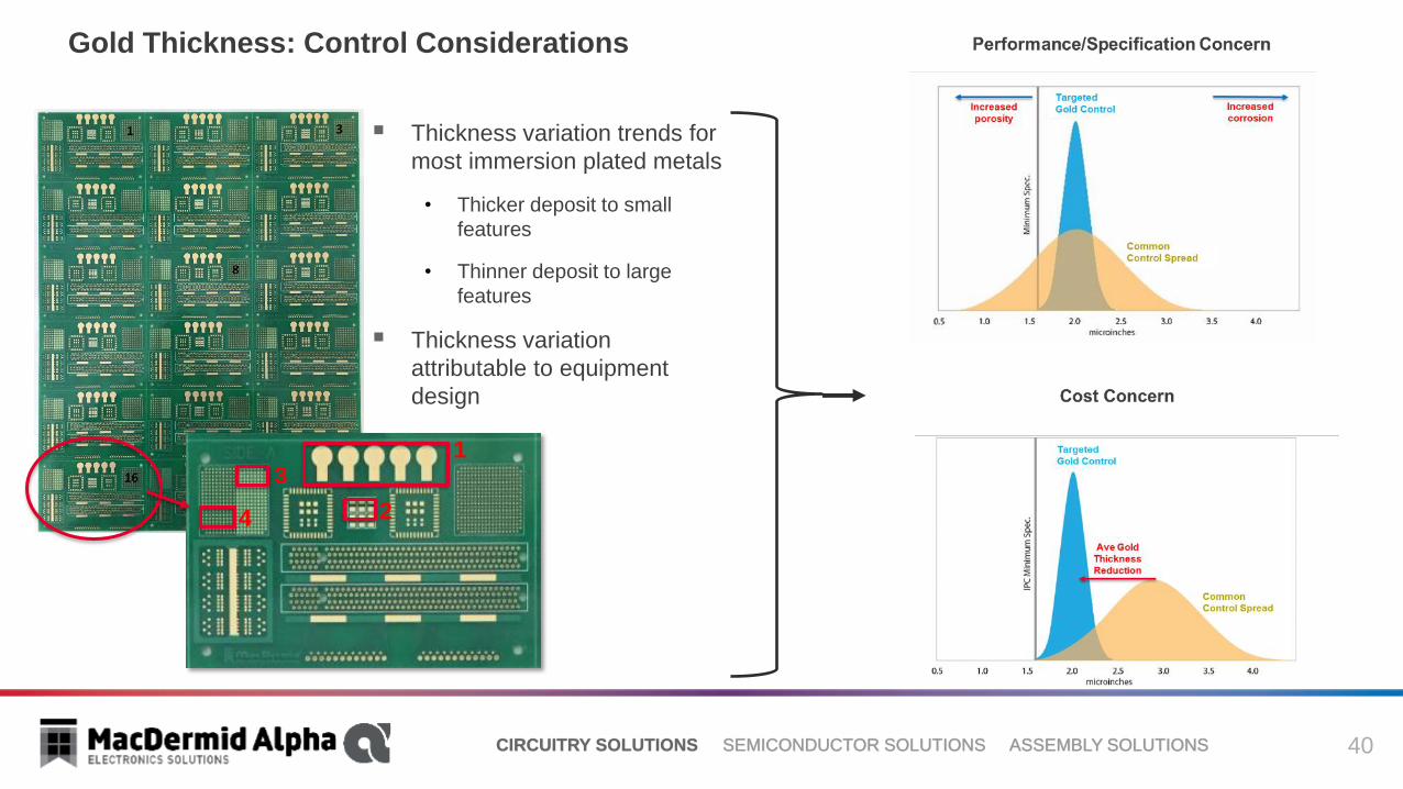
Gold Thickness: Control Considerations
▪ Thickness variation trends for
most immersion plated metals
• Thicker deposit to small
features
• Thinner deposit to large
features
▪ Thickness variation
attributable to equipment
design
1
24
3
41CIRCUITRY SOLUTIONS SEMICONDUCTOR SOLUTIONS ASSEMBLY SOLUTIONS
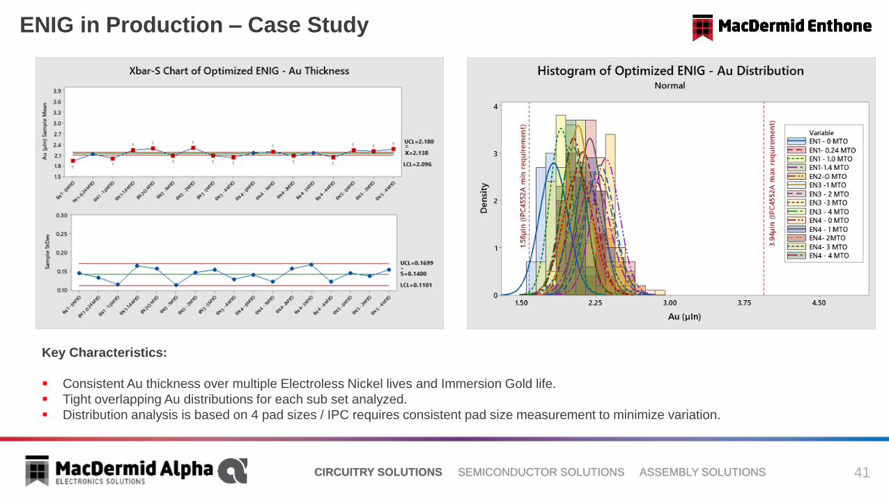
ENIG in Production – Case Study
Key Characteristics:
▪ Consistent Au thickness over multiple Electroless Nickel lives and Immersion Gold life.
▪ Tight overlapping Au distributions for each sub set analyzed.
▪ Distribution analysis is based on 4 pad sizes / IPC requires consistent pad size measurement to minimize variation.

42CIRCUITRY SOLUTIONS SEMICONDUCTOR SOLUTIONS ASSEMBLY SOLUTIONS
ENEPIG Process Overview
Electroless Palladium Objectives:
▪ Deposition of a palladium – phosphorous alloy onto
EN surface.
▪ Provide a surface suitable for gold deposition that
will allow gold wirebonding.
Process Sequence
Clean Dry
Total Cycle Time ~ 90 minutes
Pd
Activate
ImmAu
PlatingEtch
Activate
PredipR
Post
DipR R R R
EN
PlatingR
EPd
PlatingR
R
NaH2PO2 H2PO32-
H2O
[O] Pd
P
Electroless Nickel Deposit
Copper Pad
43CIRCUITRY SOLUTIONS SEMICONDUCTOR SOLUTIONS ASSEMBLY SOLUTIONS
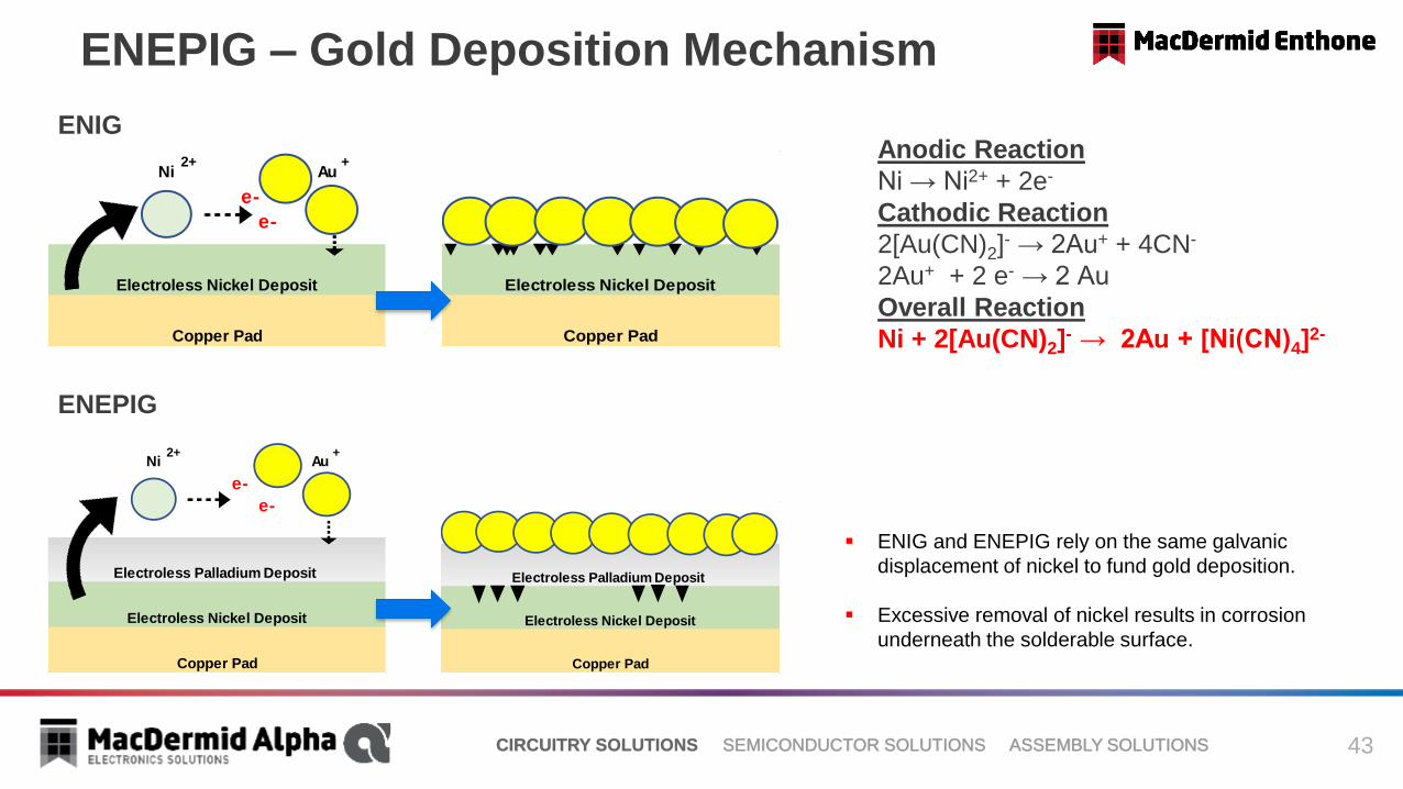
ENEPIG – Gold Deposition Mechanism
ENIG
ENEPIG
Anodic Reaction
Ni → Ni2+ + 2e-
Cathodic Reaction
2[Au(CN)2]- → 2Au+ + 4CN-
2Au+ + 2 e- → 2 Au
Overall Reaction
Ni + 2[Au(CN)2]- → 2Au + [Ni(CN)4]
2-
Ni 2+
Au +
e-
e-
Electroless Palladium Deposit
Electroless Nickel Deposit
Copper Pad
Ni 2+
Au +
e-
e-
Electroless Nickel Deposit
Copper Pad
Electroless Nickel Deposit
Copper Pad
▪ ENIG and ENEPIG rely on the same galvanic
displacement of nickel to fund gold deposition.
▪ Excessive removal of nickel results in corrosion
underneath the solderable surface.
Electroless Palladium Deposit
Electroless Nickel Deposit
Copper Pad

44CIRCUITRY SOLUTIONS SEMICONDUCTOR SOLUTIONS ASSEMBLY SOLUTIONS
Why Control ENIG Corrosion ?
▪ Too much and uncontrolled EN corrosion effects the normal IMC formation and can result in weak solderjoints !
Figure C: Ball-Shear Comparison of High Corrosion vs Low Corrosion ENIG
Laminate
1. Pad lift
2. Intermetallic(IMC)
3. Solder Joint
4. Bulk Solder
Figure A: Expected Ball-Shear Result Figure B: High Corrosion Ball-Shear Result
45CIRCUITRY SOLUTIONS SEMICONDUCTOR SOLUTIONS ASSEMBLY SOLUTIONS
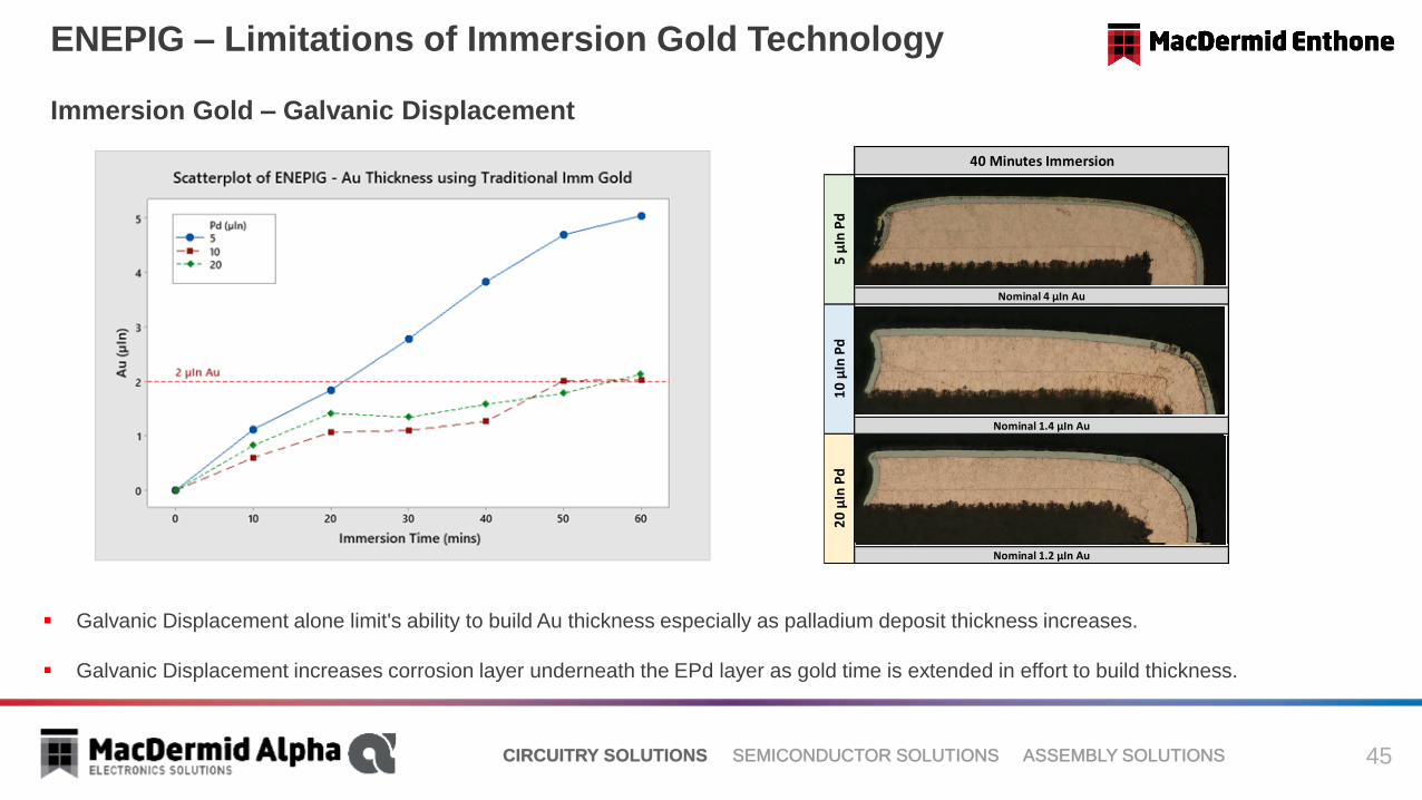
ENEPIG – Limitations of Immersion Gold Technology
Immersion Gold – Galvanic Displacement
▪ Galvanic Displacement alone limit's ability to build Au thickness especially as palladium deposit thickness increases.
▪ Galvanic Displacement increases corrosion layer underneath the EPd layer as gold time is extended in effort to build thickness.
Nominal 4 µIn Au
Nominal 1.4 µIn Au
40 Minutes Immersion
20
µIn
Pd
Nominal 1.2 µIn Au
5 µ
In P
d1
0 µ
In P
d
46CIRCUITRY SOLUTIONS SEMICONDUCTOR SOLUTIONS ASSEMBLY SOLUTIONS
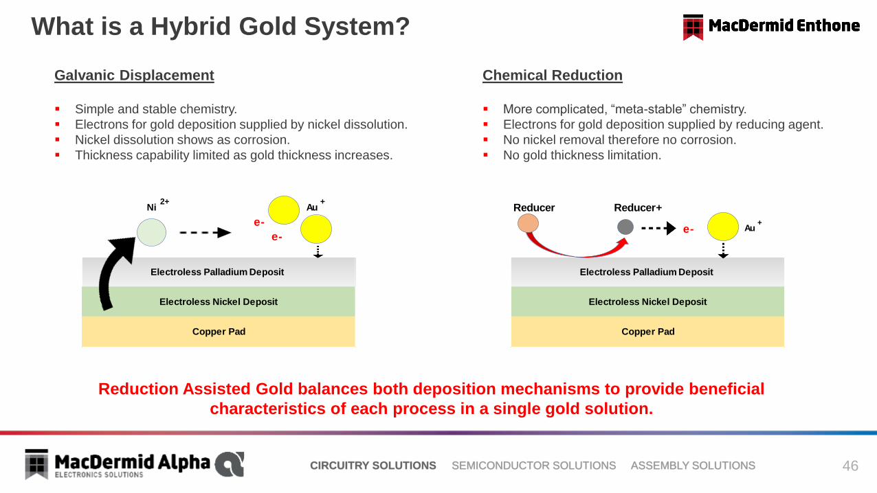
What is a Hybrid Gold System?
Reduction Assisted Gold balances both deposition mechanisms to provide beneficial
characteristics of each process in a single gold solution.
Galvanic Displacement
▪ Simple and stable chemistry.
▪ Electrons for gold deposition supplied by nickel dissolution.
▪ Nickel dissolution shows as corrosion.
▪ Thickness capability limited as gold thickness increases.
Chemical Reduction
▪ More complicated, “meta-stable” chemistry.
▪ Electrons for gold deposition supplied by reducing agent.
▪ No nickel removal therefore no corrosion.
▪ No gold thickness limitation.
Ni 2+
Au +
e-
e-
Copper Pad
Electroless Palladium Deposit
Electroless Nickel Deposit
Reducer Reducer+
Copper Pad
Electroless Palladium Deposit
Electroless Nickel Deposit
e- Au +
47CIRCUITRY SOLUTIONS SEMICONDUCTOR SOLUTIONS ASSEMBLY SOLUTIONS
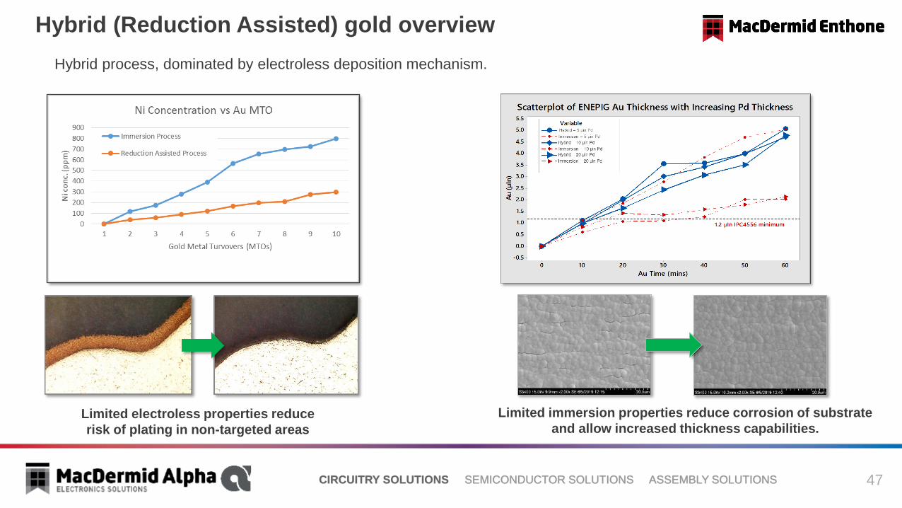
Hybrid (Reduction Assisted) gold overview
Hybrid process, dominated by electroless deposition mechanism.
Limited electroless properties reduce
risk of plating in non-targeted areas
Limited immersion properties reduce corrosion of substrate
and allow increased thickness capabilities.

48CIRCUITRY SOLUTIONS SEMICONDUCTOR SOLUTIONS ASSEMBLY SOLUTIONS
5 µIn Pd / 5 µIn Au
0%
10%
20%
30%
40%
50%
60%
70%
80%
90%
100%
10min
30min
50min
10min
30min
50min
10min
30min
50min
10min
30min
50min
10min
30min
50min
10min
30min
50min
10min
30min
50min
10min
30min
50min
10min
30min
50min
10min
30min
50min
10min
30min
50min
10min
30min
50min
10min
30min
50min
10min
30min
50min
10min
30min
50min
10min
30min
50min
10min
30min
50min
10min
30min
50min
10min
30min
50min
10min
30min
50min
10min
30min
50min
10min
30min
50min
10min
30min
50min
10min
30min
50min
10min
30min
50min
10min
30min
50min
10min
30min
50min
10min
30min
50min
5 µIn Pd 5 µIn Pd 10 µIn Pd 20 µIn Pd 5 µIn Pd 10 µIn Pd 20 µIn Pd 5 µIn Pd 10 µIn Pd 20 µIn Pd 5 µIn Pd 10 µIn Pd 20 µIn Pd 5 µIn Pd 10 µIn Pd 20 µIn Pd 5 µIn Pd 10 µIn Pd 20 µIn Pd 5 µIn Pd 10 µIn Pd 20 µIn Pd 5 µIn Pd 10 µIn Pd 20 µIn Pd 5 µIn Pd 10 µIn Pd 20 µIn Pd
Galv. Disp. 0 MTO 1 MTO 2 MTO 3 MTO 4 MTO 5 MTO 6 MTO 7 MTO 8 MTO
Immersion Gold ENEPIG - Corrosion Summary Level 0 Level 1 Level 2 Level 3
• Bar chart titleLevel 0 No observable corrosion
Level 1 less than 10 spikes, < 20% EN thickness
Level 2 all other observations
Level 3 more than 10 spikes, >40% EN thickness
5 µIn Pd / 5 µIn Au
5 µIn Pd / 5 µIn Au
ENEPIG Corrosion Summary:
▪ Galvanic displacement reaction requires more nickel dissolution to deposit more gold.
▪ Controlling nickel dissolution uniformity becomes more difficult with extended immersion gold time and thickness.
▪ ENEPIG corrosion increases significantly with extended immersion gold time and thickness.
ENEPIG – Immersion Gold System Corrosion Statistics

49CIRCUITRY SOLUTIONS SEMICONDUCTOR SOLUTIONS ASSEMBLY SOLUTIONS
ENEPIG – Hybrid Gold Corrosion Statistics
ENEPIG Corrosion Summary:
▪ Near zero corrosion performance observed over 0 – 8 MTO.
▪ No increase in corrosion could be correlated to increasing gold thickness.5 µIn Pd / 5 µIn Au
50CIRCUITRY SOLUTIONS SEMICONDUCTOR SOLUTIONS ASSEMBLY SOLUTIONS
John Swanson, Director of Final Finishes
Thank you for your attention….


![Temperature Effects in Automotive-Grade High Speed ... · the PCB manufacturer, the PCB substrate has an εrof approximately 3.6 and a loss tangentof 0.0117 [6]. In this paper we](https://static.fdocuments.net/doc/165x107/5e82b1b4f3308f35272e3bd8/temperature-effects-in-automotive-grade-high-speed-the-pcb-manufacturer-the.jpg)