PART NO. 12240636 Page 1 of 32 DELCO ELECTRONICS SYSTEMS … · part no. 12240636 page 2 of 32...
32
PART NO. 12240636 Page 1 of 32 DELCO ELECTRONICS SYSTEMS PART CATEGORY KEY PRODUCT CHARACTERISTICS PART CATEGORY ASSIGNMENT 2 SUBSTANCE OF CONCERN AND RECYCLE CONTENT PER DELPHI-A 10949001 SAFETY/COMPLIANCE FIT/FUNCTION See DE204.04 for Details TOTAL ON DRAWING 0 LAST NUMBER USED 0 THIS DRAWING IS THE PROPERTY OF DR. Mark Vincen DATE 18Nov03 DELPHI DELCO ELECTRONICS SYSTEMS NO RIGHTS ARE GRANTED TO USE THIS DRAWING CK. DATE FOR ANY PURPOSE OTHER THAN THE FURNISHING OF SERVICES AND SUPPLIES TO APPR Steve Netherton DATE 18NO03 DELPHI DELCO ELECTRONICS SYSTEMS APPR. DATE DISTRIBUTION FIRST USED: NAME: 15118439 MOD ASM - 6.5 INCH CHEV REFERENCE: PART NO: REV. Page 1 of 32 12228912 12240636 B
Transcript of PART NO. 12240636 Page 1 of 32 DELCO ELECTRONICS SYSTEMS … · part no. 12240636 page 2 of 32...

PART NO.
12240636 Page 1of 32 DELCO ELECTRONICS SYSTEMS
PART CATEGORY KEY PRODUCT CHARACTERISTICS
PART CATEGORYASSIGNMENT
2 SUBSTANCE OF CONCERN AND RECYCLE CONTENT PER DELPHI-A 10949001
SAFETY/COMPLIANCE
FIT/FUNCTION
See DE204.04 for Details TOTAL ON DRAWING 0LAST NUMBER USED 0
THIS DRAWING IS THE PROPERTY OF DR. Mark Vincen DATE 18Nov03
DELPHI DELCO ELECTRONICS SYSTEMS NO RIGHTS ARE GRANTED TO USE THIS DRAWING
CK. DATE
FOR ANY PURPOSE OTHER THAN THE FURNISHING OF SERVICES AND SUPPLIES TO APPR Steve Netherton DATE 18NO03
DELPHI DELCO ELECTRONICS SYSTEMS
APPR. DATE
DISTRIBUTION FIRST USED: NAME:15118439 MOD ASM - 6.5 INCH CHEV
REFERENCE: PART NO: REV. Page 1 of32
12228912 12240636 B

PART NO.
12240636 Page 2of 32 DELCO ELECTRONICS SYSTEMS
THIS DRAWING IS THE PROPERTY OF DELPHI DELCO ELECTRONICS SYSTEMS. NO RIGHTS ARE GRANTED TO USE THIS DRAWING FOR ANY
PURPOSE OTHER THAN THE FURNISHING OF SERVICES AND SUPPLIES TO DELPHI DELCO ELECTRONICS SYSTEMS
PART NO:
12240636REV.
BPage 2 of 32
TABLE OF CONTENTS
1. GENERAL OVERVIEW .............................................................................................................................................................3
1.1. MODULE SCOPE..........................................................................................................................................................................31.2. GENERAL SPECIFICATION............................................................................................................................................................31.3. TEMPERATUREOPERATIONCONDITIONS....................................................................................................................................41.4. FUNCTIONAL BLOCK DIAGRAM...................................................................................................................................................4
2. APPLICABLE DOCUMENTS....................................................................................................................................................5
2.1. APPLICABLE REFERENCE DOCUMENTS FOR PURCHASED DISPLAY MODULE.................................................................................5
3. ELECTRICAL REQUIREMENTS.............................................................................................................................................5
3.1. MINIMUM /MAXIMUM ELECTRICAL PARAMETERS(TOP= 25ºC +/-5ºC) .....................................................................................53.2. ELECTRICAL OPERATINGCONDITIONS........................................................................................................................................63.3. VIDEO I/O INTERFACE................................................................................................................................................................83.4. A/C SIGNAL TIMING REQUIREMENTS..........................................................................................................................................93.5. ANALOG SIGNAL TIMING DIAGRAM ..........................................................................................................................................103.6. SELECTABLE DISPLAY CONFIGURATIONINPUTS.......................................................................................................................123.7. VIEW MODESELECTIONFORMAT.............................................................................................................................................123.8 SELF-HEATING BACKLIGHT CHARACTERISTICS.........................................................................................................................133.9 THERMISTOR CHARACTERISTICS...............................................................................................................................................14
4. MECHANICAL SPECIFICATIONS........................................................................................................................................15
4.1. MODULE DIMENSIONEDOUTLINE DRAWING.............................................................................................................................154.2. MODULE MOUNTING GUIDELINES.............................................................................................................................................174.3. FACTORY IDENTIFICATION AND PRODUCTIONDATE CODING....................................................................................................18
5. OPTICAL CHARACTERISTICS.............................................................................................................................................19
5.1. OPTICAL PERFORMANCETABLE ...............................................................................................................................................195.2. EQUI-CONTRASTPLOT..............................................................................................................................................................205.3. DISPLAY PIXEL CONFIGURATION...............................................................................................................................................215.4. FLUID CLEARING POINT TEMPERATURE....................................................................................................................................215.5. DEFECTIVEPIXEL CRITERIA......................................................................................................................................................225.6 COSMETIC DEFECTS..................................................................................................................................................................235.7. POLARIZER DEFINITION.............................................................................................................................................................23
6. PRODUCT ASSURANCE PROVISIONS................................................................................................................................24
6.1. SCREENING...............................................................................................................................................................................246.2. ELECTRICAL AND OPTICAL TESTING.........................................................................................................................................246.3. QUALITY CONFORMANCEINSPECTION......................................................................................................................................24
7. QUALIFICATION TESTING...................................................................................................................................................25
7.1. QUALIFICATION TESTMETHODS...............................................................................................................................................257.2. QUALIFICATION TESTFLOW......................................................................................................................................................267.3 ENDPOINT REQUIREMENTS........................................................................................................................................................27
8. PACKAGING METHOD FOR SHIPMENT...........................................................................................................................29
8.1. PACKAGING DRAWING..............................................................................................................................................................29
9. APPLICATION NOTES............................................................................................................................................................31
9.1. PROTECTIVEFILM .....................................................................................................................................................................31

PART NO.
12240636 Page 3of 32 DELCO ELECTRONICS SYSTEMS
THIS DRAWING IS THE PROPERTY OF DELPHI DELCO ELECTRONICS SYSTEMS. NO RIGHTS ARE GRANTED TO USE THIS DRAWING FOR ANY
PURPOSE OTHER THAN THE FURNISHING OF SERVICES AND SUPPLIES TO DELPHI DELCO ELECTRONICS SYSTEMS
PART NO:
12240636REV.
BPage 3 of 32
9.2. LCD CLEANING ........................................................................................................................................................................319.3. MECHANICAL STRESS................................................................................................................................................................31
1. GENERAL OVERVIEW
1.1. Module Scope
This specification covers the detailed requirements for a full color TFT-LCD monitor. The monitor hasbeen engineered to operate within the vehicle passenger compartment under most environmental conditions.Details of the performance criteria are contained in subsequent sections of this document. Operation outside theindicated design parameters will result in a lose of performance and possible permanent damage. The part isESD sensitive and should be handled accordingly.
1.2. General Specification
Characteristic Item Specification Remark
Picture Size Diagonal 16.5 cm (6.5 inch)
Active Area 143.4 mm x 79.3 mm
Display Technology Full color a-Si TFT active matrix normally white
Display Modes Normal, full, cinema, wide(zoom) Formats
Number of Pixels 400(H) X RGB X 234(V) 1200(H) X 234(V)
Dot Pitch 0.1195(H) X 0.339(V) mm
Pixel Orientation RGB stripe
Optimum Viewing Angle 6 o’clock
Power DC +12.0 VDC (typ) for video
DC +8.0 - +18.0 VDC for backlight
Signal Composite video (NTSC and PAL) + Analog RGB (NTSC and PAL)
InputSignals
Control Bright, Color, Tint, PWMI, HRV, VRV,Video Modes,CLK,CLKC,
VSW, NTP
Backlight Cold Cathode Fluorescent Lamps with temp controlled boost function
Mercury content 3.8 mg TYP, 5.0 mg MAX
Brightness Typical 635cd/m2
Front Surface Treatment AG
Weight 290 grams
Dimensions 156.8(W) X 91.5(H) X 18.0(D) mm
Display Life To 50% initial brightness: 10K hrs minimum

PART NO.
12240636 Page 4of 32 DELCO ELECTRONICS SYSTEMS
THIS DRAWING IS THE PROPERTY OF DELPHI DELCO ELECTRONICS SYSTEMS. NO RIGHTS ARE GRANTED TO USE THIS DRAWING FOR ANY
PURPOSE OTHER THAN THE FURNISHING OF SERVICES AND SUPPLIES TO DELPHI DELCO ELECTRONICS SYSTEMS
PART NO:
12240636REV.
BPage 4 of 32
1.3. Temperature Operation ConditionsValueItem Symbol Conditions
Min. Max.
Unit
Operating Temperature Top Must meet specification requirements -30 70 °C
Storage Temperature Tstg Module Unpowered -40 85 °C
1.4. Functional Block Diagram
V. Mode 1-3
Power
ControlCircuit
Backlight
GND1
NTP
HRV, VRV
HSY, VSY
CLKC
VideoCircuit
VSW
VBS
RG B
RGB Sync
Bright
Color
Tint
VBL
GND2
PWMI
Gate
Driver
Source Driver
AMLCD
Backlight
VCC
CLK
THM Thermistor GND1

PART NO.
12240636 Page 5of 32 DELCO ELECTRONICS SYSTEMS
THIS DRAWING IS THE PROPERTY OF DELPHI DELCO ELECTRONICS SYSTEMS. NO RIGHTS ARE GRANTED TO USE THIS DRAWING FOR ANY
PURPOSE OTHER THAN THE FURNISHING OF SERVICES AND SUPPLIES TO DELPHI DELCO ELECTRONICS SYSTEMS
PART NO:
12240636REV.
BPage 5 of 32
2. APPLICABLE DOCUMENTS
2.1. Applicable reference documents for purchased display module
In case of conflict the following documentation order of precedence shall apply.
A. Purchase order
B. This part drawing
C. Other reference documents such as the supplier specification.
3. ELECTRICAL REQUIREMENTS
The following signal characteristics are required in order to guarantee the reliability and performance ofthe display module in the application. It is not required that every module be tested for all signal characteristicsthough all modules must perform the same within the specification limits when installed in the vehicle application.
3.1. Minimum/Maximum Electrical Parameters (Top = 25ºC +/-5ºC)MAXIMUM
ABSOLUTE RATINGS- Note 1
ITEMS SYMBOL CONDITIONS MIN. MAX. UNIT Remarks
SUPPLYPOWER
for Video Circuit VCC VSS-1.0 +14.0 V Note 1
ICC 1.0 A
for B/L Inverter VBL VSS-1.0 +24.0 V
IBL 2.0 A
VOLTAGE VSS = 0V
Notes 1,2
INPUTSIGNAL
CompositeVideo
VIDEO -- 1.5 Vp-p Note 1
Analog RGB R, G, B VCC = 8.0V -- 1.5 Vp-p
RGB CompositeSync.
SYNC VBL = 8.0V75Ω
-- 1.5 Vp-p
Color, TintBright, PWMI
COLOR, TINT, BRIGHTPWMI VSS = 0V
VDD = 5.0V
VSS-0.2 VDD+0.4 V Note 1
Signal Switch SSW, VSW MODE 1~3L/R, U/D, N/P
VCC = 8.0VVBL = 8.0V
VSS-0.2 VDD+0.4 V
Note 1: Do not exceed the maximum rating values, otherwise the module may be damaged.
Note 2. +24V time duration is two (2) minutes

PART NO.
12240636 Page 6of 32 DELCO ELECTRONICS SYSTEMS
THIS DRAWING IS THE PROPERTY OF DELPHI DELCO ELECTRONICS SYSTEMS. NO RIGHTS ARE GRANTED TO USE THIS DRAWING FOR ANY
PURPOSE OTHER THAN THE FURNISHING OF SERVICES AND SUPPLIES TO DELPHI DELCO ELECTRONICS SYSTEMS
PART NO:
12240636REV.
BPage 6 of 32
3.2. Electrical Operating Conditions
When operated within these limits, display uniformity shall be guaranteed by design. The specific intendedapplication will provide the necessary protection circuitry to guarantee the specified limits are not exceeded.
(Top = 25ºC +/- 5ºC, VSS= 0V, VDD= +5.0V)
SPECIFICATION (Note 1)
ITEMS SYMBOL CONDITIONS MIN. TYP. MAX. UNIT Remarks
for Video Circuit VCC 8.0 12.0 14.0 VSUPPLYPOWER ICC
VCC=12.0V
VBL=13.8V 160 200 mA
for B/L Inverter VBL 8.0 13.8 18.0 V
IBL 325 400 mA
for DisplayControl
VDD VSS --- VDD V
(Color, Bright, Tint)
VOLTAGE
CONTROL
VOLTAGEReference
VIDEO -- .714 -- Vp-p
Sync .272 .286 .300 Vp-p
INPUTSIGNAL
Composite Video
Chroma/burst .272 .286 .300 Vp-p
VOLTAGE Analog RGB R, G, B 75Ω -- 0.7 -- Vp-p
Composite sync. SYNC -- 1.0 -- Vp-p
Brightness BRT 0.0 2.8 5.0 V adjustable
Tint TINT 0.0 2.9 5.0 V adjustable
Color COLOR 0.0 2.1 5.0 V adjustable
B/L DimmerAdjust
PWMI 0.0 -- 5.0 V PWM
B/L Dimmer
Adjust
PWMI 145 150 155 Hz Base Freq
Signal Switch NTP,HRV,VRV,
MODS, MODW,MODN, CLKC,VSW
H Level4.0 -- VDD V
L Level VSS -- 1.0 V
Selectable
FIELD FREQUENCY fVDN NTSC 57.14 59.93 62.86 Hz
fHDN 15.0 15.73 16.50 kHz
fVDP PAL 48.64 50.0 56.20 Hz
fHDP 15.20 15.62 16.00 kHz

PART NO.
12240636 Page 7of 32 DELCO ELECTRONICS SYSTEMS
THIS DRAWING IS THE PROPERTY OF DELPHI DELCO ELECTRONICS SYSTEMS. NO RIGHTS ARE GRANTED TO USE THIS DRAWING FOR ANY
PURPOSE OTHER THAN THE FURNISHING OF SERVICES AND SUPPLIES TO DELPHI DELCO ELECTRONICS SYSTEMS
PART NO:
12240636REV.
BPage 7 of 32
Note 1: The recommended operating conditions show the ranges in which the device can operate normally.
Operation beyond the limit of the recommended operation conditions is not assured, even though operating conditions are within the limit of the absolute maximum ratings.
Note 2. The BRT, COLOR, TINT inputs default to the factory setting when no signal is applied
Note 3. The PWMI (DIM) input is internally pulled up to VDD (5VDC). The CCFL backlight is at full intensity when PWM1 is at 5VDC (active high functionality)
Note 4: The module shall reset itself if the power supply input voltages VCC and VBL fall below minimum values and then are restored to normal values.
PART NO.
12240636 Page 8of 32 DELCO ELECTRONICS SYSTEMS
THIS DRAWING IS THE PROPERTY OF DELPHI DELCO ELECTRONICS SYSTEMS. NO RIGHTS ARE GRANTED TO USE THIS DRAWING FOR ANY
PURPOSE OTHER THAN THE FURNISHING OF SERVICES AND SUPPLIES TO DELPHI DELCO ELECTRONICS SYSTEMS
PART NO:
12240636REV.
BPage 8 of 32
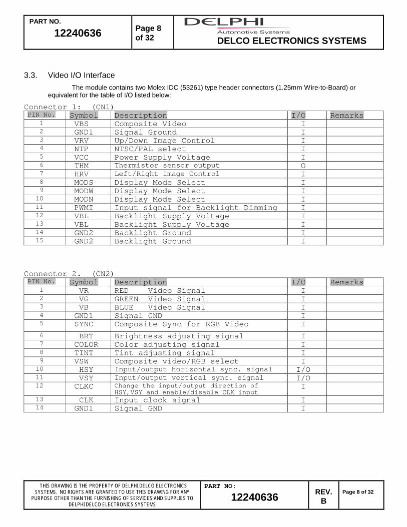
3.3. Video I/O Interface
The module contains two Molex IDC (53261) type header connectors (1.25mm Wire-to-Board) orequivalent for the table of I/O listed below:
Connector 1: (CN1)PIN No. Symbol Description I/O Remarks
1 VBS Composite Video I2 GND1 Signal Ground I3 VRV Up/Down Image Control I4 NTP NTSC/PAL select I5 VCC Power Supply Voltage I6 THM Thermistor sensor output O7 HRV Left/Right Image Control I8 MODS Display Mode Select I9 MODW Display Mode Select I
10 MODN Display Mode Select I11 PWMI Input signal for Backlight Dimming I12 VBL Backlight Supply Voltage I13 VBL Backlight Supply Voltage I14 GND2 Backlight Ground I15 GND2 Backlight Ground I
Connector 2. (CN2)PIN No. Symbol Description I/O Remarks
1 VR RED Video Signal I2 VG GREEN Video Signal I3 VB BLUE Video Signal I4 GND1 Signal GND I5 SYNC Composite Sync for RGB Video I
6 BRT Brightness adjusting signal I7 COLOR Color adjusting signal I8 TINT Tint adjusting signal I9 VSW Composite video/RGB select I
10 HSY Input/output horizontal sync. signal I/O11 VSY Input/output vertical sync. signal I/O12 CLKC Change the input/output direction of
HSY,VSY and enable/disable CLK inputI
13 CLK Input clock signal I14 GND1 Signal GND I

PART NO.
12240636 Page 9of 32 DELCO ELECTRONICS SYSTEMS
THIS DRAWING IS THE PROPERTY OF DELPHI DELCO ELECTRONICS SYSTEMS. NO RIGHTS ARE GRANTED TO USE THIS DRAWING FOR ANY
PURPOSE OTHER THAN THE FURNISHING OF SERVICES AND SUPPLIES TO DELPHI DELCO ELECTRONICS SYSTEMS
PART NO:
12240636REV.
BPage 9 of 32
3.4. A/C Signal Timing Requirements
Symbol Description Min. Typ. Max. UnitVertical sync pulse width(NTP=H) 15.6 16.7 17.8 mstW(V)
Vertical sync pulse width(NTP=L) 19.0 20.0 21.0 msVertical sync hold time (NTP=H) 181.8 190.7 199.6 ustH(V)
Vertical sync hold time (NTP=L) 187.5 192.1 196.7 usVertical sync set-up time(NTP=H) 15.4 16.5 17.6 mstSU(V)
Vertical sync set-up time(NTP=L) 18.8 19.8 20.8 msHorizontal sync pulse width(NTP=H) 60.6 63.6 66.6 ustW(H)
Horizontal sync pulse width(NTP=L) 62.5 64.0 65.5 ustH(H) Horizontal sync hold time 4.2 4.7 5.2 us
Horizontal sync set-up time(NTP=H) 55.4 58.9 62.4 ustSU(H)
Horizontal sync set-up time(NTP=L) 57.3 59.3 61.3 us

PART NO.
12240636 Page 10of 32 DELCO ELECTRONICS SYSTEMS
THIS DRAWING IS THE PROPERTY OF DELPHI DELCO ELECTRONICS SYSTEMS. NO RIGHTS ARE GRANTED TO USE THIS DRAWING FOR ANY
PURPOSE OTHER THAN THE FURNISHING OF SERVICES AND SUPPLIES TO DELPHI DELCO ELECTRONICS SYSTEMS
PART NO:
12240636REV.
BPage 10 of 32
3.5. Analog Signal Timing Diagram: (Composite Video)
10.75 us
1.96

PART NO.
12240636 Page 11of 32 DELCO ELECTRONICS SYSTEMS
THIS DRAWING IS THE PROPERTY OF DELPHI DELCO ELECTRONICS SYSTEMS. NO RIGHTS ARE GRANTED TO USE THIS DRAWING FOR ANY
PURPOSE OTHER THAN THE FURNISHING OF SERVICES AND SUPPLIES TO DELPHI DELCO ELECTRONICS SYSTEMS
PART NO:
12240636REV.
BPage 11 of 32
Analog Signal Timing Diagram: (RGB Video)
11.125us
1.96

PART NO.
12240636 Page 12of 32 DELCO ELECTRONICS SYSTEMS
THIS DRAWING IS THE PROPERTY OF DELPHI DELCO ELECTRONICS SYSTEMS. NO RIGHTS ARE GRANTED TO USE THIS DRAWING FOR ANY
PURPOSE OTHER THAN THE FURNISHING OF SERVICES AND SUPPLIES TO DELPHI DELCO ELECTRONICS SYSTEMS
PART NO:
12240636REV.
BPage 12 of 32
3.6. Selectable Display Configuration Inputs
The following signal inputs are selectable and control the video format and performance of the display as part ofthe overall video system. (H=VDD [5VDC], L=GND1)
Symbol Function Input LevelMODS Display mode select See Section 3.7
MODW Display mode select See Section 3.7
MODN Display mode select See Section 3.7
Internal Clock * HCLKC I/O direction of CLK,HSY,VSYExternal Clock LNTSC format * HNTP NTSC/PAL selectionPAL format LNormal * HVRV Up/Down Image ControlInvert image LNormal * HHRV Left/Right Image ControlShift image left to right LComposite video * HVSW Analog RGB/ Composite Video selectionAnalog RGB video L
Note: All control inputs have internal pull-up resistors to the default state* indicates default state
Display mode control defaults to FULL Mode
3.7. View Mode Selection Format
The five possible view modes are vehicle occupant selectable using a menu system and an input device.

PART NO.
12240636 Page 13of 32 DELCO ELECTRONICS SYSTEMS
THIS DRAWING IS THE PROPERTY OF DELPHI DELCO ELECTRONICS SYSTEMS. NO RIGHTS ARE GRANTED TO USE THIS DRAWING FOR ANY
PURPOSE OTHER THAN THE FURNISHING OF SERVICES AND SUPPLIES TO DELPHI DELCO ELECTRONICS SYSTEMS
PART NO:
12240636REV.
BPage 13 of 32
Description of Display Modes:
1. Full Mode 16:9: The picture is displayed with uniform enlargement in the horizontal directionand the horizontal retrace line on the input signal cannot be seen. If the video samplingfrequency of the image is fixed and a 4:3 video signal is displayed, the picture will be oblong.
2. Wide Mode: A 4:3 video signal is displayed with less feeling of incongruity than in the fullscreen mode. Since the video horizontal sampling frequency is modulated in the horizontaldirection, the degree of perfect roundness in the center of the screen is improved over that ofthe full screen mode.
3. Normal Mode 4:3: When displaying a 4:3 video signal, the displayed image is slightly lessthan perfectly round and the horizontal retrace line period is displayed at the two edges of thescreen. With respect to the video horizontal sampling frequency, the center portion of thescreen is slightly lower and the two edges become slightly higher. With respect to thehorizontal retrace line period, a far better display is achieved that that of masking the videosignal by the VCS signal timing
4. Cinema Mode: A letter-box type image (16:9 signal) is displayed over the central width of thescreen. In the horizontal direction, full screen display is utilized. Due to the display beingextended in the vertical direction, a slightly less than perfectly round image is displayed.
5. Wide 2 Mode: In the horizontal direction, the wide display mode is employed. Due to thedisplay being extended in the vertical direction, the portion of the picture in the center of thescreen is slightly less than perfectly round. Also due to extending in the vertical direction, theupper and lower portions of the image are not displayed.
3.8. Self-Heating Backlight Characteristics
The self-heating backlight is utilized to enhance the performance of the Cold Cathode Fluorescent Lamp(CCFL) for low ambient temperatures. (Condition: VCC, VBL = 12.0VDC)
Ambient Temperature °C (still air) Max time to reach 50% Typical Display Luminance-30 120 seconds
The self-heating backlight operation is automatic. It is not controlled by any external signal. The display white luminance ismeasured in the center of the display in the normal (perpendicular) viewing condition to the display.

PART NO.
12240636 Page 14of 32 DELCO ELECTRONICS SYSTEMS
THIS DRAWING IS THE PROPERTY OF DELPHI DELCO ELECTRONICS SYSTEMS. NO RIGHTS ARE GRANTED TO USE THIS DRAWING FOR ANY
PURPOSE OTHER THAN THE FURNISHING OF SERVICES AND SUPPLIES TO DELPHI DELCO ELECTRONICS SYSTEMS
PART NO:
12240636REV.
BPage 14 of 32
3.9 Thermistor Characteristics: The Display Module shall incorporate a KT Thermistor
part number 103KT2125-3P with the following characteristics:
Temp degreesResistance(Kohms)
-40 221.9-35 165.6-30 125.1-25 95.3-20 73.38-15 57.01-10 44.72-5 35.330 28.165 22.58
10 18.2515 14.8320 12.1425 1030 8.23835 6.89940 5.78145 4.86750 4.1255 3.50560 2.99665 2.770 2.21475 1.91680 1.66585 1.45190 1.271

PART NO.
12240636 Page 15of 32 DELCO ELECTRONICS SYSTEMS
THIS DRAWING IS THE PROPERTY OF DELPHI DELCO ELECTRONICS SYSTEMS. NO RIGHTS ARE GRANTED TO USE THIS DRAWING FOR ANY
PURPOSE OTHER THAN THE FURNISHING OF SERVICES AND SUPPLIES TO DELPHI DELCO ELECTRONICS SYSTEMS
PART NO:
12240636REV.
BPage 15 of 32
4. MECHANICAL SPECIFICATIONS
4.1. Module Dimensioned Outline Drawing

PART NO.
12240636 Page 16of 32 DELCO ELECTRONICS SYSTEMS
THIS DRAWING IS THE PROPERTY OF DELPHI DELCO ELECTRONICS SYSTEMS. NO RIGHTS ARE GRANTED TO USE THIS DRAWING FOR ANY
PURPOSE OTHER THAN THE FURNISHING OF SERVICES AND SUPPLIES TO DELPHI DELCO ELECTRONICS SYSTEMS
PART NO:
12240636REV.
BPage 16 of 32

PART NO.
12240636 Page 17of 32 DELCO ELECTRONICS SYSTEMS
THIS DRAWING IS THE PROPERTY OF DELPHI DELCO ELECTRONICS SYSTEMS. NO RIGHTS ARE GRANTED TO USE THIS DRAWING FOR ANY
PURPOSE OTHER THAN THE FURNISHING OF SERVICES AND SUPPLIES TO DELPHI DELCO ELECTRONICS SYSTEMS
PART NO:
12240636REV.
BPage 17 of 32
4.2. Module Mounting Guidelines
• Allow enough space around the module for sufficient airflow to disperse the heat generated by the backlightsystem.
• In the application, prevent twisting and compression stresses on the module. These stresses may causepermanent damage to the AMLCD and/or CCFL.

PART NO.
12240636 Page 18of 32 DELCO ELECTRONICS SYSTEMS
THIS DRAWING IS THE PROPERTY OF DELPHI DELCO ELECTRONICS SYSTEMS. NO RIGHTS ARE GRANTED TO USE THIS DRAWING FOR ANY
PURPOSE OTHER THAN THE FURNISHING OF SERVICES AND SUPPLIES TO DELPHI DELCO ELECTRONICS SYSTEMS
PART NO:
12240636REV.
BPage 18 of 32
4.3. Factory Identification and Production Date Coding
The module will be identified by the following information and located on the module as shown on thedimensional outline drawing.
Item Contents
1 Manufacturer Name Sharp
2 Product Number Sharp – LQ065T5CRQ1, Delphi-D 12240636 Rev #
3 Serial Number Example – XXXXXXXXX (see chart below)
4 Country of Origin
5 Caution Label CAUTION (High Voltage)
6 Mercury Content Label
XXXXXXXXX
Specification Revision Level
Serial Number: 000001-999999 consecutive
Month:
January 1 July 7February 2 August 8March 3 September 9April 4 October XMay 5 November YJune 6 December Z
Year: 0 2000
1st digit – Year
2nd digit – Month manufactured
3rd –8th digit – sequential serial number
9th digit – Specification Revision Level

PART NO.
12240636 Page 19of 32 DELCO ELECTRONICS SYSTEMS
THIS DRAWING IS THE PROPERTY OF DELPHI DELCO ELECTRONICS SYSTEMS. NO RIGHTS ARE GRANTED TO USE THIS DRAWING FOR ANY
PURPOSE OTHER THAN THE FURNISHING OF SERVICES AND SUPPLIES TO DELPHI DELCO ELECTRONICS SYSTEMS
PART NO:
12240636REV.
BPage 19 of 32
5. OPTICAL CHARACTERISTICS
5.1. Optical Performance Table
Conditions under which the data was obtained are as follows. Tambient = 25°C +/-5°C, Vdd = 5.0V, Vss = 0,VCC = 8.0V, elapsed time from AMLCD and CCFL switch –on to measurement is greater than 30 minutes. RGBtest patterns only, factory pre-settings, dimming is not applied. Measurements are made perpendicular to theAMLCD unless otherwise specified.
The values in the table below are initial values.
Symbol Parameter Conditions Min. Typ. Max. Unit
L Brightness NTSC Peak white 476 635 Cd/m2
DIM Backlight Dimming Ratio At 25C, perpendicular angle 50 -----
CR Contrast ratio At optimum viewing 100 300
9 o’clock 50 60
3 o’clock 50 60
12 o’clock 30 40
Viewingangle
6 o’clock
Contrast ratio => 10:1
50 60
degree
Color Coordinates
XR Red 0.545 0.595 0.645
YR Red 0.280 0.330 0.380
XG Green 0.225 0.305 0.355
YG Green 0.510 0.560 0.610
XB Blue 0.100 0.150 0.200
YB Blue 0.075 0.125 0.175
XW White 0.265 0.313 0.363
YW White
Analog RGB 0.7 Vpp
0.279 0.329 0.379
Fluid transition time vs. temperature. Rise time (ton ) is defined as the time from 10 – 90% of transmissivity. Fall time (toff )is defined as the time from 90 – 10% of transmissivity.
DISPLAY FLUID TEMPERATURE Cº
-30º 25ºTyp. Max. Typ. Max.
ton
ms420 1300 11 40
toff
ms700 2200 22 72

PART NO.
12240636 Page 20of 32 DELCO ELECTRONICS SYSTEMS
THIS DRAWING IS THE PROPERTY OF DELPHI DELCO ELECTRONICS SYSTEMS. NO RIGHTS ARE GRANTED TO USE THIS DRAWING FOR ANY
PURPOSE OTHER THAN THE FURNISHING OF SERVICES AND SUPPLIES TO DELPHI DELCO ELECTRONICS SYSTEMS
PART NO:
12240636REV.
BPage 20 of 32
5.2. Equi-Contrast Plot
Contrast ratio (CR) is defined as the ratio between the transmission (τ) in a full white area (R=G=B=1) and
the transmission (τd) in a dark area (R=G=B=0).
CR = τ / τd

PART NO.
12240636 Page 21of 32 DELCO ELECTRONICS SYSTEMS
THIS DRAWING IS THE PROPERTY OF DELPHI DELCO ELECTRONICS SYSTEMS. NO RIGHTS ARE GRANTED TO USE THIS DRAWING FOR ANY
PURPOSE OTHER THAN THE FURNISHING OF SERVICES AND SUPPLIES TO DELPHI DELCO ELECTRONICS SYSTEMS
PART NO:
12240636REV.
BPage 21 of 32
Viewing Angle Definition
5.3. Display Pixel Configuration
Dot Color Configuration
1197 1199
1 2 3 4 5 1196 1198 1200
1 R G B R G G B R G B
2 R G B R G G B R G B
233 R G B R G G B R G B
234 R G B R G G B R G B
5.4. Fluid Clearing Point Temperature
The clearing point is the lowest nematic-isotropic transition temperature at which the relative transmissivityof any pixel is equal for either energized or non-energized states.
Fluid clearing Temperature - 95ºC.
PART NO.
12240636 Page 22of 32 DELCO ELECTRONICS SYSTEMS
THIS DRAWING IS THE PROPERTY OF DELPHI DELCO ELECTRONICS SYSTEMS. NO RIGHTS ARE GRANTED TO USE THIS DRAWING FOR ANY
PURPOSE OTHER THAN THE FURNISHING OF SERVICES AND SUPPLIES TO DELPHI DELCO ELECTRONICS SYSTEMS
PART NO:
12240636REV.
BPage 22 of 32
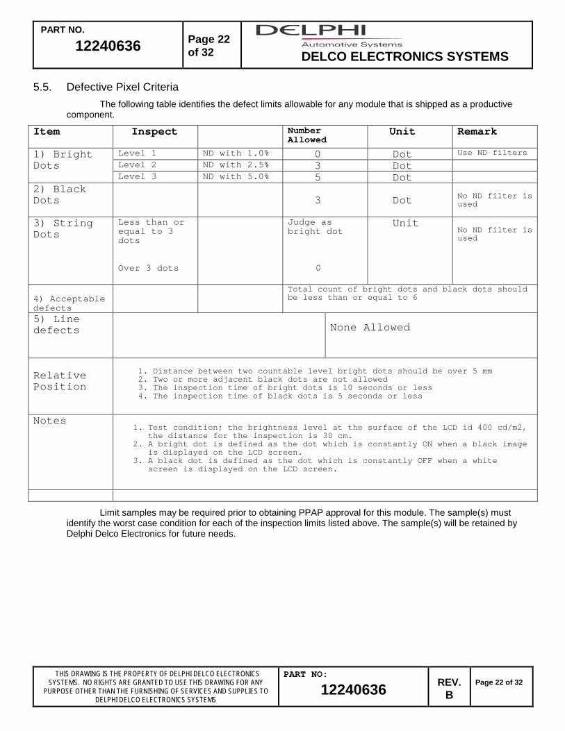
5.5. Defective Pixel Criteria
The following table identifies the defect limits allowable for any module that is shipped as a productivecomponent.
Item Inspect NumberAllowed
Unit Remark
Level 1 ND with 1.0% 0 Dot Use ND filters
Level 2 ND with 2.5% 3 Dot1) BrightDots
Level 3 ND with 5.0% 5 Dot2) BlackDots 3 Dot No ND filter is
used
3) StringDots
Less than orequal to 3dots
Over 3 dots
Judge asbright dot
0
UnitNo ND filter isused
4) Acceptabledefects
Total count of bright dots and black dots shouldbe less than or equal to 6
5) Linedefects None Allowed
RelativePosition
1. Distance between two countable level bright dots should be over 5 mm2. Two or more adjacent black dots are not allowed3. The inspection time of bright dots is 10 seconds or less4. The inspection time of black dots is 5 seconds or less
Notes1. Test condition; the brightness level at the surface of the LCD id 400 cd/m2,
the distance for the inspection is 30 cm.2. A bright dot is defined as the dot which is constantly ON when a black image
is displayed on the LCD screen.3. A black dot is defined as the dot which is constantly OFF when a white
screen is displayed on the LCD screen.
Limit samples may be required prior to obtaining PPAP approval for this module. The sample(s) mustidentify the worst case condition for each of the inspection limits listed above. The sample(s) will be retained byDelphi Delco Electronics for future needs.

PART NO.
12240636 Page 23of 32 DELCO ELECTRONICS SYSTEMS
THIS DRAWING IS THE PROPERTY OF DELPHI DELCO ELECTRONICS SYSTEMS. NO RIGHTS ARE GRANTED TO USE THIS DRAWING FOR ANY
PURPOSE OTHER THAN THE FURNISHING OF SERVICES AND SUPPLIES TO DELPHI DELCO ELECTRONICS SYSTEMS
PART NO:
12240636REV.
BPage 23 of 32
5.6. Cosmetic Defects:
Spot Defects as a function of diametric size100um > d Any quantity allowed, but must not be connected100um < d < 300um A total of (2) allowed per display300um < d (0) allowed per display
Line defects as a function of line width (W) and length (L)W< 40um, L < 100 um Any quantity allowed, but must NOT be connected100 um < L < 2000um, W <40um (2) allowed per displayL > 2000um, W > 40um (0) allowed per display
Bubble Defects as a function of diametric size150um > d Any quantity allowed, but must NOT be connected150um < d < 300um (2) allowed per display300um < d < 500um (1) allowed per display500um < d (0) allowed per display
Scratches on the PolarizerL < 10 mm N < 3
Dent on Polarizer0.1 mm < D < 0.5 mm N < 3
5.7. Polarizer Definition:
Front: PFILZ3223TPZZ
Back: PFILZ3224TPZZ
Manufacturer: SANRITZ
Matte Finish: AG (Front Only)
The polarizer configuration will be such as to allow viewing of the display with polarizing sunglasses.

PART NO.
12240636 Page 24of 32 DELCO ELECTRONICS SYSTEMS
THIS DRAWING IS THE PROPERTY OF DELPHI DELCO ELECTRONICS SYSTEMS. NO RIGHTS ARE GRANTED TO USE THIS DRAWING FOR ANY
PURPOSE OTHER THAN THE FURNISHING OF SERVICES AND SUPPLIES TO DELPHI DELCO ELECTRONICS SYSTEMS
PART NO:
12240636REV.
BPage 24 of 32
6. PRODUCT ASSURANCE PROVISIONS
6.1. Screening
The supplier shall perform the necessary screens to assure that each part conforms to the requirementsherein. The intent of this specification is to insure the correct operation of each part throughout the applicablewarranty of the vehicle in which it is installed.
Refer to paragraph 6.3, Quality Conformance Inspection, for a lot acceptance procedure.
6.2. Electrical and Optical Testing
Production modules must be tested at 25 +/- 5°C to assure they meet all the requirements of thisspecification prior to shipment or assured by design. Electrical connections to the module utilized for testing mustbe made through the appropriate connector(s). The exact test method and sequence is to be supplied with thePPAP documentation. Changes to the production test method or sequence must be approved by Delphi-D prior toimplementation.
6.3. Quality Conformance Inspection
To be performed by the supplier of the display.

PART NO.
12240636 Page 25of 32 DELCO ELECTRONICS SYSTEMS
THIS DRAWING IS THE PROPERTY OF DELPHI DELCO ELECTRONICS SYSTEMS. NO RIGHTS ARE GRANTED TO USE THIS DRAWING FOR ANY
PURPOSE OTHER THAN THE FURNISHING OF SERVICES AND SUPPLIES TO DELPHI DELCO ELECTRONICS SYSTEMS
PART NO:
12240636REV.
BPage 25 of 32
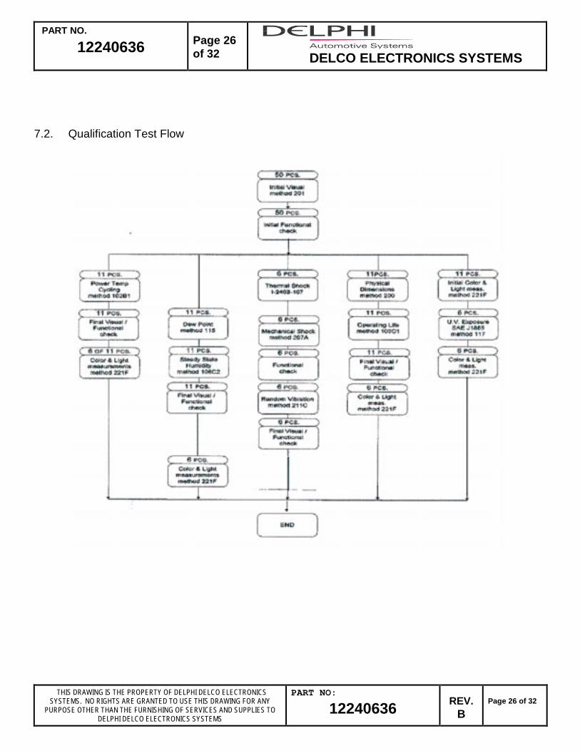
7. QUALIFICATION TESTING
7.1. Qualification Test Methods
The Qualification test methods for this module are given in the table below and are taken from the ComponentSpecification for Liquid Cryslal Display Modules rev.A) C-5007, Table 1. The qualification testing is responsibility ofthe supplier and must be performed in a Delphi SQ1000 approved test laboratory.The electrical endpoints shall beperformed per C-5007.
Method Condition Description
Q-1000-102* B1 (See Note 1) Power Temperature CyclingQ-1000-103 C1(See Note 1) Operating LifeQ-1000-106 B3(See Note 2) Steady State HumidityQ-1000-115 - Dew PointQ-1000-117(SAEJ1885) C3 Ultraviolet ExposureQ-1000-200 (See Note 3) Physical DimensionsQ-1000-201 (See Note 3) External VisualQ-1000-207 A (See Note 1) Mechanical ShockQ-1000-211 C (See Note 1) Vibration-RandomQ-1000-221 F Color MeasurementQ-1000-301 - ESD Sensitivity Charged Device ModelC-5007, 7.1.1 - Functional TestC-5007, 7.3.1 - Low Temperature Response TimeC-5007, 7.3.2 - Contrast Ratio at TemperatureI-2403-107 (See Note 4) Thermal ShockDE Standard (See Note 5 and Figure 7.3) Electromagnetic Compatibility
10949001 Material SpecificationSubstances of Concern andRecycled Content
Notes:
* Backlighting and power may be disabled during temperatures below -30ºC and above +70ºC.
1. Refer to Part Drawing for electrical bias and operating conditions
2. Except, 60°C (± 2) and 90% (± 5) R.H. for 300 hours.
3. In addition to Q-1000-201, samples shall be evaluated for labeling and cosmetic defects as specified inSection 5.5 and Delphi Delco Electronics Systems Component Spec C-5007.
4. Delphi Delco Electronics Systems work instruction procedure.
5. DE Standard EMC Tests will be performed by Delphi at the final assembly/end model part number level.This module may not be a root cause for failure of the end model assembly during these tests or be thesource of EMI such the end model fails customer’s requirements for Electromagnetic Compatability.
PART NO.
12240636 Page 26of 32 DELCO ELECTRONICS SYSTEMS
THIS DRAWING IS THE PROPERTY OF DELPHI DELCO ELECTRONICS SYSTEMS. NO RIGHTS ARE GRANTED TO USE THIS DRAWING FOR ANY
PURPOSE OTHER THAN THE FURNISHING OF SERVICES AND SUPPLIES TO DELPHI DELCO ELECTRONICS SYSTEMS
PART NO:
12240636REV.
BPage 26 of 32
7.2. Qualification Test Flow

PART NO.
12240636 Page 27of 32 DELCO ELECTRONICS SYSTEMS
THIS DRAWING IS THE PROPERTY OF DELPHI DELCO ELECTRONICS SYSTEMS. NO RIGHTS ARE GRANTED TO USE THIS DRAWING FOR ANY
PURPOSE OTHER THAN THE FURNISHING OF SERVICES AND SUPPLIES TO DELPHI DELCO ELECTRONICS SYSTEMS
PART NO:
12240636REV.
BPage 27 of 32
7.3. Endpoint Requirements
Parameters or measurements to be taken and recorded on test samples at specified endpoints throughout thequalification testing process. In the event samples can not be visually monitored during environmental tests, endpoints shall be taken at the mid point of test hours. All measurements must be within the print or test method’sspecified limits.
7.3.1. Initial / Final Visual:a. Evaluate per Q-1000-201 and Section 5.0.
7.3.2. All Functional Checks, Initial, Final, Intermediate, ect.a. All viewing modes per Section 3.7.b. Backlight circuit functionality per Sections 3.8, 5.1.c. Displays a test pattern on all selectable inputs per Section 3.6.
7.3.3. Power Temperature Cyclinga. Measure and record backlight temperature performance to 50% nominal brightness at -30C before
and after PTC test.b. Perform final visual.c. Perform final functional.
7.3.4. Operating Lifea. Perform final visual.b. Perform final functional.
7.3.5. Steady State Humiditya. Perform final visual.b. Perform final functional.
7.3.6. Dew Pointa. Evaluate per Q-1000-115 requirements.
7.3.7. UV Exposurea. Evaluate per color and light end point requirements.
7.3.8. Physical Dimensionsa. Measure and record all overall dimensions referenced on the part drawing.b. Measure and record mounting hole dimensions.
7.3.9. Thermal Shocka. Perform functional check.
7.3.10. Mechanical Shocka. Perform functional check.b. Inspect for and note any mechanical damage.
PART NO.
12240636 Page 28of 32 DELCO ELECTRONICS SYSTEMS
THIS DRAWING IS THE PROPERTY OF DELPHI DELCO ELECTRONICS SYSTEMS. NO RIGHTS ARE GRANTED TO USE THIS DRAWING FOR ANY
PURPOSE OTHER THAN THE FURNISHING OF SERVICES AND SUPPLIES TO DELPHI DELCO ELECTRONICS SYSTEMS
PART NO:
12240636REV.
BPage 28 of 32
7.3.11. Random Vibrationa. Evaluate per functional check.b. Inspect for and note mechanical damage.
7.3.12. Color and Lighta. Measure and record optical requirements per section 5.1 , except response time.b. Evaluate samples for defective pixel criteria per section 5.5.

PART NO.
12240636 Page 29of 32 DELCO ELECTRONICS SYSTEMS
THIS DRAWING IS THE PROPERTY OF DELPHI DELCO ELECTRONICS SYSTEMS. NO RIGHTS ARE GRANTED TO USE THIS DRAWING FOR ANY
PURPOSE OTHER THAN THE FURNISHING OF SERVICES AND SUPPLIES TO DELPHI DELCO ELECTRONICS SYSTEMS
PART NO:
12240636REV.
BPage 29 of 32
8. PACKAGING METHOD FOR SHIPMENT
8.1. Packaging Drawing

PART NO.
12240636 Page 30of 32 DELCO ELECTRONICS SYSTEMS
THIS DRAWING IS THE PROPERTY OF DELPHI DELCO ELECTRONICS SYSTEMS. NO RIGHTS ARE GRANTED TO USE THIS DRAWING FOR ANY
PURPOSE OTHER THAN THE FURNISHING OF SERVICES AND SUPPLIES TO DELPHI DELCO ELECTRONICS SYSTEMS
PART NO:
12240636REV.
BPage 30 of 32

PART NO.
12240636 Page 31of 32 DELCO ELECTRONICS SYSTEMS
THIS DRAWING IS THE PROPERTY OF DELPHI DELCO ELECTRONICS SYSTEMS. NO RIGHTS ARE GRANTED TO USE THIS DRAWING FOR ANY
PURPOSE OTHER THAN THE FURNISHING OF SERVICES AND SUPPLIES TO DELPHI DELCO ELECTRONICS SYSTEMS
PART NO:
12240636REV.
BPage 31 of 32
9. APPLICATION NOTES
9.1. Protective Film
The LCD module is shipped with a clear protective film over the LCD to prevent scratches during shippingand handling. This film should be removed as late as possible in the assembly process to prevent damageoccurring to the LCD polarizer. Peel the film slowly (more than 3 seconds) from the edge and back upon itself toprevent ESD damage. An air ionizer is necessary.
9.2. LCD Cleaning
When and if cleaning of the LCD is necessary use a soft absorbent lint free cotton cloth with a smallamount of Ethanol.
9.3. Mechanical Stress
Do not bend or twist the module during assembly or fixture the module in a method by a means other thanit has been designed for. Pressure on the LCD may cause the glass to crack and/or the cell gap distance tochange altering the LCD visual performance.

PART NO.
12240636 Page 32of 32 DELCO ELECTRONICS SYSTEMS
THIS DRAWING IS THE PROPERTY OF DELPHI DELCO ELECTRONICS SYSTEMS. NO RIGHTS ARE GRANTED TO USE THIS DRAWING FOR ANY
PURPOSE OTHER THAN THE FURNISHING OF SERVICES AND SUPPLIES TO DELPHI DELCO ELECTRONICS SYSTEMS
PART NO:
12240636REV.
BPage 32 of 32
REVISION HISTORY
DATE SYM REVISION RECORD PDRC/CA DR. CK
18NO03 A Release Production Per CN32258 172857 MRV SVN06FE04 B C23 in module changed from 1000pF to 1uF to eliminate display flicker.
Per CN35150.179823 SVN SMA