ORIGINAL LITERARY WORK DECLARATION -...
24
UNIVERSITI MALAYA ORIGINAL LITERARY WORK DECLARATION Name of Candidate: MAASPALIZA BINT AZRI (LC/Passport No: 770618-04-5114) Registration/Matric No: KHA 090044 Name of Degree: DOCTOR OF PHILOSOPHY Title of Project Paper/Research Report/Dissertation/Thesis ("this Work"): COMPARISON OF SINGLE-PHASE TRANSFORMERLESS PHOTOVOLTAIC GRID- CONNECTED INVERTER TOPOLOGIES WITH HIGH EFFICIENCY AND LOW GROUND LEAKAGE CURRENT Field of Study: POWER ELECTRONICS I do solemnly and sincerely declare that: ( 1) I am the sole author/writer of this Work; (2) This Work is original; (3) Any use of any work in which copyright exists was done by way of fair dealing and for permitted purposes and any excerpt or extract from, or refer3nce to or reproduction of any copyright work has been disclosed expressly and sufficiantly and the title of the Work and its authorship have been acknowledged in this Work; (4) I do not have any actual knowledge nor do I ought reasonablv to know that the making of this work constitutes an infringement of any copyright work; (5) I hereby assign all and every rights in the copyright to this Work to the University of Malaya ("UM"), who henceforth shall be owner of the copyright in this Work and that any reproduction or use in any form or by any means whatsoever is prohibited without the written consent of UM having been first had and obtained; (6) I am fully aware that if in the course of making this Work I h&ve infringed any copyright whether intentionally or otherwise, I may be subject to legal action or any other action as may be determined by UM. Candidate's Signature ,hf Subscribed Witness's Sig ature Name: Designation: Dr. Che Han1 Senc Pensyarah Kanan UMPEDAC, Universitl Malaya Date G(l I 1015 Date 6(1 /
Transcript of ORIGINAL LITERARY WORK DECLARATION -...
UNIVERSITI MALAYA
ORIGINAL LITERARY WORK DECLARATION
Name of Candidate: MAASPALIZA BINT AZRI (LC/Passport No: 770618-04-5114)
Registration/Matric No: KHA 090044
Name of Degree: DOCTOR OF PHILOSOPHY
Title of Project Paper/Research Report/Dissertation/Thesis ("this Work"):
COMPARISON OF SINGLE-PHASE TRANSFORMERLESS PHOTOVOLTAIC GRIDCONNECTED INVERTER TOPOLOGIES WITH HIGH EFFICIENCY AND LOW GROUND
LEAKAGE CURRENT
Field of Study: POWER ELECTRONICS
I do solemnly and sincerely declare that:
( 1) I am the sole author/writer of this Work; (2) This Work is original; (3) Any use of any work in which copyright exists was done by way of fair dealing and for
permitted purposes and any excerpt or extract from, or refer3nce to or reproduction of any copyright work has been disclosed expressly and sufficiantly and the title of the Work and its authorship have been acknowledged in this Work;
(4) I do not have any actual knowledge nor do I ought reasonablv to know that the making of this work constitutes an infringement of any copyright work;
(5) I hereby assign all and every rights in the copyright to this Work to the University of Malaya ("UM"), who henceforth shall be owner of the copyright in this Work and that any reproduction or use in any form or by any means whatsoever is prohibited without the written consent of UM having been first had and obtained;
(6) I am fully aware that if in the course of making this Work I h&ve infringed any copyright whether intentionally or otherwise, I may be subject to legal action or any other action as may be determined by UM.
Candidate's Signature
,hf Subscribed an~n
Witness's Sig ature
Name: Designation:
Dr. Che Han1 Senc Pensyarah Kanan UMPEDAC, Universitl Malaya
Date G(l I 1015
Date 6(1 / ;r<:>I~
Abstract
When a transformer is taken out of a photovoltaic (PV) inverter system, the
efficiency of the whole system can be improved. Unfortunately, the additional ground
leakage current appears and needs to be considered. The problem of ground leakage current
is that it poses an electrical hazard to anyone touching the photovoltaic (PV) array's
surface. For safety issues, the ground leakage current should be less than 300 mA, which
follows the VDE-0126-1-1 German standard. To minimize the ground leakage current in
the transformerless PV grid connected inverter system, the proposed inverter topologies
(SC-HB inverter, bipolar H-Bridge inverter with CD-Boost converter, modified unipolar H
Bridge inverter with CD-Boost converter and modified unipolar H-Bridge inverter with
modified boost converter) are analyzed, verified and compared in this thesis. In order to
analyze the effect of unbalanced filter inductance on the transformerless bipolar H-Bridge
inverter topology, the matching ratio of inductance :Lr = Lfl/Lfln and L12IL12n ) is
investigated. In addition, the effect of parasitic capacitance value on the transformerless
bipolar H-Bridge inverter topology is studied. The effect of modulation techniques using
bipolar SPWM and unipolar SPWM on the transformerlcss H-Bridge inverter topology is
compared and analyzed in terms of common-mode voltage and ground leakage current.
TMS320F28 I 2 is used as a controller to generate the PWM control signal, maximum
power point tracking (MPPT) based on power balance and Proportional-Integral (PI)
controller. PSIM 9.0 simulation software is used to design the proposed transformerless
inverter topologies. Simulation and experimental results verified the proposed inverter's
feasibility in addressing issues of transformerless DC/ AC converters in grid-connected PV
systems.
ii

Abstrak
Apabila pengubah diambil daripada sistem photovoltaic (PV) penyongsang,
kecekapan keseluruhan sistem boleh diperbaiki. Malangnya, tambahan arus kebocoran
bumi akan muncul dan perlu dipertimbangkan. Masalah kebocoran arus bumi ialah ia
menimbulkan bahaya elektrik kepada sesiapa menyentuh permukaan photovoltaic (PV)
array. Untuk isu-isu keselamatan, kebocoran arus bumi hendaklah tidak kurang daripada
300 mA, yang mengikuti VDE-0126-1-1 standard Jermar. Untuk mengurangkan arus bocor
bumi di grid yang berkaitan sistem penyongsang ~engubah PV, topologi-topologi
penyongsang dicadangkan (penyongsang SC-HB, penyongsang bipolar H-Bridge dengan
penukar CD-Boost, penyongsang modified unipolar H-Bridge dengan penukar CD-Boost
dan penyongsang modified unipolar H-Bridge dengan penukar modified boost) dianalisis
dan disahkan di dalam tesis ini. Untuk menganalisis kesan tidak seimbang penapis
kearuhan pada pengubah bipolar H-Bridge penyongsang topologi, nisbah kearuhan (Lr =
Lf!/Lf!n dan Lf2/LJ2n) disiasat. Juga, kesan nilai kapasitan parasit pada pengubah bipolar H
Bridge penyongsang topologi dikaji. Kesan teknik modulasi (SPWM bipolar dan SPWM
unipolar) pada pengubah H-Bridge penyongsang topologi dibandingkan dan dianalisis dari
segi common-mode voltan dan arus bumi bocor. TMS320F2812 digunakan sebagai
pengawal untuk menjana isyarat lebar denyut modulasi, maksimum pengesanan titik kuasa
berdasarkan pembahagian kuasa dan kawalan Berkadar-Integral. Perisian simulasi PSIM
9.0 digunakan untuk merekabentuk topologi-topologi penyongsang pengubah yang
dicadangkan. Keputusan simulasi dan ujikaji mengesahkan bahawa cadangan penyongsang
memenuhi isu-isu yang berkaitan dengan penukar Arns Terus/Arus Ulang-Alik (AT/AU) di
dalam sistem penyambungan PV ke grid.
iii

ACKNOWLEDGEMENT
In the name of Allah, the most Gracious and most Compassionate.
I would like to thank Allah The Almighty for blessing and giving me strength to
accomplish this thesis. Special thanks to my supervisor, Prof. Dr. Nasrudin Abd.
Rahim for his invaluable support, encouragement, supervision and useful suggestions
throughout this project. His moral support and contim.ous guidance enabled me to go
through the tough route to complete this project successfully.
I acknowledge my sincere indebtedness and gratitude to my beloved husband, Nazarul
Abidin Ismail, my sons, Aizuddin Nasru!Haq, Ahmad Naqiuddin and Aaqil Najmuddin for
his love, support and sacrifice throughout my toughest time in my life. My deepest
gratitude for my friends for consistently encouraged me and keep my heart strong in
accomplish this PhD study. I cannot find the appropriate words that could properly describe
my appreciation for their devotion, support and faith in my ability to attain my goals.
Finally, I acknowledge my greatest thanks to University cf Malaya and Universiti Teknikal
Malaysia Melaka (UTeM) for all support given to complete this project.
iv
ABSTRACT
ABSTRAK
ACKNOWLEDGEMENTS
TABLE OF CONTENTS
LIST OF FIGURES
LIST OF TABLES
LIST OF SYMBOLS
TABLE OF CONTENTS
LIST OF ABBREVIATIONS
CHAPTER 1: INTRODUCTION
I. I Background
I .2 Objectives
1.3 Methodology and Scope of Study
1.4 Thesis Organization
CHAPTER 2: SOLAR PV SYSTEMS
2.1 Introduction
2.2 Photovoltaic Module
2.2.l Types of PV Cell
2.2.2 Operation of PV Cell
2.2.3 PV Modules Behaviour
2.2.3.1 Series PY Modules
2.2.3.2 Parallel PY Modules
11
iii
IV
v
xii
xxiii
XXIV
XXVll
6
7
8
10
10
11
12
12
14
15
v

2.2.3.3 Series-Parallel PV Modules 16
2.3 PV Inverter Connection Systems 17
2.3.1 Stand Alone system 17
2.3.2 Grid-Connected system 19
2.3.2.1 SEDA Malaysia Feed in Tariff (FiT) Mechanism 20
2.3.3 Hybrid system 21
2.4 PV Inverter Systems 22
2.4.1 Sizing 22
2.4.2 Types of grid-connected PV inverter 24
2.4.2.1 Central Inverters 24
2.4.2.2 String Inverters 24
2.4.2.3 Module- Integrated Inverter 26
2.4.2.4 Multi-String Inverter 26
2.5 PV grid-connected Inverter Configurations 27
2.5.1 Line Frequency Transformer 27
2.5.2 High Frequency Transformer 28
2.5.3 Transformer-less/without Transformer 29
2.6 Maximum Power Point Tracker (MPPT) Algorithms 30
2.6.1 Constant Voltage 30
2.6.2 Perturbation and observation (P&O) 31
2.6.3 Incremental Conductance (IC) 32
2.7 Protection for Grid-Connected PV Inverters 33
2.8 Power Quality Issues 35
2.8. l Harmonics 35
2.8.2 Total Harmonics Distortion (THD) 35 VI

2.8.3 Power Factor of PV inverter
2.9 Performance PV inverter issues
2.10 Summary
CHAPTER 3: OVERVIEW OF POWER CONVERTER PHOTOVOLTAIC
SYSTEM
3.1 Introduction
3.2 Power Converter
3.3 Types of Non-Isolated DC-DC Converters Commrnly Used
3.3. l Non Isolated DC-DC Converters
3.3.1.1 Conventional DC-DC Boost Converter
3.3.1.2 Cuk-Derived Boost (CD-boost) Converter
3.3.1.3 Three-level DC-DC Boost Conve1ter
3.3.1.4 Cascaded DC-DC Boost Convertt::r
3.3.1.5 Inverting Zeta Derived DC-DC Converter
3.4 Pulse Width Modulation (PWM) Scheme
3.4.1 PWM based Voltage Forced Strategy
3.5 PV Inverter Topologies
3.6 Parasitic capacitance of PV System
3.7 Ground Leakage Current in Transformerless PV Grid-Connected System
3.8 Transformerless Single-Phase H-Bridge Inverter L>pology
3.9 Common-Mode Voltage model in Transformerless PV H-Bridge Inverter System
3.10 Fourier Analysis of the Common-Mode Voltage
36
37
38
40
40
41
41
42
44
45
47
48
49
50
51
51
53
54
57
60
Vil

3.11 Modified Transformerless Single-phase H-Bridge Inverter Topologies 61
3.12 HERIC Topology 62
3.13 HB-ZVR Topology 63
3.14 H6 Topology 64
3.15 HS Topology 65
3.16 oH5 Topology 66
3.17 Half Bridge Topology 67
3.18 Neutral Point Diode Clamped (NPC) Topology 67
3.19 Filter configuration and Ground Leakage Current 68
3.20 Comparison of Transformerless Single-Phase H-Bridge Inverter Topologies 69
3.21 Single-Phase Multilevel Inverter Topologies 74
3.22 Module Integrated Converter (MIC) Topologies 77
3.23 Summary 80
CHAPTER 4: PROPOSED SINGLE-PHASE TRANSFORMERLESS
VOLTAGE SOURCE INVERTER
4.1 Introduction 81
4.2 Block diagram of the Proposed Single-phase Transformerless PV Grid- Connected System 81
4.3 Conventional Transformerless H-Bridge inverter 83
4.4 Filter Design 88
4.5 Configuration of Proposed Split Capacitor H-Bridge (SC-HB) Inverter with Balancing Circuit 90
4.5.1 The Balancing Strategy in SC-HB Inverter 91
4.5.2 Ground Leakage Current Reduction in Proposed SC-HB Inverter Topology 93
viii

4.6 Proposed Bipolar H-Bridge inverter with CD-Boost Converter 95
4.6.1 Power Decoupling Calculation 96
4.6.2 Cuk-Derived Boost (CD-Boost) Converter 97
4.6.3 Proposed Modified Unipolar H-Bridge Imerter with CD-Boost Converter 100
4.6.3.1 Switching Strategy of Modified Unipolar H-Bridge Inverter with CD-Boost Converter 101
4.6.3.2 Mode of Operation for Modified Unipolar H-Bridge Inverter with CD-Boost Converter 101
4.7 Proposed Modified DC-DC Converter with Low Input Current Ripple
103 4.8 Proposed Modified Unipolar H-Bridge Inverter with Modified Boost
Converter 107
4.8.l Mode Operation of Proposed Unipolar H-Bridge Inverter with Modified Boost Converter 107
4.9 Power Balancing Controller 109
4.10 Anti-islanding Protection 109
4.11 Summary 110
CHAPTER 5: SIMULATION RESULTS
5.1 Introduction 113
5.2 Simulation of Single-Phase H-Bridge Inverter 113
5.3 Proposed SC-HB Configuration 122
5.4 Conventional Boost converter and CD-Boost Converter 126
5.5 Proposed Bipolar H-Bridge inverter with CD-Boost Converter 129
5.6 Proposed Modified unipolar H-Bridge inverter wit!1 DC-Boost Converter 132
5.7 Proposed Modified Unipolar H-Bridge Inverter with Modified Boost Converter 136
5.8 Summary 139 ix

CHAPTER 6: EXPERIMENTAL RESULTS
6.1
6.2
6.3
6.4
6.5
6.6
6.7
6.8
6.9
Introduction
Hardware Configuration
Experimental Results
6.3.1 Non-Isolated DC-DC Boost Converter
6.3 .2 Ripple of Input DC Current
6.3.3 Comparison for Various Non-Isolated DC.-DC Boost Converter
Experimental Results of Single-Stage H-Bridge Inv~rter Topologies
140
140
143
143
148
151
154
6.4.1 Conventional Unipolar and Bipolar H-Bridge Inverter Topology 154
6.4.2 Effect of Filter Impedance Matching and Parasitic Capacitance to Ground Leakage Current in Bipolar H-Bridge Inverter 159
6.4.3 HB-ZVR Inverter Topology 162
6.4.4 Proposed SC-HB Inverter Topology 164
Experiment Results of Proposed Two-Stage Inver:er System 167
6.5.1 Proposed Bipolar H-Bridge Inverter with CD-Boost Converter 167
6.5.2 Proposed Modified Unipolar H-Bridge Inverter with CD-Boost Converter 170
6.5.3 Proposed Modified Unipolar H-Bridge Imerter with Modified Boost Converter 173
Performance Comparisons for Various Inverters 174
Controlling Algorithm for MPPT 178
Anti-islanding 179
Summary 180
x
CHAPTER 7: CONCLUSION AND FUTURE WORKS
7.1 Concluding Remarks
7.2 Author's Contribution
7.3 Future Works
REFERENCES
APPENDICES
APPENDIX A
APPENDIXB
APPENDIXC
Hardware Experimental Set-up
Code Generation in TMS32F2812 DSP
Summary of Relevant Published wcrk by the Author
181
183
184
185
A.I
B.1
C.l
XI

LIST OF FIGURES
Figure 1.1 Growth of Worldwide Energy Production Since 1970 to 2025 (Wikipedia.org)
Figure 1.2 World Total Electricity Production from Renewable Sources in 2011 (IEA International Energy Agency, 2010) 2
Figure 1.3 Solar PY Global Capacity 1995-2012 (RE\f21, 2013) 3
Figure 1.4 The world major inverter manufacturer in 2005 (Report Milestone, 2005) 4
Figure 1.5 The effect of isolating transformers to European inverter efficiency (Schlumberger, 2007) 6
Figure 2.1 Photovoltaic cells, modules, panels and anays 1 1
Figure 2.2 Types of Silicon PY Cells 11
Figure 2.3 Representation of PY modules in circuit diagram 13
Figure 2.4 Single PY module characteristic curve 13
Figure 2.5 Series connection of PY modules 14
Figure 2.6 Series PY module connection IV curve 14
Figure 2.7 Parallel connection of PY modules 15
Figure 2.8 I-V Parallel PY Modules curve 15
Figure 2.9 Series-parallel connection of PY module 16
Figure 2.10 I-V curve for series-parallel configuration ( Chetan, 2011) 16
Figure 2.11 Stand-alone PY system (Chetan, 2011) 17
Figure 2.12 PY direct conversion 18
Figure 2.13 PY interactive conversion 18
Figure 2.14 PY on-line conversion 18
Figure 2.15 PY parallel coordinated conversion 19
Figure 2.16 Grid-connected PY system (Chetan, 2011) 20
Xll

Figure 2.17 Hybrid PY system (Electricity Resources Branch, 2011) 22
Figure 2.18 Central inverter connection 25
Figure 2.19 String inverter connection 25
Figure 2.20 Module integrated inverter configuration 26
Figure 2.21 Multistring inverter configuration 27
Figure 2.22 Single-phase multistring five-level inverter topology 28
Figure 2.23 PY inverter with DC-DC converter and HF transformer 29
Figure 2.24 PY transformerless H-Bridge inverter system 30
Figure 2.25 Perturbation and observation MPPT technique 32
Figure 2.26 Incremental Conductance MPPT flowchart method 33
Figure 2.27 Islanding detection methods 34
Figure 3.1 Types of DC to AC converter 40
Figure 3.2 DC-DC converter block diagram 40
Figure 3.3 General block diagram of AC to DC conveiter 41
Figure 3.4 General block diagram of AC to AC converter 41
Figure 3.5 The DC-DC boost converter 42
Figure 3.6 Boost converter waveform (a) Inductor vohage, (b) Inductor current 43
Figure 3.7 The CD- Boost converter circuit 44
Figure 3.8 Three level DC-DC boost converter 46
Figure 3.9 Switching pattern and inductor voltage wa\eform of three-level converter; (a)(~< Vc/2), (b) (~>Vc/2). 47
Figure 3.10 Cascaded DC-DCboost converter 48
Figure 3.11 Inverting zeta derived boost converter 49
Figure 3 .12 Principle of sinusoidal PWM technique 50
Figure 3.13 The top and cross-section view of PY module with mounting frame 52
Xlll

Figure 3.14 Detail cross-section of PV module. 53
Figure 3.16 Single-phase transformerless inverter with parasitic capacitance 55
Figure 3.17 Output inverter voltage (Vab) using unipolar PWM technique 56
Figure 3.18 Output inverter voltage (Vab) using bipolar PWM technique 56
Figure 3.19 The common-mode model for the PWM voltage source inverter system 58
Figure 3.20 Simplified equivalent model of common-mode resonant circuit 59
Figure 3.21 Equivalent circuit for the common-mode leakage current path 60
Figure 3.22 HERIC topology 63
Figure 3.23 HB-ZVR topology 64
Figure 3.24 H6 topology (German Patent, 2003) 65
Figure 3.25 H5 topology 66
Figure 3.26 oH5 topology (Huafeng et al., 2011) 66
Figure 3.27 Half bridge inverter topology 67
Figure 3.28 NPC inverter topology 68
Figure 3.29 (a) LCL filter configuration case (1), (b) LCL filter configuration case (2) 69
Figure 3.30 (a) Common-mode voltage and (b) ground leakage when unipolar PWM technique is used 70
Figure 3.31 (a) Common-mode voltage and (b) leakage when bipolar PWM technique is used 71
Figure 3.32 Common-mode voltage and leakage ground current in case of HERIC topology 72
Figure 3.33 Common-mode voltage and leakage ground current in case of HB-ZVR topology 72
Figure 3.34 Common-mode voltage and leakage ground current in case of H6 topology 73
xiv

Figure 3.35 Common-mode voltage and leakage ground current in case of H5 topology 73
Figure 3.36 Common-mode voltage and leakage ground current in case of oH5 topology 73
Figure 3.37 Transformerless multilevel cascade inverter (F. Peng at el., 1996) 75
Figure 3.38 Single phase five level diode clamped inve1ter topology (Manjrekar M.D & Lipo T.A, 1998) 76
Figure 3.39 Flying capacitor topology (Hung and Corzine, 2006) 76
Figure 3.40 Multistring five-level single phase inverter (Rahim et al. 2010) 77
Figure 3.41 MIC arrangement 77
Figure 3.42 Grid-Connected PV System using two energy processing stages (Martin & Demonti, 2002) 78
Figure 3.43 Modified inverter configuration (Saha et al , 1998) 78
Figure 3.44 Two-stage photovoltaic grid- connected inYerter (Chomsuwans et al.2002) 78
Figure 3.45 Buck-boost-operation-based sinusoidal inverter circuit (Funabiki et al, 2002) 79
Figure 3.46 Transformerless PV inverter with DC-DC boost converter 79
Figure 3.47 DC-AC boost inverter (Caceres and Barbi, 1999) 80
Figure 4.1 Block diagram of the proposed transformerless PV grid-connected system 82
Figure 4.2 Conventional transformerless H-Bridge inverter 83
Figure 4.3 Half-positive cycle state for H-Bridge circ1it (state I) 84
Figure 4.4 Zero state for half-positive cycle (state II) 85
Figure 4.5 Zero state for half-positive cycle (state III) 85
Figure 4.6 Positive cycle state for bipolar H-Bridge inverter circuit 87
Figure 4.7 Negative cycle state for bipolar H-Bridge inverter circuit 87
Figure 4.8 LCL configuration for the proposed transformerless PV system 89
xv

Figure 4.9 SC-HB transformerless inverter topology 90
Figure 4.10 (a) The balancing circuit, (b) energy transfer from CBI to CB2; (c) energy transfer from CB2 to CBI 92
Figure 4.11 Mode operation of SC-HB topology, (a) zero positive state (b) positive active 94
Figure 4.12 The proposed bipolar H-Bridge inverter with CD-Boost converter for grid-connected PV system 96
Figure 4.13 The CD- Boost converter circuit 99
Figure4.14 Operation modes of the CD-Boost converter (a) switch-on mode, (b) switch-off mode 99
Figure 4.15 Modified unipolar H-Bridge inverter with CD-Boost converter 100
Figure 4.16 Active vector state applied to grid (mode l) 102
Figure 4.17 Zero vector state applied to grid (mode 2) 103
Figure 4.18 (a) Proposed modified boost converter circuit, (b) switch tum-on mode, ( c) switch tum-off mode 104
Figure 4.19 Modified Unipolar H-Bridge inverter with modified boost converter circuit configuration 107
Figure 4.20 Active vector state mode, applied to grid for proposed unipolar H-Bridge inverter with modified boost converter 108
Figure 4.21 Zero vector state mode, applied to grid for proposed unipolar H-Bridge inverter with modified boost converter 109
Figure 4.22 Flow chart of power balancing control 111
Figure 4.23 Flow chart of anti-islanding algorithm 112
Figure 5.1 (a) Simulation set up for the single-phase transformerless H-Bridge inverter, (b) LCL filter configuration 114
Figure 5.2 (a) Hybrid modulation technique of single··phase H-Bridge inverter, (b) unipolar modulation technique of single-phase H-Bridge inverter 116
Figure 5.2 ( c) Bipolar modulation technique of single-phase H-Bridge inverter 117
xvi

Figure 5.3
Figure 5.3
Figure 5.4
Figure 5.4
Figure 5.5
Figure 5.5
Figure 5.6
Figure 5.7
Figure 5.7
Figure 5.8
Figure 5.9
H-Bridge inverter output voltage for (a) hybrid & unipolar modulation technique
H-Bridge inverter output voltage for (b) unipolar modulation technique
Common-mode voltage ofH-Bridge inverter for (a) hybrid & unipolar modulation technique
Common-mode voltage ofH-Bridge invener for (a) bipolar modulation technique
Ground leakage current of H-Bridge inverter for (a) bipolar modulation technique
Ground leakage current of H-Bridge inverter for (b) unipolar modulation technique
Simulated harmonic spectra of the commor-mode voltage of the (a) unipolar and (b) bipolar SPWM techniques
(a) Shematic diagram of SC-HB configuratlon
(b) balancing circuit
(a) Capacitor voltage (VcBl & Vcm) without '.)alancing circuit, (b) Capacitor voltage (Vcs1 & Vcm) with bal lncing circuit
Simulation results of proposed SC-HB inverter topology; (a) common-mode voltage (Vcmm), (b) ground leakage current (lg)
117
118
118
119
119
120
121
122
123
124
125
Figure 5.10 S1 & S2 switching, imbalance de link series capacitor voltages (VCBJ & VCs2)
and Common-mode voltage (Vcmm) 126
Figure 5.11 (a) Conventional boost converter 127
Figure 5 .11 (b) CD-Boost converter circuit 128
Figure 5.12 Input voltage (Vi), Output converter voltagt:~ (Vdc) and switch stress voltage (Vs) for (a) conventional converter 128
Figure 5.12 Input voltage (Vi), Output converter voltage (Vdc) and switch stress voltage (Vs) for (b) DC-Boost converter 129
Figure 5.13 Schematic diagram of proposed bipolar H-Bridge inverter with DC-Boost converter system 130
xvii

Figure 5.14 (a) Inverter voltage, (b) AC signal waveform of proposed bipolar H-Bridge inverter with CD-Boost converter 131
Figure 5.15 (a) Common-mode voltage, (b) ground leakage current of proposed H-Bridge inverter with CD-Boost converti;T system 131
Figure 5.16 Modified unipolar H-Bridge inverter with CD-Boost converter circuit 133
Figure 5.17 (a) Positive zero state mode for Sl,S3 & Sc; (b) Negative zero state mode for S2,S4 & Sb of modified unipolar H-Bridge inverter with CD-Boost converter 134
Figure 5.18 Modified unipolar H-Bridge inverter with CD-Boost converter of (a) switching for Sb,Sc and Sa, (b) common-mode voltage and ground leakage current 135
Figure 5.19 PSIM simulation results for the input currmts of a proposed boost converter 137
Figure 5.20 (a) L11u conventional boost converter 137
Figure 5.20 (b) LJJLJ proposed modified boost converter 138
Figure 5.21 Shematic diagram of modified unipolar H-Bridge inverter with modified boost converter 138
Figure 5.22 (a) AC voltage, (b) common-mode voltage, (c) ground leakage current of modified unipolar H-Bridge inve1ter with modified boost converter 139
Figure 6.1 Experimental setup 141
Figure 6.2 eZdsp ™ F2812 board kit 141
Figure 6.3 Functional block diagram of of eZdsp ™ F2812 board kit 142
Figure 6.4 Block diagram of eZdsp TM F2812 board kit (Texas Instrument) 143
Figure 6.5
Figure 6.6
Figure 6.7
PWM for conventional boost converter, cascade boost converter, inverting zeta derived boost converter, CD-Boost converter and modified boost converter 145
Three-level boost converter PWM pattern
Voltage input, (Vi) voltage output (Vdc) and switch voltage stress (Vs) for conventional boost and modified boost Gonverter
145
145
xviii
Figure 6.8 Voltage input (Vi), voltage output (Vdc) and switched voltage (Vsa &Vsb) of cascade boost converter 146
Figure 6.9 Voltage input (Vi), voltage output (Vdc) and switch voltage stress (Vs) of three-level converter 146
Figure 6.10 Voltage input (Vi), voltage output (Vdc) and switch voltage stress (Vs) of inverting zeta derived boost converter 14 7
Figure 6.11 Voltage input Vi), voltage output (Vdc) and switch voltage stress (Vs) of CD-Boost converter 148
Figure 6.12 Input current (Ii) waveform of conventiona boost converter 149
Figure 6.13 Input current (Ji) waveform of three-level boost converter 149
Figure 6.14 Input current (Ii) waveform of CD-Boost converter 149
Figure 6.15 Input current (Ii) waveform of zeta derived boost converter 150
Figure 6.16 Input current (Ji) waveform of cascade boost converter 150
Figure 6.17 Input current (Ji) waveform of modified bo,)st converter 150
Figure 6.18 Conversion ratio gains of the various DC-DC converters 151
Figure 6.19 Normalized switch stresses of the various DC-DC converters 152
Figure 6.20 Efficiency of various converters. 153
Figure 6.21 PWM pattern of conventional unipolar technique (a) Sl&S2 154
Figure 6.21 PWM pattern of conventional unipolar tec1nique (b) S3&S4 155
Figure 6.22 Output inverter voltage (Vab) (Channel 1, 250 V/div, t: 5 ms/div) 155
Figure 6.23 Common-mode voltage (Vcmm, channel 1) and ground leakage current (Jg, channel 2) for conventional unipolar PWM technique (measured by Fluke 434 Power Quality Analyzer) 155
Figure 6.24 FFT of Common-mode voltage for conventional unipolar H-Bridge inverter 156
Figure 6.25 AC waveform of conventional unipolar H-Bridge inverter 156
Figure 6.26 THD ac current for conventional unipolar H-Bridge inverter 156
Figure 6.27 Bipolar H-Bridge inverter switching pattern, (a) SJ &S4, (b) S2&S3 157
xix

Figure 6.28 Output inverter (Vab) for bipolar H-Bridge inverter 158
Figure 6.29 AC waveforms for bipolar H-Bridge inverter 158
Figure 6.30 Common-mode voltage (Vcmm, channel 1) and ground leakage current (lg, channel 2) for bipolar H-Bridge inverter (measured by Fluke 434 Power Quality Analyzer) 158
Figure 6.31 FFT of Common-mode voltage for conventional bipolar H-bridge inverter 159
Figure 6.32 THD current for bipolar H-Bridge inverter (measured by Fluke 434 Power Quality Analyzer) 159
Figure 6.33 The effect of filter impedance mismatch on ground leakage current levels and ac waveforms 160
Figure 6.34 The ground-leakage current spectrum when the impedances mismatched 160
Figure 6.35 Ground leakage current levels against filter ratio values Lr (Lflnl Lfln & (Lfl> Lfln} 161
Figure 6.36 Parasitic capacitance vs. ground leakage current 161
Figure 6.37 Switching pattern for HB-ZVR topology 162
Figure 6.38 AC waveform for HB-ZVR topology 162
Figure 6.39 Thd ac current for HB-ZVR topology 163
Figure 6.40 Common-mode voltage and ground leakage current for HB-ZVR topology (Measured by Fluke 434 power Quality Analyzer) 163
Figure 6.41 FFT of common-mode voltage for HB-ZVR topology 163
Figure 6.42 Series de-link capacitor voltages (VCdcl & VCdc2) of HB-ZVR Topology 164
Figure 6.43 Switching pattern for balancing circuit 164
Figure 6.44 Series de-link capacitors, (a) without balanc :ng circuit, (b) with balancing circuit (vertical scale: 50 V/div; h·)rizonatal scale: 2.5 ms/div) 165
Figure 6.45 Common-mode voltage and ground leakage current of SC-HB topology (measured by Fluke 434 Power Quality Analyzer) 166
xx
Figure 6.46 FFT of common-mode voltage for SC-HB topology 166
Figure 6.47 Grid waveforms, ac voltage (IOOV/div) and ac current (5Ndiv) for unipolar proposed SC-HB inverter topology 166
Figure 6.48 THD current for SC-HB topology converter (measured by Fluke 435 series II Power Quality and Energy) 167
Figure 6.49 Common-mode voltage (VcmnJ obtained for bipolar H-Bridge inverter with CD-Boost converter 168
Figure 6.50 Harmonic spectrum of the common-mode voltage of bipolar H-Bridge inverter with CD-Boost converter 168
Figure 6.51 The ground leakage current, ac voltage, and ac current, of the bipolar H-Bridge inverter with CD-Boost converter 169
Figure 6.52 The ground leakage current spectrum of the bipolar H-Bridge inverter with CD-Boost converter 169
Figure 6.53 THD current for the bipolar H-Bridge inve1ter with CD-Boost converter (measured by Fluke 435 series IJ Power Quality and Energy) 170
Figure 6.54 Switching pattern for modified unipolar H-Bridge inverter with CD-Boost converter 171
Figure 6.55 Output inverter Vab (channel 1), common-mode voltage (Vcmm), channel 2) and ground leakage current lg (channel 3) for modified unipolar H-Bridge inverter with CD-Boost converter 171
Figure 6.56 FFT of ground leakage current for modified unipolar H-Bridge inverter with CD-Boost converter 1 72
Figure 6.57 AC voltage and ac current waveforms for modified unipolar H-Bridge inverter with CD-Boost converter 172
Figure 6.58 THD grid current for modified unipolar H-Bridge inverter with CD-Boost converter 173
Figure 6.59 Inverter voltage, common-mode voltage and ground leakage current for proposed modified unipolar H-Bridge inverter with modified boost converter 173
Figure 6.60 AC waveforms of proposed modified unipolar H-Bridge inverter with modified boost converter 174
XX!

Figure 6.61 THD current for the proposed modified unipolar H-Bridge inverter with modified boost converter (measured by Fluke 435 series II Power Quality and Energy) 174
Figure 6.62 Conversion efficiency of different inverter ropologies 175
Figure 6.63 Conversion efficiency of different two-stage inverter topologies 177
Figure 6.64 Time responses of Vpv, lpv' Vmp and Imp, at open-circuit mode (Vpv) and MPP mode ( Vmp) 178
Figure 6.65 Duty cycle and modulation index control 178
Figure 6.66 DC output current and voltage when the output power changes from l 15W to 63W 179
Figure 6.67 Anti-islanding of over-frequency test (51 Hz) 179
Figure 6.68 Anti-islanding of under-frequency test (49 Hz) 180
Figure 6.69 Anti-islanding of under-voltage test (200 V) 180
xx ii

LIST OF TABLES
Table 2.1 FiT Rates for Solar PV (Individual) (21 years from FiT Commencement Date 1st January 2014) 21
Table 3.1 Advantages and disadvantages of selected topologies 74
Table 4.1 Half-positive cycle operation mode of conventional unipolar H-Bridge topology 84
Table 4.2 Operation mode of SC-HB topology 93
Table 4.3 Four states of SC-HB inverter 95
Table 4.4 Switching combination of proposed inverter (for positive grid voltage) l 01
Table 5.1 Simulation and experiment parameters of proposed SC-HB inverter 123
Table 5.2 Simulation and experiment parameter values of proposed bipolar H-Bridge inverter with CD-Boost converter and modified unipolar H-Bridge inverter with CD-Boost converter 130
Table 6.1 Experiment parameter values of various DC-DC converters 144
Table 6.2 Experimental data results of various DC-DC converters 153
Table 6.3 The matching value of impedances (Lr) 161
Table 6.4 Performance comparisons of various single-stage inverter topologies 175
Table 6.5 Performance comparisons of various two-s1age inverter topologies 177
XXlll
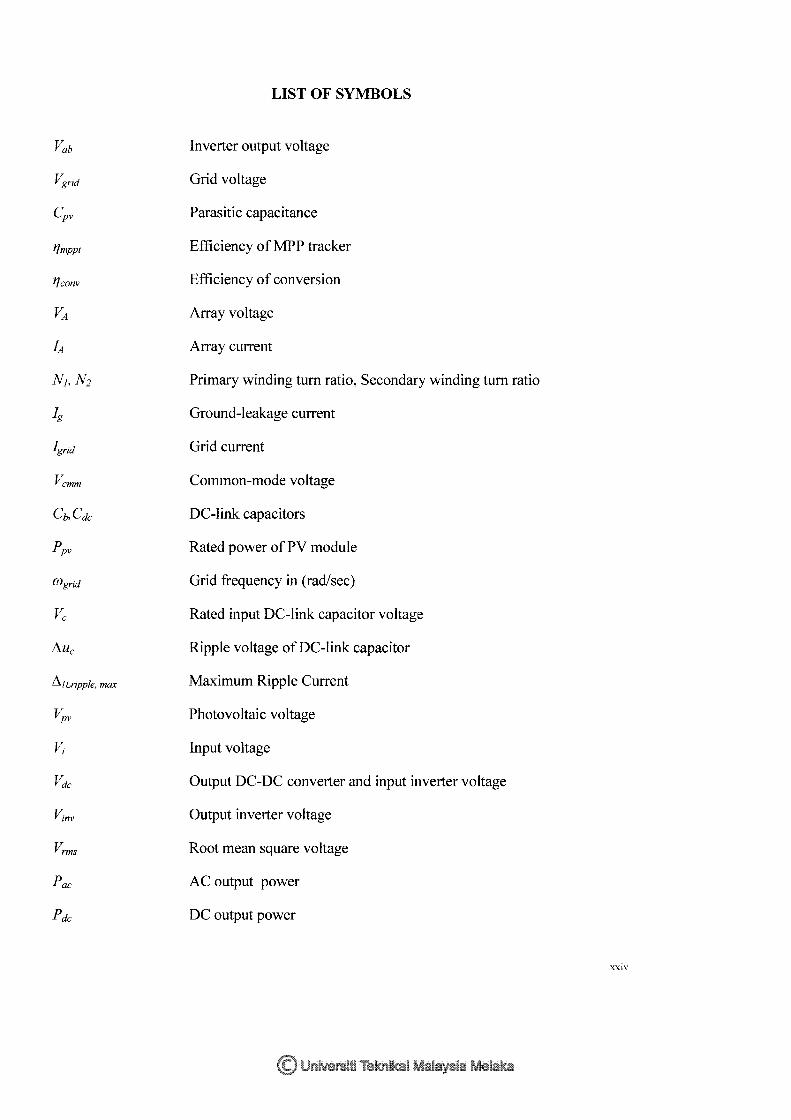
Vgrid
Cpv
1Jmppt
1Jconv
VA
J,4
N1,N2
lg
I grid
Wgrid
11nrtpple, max
Vpv
LIST OF SYMBOLS
Inverter output voltage
Grid voltage
Parasitic capacitance
Efficiency of MPP tracker
Efficiency of conversion
Array voltage
Array current
Primary winding tum ratio, Secondary winding tum ratio
Ground-leakage current
Grid current
Common-mode voltage
DC-link capacitors
Rated power of PV module
Grid frequency in (rad/sec)
Rated input DC-link capacitor voltage
Ripple voltage of DC-link capacitor
Maximum Ripple Current
Photovoltaic voltage
Input voltage
Output DC-DC converter and input inverter voltage
Output inverter voltage
Root mean square voltage
AC output power
DC output power
XXIV