Automatic Frequency Planning and Optimization Algorithm for ...
Optimization of Power MOSFET for High-Frequency
Synchronous Buck Converter
Yuming Bai
Dissertation submitted to the faculty of the
Virginia Polytechnic Institute and State University
in partial fulfillment of the requirements for the degree of
Doctor of Philosophy
in
Electrical Engineering
Alex Q. Huang, Chairman
Dong S. Ha
Guo Quan Lu
Jason S. Lai
Dusan Boroyevich
August 28, 2003
Blacksburg, Virginia
Keywords: Trench MOSFET, Buck converter, Optimization
Copyright 2003, Yuming bai

Optimization of MOSFET for High-frequency Synchronous Buck Converter
Yuming Bai
Dr. Alex Q. Huang, Chairman
Electrical and Computer Engineering
Abstract
Evolutions in microprocessor technology require the use of a high-frequency
synchronous buck converter (SBC) in order to achieve low cost, low profile, fast transient
response and high power density. However, high frequency also causes more power loss
on MOSFETs. Optimization of the MOSFETs plays an important role in the system
performance.
Circuit and device modeling is important in understanding the relationship between
the device parameters and the power loss. The gate-to-drain charge (Qgd) is studied by a
novel nonlinear model and compared with the simulation results. A new switching model
is developed, which takes into account the effect of parasitic inductance on the switching
process. Another model for dv/dt-induced false triggering-on relates the false-trigger-on
voltage with the parasitic elements of the device and the circuits.
Some techniques are proposed to reduce the simulation time of FEA in the circuit
simulation. Based on this approach, extensive simulations are performed to study the
switching performance of the MOSFET with the effect of the parasitic elements. Directed
by the analytical models and the experience acquired in the circuit simulation, the
MOSFET optimization is realized using FEA. Different optimization algorithms are
compared. The experimental results show that the optimized MOSFETs surpass the
mainstream commercialized products in both cost and performance.

Acknowledgement
I would like to express my sincere gratitude to my advisor, Dr. Alex Q. Huang, for his
guidance, support and encouragement during the entire course of my graduate study and
research at Virginia Polytechnic Institute and State University. His extensive knowledge
and creative thinking have been an invaluable help, without which none of this would
have been possible.
I gratefully thank Dr. Dusan Boroyevich, Dr. Jason S. Lai, Dr. Guo Guan Lu and Dr.
Dong S. Ha for their valuable contributions as members of my advisory committee.
I also thank the members of the Siliconix research and development group: Dr. Deva
Pattanayak, Dr. Kyle Terrill and Dr. King Owyang, for giving me the opportunity to gain
more experience in the industry.
I am indebted to all my fellow students at Virginia Power Electronics Center, now the
Center for power Electronics Systems. Their kindness has made my study in the Ph. D
program enjoyable. Especially, I thank Mr. Zhou Chen, Mr. Yin Liu, Mr. Zhenxue Xu,
Mr. Yu Meng, Mr. Yuhui Chen, Mr. Rengang Chen, Mr. Haifei Deng, Mr. Xin Zhang,
Mr. Xiaowu Sun, Mr. Xiaoming Duan and Mr. Bo Zhang for their friendship and help
with the experiments and simulations.
I am grateful to the CPES staff, Ms. Trish Rose, Ms. Teresa Shaw, Ms. Marianne
Hawthorne, Ms. Ann Craig, Mr. Steve Z. Chen, Mr. Mike King, for their assistance and
cooperation.
I thank my father, Fengsheng Bai, and my mother, Shuwen Yue, who brought me up
and encouraged my pursuit of higher knowledge.
III

Special thanks to my wife, Han Zhang, for her love during the past years. Her support
means everything.
IV

To my parents and wife
V

Contents
Abstract............................................................................................................................. II
Acknowledgement ...........................................................................................................III
Contents ...........................................................................................................................VI
List of Tables ................................................................................................................... IX
List of Figures................................................................................................................... X
Chapter 1 Introduction..................................................................................................... 1
1.1 Background .......................................................................................................... 1
1.2 Dissertation Outline ............................................................................................. 2
1.3 Simulation Tools .................................................................................................. 3
Chapter 2 Fundamentals of the Power MOSFET and Buck Converter...................... 5
2.1 Introduction to the Power MOSFET.................................................................... 5
2.1.1 Fundamentals of the Basic MOS Device ...................................................... 5
2.1.2 Structures of the Power MOSFET ................................................................ 6
2.1.3 Forward Blocking of the UMOSFET............................................................ 8
2.1.4 Specific On-resistance of the UMOSFET..................................................... 9
2.1.4.1 Specific Channel resistance.................................................................... 9
2.1.4.2 Specific resistance of drift region ........................................................ 10
2.1.4.3 Specific substrate resistance................................................................. 11
2.2 Introduction to the Buck Converter.................................................................... 16
2.2.1 Application Background in Personal Computers........................................ 16
2.2.2 Principle of the Buck Converter.................................................................. 17
2.2.3 Power Loss of the Buck Converter ............................................................. 22
Chapter 3 Analytical Modeling of the Buck Converter .............................................. 30
3.1 Modeling of the Power MOSFET in the Steady State ....................................... 30
3.2 Basic Switching Model of the High-side MOSFET in the Buck Converter ...... 32
3.2.1 Equivalent Circuit of the High-side MOSFET in the Buck Converter ....... 32
3.2.2 Switching Process of MOSFET with Inductive Load................................. 36
3.2.2.1 Turn-on process.................................................................................... 37
VI

3.2.2.2 Turn-off process ................................................................................... 38
3.3 Modeling Gate-to-Drain Capacitance (Cgd) and Charge (Qgd)........................... 42
3.3.1 Cgd and Qgd for the Non-Punch-Through Type of Depletion Region ......... 43
3.3.2 Cgd and Qgd for the Punch-Through Type of Depletion Region.................. 44
3.3.3 Analysis of the Switching Process With Non-Constant Cgd ....................... 50
3.3.4 Worked Examples of the Switching Process with Non-Constant Cgd and Qgd
................................................................................................................................... 54
3.4 A Novel Model for MOSFET Switching Loss Calculation ............................... 60
3.4.1 Analysis of the Turn-on Process ................................................................. 60
3.4.2 Analysis of the Turn-off Process ................................................................ 67
3.4.3 Worked Example of the Switching Process ................................................ 71
3.5 Analysis of dv/dt-Induced Spurious Turn-on of the MOSFET.......................... 73
Chapter 4 FEA Analysis of the Power Loss of the Buck Converter .......................... 83
4.1 Construction of the Buck Converter Using FEA ............................................... 84
4.1.1 Equivalent Circuit Used in the Simulation.................................................. 85
4.1.2 Estimation of the Parasitic Inductance........................................................ 87
4.2 Using FEA to Extract Spurious Turn-on Loss ................................................... 89
4.3 Automated Analysis of Power Loss................................................................... 94
4.3.1 Critical Timings in the Simulation.............................................................. 94
4.3.2 Expressions of the Power loss..................................................................... 96
4.3.3 Worked Example of the Program.............................................................. 100
4.4 Application of the FEA Simulator ................................................................... 104
4.4.1 Effect of the Design Parameters of the High-side MOSFET on Efficiency
................................................................................................................................. 105
4.4.2 Effect of the Design Parameters of the Low-side MOSFET on Efficiency
................................................................................................................................. 115
4.4.3 Effect of the Parasitic Inductance on Efficiency....................................... 121
4.5 Summary .......................................................................................................... 123
Chapter 5 Design of the Buck Converter Monolithically.......................................... 124
5.1 Introduction...................................................................................................... 124
5.2 Process Design ................................................................................................. 125
VII

VIII
TU5.2.1 Process FlowUT ............................................................................................. 125
TU5.2.2 Experimental Results and DiscussionUT ....................................................... 132
TU5.2.2.1 Voltage blocking capabilityUT ............................................................... 132
TU5.2.2.2 Performance of the MOSFETsUT........................................................... 133
TU5.3 Monolithic Design of the Buck ConverterUT ....................................................... 138
TU5.3.1 Design of the LDMOSUT .............................................................................. 138
TU5.3.2 Adaptive Deadtime Control of the Buck ConverterUT.................................. 139
TU5.3.3 Experimental Results and DiscussionUT ....................................................... 145
TUChapter 6 Optimization of the MOSFET for the Buck ConverterUT .......................... 151
TU6.1 PWM-Optimized Power MOSFETUT .................................................................. 151
TU6.2 Optimization Based on PWM Optimized Power MOSFETUT ............................ 156
TU6.2.1 Optimization Using Hooke-Jeeves Algorithm UT .......................................... 156
TU6.2.2 Optimization Using Decoupled Loops UT...................................................... 157
TU6.3 A Design Example and Experimental ResultsUT ................................................. 158
TU6.3.1 Design Background UT ................................................................................... 158
TU6.3.2 Design ProcedureUT ...................................................................................... 162
TU6.3.3 Experimental Results and DiscussionUT ....................................................... 162
TUChapter 7 Conclusions and Future WorkUT .................................................................. 166
TU7.1 Conclusions UT ...................................................................................................... 166
TU7.2 Summary of Research Contributions UT ............................................................... 167
TU7.3 Future Research DirectionsUT .............................................................................. 168
TUREFERENCES UT.............................................................................................................. 170
TUAppendix A Equivalence of UT
dVdQ
TU and UT
d
si
Wε
TU in the Calculation of Depletion Region
Capacitance UT ................................................................................................................... 179
TUVitaUT ................................................................................................................................. 181

List of Tables
Table 3.1 Calculation and simulation results of the example. .......................................... 55
Table 5.1 Comparison of the experimental and simulation results................................. 133
Table 6.1 A summary of the PWM-optimized MSOFET............................................... 155
IX

List of Figures
Fig. 2.1 Basic structure of an n-type MOSFET. ............................................................... 12
Fig. 2.2 Basic structure of LDMOS. ................................................................................. 12
Fig. 2.3 Structure of VMOSFET....................................................................................... 13
Fig. 2.4 Structure of DMOSFET....................................................................................... 13
Fig. 2.5 Structure of UMOSFET....................................................................................... 14
Fig. 2.6 Distribution of the electric field in the abrupt diode under different breakdown
conditions.................................................................................................................. 14
Fig. 2.7 Current flowline in UMOSFET........................................................................... 15
Fig. 2.8 Specific resistance of the drift region. ................................................................. 15
Fig. 2.9 Basic topology of the buck converter. ................................................................. 16
Fig. 2.10 Waveform of the output voltage (Vsw). ............................................................. 26
Fig. 2.11 Equivalent circuit of the conventional buck converter. ..................................... 26
Fig. 2.12 Equivalent circuit of the synchronous buck converter. ..................................... 27
Fig. 2.13 Operating sequence of the synchronous buck converter (Part I)....................... 27
Fig. 2.14 Operating sequence of the synchronous buck converter (Part II). .................... 28
Fig. 2.15 Simplified switching waveforms of the high-side MOSFET. ........................... 28
Fig. 2.16 Circuit used in the efficiency measurement. ..................................................... 29
Fig. 3.1 The equivalent circuit of the power MOSFET. ................................................... 33
Fig. 3.2 Equivalent circuit of the high-side MOSFET...................................................... 34
Fig. 3.3 Equivalent circuit of the high-side MOSFET...................................................... 34
Fig. 3.4 Equivalent circuit of the high-side MOSFET...................................................... 35
Fig. 3.5 Equivalent circuit of the high-side MOSFET...................................................... 35
Fig. 3.6 Equivalent circuit of the high-side MOSFET with constant current source as gate
driver. ........................................................................................................................ 36
Fig. 3.7 Waveform of Vgs in the turn-on process of the MOSFET................................... 39
Fig. 3.8 Waveform of Id and Vds in the turn-on process of the MOSFET. ....................... 40
Fig. 3.9 Waveform of the power loss in the turn-on process of the MOSFET................. 40
Fig. 3.10 Waveform of Vgs in the turn-off process of the MOSFET ................................ 41
Fig. 3.11 Waveform of Id and Vds in the turn-off process of the MOSFET...................... 41
Fig. 3.12 Waveform of the power loss in the turn-off process of the MOSFET. ............. 42
X

Fig. 3.13 One dimensional model of Cgd in the UMOSFET. .......................................... 47
Fig. 3.14 Distribution of the electric field in the non-punch-through type of depletion
region. ....................................................................................................................... 47
Fig. 3.15 Distribution of the electric field in the punch-through type of depletion region.
................................................................................................................................... 48
Fig. 3.16 Comparison of calculated and simulated Cgd. ................................................... 48
Fig. 3.17 One-dimensional modeling of Cgd. .................................................................... 49
Fig. 3.18 One-dimensional modeling of Qgd0. .................................................................. 49
Fig. 3.19 Simulated turn-on waveforms. .......................................................................... 50
Fig. 3.20 Comparison of the simulation and calculation results....................................... 56
Fig. 3.21 Effect of the punch-through on the turn-on loss................................................ 57
Fig. 3.22 Effect of the punch-through on the turn-on loss................................................ 57
Fig. 3.23 Effect of the doping concentration on the turn-on loss. .................................... 58
Fig. 3.24 Effect of the Doping concentration on the turn-on loss..................................... 58
Fig. 3.25 Effect of the thickness of the gate oxide on the turn-on loss............................. 59
Fig. 3.26 Effect of the thickness of the gate oxide on the turn-on loss............................. 59
Fig. 3.27 General switching waveforms. .......................................................................... 65
Fig. 3.28 Equivalent circuit of turn-on process................................................................. 65
Fig. 3.29 Equivalent circuit of turn-on process................................................................. 66
Fig. 3.30 Equivalent circuit of turn-on process................................................................. 66
Fig. 3.31 Equivalent circuit of turn-on process................................................................. 67
Fig. 3.32 Equivalent circuit of turn-off process. ............................................................... 70
Fig. 3.33 Equivalent circuit of turn-off process. ............................................................... 70
Fig. 3.34 Equivalent circuit of turn-off process. ............................................................... 71
Fig. 3.35 Equivalent circuit of turn-off process. ............................................................... 71
Fig. 3.36 Effect of Ls on the switching loss (Ld = 0.8 nH). .............................................. 72
Fig. 3.37 Effect of Ld on the switching loss (Ls = 1.2 nH). .............................................. 73
Fig. 3.38 Equivalent circuit of power MOSFET for dv/dt-induced spurious turn-on
analysis...................................................................................................................... 77
Fig. 3.39 Equivalent circuit of power MOSFET for dv/dt induced spurious urn-on
analysis...................................................................................................................... 78
XI

Fig. 3.40 Equivalent circuit of power MOSFET for dv/dt induced spurious urn-on
analysis...................................................................................................................... 78
Fig. 3.41 Equivalent Circuit of Power MOSFET for dv/dt induced spurious urn-on
Analysis..................................................................................................................... 79
Fig. 3.42 Circuit considering the Igd effect. ...................................................................... 79
Fig. 3.43 Circuit considering the Vgss effect. .................................................................... 80
Fig. 3.44 An example of the analytical results.................................................................. 80
Fig. 3.45 Comparison of Vmax between the new and old models...................................... 81
Fig. 3.46 Comparison between analytical and simulation results..................................... 81
Fig. 3.47 Effect of the active area on the spurious turn-on voltage. ................................. 82
Fig. 4.1 General circuit of the buck converter. ................................................................. 84
Fig. 4.2 Equivalent circuit of the driver in the buck converter. ........................................ 84
Fig. 4.3 Circuit used in the mixed-mode simulation......................................................... 85
Fig. 4.4 Simulated Vds and Vgs of the low-side MOSFET.............................................. 91
Fig. 4.5 Calculated inductance of a single wire. ............................................................... 91
Fig. 4.6 Calculated inductance of the metal strip.............................................................. 92
Fig. 4.7 Simulated inductance of the metal strip. ............................................................. 92
Fig. 4.8 Current through the source of the low-side MOSFET without spurious turn-on.93
Fig. 4.9 Current through the source of the low-side MOSFET with spurious turn-on. .... 93
Fig. 4.10 An example of the power analysis result......................................................... 104
Fig. 4.11 Effects of trench width on the Qsw, Rds and FOM. .......................................... 108
Fig. 4.12 Effect of trench width on efficiency. ............................................................... 109
Fig. 4.13 Effects of mesa width on Qsw, Rds and FOM................................................... 109
Fig. 4.14 Effect of mesa width on efficiency.................................................................. 110
Fig. 4.15 Effects of the gate oxide thickness on Qgd, Rds and FOM. .............................. 110
Fig. 4.16 Effect of the gate oxide thickness on efficiency.............................................. 111
Fig. 4.17 Effects of Ovp on Qgd, Rds and FOM............................................................... 111
Fig. 4.18 Effect of Ovp on efficiency. ............................................................................ 112
Fig. 4.19 Effects of the doping concentration of the drift region on Qgd, Rds and FOM. 112
Fig. 4.20 Effect of the doping concentration of the drift region on the efficiency. ........ 113
XII

Fig. 4.21 Effect of the breakdown voltage (BV) on efficiency. ..................................... 113
Fig. 4.22 Turn-off waveforms of the high-side MOSFET.............................................. 114
Fig. 4.23 Effect of Vt on efficiency. ............................................................................... 114
Fig. 4.24 Effect of trench width on efficiency. ............................................................... 117
Fig. 4.25 Effect of mesa width on efficiency.................................................................. 118
Fig. 4.26 Effect of the gate oxide thickness on efficiency.............................................. 118
Fig. 4.27 Effect of Ovp on efficiency. ............................................................................ 119
Fig. 4.28 Effect of the doping concentration of the drift region on efficiency. .............. 119
Fig. 4.29 Effect of the breakdown voltage (BV) on efficiency. ..................................... 120
Fig. 4.30 Effect of Vt on efficiency. ............................................................................... 120
Fig. 4.31 Effect of Ldhi on efficiency. ............................................................................. 121
Fig. 4.32 Effect of Ldhi on Vdshimax. ................................................................................. 122
Fig. 4.33 Effect of Lshi on efficiency............................................................................... 122
Fig. 4.34 Effect of the area of the high-side MOSFET on the switching loss of the high-
side MOSFEF.......................................................................................................... 123
Fig. 5.1 Topology of monolithically integrated buck converter. .................................... 128
Fig. 5.2 Isolation and signal flow in the monolithically integrated buck converter. ...... 128
Fig. 5.3 Simulated cross section of the process flow (Step 4). ....................................... 129
Fig. 5.4 Simulated cross section of the process flow (Step 6). ....................................... 129
Fig. 5.5 Simulated cross section of the process flow (Step 8). ....................................... 129
Fig. 5.6 Simulated cross section of the process flow (Step 9). ....................................... 130
Fig. 5.7 Simulated cross section of the process flow (Step 11). ..................................... 130
Fig. 5.8 Simulated cross section of the process flow (Step 12). ..................................... 130
Fig. 5.9 Simulated cross section of the process flow (Step 13). ..................................... 131
Fig. 5.10 Simulated cross section of the process flow (Step 14). ................................... 131
Fig. 5.11 Simulated cross section of the process flow (Step 15). ................................... 131
Fig. 5.12 Simulated cross section of the process flow (Step 16). ................................... 132
Fig. 5.13 Simulated cross section of the process flow (Step 17). ................................... 132
Fig. 5.14 Pictures of the fabricated device structure....................................................... 134
Fig. 5.15 Experiment results of the breakdown characteristic between the P-well and N-
well.......................................................................................................................... 135
XIII

Fig. 5.16 Experiment results of the breakdown characteristic between the P-body and N-
well.......................................................................................................................... 135
Fig. 5.17 Experiment results of the forward conduction characteristic of the low-voltage
NMOS. .................................................................................................................... 136
Fig. 5.18 Experiment results of the forward conduction characteristic of the low-voltage
PMOS...................................................................................................................... 136
Fig. 5.19 Experiment results of the forward conduction characteristic of the LDMOS. 137
Fig. 5.20 DC transfer characteristic of the inverter. ....................................................... 137
Fig. 5.21 Layout of the power LDMOS.......................................................................... 143
Fig. 5.22 Optimization of the device area....................................................................... 143
Fig. 5.23 Function diagram of the design ...................................................................... 144
Fig. 5.24 Using the parasitic NPN transistor as the voltage sensor ................................ 144
Fig. 5.25 Using the LDMOS and a low voltage MOSFET as the voltage sensor .......... 145
Fig. 5.26 Layout of the design ........................................................................................ 146
Fig. 5.27 Die in the SOIC20 ceramic frame ................................................................... 146
Fig. 5.28 Circuit for the efficiency measurement ........................................................... 147
Fig. 5.29 Measured efficiency Vin=12V @1MHz ......................................................... 147
Fig. 5.30 Switching waveforms of the low-side MOSFET ............................................ 148
Fig. 5.31 Switching waveforms of the high-side MOSFET ........................................... 148
Fig. 5.32 Leakage power loss ......................................................................................... 149
Fig. 5.33 Efficiency without the leakage power ............................................................. 149
Fig. 5.34 Experimental results of the adaptive deadtime control ................................... 150
Fig. 6.1 General optimization procedure ........................................................................ 160
Fig. 6.2 An optimization example using Hooke-Jeeves algorithm................................. 160
Fig. 6.3 Optimization using decoupled method.............................................................. 161
Fig. 6.4 An optimization example using decoupled method .......................................... 161
Fig. 6.5 Simulated efficiency of the design. ................................................................... 164
Fig. 6.6 Comparison of the measured and simulated efficiency at full load. ................. 164
Fig. 6.7 Comparison of the efficiency and device area................................................... 165
XIV

Chapter 1 Introduction
1.1 Background
The most important factors in achieving higher speed and greater complexity for the
microprocessor are the reduction of the minimum device feature size and the increase of
the components per chip [E1]. Such advanced processors require lower supply voltages
and produce large, fast changes in the current they draw, which in turn demands special
power supplies to provide lower voltages with higher current capabilities [D1]-[D5].
There are several topology candidates for such power supply [D6]-[D9]. The most widely
used in the industry is the multi-phase Synchronous Buck Converter (SBC), because it is
simpler and more cost effective.
The large dynamic loads with high current slew rates, which occur when the system
switches from the active mode to the sleep mode and vice versa, make the parasitic
impedance of the power supply connection to the load have a dramatic effect on the
power supply voltage. In order to minimize the effects of the interconnection parasitics,
today’s power supply must be a point-of-load on-board power supply, which is powered
up from the existing voltages available in the system and is required to have high power
densities because the space of the power supply on the motherboard is very limited
[D10]-[D11].
The high operating frequency of the power supply can achieve high power density and
fast transient response [D12]-[D16]. However, the power loss on the semiconductor
device also increases with the frequency. Such loss is converted into heat thereby causing
the temperature to rise, which reduces the system reliability and can even kill the device
if the temperature is too high [E2]. Indeed, it is the performance of the semiconductor
device that determines the upper limit of the operating frequency of the power supply.
Because it is impractical to adequately cool the converter elements on the motherboard,
1

the key solution for reducing the loss on the semiconductor device relies on the device
technology itself.
From the device standpoint, both the power bipolar transistor and the metal-oxide-
semiconductor field-effect-transistor (MOSFET) can be used in the power supply.
However, studies show that the MOSFET is a better choice than the bipolar transistor for
such applications. First of all, the power MOSFET is a voltage-controlled device. The
high input impedance of the MOSFET makes its gate drive circuitry much simpler than
that of bipolar transistor. For a short duration, power MOSFETs can withstand the
simultaneous application of high voltage and current without undergoing fatal failure for
a short duration. Further, the MOSFETs can be easily paralleled because their on-
resistance increases with increasing temperature.
Another power device candidate for VRM application is the junction field-effect
transistor (JFET). In order to achieve low on-resistance, the JFET is a device that is
normally on or operating in depletion mode, which means that a positive voltage must be
applied on the gate terminal to turn the device off. This is the main drawback of the
JFET, because it requires a more complex drive circuit, which is not compatible with the
prevailing system.
1.2 Dissertation Outline
This dissertation is devoted to the optimization of the power MOSFET for use in the
high-frequency DC-DC converter. Because there are many device parameters related to
the optimization, a good qualitative insight into the device performance in the circuit is
indispensable in understanding and simplifying the optimization process. Therefore,
several analytical models are developed and presented before the introduction of the
Finite Element Analysis FEA method. The dissertation is arranged as follows.
2

There are seven chapters including an introduction. Chapter 2 describes the
background information about the power MOSFET and DC-DC buck converter.
Chapter 3 presents three analytical models regarding the switching performance of the
trench MOSFET.
Chapter 4 investigates the performance of the MOSFET in the buck converter using
FEA. An approach for extracting a detailed loss breakdown of the MOSFET is proposed.
Analysis of the effect of the parasitic components on the loss is performed.
Chapter 5 proposes an economical Integrated Circuit (IC) process for the monolithic
integration of the buck converter. In addition, a monolithic design is presented.
Chapter 6 discusses the automated optimization procedures. Experimental results are
presented to verify the optimization concept.
Finally, conclusions of this work and suggestions for future work are outlined in
Chapter 7.
1.3 Simulation Tools
In this dissertation, the FEA models of the device are constructed and calculated by
commercial software. Because a lot of results presented in this dissertation are based on
simulations, it is necessary to provide a brief description of the Technology Computer
Aided-Design (TCAD) tools from Avant! Corporation. The TCAD has three main
functions: device simulation, process simulation and visualization.
1) The program mediciTM [E3] simulates the electrical behavior of semiconductor
devices by solving the following basic Equations.
Poisson's Equation:
3

4
),,( zyxD ρ=∇r
, (1.1)
where Dr
is the displacement vector and ),,( zyxρ is the total electric charge density.
Continuity Equations:
nnn Jq
UGtn r
∇⋅+−=∂∂ 1 , (1.2)
and ppp Jq
UGtp r
∇⋅+−=∂∂ 1 , (1.3)
where n is the electron density, p is the hole density, nJr
is the electron current density,
pJr
is the hole current density, and GBn B (UBn B) and GBp B (UBpB) are the electron and hole
generation (recombination) rates respectively.
Current-Density Equations:
nqDEnqJ nnn ∇+=rr
µ , (1.4)
and pqDEpqJ ppp ∇−=rr
µ , (1.5)
where µBnB is the electron mobility, µBp B is the hole mobility, and DBn B and DBp B are diffusion
constants of the electron and the hole respectively.
2) The program tsuprem4P
TMP [E4] is a very powerful two-dimensional simulator for
simulating the process steps employed in the fabrication of silicon devices. The major
process steps include epitaxial growth, diffusion, oxidation, ion implantation, deposition,
metallization and etching. The output information generated by the simulator includes
boundaries of various materials in the structure and the impurity distributions of each
material. Such information can be fed into the device simulator mediciP
TMP to evaluate the
electrical performance of the device.
3) The program tv2dP
TMP is the visualization tool for simulations. It can plot the cross-
section of the device structure, showing the doping profile, electron and hole densities,
electric field, current flowline, etc., as required. Moreover, tv2dP
TMP can display either the
current and voltage waveforms generated by the device or a mixed-mode circuit
simulation performed using mediciP
TMP.

5
Chapter 2 Fundamentals of the Power MOSFET and Buck Converter
2.1 Introduction to the Power MOSFET
2.1.1 Fundamentals of the Basic MOS Device
The basic structure of an n-type MOSFET [E5] [E6] is shown in Fig. 2.1, where nP
+P
represents heavily doped (low resistivity) n-type silicon. The difference between the
source and drain is that the source nP
+P is shorted to the P-substrate by the source metal.
This is important for fixing the potential of the P-substrate for normal device operation.
For power applications, the MOSFET is required to be off when the voltage on the gate is
0. The turn-on of the MOSFET relies on the formation of a conductive layer on the
surface of the semiconductor, when a positive (negative) voltage is applied on the gate of
the n (p) type MOSFET. For the n-type MOSFET, as VBg B increases, electrons flow to the
interface between the oxide and silicon, and a charge layer is formed to provide a
"channel" for the current. When this phenomenon occurs, the value of VBg B is called the
threshold voltage (VBthB). In semiconductor physics, the threshold voltage is defined as the
applied gate voltage required to make the surface of the silicon as much n-type as the
substrate is p-type. The threshold voltage can be written as
msox
ssdepfpth C
QQV φφ +
−+= 2 , (2.1)
where i
afp n
Nq
kT ln=φ , (2.2)
afpsidep NqQ φε4= , (2.3)
ox
oxox T
C ε= . (2.4)
The definitions of the other symbols are:
1) k is the Boltzmann's constant: k=1.38×10P
-23P J/K,
2) T is the absolute temperature,
3) q is the electronic charge: q=1.60×10P
-19P C,
4) NBaB is the acceptor doping concentration of the substrate,

6
5) NBi B is the intrinsic carrier concentration of the silicon,
6) εBsi B is the dielectric constant of silicon: εBsi B=1.03×10P
-12P F/cm,
7) QBss B is the fixed charge located in the oxide close to the oxide-silicon interface,
8) εBox B is the dielectric constant of oxide: εBoxB=3.45×10P
-12P F/cm, and
9) TBoxB is the thickness of the gate oxide.
The resistance from drain to source of the MOSFET is determined by the property of
the charge layer in the channel, and can be expressed as
)( thgsoxnchg
oxgch VVW
TLR
−=
εµ, (2.5)
where µBnch B is the mobility of the electron in the channel. The definition of LBg B (channel
length) and WBg B (channel width) are shown in Fig. 2.1.
2.1.2 Structures of the Power MOSFET
The basic structure shown in Fig. 2.1 is not suitable for high-voltage applications,
because in order to achieve low resistance expressed in Equation (2.5), shorted channel
length (LBg B) and thinner gate oxide (TBox B) are required. However, both LBg B and TBox B are
related to the breakdown voltage of the MOSFET. If LBg B is too small, the junction
breakdown or punch-through of NP
+PPNP
+P will occur; if TBoxB is too thin, the oxide directly
adjacent to the drain can be destroyed by the electric field. To alleviate the effect of the
electrical filed on the gate oxide for high-voltage applications, the following structures
have been developed [E7].
1) Lateral Diffusion MOSFET (LDMOS)
Compared to the structure of the basic MOSFET, LDMOS [A16]-[A18](Fig. 2.2) has
an additional lightly doped (nP
-P) region between the oxide and the drain. Because most of
the voltage applied on the drain is supported by the nP
-P drift region, the LDMOS can
withstand high voltage with thinner gate oxide and shorter channel length. However, like
the basic MOSFET, the current of the LDMOS still flows on the surface of the silicon,
the utility of the silicon is low, and the specific resistance (resistance per area) is

relatively high. In vertical power MOSFETs, the n- drift region is located inside the
silicon. Therefore, a cross-section of the current path is enlarged without sacrificing the
silicon area.
2) Power VMOSFET (Fig. 2.3)
The name VMOSFET is derived from the V-shaped groove along which current flows.
Although the VMOSFET was the first commercialized structure of the power MOSFET,
it was replaced by the Double-diffusion MOSFET (DMOSFET) because of the high
electrical1 field at the tip of the V-groove.
3) Power DMOSFET (Fig. 2.4)
When Vg is higher than the threshold voltage and Vds is positive, the electron current
of the MOSFET travels horizontally through the channel and then vertically to the drain.
A more direct, shorter current path can be achieved if the channel is orientated vertically
instead of along the silicon surface. This idea is realized by the structure of the
UMOSFET.
4) Power UMOSFET (Fig. 2.5)
Like the VMOSFET, the name UMOSFET is also derived from the U-shaped groove
formed in the gate region. Compared to the DMOSFET, the UMOSFET [A1]-[A5] has
no JFET region and has higher channel density to significantly reduce the on-resistance
of the device. Moreover, the UMOSFET has no sharp oxide tip (as exists in the
VMOSFET), because the corners of the gate oxide located in the n-drift region can be
rounded by isotropic etching. In order to prevent the catastrophic destruction of the gate
oxide due to the electrical crowding at the corner of the trench, the P-body is usually
designed to be deep enough and the doping concentration at the bottom of the P-body is
high enough to ensure that the voltage breakdown occurs first at the junction of the P-
body and in the N- drift region. Therefore, the voltage can be clamped to save the gate
oxide. In the rest of this dissertation, the discussion will focus on the UMOSFET. The
important electrical performances of the UMOSFET [C1]-[C4] are reviewed in the next
two sections.
7

8
2.1.3 Forward Blocking of the UMOSFET
Before the discussion of the forward blocking of the UMOSFET, the basic theory of
diode breakdown must be reviewed to provide some background information.
For an ideal parallel-plane diode, the dominant breakdown mechanism is the impact
ionization effect. Because the ionization coefficients strongly depend on the electric field,
the diode breakdown occurs when a high electric field exists inside the structure. The
maximum electric field is usually called the critical electric field and is given by
8/14010NEc = , (2.6)
where N is the doping concentration of the lightly doped silicon.
Ignoring the build-in potential for abrupt junction, the maximum electric field can be
related to the applied voltage by
si
mqNVEε
2= . (2.7)
By substituting the critical electric field Equation (2.6) into Equation (2.7), the
breakdown voltage is found to be
4/3131034.5 −×= NBV . (2.8)
Then, the maximum depletion length at the point of breakdown is
8/710max 1067.2 −×= NL . (2.9)
If the total length of the drift region is less than LBmax B, the punch-through will occur as
shown in Fig. 2.6, and the breakdown voltage is given by
si
nnc
qNLLEBVε2
2
−= . (2.10)
For a given breakdown voltage, Equation (2.10) shows that there are many
combinations of the depletion length L Bn B and the doping concentration N. The root of LBn B in
Equation (2.10) is

9
qN
BVqNEEL sicsicsi
n
⋅−−=
εεε 222
. (2.11)
Considering EBcB as a function of N (2.6), (2.11) can be rewritten as
qN
BVqNNNL sisisi
n
⋅−×−=
εεε 2106.14010 4/1278/1
. (2.12)
In principle, the UMOSFET can be designed as a punch-through-type device as long
as the doping concentration of the drift region is less than
3/4
13max 1034.5
−
⎟⎠⎞
⎜⎝⎛
×=
BVN , (2.13)
which is derived from Equation (2.8).
As mentioned in section 2.1.1, because the bottom of the P-body is heavily doped, the
breakdown voltage of the UMOSFET is determined by the abrupt junction of the P-body
and the NP
-P drift region. When a positive voltage is applied to the drain of the UMOSFET,
the voltage is mainly supported by the depletion layer of the drift region.
2.1.4 Specific On-resistance of the UMOSFET
The specific on-resistance of the UMOSFET is the resistance per unit area between the
drain and source terminal in the on state. The simulated current flow of the UMOSFET is
shown in Fig. 2.7. The main resistance components of the UMOSFET are the channel,
the drift region and the substrate.
2.1.4.1 Specific Channel resistance
The definition of the UMOSFET’s channel resistance is the same as that of the basic
MOSFET. Therefore, the specific channel resistance can be derived from Equation (2.5),
as follows:

10
)(2
)(
thgsoxnch
oxgtmspch VVT
LWWR
−
+=
µε
, (2.14)
where WBmB and WBt B are the width of mesa and trench, respectively (Fig. 2.6).
2.1.4.2 Specific resistance of drift region
As shown in Fig. 2.6, because the current spreads from the channel into the drift
region, the drift region resistance is not directly proportional to LBn B or 1/WBmB. If we assume
that the current-spreading angle is 45 degree, a reasonably accurate model can be
expressed as
)]2
(ln2
[1 mn
t
tmtm
ndft
WL
WWWWW
qNR −+
++=
µ, (2.15)
where Cq 19106.1 −×= is the electronic charge, nµ is the electron mobility of silicon in
the NP
-P drift region (the typical value of nµ is 1350 cmP
2P/V.s), and N is the doping
concentration in the NP
-P drift region.
There are two sections in Equation (2.15). The first is contributed by the current
spreading at a 45-degree angle; the second is associated with the drift region, the cross-
section of which is equal to the pitch. As discussed in section 2.1.2, the length of the drift
region LBnB is a function of the breakdown voltage BV and the doping concentration N, as
shown in Equation (2.12). Substitution of (2.12) into (2.15) yields
]2
2106.14010ln
2[1 4/1278/1
msisisi
t
tmtm
ndft
WqN
BVqNNNW
WWWWqN
R −⋅−×−
+++
=εεε
µ. (2.16)
The relationship between the doping concentration and the specific resistance of the
drift region is illustrated in Fig. 2.8. The calculation shows that the punch-through type of
power UMOSFET has a higher resistance than that of the non-punch-through power
MOSFET.

11
2.1.4.3 Specific substrate resistance
The contribution to the specific resistance arising from the current through the heavily
doped substrate is simply equal to
sbsbspsb LR ρ= , (2.17)
where ρ BsbB is the resistivity of the substrate. The typical values of ρ Bsb Band LBsb B are 2 mΩ.cm
and 200 µm. For a low voltage, high-density UMOSFET, substrate resistance can be
more than 20% of the total resistance.
In reality, the package resistance [C22]-[C27] is another important component. The
typical value of a state-of-the-art package like LFPAK is about 0.8 mΩ. Currently, the
synchronous MOSFET (low-side MOSFET) in the synchronous buck converter is lower
than 4 mΩ [A8]-[A15]. This means that the package resistance is not negligible in terms
of on-resistance or power loss.

N+
P-substrate
N+
Wg
LgP+
polysilicon
oxide
gate
drainsource
N+
P-substrate
N+
Wg
LgP+
polysilicon
oxide
gate
drainsource
Fig. 2.1 Basic structure of an n-type MOSFET.
N+
P-substrate
N+
Wg
LgP+
polysilicon
oxide
gate drain
source
N- drift region N+
P-substrate
N+
Wg
LgP+
polysilicon
oxide
gate drain
source
N- drift region
Fig. 2.2 Basic structure of LDMOS.
12

Gate
N+
N- drift region
oxide
N+
P-bodyP-bodyN+
source source
drain
Gate
N+
N- drift region
oxide
N+
P-bodyP-bodyN+
source source
drain
Fig. 2.3 Structure of VMOSFET.
N+
N- drift region
oxidesource
N+
P-bodyN+
P-body
sourcegate
drain
N+
N- drift region
oxidesource
N+
P-bodyN+
P-bodyN+
P-bodyN+
P-body
sourcegate
drain
Fig. 2.4 Structure of DMOSFET.
13

14
Gate
N+
N- drift region
Gate oxide
P-body
source
drain
N+N+ N+N+
Trenchsource source
mesa Gate
N+
N- drift region
Gate oxide
P-body
source
drain
N+N+ N+N+N+N+ N+N+ N+N+N+N+
Trenchsource source
mesa
Fig. 2.5 Structure of UMOSFET.
P+ N drift region N+
Ln
Ec
Lmax
P+ N drift region N+
Ln
Ec
Lmax
Non-punch through punch through
P+ N drift region N+
Ln
Ec
Lmax
P+ N drift region N+
Ln
Ec
Lmax
Non-punch through punch through Fig. 2.6 Distribution of the electric field in the abrupt diode under different breakdown
conditions.

15
source
drain
Gate
N+
N- drift region
P-body
N+
Wm/2 Wt/2
Ln
Lsb
source
drain
Gate
N+
N- drift region
P-body
N+
Wm/2 Wt/2
Ln
Lsb
Fig. 2.7 Current flowline in UMOSFET.
0
0.2
0.4
0.6
0.8
1
1.2
1.E+15 1.E+16 1.E+17
Doping concentration
Spec
ific
resi
stan
ce o
f the
drif
t reg
ion
(moh
m.c
m2 )
BV=20BV=30BV=40
Fig. 2.8 Specific resistance of the drift region.

gnd
VoutL
CR
Vin +
-
a
bVsw
gnd
VoutL
CR
Vin +
-
a
bVsw
Fig. 2.9 Basic topology of the buck converter.
2.2 Introduction to the Buck Converter
2.2.1 Application Background in Personal Computers
The basic function of the DC-DC converter is to change the DC input voltage to
another DC output voltage. Depending on the application, the input voltage can be lower
(buck converter) or higher (boost converter) than the input voltage. In personal computers
(PCs), the value of the output voltage is determined by the supply voltage needed by the
microprocessor. Currently, the prevailing voltage is about 1.3 V. The input voltage of the
converter is determined by the supply voltages that already exist in the system and which
are used for powering other parts of the system. Today's PC employs a hybrid power
system. Because the 5V output of the silver box must supply power to the memory chips
and other peripherals, it cannot provide sufficient power for the high-power
microprocessor. In the desktop, the DC-DC converter is powered up from a 12V voltage
source, which is also shared by the disk drives. In the notebook, the DC-DC converter is
16

17
powered up by the batteries or the output of the AC-DC adaptor. Because the voltage of
the batteries varies with the utility time, the output of the batteries ranges from 9 V to 12
V. The output of the AC-DC adaptor is 20 V. Such high voltage levels are required to
charge the battery.
In both desktops and notebooks, the input voltage of the DC-DC converter is higher
than the output voltage. Therefore, the buck converter is widely used in the PC. The basic
properties of the buck converter are reviewed in the next section.
2.2.2 Principle of the Buck Converter
Fig. 2.9 illustrates the topology of the buck converter. It consists of an input voltage
source, a single-pole double-throw switch, a low-path LC filter and a load represented by
a resistor R.
When the switch is in position a, the switch output voltage VBs B is equal to the converter
input voltage VBin B; when the switch is in position b, VBs B is equal to zero. The switch
position is varied periodically, as illustrated in Fig. 2.10; therefore VBs B is a rectangular
waveform having frequency FBs B and period TBs B=1/FBs B. The duty cycle D is defined as the
fraction of time in which the switch occupies position a.
Because the DC component of a periodic waveform is equal to its average value, the
DC component of VBs B is
ins VDV ×= . (2.18)
In addition to the DC component, the voltage waveform of the switch output also
contains harmonics of the switching frequency. In the applications for the DC-DC
converter, these harmonics must be removed, such that the output voltage is essentially
equal to the DC component. A low-pass LC filter can be employed for this purpose. The
average voltage of VBout B is equal to the average voltage of VBs B. Otherwise, the current
through inductor L will be infinite. This is called the principle of inductor volt-second
balance: in steady state, the net volt-seconds applied on an inductor must be zero.

In practice, the switch is realized using a MOSFET and diodes, which are controlled
by IC drivers, as shown in Fig. 2.11 and Fig. 2.12. Usually, the output stage of the driver
is a CMOS buffer, which has two states (low and high). When the output of the buffer is
low, the output is connected to the ground by an NMOSFET, which is fully on.
Therefore, the output voltage level is zero, and the power MOSFETs driven by the buffer
are off, because the threshold voltage of the power MOSFET is typically between 1 V
and 3 V. When the output of the buffer is high, the output is connected to the supply of
the IC driver by a PMOSFET, which is fully on. Hence, the output voltage level is equal
to the supply voltage, the typical value of which is 5V in a notebook or 12V in a desktop,
and the power MOSFETs driven by the buffer are on, because both 5 V and 12 V are
higher than the threshold voltage of the power MOSFETs.
Although the circuit of the conventional buck converter is simpler than that of the
synchronous one, the former is not used for the PC application. The reason is that the
operation current at full load is about 10 A. Assuming the voltage drop on the low-side
diode is 0.7 V, then the power loss on the diode will be 7 W. Such high temperature
cannot be alleviated without an expensive cooling system.
In reality, in order to handle larger levels of output current, a multi-channel setup is
usually employed, and each channel contains more than one device in parallel in order to
share the current and the power loss in discrete applications.
As shown in Fig. 2.13 and Fig. 2.14, the steady state operation of the synchronous
buck converter consists of the following stages.
1) From t0 to t1, the output of the low-side driver is high and the output of the high side
driver is low. There is no current flowing through either the high-side MOSFET or the
voltage source Vin, because the high-side MOSFET is off. Assuming the filter capacitor is
large enough that the variation of the output voltage Vout can be ignored, then the output
current of the buck converter, i.e. the current through the resistor R is
18

19
R
VI outout = . (2.19)
With the assumption that output voltage VBoutB is much larger than the absolute voltage at
node sw (VBswB), the voltage on inductor L can be considered to be equal to VBout B. Therefore,
the current variation with the time of the inductor L is
L
VdtdiK outL ==1 . (2.20)
Considering that the DC current through the capacitor C must be zero, the output current
should be equal to the DC current of inductor L. So, the total current through the inductor
L is a function of time t, such that
0101
00101 2
)(2)( IT
ttTIti outL ∆−−
+= , (2.21)
where TB01B is the during of this duration
0101 TTT −= , (2.22)
and ∆I B01B is the current ripple of inductor L during TB01B, as follows:
0101101 TL
VTKI out==∆ . (2.23)
Based on Equation (2.21), we know that the current through the inductor at the beginning
(t=tB0B) and the end (t=tB1 B) of this operating period are
2
)( 01001
IIti outL∆
+= , (2.24)
and 2
)( 01101
IIti outL∆
−= , (2.25)
respectively.
Since the high-side MOSFET is off, the current through the inductor is equal to the
current though the low-side MOSFET. The current direction of the low-side MOSFET is
from the source to the drain, and the voltage at node sw is
dsloLsw RtitV ×−= )()( , (2.26)
where RBdsloB is the on-resistance of the low-side MOSFET.

20
In order to get some idea of the practical values of the variables addressed above, it is
helpful do some simple calculations based on commercial MOSFETs and inductors. For
an example using an operation frequency (FBs B) of 500 KHz, an input voltage (VBin B) of 12 V
and an output voltage (VBout B) of 1.3 V, using Equation (2.18), we know the duration of this
period is about
sFV
VTDTsin
outs µ78.11)1()1(01 =−=−= . (2.27)
Assuming the value of the inductor is 0.8 µH, the current ripple can be found by Equation
(2.23), such that
AI 9.21078.1108.03.1 6
601 =×××
=∆ −− . (2.28)
Using Equation (2.21), for I BoutB=10 A, the peak current through the low-side MOSFET
occurs at t=tB0 B, and
AI 9.129.210max =+= . (2.29)
The maximum voltage drop on the low-side MOSFET is
VRIV dslodslo 0645.0maxmax =×= , (2.30)
if RBdslo B=5mΩ. This result verifies the assumption that the output voltage is much larger
than the absolute voltage on the node sw.
Ignoring the voltage drop of the low-side MOSFET, the voltage stress of the high-side
MOSFET is
indshi VV =12 . (2.31)
After the first period, the output of the low-side driver becomes low, and the circuit
comes into the second period.
2) From t B1 B to tB2 B, the output of both the low-side and the high-side drivers are low. This
duration is called the deadtime period, because the gate voltages of both MOSFETs are
below the threshold voltage. The deadtime serves as a transition between the low-side
MOSFET being on and the high-side MOSFET being on. Since it is dangerous to turn on

21
both MOSFETs, this period is indispensable as a timing margin. The typical value of this
period is about 40 ns.
Since the output of the high-side driver is low, there is no current flowing through the
high-side MOSFET. However, the current still can flow from the source to the drain
through the body diode of the low-side MOSFET, which is formed between the P-body
and the N drift region, as shown in Fig. 2.6. The di/dt of the current through the inductor
in this period is larger than that of the first period, because there is more voltage drop on
the inductor, so
L
VVdtdiK dfout +
==2 . (2.32)
Assuming the forward voltage drop of the body diode is 0.8 V, for 1.3 V output voltage,
the total current voltage variation is
AI 1.01040108.0
7.03.1 9612 =××
×+
=∆ −− , (2.33)
where the duration of this period
1212 ttT −= (2.34)
is assumed to be 40ns. Although K B2 B is larger than KB1B, the current variation during TB12B is
much smaller than that in the first period, because TB12B is much shorter than T B01B.
Considering the voltage drop of the body diode of the low-side MOSFET, the voltage
stress of the high-side MOSFET is
dfindshi VVV +=12 . (2.35)
In the next period, the high-side MOSFET is turned on.
3) From t B2B to tB3 B, the output of the low-side driver is low, and the output of the high-
side driver is high. Ignoring the voltage drop across the drain and source of the high-side
MOSFET, the voltage at node sw is equal to input voltage VBin B. Therefore, the current
through the inductor starts to rise with the following di/dt:
LVVK outin −
=3 . (2.36)

22
And the current can be expressed as
2323
23223 2
)(2)( IT
TttIti outL ∆−−
+= , (2.37)
where ∆I B23B is the total current variation
0123323 )( TL
VTVV
LVVttKI out
sin
outoutin =×−
=−×=∆ . (2.38)
The voltage across the drain and source of the low-side MOSFET is close to the level
of voltage VBin B.
4) From t B3 B to tB4 B, similar to the second stage, the outputs of both low-side and high-side
drivers are low, and the MOSFETs are in the off-state. This is another deadtime, and the
inductor current variation is also small due to the short duration. Because both deadtimes
are short, the current ripples in the first and third stage are equal, so as to maintain
continuous current.
The main difference between stage two and stage four is that the current level of the
low-side MOSFET is higher in stage four. If we ignore the current variation in these two
stages, the current in the first deadtime (TB12 B) is equal to the minimum current through the
inductor, and the current in the second deadtime (TB34B) is equal to the maximum current
through the inductor.
2.2.3 Power Loss of the Buck Converter
First, consider the power loss of the MOSFETs associated with the four steady states
(Fig. 2.15) described in section 2.2.2.
1) From t B0 B to tB1 B, the high-side MOSFET is off, and the low-side MOSFET is on.
Because there is no current flowing through the high-side MOSFET, the power loss of
the high-side MOSFET is zero. The power loss on the low-side MOSFET occurs due to
the on-resistance RBdsloB. Therefore, we have

23
dtRtIW dslo
t
tL∫=
1
0
20101 )( . (2.39)
Therefore,
)1()12
(2012
01 DRIIP dsloout −∆
+= . (2.40)
Using the numbers obtained in section 2.2.2, IBout B=10A, ∆I B01B=2.9A, RBdslo B=5mΩ, and
TB01B=1.78µs, the total power loss is about 0.45 W and the contribution of the current ripple
to the total power loss is less than 1%. However, at light load, for example, when IBout B is
half of the ripple current, the contribution can increase to 33%.
2) From t B1B to tB2 B, there is still no current through the high-side MOSFET. However, the
current though the body diode of the low-side MOSFET can cause significant power loss.
Assuming the forward voltage drop of the body diode is VBdfB=0.7V and T B12B=40ns, the
power loss will be
WTTVIIP
sdfout 12.0)
2( 1201
12 =∆
−= . (2.41)
3) From t B2 B to t B3B, there is no current flowing through the low-side MOSFET. The power
loss on the high-side MOSFET occurs due to the on-resistance RBdshiB. Hence, we have
dtRtIW dshi
t
tL∫=
3
2
22323 )( . (2.42)
Therefore,
DRIIP dshiout )12
(2012
23∆
+= . (2.43)
Using the typical value of RBdshiB as 10 mΩ, the conduction loss of the high-side MOSFET
is 0.11 W.
4) From t B3 B to tB4 B, the power loss occurs in the body diode of the low-side MOSFET. If
TB34B=TB12 B, the power loss in this deadtime is larger than that of the previous deadtime,
because the current in this stage is larger. Still using the previous number, we have

24
WTTVIIP
sdfout 16.0)
2( 3401
34 =∆
+= . (2.44)
Comparing the power loss in the four stages, the dominant one is the low-side
conduction loss in the first stage. Although the duration of the two deadtimes are short,
the power loss is not negligible. All the power loss of the PB01 B, PB12B and PB34 B converts into
heat in the low-side MOSFET. Only PB23B is the power loss on the high-side MOSFET.
However PB23 B is only a small part of the total loss of the high-side MOSFET, because
there is other loss related to the switching of the high-side MOSFET, which includes the
turn-on and turn-off losses.
When the high-side MOSFET is turning on, it takes time for the voltage to drop and
current to rise. The general definition of power loss is
∫= ivdtP . (2.45)
However, it is not practical to use Equation (2.45) to determine the power loss, because it
is very difficult to monitor the instant current. Instead, the power loss is measured based
on the average current and voltage.
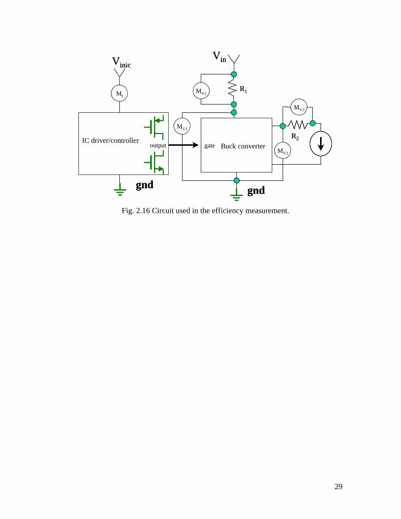
Fig. 2.16 shows the circuit used in the efficiency test of the buck converter. MBv1B, M Bv2 B,
M Bv3B and M Bv4 B are high-precision voltage meters. RB1 B and RB2 B are high-precision resistors.
The power consumed by the IC driver (usually, the driver and controller are monolithicly
integrated in one package) is given by
Minicic IVP ×= , (2.46)
where IBMB is the reading of the current meter MBIB. The average input current of the buck
converter is given by
1
1
RVIin = . (2.47)
Therefore, the input power from the voltage source VBinB is
1
21
RVVPin
×= . (2.48)

25
The output current is
2
3
RV
Iout = . (2.49)
Thus the output power is
2
43
RVV
Pout×
= . (2.50)
Then, the total power loss of the buck converter is
icoutinttloss PPPP +−= . (2.51)
Although the efficiency of the buck converter can be found by
icin
out
PPP+
=η (2.52)
or in
out
PP
=η , (2.53)
if we ignore the power loss of the driver, the components of the power loss are still not
known.
The major contributors of power loss in the buck converter are the inductor and
MOSFETs. The inductor loss includes the magnetic loss and resistive loss due to the
winding resistance. The MOSFETs’ loss includes the gate loss and the conduction and
switching losses. None of these loss components can be determined precisely by the
experiment. This is another reason why an accurate model of the buck converter is
needed.

26
Vsw Vin
0tSwitch
position: a b aDTs (1-D)Ts
Vsw Vin
0tSwitch
position: a b aDTs (1-D)Ts
Fig. 2.10 Waveform of the output voltage (Vsw).
Vin
gnd
Vout
High-side Driver High-side MOSFET
Low-sidediode
swL
CR
Vin
gnd
Vout
High-side Driver High-side MOSFET
Low-sidediode
swL
CR
Fig. 2.11 Equivalent circuit of the conventional buck converter.

27
Vin
gnd
Vout
High-side Driver
Low-side Driver
High-side MOSFET
Low-sideMOSFET
swL
CR
Vin
gnd
Vout
High-side Driver
Low-side Driver
High-side MOSFET
Low-sideMOSFET
swL
CR
Fig. 2.12 Equivalent circuit of the synchronous buck converter.
t0 t1 t2 t3 t4
Vgl
Vgh
Vdsl
Idl
Vdf
Vin
t
t
t
t
t0 t1 t2 t3 t4
Vgl
Vgh
Vdsl
Idl
Vdf
Vin
t
t
t
t
Fig. 2.13 Operating sequence of the synchronous buck converter (Part I).

28
t0 t1 t2 t3 t4
Vgl
Vgh
Vdsh
Idh
Vin
Vin+Vdf
Imax
t
t
t
t
t0 t1 t2 t3 t4
Vgl
Vgh
Vdsh
Idh
Vin
Vin+Vdf
Imax
t
t
t
t
Fig. 2.14 Operating sequence of the synchronous buck converter (Part II).
Vdsh
Pdsh
t
Vin
Idh
t
Iout
tτtn1 τtn2
t0 t1 t2 t3 t4 t5
τtn
τtf1 τtf2
τtf
Vdsh
Pdsh
t
Vin
Idh
t
Iout
tτtn1 τtn2
t0 t1 t2 t3 t4 t5
τtn
τtf1 τtf2
τtf Fig. 2.15 Simplified switching waveforms of the high-side MOSFET.
29
VinVinic
gnd gnd
R1
R2
MV1
MV3
Buck converterIC driver/controller
output gate
MV2
MV3
MI
VinVinic
gnd gnd
R1
R2
MV1
MV3
Buck converterIC driver/controller
output gate
MV2
MV3
MI
Fig. 2.16 Circuit used in the efficiency measurement.

30
Chapter 3 Analytical Modeling of the Buck Converter
Although the FEA-based mixed-mode simulation [B17] can provide more accurate results
than an analytical model [B11]-[B16], the latter is still indispensable, because the FEA model
looks like a black box, which contains many parameters. Without good understanding of the
effects of these parameters, the user may get lost in the simulation. In order to efficiently use
the FEA models, in this chapter, three analytical models related to the loss of the buck
converter are presented after the introduction of the basic model of the power MOSFET. The
first model links the switching loss of the high-side MOSFET to the design parameters of the
power MOSFET. The second is a novel circuit model used to calculate the turn-on and turn-
off loss of the high-side MOSFET of the buck converter with parasitic inductance. The last
models the dv/dt-induced spurious turn-on of the low-side MOSFET.
3.1 Modeling of the Power MOSFET in the Steady State
Modeling the power MOSFET [B1]-[B4] is not a trivial task. However, as a switch, the
power MOSFET has two states: off and on. When the gate-to-source voltage (VBgsB) is less than
the threshold voltage (VBth B), the current cannot flow from the drain to the source. However, the
current can travel from the source to the drain through the inherent body diode of the
MOSFET. Therefore, when the power MOSFET is off, it should be modeled as a diode. The
anode of the diode is the source of the MOSFET, and the cathode of the diode is the drain of
the MOSFET. There are two operation modes when the power MOSFET is on.
1) When VBgs B > VBt B and VBds B < VBgs B-VBt B, the MOSFET operates in the linear region. It can be
modeled as a voltage controlled resistor, the value of which is
pksubdft
thgsoxnchg
oxgds R
AR
AR
VVWTL
R +++−
=)(εµ
, (3.1)
where

31
• )( thgsoxnchg
oxg
VVWTL
−εµ is the channel resistance as expressed by Equation (2.5).
• RBdftB is due to the current spreading from the channel into the drift region as expressed
by the Equation (2.16).
• A is the device area.
• RBsub B is the contribution of the substrate.
• RBpk B is the package resistance, which is usually below 1 mΩ for the stat-of-the-art
package.
•
2) When VBgs B > VBt B and VBds B > VBgsB –VBt B, the MOSFET operates in the saturation region. It
behaves like a voltage-controlled current source, the value of which is
2)(21
thgsg
goxnchd VV
LW
CI −= µ . (3.2)
Due to the oxide gate and the depletion region of the silicon, the power MOSFET has
capacitances associated with the terminal. Usually, they are defined as follows.
• CBgs B is the capacitance between the gate and the source.
• CBgd B is the capacitance between the gate and the drain. CBgdB is also expressed as CBrss B.
• CBds B is the capacitance between the drain and the source.
• CBiss B = CBgs B + CBgd B is called input capacitance.
• CBoss B = CBds B + CBgd B is called output capacitance.
Fig. 3.1 shows the equivalent circuit of a power MOSFET, where the following definitions
apply,
• LBg B, LBd B and LBs B are the parasitic inductance associated with the package [C17]-[C21].
• RBg B includes the resistance of the gate bus inside the MOSFET and the package
resistance. The typical value of the gate bus is about 1 Ω, which is much larger than
the package resistance.
• RBd B is the sum of RBspd B, RBsubB and RBpk B.

3.2 Basic Switching Model of the High-side MOSFET in the Buck
Converter
The switching loss of the high-side MOSFET in the buck converter is a major part of the
total loss. In this section, the effect of the device characteristics on the switching performance
of the high-side MOSFET is addressed, based on the switching circuit with a clamped
inductive load.
3.2.1 Equivalent Circuit of the High-side MOSFET in the Buck Converter
The equivalent switching circuit of the high-side MOSFET in the buck converter is
basically a MOSFET with a clamped inductive load. However, this is not a straightforward
conclusion, and many people have requested further explanation of this point. Therefore, it is
worthwhile to dedicate several pages to explaining the derivation of the MOSFET with a
clamped inductive load from the buck converter.
The turn-on and turn-off of the high-side MOSFET occur when the low-side MOSFET is
off. Therefore, the low-side MOSFET can be simplified as a diode during the switching of the
high-side MOSFET. The driver of the high-side MOSFET is basically a CMOS buffer. If we
assume the following: that the NMOS and PMOS of the last stage of the buffer have the same
on resistance (Rdr); that the voltage source of the CMOS buffer is Vdr; and that the switching
time of the CMOS buffer is much shorter than that of the high-side MOSFET, then the driver
of the high-side MOSFET can be represented by resistor (Rdr) in series with a pulse voltage
source, the amplitude of which is Vdr. Therefore, the buck circuit shown in Fig. 2.12 can be
reduced to the circuit shown in Fig. 3.2, where the current ripple through the inductor L is
ignored, and the LCR network is simplified as a constant current source (Io). Since the
selection of the ground is arbitrary in the electrical circuit, we can define the switching node
(sw) as the ground as shown in Fig. 3.3. After swapping the positions of the input voltage
(Vin) and the parallels of the current source (Io) and diode, the switching circuit is rearranged
as shown in Fig. 3.4. If we use the power MOSFET model presented in section 3.1 to
32

substitute for the MOSFET symbol given in Fig. 3.4, we obtain a more complex circuit, as
shown in Fig. 3.5, where Rdrtt is the sum of Rdr and Rg, and Lg, Cds, Rd and Rs are ignored.
Therefore, the equivalent circuit of the high-side MOSFET is essentially a MOSFET with
a clamped inductive load, which is represented by a constant current, as shown in Fig. 3.5.
drain
source
gate
Rg Lg
Cgd
Cgs
Cds
Ld
Rd
Ls
Rs
drain
source
gate
Rg Lg
Cgd
Cgs
Cds
Ld
Rd
Ls
Rs
Fig. 3.1 The equivalent circuit of the power MOSFET.
33

34
gnd
High-side MOSFET
Body diode of thelow-side MOSFET (Dpbd)
sw
Io
Rdr
Vin
Vdr
gnd
High-side MOSFET
Body diode of thelow-side MOSFET (Dpbd)
sw
Io
Rdr
Vin
VdrVdr
(Low side MOSFET is simplified as a diode.)
Fig. 3.2 Equivalent circuit of the high-side MOSFET.
gnd
High-side MOSFETRdr
Vin
Body diode of the low-side MOSFET(Dpbd)
Io
Vdr
gnd
High-side MOSFETRdr
Vin
Body diode of the low-side MOSFET(Dpbd)
Io
VdrVdr
(The ground is moved from the anode of the diode to the cathode of the diode.)
Fig. 3.3 Equivalent circuit of the high-side MOSFET.

gnd
High-side MOSFET
Rdr
Vin
Io Dpbd
Vdr
gnd
High-side MOSFET
Rdr
Vin
Io Dpbd
Vdr
(The position of the input voltage Vin is swamped with the load Io.)
Fig. 3.4 Equivalent circuit of the high-side MOSFET.
gnd
High-side MOSFET
Rdrtt VinCgd
Cgs
Ld
Ls
Io
Dpbd
Vdr s
d
g
gnd
High-side MOSFET
Rdrtt VinCgd
Cgs
Ld
Ls
Io
Dpbd
Vdr s
d
g
(Major parasitic elements are included in the circuit.)
Fig. 3.5 Equivalent circuit of the high-side MOSFET.
35

36
gnd
High-side MOSFET
VinCgd
Cgs
Io
Dpbd
s
d
g
Ig
gnd
High-side MOSFET
VinCgd
Cgs
Io
Dpbd
s
d
g
Ig
Fig. 3.6 Equivalent circuit of the high-side MOSFET with constant current source as gate
driver.
3.2.2 Switching Process of MOSFET with Inductive Load
Although the equivalent circuit of the high-side MOSFET is much simpler to understand
than that of the original buck converter, it is still a high-order, nonlinear system. It is unlikely
that an analytical solution of the circuit illustrated in Fig. 3.5 can be found without any
assumptions or simplifications. In this section, the simplest analysis is presented in order to
achieve a basic concept of the switching process. More complex models are developed in
section 3.3 and section 3.4.
Fig. 3.6 ignores the parasitic inductance, and uses a current source as the gate driver to
further simplify the circuit. Three assumptions are made for the following discussion.
• The forward voltage drop of the freewheeling diode (DBpbdB) is zero
• CBgd B and CBgsB are constant
• The gate current (IBg B) is much smaller than the load current (IBo B)

37
3.2.2.1 Turn-on process
Fig. 3.7, Fig. 3.8 and Fig. 3.9 show the waveforms associated with the turn-on process.
1) Turn-on delay. From TB0 B to TB1 B, the MOSFET is off. Load current IBoB flows through the
diode (DBpbdB), and the drain voltage of the MOSFET equals the level of VBin B. Since a constant
current is applied on the gate, the gate-to-source voltage rises linearly as
tCI
Viss
ggs = . (3.3)
The total gate charge in this stage is
issthgs CVQ ×=1 . (3.4)
After VBgs B reaches the threshold voltage (VBthB), MOSFET starts to conduct, and the turn-on
process enters the second stage.
2) Current rising. In this period, the drain current starts to increase and finally reaches the
level of the total load current (IBoB). Since the free-wheeling diode (DBpbdB) is still on, the drain
voltage of the MOSFET is clamped at VBin B, and the MOSFET operates in the saturation state.
Referring to Equation (3.2), its drain current can be expressed as
22
2
21 t
CI
LW
CIiss
g
g
goxnchd µ= . (3.5)
This period comes to the end when IBd B is equal to load current (IBo B). The gate-to-source
voltage VBgs B is determined by
effthgson VVV += , (3.6)
where the effective gate voltage VBeffB is defined as
goxnch
goeff WC
LIV
µ2
= . (3.7)
The power loss on the MOSFET in this period is
g
gsoint
tisseff
goint
tdd I
QIVdtt
CVIIV
dtVIE 22
1
222
22
12 3
1∫∫ ==⋅= , (3.8)
where isseffgs CVQ =2 (3.9)

38
is the variation of the gate charge in this period.
After the MOSFET takes over all of the load current, the drain voltage starts to drop, and
the circuit enters the third stage.
3) Voltage falling. In this period, the drain current is equal to the load current (IBoB), and the
gate-to-source voltage remains at VBgsonB, as expressed in Equation (3.6), since the MOSFET
still operates in the saturation region. Because VBgs B is fixed at VBgsonB, the gate current only flows
through the gate-to-drain capacitance (CBgdB), and the voltage variation on C Bgd B is
tCI
Vgd
ggd =∆ . (3.10)
Therefore, the drain voltage is
tCI
VVVVgd
gingdind −=∆−= . (3.11)
Assuming that VBeffB is very small, the MOSFET remains in the saturation state until VBd B
reaches zero. Then, the duration of this period is
g
gd
IQ
ttt 02323 =−=∆ , (3.12)
where gdingd CVQ ×=0 (3.13)
is the variation of the gate charge in this stage. Therefore, the power loss in this period is
∫∫ =−==3
2
03
23 2
)(t
t g
gdino
gd
gino
t
tdd I
QVIdtt
CI
VIdtIVE . (3.14)
The MOSFET enters the linear region when VBds B is less than VBeffB and the MOSFET is in the on
state.
3.2.2.2 Turn-off process
The turn-off process starts when IBg B flows from the gate to the ground and the MOSFET
enters the saturation region. The turn-off process is basically the reverse order of the turn-on

39
process. Fig. 3.10, Fig. 3.11 and Fig. 3.12 show the waveforms associated with the turn-off
process.
(4) Voltage rising. This period is the reverse process of the third stage.
(5) Current dropping. This period is the reverse process of the second stage.
Two Equations, (3.8) and (3.14), describe the power loss in the switching process. EB2B
divided by EB3 B yields the ratio of the power loss in the second and the third stage, so
03
2
3
223
gd
eff
EEK == . (3.15)
Because usually QBeff B<< QBgd0B, we have EB2B << EB3B. Therefore, QBgd0B plays a very important role in
the total switching loss. In the next section, the origin of CBgdB and QBgd0B is related to the design
parameters of the UMOSFET.
Time
Vgs
Vth
Vgson=Vth+VeffVeff
Qgs1 Qgs2
Qgd0
Qsw
t1 t2 t3
∆t12 ∆t23
t0
∆t01
Time
Vgs
Vth
Vgson=Vth+VeffVeff
Qgs1 Qgs2
Qgd0
Qsw
t1 t2 t3
∆t12 ∆t23
t0
∆t01
Fig. 3.7 Waveform of VBgs B in the turn-on process of the MOSFET.

40
Vin
Id
Time
Vds
Io
t1 t2 t3t0
Vin
Id
Time
Vds
Io
t1 t2 t3t0 Fig. 3.8 Waveform of I Bd B and VBds B in the turn-on process of the MOSFET.
Pon=Vds×Id
∆t12 ∆t23
t0 t1 t2 t3
Time
Pon=Vds×Id
∆t12 ∆t23
t0 t1 t2 t3
Time
Fig. 3.9 Waveform of the power loss in the turn-on process of the MOSFET.

41
Vgs
Vth
Vgson=Vth+VeffVeff
Qgs1Qgs2
Qgd0
Qsw
t4 t5 t6
∆t45 ∆t56
t7
Time
Vgs
Vth
Vgson=Vth+VeffVeff
Qgs1Qgs2
Qgd0
Qsw
t4 t5 t6
∆t45 ∆t56
t7
Time
Fig. 3.10 Waveform of VBgs B in the turn-off process of the MOSFET
t4 t5 t6
∆t45 ∆t56
t7
Vin
Io
Time
Id
Vds
t4 t5 t6
∆t45 ∆t56
t7
Vin
Io
Time
Id
Vds
Fig. 3.11 Waveform of IBd B and VBdsB in the turn-off process of the MOSFET.

42
Poff=Vds×Id
Timet4 t5 t6
Poff=Vds×Id
Timet4 t5 t6 Fig. 3.12 Waveform of the power loss in the turn-off process of the MOSFET.
3.3 Modeling Gate-to-Drain Capacitance (C BgdB) and Charge (QBgdB)
As addressed in the preceding sections, for the high-side MOSFET, most of the switching
loss of the high-side MOSFET occurs during the charging and discharging of the gate-to-drain
capacitance CBgd B. Therefore, CBgd B plays an important role in the loss of the MOSFETs in the
buck converter, and it is important to understand the characteristics of CBgd B in the power
MOSFET.
The geometry of the gate to drain capacitance in the trench MOSFET is shown in Fig.
3.13, where CBgd B arises from the bottom of the trench and the part of the side wall of the trench,
that is not covered by the P-body area.
Because the minimum trench width WBch B is limited by silicon technology, WBch B is usually
much longer than Ovp, and the contribution of the side wall of the trench to the CBgd B is less
than that of the bottom of the trench. If we ignore Ovp and consider only the drain part
directly opposite to the bottom of the drain, CBgd B can be simplified as a one-dimensional
capacitor.

43
When the drain voltage is less than the gate voltage, VBdgB < 0, an accumulation layer is
formed under the oxide. Because the accumulation layer is very thin and highly conductive,
CBgd B equals to the oxide capacitance CBgdoxB, so
ox
oxgdoxgd T
CCε
== . (3.16)
In switching stage 3 and 4 as addressed in the preceding section, the gate voltage is VBgsonB;
when the drain voltage is less than VBgsonB, CBgd B can be treated as a constant value. However,
when the drain voltage is higher than the gate voltage, the depletion layer forms under the
gate oxide, which shares part of VBdgB. There are two cases for consideration.
• When the width of the depletion region is no more than the length of the drift region,
the electric field does not reach the highly doping substrate. It is called a non-punch-
through type of depletion.
• When the width of the depletion region is more than the length of the drift region, the
electric field reaches the highly doping substrate. It is called a punch-through type of
depletion.
Although, as demonstrated in the Appendix A, for both cases, the capacitance of the
depletion region is
dep
sidpl W
Cε
= , (3.17)
the expressions of WBdep B are different. Therefore, the derivations of CBgd B and QBgs B for non-punch-
through and punch-through types of depletion regions are discussed separately, as follows.
3.3.1 CBgdB and Q BgdB for the Non-Punch-Through Type of Depletion Region
The distributions of the electric field in the oxide and the non-punch-through type of
depletion region are shown in Fig. 3.14. The electric field in the oxide is a constant (EBoxB). So,
voltage on the gate oxide is
oxoxox TEV = . (3.18)
In the depletion region, the electric field drops linearly to zero, and its slope is

44
si
qNε
β = , (3.19)
where N is the doping concentration of the drift region. Then, the voltage on the depletion
region is
β2
2si
siE
V = . (3.20)
According to Gauss’s law, the ratio between the electric field on the oxide and the silicon
boundary is
ox
si
si
ox
EE
εε
α == . (3.21)
Therefore, the drain-to-gate voltage can be written as
β
α2
2si
oxsisioxdgE
TEVVV +=+= . (3.22)
The root of EBsi B in the above Equation is
oxdgoxsi TVTE αβββα −+= 2222 . (3.23)
Again, using Gauss’s law yields
)2( 2220 oxdgoxsisisigd TVTEQ αβββαεε −+== . (3.24)
Then, the width of the depletion region is
qN
TVT
qNQ
W oxdgoxsigddpl
)2( 222 αβββαε −+== . (3.25)
Finally, for the non-punch-through type depletion region, the gate to drain capacitance can be
expressed as
oxdpl
oxgd TW
Cα
αε+
= . (3.26)
3.3.2 CBgdB and Q BgdB for the Punch-Through Type of Depletion Region
The distribution of the electric field in the oxide and the non-punch-through type of
depletion region is shown in Fig. 3.15. The voltage on the gate oxide still can be expressed by
Equation (3.18). In the depletion region, the electric field still varies linearly, but it does not

45
drop to zero as is the case for the non-punch-through type. The voltage on the depletion
region is
2
2n
nsisiL
LEVβ
−= , (3.27)
where LBnB is the length of the depletion region. Then, the drain-to-gate voltage can be written
as
2
2n
nsioxsisioxdgL
LETEVVVβ
α −+=+= . (3.28)
The solution of EBsi B in the above Equation is
oxn
ndgsi TL
LVE
αβ
+
+=
25.0. (3.29)
Again, using Gauss’s law yields
oxn
ndgsisisigd TL
LVEQ
αβ
εε+
+==
2
0
5.0. (3.30)
As demonstrated in Appendix A, the capacitance of the punch-through type of depletion
region is constant. Therefore, the total gate-to-drain capacitance is
oxn
oxgd TL
Cα
αε+
= . (3.31)
Because when punch-through occurs, the width of the depletion region (WBdpl B) is equal to the
length of the drift region (LBn B), Equation (3.26) is a unified expression for both punch-through
and non-punch-through types of the depletion region.
An interesting result is that, although for the punch-through type of depletion region CBgd B is
constant,
gddggd CVQ ≠ . (3.32)
This is because the CBgd B is defined as
dg
gdgd dV
dQC = (3.33)
instead of

46
dg
gdgd V
QC = . (3.34)
If the CBgdB is defined by Equation (3.34), for the punch-through type of depletion region, CBgdB
depends on VBdg B. We can find the expression using Equation (3.30), such that
oxn
ndg
dg
si
dg
gdgd TL
LVVV
QC
αβε
+
+==
25.0. (3.35)
In this dissertation, the capacitance is always defined by (3.34).
The one-dimensional modeling and the two-dimensional simulation results of CBgd B are
compared in Fig. 3.16. When VBdg B is high, the simulation result is larger than that of the
calculation. This is due to the two-dimensional fringing effect. However, there is not much
overall difference between the calculation and simulation .
Fig. 3.17 shows the effects of the doping concentration (N) and the drift region length (LBn B)
on CBgd B. When LBn B is long, CBgd B is independent of LBn B, because, for the non-punch-through type of
depletion region, the depletion width is determined by voltage (VBdg B) and the doping
concentration of the depletion region. Since the width of the depletion region increases as the
doping concentration decreases (Equation 3.25), the lightly doped drift region has less CBgd B.
When LBn B is short, the width of the depletion region is L BnB. Therefore, shorter L BnB leads to more
CBgd B, and the doping concentration has no effect on CBgd B.
As shown in Fig. 3.18, LBn B and N have similar effects on QBgd0B. Two important conclusions
are that the punch-through type of the drift region is not good in terms of CBgd B and QBgd0B, and
the lightly doped drift region leads to less CBgd B and QBgd0B.

47
Wm/2 Wt/2
Ln
Pbd
N
Nsub
Tox
Ovp
Cox
Cdpl
Cgd
Wm/2 Wt/2
Ln
Pbd
N
Nsub
Tox
Ovp
Cox
Cdpl
Cgd
Fig. 3.13 One dimensional model of Cgd in the UMOSFET.
Tox
SiO2 Silicon
Eox
Esi
Wdpl
Slope = β
Tox
SiO2 Silicon
Eox
Esi
Wdpl
Slope = β
Fig. 3.14 Distribution of the electric field in the non-punch-through type of depletion
region.

48
Tox
SiO2 Silicon
Eox
Esi
Ln
Slope = β
Tox
SiO2 Silicon
Eox
Esi
Ln
Slope = β
Fig. 3.15 Distribution of the electric field in the punch-through type of depletion region.
0.0E+00
2.0E+04
4.0E+04
6.0E+04
8.0E+04
1.0E+05
1.2E+05
0 5 10 15 20Vdg (V)
Cgd
(pF/
cm2 )
Simulation results
Calculation results
Fig. 3.16 Comparison of calculated and simulated CBgd B.B

49
0.0E+00
5.0E+03
1.0E+04
1.5E+04
2.0E+04
2.5E+04
0 0.5 1 1.5 2 2.5Ln(um)
Cgd
(pF/
cm2 )
N=1e16N=2e16N=3e16
Vdg=17 V Tox=0.03um
Fig. 3.17 One-dimensional modeling of CBgd B.
150
200
250
300
350
400
450
500
0 0.5 1 1.5 2 2.5
Ln (um)
Qgd
0 (n
C/c
m2 )
N=1e16N=2e16N=3e16
Vdg=17 V Tox=0.03um
Fig. 3.18 One-dimensional modeling of QBgd0 B.

50
0
5
10
15
20
25
0 5 10 15time (ns)
Vds
(V) o
r Id (
A)
0
2
4
6
8
10
Vgs
(V)
VdsIdVgs
Fig. 3.19 Simulated turn-on waveforms.
3.3.3 Analysis of the Switching Process With Non-Constant C BgdB
The switching process of the MOSFET under the inductive load is described in section
3.2.2 with the assumption that the gate-to-drain capacitance (CBgdB) is constant. In this section,
the switching process is revised based on the CBgd B and QBgd B models developed in the preceding
section. Because the turn-off process is a reverse order of the turn-on process, only the turn-on
process is addressed in this section. The conclusions of the turn-on process are applicable for
the turn-off process.
Fig. 3.19 shows the general turn-on waveforms generated by Medici simulation. The main
difference between Fig. 3.19 and Fig. 3.8 is that in Fig. 3.8 the drain voltage drops linearly,
while in Fig. 3.19 the drain voltage drops quickly at the beginning, then has a slow linear
drop. This phenomenon is explained and described as follows.

51
1) Turn-on delay. From TB0 B to TB1 B, the MOSFET is off. Load current IBoB flows through the
diode (DBpbdB), and the drain voltage of the MOSFET equals the level of VBin B. When I BgB is applied
on the gate, the gate voltage will rise and the VBdg B will decrease. Fig. 3.16 shows that when VBdg B
is high, the variation of C Bgd B is not much. Therefore, the gate-to-source voltage rises linearly as
tCC
It
CI
Vgdgs
g
iss
ggs +
≈= , (3.36)
where CBgdB is expressed by Equation (3.26). The total gate charge in this stage is
)(1 gdgsthgs CCVQ +×= . (3.37)
It takes
g
gs
IQ
t 101 = (3.38)
for VBgs B to reach the threshold voltage (VBth B). Then, the MOSFET starts to conduct, and the
turn-on process enters the second stage.
2) Current rising. In this period, since the drain voltage of the MOSFET is clamped at VBin B,
CBgd Bcan still be approximated by Equation (3.26). For the non-punch-through type of depletion
region, we can use V BdgB = VBin B-VBthB to find the depletion width (WBdpl B); for the punch-through
type of depletion region, the depletion width equals the length of the drift region (LBnB).
Since CBgdB is assumed to be constant, the derivation in the section (3.2.2) is still valid. The
power loss on the MOSFET in this period is
g
isseffoings I
CVIVE
31
2 = . (3.39)
It takes
g
gseffgs I
CVt =2 (3.40)
for VBgs B to reach
effthgson VVV += . (3.41)
Then, the drain voltage starts to drop and the circuit enters the third stage.
3) Voltage falling. At the beginning of this period, the drain-to-gate voltage is

52
gsonindg VVV −=0 . (3.42)
The expression of the initial gate-to-drain charge QBgd0B depends on whether the depletion
region is the punch-through type. If the depletion region is punched through, Equation (3.30)
should be used to determine QBgd0B; otherwise Equation (3.24) should be used. Since a constant
current is applied on the gate, the variation of the gate-to-drain charge QBgd Bis
tIQQ ggdgd −= 0 . (3.43)
For the punch-through type of depletion region, the drain voltage can be derived using
Equation (3.30), such that
)(2
)(2
0effth
noxn
si
ggdd VVLTL
tIQV ++−+
−=
βαε
. (3.44)
As QBgd B continues to decrease, the depletion region will change into the non-punch-through
type, so
2
singd
LQ
εβ= . (3.45)
Canceling QBgdB from Equation (3.43) and (3.45) yields
g
singdpt I
LQt
εβ5.00 −= . (3.46)
This is the time period needed for the punch-through type of depletion region to change into
the non-punch-through type. In Equation (3.46), 0)5.0( 0 <− singd LQ εβ (or 0<ptt ) means the
initial depletion region is the non-punch-through type. Then, tBpt B should be zero instead of
negative, so the following Equation expresses tBpt B correctly
g
singdsingdpt I
LQLQt
2
5.0)5.0( 00 εβεβ −+−= . (3.47)
Therefore, the power loss in this stage is
pteffthnsi
oxnptgptgd
t
dopt tVVLTLtItQdtVIEpt
)5.0()5.0( 220
0
−−−+
−== ∫ βε
α . (3.48)
After the punch-through type of depletion region changes into the non-punch-through type,
Equation (3.24) can be used to find that the drain voltage varies as
)()(
2)( 0
2
20
effthox
oxggd
si
ggdd VV
TtIQtIQV ++
−+
−=
εβε (3.49)

53
It takes
ptg
gdnpt t
IQ
t −= 0 (3.50)
for the drain voltage to drop to the level of the gate voltage ( effth VV + ). The power loss in this
period is
),)(()](5.0)([
2
)()()(3
220
2
20
220
332
pddpleffthpddplgpddplgdOX
ox
si
pddplgdpddplgdgpddplg
tt
tdonpt
ttVVttIttQT
ttQttQIttI
dtVIEnptpt
pt
−++−−−+
−+−−−== ∫
+
ε
βε (3.51)
where nptptdpl ttt += (3.52)
is the total time needed to extract the charge of the drift region. Therefore, the total loss
during the depletion region discharge is
nptptdpl EEE += (3.53)
After t BdplB, the depletion region disappears, and the drain voltage continues dropping, as
gdox
geffthd C
tIVVV −+= )( , (3.54)
where CBgdoxB is defined in Equation (3.16). Therefore, it takes
g
gdoxthox I
CVt = (3.55)
before the MOSFET enters the linear region. The power loss during tBox B is
g
gdoxtheffthot
doox ICVVVI
dtVIEox
2)2(
0
+== ∫ , (3.56)
and the total power loss in this stage is
oxdplqgd EEE += . (3.57)
4) After the third stage, the MOSFET is on, and the gate voltage continue to rise as
tCC
IVVV
gdoxgs
geffthgs +
++= . (3.58)
Since the MOSFET operates in the linear region, the drain voltage is

54
thgs
effd VV
VV
−=
2
. (3.59)
In the four stages of the turn-on process, the power loss occurs only during the second and
third stages. Therefore, the total turn-on time is
oxdplgstn tttt ++= 2 , (3.60)
and the total turn-on loss is
oxdplgstn EEEE ++= 2 . (3.61)
3.3.4 Worked Examples of the Switching Process with Non-Constant CBgd
Band QBgdB
In order to illustrate the different waveforms expressed by the analytical expressions that
have been derived, it is worthwhile to work through some numerical examples. Initially, a set
of typical MOSFET and application parameters are used. Then, the effects of the doping
condition and gate oxide on the power loss are examined. The chosen parameters are based on
the mainstream commercial high-side MOSFET, as follows.
• Input voltage VBin B = 20 V
• Output current IBo B = 10 A
• Current of the gate driver IBg B = 1 A
• Total area of the gate to drain capacitance AA = 1.04 mmP
2P
• Threshold voltage of the MOSFET V Bth B = 1.58 V
• The effective gate voltage VBeffB = 0.46 V
• Gate to source capacitance CBgsB = 1280 pF
• Thickness the gate oxide TBoxB = 300 Å
• Doping concentration of the drift layer N = 2×10P
16P cmP
-3P
• Width of the drift region LBn B = 0.8 µm
In order to show the accuracy of the analytical modeling, both the calculation and
simulation results are listed in table (3.1).

Table 3.1 Calculation and simulation results of the example.
Variable name Simulation
results
Calculation
result
Related
Equation
Delay time: t01 2.23 ns 2.22 ns (3.39)
Current rising time: tgs2 0.65 ns 0.65 ns (3.41)
Power loss during current rise: Egs2 46.5 nJ 43.2 Nj (3.40)
Depletion time: tdpl 4.13 ns 3.56 ns (3.53)
Depletion loss: Edpl 361 nJ 309 nJ (3.54)
Discharging time of Cox: tox 2.17 ns 2.00 ns (3.56)
Discharging loss of Cox: Eox 21.8 nJ 24.8 nJ (3.57)
Total turn-on time: ttn 6.95 ns 6.51 ns (3.61)
Total turn-on loss: Etn 430 nJ 378 nJ (3.62)
The calculated waveform of power loss is compared with the simulation result in Fig. 3.20.
Due to the fringing effect of Cgd, the simulated loss is more than that of the calculation.
However, the analytical model properly describes the key steps of the turn-on process. Based
on the analytical model, some design issues of the MOSFET are discussed as follows.
(1) Punch-through design or non-punch-through design of the drift region
At the end of section 3.3.2, we conclude that the punch-through type of drift region has
more Qgd0 than that of the non-punch-through type of design. Since Qgd0 plays a very
important role in the turn-on loss, the effect of the punch-through on the turn-on loss should
be addressed. Fig. 3.21 shows that the punch-through results in more turn-on loss; Fig. 3.22
illustrates the waveforms of power loss for three different designs. From the calculation, we
can conclude that the punch-through results in more turn-on loss than the non-punch-through
design.
(2) Effect of the doping concentration of the drift region.
For the non-punch-through design, Fig. 3.18 shows that the lightly doped drift region has
less charge. Therefore, we can expect the turn-on power loss to decrease as the doping
concentration of the drift region decreases, as shown in Fig. 3.23 and Fig. 3.24.
55

(3) Effect of the thickness of the gate oxide.
Although thicker gate oxide leads to less Qgd0, its effect on the turn-on loss is not as great
as the doping concentration of the drift region. As shown in Fig. 3.25 and Fig. 3.26, the turn-
on loss only drops significantly at the end of the turn-on process. This is because at the
beginning of the turn-on process, the width of the depletion region is longer than Tox, and Tox
does not have much effect on Cgd or the power loss.
From the switching loss standpoint, it is better to use the non-punch-through design, a
lightly doped drift region and thicker gate oxide. However, the latter two design trends
negatively impact the conduction loss of the MOSFET. The discussion of the design
optimization will be presented in Chapter 4, in which the FEA model is employed to more
accurately calculate the power loss.
0
50
100
150
200
250
0 2 4 6 8 10time (ns)
Pow
er L
oss
(W)
12
Calculation results
Simulation results
Fig. 3.20 Comparison of the simulation and calculation results.
56

57
200
300
400
500
600
700
800
900
0 0.2 0.4 0.6 0.8 1 1.2Length of the drift region (Ln)
Turn
-on
loss
(nJ)
Example of Table 3.1
Punch-through
Non-punch-through200
300
400
500
600
700
800
900
0 0.2 0.4 0.6 0.8 1 1.2Length of the drift region (Ln)
Turn
-on
loss
(nJ)
Example of Table 3.1
Punch-through
Non-punch-through
Fig. 3.21 Effect of the punch-through on the turn-on loss.
0
50
100
150
200
250
0 2 4 6 8 10
time (ns)
Pow
er lo
ss (W
) Ln=0.4Ln=0.6Ln=1.0
Non-Punch-through
punch-through
0
50
100
150
200
250
0 2 4 6 8 10
time (ns)
Pow
er lo
ss (W
) Ln=0.4Ln=0.6Ln=1.0
Non-Punch-through
punch-through
Fig. 3.22 Effect of the punch-through on the turn-on loss.

200
250
300
350
400
450
0.E+00 1.E+16 2.E+16 3.E+16
Doping concentration of the drift region (cm-3)
Pow
er lo
ss (n
J)
Fig. 3.23 Effect of the doping concentration on the turn-on loss.
0
50
100
150
200
250
0 2 4 6 8
time (ns)
Pow
er lo
ss (W
)
10
N=1e16N=2e16N=3e16
Fig. 3.24 Effect of the Doping concentration on the turn-on loss.
58

59
320
340
360
380
400
0 20 40 60 80
Thickness of the gate oxide (nm)
Pow
er lo
ss (n
J)
Fig. 3.25 Effect of the thickness of the gate oxide on the turn-on loss.
0
50
100
150
200
250
0 2 4 6 8 10time (ns)
Pow
er lo
ss (W
) Tox=30nTox=50nTox=70n
Fig. 3.26 Effect of the thickness of the gate oxide on the turn-on loss.

60
3.4 A Novel Model for MOSFET Switching Loss Calculation
In this section, a novel model for MOSFET switching loss calculation is presented, which
takes into account the major parasitic elements ignored in Equations (3.2) and (3.3), providing
more insight into the MOSFET switching process.
There are several papers dealing with the switching process of the MOSFET [B16], [B18]-
[20]. However, no paper calculates the effect of LBs B directly. The conclusion of the influence of
LBs B is that the LBs B introduces an additional resistance into the gate circuit. Fig. 3.27 shows the
general turn-on waveforms of IBd B, VBds B and VBgs B. As described before, the shape of VBds B is far from
a straight line. The platform of VBds B leads to more power loss. In this section, a new method is
provided to calculate the switching loss. Two assumptions are made in the following analysis:
the capacitance value of CBgd B and CBgs B have fixed values; and The forward voltage drop of diode
DBpbdB is VBfdB.
3.4.1 Analysis of the Turn-on Process
Based on the waveforms shown in Fig. 3.27, the turn-on process can be divided into the
following four stages.
(1) Turn-on delay. In this period, the MOSFET is off. The current flows through the diode
(DBpbdB), the voltage drop on the inductor LBd B is zero, and the voltage on the MOSFET drain is
fdind VVV +=1 . (3.62)
Ignoring the small gate current through the inductor LBs B, the circuit can be reduced to the one
shown in Fig. 3.28. Because when VBds B is high, CBgs B>>CBgdB, CBgdB can be ignored. It takes time T Bd B
for the gate voltage VBgs B to ramp up to the level of VBt B, such that
)ln(tdr
drgd VV
VT
−= τ , (3.63)
where
gsdrttg CR=τ . (3.64)

61
Since there is no current through the MOSFET, the loss is zero in this period.
(2) IBdB rises from 0 to I Bo B. At the beginning of this period, VBds B drops sharply and then stays at
a rather constant value (VBds0B). In order to find out the value of VBds0B, the equivalent circuit
depicted in Fig. 3.29 is employed, where CBgd B is removed because CBgdB<< CBgs B, and the Miller
effect is insignificant when VBdsB does not change much. In addition, the MOSFET is replaced
with a voltage-controlled current source. Since the MOSFET works in the saturation region,
the drain current can be expressed as
2)( tgsd VVKI −= . (3.65)
Because the current still goes through diode DBpbdB, the voltage on the node d′ is clamped to
fdinclp VVV += . (3.66)
Therefore, a voltage source VBclpB is connected to the node d’ directly, and both the current
source Io and the diode D BpbdB are removed from the equivalent circuit.
On the other hand, when the MOSFET operates in the saturation region, the small-signal
model of the MOSFET is
effmds VgI = , (3.67)
where the transconductance gBmB is
effm KVg 2= . (3.68)
In this case, it is easy to show that the input impedance has the following form in the S
domain [E8]:
gs
sgs
smdrttin sC
sLCL
gRZ 1+++= . (3.69)
At time zero, assume that a step change (VBdrB) occurs at the gate supply voltage. Since gBmB is
very small when VBgs B is small, at the beginning the term gBmBLBs B/CBgsB can be ignored. For the state-
of-the-art 30V MOSFET, the typical value of RBdrttB is from 2 to 4 Ω; Ls is from 1 to 2 nH; CBgs B
is from 1n to 4nF. For simplicity, we ignore the effect of LBs B on ZBin B, so the effective gate
voltage (V BeffB = VBgs B – VBt B) and the voltage on RBdrttB take the form
)1( / gtdreff eVV τ−−= , (3.70)

62
and tgt
drdrtt VeVV −= − τ/ , (3.71)
respectively, where the time constant τ BgB is defined in Equation (3.64).
In order to determine the voltage VBds0 B, we need to know when VBds B comes to a relatively
stable value. Fortunately, the accuracy of the time (TB0 B) is not critical, because VBdsB does not
vary much in the vicinity of T B0B. Assuming VBds B becomes stable when VBeff B= VBrg B, substituting
(3.72) into (3.71) yields
)2
ln(0tdr
drgsdrtt VV
VCRT
+≈ . (3.72)
However, from time 0 to time TB0 B, gBmB rises rapidly. Since the time constant τBg B is not actually a
constant, referring to Equation (3.69), a more precise expression for the time constant can be
written as
gsgs
smg C
CL
gR )( +=τ . (3.73)
Ignoring RBg B and substituting Equation (3.68) into (3.73) yields
seff LKV2=τ . (3.74)
A much more important approximation can be made, by reducing Equation (3.70) to the first
order and then using Equation (3.74) to replace τ BgB. This leads to
ts
drgs V
KLtV
V +=2
. (3.75)
Then, at time TB0 B, VBgs B is
ts
drgs V
KLTV
V +=2
00 . (3.76)
Because VBeff B= VBrg B is assumed, at time T B0 B, the voltage drop on RBg B is
s
drdrtt KL
TVV
20
0 = , (3.77)
and the voltage on the source inductance LBs B is
ts
drdrdrttgsdrls V
KLTV
VVVVV −−=−−=2
2 00000 . (3.78)
Next, we know that the di/dt of LBs B is

63
s
lso
LV
=α . (3.79)
Ignoring the gate current, LBd B has the same di/dt as LBs B, and the voltage on L Bd B is
s
dlsld L
LVV 00 = . (3.80)
Finally, we find the voltage VBds0B,
)1(00s
dlsclpds L
LVVV +−= . (3.81)
Equation (3.81) is valid when VBds0 B> VBeffB. Because the maximum value of VBls0 B is VBdrB, and LBd B <
LBs B, VBds0 B> VBeffB means that VBinB>2VBdrB, which is true for the high-step-down DC-DC buck
converter. The time needed for the current rising to I BoB is
0
2ls
soo
VLII
T ==α
. (3.82)
Then, the power loss in the second stage is
0
02
022 5.05.0ls
dssodso V
VLIVITE == . (3.83)
(3) After IBdB reaches IBo B, the turn-on process enters into the third stage. The MOSFET is still
in the saturation state. if we ignore the gate current, its drain current is equal to the level of IBo B.
Because IBdB is rather stable in this period, LBs B and LBdB can be removed. The CBgs B also can be
ignored because voltage VBgs B is almost unchanged, and is determined by
to
gs VKI
V +=3 . (3.84)
The equivalent circuit for this period is shown in Fig. 3.30. The current through CBgd B is equal to
the current through RBdrttB, so
drtt
gsdrdrttcgd R
VVII 3−
== . (3.85)
The voltage on the drain of the MOSFET is
tCI
VVVVgd
cgddscgddsd −=−= 003 . (3.86)

64
where VBds0B is the initial voltage expressed by Equation (3.82). The time interval (TB3 B) for the
drain voltage to drop from VBds0 B to 0 V is
gdgsdr
ds
cgd
gdds
VVV
ICV
T τ3
003 −
== , (3.87)
where
gdggd CR=τ . (3.88)
The power loss for this period is
033 5.0 dsoVITE = . (3.89)
(4) After VBds B drops below VBeff B, the MOSFET enters the linear region. VBgs B continues rising
to the level of VBdrB, soB
iss
gsdrgsisst
gsdrgsgstVVVeVVVV
ττ )()1)(( 33
/31 −+≈−−+= − , (3.90)
where the time constant τ Biss B is
issgiss CR=τ . (3.91)
Based on the first-order approximation made in Equation (3.90), it takes time interval TB4 B = τ Biss B
to finish the fourth stage. Because the MOSFET works in the linear region, it can be modeled
as a voltage-controlled resistor, as shown in Fig. 3.31:
)(2
1
tgsds VVK
R−
= . (3.92)
Because the current through the MOSFET is IBoB, VBds B is given by
)(2 tgs
ods VVK
IV
−= . (3.93)
Then, the power loss in this phase is
tgs
tdriss
gsdr
oissdso VV
VVVVK
IdtVIE
−−
−== ∫
30 3
2
4 ln)(2
τ τ. (3.94)

65
Fig. 3.27 General switching waveforms.
gnd
RdrttVin+VfdCgd
CgsVdr
s
d
g
Cgs>>Cgd
gnd
Rdrtt Cgs
Vdrs
g
gnd
RdrttVin+VfdCgd
CgsVdr
s
d
g
Cgs>>Cgd
gnd
Rdrtt Cgs
Vdrs
g
Fig. 3.28 Equivalent circuit of turn-on process.

66
gnd
Rdrtt
Cgs
Ls
Vdrs
d
g
Vin+Vfd
Ld
d`
2)( tgsds VVKI −=
gnd
Rdrtt
Cgs
Ls
Vdrs
d
g
Vin+Vfd
Ld
d`
2)( tgsds VVKI −=
Fig. 3.29 Equivalent circuit of turn-on process.
gnd
Rdrtt Cgd
Ls
Io
Vdrs
d
g
gnd
Rdrtt Cgd
Ls
Io
Vdrs
d
g
Fig. 3.30 Equivalent circuit of turn-on process.

67
gnd
Rdrtt
Ciss
Io
Vdr s
d
g)(2
1
tgsds VVK
R−
=
gnd
Rdrtt
Ciss
Io
Vdr s
d
g)(2
1
tgsds VVK
R−
=
Fig. 3.31 Equivalent circuit of turn-on process.
3.4.2 Analysis of the Turn-off Process
Although the turn-off process is a reverse order of the turn-on process, its gate driving
condition is not the same as that of the turn-on process. In the turn-on process, the gate current
is driven by the voltage of VBdrB, while in the turn-off process, the gate is shorted to the ground.
(5) At the beginning of the turn-off process, as shown in Fig. 3.32, IBdB remains at IBo B, and
there is little variation in the level of VBds B is not much. The VBgs B drops exponentially, as
isstdrgs eVV τ/−= . (3.95)
Since the MOSFET is in the linear region, VBdsB is determined by Equation (3.93). As a first-
order approximation, we can use Equation (3.95) to determine the time needed for the
MOSFET to leave the linear region, so
issdr
gs
VV
T τ)1( 35 −= . (3.96)
Then, the power loss in this period is

68
tgs
tdr
dr
issoT
dso VVVV
KVI
dtVIE−−
== ∫3
25
05 ln
2τ
. (3.97)
(6) When the MOSFET enters the saturation region, the equivalent circuit depicted in Fig.
3.33 applies. It is rather like the second stage of the turn-on process. The difference is that the
current through RBdrttB (or the current through CBgdB) is
drtt
gsdrttcgd R
VII 3== . (3.98)
The voltage on the drain of the MOSFET can be expressed as
)1(3gdg
gsds CRtVV += . (3.99)
This stage comes to an end when VBds B reaches VBin B+VBfdB; therefore the time interval for this
phase is
gdgs
gsfbin
VVVV
T τ3
36
−+= . (3.100)
Then, the power loss in this period is
636 )(5.0 TIVVVE ofbings ++= . (3.101)
(7) After VBds B reaches VBin B + VBfd B, the current starts to drop. Because in this phase the VBds B is
rather stable, the effect of CBgd B can be ignored, and the equivalent circuit shown in Fig. 3.34
applies. After ignoring the inductive part sLBs B, VBgs B takes the following form:
τt
gsgs eVV−
= 3 , (3.102)
where the time constant τ is
sgsgsgsmgsg LKVCRLgCR 2+=+=τ . (3.103)
Actually, τ is not a constant, and the minimum value of τ is
gsgg CR=τ . (3.104)
If we expand Equation (3.102) to the first order and use τBg B to replace the variable τ, we obtain
)1(3g
gsgstVV
τ−= . (3.105)

69
Since the MOSFET is in the saturation region, the current through the MOSFET can be
expressed as
2
2
3 )1()1( tIVtVKI otg
gsd ⋅−=⎥⎥⎦
⎤
⎢⎢⎣
⎡−−= β
τ, (3.106)
where gtgs
gs
VVV
τβ
)( 3
3
−= . (3.107)
Respectively, the voltages on LBs B and LBd B are
⎥⎥⎦
⎤
⎢⎢⎣
⎡−−== t
VVV
VKLdt
dILVg
gstgs
g
gssdsls ττ
33
3 )(2
, (3.108)
and ⎥⎥⎦
⎤
⎢⎢⎣
⎡−−== t
VVV
VKLdt
dILVg
gstgs
g
gsdddld ττ
33
3 )(2
. (3.109)
Then, we can find the expression of VBds B, such that
tVVVVVV ldlsfdinds ⋅−=+++= γmax , (3.110)
where )()(2
33
max tgsg
gsdsfdin VV
VLLKVVV −
+++=
τ, (3.111)
and 2
23)(2
g
gsds VLLKτ
γ+
= . (3.112)
This period comes to the end when VBgs B drops to VBtB. Therefore, we can find the duration from
Equation (3.105), as follows
ggs
t
VVT τ)1(
37 −= . (3.113)
The power loss in this period is
⎥⎦
⎤⎢⎣
⎡+
+−
++
⋅−== ∫ 7max
27max
37
2max
47
2
07 2
)2(3
)2(4
7
TVTVTVTIdtIVE o
T
ddsβγββγγβ . (3.114)
(8) When VBgs B drops below VBtB, the MOSFET turns off. Since VBdsB is high, CBds B can be
ignored, and the input capacitor CBgs B continues to discharge through the resistor RBdrttB (Fig. 3.35)
until VBgs B reaches zero. Because
gttgs eVV τ/−= , (3.115)
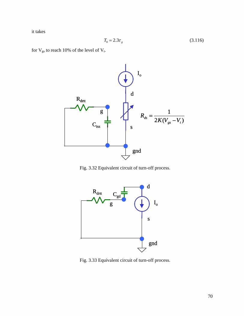
70
it takes
gT τ3.28 = (3.116)
for VBgs B to reach 10% of the level of VBtB.
gnd
Rdrtt
Ciss
Io
s
d
g)(2
1
tgsds VVK
R−
=
gnd
Rdrtt
Ciss
Io
s
d
g)(2
1
tgsds VVK
R−
=
Fig. 3.32 Equivalent circuit of turn-off process.
gnd
Rdrtt Cgd
Io
s
d
g
gnd
Rdrtt Cgd
Io
s
d
g
Fig. 3.33 Equivalent circuit of turn-off process.

71
gnd
Rdrtt
Cgs
Ls
s
d
g
Vin+Vfd
Ld
d`
2)( tgsds VVKI −=
gnd
Rdrtt
Cgs
Ls
s
d
g
Vin+Vfd
Ld
d`
2)( tgsds VVKI −=
Fig. 3.34 Equivalent circuit of turn-off process.
gnd
Rdrtt
Cgs
s
g
gnd
Rdrtt
Cgs
s
g
Fig. 3.35 Equivalent circuit of turn-off process.
3.4.3 Worked Example of the Switching Process
In this section, the effects of the parasitic inductance on the switching loss are examined.
The chosen parameters are as follows.
• Input voltage VBin B = 20 V
• Clamping voltage VBclp B = 2.2 V

72
• Output current IBo B = 10 A
• Gate drive current IBg B = 1 A
• Gate drive voltage VBdrB = 5 V
• Threshold voltage VBtB = 1.73 V
• Gate-to-source capacitance CBgsB = 0.72 nF
• Gate-to-drain capacitance CBgdB = 28.6 pF
• K = 3.3 A/VP
2P
The effects of LBs B and LBd B on the switching loss are shown in Fig. 3.36 and Fig. 3.37,
respectively. Larger LBs B results in more turn-on and turn-off losses, but the switching loss is
not sensitive to LBd B. However, LBdB leads to more voltage stress in the turn-on process, as
expressed in Equation (3.111). Therefore, both LBs B and LBdB should be minimized in the package
and circuit design.
0.3
0.4
0.5
0.6
0.7
0.7 0.9 1.1 1.3 1.5Source inductance (nH)
Loss
(uJ)
Turn-on lossTurn-off loss
Fig. 3.36 Effect of LBs B on the switching loss (LBd B = 0.8 nH).

73
0.200
0.300
0.400
0.500
0.600
0.50 0.70 0.90 1.10 1.30Drain inductance (nH)
Loss
(nJ)
Turn-on lossTurn-off loss
Fig. 3.37 Effect of LBd B on the switching loss (LBs B = 1.2 nH).
3.5 Analysis of dv/dt-Induced Spurious Turn-on of the MOSFET
In the preceding sections, the switching loss of the high-side MOSFET is analyzed. It
seems that the loss of the high-side MOSFET is more difficult to model than that of the low-
side MOSFET, since the dominant loss of the low-side MOSFET is the conduction loss.
However, the low-side MOSFET suffers another dv/dt-induced loss [B21]-[B23], which is
even more complex than the switching process of the high-side MOSFET.
When the high-side MOSFET is turning on, the drain voltage of the low-side MOSFET
rises rapidly. This means the drain of the low-side MOSFET has a high-dv/dt condition,
which will lead to an increase in the voltage of the gate of the low-side MOSFET. If the dv/dt
is large enough, the low-side MOSFET will be turned on again even though its gate is tied to
the ground by the driver. Because this is a high-order nonlinear problem, it is very difficult to
determine the loss related to this type of dv/dt-induced turn-on. In this section, an analytical
model is presented to calculate the spurious turn-on voltage. The analysis of the spurious turn-
on loss is performed in Chapter 4 by FEA.

74
The equivalent circuit of the MOSFET in this case is shown in Fig. 3.38, where RBgs B
includes both the gate resistance of the power MOSFET and the pull-down resistance of the
driver. Since the MOSFET is off before the spurious turn-on occurs, the MOSFET can be
removed from the circuit (Fig. 3.39). Because the general solution of the problem leads to
fourth order differential Equations, we have to simplify the problem by ignoring the less
important parasitic components and consider their effects later. The estimation of parasitic
components is based on the 20V to 30V state-of-the-art MOSFET, for which LBgB >> LBs B and LBd B,
and CBgs B>>CBgd B and CBds B. Because the impedance from node G to the ground is much larger than
that from node S to the ground and CBgs B>>CBgd B, Fig. 3.39 can be reduced to the circuit
illustrated in Fig. 3.40 and Fig. 3.41. In Fig. 3.41, the total impedance from node D to the
ground is
sCCLsZ ds
D12 +
= , (3.117)
where ossdsgddsgdgs
gdgs CCCCCCCC
C =+≈++
⋅= , (3.118)
and sdds LLL += . (3.119)
Assuming a linearly rising voltage is applied to the drain, such that
KtVin = , (3.120)
then the total current in the s domain can be expressed as
⎟⎟⎠
⎞⎜⎜⎝
⎛+
−=+
== 20
221
1 ωss
sKC
CLsC
sK
ZVI oss
ossds
oss
D
int , (3.121)
where
ossdsCL
10 =ω . (3.122)
Next, the current through the capacitor CBgdB can be found by:
)1( 20
2 ω+−==
ss
sKC
CCI
I gdoss
gdtgd , (3.123)

75
and the voltage on node S is
12 +
==ossds
ossssts CLs
CKLsLIV . (3.124)
Both current IBgd B and voltage Vs contribute to the gate-to-source voltage VBgs B. We first
calculate the VBgs B generated by the current IBgdB based on the circuit depicted in Fig. 3.42, where
the node S is connected directly to the ground. The influence of voltage VBs B on voltage VBgs B will
be taken into account later. In order to simplify the calculation, the current IBgdB is split into two
parts, as follows
cgdaccgddcgd III += , (3.125)
where IBgddcB represents the constant DC current
s
KCI gdgddc1
= , (3.126)
and IBgdacB represents the AC current
20
2 ω+−=
ssKCI gdgdac . (3.127)
The impedance from G to the ground is
12 ++
+=
gsgsgsg
ggsg CsRCLs
sLRZ . (3.128)
Therefore, VBgs B, excited by the DC component of I BgdB, is
)1( 2 ++
+=⋅=
gsgsgsg
ggsgdgcgddcgsdc CsRCLss
sLRKCZIV . (3.129)
The VBgsdcB in the time domain is
⎥⎥⎦
⎤
⎢⎢⎣
⎡ −+−⋅= −− te
CLCRL
teRCKV t
gsg
gsgsgtgsgdgsdc ω
ωω ττ sin
22
)cos1( /2
/ , (3.130)
where gs
g
RL2
=τ , (3.131)
and 2
2
41
g
gs
gsg LR
CL−=ω . (3.132)

76
The VBgs B, excited by the AC component of I BgdB, is
122
02 ++
+⋅
+⋅⋅−=⋅=
gsgsgsg
ggsgdgcgdacgsac CsRCLs
sLRs
sCKZIVω
. (3.133)
In order to simplify the solution, we assume that gsgsg CRL 2>> , so the expression of VBgsacB in
the time domain is
⎥⎦
⎤⎢⎣
⎡+−−= tLtt
RKCV gg
gsggdgsac 00
00
2
sin)cos(cos ωωωωω
ω, (3.134)
where gsg
g CL1
=ω . (3.135)
Since Rgs/ω0<<Lg, Vgsac can be reduced to
tCKL
V ggdggsac 0
0
2
sin ωω
ω−= . (3.136)
The sinusoidal voltage at node S, expressed by Equation (3.124), also gives rise to the
voltage VBgsB. From nodes S to G, CBgs B provides a path with the least impedance. Therefore, we
can use the simplified circuit (Fig. 3.43) to find the voltage VBgs B generated by VBs B, which in the
s domain is given by
111
220
220 +++
−=gsgsgsg
osssgss CsRCLssCLKV
ωω . (3.137)
With the assumption that gsgsg CRL 2>> , the solution of VBgss B in the time domain can be
approximated as
⎥⎥⎦
⎤
⎢⎢⎣
⎡−−=
−
tetCLCKL
Vt
gggsg
osssgss 0
0
/
sinsin1 ωω
ωω
τ
. (3.138)
The total VBgs B is the sum of VBgsdcB, VBgsacB and VBgss B, so
gssgsacgsdcgs VVVV ++= . (3.139)
The typical waveform of VBgs B and its three components are shown in Fig. 3.44. The peak value
of Vgs can be approximated as
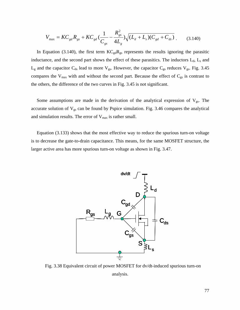
77
))(()4
1(2
max dsgdsdg
gs
gsgdgsgd CCLL
LR
CKCRKCV ++−+= . (3.140)
In Equation (3.140), the first term KC Bgd BRBgs B represents the results ignoring the parasitic
inductance, and the second part shows the effect of these parasitics. The inductors LBd B, LBs B and
LBg B and the capacitor CBds B lead to more VBgs B. However, the capacitor CBgsB reduces VBgsB. Fig. 3.45
compares the VBmax B with and without the second part. Because the effect of CBgs B is contrast to
the others, the difference of the two curves in Fig. 3.45 is not significant.
Some assumptions are made in the derivation of the analytical expression of VBgsB. The
accurate solution of VBgs B can be found by Pspice simulation. Fig. 3.46 compares the analytical
and simulation results. The error of VBmax B is rather small.
Equation (3.133) shows that the most effective way to reduce the spurious turn-on voltage
is to decrease the gate-to-drain capacitance. This means, for the same MOSFET structure, the
larger active area has more spurious turn-on voltage as shown in Fig. 3.47.
Cds
Cgd
Cgs
D
G
S
Rgs
Ls
Ld
Lg
dv/dt
Cds
Cgd
Cgs
D
G
S
Rgs
Ls
Ld
Lg
dv/dt
Cds
Cgd
Cgs
D
G
S
Rgs
Ls
Ld
Lg
dv/dt
Cds
Cgd
Cgs
D
G
S
Rgs
Ls
Ld
Lg
dv/dtdv/dt
Fig. 3.38 Equivalent circuit of power MOSFET for dv/dt-induced spurious turn-on
analysis.
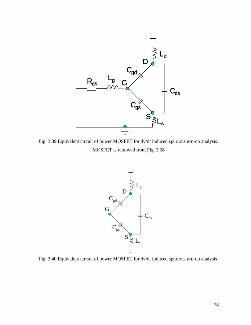
78
Cds
Cgd
Cgs
D
G
S
Rgs
Ls
Ld
Lg
Cds
Cgd
Cgs
D
G
S
Rgs
Ls
Ld
Cds
Cgd
Cgs
D
G
S
Rgs
Ls
Ld
Lg
Cds
Cgd
Cgs
D
G
S
Rgs
Ls
Ld
Fig. 3.39 Equivalent circuit of power MOSFET for dv/dt induced spurious urn-on analysis.
MOSFET is removed from Fig. 3.38
Cds
Cgd
Cgs
D
G
S Ls
Ld
Fig. 3.40 Equivalent circuit of power MOSFET for dv/dt induced spurious urn-on analysis.
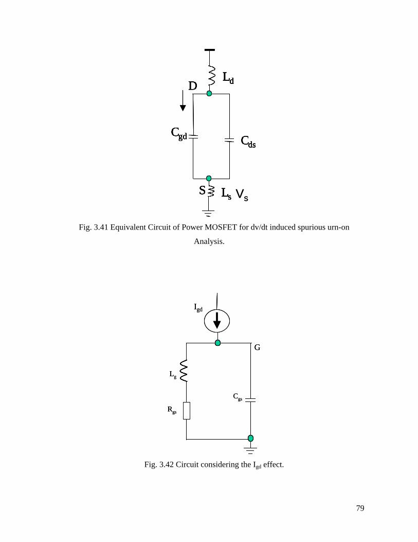
79
CdsCgd
D
S Ls
Ld
CdsCgd
D
S Ls
Ld
Vs
CdsCgd
D
S Ls
Ld
CdsCgd
D
S Ls
Ld
Ls
Ld
Vs
Fig. 3.41 Equivalent Circuit of Power MOSFET for dv/dt induced spurious urn-on
Analysis.
G
Cgs
Igd
Lg
Rgs
G
Cgs
Igd
Lg
Rgs
Fig. 3.42 Circuit considering the Igd effect.

80
Lg
G
Rgs
S
Cgs
Vgss
Lg
G
Rgs
S
Cgs
Vgss
Fig. 3.43 Circuit considering the Vgss effect.
-1
-0.5
0
0.5
1
1.5
2
2.5
0.0E+00 2.0E-09 4.0E-09 6.0E-09 8.0E-09 1.0E-08
Time (s)
Vol
tage
(V)
VgsVgsdcVgsacVgss
Fig. 3.44 An example of the analytical results.

81
00.5
11.5
22.5
33.5
44.5
0.0E+00 5.0E+08 1.0E+09 1.5E+09 2.0E+09
K(V/s)
Vmax
(V)
New model
Old model
Fig. 3.45 Comparison of Vmax between the new and old models.
0
0.5
1
1.5
2
2.5
0.0E+00 2.5E-09 5.0E-09 7.5E-09 1.0E-08
Time (s)
Vgs
(V)
Pspice SimulationAnalytical Model
Fig. 3.46 Comparison between analytical and simulation results.

0.4
0.8
1.2
1.6
2
0 5 10 15 20 25Normalized area of the MOSFET
Uni
t (V
)
Vmax
Fig. 3.47 Effect of the active area on the spurious turn-on voltage.
82

Chapter 4 FEA Analysis of the Power Loss of the Buck Converter
As addressed in the preceding chapter, the switching process of the buck converter is
inherently a nonlinear and high-order problem. In order to allow closed-form calculations, we
have to make several assumptions, which may lead to the considerable factors being ignored.
Actually, besides the switching loss of the high-side MOSFET, the spurious turn-on and the
body diode losses [B5]-[B10] are also very difficult to calculate using the traditional
approach. Although the circuit simulation can include all the parasitic, but the accuracy is still
limited by the analytical models [B27]-[B30].
FEA is a method of subdividing the problem into finite (smaller) elements. Using these
elements, the complex partial differential Equations that describe the behavior of a physical
structure can be reduced to a set of linear Equations that can easily be solved by the standard
techniques of matrix algebra.
The FEA is not a new method. In the late 1940s, the aerospace engineers began using FEA
as a structural analysis technique in aerospace design. From that time, thanks to the dramatic
increases in computer speed, the method has continually developed into a very sophisticated
generic tool, and is used in virtually every engineering discipline.
Although FEA has been widely used in the simulation of semiconductor devices, its
application in the DC/DC converter has not been explored due to the long simulation time and
the convergence problem. In this chapter, some approaches are proposed to reduce the
simulation time and overcome the non-convergence. Then, based on the FEA simulation
results, a detailed loss breakdown is performed. For the first time, the false-trigger-on loss is
extracted quantitatively. At the end of this chapter, the effects of both the device performance
and the parasitic elements on the power loss is studied extensively.
83
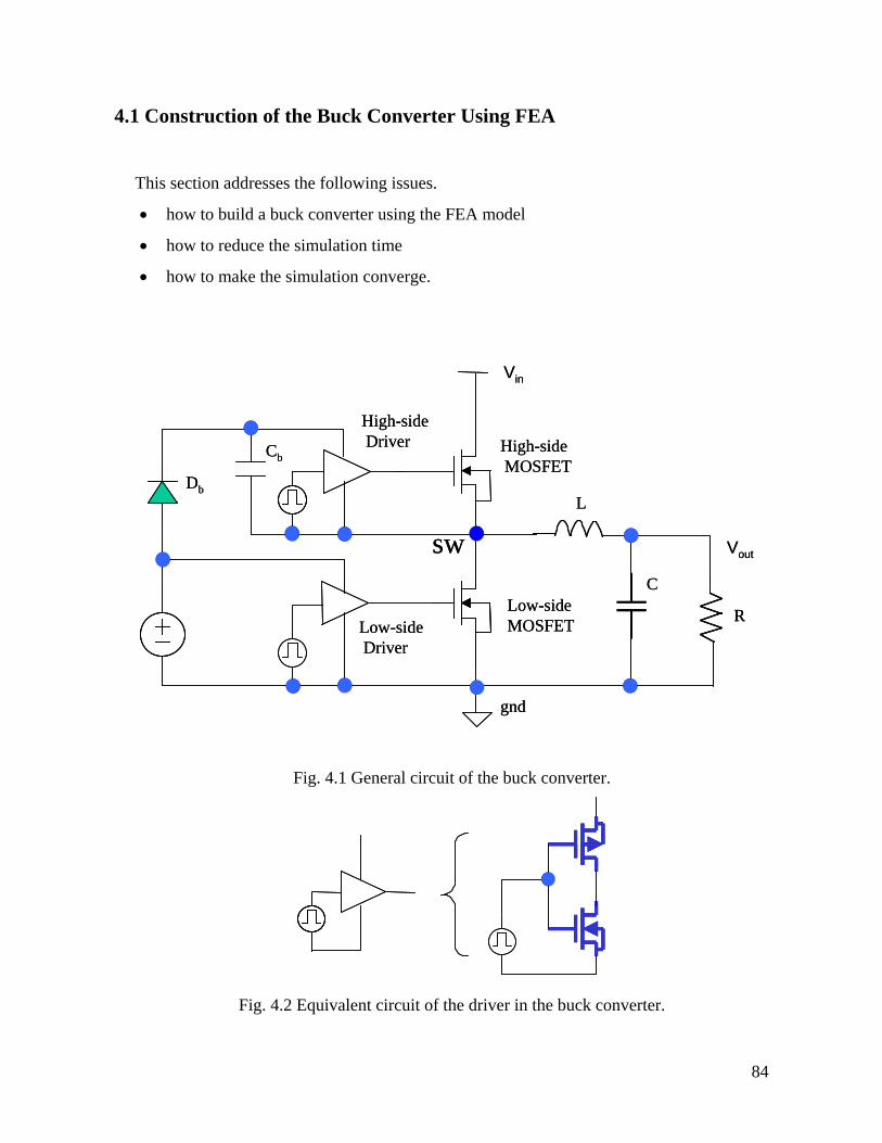
84
4.1 Construction of the Buck Converter Using FEA
This section addresses the following issues.
• how to build a buck converter using the FEA model
• how to reduce the simulation time
• how to make the simulation converge.
Vin
gnd
Vout
High-sideDriver
Low-sideDriver
High-sideMOSFET
Low-sideMOSFET
swL
C
R
Cb
Db
Vin
gnd
Vout
High-sideDriver
Low-sideDriver
High-sideMOSFET
Low-sideMOSFET
swL
C
R
Cb
Db
Fig. 4.1 General circuit of the buck converter.
Fig. 4.2 Equivalent circuit of the driver in the buck converter.

Rgh
i
Rgl
o
L ghi
L glo
L dhi
L dlo
L shi
L slo
Hi_
MO
S
Lo_M
OS
L b1 L b
2
Mph
i
Mpl
o
Mnh
i
Mnl
o
n 0
n 2n 3
n 32
n 7
n 9
n 10
n 12
n 11
n 13
n 14
n 15
n 16
n 17
n 18
n 19
Vin
Vdr
V drV
gl
Vgh
I o
Vhb
Vlb
Rsh
i
n 22
n 23
n 33
n 35
n 25
n 8 Rsl
oRdh
in 24
n 5n 6
n 34
Rb1 Rb2
n 36
RsaRsc
L sc
L sa
n 31
n 30
n 29
n 28
L b3
Rb3
n 1n 3
7n 3
9n 3
8
Rb5
L b5
Rb4
L b4
Fig. 4.3 Circuit used in the mixed-mode simulation.
4.1.1 Equivalent Circuit Used in the Simulation
The general circuit of the buck converter is shown in Fig. 4.1. In order to share the same
voltage source for the gate driver, Cb and Db comprise an auxiliary boot-strap circuit to power
the high-side driver.
85

86
The main components of the buck converter include the power MOSFET, the driver of the
power MOSFETs and the low-pass LC filter. Both the driver and the power MOSFETs are
semiconductor devices. However, we are going to use the Pspice instead of the FEA model to
describe the driver because of the following reasons.
• The switching speed of the CMOS driver is much faster than that of the power
MOSFET, and the effect of the driver’s switching process on the switching loss of the
power MOSFET is insignificant.
• Using the Pspice model can reduce the simulation time, since it is much simpler than
FEA.
Because the driver capability is determined by the last stage of the CMOS buffer, the
driver can be simplified as a CMOS inverter controlled by a pulse voltage source, as shown in
Fig. 4.2. The datasheet of the driver says that the output resistance of the NMOS and PMOS
of the inverter has a typical value of from 1 to 2 Ω.
There are two ways to build the FEA model for the power MOSFET, as follows.
• Using the process simulator (Tsuprem4): This method starts from a highly doped
silicon substrate, then an epitaxy of the drift layer is formed, and trench etching, gate
oxidation, implantation, diffusion and metallization follow to generate a power
MOSFET.
• Using the device simulator (Medici): This method directly defines the region of the
silicon, oxide and electrode as well as the doping profile of the P-body and the source.
For a general study of the power MOSFET’s switching, the second method is preferred,
because the process simulation is time consuming. However, for a specific design of the
MOSFET, the first method is necessary to determine the process parameters.
In principle, the simulation can be performed with mixed modeling, i.e., Pspice models are
used for the driver, and FEA models are used for the power MOSFET. Similar to the process
used for Pspice simulation, it is necessary to initialize both the voltage of each node and the
current of each circuit branch. However, when the FEA models connect with a non-zero
87
current inductor, the circuit usually does not converge at the beginning of the simulation. If
the current set through the inductor is zero, then it takes a lot of switching cycles for the
circuit to reach the steady state and the simulation time is too long. In order to eliminate the
transient process and guarantee that the simulation is convergent, the inductor must be
replaced by a current source. At the beginning of the simulation, both the voltage at any node
and the current through the current source are zero. Then, the voltages of the voltage source
and the current through the current source ramp up to the desired values in a short time (2 ns).
For example, the input voltage ramps up to 20 V, the driver voltage ramps up to 5 V, and the
current ramps up to 18 A. After this transient process, it is necessary to wait through another
period (1 µs) for the circuit to reach the steady state. After the circuit settles down, both the
high-side and low-side MOSFETs are off, and the current flows through the body diode of the
low-side MOSFET. If a Schottky diode is paralleled with the low-side MOSFET, most of the
current will go through the Schottky diode. Fig. 4.3 shows the equivalent circuit of the buck
converter used in the mixed-mode simulation. There are two points that should be noted, as
follows.
• The two parts of the boot-strap circuit (CBb B and DBb B) are replaced by a constant voltage
source (VBhiB) and a pulse voltage source (V BdhiB).
• The output capacitor is removed. Since a current source is used, the output capacitor
plays no role in the circuit. The output voltage of the buck converter is determined
using the principle of inductor volt-second balance, such that
∫=T
o dtVV0
10 (4.1)
where VB10B is the voltage of the node 10. The typical simulated waveforms of VBdslo B (VBds B of the
low-side MOSFET) and VBgslo B (VBgsB of the low-side MOSFET) are shown in Fig. 4.4.
4.1.2 Estimation of the Parasitic Inductance
In this section, the values of the parasitic inductance are estimated, based on the
calculation and simulation. There two kinds of parasitic inductance to be considered in the
simulation, as follows.

88
• The inductance of a single wire. This exists due to the bonding wired used in the
package.
• The inductance of a rectangular metal. This exits due to the metal trace of the PCB.
The self inductance of a single wire can be calculated using
]1)4[ln(2
0 −=dllLwr π
µ , (4.2)
where µB0B = 4π×10P
-9P H/cm is the permeability of the free space, l is the length of the wire, and
d is the diameter of the wire. As shown in Fig. 4.5, the self inductance of a single wire for the
SO8 package is between approximately 0.2 nH and 2.5 nH, depending on the length and
radius of the wire.
For the inductance of a rectangular metal, when the length (l) and width (w) are much
larger than the thickness (t), the self inductance is
]21)2[ln(
20 +=
wllLrct π
µ . (4.3)
Depending on the length and width of the rectangle, the typical value of the inductance is
between approximately 0.3 nH and 10 nH as shown in Fig. 4.6.
The assumption of Equation (4.3) is that the thickness of the rectangular metal is much less
than its length and width. This is true for the case of the PCB, because the typical thickness of
the PCB is between 33 µm and 132 µm.
Since the separations of the parasitic inductors are usually rather wide, the mutual
inductances between the inductors are ignored in the simulation of the buck converter.
The parasitic inductance can also be determined using commercial software such as
Maxwell. Fig. 4.7 shows the simulated inductance of the metal strip. Fig. 4.6 and Fig. 4.7
show sufficient agreement.

89
4.2 Using FEA to Extract Spurious Turn-on Loss
As discussed in Chapter 3, when the high-side MOSFET is turning on, the drain of the
low-side MOSFET experiences high dv/dt, which may trigger the low-side MOSFET to turn
on, thus causing more power loss. In this section, the process for extracting the spurious turn-
on loss is proposed, based on the mixed-mode simulation.
When the drain voltage of the low-side MOSFET is rising, besides the possible spurious
turn-on current, there are two other currents flowing the low-side MOSFET, as follows.
• The reverse-recovery current of the body diode,
• The displacement current that exists due to the charging of the output capacitance
(CBossB).
During the increase in drain voltage of the low-side MOSFET, the loss on the low-side
MOSFET can be expressed as
∫∫∫ ++=×== dtVIIIdtVIdtPE dsloqrrcsponlodslodlovrvr )( , (4.4)
where IBsponloB, I BcB and IBqrrB represent the current caused by spurious turn-on, CBoss B and the reverse
recovery of the body diode, respectively. The three components are separated in three steps,
as follows.
(1) When spurious turn-on occurs, there will be electron current (IBeslo B) flowing through the
channel and out of the source of the MOSFET. Fig. 4.8 and Fig. 4.9 compare the total current
and the electron current of the source with and without spurious turn-on, respectively. In Fig.
4.8, the electron current is only a small part of the total source current after the low-side
MOSFET recovers from reverse conduction. However, in Fig. 4.9, the electron current is a
dominant factor. Therefore, the power loss that occurs in the low-side MOSFET due to
spurious turn-on is
∫ ∫== dtVIdtVIE dsloeslodslosponlosponlo . (4.5)
Actually, IBsponloB also leads to more loss on the high-side MOSFET. This type of loss (EBsponhiB) is
a part of the turn-on loss of the high-side MOSFET, such that

90
∫ ∫== dtVIdtVIE dshieslodshisponlosponhi , (4.6)
where VBdshiB is the voltage between the drain and the source of the Hi-MOSFET.
(2) Because the energy stored in a capacitor depends on the voltage and is unrelated to the
charging process, the loss caused by CBoss B (EBcossB) can be found in another simulation by slowly
charging CBoss B to avoid spurious turn-on and reverse recovery, until the drain voltage reaches
VBin B. I BcossB also results in more loss in EBtonB. This part of the loss can be expressed as
sinossshi EVQE coscos −×= , (4.7)
where QBossB is the charge of CBoss B at the voltage of V Bin B.
(3) Finally, the loss due to the reverse recovery can be determined by
∫ −−== ssponlovrdsloqrrqrr EEEdtVIE cos . (4.8)
The total reverse-recovery charge is
osseslodlorr QdtIIQ ∫ −−= )( , (4.9)
and the loss on the high-side MOSFET due to QBrrB is
qrrinrrQrrhi EVQE −×= .
(4.10)
Usually, when finding the QBrrB in actual measurements, no distinction is made between QBrr B
and QBoss B. This will lead to significant error of QBrrB when it is much smaller than QBossB.
The key step in the separation of the three kinds of loss is that FEA can monitor the
electron current through the source. This is an important feature of the modeling.

91
Vgs
Vds
1us settle down
Vgs
Vds
1us settle down
Fig. 4.4 Simulated Vds and Vgs of the low-side MOSFET.
0
0.5
1
1.5
2
2.5
3
0 0.5 1 1.5 2 2.5 3Length of the wire (mm)
Indu
ctan
ce (n
H)
d=1mild=2mild=4mil
Fig. 4.5 Calculated inductance of a single wire.

92
0
2
4
6
8
10
12
14
0 5 10 15 20 25Length of the metal (mm)
Indu
ctan
ce (n
H)
W=2.5mmW=5mmW=10mm
Fig. 4.6 Calculated inductance of the metal strip.
0
2
4
6
8
10
12
14
0 5 10 15 20 25Lenght of the metal (mm)
Indu
ctan
ce (n
H)
W=2.5mmW=5mmW=10mm
Fig. 4.7 Simulated inductance of the metal strip.

93
Total current through the source of the low-side MOSFET (Islo)
Electron current through the sourceof the low-side MOSFET (Islo)
Total current through the source of the low-side MOSFET (Islo)
Electron current through the sourceof the low-side MOSFET (Islo)
Fig. 4.8 Current through the source of the low-side MOSFET without spurious turn-on.
Total current through the source of the low-side MOSFET (Islo)
Electron current through the sourceof the low-side MOSFET (Islo)
Total current through the source of the low-side MOSFET (Islo)
Electron current through the sourceof the low-side MOSFET (Islo)
Fig. 4.9 Current through the source of the low-side MOSFET with spurious turn-on.

94
4.3 Automated Analysis of Power Loss
So far, the power losses in the buck converter can be divided into four parts.
• The loss on the high-side MOSFET includes: turn-on loss, conduction loss, turn-off
loss, gate loss and package loss.
• The loss on the low-side MOSFET includes: conduction loss, deadtime loss, spurious
turn-on loss, QBrrB loss QBoss B loss, gate loss and package loss.
• The loss on the Schottky diode includes: conduction loss and package loss.
• The equivalent series resistance (ESR) loss of the inductor and the capacitor.
Although the mixed-mode simulation can be finished in less than half an hour, the
calculation of all these losses is not a trivial job. Therefore, a C program is built to
automatically perform the loss breakdown. This section defines of each kinds of loss and
describes how to use this program.
4.3.1 Critical Timings in the Simulation
In the automated power loss extraction program, the time boundary of conduction loss,
switching loss, deadtime loss etc. have to be defined mathematically, because, for example,
there is no abrupt switch between the turn-on loss and conduction loss of the high-side
MOSFET.
Before the simulation, the user must set some time parameters in the input simulation file
of Medici. The definitions of these time parameters are as follows.
• Period: The switching period of the buck converter.
• Ldelay: At Ldelay, the voltage source VBglB starts to drop and the low-side MOSFET
starts to turn on gradually. As explained in section 4.1.1, Ldelay is needed to settle
down the circuit. In the simulation file, TBglbenB is usually selected as 1 µs.
• Hon: During Hon, the pulse voltage V Bhb B keeps the voltage level at zero.

95
• Deadtime1 and Deadtime2. There are two deadtimes in one switching cycle. In this
dissertation, deadtime1 (the first deadtime) represents the deadtime after the low-side
MOSFET turns off and before the high-side MOSFET turn-on; deadtime2 (the second
deadtime) represents the deadtime after the high-side MOSFET turn-off and before the
low-side MOSFET turn-on.
Besides these basic timing parameters, the power loss extraction program uses the
simulation results to determine other timing variables. The definitions of these timing
variables are listed as follows.
• LBonB: The time period when the pulse voltage source V BglB keeps the voltage level low.
HonDeadtimeDeadtimePeriodLon −−−= 21 (4.11)
• TBbgnB: At TBbgn B, VBgsloB (VBgs B of the low-side MOSFET) rises up to 98% of VBdrB. TBbgn B is
defined as the beginning of the conduction of the low-side MOSFET.
• TBglendB: At TBglend B, the voltage source VBglB starts to drop, and the low-side MOSFET starts
to turn off gradually, such that
LonLdelayTglend += (4.12)
• TBcndlendB: At TBcndlendB, VBgslo B drops below 98% of VBdrB. TBcndlendB is defined as the end of the
conduction of the low-side MOSFET.
• TBdd1endB: At TBdd1endB, I BdlB (drain current of the low-side MOSFET) changes from negative
to positive. TBdd1endB is defined as the end of the first deadtime. The beginning of the first
deadtime is the end of the conduction of the low-side MOSFET (TBcndlendB).
• TBghbgnB: At TBghbgnB, the voltage source VBgh B starts to drop, and the high-side MOSFET
starts to turn on gradually.
• TBsponbgnB: At TBsponbgnB, the electron current through the source of the low-side MOSFET
changes from positive to negative. TBsponbgnB is used to determine the possible spurious
turn-on loss.
• TBcndhbgnB: At TBcndhbgnB, the instantaneous drain-to-source power loss of the high-side
MOSFET
dhidshidshi IVP ×= (4.13)

96
drops from the peak to the first valley. Tcndhbgn is defined as the end of the turn-on
period and the beginning of the conduction period of the high-side MOSFET.
• TBghendB: At TBghendB, the voltage source VBgh B starts to rise, and the high-side MOSFET starts
to turn off gradually, such that
HonVT ghbgnghend += (4.14)
• TBcndhendB: At TBcndhendB, VBgshiB (VBgsB of the high-side MOSFET) drops below 98% of VBdrB..
TBcndhendB is defined as the end of the conduction period and the beginning of the turn-off
period of the high-side MOSFET.
• TBdd2bgnB: At TBdd2bgnB, the instantaneous drain-to-source power loss of the low-side
MOSFET
dlodslodslo IVP ×= (4.15)
reaches the minimum value. TBdd2bgnB is defined as the beginning of the second
deadtime.
• TBend B: TBend B is defined as
PeriodTT bgnend += (4.16)
TBend B is the end of both deadtime2 and the power loss calculation.
4.3.2 Expressions of the Power loss
This section presents the strict definitions of various power losses in the buck converter
based on the timings described in the preceding section.
1) Power loss of the low-side MOSFET
• Conduction loss of the low-side MOSFET
∫ ×=Tcndlend
Tbgndlodslocndlo dtIV
PeriodP 1 (4.17)
• The first deadtime loss of the low-side MOSFET
∫ ×=endTdd
Tcndlenddlodslodd dtIV
PeriodP
1
11 (4.18)

97
• Power loss associated with the turn-on of the high-side MOSFET
∫ ×=Tghend
endTdddlodslovr dtIV
PeriodP
1
1 (4.19)
• Spurious turn-on loss
∫ ×=Ttghend
Tsponbgndloeslosponl dtIV
PeriodP 1 (4.20)
• Power loss associated with the turn-off of the high-side MOSFET
∫ ×=bgnTdd
Tghenddlodslovf dtIV
PeriodP
21 (4.21)
• The second deadtime loss of the low-side MOSFET
∫ ×=endTdd
Tdlodslodd
bgndd
dtIVPeriod
P2
2
2
1 (4.22)
• Gate loss of the low-side MOSFET
∫=Tglend
Ldelayglo
drglo dtI
PeriodVP , (4.23)
where IBglo B is the gate current of the low-side MOSFET.
Package loss of the low-side MOSFET
∫ ×+×=Tend
Tbgnslosldlodlpklo dtRIRI
PeriodP )(1 22 (4.24)
2) Power loss of the high-side MOSFET
• Turn-on loss of the high-side MOSFET
∫ ×=Tcndhbgn
Tglenddhidshitonhi dtIV
PeriodP 1 (4.25)
• Conduction loss of the high-side MOSFET

98
∫ ×=Tcndhend
Tcndhbgndhidshicndhi dtIV
PeriodP 1 (4.26)
• Turn-off loss of the high-side MOSFET
∫ ×=Tend
Tcndhenddhidshitofhi dtIV
PeriodP 1 (4.27)
• Gate loss of the high-side MOSFET
∫=Tglend
Ldelayghi
drghi dtI
PeriodVP (4.28)
• Package loss of the high-side MOSFET
∫ ×+×=Tend
Tbgnshishidhidhipkhi dtRIRI
PeriodP )(1 22 (4.29)
3) Power loss on the Schottky diode
The Schottky diode is an optional device in the buck converter. The power loss extraction
program can determine whether or not the Schottky diode is used in the simulation, and can
automatically calculate the power loss associated with the Schottky diode.
• The first deadtime loss of the Schottky diode
dtVIPTghend
TbgnAKAstkydd ∫ ×=1 , (4.30)
where IBAB is the anode current of the Schottky diode and VBAKB is the voltage between the
anode and the cathode of the Schottky diode.
• The second deadtime loss of the Schottky diode
dtVIPTend
TghendAKAstkydd ∫ ×=2 (4.31)
• Package loss of the Schottky diode

99
∫ +×=Tend
TbgnscsaApkstky dtRRI
PeriodP )(1 2
(4.32)
4) ESR loss of the inductor
Although in the simulation, the inductor is replaced by a current source, the ESR loss of
the inductor still can be determined by
∫ ×=Tend
Tbgnoesrl dtESRLI
PeriodP )(1 2 , (4.33)
where Io is the output current and ESRL is the ESR of the inductor.
5) ESR loss of the capacitor
Calculation of the ESR loss of the capacitor is based on the current ripple of the current
source, which can be approximated as
HonLVVI outin ⋅
−=∆
2, (4.34)
where L is the value of the inductor and Hon is defined in section 4.3.1. Therefore, the power
loss on the ESR of the capacitor is
3
])[(1 2
0
2 RIdtESRCtHon
IHon
PHon
esrc∆
=∆
= ∫ , (4.35)
where ESRC is the ESR of the capacitor.
5) Other resistive losses
The power loss of other parasitic resistors in Fig. 4.3 is determined by
∫ ×=Tend
Tbgnresres dtRI
PeriodP )(1 2 . (4.36)

100
4.3.3 Worked Example of the Program
The application of the power loss extraction program is rather simple. After the circuit
simulation, run the program in the same directory, for example
>sbc filename
where sbc is the name of the power loss extraction program and the filename is the input file
name for the circuit simulation. The analysis results will be displayed on the screen and also
be saved in the file named filename.rst under the current directory.
An example of the analysis result is shown in Fig. 4.10. There are eight sections in the
result. The first part shows the input voltage, output current and the output voltage of the buck
converter. The second part includes the voltage and current stress on the power MOSFETs.
The definitions of some symbols are given as follows
• VBsponB: the maximum spurious turn-on voltage across the gate and the source of the
low-side MOSFET.
• VBdsmaxhiB: the maximum voltage across the drain and the source of the high-side
MOSFET.
• VBdsmaxlo B: the maximum voltage across the drain and the source of the low-side
MOSFET.
• VBgsmaxhiB: the maximum voltage across the gate and the source of the high-side
MOSFET.
• VBgsminhiB: the minimum voltage across the gate and the source of the high-side
MOSFET.
• VBgsmaxlo B: the maximum voltage across the gate and the source of the low-side
MOSFET.
• VBgsminlo B: the minimum voltage across the gate and the source of the low-side
MOSFET.
• I BdmaxhiB: the maximum current through the drain of the high-side MOSFET.
• I Bdmaxlo B: the maximum current through the drain of the low-side MOSFET.
• I Bdminlo B: the minimum current through the drain of the low-side MOSFET.
• I BgmaxhiB: the maximum current through the gate of the high-side MOSFET.

101
• I BgminhiB: the minimum current through the gate of the high-side MOSFET.
• I Bgmaxlo B: the maximum current through the gate of the low-side MOSFET.
• I Bgminlo B: the minimum current through the gate of the low-side MOSFET.
The third part describes the power loss on the high-side MOSFET. The definitions of the
symbols are as follows.
• PBhiB: total power loss related to the high-side MOSFET.
pkhisihihi PPP += (4.37)
• PBsihiB: the sum of the switching loss and conduction loss of the high-side MOSFET
ghitofhicndhitonhisihi PPPPP +++= (4.38)
• PBswdshiB: the sum of the turn-on and the turn-off loss of the high-side MOSFET
tofhitonhiswdshi PPP += (4.39)
• PBswhiB: the total switching loss of the high-side MOSFET
ghiswdshiswhi PPP += (4.40)
• QBghiB: the total gate charge of the high-side MOSFET during the switching.
∫=Tglend
Ldelayghighi dtIQ (4.41)
The fourth part describes the power loss on the low-side MOSFET. The definitions of
some symbols are as follows
• PBlo B: total power loss related to the low-side MOSFET.
pklosilolo PPP += (4.42)
• PBsilo B: the sum of the switching loss and conduction loss of the low-side MOSFET
cndloswlosilo PPP += (4.43)
• PBswdslo B: the sum of PBvrB, PBdd1B, PBdd2 B and PBvfB.

102
vfddddvriswdslo PPPPP +++= 21 (4.44)
• PBswlo B: the total switching loss of the low-side MOSFET
gloswdsloswlo PPP += (4.45)
• QBglo B: the total gate charge of the low-side MOSFET during the switching.
∫=Tglend
Ldelaygloglo dtIP (4.46)
The fifth part describes the power loss on the low-side MOSFET. The definitions of some
symbols are as follows.
• PBstkyttB: total power loss related to the Schottky diode.
pkstkysistkystkytt PPP += (4.47)
• PBsistkyB: the sum of Pstkydd1 and Pstkydd2.
21 stkyddstkyddsistky PPP += (4.48)
The sixth part describes miscellaneous losses of the buck converter. The definitions of
some symbols are as follows.
• PBpcb B: the total loss associated with the parasitic resistance on the PCB.
])([15
254
24
23∫ ×+×+×=
Tend
Tbgnbbbbbsbpcb dtRIRIRI
PeriodP (4.49)
• PBsittB: is the sum of Psihi, Psilo and Psistky.
• PBotherB: is the power loss that cannot be determined by the circuit simulation, for
example, the magnetic loss of the inductor. The value of Pother is set in the input file.
The power loss extraction program reads Pother and uses it in the efficiency
calculation.
• PBttB: is the total power loss.
otherpcbesrcesrlstkyttlohitt PPPPPPPP ++++++= (4.50)

103
The seventh part describes the power loss associated with the spurious turn-on, CBoss B and
QBrrB, as addressed in section 4.2.
The eighth part shows the efficiency. The efficiency without gate loss is defined as
)( gloghittoutout
outoutng PPPVI
VI−−+⋅
⋅=η . (4.51)
The efficiency with the gate loss is defined as
ttoutout
outoutg PVI
VI+⋅
⋅=η . (4.52)
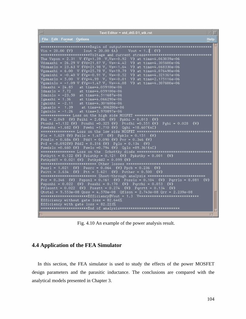
104
Fig. 4.10 An example of the power analysis result.
4.4 Application of the FEA Simulator
In this section, the FEA simulator is used to study the effects of the power MOSFET
design parameters and the parasitic inductance. The conclusions are compared with the
analytical models presented in Chapter 3.

105
4.4.1 Effect of the Design Parameters of the High-side MOSFET on
Efficiency
The major losses of the high-side MOSFET are those related to switching and conduction.
As addressed in Chapter 3, the switching loss is mainly determined by QBgd B, and the
conduction loss by RBds B. The effect of numerous design parameters on QBgdB, RBds B and the
efficiency are studied. In addition, the Figure of Merit (FOM = QBswB×RBds B) [B25] is also
investigated for each case in order to determine whether less FOM always results in higher
efficiency. In the following discussion, the operation condition of the buck converter is VBin B =
20V, I BoutB = 20A, and VBou Bt = 1.3V. 300KHz switching frequencies is used in the simulation.
(1) Trench width (WBtB)
The effects of WBtB on QBswB, RBds B and the FOM are shown in Fig. 4.11. Because WBtB introduces
CBgd B, larger WBtB results in more QBswB. On the other hand, wider WBtB reduces the RBdsB by enhancing
the spread of current under the trench. However, the FOM increases with WBtB. Fig. 4.12 shows
the simulated efficiency.
Conclusion 4.1: Less WBtB leads to higher efficiency, if the device area is chosen properly.
Obviously, the device area plays a very important role in efficiency. If the device area is
too small, the conduction loss will be very high; if the device area is too large, the switching
loss will be dominant. An optimized value for the area depends on the relative values of the
conduction and switching losses. For example, at a higher frequency (1 MHz), the optimized
area is less than at a low frequency (300 KHz). The reason is that the switching loss is
proportional to the switching frequency; the higher the frequency, the smaller the area needed
to reduce the switching loss. The optimized area also decreases with larger WBtB. This is also
because larger WBtB leads to more switching loss.
(2) Mesa width (WBmB)
The effects of WBmB on QBswB, RBds B and the FOM are shown in Fig. 4.13. Interestingly, the FOM
decreases with the increase of WBmB. The reason is that, for the fixed channel width (WBg B in
Equation (2.5)), the wider WBmB reduces the spreading resistance in the mesa region without

introducing much Qgd. In Fig. 4.13, the Rds increases with Wm because of the specific Rds is
used in the plot. Fig. 4.14 shows the simulated efficiency for different mesa widths.
Conclusion 4.2: Wider Wm leads to higher efficiency, if the device area is chosen
properly.
Although wider Wm results in higher efficiency, it negatively impacts the device area. For
example, at 300 KHz, the optimized area is about 10 mm2 for Wm = 2.5 um, while the
optimized area is about 4 mm2 for Wm = 1.0 um. The efficiency difference is less than 0.5%.
Therefore, the selection of Wm is a tradeoff between the cost and the performance.
(3) Thickness of the gate oxide (Tox)
The effects of Tox on Qsw, Rds and the FOM are shown in Fig. 4.15. As expected, thicker
Tox leads to higher Rds and lower Qsw. The overall effect is that the FOM decreases with the
increase of Tox. However, for Tox > 50 nm, the reduction of FOM is trivial. Fig. 4.16 shows
the effect of Tox on efficiency.
Conclusion 4.3: Thinner gate oxide leads to higher efficiency.
However, the gate oxide can be too thin, because it needs to support the gate-to-source
voltage. Typically, the minimum thickness of the gate oxide for such applications is about
30nm.
(4) The separation between the bottom of the trench and the bottom of the P-body (Ovp).
This parameter determines the Cgd of the trench sidewall. Less Ovp means less Cgd.
However, if Ovp is very small, the current spreading in the mesa region could be weakened
dramatically, which would results in huge Rds. Therefore, there is an optimized Ovp in terms
of FOM, as shown in Fig. 4.17. The negative Ovp in Fig. 4.17 means that the bottom of the P-
body is below the bottom of the gate trench. The effect of Ovp on the efficiency is shown in
Fig. 4.18. The optimized value of Ovp is zero. Therefore, we have the next conclusion:
Conclusion 4.4: the optimum design of the p-body depth is as close as possible to the
trench depth.
(5) The doping concentration of the drift region (N).
106

107
For a given breakdown voltage, the selection of doping concentration of the drift region
can span a wide range. As addressed in Chapter 3, the lightly doped N could lead to less QBgdB.
Fig. 4.19 shows the effects of N on QBswB, RBds B and the FOM for BV = 30 V. The lightly doped
drift region has less QBgd B, however, the increase of RBds B is more significant. Therefore, the non-
punch-through is a better design in terms of FOM. Fig. 4.20 shows that the non-punch-
through design not only has slightly higher efficiency, but also has less device area at the
optimized point.
Conclusion 4.5: Non-punch-through design is preferred for the optimized design.
(6) Effect of the breakdown voltage on efficiency.
Currently, most commercial MOSFETs for the application of the 20V input buck converter
have a breakdown voltage (BV) of 30V. Fig. 4.21 shows the effect of the BV on efficiency.
Actually, the performance of the low-breakdown (BV<30V) MOSFET is not as good as the
MOSFET with higher BV. This is because when the high-side MOSFET is turning off, the
parasitic inductances (LBdhiB and LBshiB) induce a voltage spike, which leads to extra loss on the
high-side MOSFET. Fig. 4.22 compares the turn-off losses of high-side MOSFETs with
different BV ratings. Apparently, the voltage spike is related to both the value of the parasitic
inductance (LBdhiB and LBshiB) and the turn-off speed of the high-side MOSFET. However, from 30
V to 35 V, the efficiency difference is less than 0.05%. Therefore, we have the following
conclusion.
Conclusion 4.6: For the high-side MOSFET, 30V voltage rating is a good choice for 20V
input buck converter.
(7) Effect of the threshold voltage the efficiency.
In the preceding simulations, all the threshold voltages of the high-side MOSFETs are
fixed at 1.7 V. However, the VBtB influences the power loss in three ways, as follows,
• Lower VBtB decreases the turn-on loss by introducing higher effective VBgs B = VBdrB -VBtB, if
the associated spurious turn-on loss is trivial.
• But lower VBtB also increases the turn-off loss by reducing the effective VBgsB = VBtB.
• Lower VBtB leads to less on-resistance of the MOSFET.

108
Actually, there must be an optimum VBtB for the high-side MSFET in terms of the power
loss, because of these facts.
• if Vt is close to 0, the MOSFET is very difficult to turn off. As a result, the turn-off
loss will be very large.
• if VBtB is close to VBdrB, the MOSFET is very difficult to turn on . Consequently, both the
turn-on and conduction losses will be very large.
Indeed, the optimum value of VBtB can be found by FEA simulation. As shown in Fig. 4.23,
the optimum VBtB is about 1 V. It should be noted that the optimum value of VBtB depends on
many conditions, for example, the switching frequency, the input and output voltage, etc.
Conclusion 4.7: There is an optimum VBtB of the hgih-side MOSFET
18
21
24
27
30
33
36
0.3 0.4 0.5 0.6 0.7
Trench width (um)
Rds
(moh
m.m
m2 ) o
r FO
M(n
C.m
ohm
)
120
130
140
150
160
170
180
Qsw
(nC
/cm
2 )
RdsFOMQsw
Fig. 4.11 Effects of trench width on the QBswB
, RBds B
and FOM.
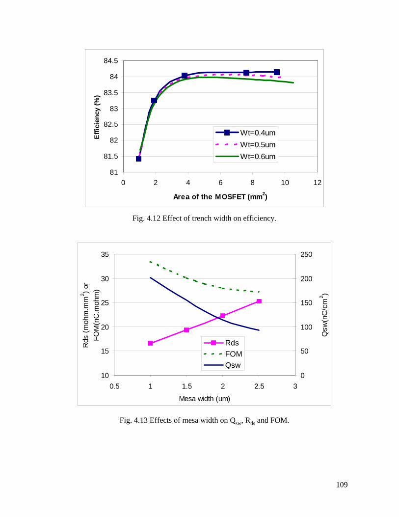
81
81.5
82
82.5
83
83.5
84
84.5
0 2 4 6 8 10
Area of the MOSFET (mm2)
Effi
cien
cy (%
)
12
Wt=0.4umWt=0.5umWt=0.6um
Fig. 4.12 Effect of trench width on efficiency.
10
15
20
25
30
35
0.5 1 1.5 2 2.5 3
Mesa width (um)
Rds
(moh
m.m
m2 ) o
r FO
M(n
C.m
ohm
)
0
50
100
150
200
250
Qsw
(nC
/cm
2 )
RdsFOMQsw
Fig. 4.13 Effects of mesa width on Qsw, Rds and FOM.
109

110
81
81.5
82
82.5
83
83.5
84
84.5
0 5 10 15 20
Area of the MOSFET (mm2)
Effi
cien
cy (%
)
Wm=1.0umWm=1.5umWm=2.0umWm=2.5um
Fig. 4.14 Effect of mesa width on efficiency.
15
17
19
21
23
25
27
29
31
0 20 40 60 80 100
Thickness of the gate oxide (nm)
Rds
(moh
m.m
m2 )
or
FOM
(nC
.moh
m)
20
40
60
80
100
120
140
160
180
Qsw
(nC
/cm
2 )
RdsFOMQsw
Fig. 4.15 Effects of the gate oxide thickness on QBgdB
, RBds B
and FOM.

111
79
80
81
82
83
84
85
0 5 10 15
Area of the MOSFET (mm2)
Effi
cien
cy (%
)
Tox=30nmTox=50nmTox=80nm
Fig. 4.16 Effect of the gate oxide thickness on efficiency.
15
20
25
30
35
40
-0.2 -0.1 0 0.1 0.2Ovp (um)
Rds
(moh
m.m
m2 ) o
r FO
M(n
C.m
ohm
)
130135140145150155160165170175180
Qsw
(nC
/cm
2 )RdsFOMQsw
Fig. 4.17 Effects of Ovp on Qgd, Rds and FOM.

112
79.580
80.581
81.582
82.583
83.584
84.5
0 5 10 15
Area of the MOSFET (mm2)
Effi
cien
cy (%
)
Ovp=-0.14umOvp=0umOvp=0.1um
Fig. 4.18 Effect of Ovp on efficiency.
10
15
20
25
30
35
40
45
5.0E+15 1.0E+16 1.5E+16 2.0E+16Doping concentration of the drift region(cm-3)
Rds
(moh
m.m
m2 ) o
r FO
M(n
C.m
ohm
)
135
140
145
150
155
160
165
170
Qsw
(nC
/cm
2 )
RdsFOMQsw
Fig. 4.19 Effects of the doping concentration of the drift region on QBgd B
, RBds B
and FOM.

113
79.580
80.581
81.582
82.583
83.584
84.5
0 2 4 6 8 10 12
Area of the MOSFET (mm2)
Effi
cien
cy (%
)
N=0.6e16N=1.0e16N=1.8e16
Fig. 4.20 Effect of the doping concentration of the drift region on the efficiency.
81
81.5
82
82.5
83
83.5
84
84.5
0 2 4 6 8 10 12
Area of the MOSFET (mm2)
Effi
cien
cy (%
)
BV=25VBV=35VBV=30V
Fig. 4.21 Effect of the breakdown voltage (BV) on efficiency.

114
Low BV MOSFET
High BV MOSFET
Breakdown ofthe body diode.
Low BV MOSFET
High BV MOSFET
Breakdown ofthe body diode.
Fig. 4.22 Turn-off waveforms of the high-side MOSFET.
80
81
82
83
84
85
0 2 4 6 8 10 12
Area of the MOSFET (mm2)
Effic
ienc
y (%
)
Vt=1.0VVt=1.7VVt=2.2VVt=0.7V
Fig. 4.23 Effect of VBtB on efficiency.

4.4.2 Effect of the Design Parameters of the Low-side MOSFET on
Efficiency
In this section, the effect of the design parameter of the low-side MOSFET on the
efficiency of the buck converter is investigated in the same manner as used in the preceding
section. Also, it is important to determine whether or not the FOM is a good index for the
low-side MOSFET from the efficiency standpoint
.
(1) Trench width (Wt)
Fig. 4.24 shows the effect of the trench width on efficiency. Although the conduction loss
is dominant in the power loss of the low-side MOSFET, if the device area of the low-side
MOSFET is too large, the efficiency drops. The reason is that a larger MOSFET has more
Cgd, and consequently is more prone to the spurious turn-on loss. This also explains the
advantage of a narrower trench width, which has less Cgd.
Conclusion 4.8: Less Wt leads to higher efficiency, if the device area is chosen properly.
(2) Mesa width (Wm)
Fig. 4.25 shows the effect of the mesa width on efficiency. At 300KHz switching
frequency, a wider trench width is preferred from the efficiency standpoint; at 1 MHz, a
narrow trench width is better. The less FOM of the wider Wm explains the simulation results
obtained at 300KHz. At higher frequencies, the loss of the output capacitance can be
substantial. Therefore, a narrow Wm is preferable.
Conclusion 4.9: Although there is an optimum value of Wm, less Wm is preferred in
terms of cost.
(3) Thickness of the gate oxide (Tox)
Because Tox impacts on-resistance, Cgd and Coss, it influences the tradeoff between the
conduction loss, spurious turn-on loss and the output capacitance loss. Fig. 4.26 shows that at
300 KHz, thinner Tox is preferred.
Conclusion 4.10: Thinner gate oxide leads to less power loss if the device area is chosen
properly.
115

116
(4) The separation between the bottom of the trench and the bottom of the P-body (Ovp).
Since a small Ovp can pinch off the current path under the gate trench, and a larger Ovp
results in more CBgdB, there is an optimum Ovp for the low-side MOSFET. Fig. 4.27 shows the
effects of Ovp on efficiency.
Conclusion 4.10: At 300 KHz, the optimum Ovp is about 0.
(5) The doping concentration of the drift region (N).
Fig. 4.28 shows that the non-punch-through design is better at 300 KHz.
Conclusion 4.11: The optimum doping concentration of the drift region depends on the
switching frequency.
(6) Effect of the BV on efficiency.
The low-side MOSFET experiences high voltage stress when the high-side MOSFET is
turning on. Such voltage stress determines the optimum voltage rating of the low-side
MOSFET. Fig. 4.29 shows the next conclusion.
Conclusion 4.12: For the low-side MOSFET, 30V voltage rating is a reasonable choice
for 20V input buck converter.
(7) Effect of the threshold voltage on the efficiency.
In the preceding simulations, all the threshold voltages of the low-side MOSFETs are fixed
at 1.7 V. However, the VBtB influences the power loss in the following two ways:
• Lower VBtB decreases the on-resistance of the MOSFET.
• Lower VBtB results in more spurious turn-on loss.
Actually, there must be a optimum VBtB for the low-side MSOFET in terms of the power loss,
because of the following evidence.
• if Vt is close to 0, the spurious turn-on loss can be significant.
• if Vt is close Vdr, the conduction loss of the low side MOSFET will be dominant.

As shown in Fig. 4.30, the optimum Vt of the low-side MOSFET is about 2 V. It should be
noted that the optimum value of Vt depends on many conditions, for example, the switching
frequency, the input and output voltage, etc.
Conclusion 4.13: There is an optimum Vt of the low-side MOSFET.
78
79
80
81
82
83
84
85
86
0 10 20 30 40
Area of the MOSFET (mm2)
Effic
ienc
y (%
)
Wt=0.4umWt=0.5umWt=0.6um
Fig. 4.24 Effect of trench width on efficiency.
117

118
81.5
82
82.5
83
83.5
84
84.5
85
0 10 20 30 40 50
Area of the MOSFET (mm2)
Effi
cien
cy (%
)
Wm=1.0umWm=1.5umWm=2.0um
Fig. 4.25 Effect of mesa width on efficiency.
81.5
82
82.5
83
83.5
84
84.5
85
0 20 40 60 80
Area of the MOSFET (mm2)
Effi
cien
cy (%
)
Tox=30nmTox=50nmTox=80nm
Fig. 4.26 Effect of the gate oxide thickness on efficiency.

8080.5
8181.5
8282.5
8383.5
8484.5
85
0 10 20 30
Area of the MOSFET (mm2)
Effic
ienc
y (%
)
40
Ovp=-0.14umOvp=0umOvp=0.1um
Fig. 4.27 Effect of Ovp on efficiency.
81
81.5
82
82.5
83
83.5
84
84.5
85
85.5
0 10 20 30
Area of the MOSFET (mm2)
Effi
cien
cy (%
)
40
N=0.6e16N=1.0e16N=1.8e16
Fig. 4.28 Effect of the doping concentration of the drift region on efficiency.
119
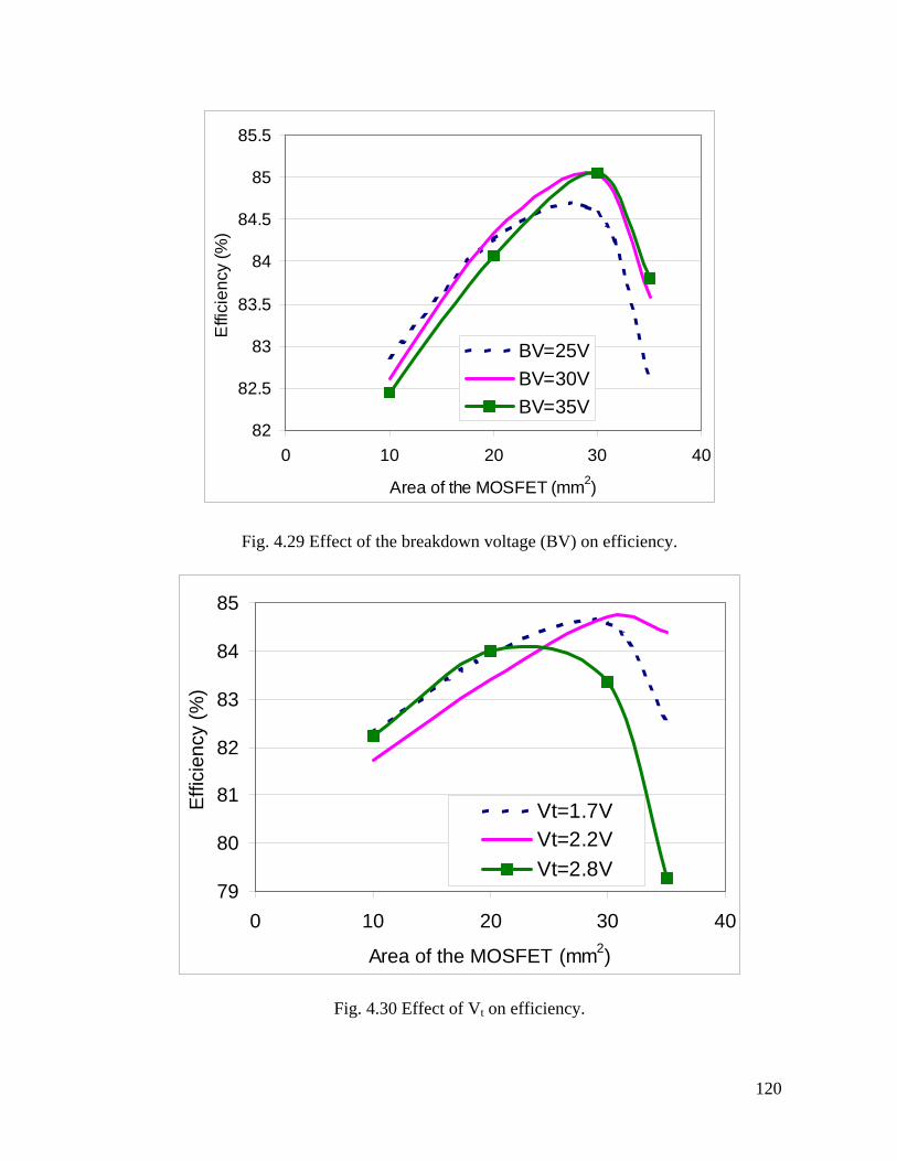
120
82
82.5
83
83.5
84
84.5
85
85.5
0 10 20 30 40
Area of the MOSFET (mm2)
Effi
cien
cy (%
)
BV=25VBV=30VBV=35V
Fig. 4.29 Effect of the breakdown voltage (BV) on efficiency.
79
80
81
82
83
84
85
0 10 20 30 40
Area of the MOSFET (mm2)
Effi
cien
cy (%
)
Vt=1.7VVt=2.2VVt=2.8V
Fig. 4.30 Effect of VBtB on efficiency.

121
4.4.3 Effect of the Parasitic Inductance on Efficiency
The effects of the parasitic inductances LBdhiB and LBshiB on the switching loss are addressed in
Chapter 3. In this section, such effects are quantified by FEA simulations.
(1) Effect of the LBdhiB on efficiency.
Fig. 4.31 shows the effect of LBdhiB on efficiency. In the practical range of L BdhiB, the variation
of the efficiency is very small. Therefore, less LBdhiB is preferred, because larger LBdhiB leads to
more voltage stress on the MOSFET, as shown in Fig. 4.32.
(2) Effect of the LBshiB on efficiency.
The impact of LBshiB on the switching process of the high-side MOSFET is addressed in
Chapter 3. Fig. 4.33 quantitatively demonstrated the conclusion that a larger LBshiB leads to more
switching loss and has significant effect on the efficiency.
81
81.5
82
82.5
83
83.5
84
84.5
0 5 10 15
Area of the MOSFET (mm2)
Effic
ienc
y (%
)
Ldhi=0.5nHLdhi=0.9nHLdhi=1.2nH
Fig. 4.31 Effect of LBdhiB
on efficiency.
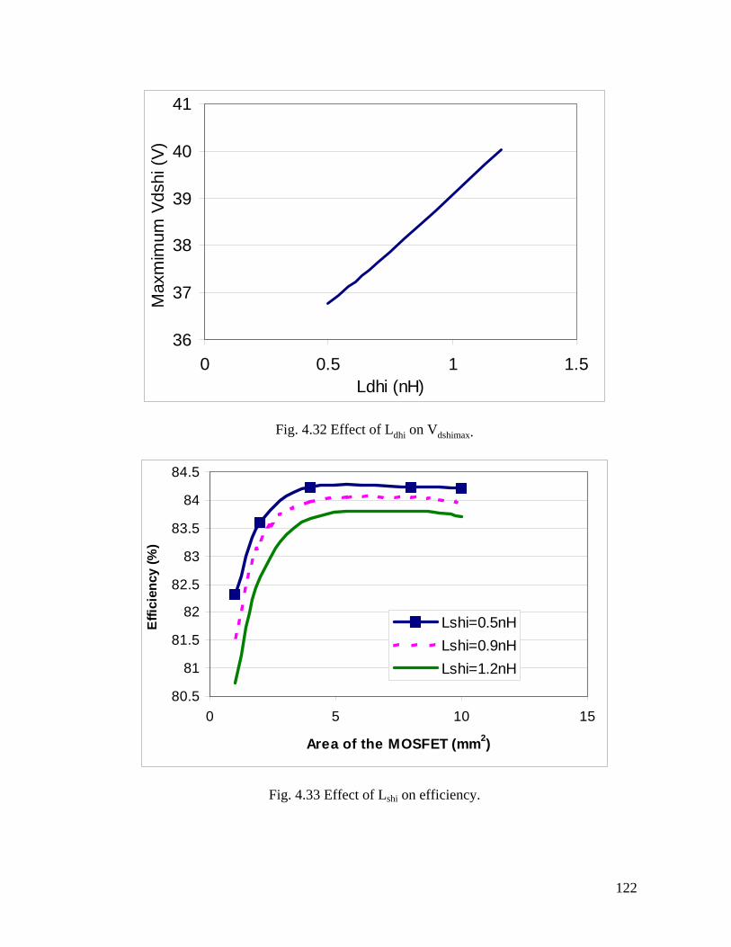
122
36
37
38
39
40
41
0 0.5 1 1.5Ldhi (nH)
Max
mim
um V
dshi
(V)
Fig. 4.32 Effect of LBdhiB
on VBdshimax B.
80.5
81
81.5
82
82.5
83
83.5
84
84.5
0 5 10 15
Area of the MOSFET (mm2)
Effic
ienc
y (%
)
Lshi=0.5nHLshi=0.9nHLshi=1.2nH
Fig. 4.33 Effect of Lshi on efficiency.
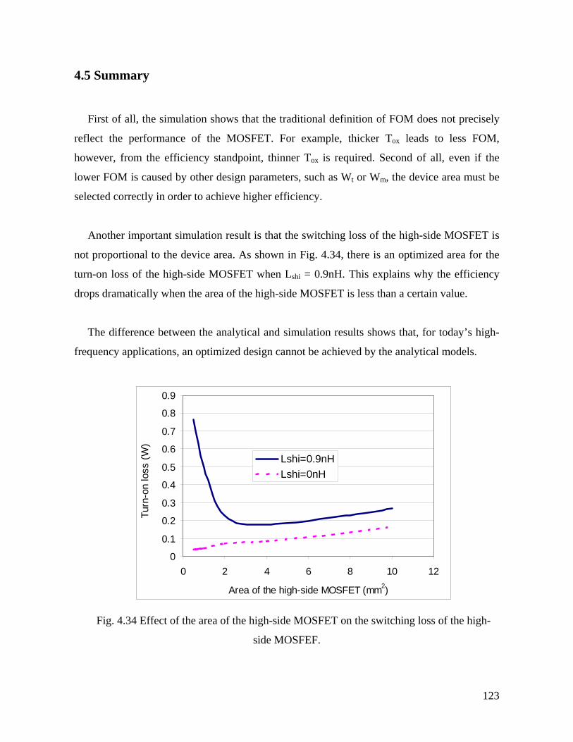
4.5 Summary
First of all, the simulation shows that the traditional definition of FOM does not precisely
reflect the performance of the MOSFET. For example, thicker Tox leads to less FOM,
however, from the efficiency standpoint, thinner Tox is required. Second of all, even if the
lower FOM is caused by other design parameters, such as Wt or Wm, the device area must be
selected correctly in order to achieve higher efficiency.
Another important simulation result is that the switching loss of the high-side MOSFET is
not proportional to the device area. As shown in Fig. 4.34, there is an optimized area for the
turn-on loss of the high-side MOSFET when Lshi = 0.9nH. This explains why the efficiency
drops dramatically when the area of the high-side MOSFET is less than a certain value.
The difference between the analytical and simulation results shows that, for today’s high-
frequency applications, an optimized design cannot be achieved by the analytical models.
0
0.1
0.2
0.3
0.4
0.5
0.6
0.7
0.8
0.9
0 2 4 6 8 10 12
Area of the high-side MOSFET (mm2)
Turn
-on
loss
(W)
Lshi=0.9nHLshi=0nH
Fig. 4.34 Effect of the area of the high-side MOSFET on the switching loss of the high-
side MOSFEF.
123

124
Chapter 5 Design of the Buck Converter Monolithically
5.1 Introduction
For the microprocessor, reducing the size of the power supply is very important, because
small size can decrease the parasitic elements, which degrade the performance of the power
supply. In order to minimize the effect of the parasitic elements, the power supply must be
arranged around the microprocessor. However, the estate of the motherboard is very
expensive. Therefore, smaller size is potentially more cost-effective from the system point of
view.
The major barrier for the small size power supply is the thermal issue, because smaller size
means poorer heat dissipation capability. If the temperature is very high, (the wildly accepted
temperature of the package case of the MOSFET is about 120°C.) the reliability of the power
system will be impaired. Currently, there are three types of power supply employed for the
microprocessor in terms of integration level.
• Discrete application. The power MOSFETs are packaged separately. For the desktop,
widely used package is DPAK or DDPAK; for the notebook, is SO8 or Power-PAK
SO8. The driver and controller are integrated monolithically or packaged individually.
• Co-package solution. The power MOSFET and the driver (controller) are packaged in
the same case.
• Monolithic integration. The power MOSFET and the diver (controller) are built on the
same silicon die.
In order to handle large current, the multi-phase topology is used. However, the more the
phase is, the more complex and expensive the power supply will be. Therefore, the number of
the phase tends to be as small as possible. Hence, high current capability of each phase is
preferred. The discrete application can handle more current, because the heat is dissipated by
much more package cases. Indeed, the discrete solution is dominant in the market [C5]-[C10]
now. However, as the switching frequency of the power supply keep increasing and the

125
parasitic elements of the package play more important role in the power loss, the co-package
and monolithic integration still have chance in the future [C11]-[C16]. With the advance of
the device technology and the performance of the lateral MOSFET [A19]-[A24], the current
capability of the monolithic solution increases steadily.
The basic function blocks in the monolithic integrated buck converter are illustrated in Fig.
5.1. The high voltage part includes the power MOSFET and the lever shift circuit; the low
voltage part includes the deadtime generation and the switching control. In this chapter, an
economical 5V/12V process is demonstrated. Then, a monolithic design is presented.
5.2 Process Design
Although the UMOSFET has larger current capability than the LDMOS, UMOSFETs can
not be integrated monolithically in the buck converter, because of the following facts.
• In the buck converter, the source of the high-side MOSFET is connected with the
drain of the low-side MOSFET. However, in the monolithic integration, the drains of
UMOSFETs are tied together, because all the UMOSFETs share the same substrate.
• The substrate of the main stream CMOS process is of p-type. It is not suitable for the
integration of the N-type UMOSFET.
In this section, an economical 5V/12V process is presented, which uses only two masks in
addition to standard p-well technology. This process features a broad range of MOSFET and
bipolar devices integrated on a common p-type substrate, including 5V CMOS, LDNMOS,
LDPMOS, LIGBT and bipolar transistors. The self-isolation approach on p-type substrate
allows the integration of the low voltage circuit, bootstrap circuit, low-side switch and high-
side switch monolithically.
5.2.1 Process Flow

126
For the 12V VRM application, the voltage rating of the power MOSFET should be about
20V, which can be realized in several processes. However, most of these processes are very
complicated or don’t provide fully isolation between high-side and low-side MOSFETs.
Hence, we developed a cost-effective CMOS-compatible technology, which has been
demonstrated in Cornell Nanofabrication Facility (CNF).
The basic problem should be solved in the monolithic integration is how to isolate the low
voltage MOSFET from the high voltage MOSFET. Fig. 5.2 shows device structure of
different function blocks. The low voltage CMOS circuit feeds switching signals to the gate of
the low-side MOSFET and to the input of the level shift circuit, which passes the signal to the
driver of the high-side MOSFET. Except the block of the CMOS circuit, all MOSFET
employs the lateral power MOSFET to realize the isolation.
The process starts on a 100~200 Ω⋅cm p-type substrate. The key process steps are as
follows.
(1) Property of the silicon: P type <100>, 500-550 µm, 100-200 Ω.cm.
(2) Screen oxidation 50nm. Diffusion time = 30 min, Temperature = 1050 °C.
(3) Phosphor implantation. The implantation parameters are determined by the threshold
voltage of the low voltage PMOS. Dose = 1.3×10P
12P, Energy = 50 kev.
(4) Boron implantation. The implantation parameters are determined by the threshold voltage
of the low voltage NMOS (Fig. 5.3). Dose = 1.3×10P
13P, Energy = 50 kev.
(5) P-well alignment etching. Etching oxide 20 nm for the alignment of the active region in
the next step. Remove photo resist.
(6) Diffusion (Fig. 5.4). Time = 685 min, Temperature = 1150 °C.
(7) Deposition of 12 nm nitride for the field oxidation.
(8) Etching off the nitride from the inactive area (Fig. 5.5).
(9) 0.94 µm field oxidation (Fig. 5.6). Time = 80 min, Temperature = 1150 °C.
(10) 35 nm gate oxidation.
(11) Poly gate definition (Fig. 5.7).
(12) Boron implantation for the P-body of the LDMOS (Fig. 5.8). Dose = 2.5×10P
13P, Energy =
30 kev.

127
(13) Phosphor implantation for the N-region of the LDMOS (Fig. 5.9). Dose = 1.0×10P
13P,
Energy = 20 kev.
(14) Diffusion (Fig. 5.10). Time = 35 min, Temperature = 1150 °C.
(15) Boron implantation for the PP
+P contact (Fig. 5.11). Dose = 2.0×10P
15P, Energy = 10 kev.
(16) Phosphor implantation for the NP
+P contact (Fig. 5.12). Dose = 4.0×10P
15P, Energy = 20 kev.
(17) Fast anneal (Fig. 5.13). Time = 0.5 min, Temperature = 920 °C.
Compared with standard p-well CMOS process, only two masks (p-body and n-regrion)
are added. There are totally ten masks used in the process:
(1) Pwell layer. In step 4 to define the region of P-well.
(2) Active layer. In step 8 to define the active region.
(3) Gatepoly layer. In step 11 to define the poly gate.
(4) Pbody layer. In step 12 to define the P-body of the LDMOS.
(5) Nregion layer. In step 13 to define the N-region of the LDMOS.
(6) Pplus layer. In step 15 to define the PP
+P region.
(7) Nplus layer. In step 16 to define the N P
+P region.
(8) Contact layer.
(9) Metal layer.
(10) Passivation layer.
This work was performed at the Cornell Nanofabrication Facility (a member of the
National Nanofabrication Users Network). The top view of a fabricated LDMOS and the
SEM picture of the poly gate are shown in Fig. 5.14.

128
Level shift
Deadtime generation
Switchingcontrol
Level shift
generation
12 V12 V
Switchingcontrol
HV MOSFET
HV
MO
SFET
Level shift
Deadtime generation
Switchingcontrol
Level shift
generation
12 V12 V
Switchingcontrol
HV MOSFET
HV
MO
SFET
Fig. 5.1 Topology of monolithically integrated buck converter.
12 V
-0.7~12.7 V
N+P+ N+p
Psub
5V
P+ N+P+N
4.3~16.3V
P+ N+P+
N
Low side LDMOS
CMOS Circuit
High side LDMOS
Level shift
4.3~16.3 V
Charge pump and high Side LDMOS driver
-0.7~12.7 V
Psub
N+P+N+
p
P subN
N+P+N+
p
P subN
N+P+N+
p
P subN
P sub
N+P+N+
p
P subN
12 V
-0.7~12.7 V
N+P+ N+p
Psub
5V
P+ N+P+N
4.3~16.3V
P+ N+P+
N
Low side LDMOS
CMOS Circuit
High side LDMOS
Level shift
4.3~16.3 V
Charge pump and high Side LDMOS driver
-0.7~12.7 V
Psub
N+P+N+
p
P subN
N+P+N+
p
P subN
N+P+N+
p
P subN
N+P+N+
p
P subN
N+P+N+
p
P subN
P sub
N+P+N+
p
P subN
Fig. 5.2 Isolation and signal flow in the monolithically integrated buck converter.

129
Boron implantation
Photo resist
Phosphor
Silicon
Boron implantation
Photo resist
Phosphor
Silicon
Fig. 5.3 Simulated cross section of the process flow (Step 4).
N-well P-wellN-well P-well
Fig. 5.4 Simulated cross section of the process flow (Step 6).
Nitride Photo resistNitride Photo resist
Fig. 5.5 Simulated cross section of the process flow (Step 8).

130
Field oxideField oxide
Fig. 5.6 Simulated cross section of the process flow (Step 9).
Poly gate of low voltage PMOSPoly gate of low voltage NMOSPoly gate of LDMOS Poly gate of low voltage PMOSPoly gate of low voltage NMOSPoly gate of LDMOS
Fig. 5.7 Simulated cross section of the process flow (Step 11).
Boron implantation
Photo resist
P-body of LDMOS
Boron implantation
Photo resist
P-body of LDMOS
Fig. 5.8 Simulated cross section of the process flow (Step 12).

131
Phosphor implantation
Photo resistN-region of LDMOS
Phosphor implantation
Photo resistN-region of LDMOS
Fig. 5.9 Simulated cross section of the process flow (Step 13).
LDMOS Field oxide Low voltage NMOS Low voltage PMOSLDMOS Field oxide Low voltage NMOS Low voltage PMOS
Fig. 5.10 Simulated cross section of the process flow (Step 14).
Boron implantation
Photo resist
Boron implantation
Photo resist
Fig. 5.11 Simulated cross section of the process flow (Step 15).
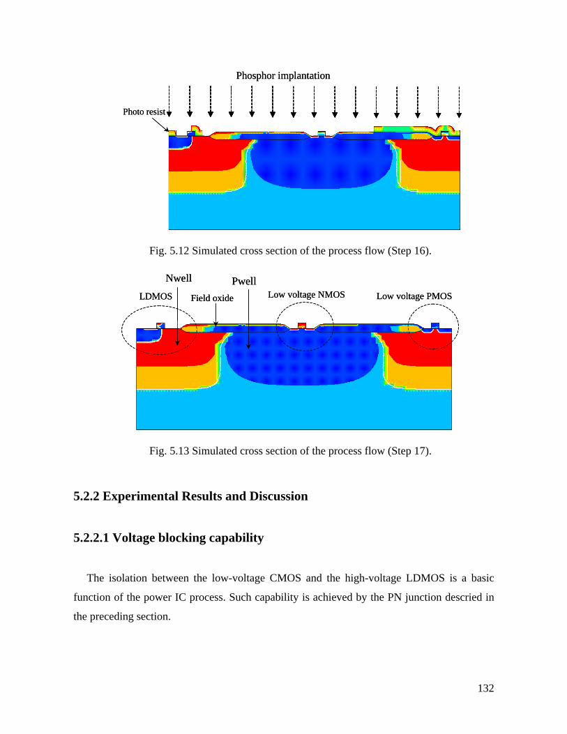
132
Phosphor implantation
Photo resist
Phosphor implantation
Photo resist
Fig. 5.12 Simulated cross section of the process flow (Step 16).
LDMOS Field oxide Low voltage NMOS Low voltage PMOS
Nwell PwellLDMOS Field oxide Low voltage NMOS Low voltage PMOS
Nwell Pwell
Fig. 5.13 Simulated cross section of the process flow (Step 17).
5.2.2 Experimental Results and Discussion
5.2.2.1 Voltage blocking capability
The isolation between the low-voltage CMOS and the high-voltage LDMOS is a basic
function of the power IC process. Such capability is achieved by the PN junction descried in
the preceding section.

133
Fig. 5.15 shows the breakdown characteristic between the N-well and the P-well. The
breakdown voltage is above 140 V. Because the LDMOS is located in the N-well, this means
the isolation voltage between the LDMOS and the CMOS can be as high as 140V. Such
voltage is enough for the 20 V input buck converter.
Fig. 5.16 shows breakdown characteristic between the N-well and the P-body of the
LDMOS. The breakdown voltage is above 43 V. This is the maximum voltage rating of the
LDMOS. It also meets the design target.
5.2.2.2 Performance of the MOSFETs
The structure and the forward conduction characteristics of the PMOS and NMOS are
shown in Fig. 5.17 and Fig. 5.18 respectively. Both NMOS and PMOS demonstrate good
performance, which is suitable for 5V application.
Fig. 5.19 shows the structure and the characteristic of the LDMOS. The breakdown voltage
of the LDMOS is about 18V. Table 5.1 compares the experimental and simulation results of
the MOSFETs. The difference between the simulation and experiment is reasonable, because
the contamination in the process is almost inevitable.
Table 5.1 Comparison of the experimental and simulation
results
8.76.8 (simulation)
1820 (simulation)
1.41.3 (simulation)
LDMOSLg = 0.8 µmLd = 0.8 µm
2018 (simulation)
16 13 (simulation)
0.8 0.9 (simulation)
PMOSLg = 0.8 µm
75 (simulation)
12 13 (simulation)
0.6 0.7 (simulation)
NMOS Lg = 0.8 µm
Ron (kΩ•µm)BV (V)Vt (V)
8.76.8 (simulation)
1820 (simulation)
1.41.3 (simulation)
LDMOSLg = 0.8 µmLd = 0.8 µm
2018 (simulation)
16 13 (simulation)
0.8 0.9 (simulation)
PMOSLg = 0.8 µm
75 (simulation)
12 13 (simulation)
0.6 0.7 (simulation)
NMOS Lg = 0.8 µm
Ron (kΩ•µm)BV (V)Vt (V)

134
Besides the voltage blocking capability and the performance of the MOSFETs, the
characteristics of the inverter is also tested. Fig. 5.20 illustrates the DC transfer characteristic
of a single stage inverter, the AC gain of which is pretty high.
The experimental results demonstrate the proposed process has enough isolation capability
for the monolithic integration of 12V input buck converter, the characteristics of the
MOSFETs are close to the simulation results and the performance of the inverter is good. The
whole circuit of the buck converter is not built up based on this process, because the
fabrication facility is not suitable for the large area device. However, the monolithic
integration is performed using another process developed in the National Semiconductor
Company as discussed in the next section.
23,400 times SEM pictureof the 0.8 µm gateTop view of a LDMOS
Drain
Gate Source
23,400 times SEM pictureof the 0.8 µm gateTop view of a LDMOS
Drain
Gate Source
Fig. 5.14 Pictures of the fabricated device structure

135
P-sub
N-well P-well
Vmax = 140 V
-2.0E-04
-1.0E-04
0.0E+00
1.0E-04
2.0E-04
3.0E-04
4.0E-04
5.0E-04
-200 -150 -100 -50 0 50
Voltage between P well and N well (V)
Cur
rent
from
P w
ell t
o N
wel
l (A)
P-sub
N-well P-well
Vmax = 140 V
-2.0E-04
-1.0E-04
0.0E+00
1.0E-04
2.0E-04
3.0E-04
4.0E-04
5.0E-04
-200 -150 -100 -50 0 50
Voltage between P well and N well (V)
Cur
rent
from
P w
ell t
o N
wel
l (A)
Fig. 5.15 Experiment results of the breakdown characteristic between the P-well and N-
well.
P-bodyN+P+
P-sub
N-well
Vmax = 43 V
-2.0E-04
-1.0E-04
0.0E+00
1.0E-04
2.0E-04
3.0E-04
4.0E-04
5.0E-04
6.0E-04
-50 -40 -30 -20 -10 0 10
Voltage (V)
Curr
ent (
A)
PN breakdown between P body and NwellP-body
N+P+
P-sub
N-well
Vmax = 43 V
-2.0E-04
-1.0E-04
0.0E+00
1.0E-04
2.0E-04
3.0E-04
4.0E-04
5.0E-04
6.0E-04
-50 -40 -30 -20 -10 0 10
Voltage (V)
Curr
ent (
A)
PN breakdown between P body and Nwell
Fig. 5.16 Experiment results of the breakdown characteristic between the P-body and N-
well.

136
N+
P-sub 1e15
N+
P-well
Lg
Wg
P+
0
1
2
3
4
5
6
7
0 2 4 6 8 10
Vds (V)
Ids
(mA
)
Vg = 0 ~ 5 V
Lg= 1.2 µm Wg = 40 µm
N+
P-sub 1e15
N+
P-well
Lg
Wg
P+
0
1
2
3
4
5
6
7
0 2 4 6 8 10
Vds (V)
Ids
(mA
)
Vg = 0 ~ 5 V
Lg= 1.2 µm Wg = 40 µm
Fig. 5.17 Experiment results of the forward conduction characteristic of the low-voltage
NMOS.
0
0.5
1
1.5
2
2.5
0 2 4 6 8 10
Vds (V)
Ids
(mA
)
P+
P-sub 1e15
P+
N-well
Lg
Wg
N+
Lg= 1.2 µm Wg = 40 µm
0
0.5
1
1.5
2
2.5
0 2 4 6 8 10
Vds (V)
Ids
(mA
)
P+
P-sub 1e15
P+
N-well
Lg
Wg
N+
Lg= 1.2 µm Wg = 40 µm
Fig. 5.18 Experiment results of the forward conduction characteristic of the low-voltage
PMOS.

137
P-bodyN+P+
P-sub 1e15
NN+
N-well 2e16
Ln
Wg
Lg= 1.2 µmLn = 0.8 µmWg = 40 µm
0
4
8
12
16
0 5 10 15 20
Vds (V)
Ids
(mA
)
Vg=0 ~3 V
0
0.5
1
1.5
2
2.5
3
0 0.02 0.04 0.06 0.08 0.1
Vds (V)
Ids
(mA)
P-bodyN+P+
P-sub 1e15
NN+
N-well 2e16
Ln
Wg
Lg= 1.2 µmLn = 0.8 µmWg = 40 µm
0
4
8
12
16
0 5 10 15 20
Vds (V)
Ids
(mA
)
Vg=0 ~3 V
0
0.5
1
1.5
2
2.5
3
0 0.02 0.04 0.06 0.08 0.1
Vds (V)
Ids
(mA)
Fig. 5.19 Experiment results of the forward conduction characteristic of the LDMOS
0
1
2
3
4
5
0 1 2 3 4 5
Vin (V)
Vout
(V) Inv
Vin Vout
PMOS
NMOS
0
1
2
3
4
5
0 1 2 3 4 5
Vin (V)
Vout
(V) Inv
Vin Vout
PMOS
NMOS
Fig. 5.20 DC transfer characteristic of the inverter.

138
5.3 Monolithic Design of the Buck Converter
This section presents a monolithic design of the buck converter, which employs National
Semiconductor’s power IC process. In this process, the isolation is realized by deep trench
filled by polysilicon. The typical devices of this process includes
• Vertical NPN and PNP bipolar transistor,
• 30V N-type LDMOS,
• Low voltage PMOS and NMOS,
• High voltage PMOS and NMOS,
• Zener diode.
5.3.1 Design of the LDMOS
The main design challenge of the monolithic integration of the high voltage LDMOS is
that the on resistance of LDMOS is much larger than that of the power UMOSFET, because
of the following facts.
• As addressed in the section (2.1.2), the specific on resistance (resistance per unit area)
of LDMOS is inherently larger than that of the UMOSFET. The typical specific on
resistance of the 30 V LDMOS is about 40 mΩ·cmP
2P, while it is below 30 mΩ·cmP
2P for
the 30 V UMOSFET.
• It is impractical to reduce the resistance of the LDMOS by increasing the device area,
because the metal debiasing effect can significantly increase the total resistance when
the device area is large and the maximum the device area is limited by the package.
Since the main current path of the LDMOS is from the drain to the source and the source
of high-side MOSFET is connected with drain of the low-side MOSFET, the shape of the
layout of both the high-side and low-side MOSFET is flat as shown in Fig. 5.21. In order to
handle large current, three pins are dedicated for the drain of the high-side MOSFET and
source of the low-side MOSFET, for pins for the switching node. One problem associated
with such flat design of the power MOSFET is that the connection between the last stage of

139
the driver to the gate of the power MOSFET is very long. The parasitic resistance and
inductance of the long connection path can slow down the switching speed of the MOSFET.
This effect is more significant for the low-side MOSFET, since it has more gate charge than
the high-side MOSFET. Therefore, the last stage of the gate driver is designed like a narrow
bar and located by the side of the low-side MOSFET to accelerate the switching of the low-
side MOSFET (Fig. 5.22).
The final selection of the area of the MOSFET depends on the optimization results. Since
the process is fixed, the only parameter can be tuned is the area of the MOSFET. The
simulated efficiency as the function of the MOSFET area is shown in Fig. 5.23. The
simulation condition is
• input voltage is 12 V,
• output voltage is 1.7 V,
• output current is 4 A,
• switching frequency is 1MHz.
Based on Fig. 5.22, the area of the low-side MOSFET is 2.535mmP
2P, the area of the high-
side MOSFET is 1.211mmP
2P. Fig. 5.23 shows the overall design. The adaptive deadtime
control is addressed in the next section.
5.3.2 Adaptive Deadtime Control of the Buck Converter
As described in Chapter 4, the power loss due to the deadtime (deadtime loss) is not trivial
in the buck converter. In the duration of the deadtime, the current goes through the body diode
of the low-side MOSFEF, resulting in instantaneous high power loss, because the forward
voltage drop of the body diode (typically is 0.7V) is much larger than the voltage drop of the
MOSFET (typically is 0.05 V). Another loss associated with the conduction of the body diode
is the reverse recovery loss. Therefore, reducing the deadtime can substantially decrease the
power loss especially at high switching frequency. Usually the deadtime is fixed and
determined by the driver/controller. The duration of the deadtime can’t be designed too short.
Otherwise, it may cause the turn-on of both the high-side and low-side MOSFETs. The basic

idea of the adaptive deadtime control is to sense the turn-on of the body diode. Upon sensing
the turn-on, the voltage sensor triggers a gate controller to turn on a switch in the regulator,
and thereby terminate a dead time. The voltage sensor and gate controller are high-speed
circuits, and therefore can reduce the duration of the dead time. Reducing the dead time
duration improves efficiency by reducing the duration of body diode conduction. The dead
time can be reduced to less than a turn-on time of the body diode, thereby preventing charge
buildup in the body diode, and consequently preventing reverse recovery loss in the body
diode.
Sensing the high-side MOSFET turn off (deadtime2) will typically be an easier task than
sensing the low-side MOSFET turn off (deadtime1). This is because Vsw (Fig. 5.23) has a
relatively large change from Vin to about -0.7 volts when the high-side MOSFET is turn-off,
and Vsw has a relatively small change from about zero volts to about -0.7 volts when the low-
side MOSFET is turning off. Therefore, the voltage sensor must be able to sense small, rapid
voltage changes, and produce a trigger for the gate controller in response. In addition, the
voltage sensor must be capable of withstanding without damage relatively high voltage spikes
in Vsw. Preferably, the voltage sensor can respond to a change in the swing node voltage from
-0.1 to -0.3 volts in about 1 nanosecond.
Several circuits can be used as the voltage sensor, including high speed voltage amplifiers,
high speed voltage comparators, and the like. The voltage sensor must have high sensitivity to
voltage reversals, high speed, and a tolerance for high peak voltages.
Fig. 5.24 shows a specific embodiment of the present invention where the voltage sensor is
an NPN bipolar transistor with an emitter E connected to the swing node. The transistor has a
base B connected to ground potential, or to a potential in the range of about zero to +0.6 volts.
The collector C is connected to the switching control. A resistor R is connected to the
collector C and a voltage source (+5V) providing, for example, a digital signal level voltage
(e.g. 5 volts). The resistance of resistor R is selected so that voltage at collector C drops to
about zero and switching control receives triggers when the deadtime occur. An appropriate
140

141
resistance value for resistor R can be, for example about 50 kΩ to 250 kΩ. The gain of the
transistor can have a wide ranging value, for example in the range of about 10-100.
In operation, transistor is off while the high-side MOSFET or the low-side MOSFET is on.
Transistor turns on at the deadtime, when the swing node voltage VBswB falls below
approximately ground potential. At this time, the transistor triggers the switching control by
low voltage level. The switching control in response turns on the high-side MOSFET or the
low-side MOSFET, depending on which deadtime has just occurred.
It is noted that the speed and sensitivity of the bipolar transistor can be improved by
connecting the base B to a slightly positive voltage in the range of about 0 to + 0.6 volts. Such
a slightly positive voltage tends to cause the bipolar transistor to turn on sooner, thereby
allowing for shorter dead times. However, it is noted that if the base voltage is too high (e.g. 1
volt), false triggering of the gate controller will result.
Also, it is important for transistor to be able to withstand without damage the high voltage
spike that occurs at the swing node. This voltage spike is applied across the emitter-base
junction, which is often an easily damaged junction in bipolar transistors. A particularly
useful bipolar transistor for is a parasitic bipolar transistor integral to the power LDMOS. The
parasitic bipolar transistor integral to an LDMOSFET shown in Fig. 5.24 has high emitter-
base voltage capability (due to junction between P-body and N-well), and can be
manufactured monolithically with the power LDMOSFET. In fact, the power LDMOSFET
and the transistor can have exactly the same doping structure, with the transistor having
different electrical connections, as shown in Fig. 5.24. Monolithic fabrication of the power
LDMOS and the transistor is advantageous because it can provide a sensor at low cost.
Fig. 5.25 shows another specific embodiment where the voltage sensor comprises a first
sensor LDMOSFET and a second sensor NMOSFET connected in series. The gate of the first
sensor is connected to a reference voltage VBref B (e.g. 5 volts). The first sensor LDMOSFET can
be identical to the power LDMOSFET, thereby simplifying monolithic fabrication. The gate
of second NMOSFET is connected to ground potential, or a potential close to ground potential

142
(i.e. within about 1 volt of ground potential). The second sense NMOSFET should have a low
turn-on threshold voltage, for example a threshold in the range of about 0-0.5 volts. In a
particularly useful embodiment, the second sense NMOSFET is a native MOSFET, which
typically have a turn on threshold voltage of about zero volts.
In operation, the first sensor LDMOSFET is off while the high-side MOSFET is on, and
voltage sensor output voltage is +5V. At the deadtime, the swing voltage VBswB becomes
negative, turning on both the LDMOSFET, and native NMOSFET. This causes the output of
the voltage sensor to become negative, triggering the switching control. When the low-side
MOSFET is on, VBswB is approximately zero, the native NMOSFET 40c will be off, and output
voltage will be approximately zero.
The present adaptive deadtime control provides unique and substantial advantages over
conventional buck regulators. Specifically, it is capable of providing much shorter deadtimes.
Because this method senses voltage at the swing node (instead of at the gates of the high-side
or the low-side MOSFETs), the circuit directly senses the turn-off of switches. This allows for
extremely short deadtimes because variations in the commutation times of the switches are
automatically compensated for, and hence, such variations do not effect the durations of the
deadtimes. By comparison, some conventional buck regulators sense gate voltage of the
switches in order to provide feedback control. This can be problematic because actual turn-on
time of the high-side and low-side MOSFETs varies substantially with operating conditions,
resulting in variation in durations of the deadtimes, and possible damage the circuit if the dead
time is reduced to zero.
The whole layout of the monolithic buck converter is shown in Fig. 5.26. The silicon area
is about 6×1.6 = 9.6 mmP
2P.

143
Low-side MOSFET
High-side MOSFET3 pins for the drain of the high-side MOSFET
3 pins for the sourceof the low-side MOSFET
4 pins for switching node Low-side MOSFET
High-side MOSFET3 pins for the drain of the high-side MOSFET
3 pins for the sourceof the low-side MOSFET
4 pins for switching node
Fig. 5.21 Layout of the power LDMOS
2 2.535 3 40.5
1.21183
83.5
84
84.5
85
85.5
86
86.5
Fig. 5.22 Optimization of the device area

144
Level shift
Dead time generation
12 V
Switchingcontrol
Pgndgnd
P +5V
+5V
VSW
bootin
pwmin
ddtime
pbiasVoltage sensorfor adaptive
deadtime control
Level shift
Dead time generation
12 V
Switchingcontrol
Pgndgnd
P +5V
+5V
VSW
bootin
pwmin
ddtime
pbiasVoltage sensorfor adaptive
deadtime control
Fig. 5.23 Function diagram of the design
N-well
e
b
c
N+P-body
N+P+
ec
NPN transistor
vsw
N-well
e
b
c
N+P-body
N+N+P+P+
b ec
NPN transistor
Vin
Switching controlSwitching control
+5V
N-well
e
b
c
N+P-body
N+N+P+P+
ec
NPN transistor
vsw
N-well
e
b
c
N+P-body
N+N+P+P+
b ec
NPN transistor
Vin
Switching controlSwitching control
+5V
Switching controlSwitching control
+5V
Fig. 5.24 Using the parasitic NPN transistor as the voltage sensor
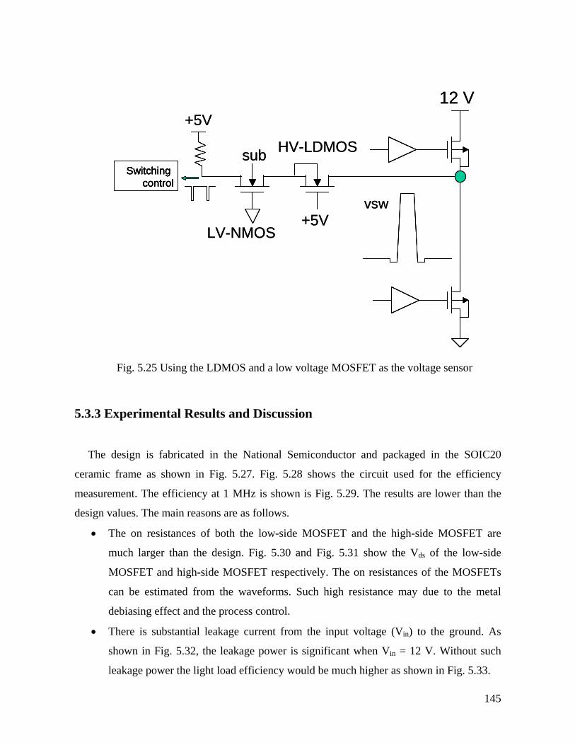
145
+5V
HV-LDMOS
LV-NMOS
Switching control
Switching control
+5V
vsw
12 V
sub
+5V
HV-LDMOS
LV-NMOS
Switching control
Switching control
+5V
vsw
12 V
sub
Fig. 5.25 Using the LDMOS and a low voltage MOSFET as the voltage sensor
5.3.3 Experimental Results and Discussion
The design is fabricated in the National Semiconductor and packaged in the SOIC20
ceramic frame as shown in Fig. 5.27. Fig. 5.28 shows the circuit used for the efficiency
measurement. The efficiency at 1 MHz is shown is Fig. 5.29. The results are lower than the
design values. The main reasons are as follows.
• The on resistances of both the low-side MOSFET and the high-side MOSFET are
much larger than the design. Fig. 5.30 and Fig. 5.31 show the VBdsB of the low-side
MOSFET and high-side MOSFET respectively. The on resistances of the MOSFETs
can be estimated from the waveforms. Such high resistance may due to the metal
debiasing effect and the process control.
• There is substantial leakage current from the input voltage (VBinB) to the ground. As
shown in Fig. 5.32, the leakage power is significant when VBinB = 12 V. Without such
leakage power the light load efficiency would be much higher as shown in Fig. 5.33.

146
Besides the efficiency, the adaptive function of deadtime control also works well. Fig. 5.34
compares the voltage on the switching node with and without adaptive deadtime control. The
durations of the deadtime are reduced significantly when voltage level on the pin ddtime is
high.
6 mm
1.6 mm
6 mm
1.6 mm
Fig. 5.26 Layout of the design
Fig. 5.27 Die in the SOIC20 ceramic frame

147
Vin
5V
L
C1
C2 C3 C4
C5 C6 C7 C8 C9 C10
L and C values use in the test:L=4.5uH C1=100n C2=470u C3,C4=10uC5~C8=22u C9,C10=270u, C11=10u, C12=100n
C12C11
pwm
+5Vcbootgndgnd
gndgnd
ddtime
pbiasvsw
+12Vvsw
+12V
CP
ES
12V
VR
M
vsw
+12Vvsw
gnd
float
Vin
5V
L
C1
C2 C3 C4
C5 C6 C7 C8 C9 C10
L and C values use in the test:L=4.5uH C1=100n C2=470u C3,C4=10uC5~C8=22u C9,C10=270u, C11=10u, C12=100n
C12C11
pwm
+5Vcbootgndgnd
gndgnd
ddtime
pbiasvsw
+12Vvsw
+12V
CP
ES
12V
VR
M
vsw
+12Vvsw
gnd
floatpwm
+5Vcbootgndgnd
gndgnd
ddtime
pbiasvsw
+12Vvsw
+12V
CP
ES
12V
VR
M
vsw
+12Vvsw
gnd
float
Fig. 5.28 Circuit for the efficiency measurement
45
50
55
60
65
70
75
0 1 2 3 4
Output Current (A)
Effi
cien
cy (%
)
Vou t= 1.7VVout = 1.5 VVout = 1.2 VVout = 1.0 V
Fig. 5.29 Measured efficiency Vin=12V @1MHz

148
Vin = 5VVo = 1.75 VIo = 1A
Vdslo = 45 mVRdslo = 45 mΩDesigned value= 21.7 m Ω
Input PWM signal
Output voltage of vsw
Input PWM signal
Output voltage of vsw
Fig. 5.30 Switching waveforms of the low-side MOSFET
Vin = 5VVo = 1.75 VIo = 1A
Vdshi = 180 mVRdshi = 180 mΩDesigned value= 45.4 mΩ
Input PWM signal
Output voltage of vsw
Vin = 5VVo = 1.75 VIo = 1A
Vdshi = 180 mVRdshi = 180 mΩDesigned value= 45.4 mΩ
Input PWM signal
Output voltage of vsw
Input PWM signal
Output voltage of vsw
Fig. 5.31 Switching waveforms of the high-side MOSFET

149
0
100
200
300
400
500
0 2 4 6 8 10 12 14
Vin (V)
Uni
t (m
W)
Leakage powerloss
Fig. 5.32 Leakage power loss
50
55
60
65
70
75
80
85
0 1 2 3 4
Output current (A)
Effi
cien
cy (%
)
With leakage power loss
Without leakage power loss
fs = 1MHz Vout = 1.7 V
Fig. 5.33 Efficiency without the leakage power

150
-1
0
1
2
3
4
5
6
7
0.E+00 1.E-06 2.E-06 3.E-06
Vsw
-1
0
1
2
3
4
5
0.E+00 1.E-06 2.E-06 3.E-06
Vsw
Fixed deadtime
Enable deadtime control
-1
0
1
2
3
4
5
6
7
0.E+00 1.E-06 2.E-06 3.E-06
Vsw
-1
0
1
2
3
4
5
0.E+00 1.E-06 2.E-06 3.E-06
Vsw
Fixed deadtime
Enable deadtime control
Fig. 5.34 Experimental results of the adaptive deadtime control

151
Chapter 6 Optimization of the MOSFET for the Buck Converter
To increase the speed and decrease the power consumption of microprocessors, the on-
board DC-DC converter that powers the microprocessor must operate with high efficiency.
Although much effort has gone toward improving the performance of the converter through
novel topologies and advanced power devices [A25]-[A31], a way to optimize the power
MOSFET based on a specific device technology is not well known [A32]-[A35]. This kind of
an optimization plays an important role in the world of production, because a small change in
the performance and cost can mean the difference between success and failure for a business.
Conventionally, the MOSFET is optimized by a trial-and-error method [B26]. This approach
not only costs money and time, but also never clearly shows whether or not device really
reaches its optimum point.
The effects of various MOSFET design parameters on the efficiency of the buck converter
are studied by FEA in Chapter 4. In this chapter, the conclusions of chapter 4 are employed in
the optimization of the MOSFET for discrete applications. The mixed-mode simulator and the
optimization approach are verified by experimental results.
6.1 PWM-Optimized Power MOSFET
The mathematical definition of optimization is to obtain the best possible design properties
by changing the setting of independent variables in a continuous manner. Usually, there are
two criteria in the optimization: one is the design target to be optimized, and the other
criterion is the constraint on the design. Algebra, calculus and the calculus of variations are
widely used in classic optimization. However, in finite element analysis, optimization is more
difficult, because it takes a significant amount of time to evaluate the effect of the variable on
the design target. This can make the iterative optimization excessively time consuming. The
design variables of the power MOSFET identified and discussed in the Chapter 4 by FEA
simulation are as follows.
• Trench width (WBtB)

152
• Mesa width (WBmB)
• Gate oxide thickness (T Box B)
• The separation between the bottom of the trench and the bottom of the P-body (Ovp).
• Doping concentration of the drift region (N)
• Voltage rating of the power MOSFET (BV)
• Threshold voltage (V BtB)
• Area of the MOSFET (AA)
Because both the high-side MOSFET and the low-side MOSFET have these variables,
there are a total of 16 variables in the optimization. Considering the process simulation, which
may take an hour longer than the mixed-mode circuit simulation, the total simulation time for
evaluating the effect of a single variable is about 1.5 hours. Although the traditional
optimization approach is a possible solution, from the engineering standpoint, a more efficient
way is preferred.
The relationship between the efficiency (E) of the buck converter and the MOSFET design
variables can be expressed as
),...,,,( 321 nXXXXFE = . (6.1)
In the practical variable range, all theses variables can be further classified into two types,
which are described as follows:
[a] 0or0 <∂∂
>∂∂
aa XE
XE (6.2)
The efficiency is a monotonic function of the [a]-type variable. Such variables include the
following.
• Trench width (WBtB) of both the high-side and the low-side MOSFET.
Fig. 4.12 and Fig. 4.24 demonstrate that a narrow trench is preferred for both the low-side
and high-side MOSFETs. The minimum value of WBtB is limited by the photolithography and
etching techniques. For the state-of-art technology, WBtB can be as small as 0.2 um.
• Mesa width (WBmB) of the high-side MOSFET.

153
Fig. 4.14 shows that a wider WBmB is preferred for higher efficiency. However, wider WBmB
also results in much greater silicon area required to achieve less than 0.5% more efficiency.
Therefore, the selection of the mesa width is a tradeoff between cost and performance.
• Mesa width (WBmB) of the low-side MOSFET.
Fig. 4.25 shows that at 300KHz switching frequency, 2.0um WBmB yields the highest
efficiency. However, because the maximum device area is limited by the package and by the
number of devices used as the low-side MOSFET, the maximum device area is less than 25
mmP
2P. Therefore, actually, the smaller WBmB is preferred for both 300KHz and 1MHz switching
frequencies. In addition, the minimum value of Wm is limited by the contact-masking
misalignment tolerance. For the commercial modern MOSFET, WBmB is more than 1 um.
• Gate oxide thickness (T Box B) of both the high-side and the low-side MOSFET.
As shown in Fig. 4.16 and Fig. 4.26, a thinner TBoxB is required for higher efficiency,
although this will lead to larger FOM (Fig. 4.15). The minimum value of TBox B is constrained by
the voltage rating of VBgsB, the typical value of which is about 12 V for the 5V gate-to-source
voltage.
• Doping concentration of the drift region (N) of both the high-side and the low-side
MSOFET
Fig. 4.20 and Fig. 4.28 show that the non-punch-through design is the best in terms of
efficiency. Therefore, the doping concentration of the drift region should be as high as
possible, as long as it can satisfy the breakdown voltage.
[b] 0=∂∂
= bib XXbXE (6.3)
This type of parameter plays an important role in the efficiency and should therefore be
optimized, because the maximum E occurs at
0...321
=∂
==∂
=∂
=∂
bNbbb XE
XE
XE
XE . (6.4)
The following design parameters can be identified as [b]-type variables.

154
• Ovp of both low-side and high-side MOSFET
As shown in Fig. 4.18 and Fig. 4.27, the optimum value of Ovp is about zero. And this
value is valid for both the high-side and the low-side MOSFETs at different switching
frequencies.
• Voltage rating (BV) of both the low-side and high-side MOSFET
Fig. 4.21 and Fig. 4.29 show that the 30V BV is a good candidate for use in the 20V-input
DC-DC converter.
• Threshold voltage of both the low-side and high-side MOSFETs
As shown in Fig. 4.23 and Fig. 4.30, the low-side and high-side MOSFETs have different
optimized threshold voltages. The minimum value of the threshold voltage is limited by the
noise immunity requirement of the circuit.
• Device area of both the low-side and high-side MOSFETs
Actually, device area is the most important design parameter of the MOSFET, because it is
directly related to the cost of the device. As shown in the simulation results presented in
Chapter 4, there is always an optimized area for both the low-side and the high-side
MOSFETs. Assuming Aop is the optimized area, if the designed device area is larger than
Aop, this design is a failure, because the extra device area (A - Aop) decreases efficiency; if
the designed device area is less than Aop, there is generally a tradeoff between the efficiency
and the device area.

155
Table 6.1 A summary of the PWM-optimized MSOFET.
Design parameter Design trend Comment
Hi-MOS Narrower Trench width
(WBtB) Lo-MOS Narrower
Limited by litho and
etching techniques
Hi-MOS Wider Tradeoff btw cost and E Mesa width
(WBmB) Lo-MOS Narrower Limited by misalignment
Hi-MOS Thinner Gate oxide
thickness (Tox) Lo-MOS Thinner
Limited by the voltage
rating of Vgs
Hi-MOS Non-punch-through Doping
concentration of the
drift region (N)
Lo-MOS Non-punch-through
Limited by the breakdown
voltage
Hi-MOS Optimized Spr btw trench btm
& P-body btm (Ovp) Lo-MOS Optimized
Optimized value is close to
zero
Hi-MOS Optimized Breakdown voltage
(BV) Lo-MOS Optimized
For 20V input, 30 V is
close to optimized value.
Hi-MOS Optimized Threshold voltage
(VBtB) Lo-MOS Optimized
Lowest VBtB is limited by the
noise immunity capability.
Hi-MOS Optimized Device area
(AA) Lo-MOS Optimized
Most important design
parameters
Traditionally, the PWM-optimized MOSFET means that the FOM is reduced by fine-
tuning the design variable of WBtB, WBmB, Ovp and TBoxB. However, there are two disagreements
between the design trends for the minimized FOM and maximized efficiency.
• Gate oxide thickness.
Fig. 4.15 shows that thick gate oxide is needed to achieve less FOM. However, Fig. 4.16
and Fig. 4.26 show that the thinner gate oxide is preferred for higher efficiency.
• The mesa width of the low-side MOSFET
Fig. 4.15 shows that wider mesa is needed to achieve less FOM. However, because the
maximum device area is limited by the package type and the number of MOSFETs used in the

156
circuit, a narrower mesa is better. In fact, the efficiency is not sensitive when the mesa width
ranges from 1.0 um to 1.5 um.
Table 6.1 lists the design trends for various parameters of both the high-side and low-side
MOSFETs for 20V input voltage and 300KHz switching frequency. If we assume that the
optimized parameters of the MOSFET structure are independent of the other design variables,
then the PWM-optimized MOSFETs have the following features.
• Narrower trench.
• Thinner gate oxide.
• Non-punch-through design of the drift region.
• Zero separation between the bottom of the trench and the bottom of the P-body.
• Narrower mesa of the low-side MOSFET.
• Wider mesa of the high-side MOSFET.
6.2 Optimization Based on PWM Optimized Power MOSFET
Two optimization procedures are described in this section. The first one uses the traditional
Hooke-Jeeves algorithm; the second uses a decoupling method to decrease the simulation
time.
6.2.1 Optimization Using Hooke-Jeeves Algorithm
The Hooke-Jeeves algorithm is a traditional optimization method for multi-variable
problems. Basically, this approach starts from the initial condition and searches for the correct
direction of each variable’s variation. If the direction is good, it will increase the variation
step. Otherwise, it searches for the direction again until it meets the criteria.
Fig. 6.1 shows the optimization procedure of the MOSFET. There are four function blocks
in Fig. 6.1 as follows.

157
• The Mixed Mode Circuit Simulator is the circuit simulator, which uses an FEA model
for the two power MOSFETs and a Pspice model for the driver. The FEA models are
generated by the block of the Device Simulator. The device areas are given by the
block of Performance Evaluation and Procedure Control.
• The Device Simulator performs the device simulation, providing basic electrical
characteristics of the MOSFET.
• The Process Simulator inputs parameters that are controlled by the Performance
Evaluation and Procedure Control block.
• The Performance Evaluation and Procedure Control calculates the efficiency of the
circuit and determines how to try the next variable value. It feeds the MOSFET design
parameters to the Process Simulator block and the device area data to the Mixed-Mode
Circuit Simulator block
As an example, the optimization can be performed using the device area (ABhiB) and P-body
doping (PBbdhiB) of the high-side MOSFET, and the device are (ABloB) and P-body doping (PBbdloB) of
the low-side MOSFET. The final result obtained by using the Hooke-Jeeves algorithm is
shown in Fig. 6.2, where the starting conditions are V BthiB=1.24 V, ABhiB=2.4mmP
2P, VBtloB=1.86 V,
ABloB=4.8mmP
2P, and E=83.51% and the optimized results are VBthiB=1.51V, ABhiB=1.2mmP
2P, VBtloB=2.12
V, ABloB=7.44mmP
2P, and E=85.89%. The optimization process results in an optimized device
area with higher efficiency.
6.2.2 Optimization Using Decoupled Loops
The preceding optimization process can be realized, but it takes a long time to run the
whole simulation cycle. Assume the time needed for the mixed-mode circuit simulation is TB0B,
and the process simulation takes KT B0 B (usually process simulation takes much longer than the
circuit simulation, and K>>1): if only the device area is changed, it will take TB0B to reach a
new value of the target function. However, if the P-body dose is changed, it will take (K+1)TB0B
to run the process simulation. For the example shown in Fig. 6.2, half of the simulation steps
are the process simulation. The total simulation time is about 31(K+1)TB0 B (for P-body
change)+31TB0 B (for area change), and most of time (31KTB0 B) is spent on the process simulation.

158
Therefore, we need to find another algorithm that spends less time on the process simulation.
Because the loss of the high-side MOSFET (P BhiB) consists of turn-on loss, turn-off loss and
conduction loss, the parameters A BloB and VBtloB do not greatly affect the PBhiB. Therefore, ABhiB and
VBtloB can be optimized first, and then ABloB and VBtloB can be optimized. As proposed in Fig. 6.3,
because the optimization of the threshold voltage is placed at the outer loop, the number of the
process simulation is minimized in order to save computation time. One optimization example
is shown in Fig. 6.4, and the optimized results are VBthiB=1.40V, ABhiB=0.95mmP
2P, VBtloB=1.97 V,
ABloB=6.18mmP
2P, and E=85.87%. Compared to the results found by the Hooke-Jeeves method,
the efficiency is almost the same. Although it takes more steps for the optimization, the total
computation time is actually reduced by 30%, because most of the steps are spent on the
circuit simulation.
6.3 A Design Example and Experimental Results
So far, all the discussion and conclusions are based on the simulation results. In this
section, a design example is presented to answer two fundamental questions.
• How accurate is the FEA model?
• Is the design guideline of the PWM-optimized MOSFET described in sedction 6.1
correct?
The first question can be answered by a comparison between the simulation and
experimental results. The second question is answered by comparing the efficiency with the
most recently released product from one of the major suppliers (R company) of low-voltage
MOSFET for the notebook application.
6.3.1 Design Background
Since the efficiency of the buck converter depends not only on the performance of the
power MOSFET but also on other factors, the design environment should be defined and
justified before the optimization of the power MOSFET.

159
• Selection of driver
The driver of the power MOSFET plays an important role in the optimization of the
MOSFET, because the switching loss of the high-side MOSFET and the deadtime power loss
of the low-side MOSFET are directly related to the characteristics of the driver. Currently,
there are two major suppliers of the driver for the notebook application. They are MAXIM
and INTERSIL. This design uses MAX1718 as the driver/controller, and the efficiency tests
are performed on the commercial efficiency evaluation board MAX1718MS.
• Switching frequency
MAX1718 supports four switching frequencies: 200, 300, 550 and 1,000 KHZ. The 300
KHz is selected as the design parameter, because it is still widely used in the industry. The
efficiency at higher switching frequencies is also tested, and will be presented in this chapter.
• Input voltage
The input voltage has a substantial impact on the switching loss of the high-side MOSFET.
In the notebook application, the highest input voltage is 20 V. This is the worst case in terms
of the switching loss; therefore, 20 V is selected as the design parameter.
• Output voltage
The output voltage of MAX1718 ranges from 0.6 V to 1.75 V. 1.3 V is selected as the
design parameter.
• Load current
Load current affects not only the switching loss of the high-side MOSFET, but also the
conduction loss of both MOSFETs. The 20 A for each phase is usually used to compare
efficiency.
For a long time, R company's products have dominate the market of the high-side
MOSFET for the notebook application, while the most popular low-side MOSFETs are

160
provided by the S company. This design focuses on the optimization of the high-side
MOSFET using S company's device (SL) as the low-side MOSFET.
Package, driver andboard parameters
Optimized MOSFET processand device area
Process Simulator
Device Simulator
Mixed ModeCircuit Simulator
Performance Evaluationand Procedure Control
Loop2
Loop1
Finite Element Analysis (FEA)
Initial MOSFET processand device area
Package, driver andboard parameters
Optimized MOSFET processand device area
Process Simulator
Device Simulator
Mixed ModeCircuit Simulator
Performance Evaluationand Procedure Control
Loop2
Loop1
Finite Element Analysis (FEA)
Initial MOSFET processand device area
Fig. 6.1 General optimization procedure
83
83.5
84
84.5
85
85.5
86
86.5
0 20 40 60steps
Effi
cien
cy (%
)
Hooke-Jeeves algorithm
Fig. 6.2 An optimization example using Hooke-Jeeves algorithm
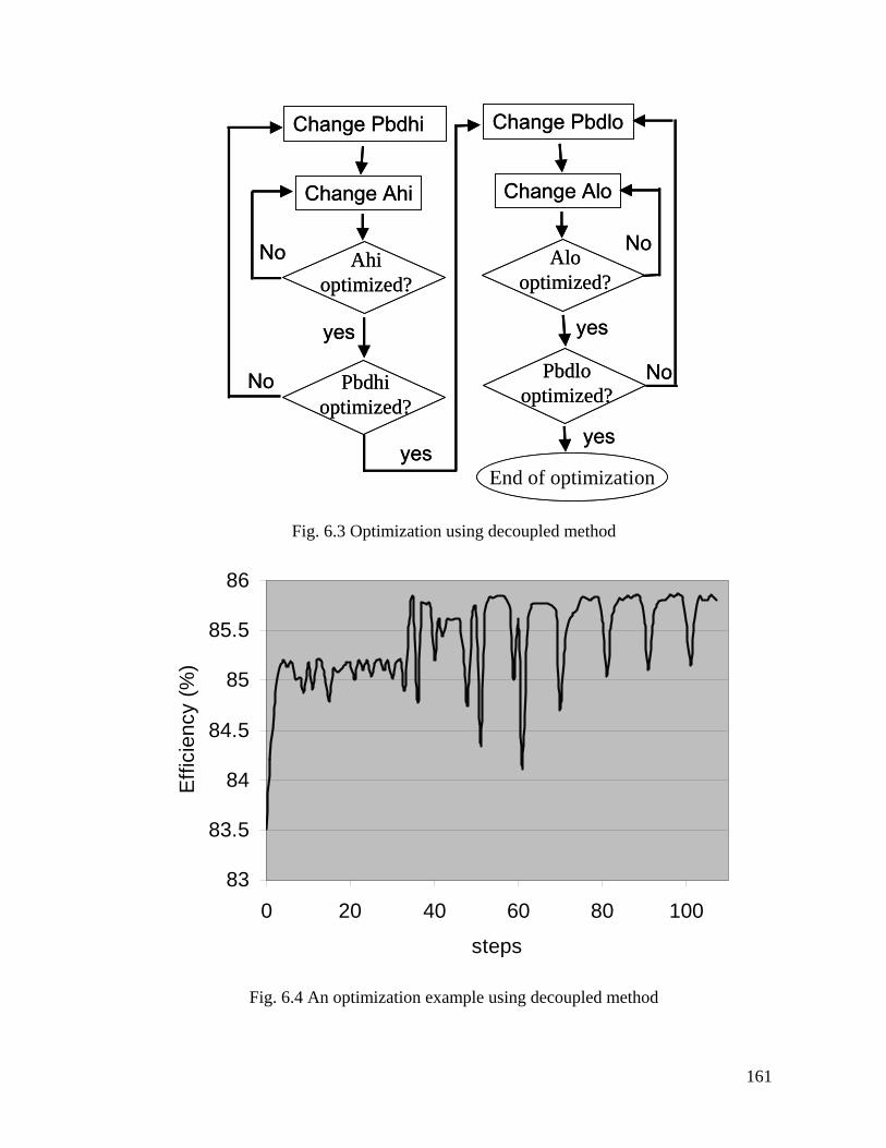
161
Change Pbdhi
Change Ahi
Ahioptimized?
No
yes
Pbdhioptimized?
No
Change Pbdlo
Change Alo
Alooptimized?
No
yes
Pbdlooptimized?
No
yesEnd of optimization
yes
Change Pbdhi
Change Ahi
Ahioptimized?
No
yes
Pbdhioptimized?
No
Change Pbdlo
Change Alo
Alooptimized?
No
yes
Pbdlooptimized?
No
yesEnd of optimization
yes
Fig. 6.3 Optimization using decoupled method
83
83.5
84
84.5
85
85.5
86
0 20 40 60 80 100
steps
Effic
ienc
y (%
)
Fig. 6.4 An optimization example using decoupled method

162
6.3.2 Design Procedure
Some optimization approaches are presented in section 6.2. Actually, the design procedure
can be rather flexible as based on PWM-optimized MOSFET, because a tradeoff between the
device area and the performance exists in the design of the high-side MOSFET. As addressed
in section 6.2, the wider mesa is preferred for higher efficiency. However, in order to achieve
1% higher efficiency, the area of the MOSFET may double. Therefore, instead of using the
maximum device area for the highest efficiency, the device areas are optimized based on two
different mesa widths, which are selected for the purposes of cost reduction with a narrower
mesa (high-density), and higher efficiency with a wider mesa (low-density).
The simulated efficiency is shown in Fig. 6.5. In the efficiency calculation, a fixed
magnetic loss is used for the filter inductor. Although this value can substantially affect the
absolute efficiency value, it has trivial influence on the optimization of the MOSFET. On the
other hand, the magnetic loss is also almost independent of the power MOSFET, because its
loss is determined by both the current and the switching frequency.
In Fig. 6.5, the H design is selected for the purpose of low cost. If the device area is less
than H, there is a dramatic drop in efficiency. However, the L design is selected for the
purpose of high efficiency.
6.3.3 Experimental Results and Discussion
In order to minimize the error of the efficiency test, the measurement is controlled by the
computer. For each test point, a duration of five minutes is used for the burn-in time to make
sure the circuit and the operation temperature reach the steady state. Then, the input voltage,
input current, output voltage and output current are sampled every 30 seconds. After
eliminating the three minimum and three maximum values of the data, the efficiency is
calculated using the average value by
inin
outout
IVIV
××
=η . (6.5)

163
The experiment shows that the error of the efficiency is within 1%. The gate loss is not
included in the optimization and the test, because of the following.
• The gate loss is much less than the conduction and switching losses at 300 KHz.
• It is unlikely that the gate loss can be accurately measured, because it is not easy to
separate the gate loss from the driver loss.
• Currently, for the notebook application, industry does not consider the gate loss in the
efficiency measurement.
Fig. 6.6 compares the simulated and measured efficiencies of the H and L designs at
switching frequencies of 300 KHz and 500 KHz. Good agreements are achieved at both
frequencies.
Fig. 6.7 summarizes the efficiency and the device area at the two switching frequencies.
The design target is achieved at 300 KHz by the L design in terms of the performance.
Compared to R, H is still a better design, because its area is less than one-third of R, while the
efficiency is only lower by 0.1%. At 500 KHz, designs H and L beat R in terms of both cost
and performance.
The experimental results demonstrate that the design based on the PWM-optimized
MOSFET, using the mixed-mode simulation is successful.

164
83.5
84
84.5
85
85.5
86
0 1 2 3 4 5 6 7 8
Normalized device area
Effi
cien
cy (%
)
High density designLow density designDesign HDesign L
Fig. 6.5 Simulated efficiency of the design.
79
80
81
82
83
84
85
86
87
Simula
ted H
@30
0K
Measu
red H
@30
0K
Simula
ted H
@55
0K
Measu
red H
@55
0K
Simula
ted L@
300K
Measu
red L@
300K
Simula
ted L@
550K
Measu
red L@
550K
Effic
ienc
y (%
)
Fig. 6.6 Comparison of the measured and simulated efficiency at full load.

80
81
82
83
84
85
86
0 1 2 3 4 5Normalized device area
Effi
cien
cy (%
)
Efficiency @300K Iout=40A
Efficiency @500K Iout=40A
H design
L designR design
80
81
82
83
84
85
86
0 1 2 3 4 5Normalized device area
Effi
cien
cy (%
)
Efficiency @300K Iout=40A
Efficiency @500K Iout=40A
H design
L designR design
Fig. 6.7 Comparison of the efficiency and device area.
165

Chapter 7 Conclusions and Future Work
7.1 Conclusions
In the high-frequency DC-DC buck converter, which is the required voltage supply of
microprocessors, the performance of the power MOSFETs (including the high-side MOSFET
and the low-side MOSFET) can not be accurately predicted by traditional analytical models,
because the parasitic elements of the package and the PCB and nonlinear characteristics of the
power MOSFETs play a more important role in the switching process. The complexities of
both the turn-on and the turn-off processes of the high-side MOSFET and the possible
spurious turn-on loss of the low-side MOSFET are demonstrated in this dissertation. In order
to achieve good MOSFET design, the FEA model must be employed in the evaluation of
various losses associated with the power MOSFETs.
Although FEA has long been widely used in semiconductor modeling, it has not been
employed in the buck converter due to the convergence problem and the long simulation time
needed for the circuit to reach the steady state. In this dissertation, the convergence problem is
solved by setting the initial voltage and current of the buck circuit to zero and then ramping
the voltage and current up to the desired values; the simulation time is reduced by using the
current source instead of LCR network as the load; hence, the circuit can avoid the transient
process and can immediately enter the stead state. With the help of the power loss extraction
program, both the detailed power loss information for the MOSFET and the parasitic elements
can be determined quickly and conveniently. This FEA method not only takes into account
the nonlinear effect of the MOSFET, the driving capability of the controller/driver, and the
major parasitic components of the circuit, but also directly links the power loss of the
MOSFETs to the device structure and the device technology.
The design trends of PWM-optimized MOSFETs are studied by extensive simulation. The
major tradeoff between cost and performance is identified. Finally, a successful design is
166

167
demonstrated. Compared with the mainstream commercial MOSFET, the design not only has
small device area (low cost), but also has higher efficiency at its designed operation condition.
Therefore, the proposed FEA method provides a novel methodology for the PWM-optimized
MOSFETs.
7.2 Summary of Research Contributions
This dissertation is dedicated to the optimization of the low-voltage MOSFET used in the
high-frequency buck converter. Besides the high precision FEA model, several other novel
models are developed to achieve greater understanding if the dynamic process of both the
high-side and the low-side MOSFETs. In addition, the feasibility of monolithic integration of
the buck converter is investigated in terms of the process and device optimization.
The major research contributions associated with this dissertation are listed below.
• A novel model for MOSFET switching loss calculation. This model describes the
effect of the parasitic inductance on the switching process.
• A novel model for the dt/dv induced spurious turn-on voltage. This model takes into
account the parasitic inductance in the analytical solution.
• A novel model for QBgd B calculation. This model describes the influences of the gate
oxide and the doping condition of the drift region on the QBgd B. Ignoring the parasitic
inductance, the turn-on and turn-off loss processes of the power MOSFET can be
predicted by this model.
• The FEA model is applied to the simulation of the buck converter. By solving the
convergence problem and dramatically reducing the simulation time, the switching
performance of the power MOSFET in the buck converter is extensively studied. The
design trench of the PWM-optimized power MOSFETs are identified.
• Based on the FEA simulation, different optimization approaches of the MOSFETs are
studied and verified experimentally by a successful MOSFET design for the notebook
application.

168
• An economical 5V/20V CMOS-compatible power IC process is proposed. The
isolation capability and the device performance are demonstrated experimentally.
• A novel adaptive deadtime control method for the monolithic integrated buck
converter can detect the two deadtimes in one switching cycle, and is absolutely
compatible with the power IC process.
7.3 Future Research Directions
In this dissertation, the application of the FEA model focuses on the optimization of the
traditional power UMOSFET used in the synchronous buck converter for the personal
computer. However, this technique can be extended to other research areas as the follows.
(1) System optimization.
The optimization of the MOSFET strongly depends on its operation conditions. Although
for a MOSFET designer, the operation conditions are fixed, from the system standpoint, these
variables are subject to change. Examples of these variables include the input voltage of the
buck converter, the gate driving voltage of the MOSFET, etc. Now, these parameters can be
determined more accurately.
(2) Evaluation of new circuit topologies.
Besides the traditional synchronous buck converter, there are other topologies [D17]-[D19]
for the high-frequency DC-DC application. After proper modification of the circuit, the FEA
model also can be used to calculate its power loss and to help select the MOSFET. In
addition, the advantage of the new idea can be verified more academically.
(3) Evaluation of new device structures.
Although the UMOSFET is the most popular power device adopted by the high-frequency
DC-DC converter, other device structures [A6],[A7], [A36]-[A40] are also potential
candidates. Because the FEA model is directly based the physical structure of the device, this
method can be conveniently used to investigate the switching performance of other devices.

Therefore, not only the device designer, but also the circuit and system engineers, can
benefit from the new simulation method proposed in this dissertation. I hope my approach can
contribute to these areas in the near future.
169

170
REFERENCES
A. Physics and Characteristics of Power Device
[A1] Syotaro Ono, Yusuke Kawaguchi and Akio Nakagawa, "30V new fine trench
MOSFET with ultra low on-resistance," IEEE ISPSD'03, pp. 28-31.
[A2] Jun Zeng, et al., "An ultra dense trench-gated power MOSFET technology using a
self-aligned process," IEEE ISPSD'01, pp. 147-150.
[A3] Steven T. Peake, et al., "Fully self-aligned power trench-MOSFET utilizing 1um pitch
and 0.2um trench width," IEEE ISPSD'02, pp. 29-32.
[A4] A. Narazaki, et al., “A 0.35 um trench gate MOSFET with an ultra low on state
resistance and a high destruction immunity during the inductive switching,” IEEE ISPSD’00,
pp. 377-380.
[A5] M. A. A. in ‘t Zandt, et al., “Record-low 4 mΩ.mmP
2P specific on-resistance for 20V
trench MOSFETs,” IEEE ISPSD’03, pp.32-35.
[A6] Akihiko Osawa, et al., "2.5 V-driven Nch 3rd generation trench gate MOSFET," IEEE
ISPSD'99, pp. 209-212.
[A7] Hitoshi Yamaguchi, et al., "Ultra low on-resistance super 3D MOSFET," IEEE
ISPSD'03, pp. 316-319.
[A8] International Rectifier MOSFET IRF7832 datasheet.
[A9] Siliconix MOSFET Si4362DY datasheet.
[A10] Siliconix MOSFET Si4364DY datasheet.
[A11] International Rectifier MOSFET IRF7821 datasheet.
[A12] International Rectifier MOSFET IRF7811A datasheet.
[A13] Alpha&Omega MOSFET AO4406 datasheet.
[A14] Siliconix MOSFET Si4892DY datasheet.
[A15] Siliconix MOSFET Si4860DY datasheet.
[A16] A. Q. Huang, N. X. Sun, B. Zhang, X. Zhou and F. C. Lee, "Low voltage power
devices for future VRM," IEEE ISPSD'98, pp. 395-398.
[A17] V. Parthasarathy, et al., “A 33V, 0.25mΩ-cm2 n-channel LDMOS in a 0.65um smart
power technology for 20-30 V applications,” IEEE ISPSD’98, pp. 61-64.

171
[A18] Tsutomu Uesugi, et al., “New 3-D lateral power MOSFETs with ultra low on-
resistance,” IEEE ISPSD’98, pp. 57-60.
[A19] Steve Merchant, et al., “High performance 20-30 V LDMOS transistors in a 0.65 um-
based BiCMOS compatible process,” IEEE BCTM’97, pp. 202-205.
[A20] A Sugi, et al., “A 30V class extremely low on-resistance meshed trench lateral power
MOSFET,” IEEE ISPSD’02, pp. 297-300.
[A21] Shuming Xu, et al., “Folded gate LDMOS with low on-resistance and high
transconductance,” IEEE ISPSD’00, pp. 55-58.
[A22] Akio Nakagawa and Yusuke Kawaguchi, “Improved 20V lateral trench gate power
MOSFETs with very low on-resistance of 7.8 mΩ.mmP
2P,” IEEE ISPSD’00, pp. 47-50.
[A23] N. Fujishima, et al., “A high density, low on-resistance, trench lateral power MOSFET
with a trench bottom source contact,” IEEE ISPSD’01, pp. 143-146.
[A24] Nick X. Sun, Alex Q. Huang, et al., "An 0.35-um, 6-mΩ, 43 uΩ-cm2 lateral power
MOSFET for low-voltage Megaherz switching power applications," IEEE Electron Device
Letters, Vol. 20, No. 7, July 1999, pp. 351-353.
[A25] Mohamed Darwish, et al., "A new power W-gated trench MOSFET(WMOSFET) with
high switching performance," IEEE ISPSD'03, pp. 24-27.
[A26] Jun Zeng and C. Frank Wheatley, “An improved power MOSFET using a novel split
well structure,” IEEE ISPSD’99, pp. 205-208.
[A27] D. Ueda, H. Takagi and G. Kano, "A new vertical power MOSFET structure with
extremely reduced on-resistance," IEEE Transactions on Electron Devices, ED-32, 1985, pp.
2-6.
[A28] Jack Glenn and Jim Siekkinen, “A novel vertical deep trench RESURF DMOS,” IEEE
ISPSD’00, pp. 197-200.
[A29] Ping Li, et al., "Novel power MOS devices with SiGe/Si heterojunctions," IEEE
ISPSD'00, pp. 109-112.
[A30] Timothy Henson and Joe Cao, "Low voltage super junction MOSFET simulation and
experiment," IEEE ISPSD'03, pp. 37-40.
[A31] D. Ueda, H. Takagi and G. Kano, “A new vertical double diffused MOSFET- the self-
aligned terraced-gate MOSFET,” IEEE Trans. Electron Devices, ED-31, 1984, pp. 416-420.

[A32] C. S. Mitter, "Device consideration for high current, low voltage synchronous buck
regulator (SBR)," IEEE Conference: Wescon'97, Santa Clara, CA, pp. 281-288.
[A33] C. Hu, M. H. Chi and V. M. Patel, “Optimum design of MOSFETs,” IEEE Trans.
Electron Devices,” ED-31, 1984, pp.1963-1700.
[A34] J. Lambert and D. Jauregui, "Optimized MOSFETs improve 1MHz multi-phase
converters," PCIM Magazine, May 2000.
[A35] S. Deuty, "Optimizing transistor performance in synchronous rectifier, buck
converters," PCIM Magazine, May 2000.
[A36] R. Sodhi, R. Malik, D. Asselanis and D. Kinzer, "High-density ultra-low Rdson 30
volt N-channel trench FETs for DC/DC converter applications," IEEE ISPSD'99, pp. 307-310.
[A37] Ling Ma, et al., "New trench MOSFET technology for DC-DC converter
Applications," ISPSD'03, pp. 354-357.
[A38] Jongdae Kim, et al., “High-density low on-resistance trench MOSFETs employing
oxide spacers and self-align technique for DC/DC converter,” IEEE ISPSD’00, pp. 381-384.
[A39] Sameh G. Nassif-Khalil, Shahla Honarkhah and C. Andre T. Salama, “Low voltage
CMOS compatible power MOSFET for on-chip DC/DC converters,” IEEE ISPSD’00, pp. 43-
46.
[A40] Norio Yasuhara, et al., "Low gate charge 30 V N-channel LDMOS for DC-DC
converters," IEEE ISPSD'03, pp. 186-189.
B. Modeling of Power Devices
[B1] K. G. P. Dharmawardana and G. A. J. Amaratunga, "Analytical model for high current
density trench gate MOSFET," IEEE ISPSD'98, pp. 351-354.
[B2] M. G. L. van den Heuvel, et al., "An improved method for determining the inversion
layer mobility of electrons in trench MOSFETs," IEEE ISPSD'03, pp. 173-176.
[B3] Mohamed Darwish, “Study of the quasi-saturation effect in VDMOS transistors,”
IEEE Transactions on Electron Devices, Vol. ED-33, No. 11, Nov. 1986, pp. 1710-1716.
[B4] K. H. Lou, C. M. Liu and J. B. Kuo, “Analysis of the quasi-saturation behavior
considering the drain-to-source voltage and cell-spacing effects for a vertical DMOS power
transistor,” Solid State Electronics, Vol. 36, No. 1, 1993, pp. 85-91.
172

[B5] C. L. Ma and P. O. Lauritzen, "Modeling of power diodes with the lumped-charge
modeling technique," IEEE Trans. on Power Electronics, Vol. 12, 1997, pp. 198-405.
[B6] Ph. Leturcq, et al., “Full dynamic power bipolar device models for circuit simulation,”
IEEE PESC’98, pp. 1695-1703.
[B7] Ph. Leturcq, et al. "Implementation and validation of a new diode model for circuit
simulation," IEEE PESC'96, pp. 35-43.
[B8] Yuming Bai and Alex Q. Huang, “A novel power diode hybrid model for circuit
simulation,” IEEE COMPEL, July 2000.
[B9] H. Morel, et al., “State variable modeling of the power PIN diode using an explicit
approximation of semiconductor Equations: a novel approach,” IEEE Trans. on Power
Electronics, Vol. 9, 1994, pp. 112-120.
[B10] A. G. M. Strollo, “A new SPICE model of power PIN diode based on asymptotic
waveform evaluation,” IEEE Trans. on Power Electronics, Vol. 12, 1997, pp. 12-20.
[B11] H. Goebel, “A unified method for modeling semiconductor power devices,” IEEE
Trans. on Power Electronics, Vol. 9, 1994, pp. 497-505.
[B12] M. Trievdi, et al., “Performance modeling of power MOSFETs,: IEEE Trans. Electron
Devices, ED-46, 1999, pp. 1794-1802.
[B13] Duncan A. Grant and John Gowar, "Power MOSFETs: Theory and Applications,"
New York: John Wiley & Sons, 1989.
[B14] S. Shinohara, "Analysis of power losses in MOFET synchronous rectifiers by using
their design parameters," IEEE ISPSD'98, pp. 347-350.
[B15] Larry Spaziani, "A study of MOSFET performance in processor targeted buck and
synchronous rectifier buck converters," HPFC'96, pp.123-137.
[B16] Yuming Bai, Yu Meng, Alex Q. Huang, Fred C. Lee, "A novel model for MOSFET
switching loss calculation," IEEE IEPMC, 2003.
[B17] Yuming Bai, Yu Meng, Alex Q. Huang and Fred C. Lee, "Study of power loss in DC-
DC converter using finite element analysis," IEEE IEPMC, 2003.
[B18] R. J. E. Hueting, et al., "Switching performance of low-voltage N-channel trench
MOSFETs," IEEE ISPSD’02, pp. 177-180.
[B19] S. M. Clementi, B. R. Pelly and A. Isidori, "Understanding power MOSFET switching
performance," IEEE IAS'81, pp. 763-776.
173

[B20] T. Sloane, H. Owen and T. Wilson, "Switching transients in high frequency, high
power converter using power MOSFET's," International Rectifier Application Note AN933.
[B21] Thomas Wu, "Cdt/dt induced turn-on in synchronous buck regulators," Technical
paper of International Rectifier.
[B22] R. Severns, "dV/dt effects in MOSFET and bipolar junction transistor switches," IEEE
PESC, June 1981, pp. 258-264.
[B23] Yuming Bai, Deva Pattanayak and Alex Q. Huang, "Analysis of dv/dt induced
spurious turn-on of MOSFET," CPES Annual Seminar, 2003.
[B24] Yuming Bai and Alex Q. Huang, “Novel automated optimization of power MOSFET
for 12V input, high-frequency DC-DC converter,” IEEE ISPSD'03, pp.366-369.
[B25] B. J. Baliga, "Power semiconductor device figure of merit for high frequency
applications," IEEE Electron Device Letter, Vol. EDL-10, pp. 455-457, 1989.
[B26] Ritu Sodhi, Steve Brown Sr. and Dan Kinzer, "Integrated design environment for
DC/DC converter FET optimization," IEEE ISPSD'99, pp. 241-244, 1999.
[B27] R. K. Kraus and H. J. Mattausch, "Status and trends of power semiconductor models
for circuit simulation,", IEEE Tans. On Power Electronics, Vol. 13, pp. 452-465, 1998.
[B28] Philippe Leturcq, "Power Semiconductor Device Modeling Dedicated to Circuit
Simulation," IEEE ISPSD'99, pp. 19-26, 1999.
[B29] R. Kraus et al,. "Physics-based models of power semiconductor devices for the circuit
simulator SPICE", IEEE PESC'98, pp. 1726-1731.
[B30] H. Goebel, "A unified method for modeling semiconductor power devices," IEEE
Trans. on Power Electronics, vol. 9, pp. 497-505, 1994.
C. Technology of Device and Package
[C1]Jongdae, et al., "A novel process technique for fabricating high reliable trench MOSFETs
using self-align technique and hydrogen annealing," IEEE ISPSD'01, pp. 139-142.
[C2] Sang-Gi Kim, et al., “Trench corner rounding technology using hydrogen annealing for
highly reliable trench MOSFETs,” IEEE ISPSD’00, pp. 87-90.
[C3] Naresh Thapar, et al., “MOSFET technology advances DC-DC converter efficiency
for processor power,” IEEE PCIM 2001.
174

[C4] Jongdae, et al., “High-density trench DMOSFETs employing two step trench
technique and trench contact structure,” IEEE ISPSD’03, pp. 165-168.
[C5] K. Shenai, “Optimized trench MOSFET technologies for power devices”, IEEE Trans,
Electron Devices, 39(6), p1435,1992.
[C6] Il-Yong Park, et al., "Novel process techniques for fabricating high density trench
MOSFETs with self-aligned N+/P+ source formed on the trench side wall," IEEE ISPSD'03,
pp. 169-172.
[C 7] D. Grant, et al., "A 3V to 6V out synchronous buck PEM integrated FET switcher
design uses state-of-art power IC technology," IEEE ISPSD'02, pp. 213-216.
[C8] C. Bulucea and R. Rossen, "Trench DMOS transistor technology for high-current
(100A range) switching," Solid-State Electronics, 1991, pp. 493-507.
[C9] S. Matsumoto, T. Ohno and K. Izumi, "Ultralow specific on resistance UMOSFET
with trench contacts for source and body regions realized by self aligned process," Electronic
Letters, August 1991, pp. 1640-1642.
[C10] Richard K. Williams, “Beyond Y2K: Technology convergence as a driver of future
low-voltage power management semiconductors,” IEEE ISPSD’00, pp. 19-22.
[C11] V. Parthasarathy, et al., “A 0.35 um CMOS based smart power technology for 7V-50V
applications,” IEEE ISPSD’00, pp. 317-320.
[C12] N. X. Sun, A. Huang and F. C. Lee, "Design of a 4 MHz, 5V to 1V monolithic voltage
regulator chip," IEEE ISPSD'02, pp. 221-224.
[C13] F. De Pestel, et al., "Development of a robust 50V 0.35um based smart power
technology using trench isolation," IEEE ISPSD'03, pp. 182-185.
[C14] A. Moscatelli, et al., "LDMOS implementation in a 0.35 um BCD technology
(BCD6)," IEEE ISPSD'00, pp. 323-326.
[C15] Mohamed Darvish, et al., "Scaling issues in lateral power MOSFETs," IEEE
ISPSD'98, pp. 329-332.
[C16] Alex Q. Huang, et al., “Monolithic integration of 5-V CMOS and high-voltage
devices,” IEEE Electron Device Letters, Vol. 13, 1992, pp. 575-577.
[C17] Mark Pavier, et al., "Understanding the effect of power MOSFET package parasitics
on VRM circuit efficiency at frequencies abover 1MHz," PCIM 2003.
175

[C18] Carl Blake, Ralph Monteiro and Andrew Sawle, "High current voltage regulator
module employs novel packaging technology to achieve over 100A in a compact footprint to
power next generation servers," PCIM 2002.
[C19] Ralph Monteiro, Carl Blake and Jason Chiu, "Direct FETTM power MOSFET
packaging technology enables discrete multiphase converter design capable of up to
2MHz/phase operation," PCIM 2003.
[C20] A. Tsui, M. Kasem, W. McDaniel and El. Lambka, "Direct interconnect: New
MOSFET package cuts on-resistance," PCIM Magazine, Aug. 1999, pp. 20-30.
[C21] Simon S. Wen, Daniel Huff and Guo-Quan Lu, "Dimple-array interconnet technique
for packaging power semiconductor devices and modules," IEEE ISPSD'01, pp. 69-74.
[C22] Aram Arzumanyan, et al., "Flip chip power MOSFET: A new wafer scale packaging
technique," IEEE ISPSD'01, pp. 251-254.
[C23] Y. Xiao, et al., "Flip-chip flex-circuit packaging for power electronics," IEEE
ISPSD'01, pp. 55-58.
[C24] Terry Ericsen, "New power switch packaging technologies," PCIM, May 1999, pp.
28-30.
[C25] Fisher R., et al., "High frequency, low cost, power packaging using thin film power
overlay technology," IEEE APEC'95, pp. 12-17.
[C26] Jon Klein, "Bottomless So-8 package boosts MOSFET performance," PCIM, 2000,
pp. 100.
[C27] Patrick Mannion, "MOSFETs break out of the shackles of wirebonding," Electronic
Design, March 1999, pp. 36.
D. VRM Technologies
[D1] J. G. Renauer, "Challenges in powering high performance, low voltage processors,"
IEEE APEC, 1996.
[D2] S. Goodfellow and D. Weiss, "Designing power systems around processor
specifications," Electronic Design, Jan. 1997.
[D3] Frank Goodenough, "Advanced microprocessors demand amperes of current at < 2V,"
Electronic Design, Jan. 20, 1997.
176

[D4] M. Zhang, M. Jovanovic and F. C. Lee, "Design considerations for low-voltage on-
board DC/DC modules for next generations of data processing circuits," IEEE Transaction on
Power Electronics, March 1996, pp. 328-337.
[D5] Ed Stanford, "Intel Technology VR Roadmap," Intel Symposium 2001.
[D6] H. J. Kim and J. K. Ji, “Active clamp forward converter with MOSFET synchronous
rectification,” IEEE PESC, 1994, pp. 895-901.
[D7] P. Xu, J.Wei, K. Yao, Y. Meng and F. C. Lee, “Investigation of candidate topologies
for 12V VRM,” IEEE APEC, 2002.
[D8] P. XU, W. Jia and F. C. Lee, “The active-clamp couple-buck converter - a novel high
efficiency voltage regulator module,” IEEE APEC, 2001.
[D9] J. A. Cobos, Pl Alou, Q. Garcia and J. Uceda, “Several alternatives for low output
voltage on-board converters,” IEEE APEC, 1998, pp.163-169.
[D10] Yuri Panov and M. Jovanovic, “Design considerations for 12-V/1.5-V, 50-A voltage
regulator modules,” IEEE Applied Power Electronics Conference and Exposition, 2000, pp.
39-46.
[D11] Fred C. Lee and Wunwei Zhou, “Power management issues for future generation
microprocessors,” IEEE ISPSD’99, pp. 27-33.
[D12] J. G. Renauer, “Challenges in powering high performance, low voltage processors,”
IEEE APEC, 1996.
[D13] B. Arbetter and D. Maksimovic, “DC-DC converter with fast transient response and
high efficiency for low-voltage microprocessor loads,” IEEE APEC, 1998.
[D14] S. Sanders, A. Wu and R. Rossetti, “Active clamp circuits for switchmode regulators
supplying microprocessor loads,” IEEE PESC, 1997, pp. 1179-1185.
[D15] X. Zhou, P. Wong, P. XU, F. C. Lee and A. Q. Huang, “Investigation of Candidate
VRM topologies for future microprocessors,” IEEE Transaction on Power Electronics, Nov.
2000, pp. 1172-1182.
[D16] C. Blake, D. Kinzer and P. Wood, “Synchronous rectifier versus Schottky diodes: a
comparison of the losses of a synchronous rectifier versus the losses of a Schottky diode
rectifier,” IEEE APEC, 1994, pp. 17-23.
[D17] B. Acker, C. Sullivan and S. Sanders, “Current controlled synchronous rectification,”
IEEE APEC, 1995, pp. 185-191.
177

[D18] N. Frohleke, P. Wallmeier and H. Grotstollen, “Investigation of active-clamped
topologies for low output voltage DC/DC modules,” HFPC, 1996, pp. 322-332.
[D19] W. Tabisz, F. C. Lee and D. Chen, “A MOSFET resonant synchronous rectifier for
high-frequency DC/DC converters,” IEEE PESC, 1997, pp. 605-611.
E. General
[E1] Nei H. E. Weste and Kamran Eshraghian, Principles of COMS VLSI design: a
systems perspective. Reading: Addison-Wesley Publishing Company, 1992.
[E2] Robert W. Erickson, Fundamentals of Power Electronics. New York: Chapman &
Hall, 1997.
[E3] MEDICITM, Two-Dimensional Device Simulation Program, User's Manual, Version
2000.2, Avant! Corporation.
[E4] TSUPREM-4TM, Two-Dimensional Process Simulation Program, User's Manual,
Version 1999.4, Avant! Corporation.
[E5] Behzad Razavi, Design of Analog CMOS Integrated Circuits, McGraw-Hill
Companies, Inc., 2002.
[E6] Donald A. Neamen, Semiconductor Physics & Devices. Boston: McGraw-Hill
Companies, Inc., 1997.
[E7] B. Jayant Baliga, Power Semiconductor Devices. Boston: PWS Publishing Co., 1995.
[E8] Thomas H. Lee, The Design of CMOS Radio-Frequency Integrated Circuits.
Cambridge University Press, 1998.
178

179
Appendix A Equivalence of dVdQ and
d
si
Wε in the Calculation of Depletion
Region Capacitance
In this appendix, the equivalence of dVdQ and
d
si
Wε are demonstrated for both non-punch-
through and punch-through type of silicon. The general definition of the capacitance is
dtdQC = (A1)
1. For the non-punch-through type silicon
The depletion width of the non-punch-through type silicon is
qN
VW sisid
ε2= (A2)
Then, the charge in the depletion region is
sisidd VqNqNWQ ε2== (A3)
Using the general definition of the capacitance, we have
d
si
si
si
si
d
WVqN
dVdQC εε
===2
(A4)
where WBd B is expressed in the Equation (A2).
Equation (A4) shows si
d
dVdQ is equivalent to
d
si
Wε in the capacitance calculation for non-punch-
through type silicon.
2. For the punch-through type silicon
The slope of the electric filed in the depleted silicon is determined from Poisson's
Equation, which, for a one-dimensional analysis, is
si
qNdxdE
ε= (A5)
Therefore, the voltage sustained by the silicon is

180
si
nnsi
qNLLEVε2
2
2 −= (A6)
where LBnB is the width of the drift region.
Using Gauss's law, the total charge is
si
n
n
sisisi
qNLLVEQ
εεε
22 +== (A7)
Because Since LBnB is constant, we have
n
si
si LdVdQ ε
= (A8)
Since, in the punch-through type silicon, the depletion width is equal to the width of the
drift region, we can conclude that dVdQ and
d
si
Wε are equivalent for both non-punch-through
and punch-through type of silicon.

Vita
The author was born in Cangzhou, Hebei, China on December 15, 1972. He received his
B.S and M.S degrees from Zhejiang University, China in 1995 and 1998, respectively, both in
electrical engineering.
He began to purse a Ph.D degree in power electronics in the summer of 1998 as a graduate
research assistant at the Virginia Power Electronics Center, now Center for power Electronics
Systems, in the Electrical and Computer Engineering Department of Virginia Polytechnic
Institute and State University. His research interests include semiconductor devices,
integrated circuits and device modeling.
The author is now with Siliconix as a senior engineer in the research and development
group.
181