Optically Interconnected Computing at Heriot-Watt
31
Optically Interconnected Computing at Heriot-Watt http://www.optical-computing.co.uk G.A. Russell, C.J. Moir, R. Gil-Otero, A. McCarthy, S. Kumpatla, S. Brown and J.F. Snowdon Optically Interconnected Computing (OIC) Group, Heriot-Watt University, Edinburgh
Transcript of Optically Interconnected Computing at Heriot-Watt

Optically Interconnected Computing at Heriot-Watt
http://www.optical-computing.co.uk
G.A. Russell, C.J. Moir, R. Gil-Otero, A. McCarthy,S. Kumpatla, S. Brown and J.F. Snowdon
Optically Interconnected Computing (OIC) Group,Heriot-Watt University, Edinburgh

OIC Group Research
http://www.optical-computing.co.uk
2006

PartnersBAe Systems, UKBritish Telecom, UKConjunct, UKEcole Superieure d'Electricite (SUPELEC), FranceILFA GmbH, GermanyImperial College London, UKLeeds University, UKSiemens Business Services GmbH & Co. OHG, GermanySilicon Graphics Inc., UKSwiss Federal Institute of Technology (ETHZ), SwitzerlandTHALES Communications (TCFR), FranceUniversität Gesamthochschule Paderborn, GermanyUniversity of Hagen, GermanyXilinx, USA

Demonstrators

SCIOS Sorting Demonstrator• Batcher’s Bitonic Sort• The architecture of the
demonstrator utilises optoelectronics exploiting non-local interconnection: in this case the perfect shuffle.
• The data to be sorted are entered sequentially into the processing loop through electrical I/O.

SCIOS Demonstrator

The SPOEC Project• A free-space optically
connected crossbar demonstrator with Tbit/s I/O to Si.
• Motivation:• Interconnect Bottleneck
• Features:• Hybrid Si/InGaAs smart-
pixel logic.• Optical clock distribution.• Header decoding in silicon.• 8×8 VCSEL array input.
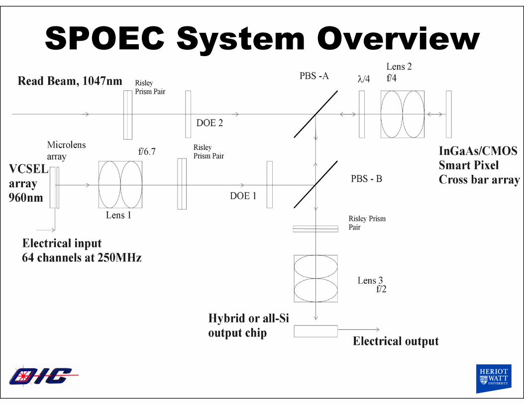
SPOEC System Overview
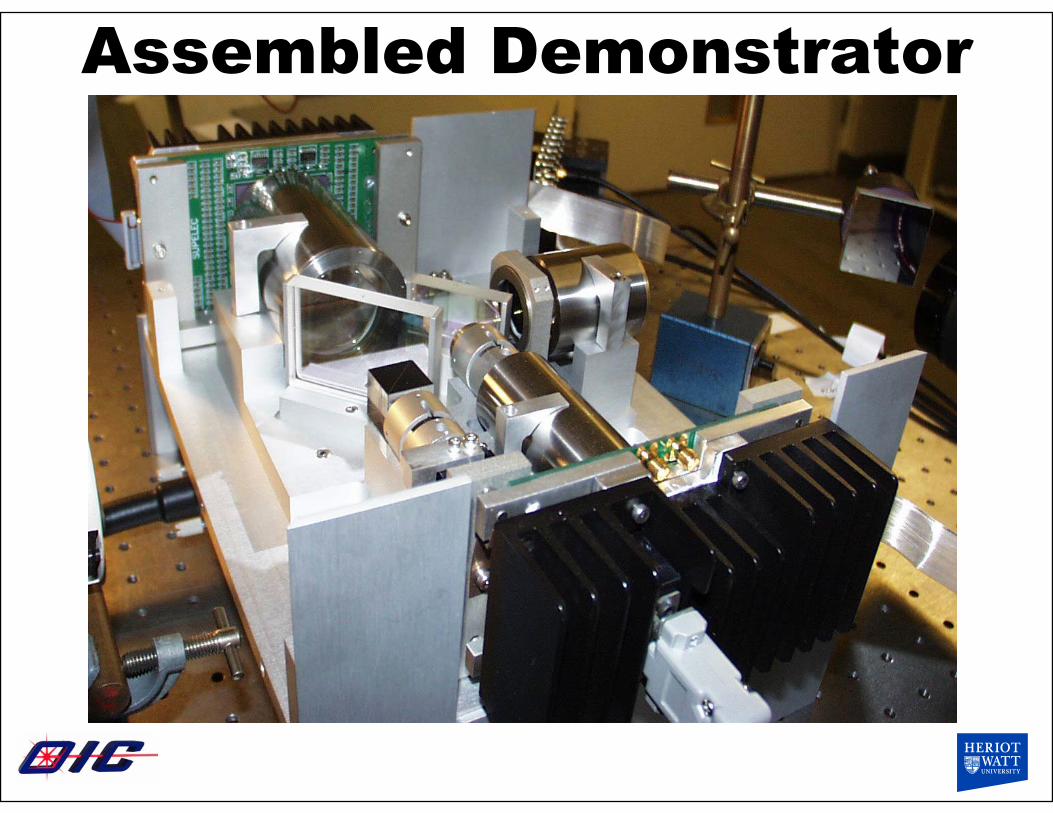
Assembled Demonstrator

Optoelectronic Neural Networks
• Neural networkscalability limited insilicon.
• Free-space optics can be used to perform interconnection.
• Optoelectronics allows scaleable networks.
• Input summation is also done in an inherently analogue manner.
• Noise added naturally.

Optical System
• DOE provides a shift invariant inhibitory interconnect pattern.• Neuron input summation is the total power falling on a detector.

System Overview

STAR Optical Chip Carrier• 4×4 device
constructed.• 16Gbs-1 aggregate
data rate. • Compressible
polymer bumps ease strain.
• Multimode waveguides.

Direct Write, Multi-level Waveguides

• “Optical wiring” capability for high density integration of active optoelectronic devices and packaging to parallel fibre I/O.
STAR 3D LightwaveCircuits

STAR 3DLC Test Waveguides
Waveguide Core Waveguide Cladding(upper & lower)
OECC substrate
Metallised 45ºpolymer surface
~100 µm
(A) (B) (C)
Output (coming out of plane of
paper)
Cladding
45º metallised polymer surface
used for lower mirror ~50µm(D) (E)
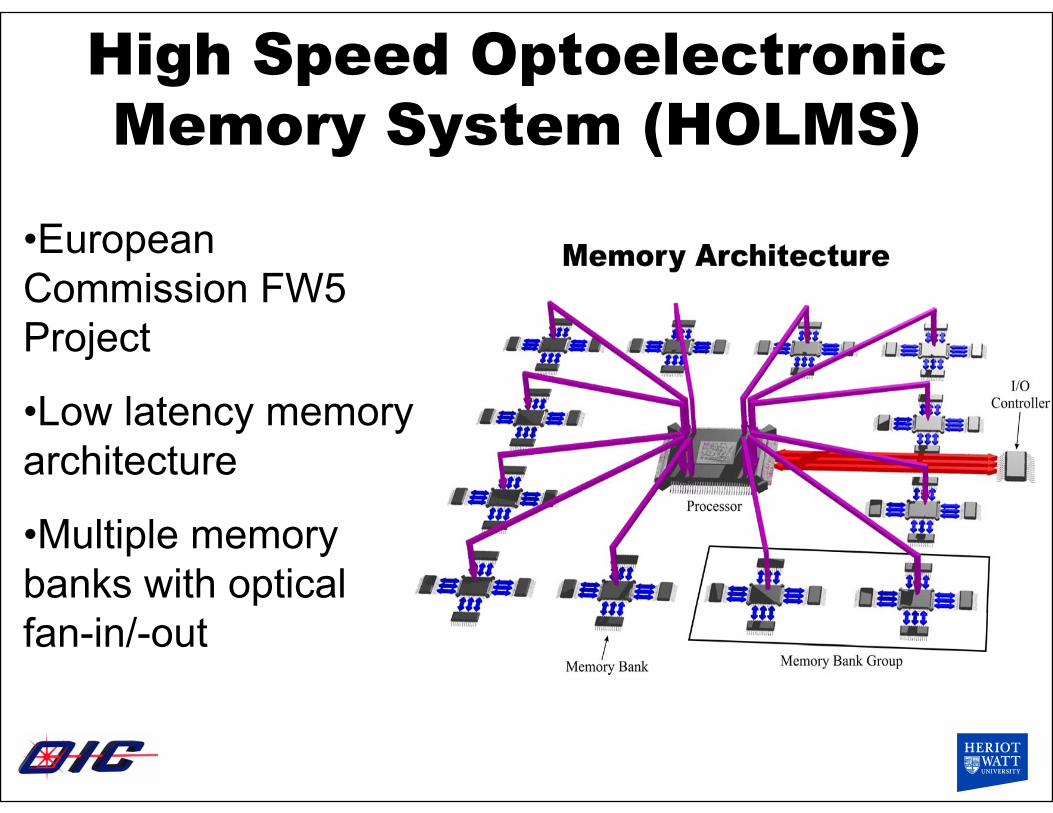
High Speed Optoelectronic Memory System (HOLMS)
•European Commission FW5 Project
•Low latency memory architecture
•Multiple memory banks with optical fan-in/-out

High Speed Optoelectronic Memory System (HOLMS)
•Test bed for multiple optical technologies and packaging
•Fibre
•PIFSO
•Waveguide

HOLMS MCM
Mixed Signal Chip Mixed Signal Chip
Detector Array
(1x12)
VCSEL Array
(1x12)

Programmable Optoelectronic Computing
Architecture (POCA)•Investigate reconfigurable logic (FPGAs) with optical I/O
•Logic required for data recovery and error recovery
•Latency for added logic
•Behavioural model of optoelectronic level for simulation

POCA 2
•Virtex 2 Pro @ 320MHz
•Rx -> Parity Check -> Input Buffer -> Output Buffer -> Parity Calc -> Tx
•165ns latency = 52 clock cycles

Technologies

Rapid prototyping of opto-mechanical structures
630nmDiode laser
PCB driver lasercontroller
Liquid Crystal Plate
Liquid Crystal Frame
Wired-Grid Polarizer usedas Polarizing Beam Splitter
PBS Frame Laser Frame
Structures has been made using a fast 3D printer which creates themodels directly from digital data in hours

Real system

Bonding• Direct epitaxial optical
I/O integration in its infancy.• Extra epitaxial layers
will decrease yield.• Thermal and voltage
issues critical at 90nm.• Cannot run optical I/O
off any less than 3.3V.
• Use flip-chip techniques instead until optical I/O epitaxyimproves.

Optoelectronic Packaging• FC6 flip-chip bonder for
• IR Thermocompression• UV Thermocompression• Reflow
• K&S 4124 ball bonder• EDB80 wire bonder
• Stud, die and wire bonding
• Access to facilities of specialist packaging companies for larger jobs

Solder Bumps• Pb/Sn solder phased out. Au/Sn and In bumps.• Creep rate can give micron level misalignment.• Flux required. Can lead to impurities in the process.

Gold Stud Bumps• Good conductor, requires no flux, no creep.• Only needs a modified wire bonder.• Needs higher temperature and pressure
than other attach methods.• Final attach uses either conductive adhesive
or reflow and pressure.

Anisotropic Conductive Film• Gold stud bumps formed and ACF used to create connection.• Connection formed by compression of conductive particles.• Resistivity varies from bond-site to bond-site.• Can only be used at lower speeds: <1GHz.

Compliant Polymer Bumps• Polymer bumps compressed to 80% original size to
make connection.• Bump elasticity gives tolerance to thermal mismatch.• Flip-chipped substrate glued in place.• Larger dimensions allow integrated waveguides.

Conclusions and Final Thoughts• Our experience of high connectivity free-space demonstrators• Opto-mechanical design important for any optical system
• Slotted base plate• Rapid prototyping
• Opto-electronic packaging• Our own small scale facilities and contacts with larger industrial
partners• Computer architecture as well as optical engineering expertise
• The Rest of Heriot-Watt University Physics• Diffractive Optics• Quantum Cryptography• Semiconductor Physics• ……….