Optically Interconnected Static-RAM for Instruction · PDF fileOptically Interconnected...
11
Optically Interconnected Static-RAM for Instruction Level Parallel Processors Dennis W. Prather, Michael L. Liccone, Marion LeCompte, Xiang Gao, Brian McMonagle, Richard Doyle, Paul R. Berger, and Sean Rommel The University of Delaware Department of Electrical and Computer Engineering 140 Evans Hall Newark, DE 19711 ABSTRACT In this paper we introduce a micro-optical architecture that uses meso-scopic diffractive optical elements ( DOEs) as three dimensional interconnects in a memory system for high level instruction level parallelism (ILP) processors. By using meso-scopic DOEs we can reduce the scale of integration to the VLSI scale, i.e., the micron scale, achieve submicron alignment tolerance, improve reliability due to monolithic integration, facilitate integration into the current manufacturing infrastructure, and offer the ability for higher bandwidth and high interconnect densities. To this the end we are developing the component technologies needed to realize this system. In this paper we present our work in the development of a theoretical and experimental framework for the design and characterization of meso-scopic DOEs, preliminary experimental results of meso-scopic beam splitters, and a large scale demonstration of the ILP memory system. 1. INTRODUCTION The perpetual demand to process more information in shorter time frames has resulted in a significant disparity between processor speeds and memory access times. In short, we can currently process data an order of magnitude faster than we can retrieve it. For instance, in the last ten years, CPU cycle times have dropped from around 3Ons (33MHz) to ins (1GHz), whereas in the same period of time, dynamic RAM cycle times have gone from l2Ons to 2Ons. Despite an attempt to circumvent this problem, by incorporating several megabytes of static random access memory (SHAM), or cache, in the processor, cycle times have only decreased to the neighborhood of iOns. Thus, the effective cost of accessing memory has still increased from four processor cycles to ten. This problem will be exacerbated with the advent of high level instruction level parallelism (ILP) central processing units (CPUs), or processors. An ILP processor is a single CPU that consists of as many as 6 to 8 functional units that all simultaneously execute instructions, or computations, during each clock cycle. Although in principle ILP processors offer significant advantages as compared to conventional processors the ability to realize their full potential is limited by I/O bottlenecks caused by relatively slow memory access times. In addition, in many cases, the data from one functional unit is needed in another in order for it to execute the next instruction; such a case is referred to as data dependency and gives rise to computational bottlenecks. In this situation, the distribution of data from a single functional unit to other functional units, at fractions of a clock cycle, is desired. For this reason a memory architecture that replicates the local memory for each functional unit and sends it to every other functional unit is needed. The distribution of data must occur at fractious of a Part of the SPIE Conference on Optoelectronic Interconnects VI San Jose, California • January 1999 309 SPIE Vol. 3632 • 0277-786X199/$lO.OO
Transcript of Optically Interconnected Static-RAM for Instruction · PDF fileOptically Interconnected...
Optically Interconnected Static-RAM for Instruction LevelParallel Processors
Dennis W. Prather, Michael L. Liccone, Marion LeCompte, Xiang Gao,Brian McMonagle, Richard Doyle, Paul R. Berger, and Sean Rommel
The University of DelawareDepartment of Electrical and Computer Engineering
140 Evans HallNewark, DE 19711
ABSTRACTIn this paper we introduce a micro-optical architecture that uses meso-scopic diffractive optical elements( DOEs) as three dimensional interconnects in a memory system for high level instruction level parallelism(ILP) processors. By using meso-scopic DOEs we can reduce the scale of integration to the VLSI scale, i.e.,the micron scale, achieve submicron alignment tolerance, improve reliability due to monolithic integration,facilitate integration into the current manufacturing infrastructure, and offer the ability for higher bandwidthand high interconnect densities. To this the end we are developing the component technologies needed torealize this system. In this paper we present our work in the development of a theoretical and experimentalframework for the design and characterization of meso-scopic DOEs, preliminary experimental results ofmeso-scopic beam splitters, and a large scale demonstration of the ILP memory system.
1. INTRODUCTIONThe perpetual demand to process more information in shorter time frames has resulted in a significantdisparity between processor speeds and memory access times. In short, we can currently process data anorder of magnitude faster than we can retrieve it. For instance, in the last ten years, CPU cycle times havedropped from around 3Ons (33MHz) to ins (1GHz), whereas in the same period of time, dynamic RAMcycle times have gone from l2Ons to 2Ons. Despite an attempt to circumvent this problem, by incorporatingseveral megabytes of static random access memory (SHAM), or cache, in the processor, cycle times haveonly decreased to the neighborhood of iOns. Thus, the effective cost of accessing memory has still increasedfrom four processor cycles to ten. This problem will be exacerbated with the advent of high level instructionlevel parallelism (ILP) central processing units (CPUs), or processors.
An ILP processor is a single CPU that consists of as many as 6 to 8 functional units that all simultaneouslyexecute instructions, or computations, during each clock cycle. Although in principle ILP processors offersignificant advantages as compared to conventional processors the ability to realize their full potential islimited by I/O bottlenecks caused by relatively slow memory access times. In addition, in many cases, thedata from one functional unit is needed in another in order for it to execute the next instruction; such acase is referred to as data dependency and gives rise to computational bottlenecks. In this situation, thedistribution of data from a single functional unit to other functional units, at fractions of a clock cycle, isdesired. For this reason a memory architecture that replicates the local memory for each functional unitand sends it to every other functional unit is needed. The distribution of data must occur at fractious of a
Part of the SPIE Conference on Optoelectronic Interconnects VISan Jose, California • January 1999 309SPIE Vol. 3632 • 0277-786X199/$lO.OO
310
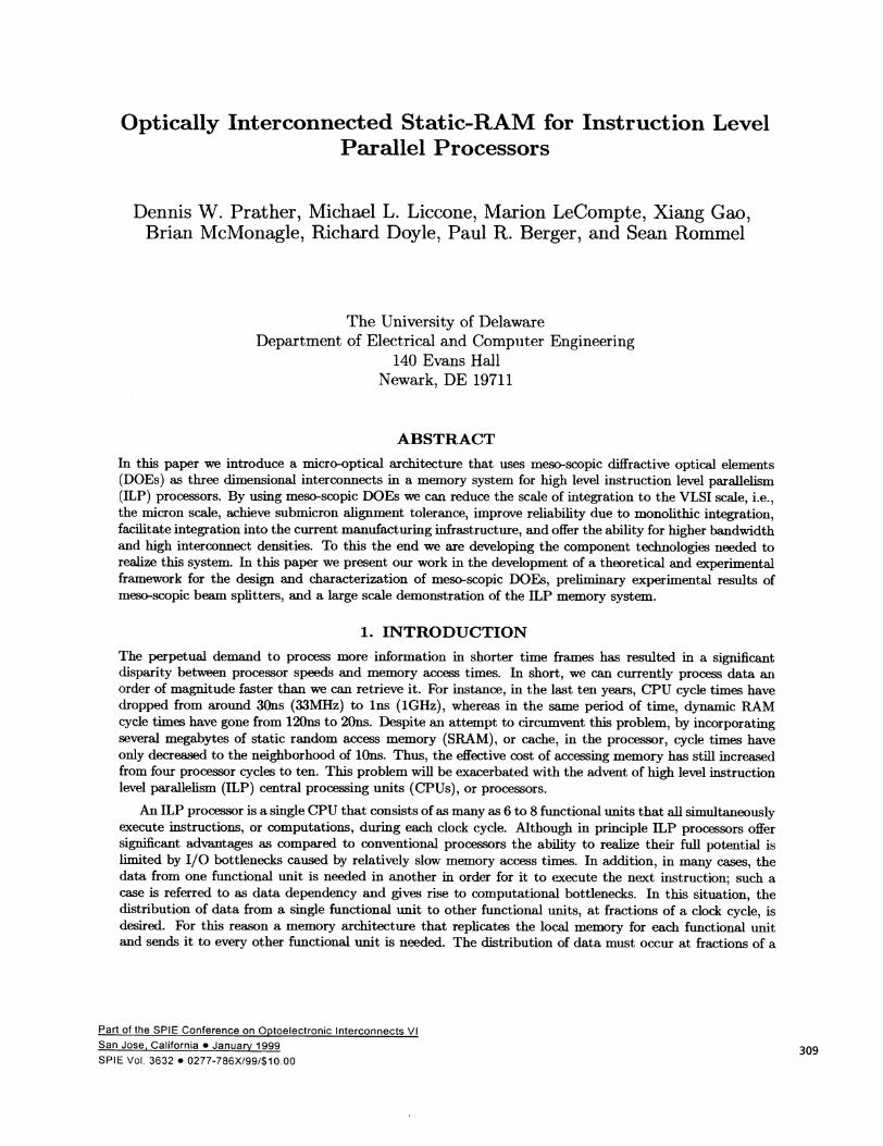
microns
Figure 1. Illustratioii of a micron scalel—to—5 fan—out DOE, computed using the bondary eleiiient Inetllo(l.
clock cycle in order to insure that the data contained n meniory is available to au alternate functional iuutshould it he needed for the next clock cycle.
Because an all electronic solution to this problem is difficult, we propose the (lesign of an optical intercon--nect architecture that incorporates data redundancy by fanning out the data from a giveli functional unit toas many as 16 to 32 other functional units. The key to this architecture is the use of vertical cavity surfaceemitting laser (VCSEL) arrays and their integration with nieso—scopic DOEs in order to distribute, or redi--rect, data to receivers located at neighboring functional units. Each communication channel in our (lesigilwill consume approximately 50mW of power which when applied to a full 16 x 16 interconnection (worstcase scenario) would consume on the order of 10 Watts of power, which is nearly au order of niagnitude lessthan current architectures that are limited to at most 4 x 4 interconnections.
In order to realize such optical interconnections on a single silicon die one must. he able to integrate activeand passive optical devices together on the microelectronics scale, while preserving the ability to controland redirect light in a general fashion, e.g., off-axis focusing and beam fan-out. Whereas active opticaldevices, such as eniitters, detectors, arid modulators are readily designed and fabricated with dimensionson the nhicron scale,1 5 until recently passive optical elenients, capable of such general behavior, were not.However, recent advances iii both the design613 and fabrication'4'7 of diffractive structures iiow enablethe integration of active and passive optical devices on the micron scale and the abilit.y to efficiently controland redirect light in a general fashion, see Fig L Thus, the integration of VCSELs with wavelength scalefan-out, DOEs on the VLSI scale offer not only an order of magnitude improvement (in terms of latencyand lower consumption) in current ILP architectures hut also the ability to design ILPs that heretoforehave not been possible. In the course of this paper we discuss our design and analysis methods for meso-scale DOEs, present preliminary experimental results for the fanning out of data on tile meso-scale, an(l thedemonstration of a large scale ILP memory system.
2. ARCHITECTURE\Vherea.s the use of optical interconnects in long haul and local area networks has proven extremely successful,its use on the VLSI scale has been limited. This is due in large part to the continual increase in sl)eed andperformance in conventional electronic devices. However, the issues associated with next generation ILPprocessors cannot be adequately addressed with speed alone. Instead, such processors will require not onlythe ability to share or distribute information among processing units (signal fan—out) but also a significantincreases in interconnect density. 'While the issues of increased bandwidth, int.ercomiect densities, and signalfan—out are individually compelling reasons for considering optical iiiterconnects, when combined togetherthey become persuasive. For example, one possible electronic solution to increasing interconnect (lensity is
-300 -200 -100 0 100 200 300
microns
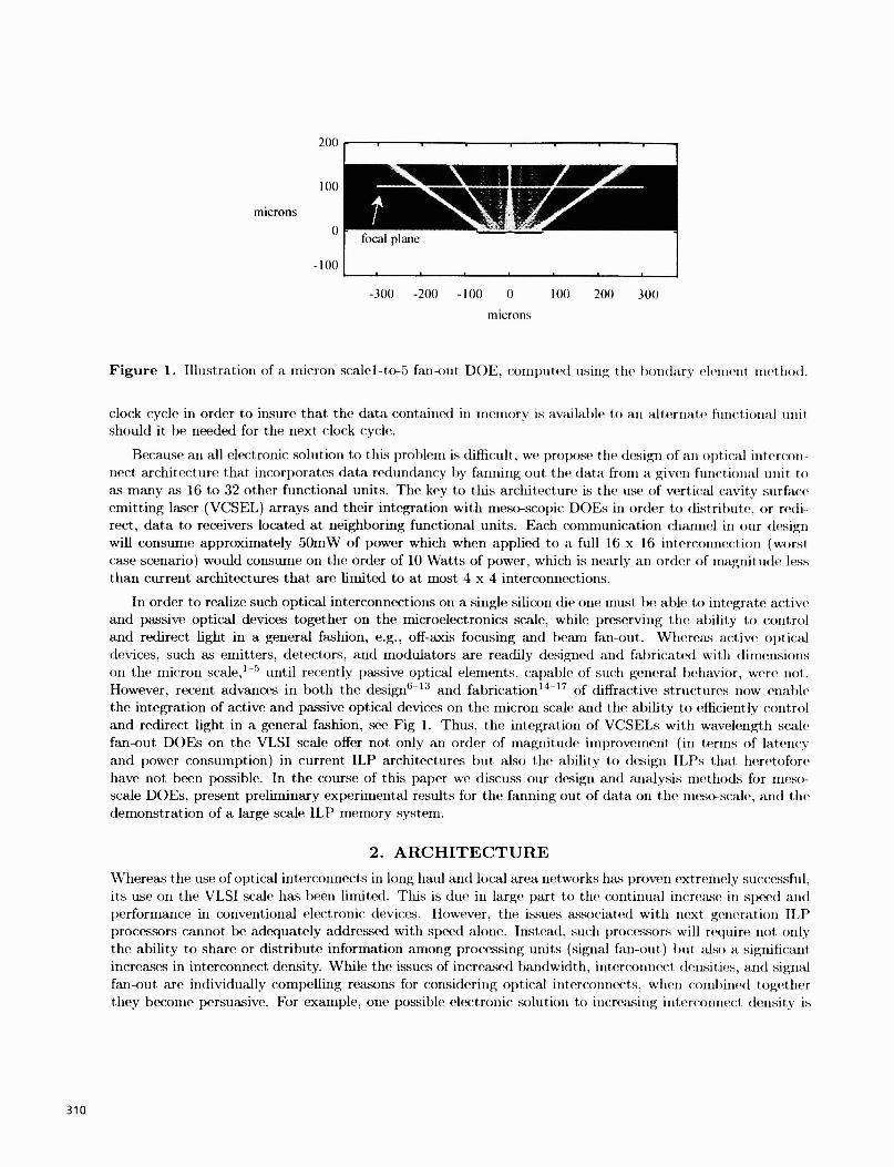
DOEs
VCSEL98Onm- l3Thi
I)eteclors (CMOS.SiGe, or GaAs)
Figure 2. Monolithic architecutre that uses 3D optical interconiiects on the meso-scopic scale,FU=functional unit, MEM=memory, x=VCSEL, and o=detector.
to use flip-chip, or bump, bonds, which require approximately 20 m2 of chip area while offering only a1-to-i interconnect. In comparison, meso-scopic DOEs can be designed to provide more than an order ofmagnitude increase in interconnect density within the same area, as discussed in Sec. 3. For this reason wepropose the use of a 3D optical interconnect architecture that uses monolithically integrated lileso-scopicDOEs on a VLSI scale for application to ILP processors, as shown in Fig. 2.
In this architecture the memory circuits are all electronic and the optical interconnects are used only tofan-out and distribute data among the various functional units, which are also all electronic. To this end, weenvision the DOEs to be fabricated directly in the silicon substrate immediately adjacent to VLSI circuits.Active devices such as one- or two-dimensional VCSEL arrays are flip-chip bonded onto CMOS (Irivers andassuming a long enough wavelength (greater than 1.0(Lm) they can be (lirected through a DOE and usethe silicon substrate as the propagating medium. If possible the detectors will he fabricated monolithically,however, this would require VCSEL wavelengths that are below 1.Oitm. Alternatively, SiGe5 or GaAs18"9detectors could be used for longer wavelength VCSELs. IS shorter wavelength VCSELs were used (980n'ni)then either the silicon substrate would have to be thinned, to reduce the attenuation of the optical beams,or a transparent and insulating substrate could be used, such as Si02.
This architecture offers the following advantages: (1) scale of integration, i.e., the micron scale, 25preserved. (2) aliqnment tolerance is subrnicron, (9) high reliability due to single substrate integration, (4)easily integrates into the current manufacturing infrastructure, and (5) offers the ability for higher bandwidthand interconnect densities. Although we are in the initial stages of this effort we have began (leveloping thekey technologies that are required to enable the realization of this system. They include the development ofelectromagnetic analysis methods for DOEs, experimental characterization of Irieso—scopic DOEs, and novelmemory architectures. In the remainder of this paper we discuss our progress in each of these areas.
311
VLSI (memory.drivers. receivers)
312
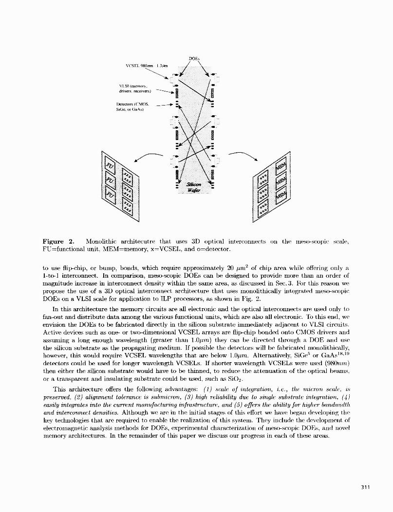
off-axisfocus
diffractive lens \ fabrication" window
xo
off-axisshift
Figure 3. Design of an off-axis diffractive lens by selecting a subsection from a full lens proffle.
3. DIFFRACTIVE OPTICAL ELEMENTSIn this section we discuss the design and analysis of meso-scopic DOEs for application to ILP processors.As shown in Fig. 2 the principle role of DOEs in this architecture is to distribute light from a single sourceto an array of corresponding detectors. Whereas conventional methods for distributing light using DOEs2°are well known, they have been shown to breakdown as the scale of the DOE approaches the wavelength.21This occurs because such methods are based on scalar diffraction theory, which is not valid on this scale.To overcome this limitation we have designed our beam splitters as arrays of off-axis lenses. In this casethe incident field is redirected to a given detector depending on the particular segment of the DOE that itilluminates.
The design of our off-axis lens array is determined by creating a fabrication window within the proffle of acomplete diffractive lens, the center of which is given by x0 as shown in Fig. 3. The center of the window, x0,is chosen such that the center of the incident field over that region is focused onto a corresponding detector.For a one-dimensional proffle the phase of a diffractive lens is given by,
2irçb(x) =- — x)2 + f2 —
A mod 2x
where and the off-axis angle, Ooffaxis is defined as
—1 Ixof—axis = tan
A critical parameter in the design of an off-axis lens is the maximum off-axis angle, which is limited bythe minimum zone width, d, and is given by,
ASmOoffaxjs =
This correspondingly determines the f/# of the full lens proffle from which the off-axis lens is designed,through the relation
1
29off—axis +
When the feature size in the off-axis lens becomes comparable iii scale to the illumination wavelength tradi-tional methods used to analyze their performance become invalid, such as scalar diffraction theory. In thesecases it is necessary to rigorously solve the electromagnetic boundary value problem using a more rigoroustechnique. To his end we have developed several rigorous methods that use numerical electromagnetictechniques22 to solve for the diffraction from meso-scopic DOEs.13
The method that we used to design the DOEs presented above is based on the finite-difference time-domain method (FDTD). In this method Maxwell's equations, in differential form, are approximated asdifference equations and evaluated through the time marching algorithm.22'23 This method has several ad-vantages in comparison to alternate electromagnetic metho&3 in that it does not require the solution ofa large system of equations and requires far less memory. Using this technique we designed a lens and twosplitters on the meso-scale. In the next section we discuss their experimental characterization.
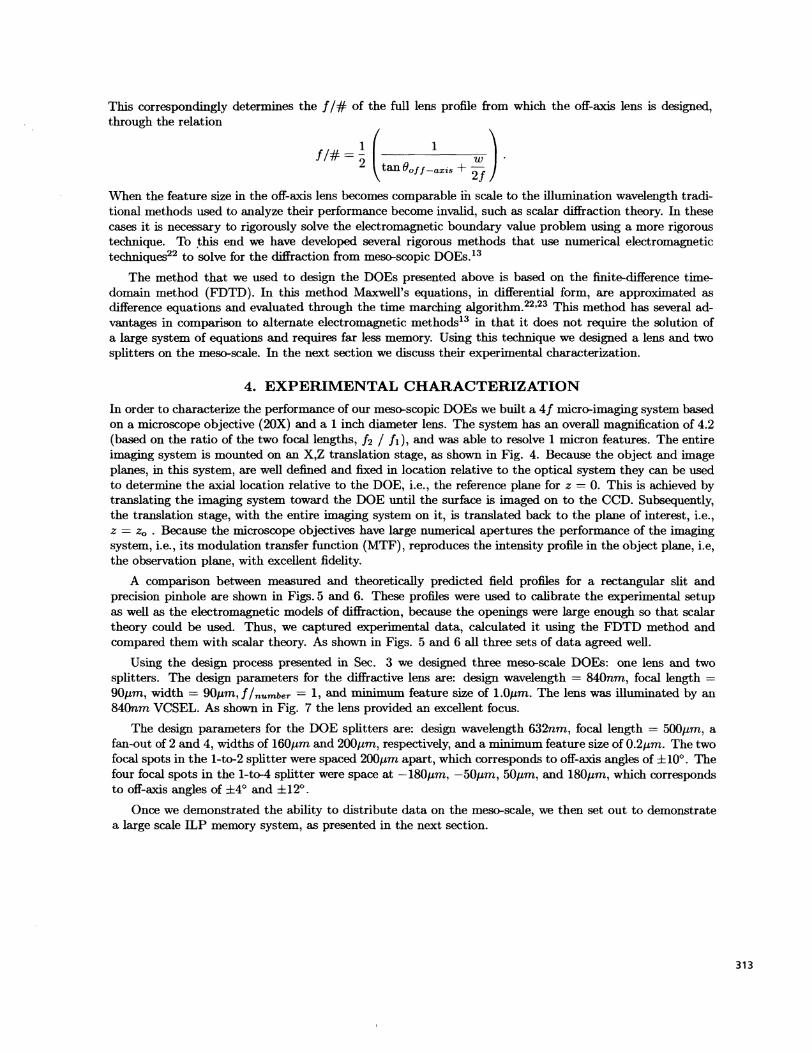
4. EXPERIMENTAL CHARACTERIZATIONIn order to characterize the performance of our meso-scopic DOEs we built a 4f micro-imaging system basedon a microscope objective (20X) and a 1 inch diameter lens. The system has an overall magnification of 4.2(based on the ratio of the two focal lengths, f2 I fi), and was able to resolve 1 micron features. The entireimaging system is mounted on an X,Z translation stage, as shown in Fig. 4. Because the object and imageplanes, in this system, are well defined and fixed in location relative to the optical system they can be usedto determine the axial location relative to the DOE, i.e., the reference plane for z = 0. This is achieved bytranslating the imaging system toward the DOE until the surface is imaged on to the CCD. Subsequently,the translation stage, with the entire imaging system on it, is translated back to the plane of interest, i.e.,z = z0 . Because the microscope objectives have large numerical apertures the performance of the imagingsystem, i.e., its modulation transfer function (MTF), reproduces the intensity profile in the object plane, i.e,the observation plane, with excellent fidelity.
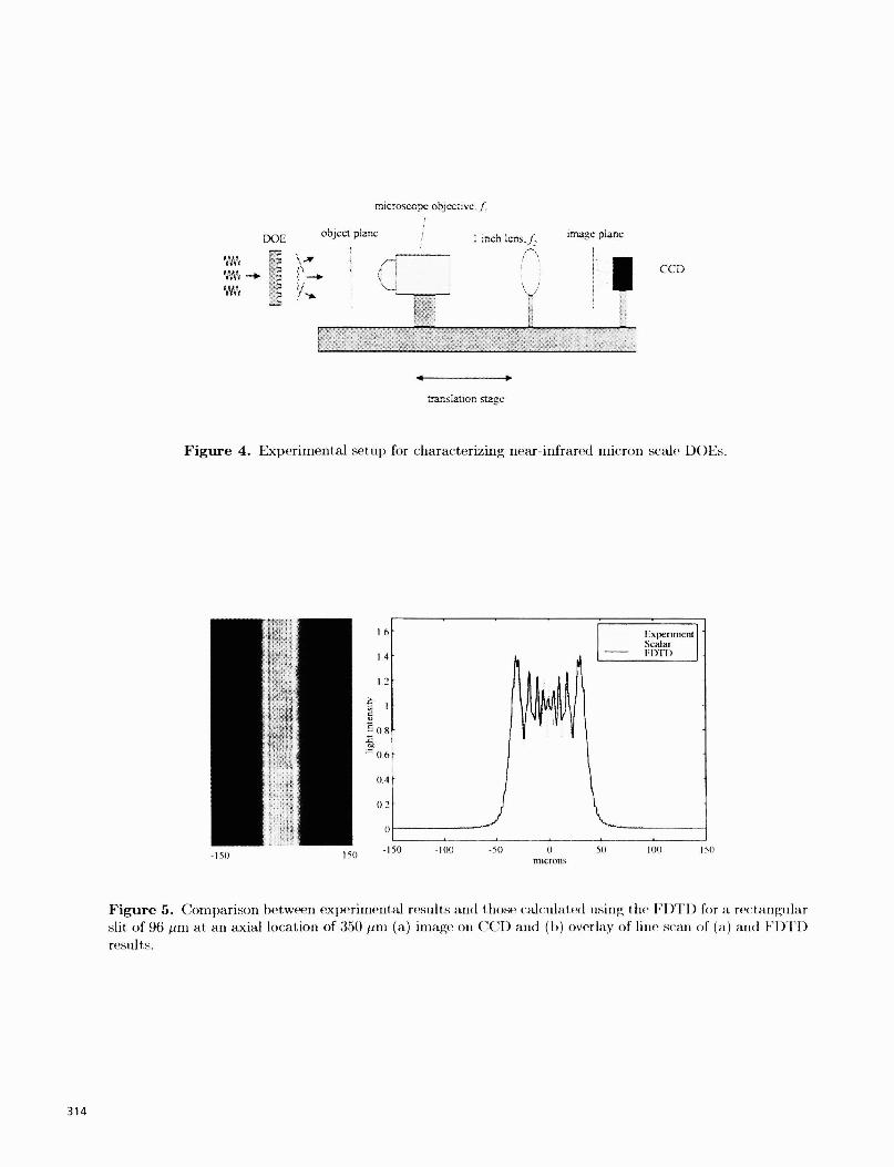
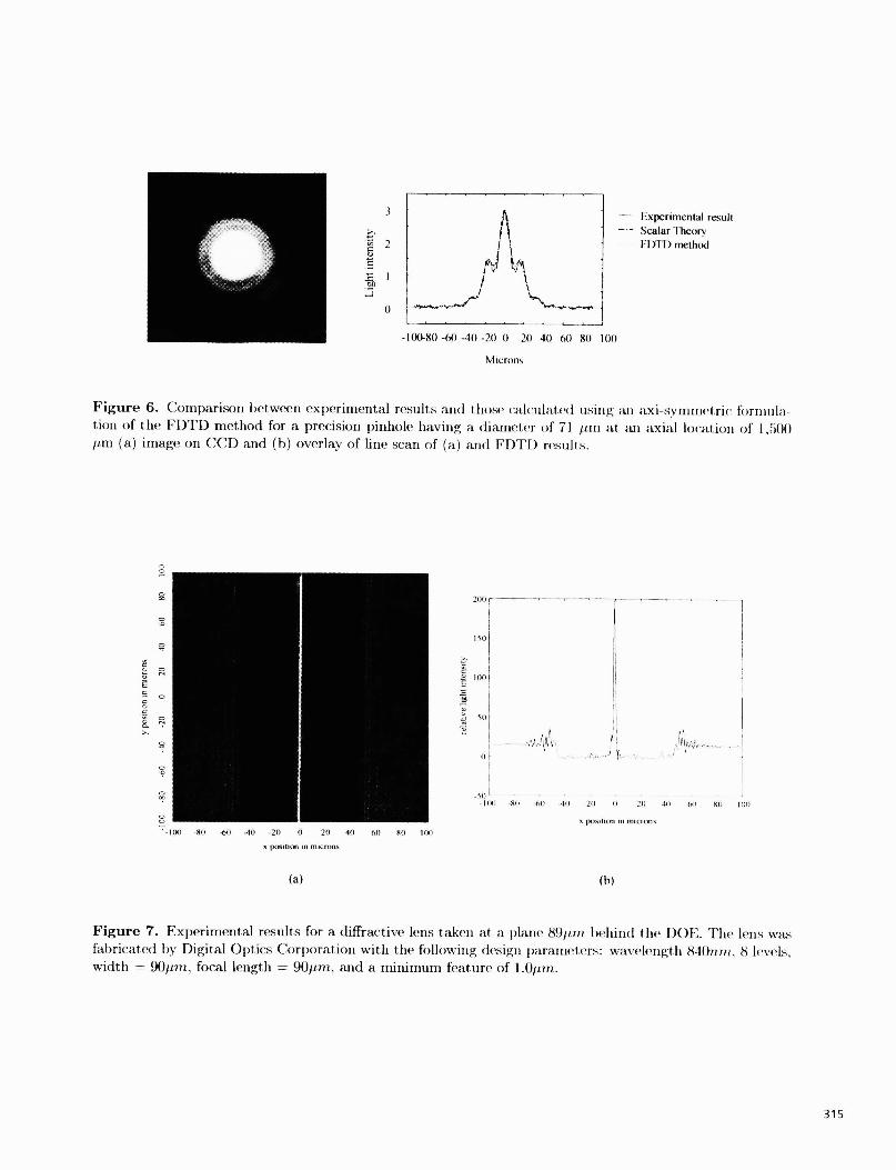
A comparison between measured and theoretically predicted field proffles for a rectangular slit andprecision pinhole are shown in Figs. 5 and 6. These proffles were used to calibrate the experimental setupas well as the electromagnetic models of diffraction, because the openings were large enough so that sca1artheory could be used. Thus, we captured experimental data, calculated it using the FDTD method andcompared them with scalar theory. As shown in Figs. 5 and 6 all three sets of data agreed well.
Using the design process presented in Sec. 3 we designed three meso-scale DOEs: one lens and twosplitters. The design parameters for the diffractive lens are: design wavelength =840nm, focal length =9Om, width = 9Ojm, f/number 1, and minimum feature size of 1.Oim. The lens was illuminated by an840nm VCSEL. As shown in Fig. 7 the lens provided an excellent focus.
The design parameters for the DOE splitters are: design wavelength 632nm, focal length = 5OOtm, afan-out of 2 and 4, widths of l6Opm and 2OOm, respectively, and a minimum feature size of O.2tm. The twofocal spots in the 1-to-2 splitter were spaced 2OOtm apart, which corresponds to off-axis angles of Thefour focal spots in the 1-to-4 splitter were space at --l8Opm, —50jim, 50jm, and 18Ojm, which correspondsto off-axis angles of and
Once we demonstrated the ability to distribute data on the meso-scale, we then set out to demonstratea large scale ILP memory system, as presented in the next section.
313
314
anslation stage
Figure 4. Experimental setup for characterizing near-infrared micron scale DOEs.
150
Figure 5. Coiriparison between experimental results and t hose calculated using the l1)T1) fur a rectangularslit of 96 izni at an axial location of 35() irii (a) image on CCI) and (h) overlay of line scan of (a) and FIJIDresults.
DOE object plane
11t
microscope objcctve.f,
I inch Icnsf un plane
CCD
___________ /
I)
Figure 6. Comparison I)et.ween experimental results and those cal(lllate(I using an axi—syitirtietrir hrinula-tion of t lie FI)TD method for a precision pinhole having a diairieter of 71 at an axial location of I ,5t)()im (a) image on CCD and (h) overlay of line scan of (a) arid FDTD results.
Is000F
I I
Figure 7. Experimental results for a diffractive lens taken at a plane 89jiiii heliiiid the l)OE. The lens wasfabricated by Digital Optics Corporation with the following (lesigli I)araIntt(rs: waveleiigtli S-lDnin. S leveLs,width = 9Otin, focal length 9Oitm, and a minimum feature of 1.Oim.
3
A
0
Ixpcrimental result— - Scalar theory
mn) method
— I 00—80 —64) —40 —20 0 20 40 60 80 100
Microns
0
a
a
SI)
-101) -8)) -.60 -40 -20 0 21) 40 60 80 0))
position in microns
-so- IS) —8)) —1,)) —4)) -20 1) () 40 1,)) 6))
S JXiSiliOTi iii fliiCiifliS
(a) (h)
315
316
(a) (b)
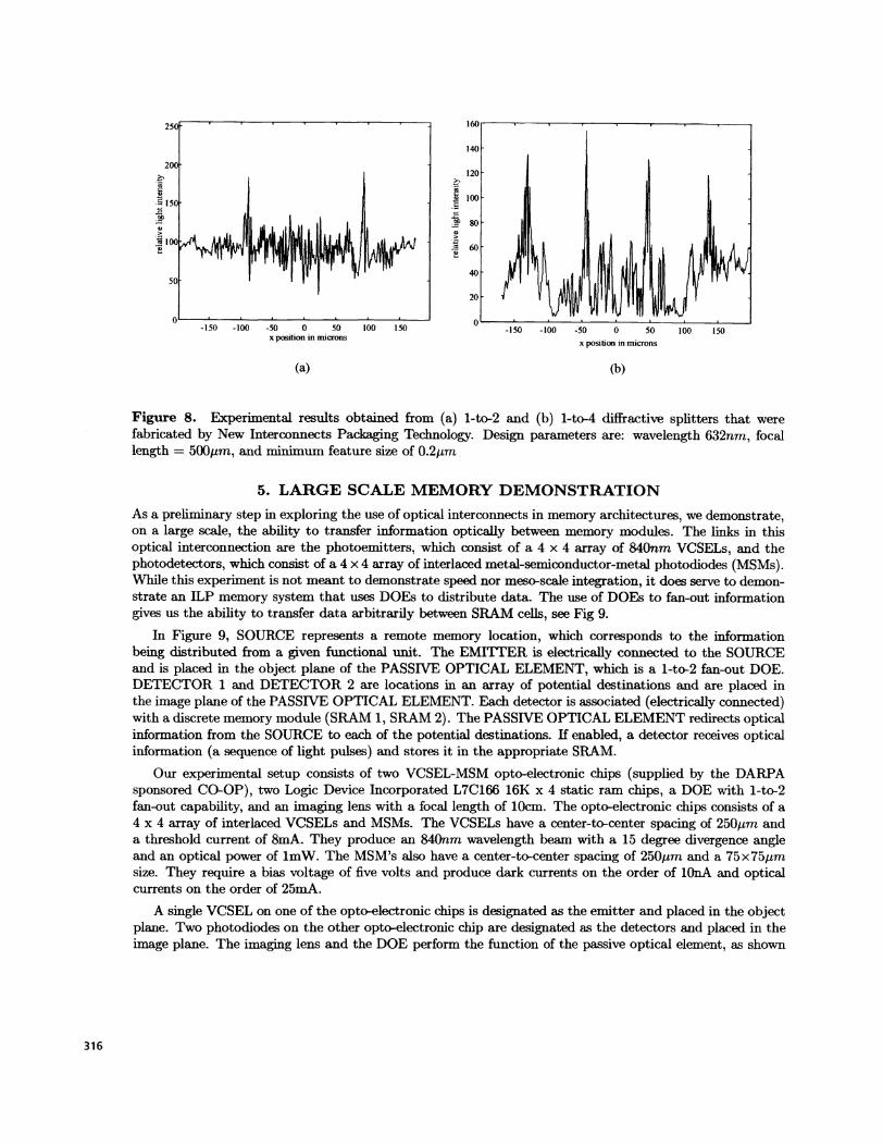
Figure 8. Experimental results obtained from (a) 1-to-2 and (b) 1-to-4 diffractive splitters that werefabricated by New Interconnects Packaging Technology. Design parameters are: wavelength 632nm, focallength = 500jim, and minimum feature size of O.2m
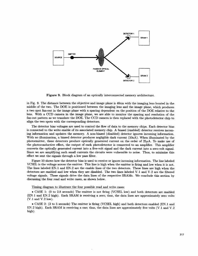
5. LARGE SCALE MEMORY DEMONSTRATIONAs a preliminary step in exploring the use of optical interconnects in memory architectures, we demonstrate,on a large scale, the ability to transfer information optically between memory modules. The links in thisoptical interconnection are the photoemitters, which consist of a 4 x 4 array of 840nm VCSELs, and thephotodetectors, which consist of a 4 x 4 array of interlaced metal-semiconductor-metal photodiodes (MSMs).While this experiment is not meant to demonstrate speed nor meso-scale integration, it does serve to demon-strate an ILP memory system that uses DOEs to distribute data. The use of DOEs to fan-out informationgives us the ability to transfer data arbitrarily between SRAM cells, see Fig 9.
In Figure 9, SOURCE represents a remote memory location, which corresponds to the informationbeing distributed from a given functional unit. The EMITTER is electrically connected to the SOURCEand is placed in the object plane of the PASSIVE OPTICAL ELEMENT, which is a 1-to-2 fan-out DOE.DETECTOR 1 and DETECTOR 2 are locations in an array of potential destinations and are placed inthe image plane of the PASSIVE OPTICAL ELEMENT. Each detector is associated (electrically connected)with a discrete memory module (SRAM 1, SRAM 2). The PASSIVE OPTICAL ELEMENT redirects opticalinformation from the SOURCE to each of the potential destinations. If enabled, a detector receives opticalinformation (a sequence of light pulses) and stores it in the appropriate SHAM.
Our experimental setup consists of two VCSEL-MSM opto-electronic chips (supplied by the DARPAsponsored CO-OP), two Logic Device Incorporated L7C166 16K x 4 static ram chips, a DOE with 1-to-2fan-out capability, and an imaging lens with a focal length of 10cm. The opto-electronic chips consists of a4 x 4 array of interlaced VCSELs and MSMs. The VCSELs have a center-to-center spacing of 25Om anda threshold current of 8mA. They produce an 840mm wavelength beam with a 15 degree divergence angleand an optical power of 1mW. The MSM's also have a center-to-center spacing of 250,um and a 75 x 75tmsize. They require a bias voltage of five volts and produce dark currents on the order of lOnA and opticalcurrents on the order of 25mA.
A single VCSEL on one of the opto-electronic chips is designated as the emitter and placed in the objectplane. Two photodiodes on the other opto-electronic chip are designated as the detectors and placed in theimage plane. The imaging lens and the DOE perform the function of the passive optical element, as shown
-150 -100 -50 0 50 100 150xposition in microns
x position in microns
D€TECTOR I
Figure 9. Block diagram of an optically interconnected memory architecture.
in Fig. 9. The distance between the objective and image plane is 40cm with the imaging lens located in themiddle of the two. The DOE is positioned between the imaging lens and the image plane, which producesa two spot fan-out in the image plane with a spacing dependent on the position of the DOE relative to thelens. With a CCD camera in the image plane, we are able to monitor the spacing and resolution of thefan-out pattern as we translate the DOE. The CCD camera is then replaced with the photodetector chip toalign the two spots with the corresponding detectors.
The detector bias voltages are used to control the flow of data to the memory chips. Each detector biasis connected to the write enable of its associated memory chip. A biased (enabled) detector receives incom-ing information and updates the memory. A non-biased (disabled) detector ignores incoming information.With no illumination, a biased detector produces negligible dark current (lOnA). When illuminated by thephotoernitter, these detectors produce optically generated current on the order of 25jiA. To make use ofthe photoconductive effect, the output of each photodetector is connected to an amplifier. This amplifierconverts the optically generated current into a five-volt signal and the dark current into a zero-volt signal.Since we are amplifying such small currents the circuits were vulnerable to noise. Thus, to minimize thiseffect we sent the signals through a low pass filter.
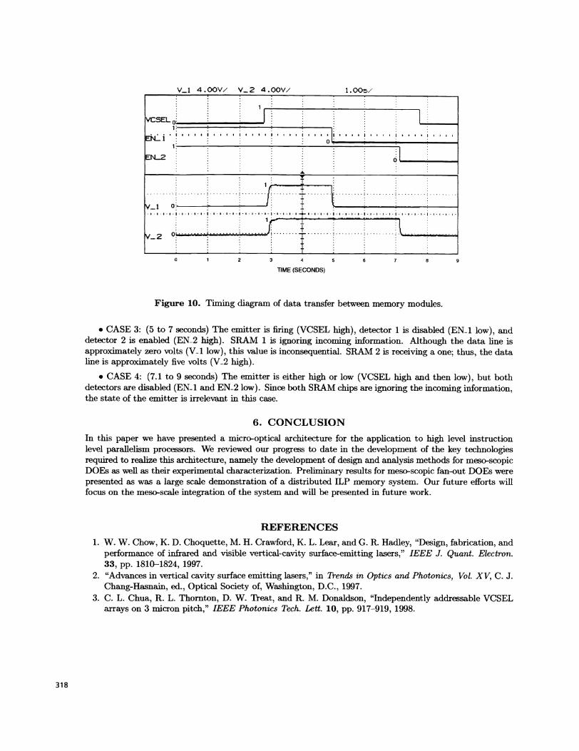
Figure 10 shows how the detector bias is used to receive or ignore incoming information. The line labeledVCSEL is the voltage across the emitter. This line is high when the emitter is firing and low when it is not.The lines labeled EN1 and EN2 are the enable lines of the two detectors. These lines are high when thedetectors are enabled and low when they are disabled. The two lines labeled V1 and V2 are the ifiteredvoltage signals. These signals drive the data lines of the respective SRAMs. We conclude this section bydiscussing the four read and write cases, as shown below.
Timing diagram to illustrate the four possible read and write cases:
• CASE 1: (0 to 2.8 seconds) The emitter is not firing (VCSEL low) and both detectors are enabled(EN1 and EN2 high). Each SHAM is receiving a zero; thus, the data lines are approximately zero volts(VA and V2 low).
• CASE 2: (3 to 5 seconds) The emitter is firing (VCSEL high) and both detectors enabled (ENA andEN2 high). Each SHAM is receiving a one; thus, the data lines are approximately five volts (VA and V2high).
317
OPTKAL5.BENT
OTECTOR 2
V_i 4. OOV/ V_ 2 4. OOV/ 1. OO/
VCSELO_____ LE L_.
E\L..''ENL_2 :
,.,,.,,$ I,,.,1____________
?_ 2
.
0 1 2 3 4 5 6 7 6 9
318
liME (SECONDS)
Figure 10. Timing diagram of data transfer between memory modules.
. CASE 3: (5 to 7 seconds) The emitter is firing (VCSEL high), detector 1 is disabled (ENi low), anddetector 2 is enabled (EN2 high). SRAM 1 is ignoring incoming information. Although the data line isapproximately zero volts (VJ low), this value is inconsequential. SRAM 2 is receiving a one; thus, the dataline is approximately five volts (V2 high).
S CASE 4: (7.1 to 9 seconds) The emitter is either high or low (VCSEL high and then low), but bothdetectors are disabled (EN..i and EN.2 low). Since both SRAM chips are ignoring the incoming information,the state of the emitter is irrelevant in this case.
6. CONCLUSIONIn this paper we have presented a micro—optical architecture for the application to high level instructionlevel parallelism processors. We reviewed our progress to date in the development of the key technologiesrequired to realize this architecture, namely the development of design and analysis methods for meso—scopicDOEs as well as their experimental characterization. Preliminary results for meso—scopic fan—out DOEs werepresented as was a large scale demonstration of a distributed ILP memory system. Our future efforts willfocus on the meso—scale integration of the system and will be presented in future work.
REFERENCESi. W. W. Chow, K. D. Choquette, M. H. Crawford, K. L. Lear, and G. R. Hadley, "Design, fabrication, and
performance of infrared and visible vertical-cavity surface—emitting lasers," IEEE J. Quant. Electron.33, pp. i810—1824, 1997.
2. "Advances in vertical cavity surface emitting lasers," in Thend in Optics and Photonics, Vol. XV, C. J.Chang-Hasnain, ed, Optical Society of, Washington, D.C., 1997.
3. C. L. Chua, It. L. Thornton, D. W. 'heat, and R. M. Donaldson, "Independently addressable VCSELarrays on 3 micron pitch," IEEE Photonics Tech. Lett. 10, pp. 917—919, 1998.
4. S. Q. Luong, G. G. Ortiz, Y. Zhou, J. Lu, C. P. Hams, J. Cheng, H. Q. Hou, and G. A. Vawter,"Monolithic wavelength-graded VCSEL and res()nance-elthanced photodetector arrays for parallel opti-cal interconnects," IEEE Photon. Tech. Lett. 10, pp. 642—644, 1998.
5. J. S. Rieh, D. Klotzkin, 0. Qasaimeh, L. H. Lu, K. Yang, L. P. B. Katehi, P. Bhattacharya, and E. T.Croke, "Monolithically integrated SiGe-si PIN--HBT front-end photoreceivers," IEEE Photon. Tech.Lett. 10, pp. 415—417, 1998.
6. D. W. Prather, M. S. Mirotznik, and J. N. Malt, "Boundary element method for vector modelingdiffractive optical elements," in Diffractive and Holographic Optics Technology II, I. Cindrich and S. H.Lee, eds., vol. 2404 of Proc. SPIE, pp. 28—39, 1995.
7. K. Hirayama, E. N. Glytsis, T. K. Gaylord, and D. W. Wilson, "Rigorous electromagnetic analysis ofdiffractive cylindrical lenses," J. Opt. Soc. Am. A 13, pp. 2219—2231, 1996.
8. D. W. Prather, M. S. Mirotznik, and J. N. Malt, "Boundary integral methods applied to the anaiysisof diffractive optical elements," J. Opt. Soc. Am. A 14, pp. 34—43, 1997.
9. D. W. Prather, J. N. Malt, M. S. Mirotznik, and J. P. Collins, "Vector-based synthesis of finite aperiodicsubwavelength diffractive optical elements," J. Opt. Soc. Am. A 15, pp. 1599—1607, 1998.
10. D. W. Prather, S. Shi, M. S. Mirotznik, and J. N. Mait, Vector-based analysis of axially-symmetricDOEs using the method of moments. 1998 OSA Topical Meeting on Diffractive Optics, Kona, HI.
11. D. W. Prather and S. Shi, "Formulation and application of the finite-difference time-domain methodfor the analysis of axially-symmetric DOEs," J. Opt. Soc. Am. A , (1999) accepted for publication.
12. D. W. Prather, S. Sin, and J. S. Bergey, "A field stitching algorithm for the analysis of electrically largefinite aperiodic diffractive optical elements," Opt. Lett. 24, March 1999. to appear.
13. D. W. Prather, M. S. Mirotznik, and S. Sin, Mathematical Modeling in Optical Science, ch. Electromag-netic models for finite aperiodic diffractive optical elements, p. in print. SIAM Frontier Book Series,Society for Industrial and Applied Mathematics, 1999.
14. D. Zaleta, W. Daschner, M. Larsson, B. C. Kress, J. Fan, K. S. Urquhart, and S. H. Lee, DiffractiveOptics Fabricated by Electron-Beam Direct Write Methods, vol. CR 49, pp. 117-137. SPIE Press, 1993.
15. M. Ekberg, F. Nikolajeff, M. Larsson, and S. Hard, "Proximity-compensated blazed transmission gratingmanufacture with direct-write electron-beam lithography," Appi. Opt. 33,pp. 103—107, 1994.
16. S. Y. Chou, P. R. Krauss, and P. J. Renstrom, "Imprint lithography with 25-nanometer resolution,"Science 272, pp. 85—87, 1996.
17. P. D. Maker, D. W. Wilson, and R. E. Muller., "Fabrication and performance of optical interconnectanalog phase holograms made by electron beam lithography," in Optoelectronic Interconnects and Pack-aging, R. T. Chen and P. S. Guilfoyle, eds., vol.. CR 62 of Proc. SPIE, pp. 415-430, 1996.
18. K. H. Calhoun, C. B. Camperi-Ginestet, and N. M. Jokerst, "Vertical optical communication throughstacked silicon wafers using hybrid monolithic thin film InGaAsP emitters and detectors," IEEE Photon.Technol. Lett. 5, pp. 254—257, 1993.
19. S. M. Fike, B. Buchanan, N. M. Jokerst, M. A. Brooke, T. G. Morris, and S. P. DeWeerth, "8 x 8 arrayof thin-film photodetectors vertically electrically interconnected to silicon circuitry," IEEE Photon.Technol. Lett. 7, pp. 1168—1170, 1995.
20. J. N. Mait, Micro-Optics, Elements, Systems and Applications, ch. Fourier Array Generators, pp. 293—324. Taylor and Francis, 1997.
21. E. Sidick, A. Knoesen, , and J. N. Mait, "Design and rigorous analysis of high-efficiency array genera-tors," Appi. Opt. 32, pp. 2599—2605, 1993.
22. M. N. Sadiku, Numerical Techniques in Electromagnetics, CRC Press, Boca Raton FL, 1992.23. A. Tafiove, Computational Electromagnetics: The Finite-Difference Time Domain Method, Artech
House, Boston MA, 1995.
319