Optical waveguide amplifiers based on Er-doped phosphate ...Optical waveguide amplifiers based on...
111
Optical waveguide amplifiers based on Er-doped phosphate glasses Citation for published version (APA): Yan, Y. C. (1997). Optical waveguide amplifiers based on Er-doped phosphate glasses. Eindhoven: Technische Universiteit Eindhoven. https://doi.org/10.6100/IR493128 DOI: 10.6100/IR493128 Document status and date: Published: 01/01/1997 Document Version: Publisher’s PDF, also known as Version of Record (includes final page, issue and volume numbers) Please check the document version of this publication: • A submitted manuscript is the version of the article upon submission and before peer-review. There can be important differences between the submitted version and the official published version of record. People interested in the research are advised to contact the author for the final version of the publication, or visit the DOI to the publisher's website. • The final author version and the galley proof are versions of the publication after peer review. • The final published version features the final layout of the paper including the volume, issue and page numbers. Link to publication General rights Copyright and moral rights for the publications made accessible in the public portal are retained by the authors and/or other copyright owners and it is a condition of accessing publications that users recognise and abide by the legal requirements associated with these rights. • Users may download and print one copy of any publication from the public portal for the purpose of private study or research. • You may not further distribute the material or use it for any profit-making activity or commercial gain • You may freely distribute the URL identifying the publication in the public portal. If the publication is distributed under the terms of Article 25fa of the Dutch Copyright Act, indicated by the “Taverne” license above, please follow below link for the End User Agreement: www.tue.nl/taverne Take down policy If you believe that this document breaches copyright please contact us at: [email protected] providing details and we will investigate your claim. Download date: 10. Feb. 2020
Transcript of Optical waveguide amplifiers based on Er-doped phosphate ...Optical waveguide amplifiers based on...

Optical waveguide amplifiers based on Er-dopedphosphate glassesCitation for published version (APA):Yan, Y. C. (1997). Optical waveguide amplifiers based on Er-doped phosphate glasses. Eindhoven: TechnischeUniversiteit Eindhoven. https://doi.org/10.6100/IR493128
DOI:10.6100/IR493128
Document status and date:Published: 01/01/1997
Document Version:Publisher’s PDF, also known as Version of Record (includes final page, issue and volume numbers)
Please check the document version of this publication:
• A submitted manuscript is the version of the article upon submission and before peer-review. There can beimportant differences between the submitted version and the official published version of record. Peopleinterested in the research are advised to contact the author for the final version of the publication, or visit theDOI to the publisher's website.• The final author version and the galley proof are versions of the publication after peer review.• The final published version features the final layout of the paper including the volume, issue and pagenumbers.Link to publication
General rightsCopyright and moral rights for the publications made accessible in the public portal are retained by the authors and/or other copyright ownersand it is a condition of accessing publications that users recognise and abide by the legal requirements associated with these rights.
• Users may download and print one copy of any publication from the public portal for the purpose of private study or research. • You may not further distribute the material or use it for any profit-making activity or commercial gain • You may freely distribute the URL identifying the publication in the public portal.
If the publication is distributed under the terms of Article 25fa of the Dutch Copyright Act, indicated by the “Taverne” license above, pleasefollow below link for the End User Agreement:
www.tue.nl/taverne
Take down policyIf you believe that this document breaches copyright please contact us at:
providing details and we will investigate your claim.
Download date: 10. Feb. 2020

Optical Waveguide Amplifiers Based on Er-doped Phosphate Glasses
Yingchao Yan

Optical W aveguide Amplifiers Basedon Er-doped Phosphate Glasses

Front cover: Er-doped phosphate glass waveguide amplifier. (photo: Eduard Kam/Hollandse Hoogte)
In the photograph several channel waveguides in an optica) chip are visible. In front of the green channel waveguide, a tapered glass fibre can be seen. Via this glass fibre both the signa) light to be amplified, and the pump laser light are coupled into the active Er-doped waveguide. The green light suggests a high pump power density in the waveguide. Net optical gain has been achieved in this sample.
Druk: Boek· en Offsetdrukkerij Letru; Helmond, (0492) 53 77 97

Optica! W aveguide Amplifiers Basedon Er-doped Phosphate Glasses
Proefschrift
ter verkrijging van de graad van doctor aan de Technische Universiteit Eindhoven, op gezag van de Rector Magnificus, prof.dr. M. Rem, voor een
commissie aangewezen door het College van Dekanen in het openbaar te verdedigen
op donderdag 22 mei 1997 om 16.00 uur
door
Yingchao Y an
geboren te HanDan, China

Dit proefschrift is goedgekeurd door de promotoren
prof.dr.ir. H. de Waal en prof.ir. G.D. Khoe
CIP-DATA LIBRARY TECHNISCHE UNIVERSITEIT EINDHOVEN
Yan, Yingchao
Optica! waveguide amplifiers based on Er-doped phosphate glasses I by Yingchao Yan. - Eindhoven : Technische Universiteit Eindhoven, 1997 Proefschrift. -ISBN 90-386-0948-5 NUGI 832 Trefw.: optische golfgeleiders I optische vcrsterkers I sputteren I dunnelaagfabricage I glastechnologie Subject headings: integrated opties I optical amplifier I sputter deposition I thin film I glass technology
The work described in this thesis was performed at the department of Glass Technology, TNO-Institute of Applied Physics, in cooperation with the group of Chemica! Engineering, Faculty ofChemistry, Eindhoven University ofTechnology. It is financially supported by the IC Technology Program (IOP Electro-Optics) of the Dutch Ministry of Economie Affairs.

T o Lu and my parents

Contents
1 Introduetion 1
l.l Optica! telecommunication I 1.2 Efficiency of Er-doped optica! waveguide amplifiers 2 1.3 This thesis 6
2 Preparation and optical properties of Er-doped phosphate glasses 9
2.1' Selection of erbium glass host 9 2.2 Preparation and optimization of Er-doped phosphate glasses 10
2.2.1 Chokes of glass components 10 2.2.2 Preparation of phosphate glasses 10 2.2.3 Controlled heat-treatment 11
2.3 Photoluminescence spectroscopy and chemica! analysis 12 2.3.1 Experimentalset-up 12 2.3.2 EDAX measurement 12
2.3.3 Photoluminescence properties l3 2.4 Er3
+ luminescence quenching by OH impurities 16 2.4.1 Experimental set-up 16 2.4.2 Water contentand IR absorption in glasses 17
2.4.3 Integrated absorption of Er3+ at 1.53 ~m 20
2.4.4 Glass structure and Er3+ luminescence properties 21
2.4.5 Modeling of Er3+ luminescence queuehing by
hydroxyl groups 22 2.5 Conclusions 25
3 Development of phosphate glass planar waveguides by RF sputtering 29
3.1 Introduetion 29

viii Contents
3.1.1 Choice of deposition techniques of phosphate glass waveguides 29
3.1.2 RF-sputtering techniques 30 3.1.3 Attenuation of thin sputtered optica! waveguides 32 3.1.4 Requirements of the Er-doped films for optica!
amplifier applications 32 3.2 Sputter system 34 3.3 Conventional RF diode sputtering of phosphate glass films 34
3.3.1 Introduetion 35 3.3.2 Ex perimental 35 3.3.3 Results and discussions 36 3.3.4 Waveguide properties of RF diodesputtered
phosphate glass films 40 3.4 Magnetron RF sputtering of glass films with NAP III target 41
3.4.1 Experimental 41 3.4.2 Results and discussion 43 3.4.3 Summary of results and discussion 49
3.5 Magnetron RF sputtering of glass films with NAPL target 50 3.5.1 Ex perimental 50 3.5.2 Results and discussion 51 3.5.3 Summary of results 55
3.6 Discussion and conclusions 55
4 Channel waveguides of Er-doped phosphate glasses 59
4.1 Introduetion 59 4.2 Preparation of channel waveguides by photolithography
and etching 60 4.3 Influence of waveguide process parameters on the Er
luminescence properties 63 4.4 Er-doped strip-loaded waveguides 66 4.5 Waveguide modes 67
4.5.1 Optica! mode profile in a slab waveguide 67 4.5.2 Optica! mode profile in a channel waveguide 71
4.6 Conclusions 73
5 Optical properties and ampliflcation of Er-doped phosphate glass waveguides 75
5.1 lntrnduction 75

Contents ix
5.2 Absorption and emission cross sections ofEr3+ 76
5.2.1 Two-prism coupling metbod 76 5.2.2 Results and discussion 77
5.3 Optical amplification 80 5.3.1 Measurement setup 80 5.3.2 Results and discussion 81
5.4 U peonversion in the Er-doped phosphate glass waveguides 83 5.5 Optimisation ofEr-doped phosphate glass waveguide amplifier 86 5.6 Discussions and conclusion 91
Summary 93
Samenvatting 95
List of publications 97
Acknowledgment
Curriculum Vitae

Chapter 1
Introduetion
1.1 Optica! telecommunications
The optical fiber has introduced pbotonics into the telecommunication network and has initiated a rapid evolution of telecommunication technologies, due to its superior qualities as transmission medium. The development and commercial availability of reliable Er-doped fiber amplifiers allow to bridge considerable distances without converting optica! signa! back to electronics, and to compensate the losses due to large splitting ratios, thus making it possible to distribute optica! signals (for example CATV) toa large number of customers [1]. The idea of multi-media service encourages people to explore new services other than the plain old telephone services [2].
When an optica! signal is transmitted through an optica! fiber, attenuation will always occur to a eertaio extent, such that it is necessary to amplify the signa! after a eertaio distance. Conventionally, for that purpose an electrooie amplifier is used; the optica! signa! must be converted into an electrical signa!, which is amplified in an electronic amplifier, and then the amplified electrical signa! is converted back into an optica! signal. This implies that the bandwidth and bit-rate of telecommunications networks are limited by the electrooie components. In order to increase the network capacity and to improve the overall system performance, Er-doped fiber amplifiers (EDFA) are developed to directly amplify optica! signa! in the wavelength range around
1.55 1-1m, a principle optica! communications widow. Nowadays, thousands of EDFAs have been incorporated in long haul transmission links to achieve an all-optica! high bit-rate fiber link. Due totheir high gain and high efficiency, EDFAs arealso attractive to the wavelength division multiplexing (WDM) technology to compensate the losses introduced by WDM systems. WDM is a key technology to upgrade the transmission capacity of the present fiber links.
The quick development and application of EDFAs in telecommunication system, are of great significanee for the telecommunications industry. On the other hand, this fast growing industry provides also a great challenge for the field of integrated opties. While fiber amplifiers may provide the initia! impetus for telecommunications

2 Chapter 1
networks, the rich and complex optica! functionality promised by integraled-optic devices and circuits will be essential for the ubiquitous deptoyment and evolution of these systems.
Besides their potential applications in telecommunication systems, integrated-optic devices may also be utilized in areas of sensors, microsystems and signal processing.
Parallel to the development of EDFAs, Er-doped planar optical waveguide amplifiers are pursued by several research groups. While an EDFA usually has a length of more than 10 meters, a planar waveguide device has a small dimeosion of around a few centimeters. Due to their small sizes, planar optical waveguide amplifier devices are expected to beoflow cost, and more importantly, they offer the promise of integrating passive and active functions on the same substrate. Planar waveguide amplifiers have potential applications in optica! telecommunication and signa! processing systems as integrated devices.
Optica) glass fiber amplifiers have been demonstraled to be quite efficient with a low E~+ doping [3]. For planar optica! waveguide amplifiers, a high Er concentration and a high pump power density are needed to obtain sufficient optica! amplification gains because the optica! interaction path is shorter. At high Er concentration, however, the Er luminescence will be quenched by energy transfer processes due to ion-ion interactions. Furthermore, another cooperative upconversion quenching process domiriates the amplification process of the devices when a high pump power is applied. These two luminescence quenching processes strongly influence the amplifier efficiency of planar waveguide amplifiers [4].
Nevertheless, Er-doped planar optica! waveguide amplifiers have been demonstrated in the past few years and the amplification properties of the devices are being improved. More recently, the need for a cost effective lossless splitter for CATV optica! networks bas led to the inlegration of waveguide amplifiers with a passive splitter [5] and combiner [6]. Demonstration projects have been carried out using the waveguide amplifier as an inline repeater or a pre-amplifier in a fiber communication system at 10 Gb/s [7].
1.2 Efficiency ofEr-doped optical waveguide amplifiers
Amplification mechanism
Erbium is a well known rare-earth metaL The ele~tronic structure of Er3+ is [Xe ]4/ 1, of
which the partially tilled 4f shell is electronically shielded by the outlying tilled 5i5l shells from the Xe configuration. Fig. 1.1 shows the energy diagram for the 4/ electrans

Introduetion
20-- 2H1112
48312
- ~------ 4F912
"'e 0
41912 "' 0 .... 10 411112 ->-
El (1)
~-··--··-- 411312 c LU
0
Figure 1.1: Energy levels of Er3+ labeled with the dominant RussellSaunders 2
S+1L1 term. The electronic transition from the first excited
state 11312 to the ground state 1,512 results in a light ernission at 1.53 !J.m.
3
of the free Er3+ ion. The different levels arise from the spin-spin and spin-orbit interactions. The energy levels are labeled using Russell-Saunders 2S+
1L1 symbols, which give the spin (S), the orbit (L) and total angular momenturn (J).
In the free Er3"" ion, the 4/ transitions are parity forbidden. In a solid, ho wever, the
presence of surrounding atoms weakly perturbs the 4/ states. The electric · dipole transitions become allowed due to admixing of states of opposite parity from higher configuration into the 4/ configuration. Due to the Stark effect, the degenerate levels split into manifolds (see Fig. l.l). In addition of this host-depéndent forced electric
dipole contribution, the 4l1312 -4!1512 transition of Er3+ at 1.53 !J.ffi bas considerable
magnetic dipole strength which is relatively insensitive to the host materiaL The
spontaneous emission lifetime of the 411312 -411512 transition at 1.53 !J.m of E~+ in a solid
can be as long as about I 0 ms. A schematic illustration of the amplification process for Er3+ three-level system is
shown in Fig. 1.2. After being excited to a higher Iying state above 411312 state, E~+ ions quickly decay
to the metastable 411312 manifold via non-radiative relaxation. The stimulated emission
from the 411312 state to the ground 411512 state can cause amplification of light at 1.53 !J.m.
The light amplification due to electron ie transitions of Er3+ works in a three-level lasing scheme. Light amplification in a three-level system can occur only when more than half of the population is excited to the upper lasing level (i.e. 411312 level for Er3+).

4
.... -
---";>
signa I photon
stimulated .emission
Chapter 1
. . -Figure 1.2: An illustration of the amplification process in an Er3+ three-level lasing system. Upon being excited to the 411112 state, E~+ ions quickly relax to the upper lasing state 411312 by non-radiative decay. Through stimulated emission, signal light at 1.53 !liD can be amplified.
Quenching processes for Er-doped optica! amplifiers
The principles of Er-doped optica! amplifiers, either in the form of fiber or planar waveguide, are the same. Due to their short optica! paths, however, Er-doped planar waveguide devices have to be highly doped with Er ions to obtain sufficient optica! gains. Two quenching processes influence the efficiency of the Er-doped wavegulde amplifiers, both related to the high Er doping levels.
The first one is concentration quenching. With a high Er concentration in the waveguide, one excited Er3+ ion has a probability to transfer its energy to a neighboring E~+ ion in the ground state through ion-ion interaction. This process may repeat until the energy is transferred to an Er3+ ion which is correlated with a defect or an impurity ion, and the energy may be lost via non-radialive decay.
The second one, which is believed to he the dominant process causing the inefficiency of the Er-doped wavegulde devices, is the co-operative upconversion process illustrated in Fig. 1.3. The upconversion process is also due to the ion - ion interactions of Er3+. With an Er3+ concentration and a high population inversion, one excited Er3+ ion may transfer its energy to another excited Er3+ ion, arid one Er3+ ion non-radiatively decays to the ground 411512 state and the other Er3+ ion is excited to a higher lying state 41912, as shown in Fig. 1.3. The Er3+ ion excited to 41912 state bas a high probability to decay to the 11312 state via non-radiative relaxation. The net result of the upconversion process is that the population in the upper lasingstate of 411312 is strongly
reduced and the efficiency of light amplification at 1.55 !liD by stimulated emission is strongly decreased.

Introduetion
\12 \12 -C,~
k-411112
411112
4113/2 ---- -·- 411312
(a) (b)
Figure 1.3: An illustration of the cooperative upconversion quenching process for E~+.
5
The upconversion quenching processis a material host related property, since it is caused by the ion- ion interactions of E~+ ion in the host. Therefore, choice of an efficient Er host is a crucial issue for planar waveguide amplification devices.
Host materials for Erbium
Er-doped optica! fiber amplifiers are predominately made of sîlica-based glasses. Al is codoped in the fiber to increase the solubility of Er3+ ions. Furthermore, a wide choice can be made, in the balance between Er concentration in the fiber and the fiber length. It has been shown that an efficient Er-doped fiber amplifier can be achieved with an Er concentration of- I 018 ions/cm3 and a fiber length of a few tens meters.
For planar waveguide devices, the optica! length is limited to a few centimeters and so the Er concentration has to be - 100 times higher than that for the fiber amplifiers. Fortunately, there are more choices of fabrication techniques for planar waveguide devices, and this leads to more choices of host matcrials for planar waveguide devices. Until now, amorphous and crystalline matcrials have been explored for Er-doped planar waveguide amplifiers, including Al/P codoped silica (8], multi-component oxide glasses [5,9,10,11], Al20 3 [12], LiNb03 [13], Y20 3 [14] etc.; different matcrials are accompanied by different waveguide fabrication process. Fluoride glass is not suitable for this application, but fluorophosphate glass is also a good choice.
Based on the study of the known Er-doped materials, we choose multicomponent glasses, more specifically phosphate glasses, as Er hosts. The advantages of phosphate glasses as Er host are as follows:
6
• • • • • •
good optica! transparency refractive index compatible with optica! fibers high Er solubility high Er3
+ emission cross sections
Chapter 1
wide luminescence spectrum fora broad amplification band easy to prepare due to its low glass melting temperature
In genera!, commercially available glasses are not optimized for the application of Er-doped optica) amplifiers. For example, the commercial glass may contain fining agents, or sensitizing elements for flash-light pump. Besides, the Er-doping levels may not be optimized. Therefore, in this study we produce the Er-doped glasses by ourselves.
1.3 This thesis
This thesis consists of an overall study of an Er-doped active optica! waveguide device based on phosphate glasses, including material aspects, fabrication of planar waveguide devices, optica! characterizations and modeling of waveguide amplification properties.
In Chapter 2, preparation and optimization of Er-doped phosphate glasses are discussed. Several multicomponent phosphate glass compositions, highly doped with Er3
+ ions, are prepared by common glass melting techniques. The optimization processes are focused on achieving an efficient Er3
+ luminescence. By applying a special heattreatment on the as-melted glasses, the photoluminescence lifetime of Er ions for the 41!312
-411512 transition increases substantially, typically from 1-2 ms up to 7 rns for a sample
doped with 2 mole o/o Er20 3. The increase of the lifetime is ascribed to a decrease in concentration of hydroxyl groups incorporated in the glass, which is confrrmed by IR absorption spectroscopie measurements. The photoluminescence peak intensity also strongly increases because of drying by a factor of 3 to 7 depending on the specific glass composition. Based on electric dipole - dipole interaction theory, the luminescence concentration queuehing mechanism by hydroxyl groups is modeled. The model is found to be in good agreement with the experimental results.
The development of planar optical waveguides based on the Er-doped phosphate glass is presented in Chapter 3. After studying various planar waveguide fabrication techniques, RF-sputtering techniques are selected to deposit Er-doped phosphate glass films onto thermally oxidized silicon wafers. The optimized Er-doped phosphate glass disks are used as the sputtering targets. The films are deposited in an 0 2/Ar atmosphere at a low pressure. The optica! properties of the sputtered film, its attenuation loss and refractive index as well as the Er3
+ luminescence properties, are important parameters in

Introduetion 7
view of the application as waveguide amplifiers at 1.53 f.!m. Thus, the development of
the planar waveguide is focused on optimization of these parameters. By varying the target composition and optimizing the sputtering process, a waveguide background loss as low as 0.9 dB/cm has been achieved in the infrared region. Postannealing of the asdeposited films in pure oxygen is found to be effective to activate the Er3
+ ions in the waveguide.
The developed Er-doped phosphate glass waveguides have a high refractive index of around 1.56 at 633 nm. With such a high refractive index, a high light confinement can be obtained in the waveguide, which leadstoa high pump power density.
In Chapter 4, channel waveguide fabrication processes are studied with emphasis on preserving the Er luminescence properties of the original films. The experiments show that the Er luminescence properties may be influenced by the fabrication processes, including photolithography and etching.
A strip-loaded waveguide structure is selected to fabricate the Er-doped phosphate glass channel waveguides. The influence of fabrication processes on Er luminescence properties is minimized by using a top Si02 cladding layer to proteet the Er-doped glass layer throughout the whole process. By employing the effective index method, the optica! mode distributions are calculated for the strip-Ioaded waveguides based on the measured waveguide parameters; an optica! confinement of around 60 % is obtained for
a wavelength of 1.53 f.!m. In Chapter 5, the optica! characterization of the Er-doped phosphate glass
waveguides is discussed. A two-prism coupling metbod is used to measure the waveguide attenuation from the visible to infrared region. The Er absorption cross sections, at both pump and signa! wavelength, are derived from the measured
waveguide attenuation. The Er emission cross section at 1.53 f..lm is calculated from the absorption cross section by McCumber theory.
Optica) amplification at 1.53 f.!m is measured by pumping at 980 nm. A net optica! gain of 4 dB is achieved fora 1 cm long waveguide with a pump power of 65 mW in
· the input fiber. Based on rate equations, the amplifying properties of the waveguide are modeled, taking into account the upconversion quenching process. By comparing the theoretica! prediction and experimental data, an upconversion coefficient is determined,
which is 2 x 10-18 cm3/s. The upconversion coefficient of the present Er-doped
phosphate glass, developed in this .work, is one of the Iowest as compared to other known Er host materials.
Optimization of the Er-doped phosphate glass waveguide is conducted with a theoretica! model based on the upconversion coefficient and other parameters, determined from the experiments. The modelling results show that it is feasible to achieve an optica! gain of more than 20 dB with a waveguide of 4 cm long and a pump power of 60 m W in the waveguide.

8 Chapter 1
Reference
[1] M. Erman, "Prospects for integrated opties in telecom applications", Proc. ECI0'95, TuPI, p. 27 (1995)
[2] T. Ikegami, "Optica! communication: today and tomorrow", Proc. ECI0'95, Tu PI, p. 25 (1995)
[3] N. Kagi, A. Oyobe and K. Nakamura, IEEE Photon. Techno!. Lett. 2, 559 (1990)
[4] W. J. Miniscalco, " Erbium-doped glasses for fiber amplifiers at 1500 nm", J. Lightwave Techno!. 9, 234 ( 1991)
[5] P. Camy, J.E. Roman, F. W. Willems, M. Hempstead, J. C. van der Plaats, C. Prei, A. Beguin, A. M. J. Koonen, J. S. Wilkinson and C. Lerminiaux, "Ionexchanged planar lossless splitter at 1.5 Jlm", Electron. Lett. 32, 321 (1996)
[6] J. P. Delavaux, S. Granlund, 0. Mizuhara, L. D. Tzeng, D. Barbier, M. Rattay, F. S. Andre and A. Kevorkian, "Integrated opties erbium ytterbium amplifier system in lOGbis fiber transmission experiment", Proc. ECOC'96, MoC.37, p.l23 (1996)
[7] J. P. Delavaux, Y. K. Park, E. Murphy, S. Granlund, 0. Mizuhara, D. Barbier, M. Rattay, G.Clauss and A. Kevorkian, "High performance Er-Yr planar waveguide amplifiers as in-line and pre-amplifiers in 10 Gb/s fiber system experiments", ECOC'96, ThB.3.6, p.23 (1996)
[8] T. Kitagawa, K. Hattori, M. Shimizu, Y. Ohmori and M. Kobayashi, "Guided wave laserbasedon erbium-doped silica planar lightwave circuit", Electron. Lett. 27, 334 (1991)
[9] J. V. Gates, A. J. Bruce, J. Shmulovich, Y. H. Wong, G. Nykolak, M. R. X. Barros and R. Ghosh, "Fabrication of Er doped glass films as used in planar optica! waveguides", Mat. Res. Soc. Symp. Proc. 392, 209 ( 1995)
[10] E. Snoeks, G. N. van den Hoven and A. Polman, "Optica! doping of soda-limesilicate glass with erbium by ion implantation", J. Appl. Phys. 73, 8179 (1993)
[11] D. Barbier, P. Gastaldo, B. Hyde, J. M. Jouanno and A. Kevorkian, "Amplification in erbium doped microguides realised on phosphate glass", in Porc. ECI0'95, TuC4, p.241, Delft, Holland, 1995
[12] G. N. van den Hoven, E. Snoeks, A. Polman, C. van Dam, J. W. M. van Uffelen and M. K. Smit, "Net optica! gain at 1.53 Jlm in Er-doped Al20 3 waveguides on silicon," Appl. Phys. Lett. 68, 1886 ( 1996)
[13] R. Brinkrnann, I. Baumann, M. Dinand, W. Sohler and H. Suche, IEEE J. Quanturn Electron. 30,2356 (1994)
[14] H. J. van Weerden, T. H. Hoekstra, P. V. Lambeek and Th. J. A. Popma, "Low threshold amplification at 1.5 Jlm in Er:Y20 3 10-amplifiers", Proc. Symposium of the IEEEILEOS'96 Benelux Chapter, p. 59, Enschede, The Netherlands, 1996

Chapter 2
Preparation and optical properties of Er-doped phosphate glasses
2.1 Selection of erbium glass host
After laser action was first reported in 1961 [I], many i ons and host glasses have been investigated for laser applications. Neodymium glass lasers are by far the most widely used for rt;:search and industrial applications [2]. Glasses used for lasers include oxides, fluorides and mixed anion glasses. Rare-earth doped silica, silicates and phosphates are currently the most widely used laser glasses.
The development of glass fiber lasers and amplifiers for telecommunications was started in the 1960s [2], and in 1980s there has been a renewed interest in this area.
1.53 J.lm Er-doped silica fiber amplifiers co-doped with P/Al have been improved
rapidly in overall properties [3] and are now commercially available .. In parallel to the development of Er-doped optica) fiber amplifiers, Er-doped planar waveguide amplifiers are receiving more and more attention due to their small size and possible inlegration withother optica! devices [4].
The first RE-doped glass waveguide was produced in 1972 by sputtering a Nddoped glass on an undoped glass substrate. The fabricated slab waveguide was pumped
with a Xe flash tube to amplify the 1.06 J..lm signa! light coupled to the waveguide by a prism [5].
Trivalent Er shows an optica! transition (intra-4.1) around 1.53 ~-tm, a standard
wavelength in silica-based optica! fiber communication systems. For planar optica!
waveguide amplifiers at 1.53 ~-tm, a high Er concentration and a high pump power
density are needed to obtain sufficient optica! amplification because the optical interaction path is short. At high Er concentration, however, the luminescence will be quenched by energy transfer processes due to ion-ion interactions, and besides, another cooperative upconversion process occurs if a high pump power is applied at the same

10 Chapter 2
time. These two luminescence quenching processes strongly intlucnee the amplifier efficiency of planar waveguide amplifiers [3).
From the extensive number of studies on Nd3+-doped glasses it is known that silica is a relatively poor host as compared to other glasses, particularly phosphates and fluorophosphates, which provide higher cross sections and bulk-device efficiencies [6]. In muitkomponent phosphate glasses, the rare-earth ion bas a much higher solubility than in silica. The extra glass modifiers are helpfut in enlarging the average spacing among the rare-earth cations [7]. Phosphate glasses have a low melting temperature and it is easy to obtain high quality phosphate glasses with excellent optica! properties. In this research, we chose phosphate glass as Er hosts and started with preparation and optimization of Er-doped phosphate glasses.
2.2 Preparation and optimization ofEr-doped phosphate glasses
2.2.1 Choice of glass components
In phosphate glasses P20 5 serves as the glass network former. P20 5 by itself can form a glass, but it is readily dissolved in water. Ah03 is introduced into the glass matrix to increase the chemical resistance. Alkali oxides such as Na20, which serve as glass network modifiers in the matrix, can deercase the viscosity of the glass melt during melting. A certain amount of alkaline earth elements or other heavy elements present in the matrix can increase the refractive index of the glass.
As shown in Table 2.1, three phosphate glass compositions denoted as PBL, P424 and PJB, have been studied. PBL glass (see Table 11 of Ref. 3) and PJB glass [8] are modified from two glasses for Er-doped fiber amplifiers in the literature. All the three glasses contain a high amount of alkali oxides (Na20 or Li20). While PBL glass has only -3 mol.% Al20 3, P424 glass and PJB glass have a high amount of alumina oxide.
The Er-dopant was added in the batch as Er20 3• The Er20 3 concentration was varied from 0.02 mol.% to 4 mol.% in the batch.
2.2.2 Preparation of phosphate glasses
The batch compositions of the melted glass and the corresponding abbreviations are listed in Table 2.1. Por preparation of the glass batches, a 89% solution of pure orthophosphoric acid was used. Analytica! reagent grade carbonates or oxides provided the other components. All the powders were well mixed and put in a platinum crucible. Next, orthophosphoric acid was added to the crucible at room temperature. The batch

Preparation and optica! properties ofEr-doped phosphate glasses 11
was allowed to stand overnight and then dried at a low temperature from 1 00°C lo
500°C, with a controlled Iow heating rate to remove most of the water inside the batch.
This process promoles the gradual formation of phosphates and their dehydration.
The dehydrated batches were put into a normal electrical furnace at around 750°C
and gradually heated. The melting temperature was around 1100°C lo l450°C
depending on the composition. The melt was kept for aboul 6 hours at the melting temperature. The as-melted glass was pottred into a graphite crucible and annealed at
390°C to 450°C.
Table 2.1 Glass Compositions (in mole%)
P20s Na20 Li20 Ah03 BaO Glass (± l) (±2) (±2) (±2) (± 0.5)
PBL 50 26-30 3-3.5
P424 38-40 38-40 20-21.6
PJB 31 42-44 20-22.6
Note: for each glass, 5 different Er dopant levels were incorprated: 0.02, 0.2, 1.0, 2.0, 4.0 mole % Er203.
2.2.3 Controlled heat-treatment
16
2
Under usual melting conditions, e.g. melting in air and using metal oxides or carbonales and P20 5 or H3P04 as raw materials, phosphate glasses have high concentrations of hydroxyl groups which effectively quench infrared fluorescence transitions. Therefore it is necessary to prepare rare-earth doped phosphate glasses with low OH concentrations for fluorescence and laser applications.
Various dehydration methods have been reported and sludied in the lilerature including actdition of chlorides or fluorides; melting the glasses in vacuum; bubbling of dry glasses lhrough lhe melt; increasing lhe melting temperature and time; and remelting of the glasses under water-vapor free atmosphere [9,10]. Il was shown that the minimum OH group content obtained in the glass with these methods, was approximately equal. By melting. in vacuum, one can reduce the OH group concentration by a factor of 2-3 in comparison with that obtained by the above methods [9]. However, it is a difficult technological problem to obtain optically homogeneous glasses in vacuum. In our experiments, re-melting the glass in H20-free atmosphere was selected in order to reduce the OH content, according to the following procedure.
The glass was put in a glassy carbon crucible and was re-melted in a silica tube under a pure argon atmosphere (H20 < 15 ppm) by RF-inductive heating. In preliminary experiments, re-melted glasses were found to turn black. This change was

12 2
attributed to contamination by the carbon wall and subsequent rednetion of certain metal oxides. Therefore 99.7% pure alumina crucibles inside a vitreous carbon crucible were used to re-melt the glass. The heating temperature was chosen to avoid selective evaporation of glass components and contamination of the silîca tube. The temperature of the crucible was measured by a pyrometer. The re~melting processes lasted for 1 to 2
hours at a temperature of 1100 to 1300°C depending on glass composition.
In order to anneal the glass after re-melting, the tube furnace was connected to a
glove-box ( H20 < 1 ppm). A small furnace was put inside the glove-box. When the remelting process was ready, the melt was taken into the glove-box, poured into a
preheated graphite mold and annealed in a water-free atmosphere. The resulting samples were cut and polisbed for further use.
2.3 Photoluminescence spectroscopy and chemical analysis
2.3.1 Experimental set-up
Er3+ photoluminescence (PL) spectrum and PL lifetime of the 1.5 f.tm transition were
measured using polished glass samples with a thickness of l mm. PL spectra were recorded at room temperature. The 514.5 urn line of an argon ion laser was used as pumping source, which matches the 4H 1112 manifold of Er3
+. The excited Er3+ i ons decay nonradiatively to the metastable state 411312 and then radiatively decay to the ground state 411512• The luminescence signals were analyzed by a 48-cm monochromator in combination with a liquid-nitrogen-cooled Ge detector and recorded by a lock-in amplifier. The system resolution was about 1 nm.
For the PL lifetime measurements, the pumping beam was chopped at 15 Hz with a power of 100 mW and was focused onto the sample surface in a- 0.15-mm diameter
spot. The pump pulse duration was around I ms with a cutoff edge of less than 100 f.LS. Luminescence decay curves were recorded and averaged by a digital oscilloscope system. The influence of pump power density on E~+ PL lifetime was examined by
varying the pump power from 100 mW to 2.5 W.
2.3.2 EDAX measurement
Chemica! analysis of the melted samples by EDAX (Energy Dispersive Analysis of Xrays) was carried out todetermine the glass compositions.
The glass compositions measured by EDAX agree well with the corresponding batch compositions (see Table 2.1), within 2 mole %.

Preparation and optica! properties ofEr-doped phosphate glasses 13
2.3.3 Photolwninescence properties
PL spectra ofthe PBL and P424 glasses doped with 2 mol.% Er20 3, both as-melted and dried, are shown in Fig. 2.1. These PL spectra were measured at the same conditions.The effects of the heat-treatment are clearly shown in Fig. 2.1. The PL intensities strongly increase for dried samples; the increase is about 7 times for the PBL
20~-------------------------(a) PBL glass
-;5 16 cd ~ 12 "(i) c: (!) 8 _ç;
ët 4
1.4 1.45 1.5 1.55 1.6 1.65 1.7
Wavelength (....,-n)
25 ..-----------------, (b) P424 glass
Ql---~:__-+---+-----+___::~~----~
1.4 1.45 1.5 1.55 1.6 1.65 1.7
Wavelength (flm)
Figure 2.1: Room-temperature photoluminescence spectra for as-melted and dried glasses doped with 2 mole % Er20 3• (a) for PBL glass and (b) for P424 glass. The 411312 -
4!15,2 manifold transition is centered at 1.534
Jlm. The dasbed lines are for as-melted samples and solid lines for dried samples. All curves in this tigure are measured at the same conditions.
14
0~~--------------------------------.
-1
c _) -2
-3.
0 5 10 15 20
Figure 2.2: Photoluminescence decay curve for the dried P424 glass doped with 2 mole % Er20 3• 11 and /0 represent the photoluminescence intensity at t ms and 0 ms. The corresponding luminescence lifetime is 7.1 ± 0.2 ms. A laser pump power of lOO mW is used corresponding to a launched power density - 0.3 kW/cm2
•
Chapter 2
glass and about 3 times for the P424 glass. The peak wavelength of E?+ 411312 ~ 411512
transition is located at 1.534 pm for all glass samples, including PJB glasses (data not shown). The heat-treatrnent doesnotchange thè peak wavelength as expected.
The PL decay curves for determining the 1/e decay time are exponential within the error of measurement even for samples doped with 2 mol.% Er20 3; a typical curve is shown in Fig. 2.2 (in logarithmic format).
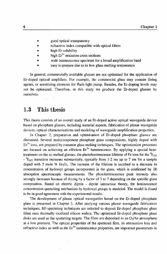
Figure 2.3 shows the PL lifetime as a function of Er3+ concentration in different samples. In Fig. 2.3 (a), the PL lifetime for as-melted PBL samples deercases with increasing Er3
+ concentration. The as-melted P424 samples in Fig. 2.3 (b), show the same effect of PL lifetirne decrease with increasing Er3+ concentratîon, however to a less extent. After heat-treatment, PL Iifetimes for all samples încrease substantially, including PJB glasses (data not shown). For PBL and P424, lifetimes measured with a pumping density of- 0.3 kW/cm2
, are as high as 7 ms fora concentration of 2 mole% Er20 3• As will be explained below, the increase in lifetime after the heat-treatment is due to a decrease of the OH content.

Preparation and optical properties of Er-doped phosphate glasses
11.0 ,-------~---------...,
6.6
~ i 4.4 .J
2.2
0.0 ~----'-----'-----''-----L--0.0 . 1.0 2.0 3.0 4.0
Er Concentratoon {mol.% Er .o;)
(a) PBL glass
11.0
8.8
7il .s 6.6
11! ~
l! 4.4 .J
2.2
0.0 0.0 1.0 2.0 3.0 4.0
Er Concentratoon (mol.% Er P:J
(b) P424 glass
Figure 2.3: Photoluminescence 411312 lifetime as a function of Er concentration. Experimentally measured data are depicted in data points (measuring error within ± 0.2 ms). The drawn lines are based on the Er photoluminescence quenching model proposed in section 2.4.5. The solid lines are for the as-melted samples and the dashed lines fordried samples.
15
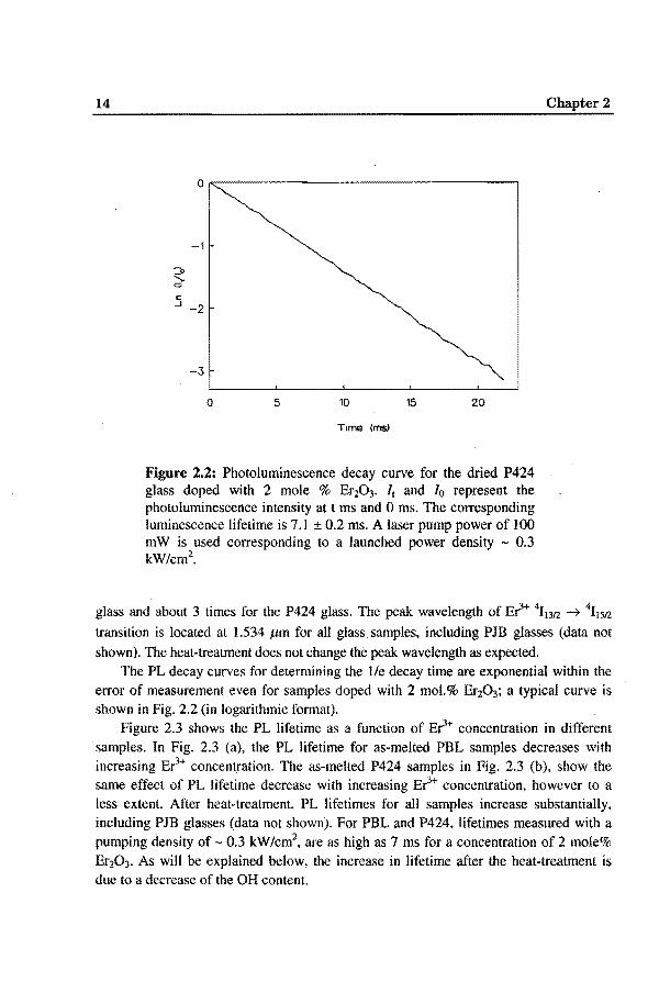
The influence of pump power density on the Er3+ PL lifetime in the P424 glass is
depicted in Fig. 2.4. For thin glass samples, a pump power density as high as 7 kW/cm2
16 Chapter 2
is reached, at which the PL decay curve is still exponential or linear in a logarithmic format within the error of measurement. This dependenee shows that no strong quenching effect occurs up to this pump power density. The PBL and PJB glasses show similar slight lifetime reduction as the P424 glass in Fig. 2.4. It is expected that a cooperative upconversion process occurring at high pump powers and high Er
concentrations, would lead to light emission at 0.98 flm [3]. The fact that the 1.53 flm emission decay time does not change in Fig. 2.4 proves more clearly that there is no upconversion in this pump power range.
10
8
] !!-- ! §: ~
-~ 6
~ 4
~
2
0 0.0 2.0 4.0 6.0 8.0
PL.ITlp power dens1ty (kW/cm")
Figure 2.4: Er photoluminescence lifetime of the dried P424 (2 mol. % Er20 3) glassas a function of pumping density. The line serves as a guide for the eye. The maximum launched pump power density is 7 kW/cm2
•
2.4 Er3+ luminescence quenching by OH
impurities
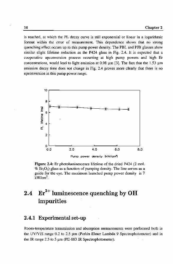
2.4.1 Experimentalset-up
Room-temperature transmission and absorption measurements were performed both in the UVNIS range 0.2 to 2.5 J.l.m (Perkin Elmer Lambda 9 Spectrophotometer) and in
the IR range 2.5 to 5 J.l.m (PE-883 IR Spectrophotometer).

Preparation and optical properties ofEr-doped phosphate glasses 17
2.4.2 Water contentand IR absorption in glasses
The presence of OH groups or water in glass can be characterised by measuring the OH- absorption peaks in the IR-spectrum. In silicate glasses[ 11 ], these absorption peaks
are.located at 2.8 J.lm, 3.6 J.lm and 4.2 J.lm. In phosphate glasses[12], there is a broad
absorption band extended from 2.7 J.lm to 4 J.lm, as will be discussed in 2.4.4 ..
For a given glass sample the total water content can be determined by measuring the absorption coefficients of the OH vibration bands. The linear absorption coefficient
a1 can be calculated from transmission spectra as follows[l3]:
with:
Wh ere:
E a;=-
d
linear absorption coefficient (llcm)
extinction (-) thickness of glass sample (cm) transmission at a specific wavelength outside the absorption region of OH groups
transmission at a wavelength of À. J.lm (-), corresponding to one of the OH absorption maxims
(2.1)
(2.2)
According to the Lambert-Beer law, the extinction is proportional to the concentration c of the absorbing species and the thickness d of the glass sample.
E=excxd (2.3)
The proportional factor e is called the extinction coefficient. The absorption
coefficient is therefore proportional to the water content.
a 1 =cxe (2.4)
The relation between the absorption coefficient a (based on the natura! logarithm),
and the linear absorption coeftïcient CXf, is as follows:

18
a a a=--~-=-~-
log10 e 0.43
Chapter 2
(2.5)
The quantitative detennination of the total OH content in the glass requires a
summation of all three bands and the knowledge of the molar absorption coefficients e for these bands, which demands the availability of independent methods. In genera!, such an independent determination would be necessary for each of the glasses of different composition. In the case of silicate glasses, however, Scholze [14] has shown that the distri bution of the absorbing species among the three IR-bands remains constant when the concentration of OH in the glass changes. Therefore, the detennination of the OH concentration by IR-spectroscopy can be based on a single band. Scholze calculated a practical molar absorption coefficient for the main absorption band by degassing different glasses in vacuum and detennining the released water.
Based on the single band method, the water content can be derived by the following fonnula:
l8000x (0.43·a2 8 ) Cs= .
pxe2.8 (2.6)
With:
Cs con centration of water according to the single band (simplified) methods (wt.ppm)
E2.8 extinction at 2.8 J.Lm (-)
e2.8 extinction coefficient at 2.8~-tm (l cm·• mole.1)
a2.8 absorption coefficient at 2.8 ~-tm (cm·1)
d thickness of the glass sample (cm) p density of the glass sample (g/cm3
)
and:
To (2.7) E= log10 -
T). With
To transmission at a wavelength of 2.5 ~-tm (no OH absorption) Tz.s transmission at a wavelength of 2.8 ~-tm
Preparation and optical properties of Er-doped phosphate glasses 19
Day [15, 16] determined, in the same way as Scho1ze, a practical absorption coefficient for sodium aluminophosphate for the absorption band at 2910 cm-1
, and found a value of 100 1 mole- 1cm-1
• This value is only valid for phosphate glasses with the màin absorplion band at about 3000 cm-1
• According to Arriagada et al [ 17], a value
of e = 90 1 mole-1cm-1 should be used for phosphate glasses where the maximum of the
absorption band occurs at 3350 cm-1•
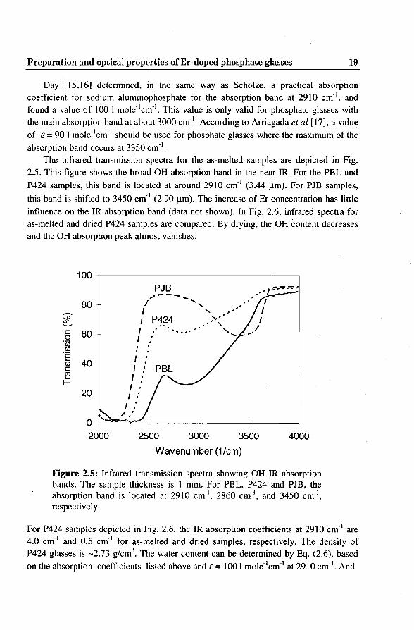
The infrared transmission spectra for the as-melted samples are depicted in Fig. 2.5. This figure shows the broad OH absorption band in the near IR. For the PBL and
P424 samples, this band is located at around 2910 cm-1 (3.44 )lm). For PJB samples,
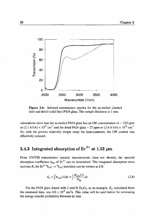
this band is shifted to 3450 cm-1 (2.90 )lm). The increase of Er concentration bas little influence on the IR absorption band (data not shown). In Fig. 2.6, infrared spectra for as-melted and dried P424 samples are compared. By drying, the OH content decreases and the OH absorption peak al most vanishes.
100
PJB . ~-""'="·"""'='"' "-- .......... .... 80 I
' ,
I ' ,
~ I P424 ;-.· ~ -- . "\ c I . . ........... ' 0 60
I -ïii (/) I . .E I . (/) 40 . c I . ~
. I .
I- I . .
20
2000 2500 3000 3500 4000
Wavenumber (1/cm)
Figure 2.5: Infrared transmission spectra showing OH IR absorption bands. The sample thickness is 1 mm. For PBL, P424 and PJB, the absorption band is Iocated at 2910 cm-1
, 2860 cm-1, and 3450 cm-1
,
respectively.
For P424 samples depicted in Fig. 2.6, the IR absorption coefficients at 2910 cm-1 are 4.0 cm-1 and 0.5 cm- 1 for as-melted and dried samples, respectively. The density of P424 glasses is -2.73 g/cm3
• The water content can be determined by Eq. (2.6), based on the absorption coefficients listed above and e= 100 I mole-1cm-1 at 2910 cm-1
• And
20 Chapter 2
100.----------------------------.
80
'ij - .............. 60
40
20
0 ~==~--~------~----~------~ 2000 2500 3000 3500 4000
Wavenumber (1/cm)
Figure 2.6: Infrared transmission spectra for the as-melted (dashed line) and dried (solid line) P424 glass. The sample thickness is 1 mm.
calculations show that the as-melted P424 glass has an OH concentration of- 220 ppm
or (2.1 ± 0.6) x 1019 cm·3 and the dried P424 glass - 27 ppm or (2.6 ± 0.6) x I 0 18 cm·3•
So, with the present relatively simple setup for heal-treatment, the OH content was effectively reduced.
2.4.3 Integrated abs~rption of Er 3+ at 1.53 J.lffi
From UVNIS transmission speetral measurements (data not shown), the speetral
absorption coefficient CXabs of Er3+ can be determined. The integrated absorption cross
sections Ka for Er3+
411312 -,f 411512 transition can be written as [3]:
J Ja b (v)
K = a (v)dv = a s dv a abs IV Er
(2.8)
For the P424 glass doped with 2 mol.% Er20 3, as an example, Ka, calculated from the measured data, was 4.6 x 10·8 cm2/s. This value wil! be used below for estimating the energy transfer probability between Er i ons.

Preparation and optical properties of Er-doped phosphate glasses 21
2.4.4 Glass structures and Er3+ lwninescence properties
The glass host can influence the luminescent properties of rare-earth ions like E~+, which is observed in the PL lifetime of the 4I1312 -
4I1512 transition of excited Er3+ ions. Among other factors, the PL lifetime of Er3+-doped glasses is influenced by the OH content in the glass [18]. IR absorption spectroscopy can provide more information about these OH groups in the glass. It is known [ 19] that the presence and bonding-state of OH groups in glass matrices is closely related to the relative number of non-bridging oxygens in the glass.
Infrared absorption spectra of silicate glasses have been studied extensively [ 11]. The fundamental stretching vibratîons of OH groups experiencing different degrees of
hydrogen bonding give rise to three absorption bands. The band at 2.7 to 2.9 ~m is due
to free OH groups, whereas the bonded or associated OH groups cause peaks to occur
at 3.3 to 3.8 ~mand around 4.2 ~m. Actdition of Ah03 to alkali-silicate glasses brings
about a decrease of non-bridging oxygens, which leads to a decrease of associated OH groups.
In ph~sphate glasses, OH groups can be present at different positions on the phosphate chain, which give rise to different -OH .... O- associations. This difference results in a number of overlapping absorption bands, which combined to give a broad
band. This OH absorption band extends from about 2500 to 3600 cm·' (2.7 to 4 ~m), due to the fundamental stretching vibration of OH groups, as in silicate glasses [ 12].
In Fig. 2.5, the PBL glass rich in alkali and alkaline earth ions, having a relative high number of non-bridging oxygens, mainly show associated OH groups which have a peak around 2800 cm·l. P424 and PJB glasses both have a high Ah03 content, leading to a much lower concentration of non-bridging oxygens and thus most of the OH groups in these as-melted glasses are expected to be present in a free bonding state, similar to the case of aluminosilicate glasses. An OH absorption band is indeed observed for the PJB glass at around 3500 cm-1
• It is interesting to note that the absorption band for asmelted P424 glass having a similar amount of Ah03 as in the PJB glass is located at a different position and has a different band shape, although the intensities of the two peaks are almost similar. The OH absorption band of the P424 glass is rather similar to the band of the PBL glass and is located at almost the same position, only ha ving a much lower intensity. We suggest that these observations show that the P424 and PJB glass have different glass structures in spite of similar Al20 3 contents.
The complex role of Ah03 in phosphate glasses has been discussed recently [20]. lt is shown that for sodium aluminophosphate glasses there is a structure change at the pyrophosphate stoichiometry (overall 0/P ratio = 3.5), and it is also suggested that a second change occurs at the orthophosphate stoichiometry (0/P=4). In Table 2.2, the structural characteristics of our phosphate glasses are listed. As shown in Table 2.2,

22 Chapter 2
0/P is 3.75 tor P424 glasses and 4.34 for PJB glasses. The observation that phosphate glasses having different values of 0/P give different OH infrared absorption bands, supports the above mentioned predictions.
Linking the IR absorption spectra for the as-melted glasses to the measured values of the 411312 PL lifetime of Er3+ ions, the following observations can be made. The P424 and PJB glass incorporate OH groups with different bonding states but have similar OH absorption peak intensities. The PL lifetimes for both glasses are similar. On the other hand, the P424 and PBL glass having really different OH absorption peak intensities, give different PL lifetimes. The lower the infrared absorption peak, the higher the lifetime of Er i ons. The general condusion is that Er3
+ PL lifetime is influenced mainly by the amount of OH content in the glass, rather than by the specific OH bonding state.
Table 2.2 Structural Characteristics of studied Phosphate Glasses
Alz03 Nonbridging OH bonding
Glass Content (mol%) 0/P molar ratio oxygens state
PBL -3 3.07 rich associated
P424 -20 3.75 less associated
PJB -20 4.34 less free
2.4.5 Modeling ofEr3+ luminescence quenching by hydroxyl groups
It has been suggested by several authors that OH groups are serious queuehers of the photoluminescence of Er ions in phosphate glasses [9,18]. In a luminescence study on Er-doped alkali-silicate glasses [10], a similar condusion is reached that Er3+ PL lifetime reduction has a combined rather than a separate dependenee on both the Er3
+
and OH concentrations. A possible two pbonon queuehing mechanism by OH groups is suggested [10]. Based on this suggestion, a simplified energy transfer and queuehing model is described here to explain the observed Er3
+ luminescence queuehing quantitatively.
A general theory of concentration queuehing bas been proposed years ago by Förster and Dexter [21]. According to this theory, the energy transfer probability per unit time between two nearby Er3
+ ions by the electric dipole - dipole interaction is equal to:

Preparation and optica! properties of Er-doped phosphate glasses
where:
n = refractive index c = velocity of light in vacuum h = Planck's constant 'l'o = Er3+ PL lifetime without energy transfer R the separation of the two neighboring Er3+ i ons
and
23
(2.9)
Q. is the integrated absorption cross section of the Er3+ ions, Q.=fa(E)dE = hK., Ka is
from Eq. (2.8)./a(E) and fe(E) are normalized shape functions of the absorption and
emission spectra, and /t(E)dE=l. R0 is a critica! distance at which Pdd equals ll'l'o. Let
N0 = ( 4n:R03/3r1
, N0 is a critical concentration.
With the following input data for Eq. (2.9), we can estimate the values of R0 and N0•
E = 0.81 eV for the 4l1312-
4/ 1512 transition
n 1.50 (measured by Abbe refractometer)
Q. = hKa = 1.9 x 10⁻²² cm2eV (see Eq. (2.8))
'lb = 10.5 ms (measured lifetime fora P424 glass doped with 0.02 mol.% Er20 3 )
/fa(E)fe(E)dE"" 1 (eVr1 (assuming a maximum overlap betweenfa(E) andfe(E))
One gets R0 12.1 Á, and N0 = 1.35 x 1020 cm-3• Th is means that when the Er
concentration is equal to 1.35 x 1020 cm-3, the Er- Er interaction is strong enough that
the energy transfer probility is equal totheEr radiative decay probibility. The Förster-Dexter theory [21] deals with the microscopie case of two ions
interacting with one another. Concerning the macroscopie case with many ions, the energy transfer process in a glassy matrix can be treated as an energy diffusion process
[22]. The concentration dependent lifetime rcan be written as:
(2.10)
where 'lb is the lifetime without experiencing energy transfer as in Eq. (2.9). I/r0 is quenching rate due to energy transfer by electrical dipole - dipole interactions, and is
24 Chapter 2
dependent on both the Er3+ and OH concentrations. The exact form of r0 will be
described below. Three assumptions are proposed to build the present Er concentration quenching
model. (i) The OH quenching centers are only coupled efficiently to a fraction of Er ions. (ii) The amount of Er3
+ ions coupled to OH groups is dependent on the OH
concentration in the glass, NEr-OH = f3 NoH (iii) Non-radiative quenching occurs after the
excited energy is transferred to Er ions coupled to OH groups, possibly via a two pbonon mechanism. Thus, with an increasing Er concentration [above the critical concentratien predicted by Eq. (2.9)), energy transfer between excited Er ions and ground state Er ions increasingly takes place. The excited energy will be lost whenever it is transferred to an Er3
+ ion coupled to an OH quenching center. Taking into account these assumptions, the activators (Er ions) and queuehers (Er
ions coupled to OH groups) are essentially identical as far as energy transfer is
concerned, and one has a simplified formula for lltb in Eq. (2.1 0) [22],
(2.11)
with k = 8nRQ6/'to or k = (9/2n)('rr/Vo2r1, and NEr-OH = f3 NoH· r0, Ro and No are defined in
Eq. (2.9).
Combining Eq. (2.10) and Eq. (2.11), we get 1/r as a function of NEr·
1 1 - = -+ 81CCEr ErNoHNEr r r0 •
(2.12)
where CEr.Er = (R/Iro ){3.
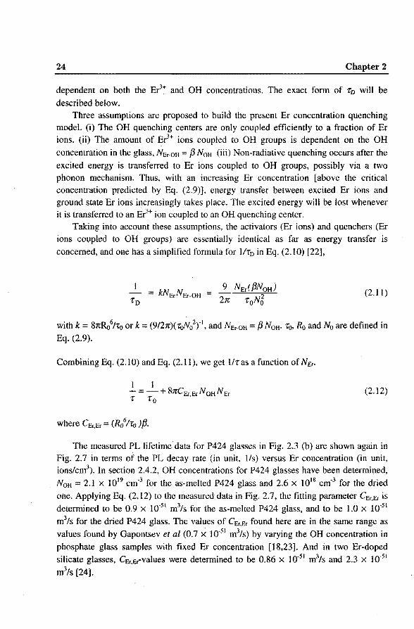
The measured PL lifetime data for P424 glasses in Fig. 2.3 (b) are shown again in Fig. 2.7 in terms of the PL decay rate (in unit, 1/s) versus Er concentration (in unit, ions/cm\ In section 2.4.2, OH concentrations for P424 glasses have been determined,
NoH 2.1 x 1019 cm'3 for the as-melted P424 glass and 2.6 x 1018 cm·3 for the dried
one. Applying Eq. (2.12) to the measured data in Fig. 2.7, the fitting parameter CEr,Er is
determined to be 0.9 x 10'51 m3/s for the as-melted P424 glass, and to be 1.0 x 10'51
m3/s for the dried P424 glass. The values of CEr,Er found here are in the samerange as
values found by Gapontsev et al (0.1 x 10'51 m3/s) by varying the OH concentration in
phosphate glass samples with fixed Er concentration [18,23]. And in two Er-doped
silicate glasses, CEr.Er-values were determined to be 0.86 x 10'51 m3/s and 2.3 x 10'51
m3/s [24].

Preparation and optica! properties ofEr-doped phosphate glasses
800 ,------------------------------,
700
-600 .se ,... -; 500 10 ~ 400 ro 0 ()) 300 -o
...J a.. 200
100
0 0
0 •• - •.•• 0 •• 0 ••••
2 4 6
..... ?!i~9- --. ---
8 10 12
Er concentration {x 1 o20cm·3) 14
Figure 2.7: The dependenee of the Er PL decay rateon the Er concentration for as-melted and dried P424 glasses having different OH group concentrations. The data points are experimentally measured data from Figure 2.3 (b) and the drawn lines are the fitting lines explained in the text.
25
The Er PL lifetimes for P424 glass, predicted by Eq. (2.12) with the CEr,Er
determined above, are shown in Fig. 2.3 (b ). It can be seen that the predicted lifetime for the dried glass deviates from the measured data. The predieted value lies below the measured data at a low Er coneentration and above the measured data at a high Er concentration. Apparently, the energy transfer between Er ionsis Iess severe fora Iow Er concentration, which leads to less quenching. We suggest that the lower PL lifetime than predicted at a high Er concentration is due to additional queuehers other than OH groups becoming effective in quenching E~ luminescence for the dried glass.
For PBL glass, similar curves are drawn in Fig. 2.3 (a). As ean be seen from Fig. 2.3 (a), the model prediets correct lifetime reduction trends for as-melted PBL glasses. Again the predicted values for the dried samples deviate somewhat from the measured data, due to the same reasons as explained for the P424 glass.
2.5 Conclusions
Er3+ 1.5 J.lm luminescenee queuehing in phosphate glasses at high Er concentrations is
examined. For as-melted phosphate glasses, the Er3+ PL lifetime decreases rapidly upon

26 Chapter 2
increasing the Er3+ doping level. This decrease is attributed to a combined
concentration quenching process depending on both the Er3+ dopant concentration and
the OH concentration in the glass. A concentration quenching model by OH groups is proposed and it agrees well with the measured Er PL lifetimes.
The controlled heat-treatment deercases the OH concentration and results in an increase of the Er3
+ PL lifetime for different Er concentrations. PL intensities also increase along with the increase of the lifetime. The heat-treatment is effective for all three types of glasses although there is a pronounced difference in the glass structure.
References
[1] E. Snitzer, Phys. Rev. Lett 7, 444 (1961)
[2] M. J. Weber, "Science and technology of laser and glass", J. Non-Cryst Solicts 123, 208 ( 1990)
[3] W. J. Miniscalo, "Erbium-doped glasses for fiber amplifiers at 1500 nm", J. lightwave technoL 9, 234 (1991)
[4] C. H. Henry, G. E. Blonderand R. F. Kazarinov, J. Lightwave Techno!. 7, 1530 (1989)
[5] H. Yajima, S. Kawase and Y. Sekimoto,"Amplification at 1.06 J.lm using a Nd:glass thin-film waveguide", Appl. Phys. Lett. 21,407 (1972)
[6] W. J. Miniscalo, L J. Andrews, B. A. Thompson, T. Wei and B. T. Hall, "The effect of glass composition on the performance of Er3+ fiber amplifiers", SPIE vol.117l Fiber Laser Souree and Amplifiers, 93-l 02 ( 1989)
[7] J. Wang. W. S. Brocklesby, J. R. Lincoln, J. E. Townsend and D. N. Payne, "Local structures of rare-earth ions in glasses: the 'crystal-chemistry ' approach", J. Non-Cryst. Solids 163,261 (1993)
[8] T. Nishi, K Nakagawa, Y. Ohishi et al, "The amplification properties of a highly Er3
+ doped phosphate fiber", Jpn. J. Appl. Phys. 2, Lett. 31 (2B), Ll17-9 (1992)
[9] N. E. Alekseev, V. P. Gapontsev, A. K. Gromov, S. A. Zelentsova,A. Aizyneev, V. B. Kravchenko, N. A. Pararoenova and Y. P. Rudnitskii, "Influence of hydroxyl groups on the luminescence properties of phosphate glasses activated by rare earth ions", Izv. Akad. Nauk SSSR, Neorg. Mater., 11 (2), 323 (1975) (Engl. TransL in Inorg. Mater. 11 (1975) 270)
[10] A. J. Bruce, W. A. Reed, A.E. Neeves, LR. Copeland, W. H. Grodkiewicz and A. Lidgardet, Mat. Res. Soc. Symp. Proc. 244, 157 (1992)
[11] H. Scholze, "Oases and water in glass, part one", Glass Industry 47,546 (1966)
[12] G. A.C. M. Spierings, "The near infrared spectra of water in phosphate glasses", Glastechn. Ber. 56K, Bd.2, 1130 ( 1983)
( 13] C. R. Bamford, "Colour generation and control in glass", (Published by Elsevier North-Holland Inc., New York), p. 13, 1977

Preparation and optical properties ofEr-doped phosphate glasses 27
[14] H. Scholze, Glastechn. 32 (1959) 81, 142,278,381,421
[15] D. E. Day and J. M. Stevels, "Effect of dissolved water on the internat friction of glass", J. Non-Crystalline Solids 14, 165 (1974)
[16] D. E. Day, "Intemal friction of glasses with low water contents", J. Am. Ceram. Soc.57,530(1974)
[17] J.C. Arriagada, W. Burkhardt and A. Feltz, "The influence of the water content on absorption and dispersion behaviour of calcium metaphospahte glasses", J. Non-Crystalline Solid. 91, 375 (1987)
[18] V. P. Gapontsev, S. M. Matitsin, A. A. lsineev and V. B. Kravchenko, "Er glass lasers and their applications", Opties and Laser Technology 14, 189 (1982)
[ 19] R. V. Adams, "Infra-red absorption due to water in glasses", Phys. Chem. Glass 2, 39 (1961)
[20] R. K. Brow, "Nature of alumina in phosphate glass: 11, structure of sodium aluminophosphate glass", J. Am. Ceram. Soc. 76, 919 (1993)
[21] D. L. Dexter and J. H. Schulman, ''Theory of concentradon quenching in inorganic phosphors", J. Chem. Phys. 22, 1063 (1954)
[22] F. Auzel, "Multiphonon processes, cross-relaxation and up-conversion in ionactivated solids, exemplified by minilaser materials", in Radiationless Processes (B.Di Bartolo, ed.), PlenumPress, p. 213, 1979
[23] V. P. Gapontsev, A. A. Izyn~v. Yu. E. Sverchov and M. R. Syrtlanov, "Mechanism and parameters of the quenching of luminescence of rare-earth ions by hydroxyl impurity groups in laser phosphate glass", Sov. J. Quanturn Electron. 11, 1101 (1980)
[24] E. Snoeks, P. G. Kik and A. Polman, ''Concentration quenching in erbium implanted sodalime silicate glass optica! waveguides", Opt. Mat. 5, 159 (1996)

Chapter 3
Development of phosphate glass planar waveguide by RF sputtering
3.1 Introduetion
3.1.1 Choice of deposition techniques ofphosphate glass waveguides
Many review articles on fabrication of thin film waveguides for integrated opties have been publisbed [ 1,2,3]. As for glass optical waveguides, there are several available fabrication processes, including sputtering, ion-exchange, ion-implantation, flame hydrolysis and spin coating or sol-gel methods [4]. Among these methods, the most popular one is ion-exchange.
Since 1980s, much workon ion-exchange has been conducted [5]. The advantage of this metbod is that low cost and low attenuation loss waveguiding components can be produced on glass substrates. Rare-earth doping can be realized during fabrication of the glass. Until now, some good results have been achieved with ion-exchange techniques [6,7]. However, ion-exchange processes can be applied only to glass or crystal substrates containing mobile i ons and precise control of ion-exchange process is difficult.
Flame hydrolysis processes work well with silica-based glasses, for instanee silica codoped with P/Al. Er-doped waveguides show a background loss of 0.2 dB/cm [8]. However, it is difficult to apply this metbod to multicomponent glasses, like phosphate glass systems.
The sol-gel metbod is a versatile technique. It is specially attractive for integration of rare-earth-doped devices with other integrated optica! devices on the same substrate. The film composition can be varied in a relatively wide range. lt allows easy incorporation of Er ions just by adding an Er compound into the starting solutions. Low-loss borophosphosilicate glass films have been achieved by sol-gel deposition [9].
30 Chapter 3
However, it is difficult to remove all OH groups in the film. As discussed in chapter 2, OH-groups are serious queuehers for Er luminescence. Besides, drying and densification processes have to be studied wel! in order to prevent cracking of the films.
Furthermore, fabrication of optica! waveguides in crystalline substrates by helium ion-implantation for modification of the refractive index, was reported (IO]. The observed waveguide loss was in the order of 1 dB/cm. To our knowledge, no reports are available on fabricating optica! waveguides on glass substrates by helium ionimplantation. However, ion-implantation has been employed successfully to implant rare-earth ions into undoped silicate glass layers [11] and Ah03 films[l2].
As for radio-frequency (RF) sputtering techniques, high quality multicomponent glass waveguides have been produced in the past [13,14,15,16]. The processitself is compatible with standard IC technology. When silicon substrates are used, inlegration with other devices can be achieved easily. Therefore, in this study RF-sputtering methods have been chosen to fabricate Er-doped phosphate glass waveguides.
3.1.2 RF-sputtering techniques
Sputtering is a widely used method for deposition of thin film optica! waveguides. Thin film formation results from the acthesion of atoms to a substrate. The atoms are ejected from a target by bombardment of ions, which are created, for example, in a glow discharge plasma or by an ion beam. The principles of various sputter deposition methods are covered in several review articles and textbooks [17,18,19,20]. Only a brief introduetion is given here with emphasis on the sputtering of glass films.
The most simple sputter system, known as planar diode sputtering, consists of a target holder as the cathode and a substrate platform as the anode. When a negative potential is applied to the cathode, a glow discharge (plasma) ignites within the vacuum chamber when the appropriate pressure is maintained. The plasma usually consists of argon gas ions. The target is bombarded by ions which physically chip atoms off the target, causing them to be ejected from the surface and subsequently strike the substrate and adhere. In this manoer a high quality film is gradually built up. The sputtered films are usually more dense than evaporated films [ 17].
While a metal target can be readily sputtered by applying a DC current, an insulating target can only be sputtered by applying a Radio-Frequency (RF) poten ti al to the cathode, known as RF sputtering. Otherwise the insulating target will be charged up positively until it repels any further positive ion bombardment RF-sputtering can also be applied to metal targets. The deposition rate of dielectric films is normally much Jower than that of metal films.
In practice, the sputtering rate can be increased by applying a magnetic field normal to the target surface, known as magnetron sputtering. When a magnetic field is coupled
Development of phosphate glass planar waveguide by RF sputtering 31
with sputtering sources, the magnetic field traps electrous close to the target surface, and hence deercases the mean free path of electrous in the discharge. More ions are created by electron impact close to the target and this leads to an increase of the sputtering rate.
A wide variety of oxide optica! films have been deposited by RF sputtering, such as Si02 [21], Alz03 [22] and ZnO [23]. The optica! loss of these films was- 1 dB/cm. Commercially available muitkomponent glasses, in most cases silicate glasses, have been used as glass targets to prepare thin glass films, for instanee Pyrex 7740 [24], Corning 1720 [25] and Corning 7059 [26]. Frequently, RF-sputtered films of menoxides or glasses are found to have a dissimilar chemica! composition and to have different refractive indices as the target materials. The increased absorption loss and different refractive index compared to the target materials are the results of a) oxygen loss caused by dissociation of the elemental oxides during sputtering [2), and b) preferential sputtering of different elements in the target. In some cases, the resulting high optica! loss could be decreased by post annealing, or by changing sputtering parameters.
The first RE-doped glass waveguide was produced in 1972 by sputtering a Nddoped barium crown glass on a Corning 7059 glass substrate [13]. The thin glass film
was spottered in an Ar atmosphere with a substrate healing of 300°C. It was mentioned that heating of the substrate was important to rnaintaio the growth of a glass film with
good optica! quality. A low optica! toss of 0.45 dB/cm at 1.06 J.Lm was achieved. In
another report [14], Nd-doped American Optica! barium crown glass 1838 and 0835 were used as targets. The glass film was deposited in an oxygen atmosphere with a pressure of 0.66 Pa. The film was reported to be slightly brown and to have a high opticalloss right after deposition. High-quality films were obtained only after annealing
in air at 500°C for more than 15 hours, resulting in a low optica! loss of 0.15 dB/cm at
1.06 J..llli. Studies on sputtering Er-doped silicate glasses on silicon substrates have shown
good results. The waveguide loss is - I dB/cm [ 15]. The level of Er doping in the film was easily varied by changing the Er doping in the target glass. High Er lifetime of 5 to 9 ms was preserved by post annealing in pure oxygen. Recently, the quality of the waveguide was further improved by adopting a re-flow technique, resulting in a
background loss of 0.24 dB/cm at 1.3 J.Lm [27].
Sputtering of phosphate glasses has hardly been studied. The only relevant report on this subject is a study on sputtering a Nd-doped phosphate glass (Schott LG -760) to fabricate a waveguide laser on a silicon substrate [ 16]. High quality glass films were obtained by magnetron sputtering with a large target-substrate-distance of 12 cm. The
attenuation loss at 632.8 nm was 2 dB/cm. Lasing at 1.06 J..Lm was observed using a dye
pump laser, operating at 803 nm.
32 Chapter 3
3.1.3 Attenuation ofthin sputtered optical waveguides
Most glasses are excellent optical materials, transparent in the visible and near infrared range. Thin glass films fabricated by ion-beam based sputter processes, however, have a background toss of 0.5 dB/cm to > 2 dB/cm, at least lO times higher than that of bulk glasses [2]. Although very low loss sputtered films have been obtained, the typicalloss of sputtered film at 632.8 nm is - I dB/cm [28].
In general, the optica! loss mechanisms of thin glass films can be divided into two categories, namely material related loss and waveguide geometry indoeed loss mechanisms. Material related attenuation refers to absorption loss and scattering toss in the film. This attenuation can be caused by changes in the stoichiometry of the original constituents, by the introduetion of impurities and by local changes in the glass structure, e.g. resulting in variations in refractive index. Geometry induced attenuation includes surface scattering due to surface roughness and rough side-walls in case of channel waveguide, and loss-inducing effects from the surrounding medium. For spottered glass waveguides, it is believed that film absorption and scattering Ioss, and surface scattering loss are the main sourees of the total attenuation loss [29].
In a study on spottered silicate glass films [28], the surface scattering loss due to the surface roughness was evaluated by using an expression based on the Rayleigh criterion [30]. The results showed that for an average surface roughness of lO Á, the
surface scattering Joss was about O.ldB/cm when the film had a thickness of 1 J.lm or more [28]. The effect from the surrounding media can be decreased by choosing a low loss substrate or a buffer layer of high quality and proper thickness. It is known that RFsputtered films can be oxygen deficient [2]. In general, this will lead to an increase of the film refractive index and the opticalloss. Annealing in air at elevated temperature can restore the oxygen content deficiency and deercase the opticalloss.
In practice, it is often difficult to identify the real loss mechanisms. Therefore it is also difficult to find the proper solutions to deercase the optica) loss. Consequently, achieving a high quality optica! thin film is usually a tough and time consuming process.
3.1.4 Requirements ofthe Er-doped films for optical amplifier applications
It is useful to reeall some requirements for ideal waveguide materials [2], which form the major objectives of the development of Er-doped phosphate glass film waveguides:

Development of phosphate glass planar waveguide by RF spnttering
• Low absorption loss at the excitation wavelength.
• Minimum scattering defects to achieve a totalloss (absorption plus
scattering ) of maximum l dB/cm or less.
• Good refractive index selectivity with a precision upto 0.0001.
• Can be processed into proper waveguide dimensions.
33
Besides the above general requirements for optica! waveguides, efficient Er luminescence properties have to be maintained for applications of active optica!
waveguides; typically, the Er luminescence lifetime at 1.53 lliD should be minimally
around 4 ms. In Chapter 5, a model on the optica! gain of the Er-doped planar
waveguide is presented and the influence of the Er lifetime at 1.53 !liD on the optica!
gain is discussed. It is a complicated process to develop a thin film process. There are many
parameters to be monitored and studied, related to compositional, structural, mechanica! and thermal properties of the deposited films. In view of the final application in this study, the most importance properties are the attenuation loss of the
film and the Er luminescence properties of the transition at 1.53 11m. Therefore, the
optimization process in this study was directly focused on these two parameters. In the experiments, standard silicon wafers (3-inch in diameter) were used as
substrates. The silicon substrates were thermally oxidized to provide a buffer layer for the Er:glass guiding layer. The Si02 buffer layer should be thick enough to prevent the leakage of light into the silicon substrate. The required thickness of the Si02 buffer layer is dependent on the confinement of waveguide modes in the guiding layer, which are characterized by film thickness, refractive index and applied wavelength. In Chapter 4, the theory on waveguide modes is presented and a computer program is introduced [31], which is based on the integrated opties theory.
Calculations were conducted based on the computer model [31] to estimate the required thickness and refractive index of the guiding layer, and the thickness of Si02
buffer layer. The results show that light could be confined in a 2 J.lffi thick Iayer with a
refractive index of 1.50 at a wavelengthof 1.53 11m; the Si02 buffer layer (n 1.44 at
I .53 !liD) has to be 3 11m thick so that the light leakage to the silicon substrate is
negligible. The refractive index of the deposited film and thickness were measured by a prism
coupling set-up. In some cases, the composition of the sputtered films was measured. No attempt was made to control the film structure. The thermal properties and stress of deposited films are important and have their effects on the optica! and luminescence properties of deposited films. They were studied by monitoring film Ioss and Er luminescence.

34 Chapter 3
3.2 Sputtering system
An Alcatel SCM-450 RF-sputtering equipment is used, which is a planar diode system. The vacuum is maintained by a turbomolecular pump, which provides a base pressure of- 3 x 10·7 mbar. The standard target is 4 inch in diameter. The target is positioned
below the substrate with a sputter-up arrangement, see Fig. 3.1. The target is cooled by attaching it to a water-cooled copper backing-plate. The target-to-substrate distance can be adjusted easily from 5 cm to 10 cm by a handle outside the vacuum chamber. The substrate holder can be grounded or unearthed during sputtering. Argon and oxygen are introduced into the vacuum chamber through a needie valve and measured by a MKS flow meter. The pressure in the vacuum chamber can be adjusted by a throttle, from -0.3 Pa to - 5 Pa. The matching network can be tuned automatically to have a maximum forward power.
Vacuum Chamber
SUbstrata
Sputter Gas -+ --~) Vacuum
TFd ~--···
RF Power
Figure 3.1: Schematic illustration of a planar RF-diode sputtering system. The substrate was positioned above the target.
The system can operate in either a sputtering mode or an etching mode. Under etching mode, the substrate can be cleaned inside the chamber to remove any residual impurities on the surface. A cylindrical magnet can be positioned under the copper backing plate. Without the magnet, the system operates in a RF diode sputtering mode. When the magnet is present, the system operates in a RF magnetron sputtering mode.
3.3 Conventional RF diode sputtering of phosphate glass films
Development ofphosphate glass planar waveguide by RF sputtering 35
3.3.1 Introduetion
The RF diode sputtering contiguration is used in the preliminary study. Afterwards, the RF-magnetron sputtering technique is adopted to prepare the Er"doped phosphate glass films. However, the knowledge gained with the RF diode sputtering is still relevant to the experiments followed.
This section is focusing on the characterization of film compositions. Optimization of both the sputtèring process and the target composition is presented.
3.3.2 Experimental
Preparation of glass targets forsputtering
Glass batches were prepared by mixing pure Na2C03, Ah03 and Er20 3 with orthophosphoric acid in an alumina crucible. The mixture was dried at low temperature for a sufficient time to remove most of the water inside the batch. The dehydrated batch was melted at I 000°C to 1400°C, depending on batch composition. The melt was kept
for - 6 hours at the melting temperature, and then poured into a cylindrical graphite mold I 0 cm in diameter.
The resulting glass has a high thermal expansion coefficient and special care was taken to choose the right annealing process. The glass disk was allowed to stand at the annealing temperature for a few hours, foliowed by cooling at a low cooling rate of
0.5°C/min. An Er-doped phosphate glass target forsputtering was obtained by polishing
the glass disk to 6 mm thickness. The compositions of the three glass disks prepared are listed in Table 3.1. The
target NAP I has a composition of the P424 glass discussed in Chapter 2 and RFsputtering experiments start with this target. The other two targets are used later on as discussed in the following text.
Sputtering process
Er-doped thin films were deposited firstly by planar diode RF sputtering. The Er-doped phosphate glass disks were used as target. The target was mounted on a water-cooled copper backing plate. The RF power was varied between 50 W to 600 W. A power of 250 W was found to be safe for the target arrangement. At higher power, cracking of
the target took place. Standard 3 inch silicon wafers with an oxidized layer of 3 f.!m were used as substrates. The substrate was cooled by the water-cooled metal holder. The distance between the substrate and the target was kept at 50 mm. Before deposition, the substrate was cleaned by back-sputtering with Ar in the chamber.

36 Chapter 3
Working pressures, varying between 0.75 Pa and 2.5 Pa were used. Pure Ar and Ar/02 mixed gases were used in the experiment as process gases. Both composition and pressure of the working gas were found to influence the film composition and the deposition rate.
Postannealing
The as-deposited films were annealed in pure 0 2 (99.995 vol.%) in a tube furnace. The
annealing temperature was varied from 300 to 500°C. The annealing time was kept at 1
hour.
3.3.3 Results and discussions
Film thickness and sputtering rate
The film thickness varied from the center to the edge typically by a factor of 2. The
typical film thickness was I ~m at the center. The sputtering rate was dependent on the
sputtering parameters and the target used. For target NAP lil (see table 3.1), the highest
sputter rate at the center was - 0.36 ~m per hour when sputtering in pure Ar at-0.75 Pa.
The influence of the oxygen partial pressure on the sputtering rate is shown in Fig. 3.2.
-;:::I 0 ~ 0.32 e 0 g o.24 Q)
'ê 0.16 0'1 c:
·;::: Q) =s 0.08 a.
(/)
0 20 40 60 80
02 ratio(%)
Figure 3.2: Sputtering rate versus 0 2 ratio in the gas mixture. The working pressure was around 0.75 Pa. RF power was 250 W. The data are for target NAP liL

Development of phosphate glass planar waveguide by RF sputtering 37
In sputtering of oxide glasses, oxygen is normally needed in the sputtering gas to prevent the deficiency of oxygen in the deposited films [2]. With oxygen in the sputtering gas, energy must first be expanded to break down the 0 2 molecule; then the atoms have to b~ positively ionized by stripping an electron from an atom having a high electron affinity. Thus, less energy is available to the positive ions for impacting the target as compared to the case with an inert gas like argon [18].
It is shown in Fig. 3.2 that the sputtering rate decreases when the oxygen partial pressure increases, given a constant total gas pressure. The sputtering rate with 20%0z/80%Ar is about half of that with pure Ar. With an increase of 0 2 ratio from 20 % to 84 %, the sputtering rate decrease about 3 times.
When the 0 2/ Ar ratio was kept constant, the total gas pressure had a small influence on the sputtering rate. The sputtering rate slightly increased with a higher pressure.
Characterization of film compositions
The deposited films were characterized by Energy Dispersive Analysis of X-ray (EDAX) and by X-ray Photoelectron Spectroscopy (XPS) analysis. Both analysis methods indicate the presence of P, Al, Na and Er in the film. EDAX analysis does not provide an accurate determination of the film composition. With XPS measurements, accurate film compositions (accuracy about 1 at.%) and compositional depth profiles were obtained.
The XPS measurements showed that glass films deposited in pure Ar were deficient in P content to a great extent and had a significant surplus of Al camparing to the target composition. The P content of the film could be increased when sputtering in Ar/02
gas, but the Al content was still about 2-3 times higher than that in the target. The Na content in the film was 2.5 times lower than that in the target. A typical film composition (D3), tagether with the original target composition (NAP 1), is shown in Table 3.1. The results suggest that Al has a high preferenrial sputtering rate compared to P and Na, leading to a large deviation of film composition from target composition. Film compositions stoichiometrically identical to the target glass could not be obtained by further increasing 0 2 partial pressure in the chamber or by varying other process parameters.
In literature studies on sputtering borosilicate glasses [28], a similar deviation of the film composition from the target glass was observed. Volatile elements like boron and barium were found to be def'icient in the film. In another study [32], significant loss of P was identified during sputtering calcium phosphate glass in argon.
There are many factors which cause a deviation of film composition from the target composition [33]. For instance, sublimation of volatile elements may occur at substrate and target surfaces due to heating effects by bombardment of energetic ions and

38 Chapter 3
neutrals, if the substrate and target are not well cooled. The dissociation of weakly bonded P20 5 might also be the cause of P loss during sputtering [33].
Table 3.1 Compositions of targets and films sputtered with 25%02n5%Ar, 2.5 Pa
Composition (at.%) p AI Na Er 0
Target NAP I 15.9 7.9 15.0 0.80 60.4
Film D3 9.5 19.9 6.0 0.72 61.4
Target NAP 11 18.9 3.9 15.4 0.39 61.4
Film D6 14.2 12.7 10.4 0.38 61.9
Target NAP lil 22.3 3.3 7.9 0.68 65.8
Film D9 18.1 8.9 5.4 0.73 66.8
20~--------------------------------.
~ §.15. c: 0
:;::;
~ ~ 10 (.) c: 0 u (.)
.E 5
~
0 20 40 60
Sputtering Time (in minutes)
p Al Na
80
Figure 3.3: The compositional depth profile of the film 06 versus sputtering time measured by XPS. Only profiles of the main elements P, Al, Na and Er are shown. Er concentration is enlarged by a factor of 5 in the figure. The variation of the measured data at the outer surface is due to the C contamination in the ambient enviroment.

Development of phosphate glass planar waveguide by RF sputtering 39
In order to get a film composition close to the original target composition, the P content in the target has to be increased and the AI content has to be decreased. A modified target composition (NAP 11) and the resulting film composition (D6) are shown in Table .3.1. Both the P and Na contents increase along with the decrease of Al content in film D6 camparing to film D3. This result shows that a desired film composition can be reached by choosing suitable target composition, despite of preferential sputtering for different elements in the glasses. Another modified target NAP III and the resulting film D9 are also shown in Table 3.1.
The XPS measurements also provided compositional profiles of deposited films. Fig. 3.3 shows the concentration depth profiles of the main elements in film D6. Besides the C contamination on the outer surface, the films have uniform P, Al, Na and Er concentrations throughout the thickness of the film.
lnfluence of sputtering gas mixture and gas pressure on deposited films
During the XPS measurements, the valenee state of P was monitored. In Fig. 3.4 (a), a part of the XPS spectrum is shown in the range of a binding energy of 120 e V to 145 eV, for one film deposited with a gas mixture of 25%02n5%Ar at a low pressure of 0.75 Pa. A side peak is visible around the P2p peak in the XPS spectrum. This side peak is ascrîbed to P in the atomie form. It is thus concluded that under eertaio conditions, a part of the P20 5 might be reduced during the sputtering process, which is an unwanted effect.
8
~ 6
w z 4
2
10.-----------------~
(b) 8
~ 6
w z 4
140 135 130 125 120
Binding Energy (eV) 140 135 130 125 120
Binding Energy (eV)
Figure 3.4: XPS spectra of P2p absorption peak Iocated around 133 eV. A side peak is visible in (a) with 25%02175%Ar, 0.75 Pa and no side peak in (b) with 50%02/50%Ar, 0.75 Pa

40 Chapter 3
When films were sputtered at the same pressure, but with a gas mixture of 50%0i50%Ar, XPS measurements showed that the side peak of the P2p peak disappeared in the XPS spectrum, as shown in Fig. 3.4 (b). When the 0 2 ratio in the gas mixture was kept at 25% and the gas pressure was raised above 1.2 Pa, the deposited film also contained only P20 5• So in order to ensure that all P is present in the P20 5
form in the sputtered films, the 0 2 partial pressure in the sputtering chamber should be sufficient (> -0.3 Pa). This can be realized by a proper combination of the Ar/02 ratio and the gas pressure.
3.3.4 W aveguide properties of RF diode sputtered
phosphate glass films
Er3+ Photoluminescence spectroscopy was performed with the RF diode sputtered Er
doped films. The films showed Er luminescence spectra around 1.53 J.tm. It was found that annealing in pure oxygen could effectively improve the Er luminescence yield. Detailed discussions on the Er luminescence properties of sputter-deposited Er-doped phosphate glass films wiJl be presented in the following sections.
However, it appeared that the deposited films had very high attenuation losses, since no guiding He-Ne laser light at 632.8 nm was observed. lt can be assumed that the waveguide loss of the films is well above 100 dB/cm. In order to be used as guiding media, the film background loss should be maximum 1-2 dB/cm at the signal wavelength, preferably below 1 dB/cm. The cause of the high loss might be the sputtering process itself. Sputtering parameters may not yet be optimized with respect to the film loss. The sputtering power is kept at 250 W to prevent over-heating of the target. Other parameters are adjustable, such as gas mixture, working pressure, substrate temperature and target-to-substrate distance.
The optimization process. was explored briefly in order to deercase the film loss. No low loss films were obtained by varying sputter parameters and by post-annealing at different temperature. Furthermore, possibilities of optimization process were limited due to the low sputtering rate by RF diode sputtering. As shown in Fig. 3.2, the sputtering rate was strongly influenced by the 0 2 ratio in the gas mixture. Increasing the target-to-substrate distance, or substrate temperature, would lead to a significant deercase of the sputtering rate as welL
Planar magnetron RF sputtering can generale a high sputtering rate comparing to planar diode RF sputtering. This gives more freedom to vary the sputtering parameters. In the next section, experimental results with magnetron sputtering will be described.

Development ofphosphate glass planar waveguide by RF sputtering 41
3.4 RF magnetron sputtering with NAP 111 target
3.4.1 Experimental
Target consideration
In genera!, by magnetron assisted RF sputtering, high sputtering rates can be achieved. Magnetron sputtering is a standard operation for the SCM 450 sputtering system. A ring-type electromagnet was put underneath the catbode to form a planar magnetron source, see Fig. 3.5. Because of the ring-type dense electron distribution near the target surface, the target will face a strong non-uniform heating by the plasma. The experiments showed that the RF power should be kept below 100 W, otherwise the target might crack during sputtering.
Vacuum Chamber r····
Substrate
Sputter Gas ~ )Vacuum
Figure 3.5: Schematic illustration of the planar magnetron RF sputtering system. A permanent magnet is placed under the target.
RF magnetron sputtering process
The NAP III target, as shown in Table 3.1, was used in this experiment. The RF power of 75 W was kept constant throughout all sputtering experiments. The free adjustable

42 Chapter 3
parameters include:
• 0 2/Ar ratio
• Gas pressure
• Target-to-substrate distance
• Substrate temperature
The optimization process was monitored by measuring the following parameters:
• Sputtering rate
• Film quality and surface roughness
• Film thickness
• Refractive index at 632.8 nm
• Attenuation loss at 632.8 nm
The film quality was controlled by an electron microscope. Surface roughness was measured by a mechanica! step-profile monitor.
Prism coupZing measurements
A prism coupling set-up was used to couple a He-Ne laser light at 632.8 nm into the deposited film. The in-coupling angles of different guiding modes were measured by a rotator meter. The refractive index and film thickness were calculated from the incoupling angles [30].
For a quick evaluation of the films, a simple methad was used to roughly estimate the loss of a film based on the sensitivity of the eye. The sensitivity of the human eye to the visible light covers a range of about 27 dB. Thus, if the lengthof the light streak as observed by the naked eye is x cm, the loss should be 27/x dB/cm [30]. With this method, an attenuation a larger than 5 dB cm-1 can be measured within an accuracy of
a/5 dB cm-1 [34].
Er3+ photoluminescence spectroscopy
The Er luminescence properties of the transition at 1.53 J.lm were measured with the setup described in Chapter 2. Post-annealing of deposited films was carried out in air and in a controlled atmosphere.

Development of phospbate glass planar waveguide by RF sputtering 43
3.4.2 Results and discussion
Effects of sputtering parameters on the film attenuation loss
A systematic .study was conducted with respect to the film attenuation toss. The magnetron sputtering experiments were started with the following parameters: gas pressure of 0.35 Pa, oxygen ratio of 25 %, substrate-to-target distance of 5 cm. The substrate was cooled by a water-cooled metal backing plate. The sputtering rate was
0.67 ~-trnlhour. The resulting film showed a very high attenuation loss. After annealing
at 500°C for 4 hour in air, a very short light streak could be observed in the film, suggesting an attenuation loss of above 100 dB/cm.
Subsequently, at a constant target-to-substrate distance of 5 cm, the total gas pressure and the 0 2 ratio were varied. Best results were obtained at a gas pressure of 3.0 Pa and an 0 2 ratio of 80%. The attenuation was about 15 dB/cm for the as
deposited film, and was about 10 dB/cm after annealing at 450°C for 30 minutes.
Next, the target-to-substrate di stance was increased to 10 cm. Sputtering at a gas pressure of 3.0 Pa and 0 2 ratio of 80%, film attenuation further decreased to 5 dB/cm after annealing at 450°C for I hour in air. No significant decrease of the film
attenuation was observed by using pure oxygen. Sputtering at a lower pressure did not give a better result. Some typical resuits of the optimization process are Iisted in Table 3.2.
For the experiments above, the substrate was at the cooling position. Afterwards,
the substrate temperature was varied by a substrate heating at 150°C, 175°C, 250°C and
325°C. No significant decrease of optica! attenuation was observed.
Table 3.2 Sputtering parameters and the resulting film attenuation loss at 632.8 nm.
Di stance Pressure Oz/(Ar+02) Sput.rate Attènuation (dB/cm) Sample (cm) (Pa) (%) (l!fh) As-de Annealed
MI 5 0.35 25 0.67 OQ >100
M5 5 2.0 25 0.4 00 60
M7 5 2.0 66 0.32 60 30
M8 5 3.0 80 0.18 15 JO
MIS 10 3.0 80 0.08 12 5
Ml7 10 1.0 80 0.13 12 7
M22 10 3.0 100 0.06 12 5

44 Chapter 3
The following conclusions can be made from the above experiments: •The optica!
loss tends to be high when sputtering with a low working pressure. •Sputtering with an
oxygen-rich gas mixture is favorable. •Films deposited with a low sputtering rate show a low attenuation loss. However, too low sputtering rates should be avoided to prevent long sputter times. The optimized sputtering parameters obtained from minimization of the attenuation loss are listed in Table 3.3.
Table 3.3 Optimized sputtering condition for attenuation loss
Sputtering parameters
RFpower(W)
Gas pressure (Pa)
O:J(Oz+Ar) (%)
Target-substrate distance (cm)
Values
75
3-3.2
75-85
10
The values of the opticalloss at 632.8 nm used in the above discussion are obtained by a quick simplified metbod as described above. This metbod is an easy and good way to evaluate the deposited film when optical losses are high. A more accurate method is needed to measure the film loss when the film loss is low. Furthermore, it is important
10
Ê 8 à1 ~ c: 6 0 +:: a. .... 0 (/)
4 .0 as (ij 0 ·.;:.
2 a. 0
0.6 0.7 0.8 0.9 1.1 1.2 1.3 1 .4 1.5 1.6
Wavelength ( 11m)
Figure 3.6: An attenuation spectrum of the RF magnetron sputtered Er-doped phosphate glass waveguide (Film M18), which was measured by a two-prism coupling technique.

Development of phosphate glass planar waveguide by RF sputtering 45
to know the film loss in the IR region. Therefore two-prism coupling measurements were conducted (see chapter 5): The transmission spectrum of the film MIS, deposited
with the optimized parameters (Tabte 3.3) and annealed at 450°C for 1 hour, is shown in Fig. 3.6.
In Fig. 3.6, the structure between 0.6 to 0.7 flm is caused by the detector response. The attenuation spectrum is assumed to be a superposition of contributions from Rayleigh scattering, the UV absorption edge and the absorption due to the Er dopant
[35]. Three Er absorption bands are visible at 0.8 Jlm, 0.98 Jlm and 1.53 Jlm, respectively. The toss increases in the visible or short wavelength direction, due to the increase of Rayleigh scattering and the increase of UV absorption. The background loss at 1.35 fliD, where there is no Er absorption, is 1.8 dB/cm. As shown in Fig. 3.6, this loss figure of 1.8 dB/cm, is a good approximation of the background loss of sputtered Er-doped phosphate films at 1.53 Jlm.
The refractive index
The refractive index of the film deposited with the optimized parameters was measured to be 1.520 ± 0.002 at 632.8 nm using the prism coupling method. The refractive index
was constant through the whole substrate within the measurement error of ± 0.002. By
using an InGaAs laser at 1.32 Jlm, the refractive index at 1.32 flm was measured to be
1.513. B y extrapolation the index at 1.55 Jlm is estimated to be 1.510. The influence of sputtering parameters and post-annealing on the film refractive
index at 632.8 nm are summarized in Table 3.4. The post-annealing was performed in air at 450°C for 1 -2 hours. For film Ml8, prepared with the optimized sputtering parameters, the refractive index did not change after post-annealing. Film MI7, deposited with a low gas pressure of I Pa, showed a high refractive index of 1.535 and after annealing the refractive index decreased to 1.522, about the same as that of film Ml8. Prepared with a target-to-substrate distance of 5 cm, film M28 showed a similar effect: a high initia! refractive index which decreases after annealing. However the refractive index of M28 after annealing was higher than that of M 18.
Table 3.4 The refractive index at632.8 nm for three films, as-deposited and annealed, and the corresponding sputtering rate (oxygen ratio=80%)
Sample Nas-seposited Nannealed Distance (cm) P(Pa) Rate (Jllh)
Ml8 1.520 1.519 lO 3.0 0.08
M17 1.535 1.522 lO 1.0 0.13
M28 1.532 1.528 5 3.2 0.24

46 Chapter 3
The change of refractive indices after annealing may be explained by consictering the sputtering rates. In Table 3.4, the sputtering rates of the three processes are listed,
too. Film Ml8 was deposited at the lowest rate of 0.08 ~·Film M17 and M28 were
deposited at higher sputtering rates. With a high sputtering rate, the film will be Iess dense and the film might entrap more gases or volatile impurities. The release of these substances during annealing will decrease the refractive index. The difference of refractive indices for M18 and M28 after annealing mayalso suggest a slight difference of the compositions of these two films. With a compound target, the arriving energy and distribution of different elements will be different when the substrate is positioned with a different distance to the target.
Er luminescence properties and effect of thermal annealing
The Er3+ photoluminescence (PL) spectroscopy with the deposited films was performed
with an 514.5 nm argon ion laser as pumping source. The PL spectrum of the sample Ml8 is plotted in Fig. 3.7. This spectrum is comparable to the PL spectrum shown in Chapter 2 (see Fig. 2.la), suggesting a similar Er3
+ local structural environment.
<U 0.6 u :::: <U u ~ 0.4 c:: 'ë ::s ] 0.2 0
~ 0 1450 1500 1550
Wavelength (nm)
1600 1650
Figure 3.7: The PL spectrum of the Er-doped glass film Ml8. The E~ transition 411312
411512 is centered at 1535 nm.

Development of phosphate glass planar waveguide by RF sputtering 47
For PL decay measurements, the pumping beam was chopped and the Er PL lifetime was determined by analyzing the PL decay curve, as described in Section 2.3.
The observed Er3+ PL decay curve of as-deposited films were non-exponential. The 1/e time values forthese as-deposited films were as low as 1-2 ms. By annealing in pure oxygen at a temperature range of 450-520°C, the Er lifetime of these films increased to about 6-9 ms and the luminescence decay curves became exponential. The Er PL decay curves of sample M 18, as-deposited and after annealing, are depicted in Fig. 3.8, where the Er lifetime increases from I ms to 7.2 ms after annealing at 5l0°C for 2 hours in pure oxygen.
0 ~-----------------------------------,
annealed in pure o~ygen
as-Çjeposited
-3 ~------+-------+-------+-------+---~~
0 5 10 15 20
Time (ms)
Figure 3.8: The luminescence decay curves for sample Ml8; as-deposited and after annealing in 0 2 at 510°C for 2 hours. The Y axis has a logarithm scale.
In Fig. 3.9, the dependenee of the Er Iifetime on the annealing temperature is depicted for two samples, MIS and Ml9. The Er lifetime for sample Ml9 reaches a maximum value of 6 ms at 480°C. For sample MIS, the Er lifetime still increases fora
temperature higher than 510°C. However, at a temperature higher than 510°C, the film quality became visibly poor, probably due to crystallization ofthe glass film.
The influence of postannealing in pure oxygen on the Er luminescence peak intensity at 1.53 jlm is depicted in Fig. 3.10, for film Ml8 and M19. Comparing Fig. 3.9 and Fig. 3.1 0, it can be seen that postannealing bas the same effect on the Er lifetime and the Er luminescence intensity; as a first order approximation, the Er

48 Chapter 3
lumineseenee intensity is proportional to the Er lumineseenee lifetime. So postannealing in oxygen inereases the lumineseenee yield of the 411312 -
411512 transition of Er3+ at 1.53
J.lffi.
9
8 ----~ 7
(i) 6 T
.s , 'Î ~ ~ --El-- M18 --Cl) 5 E T,' .... rr
~ 4 - 0- M19
û:i ~ T 3 ~----
"0
l
2
0 460 470 480 490 500 510
Temperature (centigrade)
Figure 3.9: The dependenee of Er lumineseenee lifetime on the annealing temperature for film M18 andM19.
5 T ::i ------Î ~ 4~ --I- -
~ Cf) - -B-- M18 c: 2 T ---,!;;;; 3 T - ........ 1" Cl) <> u 1 0- M19 c: -Cl) T --u 2 ."-
Cf) 1 , T Cl) î c: -E :::1
...J
0 460 470 480 490 500 510
Temperature (centigrade)
Figure 3.10: The dependenee of Er lumineseenee peak intensity at 1.53 J.lm on the annealing temperature forfilm M18 and M19

Development of phosphate glass planar waveguide hy RF sputtering 49
The sputtering parameters of film M18 and Ml9 are summarized in Table 3.5. For film Ml9, sputtered with a low gas pressure, the Er lifetime reaches a maximum value at a relatively low temperature. But the maximum value of the Er lifetime was lower than that of film M 18 sputtered with a high gas pressure.
Table 3.5 Sputtering parameters with the NAPL target and the Er PL lifetime
Sample 02/(02 +Ar) P(Pa) TIS (cm) Annealing lifetime( ms)
M18 80% 3.0 10 5l0°C 7.2
Ml9 80% 1.0 10 480°C 6.0
.Ms 25% 2.1 5 480°C 8.3
M7 66% 2.0 5 480°C 9.4
The effect of target-substrate-distance (T/S) on the Er PL lifetime was studied briefly. PL measurements were done for two samples sputtered with a target-substrate
distance of 5 cm, see Table 3.5. After the two samples were annealed at 480°C for 2
hours, the PL lifetimes were measured to be 9.4 ms and 8.3 ms, respectively. The results show that the target-substrate-distance influences the Er lifetime. It appears that the higher T/S distance, the lower the Er PL lifetime. The high Er lifetime is not due to a low Er concentratien in the film, because sputtering with a small target-to-substrate distance tends to incorporate more Er in the film. But the mechanism to cause a high Er Iifetime sputtering with a smal! distance is not clear.
The samples were also annealed in ambient air at various temperature and no
increase of the Er3+ PL lifetime and PL intensity at 1.53 flm were observed. This
experiment suggests that the enhancement of the Er photoluminescence should be related to the out-diffusion of OR impurities in the films during post-annealing in pure oxygen. In Chapter 2, it has been shown that by decreasing OH' impurities in the phosphate glass, high Er PL lifetimes can be obtained with a high Er doping level. Similar effects have been reported in RF-sputtered Er-doped silicate films; The Er lifetime increased upon postannealing in pure oxygen [15].
3.4.3 Summary of results and discussion
Er-doped phosphate glass films were prepared by magnetron RF sputtering techniques. The luminescence properties and attenuation spectra were measured. At an erbium doping level of 0.7 at.%, the waveguide shows an emission lifetime above 6 ms after annealing. The background attenuation loss in the IR range is 1.8 dB/cm.

50 Chapter 3
The refractive index of deposited films is around 1.51 at 1530 nm. As indicated in
section 3.1.4, basedon waveguide modeling calculations, a 2 J.lm thick film bas to be
prepared to confine the light of 1.53 J.lm. For characterizing the Er luminescence
properties and the waveguide background loss, sputter deposited films of 1 J.lm thick are
sufficient.
The experiment to produce a 2 J.lm thick film, which is required in light of final
application, encounters problems. Deposited films of 2 J.!m thick, show crack lines on the surface after post annealing treatments in air and in pure oxygen, which is necessary in order to decrease the film attenuation and to increase the Er luminescence efficiency. The cracking of deposited films is believed to be due to the mismatch of the thermal expansion coefficients of the film glass and the substrate. The phosphate glasses have a
thermal expansion coefficient of about 9 x 10'6 1/°C, which is much higher than that of
the silicon substratè (about 2.5 x 10·6 1/0 C). The stress induced by the mismatch ofthe
thermal expansion, is strongly dependent on the thickness of the film. The experiments
show that the film stress becomes significantly only for films thicker than 1 J.!m.
There are two ways to solve the problem, either deercase the film stress which seems difficult, or increase the film refractive index so that thinner film can confine the
1.53 J.lm light.
In order to confine the 1.53 J.lm light in the waveguide with a thickness of'- 1 J.lm, the sputtered films should have a high refractive index of 1.53 at 1530 nm. From this point of view, the target should have a high refractive index, too. Therefore, a new target was prepared on the basis of the composition of the present target, however with actdition of certain heavy elements, which increase the refractive index.
3.5 Magnetron RF sputtering with NAPL target
3.5.1 Experimental
Target preparation
In order to increase the refractive index of glasses, heavy elements have to be incorporated into the glass matrix. The commonly used elements for this purpose are Pb and La. Pb is a volatile element. La is selected because it gave the highest influence on the refractive index and at the same time La has a good solubility in the glass matrix.
A La containing phosphate glass target (NAPL) was prepared following the procedure described insection 3.3.1, by adding La20 3 to the batch. The refractive index at Na line (589.29 nm) is calculated to be 1.54, by a model based on the glass composition [36].

Development of phosphate glass planar waveguide by RF sputtering 51
Sputtering process
The same sputtering system and geometry were applied as described in section 3.4. Systematic studies on the sputtering process of the new target were performed, with respect to gas mixture, gas pressure and target-to-substrate distance.
3.5.2 Results and discussion
The influence of the sputtering parameters on refractive index, Er lifetime and film quality, are summarized in Table 3.6 to 3.8 for the NAPL target. In each table, film properties are shown with only one parameter varied. The refractive index of the films was measured at 632.8 nm. Refractive indices are listed for both as-deposited and after
annealing at 450°C in air. The Er luminescence lifetime, abbreviated as lt in the tables,
was measured after annealing at 510°C for 2 hours in pure oxygen. The film quality
here is characterized by the scattering centers on the film surface as observed visually; "good", refers to no visible scattering centers and "poor", means many visible scattering centers on the film surface. It can be seen in these tables that the refractive index of the films depended on the target-to-substrate distance, gas pressure in the chamber and oxygen to argon ratio.
· Table 3.6 0 2/Ar varied, P=3.2 Pa, Target/Substrate distance (T/S) = 10 cm
Sample nas-deposited nannealed O!(Ar+02) rate( f.Jih) · lt(ms) Opt. quality
Ll9 1.550 80% 0.075 l.8 good
L43 1.549 1.548 66% 0.079 1.8 good
L53 1.542 1.541 33% 0.090 2.1 good
L66 1.537 20% 0.095 poor
As shown in Table 3.6, the refractive index is practically constant for oxygen ratio's larger than 33% and the typical value is 1.55. The films are optically very good. The refractive index does not change before and after annealing in air. When the oxygen ratio is lower than 33%, the refractive index decreases and the optica! quality of the film also becomes poor. In Fig. 3.11, the dependenee of refractive index on 0 2 ratio is shown. While the refractive index and film quality are good for these films, the measured Er lifetimes are relatively low, around 2 ms, even after annealing in pure oxygen.

52
1.61
E c: ~ 1.59 CD
@
~ -o 1.57 .5 (].) >
~ (ij a:
1.55 -1.53 +---~--+------1--·········----l
20 40 60 80 Oxygen ratio (o/o)
Chapter 3
Figure 3.11: Influence of the oxygen ratio in the gas mixture on the refractive indices of the sputtered phosphate glass films.
Table 3.7 Pressure varied, 0 2/(Ar+02) =80 %, Target/Substrate =10 cm
Sample nas-deposited nannealed P(Pa) rate(J-lfh) lt(ms) opt.quality
Ll9 1.550 3.2 0.075 1.8 good
L28 1.563 2.5 0.084 3.6 poor
L56 1.570 1.560 2.0 0.078 6.1* poor
L63 1.598 1.582 1.3 0.096 4.9 poor
*: annealed at 550°C in pure oxygen; the other lifetirne data were meausured after annealing at 51 0°C.
In Table 3.7, it can be seen that the refractive index increases when the gas pressure decreases. Por the films having a high refractive index, the refractive index deercases after the annealing process. It is observed that along with the increase of the refràctive index, the film quality becomes poor, although a relatively high Er Jifetime can be achieved after annealing in pure oxygen. The influence of the total gas pressure on the film refractive index is shown again in Fig. 3.12 (with the data ofTable 3.7). The total gas pressure has a stronger influence on the film refractive index than the gas mixture as shown in Fig. 3.11.

De veloproent of phosphate glass planar waveguide by RF sputtering
1.61
E • c:
C') 1.59 . C') co @ x Q) 1.57 "0 .!!: Q) > ·.;::::; ()
~ 1.55 a> er:
1.53 +------+···----1----+---~--+__J
1 1.6 2.2 2.8 3.4
Total gas pressure (Pa)
Figure 3.12: Influence of the total gas pressure on the refractive indices of sputtered phosphate glass films.
Table 3.8 Target-Substrate distance (Sff) varied, 0 2/(Ar+Oû =80 %, P=3.2Pa
Sample nas.deposired nannea!ed T!S (cm) rate(j1/h) lt (ms) opt.quality
Ll9
L39
Ll7
1.550
1.555
1.565
1.555
1.560
10
7.5
5
0.075
0.14
0.27
1.8
7.2
7.2
good
good
good
53
As shown in Table 3.8, the sputtering rate increases when the target-to-substrate is decreased. The film quality was not influenced by the decrease of target-to-substrate distance, except that the thickness uniformity of the deposited films became poorer at a shorter distance. The Er luminescence lifetime improved substantially when target-tosubstrate distance decreased to 7.5 cm and 5 cm; the Er lifetime was increased to about
7.2 ms after annealing at 51 ooc for 2 hours in the pure oxygen. A si mi lar effect of the
target-to-substrate distance is observed for the sample deposited from NAP lil target in the Section 3.3 (see Table 3.5), i.e., deposited Er-doped films show a Jonger PL lifetime after annealing, when the target-to-substrate distance decrease from 10 cm to 5 cm.
XPS measurements were conducted for sample Ll9 and L17 and it was shown that both samples contained an Er doping level of around I mole. % Er20 3 (about 0.4 at. %

54 Chapter 3
Er). When the target-to-substrate distance is changed, the energy of arriving atoms on the substrate surface will also be changed. However, the exact mechanism which causes the difference of the Er lifetime is still not c\ear.
The sputtering parameters optimized with respect to the Er luminescence lifetime and film quality are listed in Tab\e 3.9.
Table 3.9 Optimized sputtering conditions for NAPL target
Sputtering parameters
RF power (W)
Gas pressure (Pa)
Oi(02+Ar) (%)
Target-substrate distance (cm)
Values
75
3-3.2
75-85
5
The attenuation spectrum of the film prepared from the NAPL target with the
parameters in Table 3.8 is shown in Fig. 3.13. The background Ioss at 1.35 !liD is as low
as 0.9 dB/cm. This low attenuation loss was obtained immediately after sputtering, surprisingly, without post-annealing.
10
9 Ê 8 ~ ([] 7 :s. c 6 0
li 5 .... 0 (/) 4 ..a ctl
ëii 3 u ·-a 2 0
0· 1100 1200 1300 1400 1500 1600
Wavelength (nm)
Figure 3.13: Attenuation spectrum of an Er-doped phosphate glass planar waveguide prepared from the NAPL target, measured by a two - prism coupling method. The opticalloss at 1.3 !liD is as low as 0.9 dB/cm.

Development of phosphate glass planar waveguide by RF sputtering 55
3.5.3 Summary of results
Sputter deposited phosphate glass films with high refractive indices were obtained by changing the refractive index of the target. The refractive index of the target was increased by actdition of the heavy element La in the glass matrix. The refractive indices of the films can be adjusted by choosing different sputtering parameters in the range of 1.54 to 1.58 at 632.8 nm. Calculations show that infrared light can be confined in a
sputtered film of- I f.Lm thick, when it has a refractive index of about 1.53 at 1530 nm
(corresponding toabout 1.56 at 632.8 nm). RF magnetron sputtered films with the NAPL target showed a lower attenuation in
the infrared region as compared to the films deposited with NAP III target (see section 3.4). This decrease of the attenuation loss may be due to the deercase of the film absorption. The exact mechanism for this attenuation reduction, however, is less clear; the result is appreciated in the first place and no further study is conducted to reveal the exact mechanism bebind.
Again, efficient Er luminescence properties were obtained by postannealing in pure oxygen.
3.6 Discussion and Conclusions
High quality Er-doped phosphate glass films have been prepared, which are suitable for the application as guiding media in the infrared region. The main results of the development processes are the efficient Er luminescence properties and the good optica! waveguiding properties.
As-deposited films showed very low Er luminescence Iifetime at 1.53 f.Lm. The
reasons may be due to OH impurities coming off the target, the chamber wall or the other sourees in the vacuum chamber, which are trapped in the deposited film, leading to quenching of the Er luminescence. Another reason might be film structure-related influences on the Er luminescence. The evidence that the Iifetime of the Er-doped film can only be increased upon annealing in pure oxygen, not in ambient air, shows that OH quenching is the main deterioration mechanism of the Er luminescence. Annealing in pure oxygen is effective to improve the Er luminescence lifetime, but for films prepared under eertaio conditions, the influence is smal I.
A waveguide background loss as low as 0.9 dB/cm has been achieved in the infrared region. lt is not really low, but already reasanabie for application as a guiding medium. Together with a high Er doping, it is expected that optica! amplification can be realized in a short waveguide.
56 Chapter 3
The refractive indices of the deposited film are dependent on the film composition, which is influenced by both the glass target and the deposition conditions. By varying deposition conditions, the refractive index can be easily adjusted. This is attractive for certain applications. The refractive indices of the films tend to decrease after annealing in air.
Most of the commercially available silicate and phosphate glasses have a refractive index of around 1.51 in the visible region. The high refractive index of phosphate glass films achieved in this work gives the potential of a high light confinement and will result in a high pump light density in the final waveguide.
References
[ 1] T. H. Hoeks tra, "Erbium-doped Y 20 3 integrated optie al amplifiers", Ph.D. thesis, University of Twente, Chap. 3, p. 48-50, The Netherlands, 1994
[2] C. W. Pitt, "Materials and fabrication techniques for integrated opties: organic and amorphous materials", J. ofNon-Crystalline Solid. 47, 159 (1982)
[3] P. J. Martin, "lon-based methods for optica! thin film deposition", Joumal of Materials Science. 21, 260 ( 1986)
[4] S. I. Najafi, "Rare-earth-doped glass waveguides for integrated opties", COST 217 Workshop on Active Fibers, Helsinki, Finland, May 1991
[5] R. V. Ramaswamy and S. Srivastava, "Ion-exchanged glass waveguides: A review", J. Lightwave Techno!. 6, 984 (1988)
[6] D. Barbier, P. Gastaldo, B. Hyde, J. M. Jouanno and A. Kevorkian, "Amplification in erbium doped microguides realised on phosphate glass", in Porc. ECI0'95, TuC4, p.241, Delft, Holland, 1995
[7] P. Camy, J.E. Roman, F. W. Willems, M. Hempstead, J. C. van der Plaats, C. Prei, A. Beguin, A. M. J. Koonen, J. S. Wilkinson and C. Lerminiaux, "Ion~ exchanged planar lossless splitter at 1.5 !J.m", Electron. Lett. 32, 321 (1996)
[8] T. Kitagawa, K. Hattori, M. Shimizu, Y. Ohmori and M. Kobayashi, " Guided wave laserbasedon erbium-doped silica planar lightwave circuit", Electron. Lett. 27, 334 (1991)
[9] R. R. A. Syms, V. Schneider, W. Huang and A. S. Holmes, "Low loss achieved in sol-gel based silica-on-silicon integrated opties using borophosphosilicate glass", Electron. Lett. 31, 1833 (1995)
[10] P. D. Townsend, "Ion implanted waveguides and waveguide lasers", Physics Research B65, 243 (1992)
[11] E. Snoeks, G. N. van den Hoven and A. Polman, "Optica! doping of soda-limesilicate glass with erbium by ion implantation", J. Appl. Phys. 73, 8179 (1993)

Development ofphosphate glass planar waveguide by RF sputtering 57
[12] G. N. van den Hoven, E. Snoeks, A. Polman, J. W. M. van Uffelen, Y. S. Oei and M. K. Smit, "Photoluminescence characterization of Er-implanted Ah03 films", Appl. Phys. Lett. 62,3065 (1993)
[13] H. Yajima, S. Kawase and Y. Sekimoto, "Amplification at 1.06 J..lm using a Nd:glass thin-film waveguide", Appl. Phys. Lett. 21, 407 (1972)
[14] B. Chen, C.L. Tang, "Na-glass thin-film waveguide: An active medium for Nd thin-film laser", Appl. Phys. Lett. 28, 435 (1976)
[15] J. Shmulovich, A.Wong, Y.H. Wong, A. J. Bruce, W. H. Grodkiewicz and G. W. Berkstresser, "Deposition and characterization of Er-doped silicate films on silicon", Ceramic Transactions. 28, 369 (1992)
[16] G. R. J. Robertsou and P. E. Jessop, "Optica\ waveguide laser using an rf sputtered Nd:glass film", Appl. Opties. 30,276 (1991)
[ 17] "Physical vapor deposition", Ed. R.J. Hili, (Temscal, Berkeley, 2nd ed.), chapter 3, 1986
[18] J. L. Vossen and J. J. O'Neill, Jr.,"R-F sputtering processes", RCA Rev. 29, 149 (1968)
[19] B. N. Chapman, "Glow discharge processes: sputtering and plasma etching", (Wiley & Sons, New York), 1980
[20] J. J. Cuomo, S. M. Rossoagel and H.R.Kaufmann, "Handbook of ion beam processing technology: principles, deposition, film modification and synthesis", (Noyes Publications), 1989
[21] N. Yamaguchi and Y. Kokubun, Electron. Lett. 25, 128 (1989)
[22] M. K. Smit and G. A. Acket. "Ah03 films for integrated opties", Thin Solid Films. 138, 171 (1986)
[23] H. H. P. Th. Bekman, K. W. Benoist and J. L. Joppe, "Post-deposition annea1ing of RF-sputtered Zinc-oxide films", Appl. Surface Sci. 70n1, 347 ( 1993)
[24] P. D. Davidse and L. I. Maissel, "Dielectric thin films through rf sputtering", J. Appi. Phys. 37,574 (1963)
[25] D. M. Mattox and G. 1. Kominiak, "Physical properties of thick sputter-deposited glass films", J. Electrochem. Soc. 120, 1535 (1973)
[26] J. E. Goell and R. D. Standley, Bell Syst. Tech. J. 48, 3445 (1969)
[27] J. V. Gates, A. J. Bruce, J. Shmulovich, Y. H. Wong, G. Nykolak, M. R. X. Barros and R. Ghosh, "Fabrication of Er doped glass films as used in planar optica\ waveguides", Mat. Res. Soc. Symp. Proc. 392, 209 (1995)
[28] M. C. Gupta, "Low-optical-loss glass thin films", Appl. Opties. 29, 4310 (1990)
[29] J. E. Goell, "Barium silicate films for integrated optica! circuits", Appl. Opt. 12, 737 (1973)
[30] P. K. Tien, "Light waves in thin films and integrated opties", Appl. Opt. 10, 2395 (1971)
[31] H. J. van Weerden, Computer software on slab waveguide modeHing for layer thickness and refractive index, Lightwave group. University of Twente, Holland

58 Chapter 3
[32] K. Yamashita, T. Arashi, K. Kitagaki, S. Yamada and T. Umegaki, J. Am. Ceram. Soc. 77,2401 (1994)
[33] J. L. Vossen, J. Vac. Sci. Technol., 8, Sl2-28 (1971)
[34] R. T. Kersten, H. F. Mahlein and W. Rauscher, "Optical losses of evaporationdeposited dielectric waveguides", Thin Solid Films. 28, 369 (1975)
[35] T.H. Hoekstra, "Erbium-doped Y20 3 integrated optica! amplifiers", Ph.D. thesis, University of Twente, p.l63, The Netherlands, 1994
[36] M. B. Volf, "Mathematica! appoach to glass", (Eisevier Publications), Chap. 17, 1988

Chapter 4
Channel W aveguides of Er-doped Phosphate Glasses
4.1 Introduetion
Light signals can be guided in a transparent medium, providing that the medium has a higher refractive index than its surroundings. In an optical fiber, light is confined in a circular core-cladding structure, where the core has a higher refractive index than the cladding. Por planar optica! waveguide devices, the cross section of the channel waveguide usually has a reetangolar shape. or an elliptical shape. In case of ionimplanted or ion-exchanged planar channel waveguides, for example, the guiding region has a cross section of elliptical shapes and has a higher refractive index than the substrate.
Por planar optica! waveguides deposited on a substrate, light guiding has to be provided in both the vertical direction and the lateral direction. Verticallight guiding is ensured by ha ving lower and top cladding layers of low refractive indices. Laterallightguiding can be obtained by physically shaping a waveguide channel by, for instance, etching away part of its environment. Two types of waveguide structures are commonly used: strip-loaded waveguides and ridge-type waveguides.
Both strip-loaded and ridge-type waveguides can be made by lithograpbic processes, defining mask structures on the slab waveguide that allow the local removal of material by means of etching techniques. The Jithography can be done by either photolithography, where a mask pattem is transferred into the resist on top of the thin film or cladding by exposure to UV illumination, or by directly writing the pattem into the resist by an electron beam. The etching processes can be divided into two categories: traditional wet chemica} etching and plasma based dry etching [1]. Por wet etching, a suitable liquid etchant has to be available for the material to be etched. Dry etching, however, is theoretically suitable for any materiaL Dry etching can be a physical process or a chemica! process, or the combination of the two depending on the specific choice of processes and parameters.
60 Chapter 4
In choosing a fabrication process for active Er-doped glass waveguides, special attention bas to be paid to preserve the Er luminescence properties. OH groups are serious queuehers to the Er luminescence properties, as discussed in Chapter 2 and Chapter 3, and this phenomenon is also known for other Er-doped materials [2]. Therefore, it is expected that Er-doped glasses are sensitive to OH-containing solutions, which will be used for either etching or cleaning. The influence of the fabrication processes on Er luminescence properties is studied by measuring the Er luminescence lifetime and intensity and comparing these to those of the original film.
4.2 Preparation of channel waveguides by photolithography and etching
The flow charts for fabricating channel waveguides are shown in Fig. 4.1. From the flow charts in Fig. 4.1, one can see that both structures need 6 fabrication steps. The first and second steps are the same, oxidization of silicon wafer and deposition of Erdoped glass layer. Standard silicon wafers, 3-inch in diameter, are used as substrates and the thermal oxidized layer works as the low cladding layer. The development of the Er:glass sputtering process has been discussed in Chapter 3. The different fabrication steps are described shortly in the following.
Thermal oxide buffer layer
Thermal oxidization of silicon wafer is a standard process for IC technology. It is
carried out in an electrically heated quartz furnace at around 1150°C. To improve the oxidation rate water vapor is usually introduced in the oxidizing ambient, which is referred to as steam or wet oxidization. These wet oxidized Si02 layers show incorporation of hydrogen in the form of 0-H or Si-H [3]. In order to remove the hydroxyl, the oxidized wafers are exposed to the dry ambient at the oxidization temperature for one hour [4] when the oxidization time is reached.
Sputtering of Er:phosphate glass layers
The sputtering of Er-doped phosphate glass layers was performed with the optimized parameters as discussed in Chapter 3. A home-made NAPL glass plate was used as target in a magnetron RF sputtering configuration. The Ar/02 ratio was 4 to 1 in the gas mixture. The working pressure was 3.0 Pa. The target-to-substrate distance was 5 cm. The RF power was kept at 75 W.

Channel waveguide of Er-doped phosphate glasses
Aidge-type waveguide
I) Thermal oxidation
2) Sputter deposition ofEr-glass
3) Photolithography, masking and patterning
4) Etching
5) Removing resist
6) Sputter deposition of Si02
Strip-loaded waveguide
1) Thermal oxidation
2) Sputter deposition ofEr-glass
3) Sputter deposition of Si02
4) Photolithography, masking and patterning
5) Etching
6) Removing resist
61
Figure 4.1: Flowchart of waveguide fabrication processes. left: ridge-type waveguide. right: strip-loaded waveguide. The solid ellipses represent the light guiding regions.

62 Chapter 4
The resulting films were annealed in pure 0 2 and had an Er luminescence lifetime of- 7 ms. The background loss of the deposited films were measured to be 0.9 dB/cm
at 1.3 J.Lm.
Deposition of Si02 cladding layer
Sputtered Si02 layers are selected as upper cladding layers for ridge-type waveguide striker, or to provide the lateral refractive index difference in the case of strip-loaded structure. The processof sputtering Si02 has been well studied [5]. It is known that the sputtered Si02 is lessdense than the thermal oxidized Si02 and the refractive indices may also be different. By changing the sputter parameters, the properties of the sputtered Si02 layers can be adjusted.
The Si02 layer can be sputtered immediately after the deposition of Er-doped glass layer, since there are two target bolders in the chamber. A fused silica plate was used as target and a RF planar diode sputtering was performed with a RF power of 600 W. The target-to-substrate distance was 5 cm. By varying gas mixture (Ar/02) and working pressure, sputtered Si02 layers were obtained with refractive index equal to
that of oxidized Si02 (n= 1.457 at 632.8 nm). The sputtering rate was about 0.5 J.Lmlh.
Photolithography
Positive photo resist HPR 504 (Olin Hunt) was spin-coated on the sample at 5800 rpm
for 60 seconds. This resulted a thin resist layer of 1 J.Lm thick. After a pre-bake ( 10
minutes at 105°C), the sample was exposed to UV light for 25 seconds in a mask aligner. A metalised mask with straight waveguides was used. The width of the
waveguides varied from 2.5 !J.m to 10 J.Lm. After exposure, the resist was developed using a MF 322 developer. The sample
was cleaned by organic solutions and deionized water. Then, a post-bake (10 min. at
l25°C) was carried out. The post-bake was not only applied for reshaping the resist cross section but also for increasing its hardness, and therefore its resistance against etching. After the etching process, the residual resist was removed either by organic solutions or by 0 2 plasma stripping.
Etching processes
Three etching processes were performed to etch either the Er:glass layer for making ridge-type waveguide, or the top cladding layer for making strip-loaded waveguide. In both cases, photo resist of about 1 J.Lm thick was used as a protective layer.

Channel waveguide ofEr-doped phosphate glasses 63
1) Wet etching for sputtered Si02
A buffered HF etch (Merck.ll7l) was used to etch sputtered Si02. The etching rate depends on the ambient temperature. The sputtered Si02 layer is less dense than the thermal oxidized Si02, and thus exhibits a higher etching rate. Post-annealing can densify the sputtered Si02 layer and wiJl decrease the etching rate. At a temperature of
20°C, the etching rate is about I 00 nm/min for the sputtered Si02 which was annealed
at 450°C in air.
The wet etching is isotropie and so the sidewalls of the ridge are also etched. The
sidewall normally has an angle of about 45° referring to the sample surface.
2) Reactive ion etching of sputtered Si02
Plasma. etching can be used to remove part of a substrate surface, just like the target matcrials being etched away in a sputtering deposition process. When a reactive gas is employed in the etching process, it is known as a Reactive Ion Etching process (RIE).
Sputtered Si02 layers can be etched by a RIE process with CHFyl02. The atomie fluorine created by dissociation combines with silicon to form SiF4, which is a gas and can be pumped away. An RF power of 300 W was used and the gas pressure was 30 mTorr. When the photoresist was used as protective material, the etching rate was about 70 nm/min. The etching rate for sputtered Si02 Iayer was about 22 - 23 nm/min.
3) Ar plasma etching of Er:glass layer
Er-doped phosphate glass films can be etched by a plasma process with pure Ar. The gas pressure was 30 mTorr and the RF power used was 80W. The etching rate for the photoresist was about 6 - 12 nm/min, and the rate for Er:glass was about 2 - 3 nm/min. A waveguide structure with a ridge-height of 120 nm can be obtained in 60 minutes.
4.3 lnfluence of waveguide process parameters on the Er luminescence properties
While the processes discussed above are generally used to prepare channel waveguides in integrated opties, they may not be optimized for preparing active Er-doped waveguides. Therefore, experiments were carried out to study the influence of the etching process on the Er luminescence properties.

64 Chapter4
Photolithography was perforn1ed for small samples with known Er lifetirne, so that half of the sample was covered by the photo resist. Three samples MIS, M20 and M30, as shown in Table 4.1, were deposited using the optirnized process discussed in Chapter 3 (see Table 3.3). Sample MI& and M30 had a thin cladding Si02 layer, deposited imrnediately after sputtering of the Er-doped glass layer (see Fig. 4.1). Dry etching processes were conducted and etching was deep into the Er-doped glass layer. After etching, the resist was rernoved by ultrasonic cleaning in acetone/alcohol and by flushing with deionized water. And then, the samples were annealed in pure oxygen at
510°C. The Er lifetirnes of the three samples are listed in Table 4.1, before and after the etching process, where non-etched refers to the part of the sample protected by photoresist.
Table 4.1 The influence of fabrication processes on the Er luminescence lifetirne SiOrcladding Er lifetirne ( rns)
sample (nrn) etch. process Original non-etched etched
M20 no Ar plasma 8.0 1.5 1.5
MIS 120 Ar plasma 8.0 6.0 1.9
M30 224 CHF:JOz 7.2 6.6 1.5
For all three samples listed in Table 4.1, the Er lurninescence lifetirne decreases as cornpared to that of the original film due to etching processes. The sample without Si02
cladding layer has an Er lifetirne of 1.5 ms in both the etched area and the area protected by photo resist. The other two samples with Si02 cladding layers still have a reasonably high Er lifetirne of 6 rns in the non-etched area. Frorn Tab ie 4.1, it is concluded that the Er lifetirnes are strongly influenced by the fabrication processes. The lifetime figures can not be irnproved by post-annealing in pure oxygen when the etching is directly perforrned in the Er-doped glass layer. However, a thin layer of Si02 can proteet the Er:glass layer and decrease the influences of the processes.
The influence of the processes on Er properties is also reflected in the Er lurninescence spectrum. The luminescence spectra, recorded for sample M30 before and after the CHF3/02 dry etching process, are shown in Fig. 4.2. After the etching process, the peak intensity around 1.50 ).lrn increases and the peak around 1.53-1.55 11-m
becornes broader. For the area which is protected by the Si02 layer, the Er Jurninescence spectrum more resembles that of the original film. The change of the Er lurninescence spectrum after dry etching by CHF:J02 rnight be related to the rnodification of Er3
+ Jocal structures by the etching gas, which rnay enter the glass film by way of ion-irnplantation. In order to compare the speetral shape, normalized lurninescence curves are shown in Fig. 4.2. Actually, signal intensity at 1.53 ).lrn also decreases after etching. In a first order approxirnation, the Er lurninescence intensity at
1.53 11-rn is proportienat to the Er lifetime.

Channel waveguide ofEr-doped phosphate glasses
~ 1ii c (1) 0.8 \ Etched -c \ - \ Non-etched c (1) '\
Original u 0.6 \ Cf./ (1) \ c \ .Ë
' \ ..2 0.4 ' '. \ "0 (1)
.!::! ~ 0.2 .... 0 z
0 1450 1500 1550 1600 1650
Wavelength (nm)
Figure 4.2: Normalized Er luminescence spectra around 1.53 !liD of sample M30 before and after the fabrication processes by CHF)02
RIE.
65
Fig. 4.3 shows the luminescence spectra for sample L17 (see Table 3.7) etched by the Ar plasma process. No significant changes of the spectrum are introduced by the Ar
plasma etching, but again the intensity at 1.53 JliD is lower then that of the original film.
The Er lifetimes of the etched Er-doped films decrease, along with the deercase of
the Er luminescence peak intensity at 1.53 }lm. In Chapter 3, the as-sputtered Er-doped
films are found to show a low luminescence efficiency and a low Er lifetime of 1-2 ms;
upon annealing in pure oxygen, however, the Er lifetime increase significantly to above
5 ms. But for samples shown in Table 3.6 (see Chapter 3), the Er lifetimes can not be improved. Here, similar phenomena are found that postannealing in pure oxygen does not improve the Er lifetime. Therefore, the deercase of the Er lifetime as shown in
Table 4.1 is not only related to an Er luminescence queuehing process induced by OH impurities, but also partly related to the local structural change around Er3
+ ions.
In addition, the influence of the water-containing solutions on the Er lifetimes of a sample without the top cladding layer was studied. After immersing in deionized water for 15 minutes, the Er lifetime of the sample decreased from 7.2 ms to 6.6 ms; after one hour, the Er lifetime decreased to 6.2 ms, which was - 86 % of the original value. lt is
expected that organic solution like acetone and alcohol will also influence the Er luminescence properties. Therefore, it is important to limit the exposure time of the sample to the water-containing solutions during the waveguide fabrication process.

66
i!' (i) c Q)
1
c 0.8
~ c ~ 0.6 (/) Q) c .E ::::l 0.4 "0 Q)
.!:::! ä1 0.2 E .._ 0 z
1450 1500 1550 Wavelength (nm)
Etched Non- etched
Or~ginal
1600 1650
Chapter 4
Figure 4.3: Normalized Er luminescence spectra of sample Ll7 before and after the fabrication processes by Ar plasma etching.
4.4 Er-doped strip-loaded waveguides
The preliminary study shows that the Er luminescence properties are influenced when the Er-doped glass films are etched without a top cladding layer or exposed directly to photolithography. A thin layer of Si02 of about 100 nm was found to be able toproteet the Er-doped glass layer (see Table 4.1). For strip-loaded waveguides, the etching process may be controlled to leave a thin Si02 layer on the etched area. So the Er-doped glass films can be well protected by the Si02 cladding layer through the whole fabrication process. Therefore, a strip-loaded wavegulde structure was selected to provide the lateral confinement of light. The fabrication process is as follows.
Both RIE with CHF;if02 and wet etching with buffered HF were used to etch the sputtered Si02 layer. Buffered HF etching has a good selectivity between photo resist and Si02, but the etching rate of Si02 is quite high, - 100 nm/min at room temperature. With RIE etching, the selectivity between resist and Si02 is low; the etching rate of the resist is even higher than that of Si02•
The two processes were used in combination to fabricate the strip-loaded waveguide in order to use photo resist as the proteetion materials. Firstly, the patterned sample was etched in buffered HF for 2 minutes, tagether with a reference sample. The real etching thickness was measured with the reference sample after removing the resist

Channel waveguide of Er-doped phosphate glasses 67
layer. Secondly, the right etch thickness was reached by using RIE process. RIE etching
time was around 17 minutes. In this way, the 1 J.lm thick resist can be used to proteet the sample through the whole etching process.
As shown in Fig. 4.4, 450 nm of the top Si02 layer was etched away from the unmasked area, with 50 nm thick Si02 left to proteet the Er-doped layer from exposure to HF, water and organic solutions.
SOOnm lOOOnm 6500nm
Si02
Er-glass Si02
Silicon
Figure 4.4: Cross-section of channel waveguide with strip-loaded structure. The dasbed ellipses represent the light guiding regions.
The slab waveguides (without top Si02 cover layer) show a background loss of 0.9 dB/cm in the infrared region, which consist of film absorption loss and surface scattering toss. For strip~loaded waveguide structure, there is a Si02 strip on top of the guiding region. The etched surface roughness was measured to be typically around I 0 Á. At longer wavelengtbs around 1.5 ).lm, additional Josses due to channel waveguide
fabrication are expected to be low [6]. Therefore, the loss tigure of 0.9 dB/cm will be used as a representative value in modeling the waveguide amplification in Chapter 5.
4.5 W aveguide modes
4.5.1 Optical mode profile in a slab waveguide
An optica! waveguide is characterized by its geometrical dimensions, the refractive indices and the applied wavelength. Using these data the modal properties of the waveguide can be calculated where various models and calculation techniques may be used.
The propagation of light in waveguides can be described by the wave equation, derived from the Maxwell equations [7]. For a slab waveguide structure, which has a light confinement only in one direction, a one-dimension scalar wave equation can be derived [8,9,10]. The light propagation can also bedescribed by using a ray picture for a slab structure [ 1 l].

68 Chapter 4
In a linear, isotropic,lossless dielectric medium, Maxwell's equations are: a
VxE(r,t) = -,u0 at H(r,t) · (4.1a)
a VxH(r,t)=e0n(r)2 at E(r,t) (4.1b)
where tb and ,u.o are the dielectric permittivity and magnetic permeability of free space,
respectively, and n(r) is the refractive index. In the orthogonal coordinate (x, y, z), assuming that a plane wave propagates along the z direction with a propagation constant
{3, the electromagnetic fields can be described as
E(x, y, z. t) = E(x, y) · ej((l)(-j3z) ( 4.2a)
H(x, y, z, t) = H(x, y) · ej(ax-j3z) (4.2b)
where the angular frequency w = 2nc/À, c is the light velocity in free space and À is the
wavelength. E(x,y) and H(x,y) are the spatial distribution of electromagnetic fields. Introducing expressions (4.2) in Equations (4.1), following wave equations can be
derived
(4.3a)
(4.3b)
In the case of a stratified slab structure (see Fig. 4.5) invariant in the y-direction, i.e.
()f(Jy = 0, Equations (4.3) yield two different modes with mutually orthogonal polarization states. One is the TE mode, which consists of the field components of Ey(x), Hx(x) and Hz(X). The other is the TM mode, which has Hy(x), Ex(x) and Ez(x).
x ·Cover ne
10 Film n, z
-T y Substrate n.
Figure 4.5: Schematic presentation of a simpte, z-invariant, three layers waveguide structure.
Channel waveguide ofEr-doped phosphate glasses 69
Only the TE mode is discussed here because the same analysis is made for the TM mode. For the TE mode, the wave equations can be derived from Equations (4.3), as follows:
;p 2 2 /32 - 2 Er(x)+[kón (x)- ]Ev(x)=O Jx . . (4.4a)
(4.4b)
Once the electtic field component Er(x) in Equation (4.4a) is determined, the magnetic field H,(x) and Hz(x) can be derived from Equation (4.4b). Applying Equation (4.4a) to the three layers in Fig. 4.5, the field solutions should be in the following forms:
l Ey(x) = Ec exp(-ycx)
Ey(x) = E1 cos(kxx+lf>)
Ey(x) = E5 exp[y5 (X+ T)]
x>O
-T<x<O
x<-T
(4.5)
where the propagation constants in the x direction are expressed in terms of the effective index N,ff,
Yc =ko~N?.tt-n: Ys = ko~N?.tt- n;
kx = ko~nj- N?.tt
In the guide region, 0 <x< T, the propagation constant f3 is:
(4.6)
(4.7)
Taking into consideration of the boundary condition that the tangential field components E_lx) and Hlx) are continuous at the interfaces x= 0, -T, the following equations can be obtained:

70
and
{ Ec = -E1 cos( I/>)
tan(t/>) = Yc I kx
{ Es=E1 cos(kxT-t/>)
tan(kJ-1/>) = Ys I kx
Chapter 4
(4.8)
(4.9)
Eliminating the arbitrary coefficients in the proceeding relations, the eigenvalue equation or dispersion equation can be derived for the TE mode,
(4.10)
where m = 0,1,2 ... denotes the mode number. When the indices of the waveguide
materialand the guide thickness T are given, N,ffcan be calculated from Equation (4.9) for different modes. Substitution of N,ff into Equation ( 4.6), the propagation constant of the guide mode can be obtained for the TE mode. The electric field distribution Er(x)
can be obtained as well for different modes once N,ff is known.
Similarly, dispersion function for TM mode can be obtained following the above analysis.
[n2
k l [n2
k l -1 f x -1 f x kxT=(m+l)n-tan 2 -- -tan - 2 ·-n, Ys nc Yc
(4.11)
The modal intensity distribution /(x) can be calculated from the fields fortheTE mode by the time averaged Poynting vector:
/(x) =_!_Re{E (x)·H (x)} =-f3-E2(x) 2 Y x 2wtJ0 Y
(4.12)
The transeendental Equations (4.10) and (4.11) have to be so1ved numerically. Therefore, a computer program [12] is used to perform the calculation. This computer program can also be applied to multi-layer waveguide structure. In Chapter 3, design of waveguide geometry is carried out by aid of this computer program with respect to the thickness of the buffer Si02 layer, and the refractive index and thickness of the Erdoped glass guiding layer.

Channel waveguide ofEr-doped phosphate glasses 11
4.5.2 Optica! mode profile in a channel waveguide
For two-dimension channel waveguides, however, a vectorial wave equation has to be solved, which is in general not possible. For specific problems, the so-called Effective Index Method (EIM) [9, 10, 13] may be applied to reduce the vectorial problem to two scalar problems and an approximation of the propagation constant and modal profile in the channel waveguides can be calculated.
In Fig. 4.6, the top view and the cross section of a strip-Ioaded waveguide are shown. Following the EIM method, the waveguide is separated into three regions in which the structure is invariant in the lateral direction. Each of these regions is approximated by a three-layer structure shown in Fig. 4.5, as if the region were infinitely extended in the lateral direction. The effective index Neff of each regions can be calculated based on the theory of a slab waveguide discussed above. Next, the propagation constant of the channel waveguide is computed by consiclering it as a slab waveguide in which each region is represented as a film having the lateral width of the region as film-thickness and its effective index as actual refractive index.
The refractive indices of sputtered films were measured by prism coupling at 632.8 nm He-Ne laser wavelength. The refractive index of the film at 632.8 nm was measured
to be 1.560 ±0.002. The refractive index at 1.53 l!m was estimated to be 1.535 ± 0.005 based on the refractive index dispersion of the target materials. The refractive index of sputtered Si02 was measured to be 1.457 at 633 nm, and estimated to be 1.444 at 1.53
l!m basedon its refractive index dispersion [14]. In Fig. 4.6, some typical dimensions
used to calculate the mode profile of a strip-loaded waveguide are also shown.
~ AZ
:g . :g, i y _§ L_! -----7
lateral
a> Ax I!?T
~ ~
lateral
4um Si02 1.444
Er:glass 1.535
Si02 1.444
Figure 4.6: The top view and the cross section of a strip-loaded waveguide geometry.
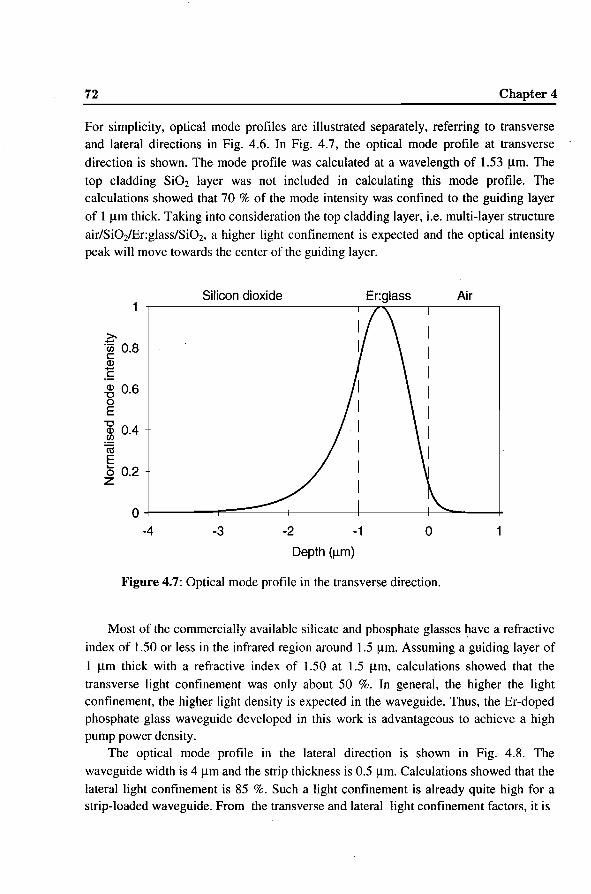
72 Chapter 4
For simplicity, optical mode profiles are illustrated separately, referring to transverse
and lateral directions in Fig. 4.6. In Fig. 4.7, the optical mode profile at transverse
direction is shown. The mode profile was calculated at a wavelength of 1.53 !J.m. The
top cladding Si02 layer was not included in calculating this mode profile. The
calculations showed that 70 % of the mode intensity was confined to the guiding layer
of 1 !J.m thick. Taking into consideration the top cladding layer, i.e. multi-layer structure
air/Si02/Er:glass/Si02, a higher light confinement is expected and the optical intensity peak will move towards the center of the guiding layer.
Silicon dioxide Er:glass Air
>. -ëii 0.8 c Q) -c Q) 0.6 '0 0 E '0 0.4 Q)
.~ ëij E .... 0.2 0 z
0 -4 -3 -2 -1 0
Depth (!lm)
Figure 4.7: Optical mode profile in the transverse direction.
Most of the commercially available silicate and phosphate glasses have a refractive
index of 1.50 or less in the infrared region around 1.5 !J.m. Assuming a guiding layer of
I !J.m thick with a refractive index of 1.50 at 1.5 !J.m, calculations showed that the
transverse light confinement was only about 50 %. In general, the higher the light confinement, the higher light density is expected in the waveguide. Thus, the Er-doped phosphate glass waveguide developed in this work is advantageous to achieve a high pump power density.
The optica! mode profile in the lateral direction is shown in Fig. 4.8. The
waveguide width is 4 J.lm and the strip thickness is 0.5 !J.m. Calculations showed that the
lateral light confinement is 85 %. Such a light confinement is already quite high for a strip-loaded waveguide. From the transverse and lateral light confinement factors, it is
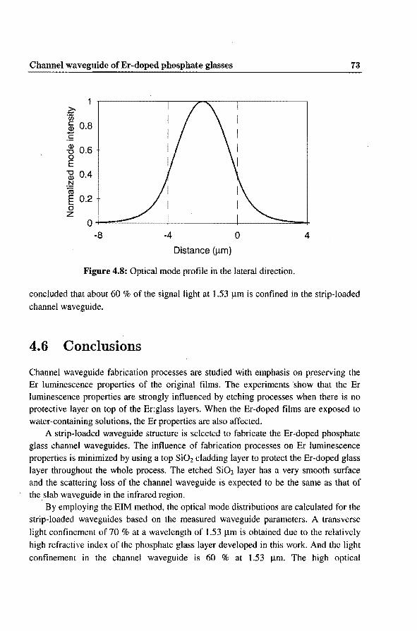
Channel waveguide of Er-doped phosphate glasses
1 >. -(i) c 0.8 (J) -c (J)
0.6 "0 0 E -g 0.4· -~ (ij
ê 0.2 0 z
o~~~----~--------~----~~~
-8 -4 0 4
Distance (!lm)
Figure 4.8: Optica! mode profile in the lateral direction.
73
condurled that about 60 % of the signa! light at 1.53 11m is confined in the strip-loaded
channel waveguide.
4.6 Conclusions
Channel waveguide fabrication processes are studied with emphasis on preserving the Er luminescence properties of the original films. The experiments show that the Er
luminescence properties are strongly influenced by etching processes when there is no proteelive layer on top of the Er:glass layers. When the Er-doped films are exposed to
water-containing solutions, the Er properties are also affected. A strip-loaded waveguide structure is selected to fabricate the Er-doped phosphate
glass channel waveguides. The influence of fabrication processes on Er luminescence
properties is minimized by using a top Si02 cladding layer to proteet the Er-doped glass
layer throughout the whole process. The etched Si02 layer has a very smooth surface and the scattering loss of the channel wavegulde is expected to be the same as that of
the. slab waveguide in the infrared region. By employing the EIM method, the optica! mode distributions are calculated for the
strip-loaded waveguldes based on the measured waveguide parameters. A transverse
light confinement of 70 % at a wavelength of 1.53 !liD is obtained due to the relatively
high refractive index of the phosphate glass layer developed in this work. And the light
confinement in the channel wavegulde is 60 % at 1.53 11m. The high optica!

74 Chapter 4
confinement of the waveguide is beneficia! to obtain a high pump power density, which is very important to realize the optical amplification in the waveguide.
Reference
[I] H. W. Lehmann, "Dry etching: concepts, methods and applications", in Physics and fabrication of microstructures and microdevices, ed. by M. J. Kelly and C. Weisbuch, Springer Verlag, 1986
[2] J. Shmulovich, A. Wong, Y. H. Wong, A. J. Bruce, W. H. Grodkiewicz and G. W. Berkstresser, "Deposition and characterization of Er-doped silicate films on silicon", Ceramic Transactions. 28, 369 (1992)
[3] D. R. Wolters, "On the oxidation kinetics of silicon: the role of water", J. Electrochem. Soc. 127, 2072 ( 1980)
[4] W. A. Pliskin, in "Semiconductor Silicon 1973", ed. by H. R. Huff and R. R. Burgess, Princeton N. J., 506 (1973)
[5] N. Yamaguchi and Y. Kokubun, Electron. Lett. 25, 128 (1989)
[6] M. K. Smit, "Integrated opties in silicon-based aJuminurn oxide", Ph.D. thesis, University of Delft, the Netherlands, p. 85 (1991)
[7] J. R. Reitz, F. J. Milford and R. W. Christy, "Foundation of electromagnetic theory", (Addison Wesley, Reading, 3rd ed), chapter 16 (1979)
[8] H. Kogelnik, "Theory of dielectric waveguides", in Guided wave optoelectronics, ed. by T. Tamir (Springer Verlag, Berlin, 2nd ed.), 1990
[9] H. Nishihara, M. Haruna and T. Suhara, "Optica! integrated circuits", (McGraw Hill, NewYork), 1989
[10) G. J. M. Krijnen, "All-optical switching in nonlinear integrated optie devices", Ph.D. thesis, University of Twente, the Netherlands, (1992)
[11] H. M. K. K. Koerkamp, "An integraled-optic intensity modulator based on mode coupling", Ph.D. thesis, University of Twente, the Netherlands, p.28, 1992
[12] H. J. van Weerden, A computer program on slab waveguide model, Lightwave group, University of Twente, the Netherlands
[13] M. K. Smit, "Integrated opties in sîlicon-based aJuminurn oxide", Ph.D. thesis, University of Delft, the Netherlands, p. 68 (1991)
[14] T.H. Hoekstra, "Erbium-doped Y20 3 integrated optical amplifiers", Ph.D. thesis, University of Twente, The Netherlands, p. 160 (1994)

Chapter 5
Optica! amplification of Er-doped phosphate glass waveguides
5.1 Introduetion
Er-doped fiber amplifiers (EDFA's) with a high optica! gain have been developed by doping in si! i ca fiber with a low Er concentratio u [I]. In order to achieve optica! amplificat.ion in planar Er-doped optica! waveguide of a few centimeters long, the waveguide has to be highly doped with Er ions, typically about 100 times higher than in an EDFA. Two Er photoluminescence (PL) quenching processes deteriorate the Er PL efficiency undcr high Er concentration: an Er concentration quenching process and an cooperative upconversion queuehing process. The Er concentration queuehing process in Er-doped phosphate glasses was discussed in Chapter 2.
In thîs chapter, the optica! amplification properties of the Er-doped phosphate glass waveguides will be presented. And the cooperative upconversion quenching process in the Er-doped waveguide amplifier is studied by modeling the measured data.
At first, Er3+ absorption cross sections and emission cross sections are derived from
the Er attenuation spectrum in the waveguide, which will be used in the waveguide gain model. The Er attenuation spectrum was measured in a two-prism coupling set-up. Two-prism coupling measurements have been used to evaluate the waveguide background Ioss in the infrared region (see Chapter 3) and here the measuring set-up will bedescribed only briefly.
Next, the optica! gain measurement set-up will be described. A 980 nm light beam emitted from a Ti:sapphire laser is used as pump light. The experimental results of the gain measurements are simulated by rate equations involving the cooperative upconversion quenching process, as well as the evolution of the signa] and pump light along the length of the waveguide. Furthermore, possible improvements of the Erdoped waveguide amplifiers are presented, by using modeling calculations taking into account waveguide length, Er luminescence lifetime, Er concentration, and waveguide background loss.

5.2 Absorption cross sections and emission cross sections of El+
5.2.1 Two-prism coupling metbod
The attenuation spectrum of the planar waveguide was measured by two-prism coupling method, from 600 nm to 1600 nm [2]. Theset-upis shown in Fig. 5.1.
incoupling moving fiber bundie
..Q.-----11 spedrom<rer I:
Figure 5.1: A two-prism coupling set-up for measuring the waveguide attenuation loss spectrum.
A tongsten lamp with a collimator was used as a light source. The converging polarized polychromatic light beam was coupled by a prism to the propagating fundamental TE mode of the waveguide. The mode was coupled out by a second prism, and the transmitted spectrum was analyzed with a spectrometer. From a set of waveguide transmission spectra, recorded at various prism separations, the waveguide attenuation spectrum can be determined. A waveguide attenuation spectrum from 700 nm to 1600 nm is shown in Fig. 5.2.
In Fig. 5.2, the three absorption bands visible at 0.8 Jlm, 0.98 Jlm and 1.53 Jlm, are due to the Er dopants. A detailed analysis [3] of waveguide attenuation mechanisms revealed that the measured spectrum was a superposition of Rayleigh scattering, the UV absorption edge and the Er absorption bands. The attenuation loss at 1.3 !liD, where
there is no Er absorption, denotes the waveguide background loss at the near-infrared range. In Fig. 5.2, the waveguide backgroundlossis- 1.8 dB/cm. As shown insection 3.4, the optimized waveguide bas a background loss of 0.9 dB/cm, see again Fig. 5.3.

Optical amplification ofEr-doped phosphate glass waveguides
-E ~ co ~ {/) {/) 0
...J (ij ()
a 0
10
8
6
4
2
0.7 0.8 0.9 1.1 1.2 1.3 1.4 1.5 1.6
Wavelength ( 1Jffi)
Figure 5.2: An attenuation spectrum of an Er-doped planar phospbate glass waveguide measured by the two-prism coupling metbod (This spectrum was also shown in Fig. 3.6).
5.2.2 Results and discussion
71
In order to model and to optimize tbe waveguide amplification properties, the absorption and emission cross sections of Er3
+ are important parameters. Absorption cross sections of Er3
+ can be calculated from the Er absorption spectra, measured by two-prism coupling metbod on a planar waveguide. Emission cross sections can be derived from the absorption cross sections using the McCumber theory [4], also known as a metbod ofreciprocity.
The Er absorption spectrum around 1.53 tJm as shown in Fig. 5.3 is used to
calculate the Er absorption cross sections, based on the following formula:
ln(lû) <XEr (J =-----
a 10 f'·NEr (5.1)
where CXEr is the Er absorption (<XEr. in unit of dB/cm) as sbown in Fig. 5.3 after
subtraction of the estimated background loss, NEr is Er concentration and r is the
confinement of light to the Er doped region.

78 Chapter 5
10
Ê 9 T
as 8 t
:s 7 c: 6 0
~ 5-0 (/) 4 ..0 (Ó
.(ij 3 (.)
+:::: 2 a. 0
1
0 1100 1200 1300 1400 1500 1600
Wavelength (nm)
Figure 5.3: Attenuation spectrum for an optimsed Er-doped waveguide, which shows a background loss of 0.9 dB/cm. The Er absorption at 1.53 J.lm after subtraction ofthe backgroundlossis about 8.7 dB/cm.
With NEr 5.3 x 1020 cm'3 calculated from the XPS measurement and r = 70 %,
which is calculated in Chapter 4 (see Fig. 4.7), the Er absorption cross section around
1.53 pm is calculated and shown in Fig. 5.4. The peak absorption crosssectionat 1.535
pm is 5.3 x 10'21 cm2• The dasbed line in Fig. 5.4 is an extrapolation line since the Er
absorption should decrease to almost zero at around 1.65 J.lm.
The emission cross section can be calculated by McCumber theory [4,5]. The
emission cross section, Ciemfv), at a frequency v, is related to the absorption cross section
cra(v):
z Cie(v) = cra(V)-1 exp[(EZL- hv)l kT]
Zu (5.2)
Where Zu and Z1 are the partition functions of upper and lower state, EzL is the energy difference between the bottorn of the upper state manifold and bottorn of the ground state manifold ( the so-called zero-line energy), T is temperature and k is Boltzmann's constant. The only assumption in this theory is that the time to establish thermal equilibrium in each manifold is short compared to the lifetime of the manifold, which is the case for the 411312 -
411512 transitionsof Er3+ in phosphate glass films.

Optical ampllfication ofEr-doped phosphate glass waveguides
6
5
-C\1 4 E ~(.)
C}l 0 3 ,.....
fJl ..0 2 b<\1
... 0 +-----~r------+------~------~---~-~~ 1400 1450 1500 1550 1600 1650
Wavelength (nm)
Figure 5.4: Absorption cross section spectrum forthe 411312 ~ 411512 transition
in Er-doped phosphate glass waveguide, as determined from prism coupling measurements (solid line). The dasbed line is an extrapolation.
6
5
C\1-4 E
"..u C}l 0 3 ,.....
E ~ 2
1
0 1400 1450 1500 1550
. . . . . .
Wavelength (nm)
........... "' ....... . . .
1600 1650
Figure 5.5: Calculated Er.H stimulated emission cross section spectrum. The dasbed line is a measured Er luminescence spectrum, scaled to the calculated emission spectrum.
79

80 Chapter 5
The following values were used to calculate the Er3+ emission cross section:
ZtfZu - 1
EzL = 6515 cm·1 => 0.81 eV k = 1.38 x 1 o-23 JtK h = 6.63 x 1 o·34 J sec T = 300K
The calculated emission cross section spectrum is shown in Fig. 5.5. The measured Er luminescence spectrum is also shown in the same figure, scaled to the calculated emission spectrum. In · general, the two spectra are in good agreement in the range of 1400 nm- 1560nm.
5.3 Optical amplification
5.3.1 Measurement set-up
Optical amplification measurements were performed on a strip-loaded waveguide (see
Chapter 4) by coupling a signal beam at 1.535 ,urn in the waveguide, in actdition to the pump beam at 980 nm (see Fig. 5.6). The channel waveguide under study was 10 mm
long and had a cross section of l 11m in height and 4 11m in width. The background loss
was 0.9 dB/cm at 1.3 11m and the Er absorption was about 8.7 dB/cm at 1.53 11m
measured by two-prism coupling (see Fig. 5.3). The Er concentration was about 5.3 x I 020 cm·3
, as calculated from XPS measurements.
chopper • controller•
Figure 5.6: A set-up for optical gain measurements of Er-doped waveguides.

Optica! amplification of Er-doped phosphate glass waveguides 81
The 980 nm pump light was provided by a Ti:sapphire laser, which was pumped by an Ar ion laser beam at 488 nm. The Ar laser had a maximum output power of 7 W, and 200 mW 980 nm light was emitted from the Ti:sapphire laser, of which about 33 % was coupled into a single-mode fiber (SMF). The signa! beam, emitted from an external
cavity diode laser operating at 1.535 11m, was chopped by a mechanica! chopper before it was coupled into a single-mode fiber. The signa! power was below -40 dBm ( < 0.1
J1W). Pump and signa! were combined by a 980 nm/1530 nm wavelength division multiplexer. The mixed beam was senttoa power splitter, where a 2% reference signa! of the splitter output, was monitored by a power meter and an optica! spectrum analyzer. The 98 % main output of the splitter was coupled into the waveguide with a tapered optica! fiber, which was aligned by means of piezo actuators.
At the waveguide output end, the light was collected by a microscope objective and was then coupled to a single mode fiber. The output signa! was speetrally analyzed by a single-grating monochromator and was detected by a liquid-nitrogen-cooled Ge
detector. Finally, the signallight at 1.535J1m was recorded using a lock-in amplifier.
5.3.2 ltesults and discussion
en -30 ~ z-. ëii c: Q) -40 ~ (ij ()
a 0 -50
-60 +-----+----+-----+----+-------1
976 976.5 977 977.5 978 978.5
Wavelength (nm)
Figure 5. 7: Spectrum of pump light around 977.3 nm used in the gain measurement .
The spectrum of the pump light used in the measurement is shown in Fig. 5.7, which is a sharp peak centered at 977.3 nm. This pump wavelength coincides with the Er

82 Chapter 5
absorption peak due to the Er3+ transition 411512 ___,
4l 1112 around 0.98 J.tm, as shown in
Fig. 5.2.
The amplified spontaneous emission (ASE) spectrum in the 1.5 Jlm was measured
by an optica! spectrum analyzer, as shown in Fig. 5.8. The ASE spectrum from 1450 nm to 1650 nm has a shape resembling the Er photoluminescence spectrum. The sharp peak around 1535 nm is due totheEr stimulated emission.
-50 ,-------------------,
-60 -
iD :3. -70 :è' <I) c: (!) -80 :5 (ij
.g -90
8" -100 il
-110 +-----t----i---t----+---+----'
1250 1350 1450 1550 1650 1750
Wavelength (nm)
Figure 5.8: Measured Er ASE spectrum and stimulated emission at 1.53 J.tm.
The enhancement of the 1.53 Jlm optical signal intensity as a function of pump
power in the input fiber was measured, and is shown in Fig. 5.9. The pump light intensity in the input fiber was calculated from the measured reference light. Fig. 5.9 shows that as the pump power is increased, the signa! rapidly increases; An signa) enhancement of 13.7 dB is reached at a pump power of 66 mW in the fiber.
The fiber-to-waveguide coupling was not optimized and the coupling efficiency was estimated to be - 30 % by collecting pump power from the output end of the waveguide. The second x axis in Fig. 5.9 denotes the estimated pump power in the waveguide. The signa! enhancement data were converted to net optical gain (right vertical a:x.is) by setting the gain at zero pump power, equal to the measured Er
absorption at 1.53 J.tm (8.7 dB) plus the known waveguide loss (0.9 dB). Net optical gain is reached at a pump power of- 20 mW intheinput fiber, equal to-- 7 mW in the

Optical amplification ofEr-doped phosphate glass waveguides
Pump power in waveguide (mW)
0 5 10 15 20
14 4
3 12 2
00 • -o • -:::: 10 '- 0 c: 00 Q)
-1 E • ::g_ Q) 8 (.) • -2 c: c: (ij (Ij -3 Cl J:: c: 6 Q) Q) -4 z (ij
-5 c: Cl
Ü) -6 -7
2 -8 -9
00 10 20 30 40 50 60 70 80
Pump power in input fiber (mW)
Figure 5.9: Measurements of the optica! signa! enhancement at 1.53 Jlm in a l 0 mm long Er-doped phosphate glass waveguide amplifier as a function of 980 nm pump power (• experimental data). The solid line represents the calculated gain curve as explained in the text.
83
waveguide. At a pump power of 66 mW in the fiber, a net (small-signal) optica! gain of 4.1 dB at 1.53 Jlm is achieved for the 10 mm long waveguide; this refers to an optica! gain tigure of 4.1 dB/cm. To our knowledge, this is the highest optical gain per unit length reported in the literature as yet for an Er-doped planar waveguide amplifier with 66 mW pump power in the fiber (or -20 mW in the waveguide).
5.4 U peonversion in the waveguides
As discussed in chapter 1 and chapter 2, the dominating quenching mechanism for planar waveguide amplifiers is a cooperative upconversion process. The upconversion process can be characterized by an upconversion coefficient, which is a material related factor. By measuring the waveguide amplification properties, this quenching process can be studied by determining the upconversion coefficient.

84 Chapter 5
As no 800 nm or 980 nm emission is observed, the lifetime of the 4/ 912 and 4
/ 1112
manifolds are thought to be short. In this case, rate equations for a two-level system [6,7] can be used to describe the fraction n2 of Er3+ ionsin the upper lasing 4
/ 1312 level, with pumping into the 980 nm band :
(5.3)
Here, ris the spontaneous decay time resulting from radiative and non-radialive decay
for the case without upconversion, R12 is the rate of absorption of 980 nm pump light, p
is the Er concentratioÓ, C the homogeneous upconversion coefficient. The effect on n2
due to amplification of spontaneous emission (ASE) is neglected. Upconversion is described by a quadratic term, as it involves two excited Er ions. The following
relations was used: R12 lva.fhvp, where hvp is the pump pboton energy, a. is the absorption crosssectionat 980 nm, and lp the pump intensity which is estimated using a
waveguide cross section of 1 J.im by 4 11m. At the steady state, the fraction of Er in the excited level can be derived from Eq.
(5.3), by setting dn2/dt = 0. The following expression is obtained:
(5.4)
From this expression, it is clear that the higher the upconversion coefficient C, the smaller the fraction of Er intheupper level, fora given pump intensity.
Once the n2 is known, the pump and signa! light in the waveguide can be modeled by employing an optica! propagation model [8,9]. The evolution of the pump intensity lp along the z-axis (light-propagation direction) in the waveguide is determined by a
differential equation which consists of contributions from the waveguide loss (a, in units of cm-1
), and absorption due to Er3+:
d/p ( ) --=-al -a a 1- n2 I pr dz P P P P
(5.5)
After inserting Eq. (5.4) in Eq. (5.5), the solution /p(Z) can be found by numerical integration. From /p(Z), the fraction n2 of excited Er3+ can be determined everywhere in the waveguide by Eq. (5.4).
It is thus possible to determine the signa! evolution. Starting from the differential equation for the signa! intensity /s(z), which is similar to Eq. (5.5), using in this case the
emission and absorption cross sections at the signa! wavelength, the gain function g(z) = ln[/8(Z)/ls(O)] is found:

Optica! amplification of Er-doped phosphate glass waveguides 85
(5.6)
In optica! telecommunication, the optica] gainis usually defined as G(z) in dB, which is related to g(z) by:
( 18 (Z)J 10
G(z)=l0log10 -- =--g(z) [dB] /
8(0) ln(IO)
(5.7)
Basedon Eq. (5.3)- (5.7), the optica! gain of a waveguide versus pump intensity can be calculated. All the parameters in the above equations, except the upconversion coefficient C, have been determined experimentally in this thesis, and are shown in Table 5.1.
Table 5.1 Parameters of the waveguide amplifiers used in the calculations
Er lifetime without upconversion r 4 ms Er concentration (llcm3
) p 5.3 x 1020 cm·3
cooperative upconversion coefficient c 2 x 10"18 cm3/s Pump absorption cross section (980 nm) apa 2.2 x 10"21 cm2 [12]
Signa! absorption cross section (l.53!lm) a.a 5.39 x 10"21 cm2
Signal emission cross section (1.53 !liD) a.e 5.39 x 10"21 cm2
waveguide loss a 0.9 dB/cm Optica! mode size 1 f.lm x 4 f.lm Overlap mode intensity (at 0.98 f.lm) withEr profile rP 65% Overlap mode intensity (at 1.53 f.lm) with Er profile r. 60 %
By fitting the calculated gain figures to the measured gain data, as shown in Fig.
5.9, the (uniform) cooperative upconversion coefficient is determined to be C = (2.0 ± 0.5) x 10"18 cm3/s, which is also listed in Table 5.1.
Compared with other studies [ 6,7, 10,11], the Er3+ upconversion coefficient of the phosphate glass is one of the lowest among known Er host materials. A high upconversion coefficient of - 10"16 cm3/s is reported for highly Er-doped Ge/Al/Pdoped fused silica fibers [6]. For Er-doped P/Al co-doped silica, the upconversion
coefficient is estimated to be 10 x 10"18 cm3/s [ 10], by calculating the speetral overlap
between the 1.5 f.liD emission and 1. 7 f.lm excited-state-absorption cross sections. However, a much higher upconversion coefficient has to be assumed in order to match the measured gainlpump curve in that study. Furthermore, the Er+ upconversion
coefficient is determined to be 3 x 10"18 cm3/s for an Er-implanted sodalime glass, which is a multi-component silicate glass [7].

86 Chapter 5
Since the upconversion process is the dominant queuehing process of the Er luminescence, the low upconversion coefficient figure, determined in this study shows that the multi-component phosphate glass is a very good Er host in view of the application of planar waveguide amplifiers.
5.5 Optimization of an Er-doped phosphate glass waveguide amplifier
The upconversion coefficient of the Er-doped phosphate glass waveguide, determined in the last section, is assumed to be a material-related property. The relatively low upconversion coefficient of the present Er-doped phosphate glass suggests that an efficient Er-doped planar waveguide amplifier is obtainable. Net optica] gain was demonstraled in a 10 mm long waveguide.
In this section, effects of other parameters which influence the optica! gain of the Er-doped waveguide, wil! be studied, based on the model presented in the last section, including waveguide length, Er concentration, Er lifetime, background loss and fiberwaveguide coupling efficiency. The calculations are based on the known waveguide parameters listed in Table 5.1. The pump wavelength is 980 nm and the signa1
wavelength is 1.535 j.lm.
Optimization of waveguide length
Modeling calculations are carried out to study the optimized waveguide length for optica! gain. Fig. 5.10 shows the ca1culated gain behavior fora 4-cm Jong waveguide. The measured datafora 1-cm long waveguide and the theoretica! fittothese data (cited from Fig. 5.9) are also shown in Fig. 5.10. Besides the waveguide length, the other parameters used in this calculation, are kept the same.
The optica! gain for the 1-cm long waveguide starts to saturate at a pump power of 30 mW, whereas the optica! gain for the 4-cm long waveguide still increases at a pump power of 100 mW. With a high pump souree available at 980 nm, a high optica! gain can be reached for a 4-cm long waveguide; more than 15 dB gain is obtainable with a pump power of 40 mW. With a 60 mW pump intensity, the gain will increase to 20 dB.
For a given background loss, the optimized waveguide length is dependent on the pump power in the waveguide. The dependenee of the optimized waveguide length on the pump power available in the waveguide, is shown again in Fig. 5.ll. A maximum gain of 6.9 dB can be obtained fora waveguide lengthof 2.8 cm at a pump power of 20 mW. At a waveguide length of 4 cm, 11.8 dB gain is obtainable at a pump power of 30 mW.A net gain of20 dB can be achieved with a waveguide of 4.9 cm longand a pump
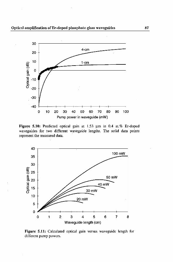
Optica! amplification of Er-doped phosphate glass waveguides
30
4-cm 20
co 10
:3. c: 0 ëii Ol
~ -10 a 0 -20
-30
-40 +---+--t---+--+---+--+--+---+---+-----1
0 1 0 20 30 40 50 60 70 80 90 1 00
Pump power in waveguide (mW)
Figu~e 5.10: Predicted optica) gain at 1.53 11m in 0.4 at.% Er-doped waveguides for two different waveguide lengths. The solid data points represent the measured data.
40 100mW
35
30 co :3.25 c: -~20 (ij
.g 15 a. 0
10
5
0
0 2 3 4 5 6 7 8
Waveguide length (cm)
Figure 5.11: Calculated optica! gain versus waveguide length for different pump powers.
87

88 Chapter 5
power of 50 mW. Furthermore, a 35 dB gainis predicted at 100 mW pump powerfora 8-cm long waveguide.
Effect of Er luminescence lifetime
The Er luminescence lifetime of the waveguide used for the gain measurement is 4 ms. The Er tifetime bere refers to the measured Er lifetime without the upconversion quenching effect, e.g. measured at a low pump intensity. In Chapter 4, we have shown the influence of the channel waveguide fabrication process on the Er lifetime; in principle, an Er lifetime of 7-8 ms is possible and in the worst case the Er lifetime is only about 1-2 ms. The influence of the Er lifetime on the optica! gain is shown in Fig. 5.12.
In Fig. 5.12, the calculated optical gain of an Er-doped glass waveguide is shown for an assumed lifetime of 1 ms, 4 ms and 7 ms, respectively. The gain curve of 7 ms is slightly different from the gain curve of 4 ms; at the high pumping region, the two curves tend to overlap. This phenomenon shows that the upconversion queuehing process is dominant at the high pumping region. When Er lifetime deercase from 7 ms to 4 ms, the gain threshold increases only 1.5 mW (from 12.8 mW to 14.3 mW).
30 ~~~~~--------------------------~
20
-30
-40
I I
I
/ / . /
/ I
I
....... ----
0 1 0 20 30 40 50 60 70 80 90 1 00
Pump power in waveguide (mW)
Figure 5.12: Influence of Er luminescence lifetimes on the optica! gain of a 4-cm long waveguide.

Optica! amplification of Er-doped phosphate glass waveguides 89
However, when the Er lifetime decrease to 1 ms, as shown in Fig. 5.12, the gain curve is significantly different from the gain curves of 7 ms; The gain threshold increases to 24.8 m W, almost two times of that for gain curve of 7 ms. Furthermore, a much higher pump power is needed to reach the gain saturation; at 100 mW pumping, the optica! gainis still 3 dB lower than for the others.
Fig. 5.12 shows that the upconversion processis the dominant quenching process at high pumping intensity. However, a too low Er lifetime (1-2 ms), will lead to a significant increase of the pumping threshold.
Optimization of Er concentration in the waveguide
In general a high Er concentration is necessary fora planar waveguide amplifier, due to its short optica! length. In Fig. 5.13, the calculated optica! gain curves for three
different Er concentrations, 2.5 x 1020 cm·3, 5.3 x 1020 cm·3 and 7.5 x 1020 cm·3, are
depicted. In the calculation, the Er lifetime is assumed to be 4 ms for all three different Er concentrations. The assumed waveguide length is 4 cm.
40 ,-----------------------------------,
30
20
iD 10 ~ c:: 0 til O'l·10 (ij ~ -20 c. 0 -30
-40
-50 .
' ' ' . ; I • I I
I
/ 7.5 x 1020cm3 I
5.3 x 1020cm·3
2.5 x 1 020cm3
·60 -~-+--~--~~--~--+-~---+--~~
0 1 0 20 30 40 50 60 70 80 90 1 00
Pump power in waveguide (mW)
Figure 5.13: Optica! gain versus pump power for three Er concentrations, 2.5 x 1020 cm·3
, 5.3 x 1020 cm·3, and 7.5 x 1020 cm·3
•
The Er lifetime of 4 ms is used for all the three Er concentrations. The waveguide length is assumed to be 4 cm.
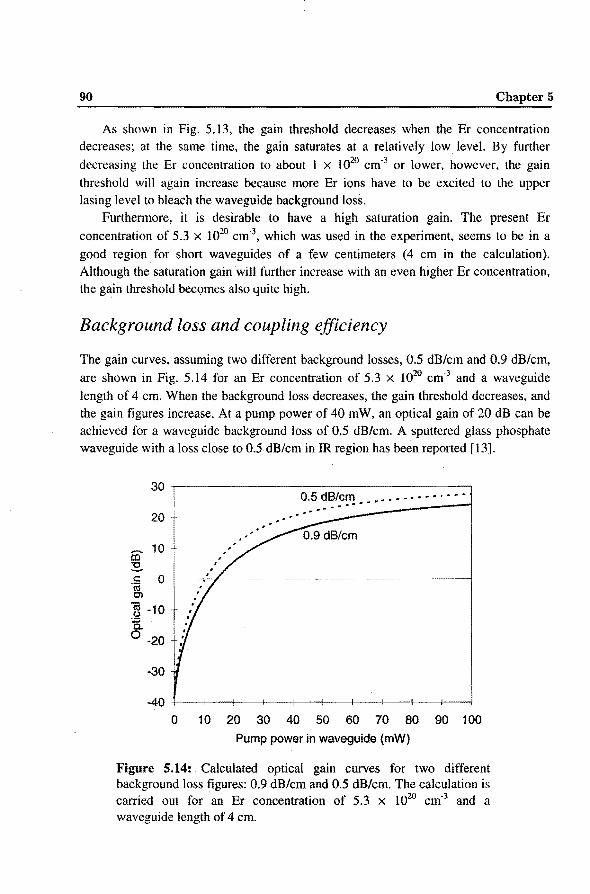
90 Chapter 5
As shown in Fig. 5 .13, the gain threshold deercases when the Er concentration decreases; at the same time, the gain saturates at a relatively low level. By further
decreasing the Er concentratien to about 1 x 1020 cm·3 or lower, however, the gain
threshold wil! again increase because more Er ions have to be excited to the upper lasing level to bieach the waveguide background loss.
Furthermore, it is desirabie to have a high saturation gain. The present Er
concentratien of 5.3 x 1020 cm·3, which was used in the experiment, seems to be in a
good region for short waveguides of a few centimeters (4 cm in the calculation}. Although the saturation gain wil! further increase with an even higher Er concentration, the gain threshold bec()mes also quite high.
Background loss and coupZing efficiency
The gain curves, assuming two different background losses, 0.5 dB/cm and 0.9 dB/cm,
are shown in Fig. 5.14 for an Er concentratien of 5.3 x 1020 cm·3 and a waveguide
length of 4 cm. When the background Joss decreases, the gain threshold decreases, and the gain figures increase. At a pump power of 40 mW, an optica! gain of 20 dB can be achieved for a waveguide background loss of 0.5 dB/cm. A sputtered glass phosphate waveguide with a loss close to O.SdB/cm in IR region has been reported [13].
30 ,---------------------------------,
20
10 éil ~
0.5 dB/cm •••.•• - • • • · • - • --~-----1
c 0 , ____ ~, _____ ----- ---~--~---~--~-------~ (ij OI
'B -1o a 0 ·20
·30
-40 +---~~---+--~--~--+---+-~~~--~
0 10 20 30 40 50 60 70 80 90 100
Pump power in waveguide {mW)
Figure 5.14: Calculated optica! gain curves for two different background loss figures: 0.9 dB/cm and 0.5 dB/cm. The calculation is carried out for an Er concentration of 5.3 x 1020 cm·3 and a waveguide Jength of 4 cm.

Optical amplification ofEr-doped phosphate glass waveguides 91
From the above calculations, we can see that a high pump power is desired in order to achieve a high optica! gain. Fiber-to-waveguide coupling efficiency is an important factor in order to make full use of the pump power. At the moment, the coupling efficiency is estimated to be - 30 %. The coupling efficiency may be further increased by ha ving a tapered fiber optimized for the waveguide structure used.
5.6 Conclusions
A net optica! gain of 4.1 dB was measured in a 10 mm long Er-doped phosphate glass waveguide amplifier with a pump power of 66 mW intheinput fiber at 980 nm (- 20 mW in the waveguide). The Er-doped waveguides were fabricated by RF-sputtering techniques on thermally oxidized silicon substrates. By camparing the measured gain
data with calculations, an upconversion coefficient of 2 x 10"18 cm3/s is determined,
which is one of the Jo west as compared to those of other known Er glass host materials. The cooperative upconversion process is the dominant Er luminescence queuehing
process in Er-doped optica! amplifiers, which is strongly dependent on the Er doping level in the device. While in an Er-doped fiber amplifier (EDFA), the upconversion queuehing process does not occur due to its low Er doping, we have shown that the effect of the upconversion process can be minimized by choosing a multicomponent phosphate glass with a high Er doping. Thus, consiclering the Er luminescence efficiency, an Er-doped planar waveguide amplifier as efficient as its fiber counterpart can be expected.
Simulations to further optimize the Er-doped waveguide amplifier design were conducted. It is demonstrated by calculations that a net gain of 20 dB is achievable for a 4-cm long waveguide with a pump power of 60 mW in the waveguide. In addition, calculations show that it is feasible to achieve an optica! gain of more than 35 dB with a pump power of 100 mW at 980 nm in the waveguide, by extending the phosphate glass waveguide to a length of 8 cm. The realised and predicted gain figures are very promising for large-scale application of planar Er-doped waveguide amplifiers in optica! telecommunications systems.
Reference
[1] N. Kagi, A. Oyobe and K. Nakamura, "Efficient optica! amplifier using a Jowconcentration erbium-doped fiber", IEEE Photon. Techno!. Lett. 2, 559 ( 1990)
[2] T. H. Hoekstra, "Erbium-doped Y20 3 integrated optica! amplifiers", Ph.D. thesis, University of Twente, The Netherlands, p. 134 (1994)

92 Chapter 5
[3] T.H. Hoekstra, "Erbium-doped Y20 3 integrated optica! amplifiers", Ph.D. thesis, Ph.D. thesis, University of Twente, The Netherlands, chap. 6, p. 163 (1994)
[4] W. J. Miniscalo and R. S. Quimby, Opt. Lett. 16,258 (1991)
[5] S. A. Payne, L. L. Chase, L. K. Smith, W. L. Kway and W. F. Krupke, IEEE J. Quanturn Electron. 28, 2619 ( 1992)
[6] P. Blixt, J. Nilsson, T. Carlnäs and B. Jaskorzynska, "Concentration-dependent upconversion in Er3+-doped fiber amplifiers: Experiments and modeling", IEEE Photon. Techno!. Lett. 3, 996 (1991)
[7] E. Snoeks, G. N. van den Hoven, A. Polman, B. Hendriksen, M. B. J. Diemeer, F. Priolo, "Cooperative upconversion in erbium implanted sodalime silicate glass optica! waveguides", J. Opt. Soc. Am. B 12, 1468 (1995)
[8] M. J. F. Digonnet, IEEE J. Quanturn Electron. 26, 1788 (1990)
[9] E. Snoeks, "Optica! doping of silica by erbium ion implantation", Ph.D. thesis, Utrecht University, The Netherlands, chap. 6, p. 80 (1995)
[I 0] J. E. Roman, M. Hempstead, C. Y e, P. Camy, P. Laborde and C. Lerminiaux, "1. 7 !J.m excited state absorption measurement in erbium-doped glasses", Appl. Phys. Lett. 67, 470 (1995)
[ll] G. N. van den Hoven, E. Snoeks, A. Polman, C. van Dam, J. W. M. van Uffelen and M. K. Smit, "Upconversion in Er-implanted Ah03 waveguides", J. Appl. Phys. 79, 1258 (1996)
[12] ap" = 2.2 x 10'21 cm2 at 980 nm, estimated by Eq. (5.1) in this chapter and an Er absorption of 3.8 dB/cm at 980 nm (see Fig. 5.2);
W. J. Miniscalo, J. Lightwave Techno!. 9, 234 (1991)
[ 13] G. R. J. Robertsou and P. E. Jessop, "Optica! waveguide laser using an rf sputtered Nd:glass film", Appl. Opties. 30, 276 (1991)

Sumn1ary
Currently, there is astrong interest indeveloping planar waveguide amplifiers at 1.5 IJ.m
with small dimensions of only a few centimeters. Planar waveguide amplifiers have potential applications in optica) telecommunication and signa! processing systems as
integrated devices.
Trivalent Er is the only lasing ion which gives a light emission around 1.53 J.lm
under suitable pumping due to the Er3+ intra-4f optica! transitions. Phosphate glasses
have proved to be good optica! glasses, which have a high solubility for Er. Thus
phosphate glasses are selected as Er hosts in this study. For planar optica! wavegulde amplifiers, due to their short optica! paths, a high Er concentration and a high pump power
density are needed to obtain sufficient optica! amplification. Therefore, the first challenge of this study is to achieve an efficient luminescence in highly Er-doped phosphate
glasses. RF-sputtering techniques are applied to produce Er-doped phosphate glass
waveguides on silicon substrates. The most important properties of a wavegulding medium are the attenuation loss and the refractive index. Thus, the second challenge of this study is to fabricate a low loss Er-doped phosphate glass wavegulde by RFsputtering techniques, at the same time preserving the efficient Er luminescence
properties at the optica! transition of 1.53 IJ.m.
In Chapter 2, preparation and optimization of Er-doped phosphate glasses are
discussed. Efficient Er photoluminescence (PL) properties are obtained in highly (up to 4 mole % Er20 3) Er-doped phosphate glasses. After a special heat-treatment with the
as-melted samples, the PL lifetime of Er ions for the 411312 -411512 transition increases
substantially, typically from 1-2 ms up to 7 ms for a sample doped with 2 mole %
Er20 3. The increase of the lifetime is ascribed to a decrease in concentration of hydroxyl groups incorporated in the glass, which is confirmed by IR absorption spectroscopie measurements. The luminescence concentration quenching mechanism by hydroxyl groups is modelled using electric dipole - dipole interaction theory. The
model is found to be in good agreement with the experimental results. The development of planar optica! waveguides based on Er-doped phosphate
glasses is presented in Chapter 3. RF-sputtering deposition processes of Er-doped
phosphate glasscs on thermally oxidized silicon wafers are studied. The optimized Erdoped phosphate glass disks are used as the sputtering targets. The films are deposited

94 Summary
in an 0 21 Ar atmosphere at a low pressure. The optica! properties of the sputtered film, its attenuation loss and refractive index as well as the Er3
+ luminescence properties, are
optimized in view of the application as waveguide amplifiers at 1.53 )lm. A waveguide
background loss as low as 0.9 dB/cm has been achieved in the infrared region. Postannealing of the as-deposited films in pure oxygen is found to be effective to improve Er3
+ luminescent properties in the waveguide. The experiments described in Chapter 4 show that the Er luminescence properties
may be influenced by the fabrication processes, invalving photolithography and etching. A strip-loaded waveguide structure is applied to fabricate the Er-doped phosphate glass channel waveguides, with a minimized influence on Er luminescence properties. The optica! mode distributions are calculated for the strip-loaded waveguides, based on the measured waveguide parameters.
In Chapter 5, the optica! characterization of the Er-doped phosphate glass waveguldes is discussed. The Er absorption cross section and stimulated emission cross section are deterrnined from the Er absorption spectrum measured by a two-prism coupling method. Optica! signa] enhancement measurements are conducted for a I 0 mm
long waveguide with a cross section of I )lm by 4 )lm. Net optica! gain of 4.1 dB at
1.535 )lm is achieved for the 10 mm long wavegulde with a pump power of 21 mW at
980 nm in the waveguide. The amplifying properties of the waveguide are modelled, taking into account the upconversion quenching process, and the upconversion
coefficient is determined to be 2 x 10"18 cm3/s. The upconversion coefficient of the
present Er-doped phosphate glass is one of the lowest as compared to other known Er host materials. Furthermore, the model shows that it is feasible to achieve an optica! gain of more than 20 dB with a waveguide of 4 cm long and a launched pump power of 60mW.
In conclusion, a comprehensive study has been conducted on the development of an
optica! waveguide amplifier at 1.5 Jlm, including material host optimization, device fabrication and optica] characterization. The results and the knowledge described in this thesis are of great significanee for optica! telecommunication and other related areas.

Samenvatting
De ontwikkeling van geïntegreerde planaire optische versterkers bij 1.5 J.l.ffi met afmetingen van slechts enkele cm • s, staat op dit moment sterk in de belangstelling. Planaire optische versterkers hebben belangrijke toepassingsmogelijkheden in optische telecommunicatie en signaalbewerkingssystemen als geïntegreerde optische componenten.
Driewaardig Er is het enige optisch actieve ion dat licht kan uitzenden rondom de 1.53 !Jffi door excitatie met een geschikte pompgolflengte dankzij de 4f-schil optische overgangen van Er3
+. Fosfaatglazen hebben uitstekende optische eigenschappen en een hoge oplosbaarheid voor Er-ionen. Daarom zijn in dit onderzoek fosfaatglazen uitgekozen als matrix-glas voor Er. In verband met de korte optische weglengte van planaire ~ptische versterkers is een hoge Er-concentratie en een hoog pompvermogen vereist voor voldoende optische versterking. Daarom is het eerste doel van dit onderzoek het bereiken van een efficiënte Er-fotoluminescentie in hoog-gedoteerde fosfaatglazen.
In deze studie zijn hoog-frequent (RF) sputtertechnieken gebruikt voor het aanbrengen van dunne fosfaatglaslaagjes op silicium substraten. De belangrijkste eigenschappen van een lichtgeleidend medium zijn de optische demping en de brekingsindex. Dus, het tweede doel van dit onderzoek is de bereiding van Ergedoteerde golfgeleiders van fosfaatglas met lage optische demping met behulp van RFsputtertechnieken. Hierbij moet het hoge rendement van de optische overgang van Er bij 1.53 J.l.ffi behouden blijven.
Gedoteerde fosfaatglazen met hoge Er-concentraties (tot 4 mol% Er20 3) zijn bereid met behulp van gangbare glassmelttechnieken (hoofdstuk 2). Nadat de aldus gesmolten glazen een speciale warmtebehandeling hebben ondergaan, neemt het fotoluminescentie-rendement van de Er optische overgang 411312
411512 substantieel toe: Dekarakteristieke levensduur van het eruitterende niveau neemt hierbij toe van typisch I à 2 ms tot 7 ms. De toename in levensduur wordt toegeschreven aan een afname van de concentratie van hydroxyl (OH)-groepen in de glasmatrix, hetgeen bevestigd is door infra-rood spectrale absorptiemetingen. Het mechanisme van de luminescentieconcentratiedoving is gemodelleerd, waarbij gebruik is gemaakt van de theorie van elektrische dipool-dipool interactie. Er is een goede overeenkomst gevonden tussen model en experimentele resultaten.

96 Samenvatting
De ontwikkeling van planaire optische golfgeleiders op basis van Er-gedoteerde fosfaatglazen wordt besproken in Hoofdstuk 3. Er-gedoteerde fosfaatglaslaagjes zijn aangebracht op thermisch geoxydeerde silicium substraten m.b.v. RF-sputterdepositieprocessen. Geoptimaliseerde Er-gedoteerde fosfaatglasschijven zijn gebruikt als sputtertargets. De lagen zijn aangebracht in een 0 2/Ar-atmosfeer bij lage druk. De optische eigenschappen van de gesputterde laag, de dempingsverliezen en de brekingsindex, als ook de Er3+-fotoluminescentie eigenschappen zijn geoptimaliseerd met het oog op toepassing als optische golfgeleider-versterker bij 1.53 J.lm. Het is gelukt een achtergronddemping in het nabije infrarood van slechts 0.9 dB/cm in de golfgeleider te realiseren. Het is gebleken dat door een warmtebehandeling van de aangebrachte laagjes in zuivere zuurstof de fotoluminescentie-eigenschappen van Er3+ aanzienlijk kunnen worden verbeterd.
De experimenten besproken in Hoofdstuk 4, laten zien dat de Er3+fotoluminescentie-eigenschappen beïnvloed kunnen worden door het fabricageproces, bestaande uit gangbare lithografische en ets-technieken. Voor de fabricage van Ergedoteerde optische 'kanaaltjes' van fosfaatglas is gekozen voor een 'strip-loaded' golfgeleider structuur. De ruimtelijke verdeling van de optische.modes is berekend voor de 'strip-loaded' golfgeleiders, op basis van de gemeten golfgeleider-parameters.
In Hoofdstuk 5 wordt de optische karakterisatie van de Er-gedoteerde golfgeleiders van fosfaatglas besproken. De Er absorptie cross-sectie en de cross-sectie voor gestimuleerde emissie zijn bepaald uit het Er-absorptiespectrum, dat gemeten is met behulp van een 2-prisma, in-en uitkoppelingsmethode. De optische versterkingsmetingen zijn uitgevoerd met een 10 mm lange golfgeleider van 1 Jlm bij 4 Jlm. Een
netto optische versterking van 4.1 dB bij 1.535 jlm is gerealiseerd voor de 10 mm lange
golfgeleider bij een (980 nm) pompvermogen van 21 mW in de golfgeleider. De optische versterkingseigenschappen van de golfgeleider zijn gemodelleerd, rekening houdend met 'upconversion' -processen. Door de theoretische voorspellingen te vergelijken met de experimentele gegevens, is de grootte van de 'upconversion'
coëfficiënt bepaald op 2 x I o-18 cm3/s. Deze waarde, voor het hier ontwikkelde Erfosfaatglas, is één van de laagste in vergelijking met andere bekende matrixmaterialen voor Er. Bovendien, de modelleringsresultaten voorspellen een netto optische versterking van meer dan 20 dB, te bereiken in een golfgeleider van 4 cm lang bij een pompvermogen van 60 m W in de golfgeleider.
Concluderend: Er is een uitgebreid onderzoek uitgevoerd voor de ontwikkeling van een planaire optische versterker bij 1.5 J.lm. Dit onderzoek omvat de optimalisatie van het matrixglas voor het optisch actieve Er-ion en de bereidingsmetbode en optische karakterisatie van de golfgeleider-versterker. De onderzoeksresultaten en achtergrondkennis die in dit proefschrift zijn beschreven, zijn van groot belang voor optische telecommunicatie en andere, hieraan gerelateerde werkgebieden.

List of publications
This thesis is partly based on the following publîcatîons:
Luminescence quenching by OH groups in highly Er-doped phosphate glasses Y. Yan, A. J. Faber and H. de Waal J. Non-Cryst. Solids. 181, 283 (1995)
Structural role of aluminum ions and the hydroxyl spectra of sodium aluminophosphate glasses Y. Yan, A. J. Faber and H. de Waal J. Am. Ceramic. Soc. 79,286 (1996)
Net optica/ gain of Er-doped phosphate glass wavegulde amplifier on silicon Y. Yan, A. J. Faber, H. de Waal, P. G. Kik and A. Polman submitted to Appl. Phys. Lett.
Er-doped planar wavegulde amplifiers basedon multi-component phosphate glasses Y. Yan, A J. Faber, H. de Waal, P. G. Kik and A. Polman submitted to IEEE J. Quanturn Electron.
Er-doped phosphate glassfilms deposited by RF-sputter processesforl.54 J.Lm wavegulde amplifiers Y. C. Yan, A. J. Faber and H. de Waal in Proc. 17th International Glass Congress, vol. 3, p. 78, Beijing, China, October 1995
E,.'l+ phosphate glass optica[ wavegulde amplifiers at 1.5 J.Lm on silicon Y.C. Yan, A.J. Faber and H. de Waal in SPIE Proc. vol. 2695, OEILASE'96, San Jose, USA, February 1996
Active optica! waveguldes basedon Er-doped phosphate glasses Y. C. Yan, A J. Faber, H. de Waal and H. J. van Weerden in Proc. 96' Annual Symposium of the IEEEILEOS Benelux Chapter, Twente, Holland, November, 1996
Net optica! gainat 1.53 J.lm in an Er-doped phosphate glass wavegulde on silicon Y. C. Yan, A J. Faber, H. de Waal, P. G. Kik and A. Polman in Proc. OAA'97, Victoria, Canada, July, 1997 (in press)

98
Patent:
Erbium-doped planar waveguide Y. Yan and A. J. Faber European patent, officially filedon March 27, 1997
List of publications

Acknowledgment
On achieving the present results and this thesis, most time I worked independently. However, I can never complete this work without the help from others.
First of all, I would like to thank Anne Jans Faber, my supervisor, for his guldance on the project and his support in every aspects. I have learned a lot from him and we have shared both the down time in the work, and also the moment when the project got progressed. I am very grateful to Professor Henk de Waal, my promotor, for his supervising of this project. It was always helpful and eneauraging to talk with him. I am very grateful to Frank Simonis for his support and inspiration. Furthermore, I would like to thank Dennis Simons for the numerous discusslons on rare-earth-doped glasses and his help on optica! measurements. My thanks also go to Asrat Limenh for the discussio~s on glass technology.
A lot of cantacts have been made on carrying out this study outside TNO-TPD. Particularly, I would like to thank Han van Bezooijen from TNO-FEL in Den Haag, where I performed the RF-sputtering experiments. I had a really good time working with him. I would like to thank Harm van Weerden from Light Wave Group, TU Twente for performing wavegulde attenuation measurements for me and providing the wavegulde rnadeling program. My thanks also go to Hans Albers for the introduetion of sputtering technology. Furthermore, I am greatly acknowledged to the help and the cooperation from FOM-Institute AMOLF in Amsterdam on this project. I would like to thank Pieter Kik, Oerlas van den Hoven and Albert Polman for the stimulating discusslons on Er-doped matcrials and the assistance on performing optica] measurements in AMOLF.
Finally, I would Iike to thank all the colleagues, inside and outside TNO-TPD, who helped me in one way or another during my work on this project, and to ask their forgiveness for being unable tomention all of their narnes here.

Curriculum Vitae
The author was born in Handan City, Hebei Province, China, on Dec. 22, 1964. In July 1981, he took part in the nation-wide university qualification exarninations and joined Tsinghua Universily, Beijing, with excellent marks. He finished the five-year curriculum in the electrical and electrooie department and received his B. Sc. degree in optoelectronics after completing a graduation work on "GaAIAs/GaAs semiconductor laser fabricated by liquid phrase epitaxy". He continued his study for another three years in Tsinghua University and received his M. Sc. degree in optoelecetronics in June I 989 with a thesis entitled " High optica! gain of heterojuncture lnGaP/InP phototransistor". In July 1989, he joined Beijing Glass Research and Development Institute, engaged in fabrication of silica preform for op ti cal fiber by CVD techniques.
Two years later he received a Dutch Government Fellowship and joined the actvaneed training program on electronics and telecommunications in Philips International Institute, Eindhoven, The Netherlands.
Since January 1993, he has worked on his Ph.D. degree in a joint project between Eindhoven University of Technology and TNO-Institute of Applied Physics. His work
on Er-doped planar optica! waveguide amplifiers at 1.5 IJ.m has resulted in this thesis. In
January 1997, he started to workin the Glass Technology department of TNO-lnstitute of Applied Physics.

Stellingen
behorende bij het proefschrift
Optica) Waveguide AmplifiersBasedon Er-doped Phosphate Glasses
van Yingchao Y an
1. According to Blixt et al, a cross-relaxation induced upconversion is the major deteriorating mechanism for an integrated Er-doped waveguide optical amplifier. In this study, the effect of the upconversion quenching process on Er luminescence properties is minimised by choosing a right Er material host.
P. Blixt, J. Nilsson, T. Carlnäs and B. Jaskorzynska
IEEE Photon. Techno/. Lett. 3, 996-998 ( 199/ );
This thesis
2. Although, compared with other glasses, phosphates rarely exhibit the extreme property values possible, they usually offer the best overall combination of properties for many different laser applications.
M. J. Weber J. Non-Cryst. Solids 123, 208-222 ( j990)
3. According to Wang et al, extra modifying species in a rare-earthdoped glass are helpfut in enlarging the spacings among the rareearth cations. In muitkomponent phosphate glasses developed in this study, the upconversion queuehing process appears to be less strong than in other oxide glasses, which supports this statement.
J. Wang, W. S. Brocklesby, J. R. Lincoln, J. E. Townsend and D. N. Payne
J. Non-Cryst. Solids 163, 261-267 ( 1993);
This thesis

4. Water (H20) and hydroxyl groups (OH-) are vitally important for human beings, but they can be considered as impurities in many cases in matcrials science.
5. A good wish may not always leadtoa good result.
6. When you are .in Rome, do as the Romans do.
7. For most working people, the following is true: 8 + 1 > 9, which means that 8-hour's work plus 1-hour sport is more efficient than 9-hour' s work.
8. A good politica} system is more important to the human society than smart politicians.
9. No matter how much one knows, there is always more to learn.
Paraphrase of statement of Confucius, ca. 500 BC
10. In most cases, it is not IQ but EQ (Emotion Quotient) that has the most important influence on one' s life.