國 立 交 通 大 學 電信工程學系碩士班 碩 士 論 文國 立 交 通 大 學...
65
國 立 交 通 大 學 電信工程學系碩士班 碩士論文 可塑性雙頻四極化掃描天線之設計 Design of the Dual‐Band Reconfigurable Quadri‐Polarization Diversity Antenna 研究生:邱正文 (Cheng‐Wen Chiu) 指導教授:陳富強 博士 (Dr. Fu‐Chiarng Chen) 中華民國九十六年九月
Transcript of 國 立 交 通 大 學 電信工程學系碩士班 碩 士 論 文國 立 交 通 大 學...
國 立 交 通 大 學
電信工程學系碩士班
碩 士 論 文
可塑性雙頻四極化掃描天線之設計
Design of the Dual‐Band Reconfigurable
Quadri‐Polarization Diversity Antenna
研究生邱正文 (Cheng‐Wen Chiu)
指導教授陳富強 博士 (Dr Fu‐Chiarng Chen)
中華民國九十六年九月
可塑性雙頻四極化掃描天線之設計
Design of the Dual‐Band Reconfigurable
Quadri‐Polarization Diversity Antenna
研究生邱正文 Student Cheng‐Wen Chiu
指導教授陳富強 博士 Adivsor Dr Fu‐Chiarng Chen
國立交通大學 電信工程學系碩士班
碩士論文
A thesis Submitted to Department of Communication Engineering
College of Electrical and Computer Engineering National Chiao Tung University
in Partial Fulfillment of the Requirements for the degree of
Master in
Communication Engineering September 2007
Hsinchu Taiwan Republic of China
中華民國九十六年九月
I
可塑性雙頻四極化天線之設計
研究生邱正文 指導教授陳富強 博士
國立交通大學電信工程系碩士班
摘要
此論文的研究方向著重於雙頻 L 形電容耦合饋入式平面天線搭配上運用奇
偶模分析方式設計出的雙頻枝幹耦合器與寬頻的切換電路的設計來達成雙頻四
極化的目的此架構操作的頻率是 WiMAX (35GHz)與 WiFi (245GHz)的頻段
其中 WiMAX 更是時下熱門的應用它相較於 WiFi 有較遠的傳輸距離較寬的頻
帶與較高的傳輸速度這些都足以應付商業上對於傳輸資料量相對增大的多媒體
資訊的需求
極化掃描天線對於無線傳輸的優點是能透過多重極化提供更多的通訊通道
增加了資料的承載量與接收端的敏感度更較能減低多重散射環境對於訊號品質
的影響本論文也將依循著這個原則設計出能產生雙圓形與雙線性的天線架構
整體架構包含三個部分L 形電容耦合饋入式平面天線是為了克服平面式微帶天
線窄頻的缺點雙頻枝幹耦合器提供天線在操作的兩個頻率點上各輸出兩組相差
正九十度與負九十度的訊號最後寬頻的切換電路是將枝幹耦合器的兩組訊號作
分配用以激發不同方向的天線以產生線性極化模態或同時激發兩個垂直的天線
以產生圓形極化模態
II
Design of the Dual‐Band Reconfigurable Quadri‐Polarization
Diversity Antenna
Student Cheng‐Wen Chiu Advisor Dr Fu‐Chiarng Chen
Department of Communication Engineering
National Chiao Tung University
Abstract
This thesis introduces the design of a patch antenna fed by L‐shaped capacitive
coupling probes along with a dual‐band branch line coupler designed by the
even‐odd mode analysis method we proposed in this thesis and the wideband
switching circuit to achieve our purpose of the dual‐band quadri‐polarization
diversity antenna In nowadays WiMAX is becoming more popular in wireless
communication application besides WiFi This antenna structure operates at WiFi
(245GHz) and WiMAX (35GHz) spectrum The transmission distance bandwidth and
transmission speed of WiMAX operation are better than that of WiFi
The advantages of polarization diversity antenna include providing more channels
by producing more polarization modes to enhance the capacity and receiver
sensitivity and reducing the effect of multi‐scattering environment Based on these
principles we propose an antenna structure which can produce dual linear and dual
circular polarizations There are three parts in our design first the dual‐band branch
line coupler provides two equal‐power signals with 90deg or ‐90deg phase difference in
each operating band Second the wideband switching circuit controls the two output
powers of branch line coupler to excite the antenna structure for producing linear
polarization wave or circular polarization wave Third the L‐shaped fed conventional
planar patch antenna is provided to overcome the coupling effect
III
ACKNOWLEDGEMENTS
I must offer my thanks to my family Every time when I need them they are
always there and give me the greatest help and care Without their support and
encouragement I could not be better than ever Thank my professor for the free
research environment he brings to us and I learn how to find a way to solve
problems and think independently Especially thank my fellows including Nan Peng
Eric LK and Y‐Pen for their inspiring help and consultation
IV
Contents
ABSTRACT (CHINESE) I ABSTRACT (ENGLISH) II
ACKNOWLEDGEMENTS III
CONTENTS IV
FIGURE CAPTIONS VI
TABLE CAPTIONS VIII Chapter 1 Introductionhelliphelliphelliphelliphelliphelliphelliphelliphelliphelliphelliphelliphelliphelliphelliphelliphelliphelliphelliphelliphelliphelliphelliphelliphelliphelliphelliphelliphelliphelliphelliphellip1
11 Motivationhelliphelliphelliphelliphelliphelliphelliphelliphelliphelliphelliphelliphelliphelliphelliphelliphelliphelliphelliphelliphelliphelliphelliphelliphelliphelliphelliphelliphelliphelliphelliphelliphelliphelliphelliphelliphelliphellip1
12 Organizationhelliphelliphelliphelliphelliphelliphelliphelliphelliphelliphelliphelliphelliphelliphelliphelliphelliphelliphelliphelliphelliphelliphelliphelliphelliphelliphelliphelliphelliphelliphelliphelliphelliphelliphelliphellip2
Chapter 2 Theory of Planar Polarized Antennahelliphelliphelliphelliphelliphelliphelliphelliphelliphelliphelliphelliphelliphelliphelliphellip4
21 Theory of Printed Antennahelliphelliphelliphelliphelliphelliphelliphelliphelliphelliphelliphelliphelliphelliphelliphelliphelliphelliphelliphelliphelliphelliphelliphelliphelliphelliphellip4
22 Polarizationhelliphelliphelliphelliphelliphelliphelliphelliphelliphelliphelliphelliphelliphelliphelliphelliphelliphelliphelliphelliphelliphelliphelliphelliphelliphelliphelliphelliphelliphelliphelliphelliphelliphelliphelliphelliphellip10
23 Polarization of an Antennahelliphelliphelliphelliphelliphelliphelliphelliphelliphelliphelliphelliphelliphelliphelliphelliphelliphelliphelliphelliphelliphelliphelliphelliphelliphelliphelliphellip11
Chapter 3 Dual‐band Branch Line Coupler with Wideband switching
Circuit helliphelliphelliphelliphelliphelliphelliphelliphelliphelliphelliphelliphelliphelliphelliphelliphelliphelliphelliphelliphelliphelliphelliphelliphelliphelliphelliphelliphelliphelliphelliphelliphelliphelliphelliphellip12
31 The Theory of The Dual‐band BLChelliphelliphelliphelliphelliphelliphelliphelliphelliphelliphelliphelliphelliphelliphelliphelliphelliphelliphelliphelliphelliphellip12
32 Design of Wideband Switching Circuithelliphelliphelliphelliphelliphelliphelliphelliphelliphelliphelliphelliphelliphelliphelliphelliphelliphellip19
33 Experimental Resultshelliphelliphelliphelliphelliphelliphelliphelliphelliphelliphelliphelliphelliphelliphelliphelliphelliphelliphelliphelliphelliphelliphelliphelliphelliphelliphelliphelliphellip21
Chapter 4 Dual‐band Patch Antennahelliphelliphelliphelliphelliphelliphelliphelliphelliphelliphelliphelliphelliphelliphelliphelliphelliphelliphelliphelliphelliphelliphellip29
41 Antenna Designhelliphelliphelliphelliphelliphelliphelliphelliphelliphelliphelliphelliphelliphelliphelliphelliphelliphelliphelliphelliphelliphelliphelliphelliphelliphelliphelliphelliphelliphelliphelliphelliphelliphellip29 42 Simulation and Measurement Resultshelliphelliphelliphelliphelliphelliphelliphelliphelliphelliphelliphelliphelliphelliphelliphelliphelliphelliphelliphelliphelliphellip31
Chapter 5 The Dual‐band Reconfigurable Quadri‐Polarization Diversity
Antennahelliphelliphelliphelliphelliphelliphelliphelliphelliphelliphelliphelliphelliphelliphelliphelliphelliphelliphelliphelliphelliphelliphelliphelliphelliphelliphelliphelliphelliphelliphelliphellip36
V
51 Simulation and Measurement Resultshelliphelliphelliphelliphelliphelliphelliphelliphelliphelliphelliphelliphelliphelliphelliphelliphelliphelliphelliphelliphelliphellip36
Chapter 6 Conclusionhelliphelliphelliphelliphelliphelliphelliphelliphelliphelliphelliphelliphelliphelliphelliphelliphelliphelliphelliphelliphelliphelliphelliphelliphelliphelliphelliphelliphelliphelliphelliphelliphellip53
Referenceshelliphelliphelliphelliphelliphelliphelliphelliphelliphelliphelliphelliphelliphelliphelliphelliphelliphelliphelliphelliphelliphelliphelliphelliphelliphelliphelliphelliphelliphelliphelliphelliphelliphelliphelliphelliphelliphelliphellip54
VI
Figure Captions
Figure 2‐1 The rectangular microstrip patch antennahelliphelliphelliphelliphelliphelliphelliphelliphelliphelliphelliphelliphelliphelliphelliphelliphellip6
Figure 2‐2 Techniques for feeding microstrip patch antennashelliphelliphelliphelliphelliphelliphelliphelliphelliphelliphelliphellip7
Figure 2‐3 Patch antenna fed by L‐shaped probehelliphelliphelliphelliphelliphelliphelliphelliphelliphelliphelliphelliphelliphelliphelliphelliphelliphelliphellip9
Figure 2‐4 Some wave polarization stateshelliphelliphelliphelliphelliphelliphelliphelliphelliphelliphelliphelliphelliphelliphelliphelliphelliphelliphelliphelliphelliphelliphellip10
Figure 2‐5 The traveling circular‐polarization wave helliphelliphelliphelliphelliphelliphelliphelliphelliphelliphelliphelliphelliphelliphelliphelliphelliphellip11
Figure 3‐1 T‐model of artificial RH and LH TL respectivelyhelliphelliphelliphelliphelliphelliphelliphelliphelliphelliphelliphelliphellip12
Figure 3‐2 The even‐mode and odd‐mode circuit (a) Equivalent circuit (b) Practical
circuithelliphelliphelliphelliphelliphelliphelliphelliphelliphelliphelliphelliphelliphelliphelliphelliphelliphelliphelliphelliphelliphelliphelliphelliphelliphelliphelliphelliphelliphelliphelliphelliphelliphelliphelliphelliphellip16
Figure 3‐3 The testing circuit schematichelliphelliphelliphelliphelliphelliphelliphellip18
Figure 3‐4 The simulated return loss of the testing circuithelliphelliphellip18
Figure 3‐5 The schematic circuit of RF chokehelliphelliphelliphelliphelliphelliphelliphelliphelliphelliphelliphelliphelliphelliphelliphelliphelliphelliphelliphelliphelliphellip20
Figure 3‐6 The schematic circuit of wideband switch helliphelliphelliphelliphelliphelliphelliphelliphelliphelliphelliphelliphelliphelliphelliphelliphellip20 Figure 3‐7 Combination of the dual‐band BLC and two wideband switching circuits22
Figure 3‐8 The simulated results of the dual‐band BLC in Case 2 statehelliphelliphelliphelliphelliphelliphelliphellip23 Figure 3‐9 The simulated results of the dual‐band BLC in Case 4 statehelliphelliphelliphelliphelliphelliphellip24 Figure 3‐10 The simulated angle difference of the dual‐band BLChelliphelliphelliphelliphelliphelliphelliphelliphelliphellip25
Figure 3‐11 Measured performances of combination of the dual‐band BLC with two
wideband switching circuits in Case 2 statehelliphelliphelliphelliphelliphelliphelliphelliphelliphelliphelliphelliphelliphellip26
Figure 3‐12 Measured performances of combination of the dual‐band BLC with two
wideband switching circuits in Case 4 statehelliphelliphelliphelliphelliphelliphelliphelliphelliphelliphelliphelliphelliphellip27
Figure 3‐13 The measured angle difference of the dual‐band BLChelliphelliphelliphelliphelliphelliphelliphelliphelliphellip28
Figure 4‐1 The probe‐fed patch antenna with a pair of slotshelliphelliphelliphelliphelliphelliphelliphelliphelliphelliphelliphellip30
Figure 4‐2 The current distribution of the probe‐fed patch antenna with a pair of
VII
slotshelliphelliphelliphelliphelliphelliphelliphelliphelliphelliphelliphelliphelliphelliphelliphelliphelliphelliphelliphelliphelliphelliphelliphelliphelliphelliphelliphelliphelliphelliphelliphelliphelliphelliphelliphelliphellip30
Figure 4‐3 Patch antenna fed by L‐shaped probe with four slotshelliphelliphelliphelliphelliphelliphelliphelliphelliphellip31
Figure 4‐4 The scattering parameters of the patch antenna with four slots fed by two
orthogonal L‐shaped probeshelliphelliphelliphelliphelliphelliphelliphelliphelliphelliphelliphelliphelliphelliphelliphelliphelliphelliphelliphelliphelliphelliphellip33 Figure 4‐5 The simulated patterns of the patch antenna with four slots fed by two
orthogonal L‐shaped probeshelliphelliphelliphelliphelliphelliphelliphelliphelliphelliphelliphelliphelliphelliphelliphelliphelliphelliphelliphelliphelliphellip34
Figure 4‐6 The measured patterns of the patch antenna with four slots fed by two
orthogonal L‐shaped probeshelliphelliphelliphelliphelliphelliphelliphelliphelliphelliphelliphelliphelliphelliphelliphelliphelliphelliphelliphelliphelliphellip35
Figure 5‐1 The system block of the dual‐band antenna structurehelliphelliphelliphelliphelliphelliphelliphelliphelliphellip37 Figure 5‐2 The top view of simulated antenna structure in HFSShellip40
Figure 5‐3 The simulated scattering parameters in Case 1 and Case 3 statehellip41
Figure 5‐4 The simulated scattering parameters in Case 2 and Case 4 statehellip42
Figure 5‐5 The simulated radiation patterns in Case 1helliphelliphelliphelliphelliphelliphelliphelliphelliphelliphelliphellip43
Figure 5‐6 The photographs of the dual‐band quadri‐polarization diversity patch antenna (a) Front side of the structure (b) Back side of the structurehelliphellip44
Figure 5‐7 The measured scattering parameters of the antenna structure for Case 1
and Case 3helliphelliphelliphelliphelliphelliphelliphelliphelliphelliphelliphelliphelliphelliphelliphelliphelliphelliphelliphelliphelliphelliphelliphelliphelliphelliphelliphelliphelliphelliphelliphelliphellip45 Figure 5‐8 The measured scattering parameters of the antenna structure for Case 2
and Case 4helliphelliphelliphelliphelliphelliphelliphelliphelliphelliphelliphelliphelliphelliphelliphelliphelliphelliphelliphelliphelliphelliphelliphelliphelliphelliphelliphelliphelliphelliphelliphelliphelliphelliphellip46
Figure 5‐9 The measured E‐plane radiation patterns in Case 1 statehelliphelliphelliphelliphelliphelliphelliphellip47
Figure 5‐10 The measured E‐plane radiation patterns in Case 1 statehelliphelliphelliphelliphelliphelliphelliphellip48
Figure 5‐11 The measured radiation patterns in Case 2 statehelliphelliphelliphelliphelliphelliphelliphelliphelliphelliphelliphellip49 Figure 5‐12 The measured radiation patterns in Case 2 statehelliphelliphelliphelliphelliphelliphelliphelliphelliphelliphelliphellip50 Figure 5‐13 The measured axial‐ratio of the proposed antennahelliphelliphelliphelliphelliphelliphelliphelliphelliphellip51
VIII
Table Captions
Table 3‐1 The DIMENSION AND LC VALUES WE IMPLEMENT IN THE DUAL‐BAND BLC
helliphelliphelliphelliphelliphelliphelliphelliphelliphelliphelliphelliphelliphelliphelliphelliphelliphelliphelliphelliphelliphelliphelliphelliphelliphelliphelliphelliphelliphelliphelliphelliphelliphelliphelliphelliphelliphelliphelliphellip18
Table 3‐2 THE OPERATING SENSE OF FOUR STATES OF COMBINATION OF THE
DUAL‐BAND BLC AND TWO WIDEBAND SWITHCING CIRCUITShelliphelliphelliphelliphelliphellip22
Table 5‐1 STATUTES OF THE DUAL‐BAND ANTENNA STRUCTUREhelliphelliphelliphelliphelliphelliphellip38
Table 5‐2 THE MEASURED PERFORMANCES OF THE DUAL‐BAND ANTENNA
STRUCTUREhelliphelliphelliphelliphelliphelliphelliphelliphelliphelliphelliphelliphelliphelliphelliphelliphelliphelliphelliphelliphelliphelliphelliphelliphelliphelliphelliphelliphelliphelliphellip52
1
Chapter 1 Introduction
11 Motivation
Recently the applications of WiFi (Wireless Fidelity) and WiMAX (Worldwide
Interoperability for Microwave Access) are becoming more popular in wireless
communication In early stages WiFi provide the best solution for establishing
wireless local network However in nowadays the bandwidth and transmission speed
which WiFi provides are not enough for the mass data transmission of multimedia in
business application Therefore the specification of WiMAX which IEEE established
the standard of 80216 is set for solving these problems
An antenna structure with various polarization modes has been applied in
wireless communication In general the designers use two antennas in orthogonal
direction and feeding two equal power signals with 90deg phase difference to produce
various polarizations The polarization diversity can provide more channels to
enhance the capacity and receiver sensitivity and overcome the multi‐scattering
environment in urban areas Many researches have implemented these concepts to
design an antenna structure with quadri‐polarization states [1‐2]
The most popular candidate of the antenna with various polarization modes is
the rectangular patch microstrip antenna And the techniques for feeding patches
can be classified into three groups directly coupled electromagnetically coupled or
aperture coupled [3] But the three conventional techniques can not offer the wide
bandwidth operation of WiMAX Recently many researchers use the technique of
L‐shaped capacitive‐coupled feeding method to broaden bandwidth [4]
Based on this idea we propose an antenna structure to satisfy the dual‐band
requirement and solve the cross‐polarization and coupling effect The dual‐band
2
feeding network utilizes the concept of composite rightleft hand (CRLH)
transmission line to provide two equal‐power signals with 90deg phase difference in
two operation bands [5] The method they proposed in [5] is not suitable for the
dual‐band branch line coupler (BLC) operate at WiFi and WiMAX applications For
solving this problem and explain this phenomena we propose another even‐odd
mode analysis method in this thesis to design the dual‐band BLC Moreover we use
PIN diodes to design a wideband switching circuit for controlling the output power of
the dual‐band BLC By switching ONOFF states of the PIN diodes we can achieve the
design of the dual‐band quadri‐polarization diversity antenna successfully
12 Organization
In this thesis we will present the dual‐band quadri‐polarization diversity antenna
in the following chapters respectively
Chapter 2 We will introduce the conventional planar patch antenna and polarization
antenna Furthermore we will discuss the capacitively‐coupled feeding
method which will be applied in our antenna design
Chapter 3 This chapter we propose another even‐odd mode analysis method to
design the dual‐band BLC and a wideband switching circuit The
wideband switching circuit is composed of pin diodes and RF chokes
The pin diodes control RF power to excite the antenna or be terminated
with 50‐Ohm load The RF choke provides a loop of DC bias and prevents
RF power from affecting the DC power
Chapter 4 This chapter completely introduces our antenna design with
capacitively‐coupled feeding technique We will apply this technique to
propose an antenna design with low coupling effect and
cross‐polarization
3
Chapter 5 We will show the combination of these three parts we proposed
previously and demonstrate the measurement results of scattering
parameters and radiation patterns of the linear and circular
polarization
Chapter 6 Conclusions are drawn in this chapter
4
Chapter 2 Theory of Planar Polarized Antennas
21 Theory of Printed Antennas
Printed antennas are popular with antenna engineers for their low profile for the
ease with which they can be configured to specialized geometries integrated with
other printed circuit and because of their low cost when produced in large quantities
Based on these advantages microstrip patch antennas are the most common form of
printed antennas and were conceived in the 1950s Extensive investigation of patch
antennas began in the 1970s [6] and resulted in many useful design configurations
[7]
Figure 2‐1 shows the most commonly used microstrip antenna a rectangular
patch being fed from a microstrip transmission line The fringing fields act to extend
the effective length of the patch Thus the length of a half‐wave patch is slightly less
than a half wavelength in the dielectric substrate material An approximate value for
the length of a resonant half‐wavelength patch is [8]
rdL
ελλ 490490 =asymp Half‐wavelength patch (2‐1)
The region between the conductors acts as a half‐wavelength transmission‐line
cavity that is open‐circuited at its ends and the electric fields associated with the
standing wave mode in the dielectric In Fig 2‐1‐(c) the fringing fields at the ends are
exposed to the upper half‐space (Zgt0) and are responsible for the radiation The
standing wave mode with a half‐wavelength separation between ends leads to
electric fields that are of opposite phase on the left and right halves The
x‐components of the fringing fields are actually in‐phase leading to a broadside
radiation pattern This model suggests an ldquoaperture fieldrdquo analysis approach where
5
the patch has two radiating slot aperture with electric fields in the plane of the patch
For the half‐wavelength patch case the slots are equal in magnitude and phase The
patch radiation is linearly polarization in the xz‐plane that is parallel to the electric
fields in the slots
Pattern computation for the rectangular patch is easily performed by first
creating equivalent magnetic surface currents as shown in Fig 2‐1‐(c) If we assume
the thickness of the dielectric material t is small the far‐field components follow
from the Equations [3]
( )0 cos E E fθ φ θ φ= (2‐2a)
( )0 cos sin E E fφ θ φ θ φ= minus (2‐2b)
where
( )sin sin sin
2 cos sin cos2sin sin
2
WLf W
β θ φβθ φ θ φβ θ φ
⎡ ⎤⎢ ⎥ ⎛ ⎞⎣ ⎦= ⎜ ⎟
⎝ ⎠ (2‐2c)
And β is the usual free‐space phase constant The principal plane pattern follows
from as
( ) cos sin
2ELF βθ θ⎛ ⎞= ⎜ ⎟
⎝ ⎠ E‐plane 0φ = o (2‐3a)
( )sin sin
2cossin
2
H
W
F W
β θθ β θ
⎛ ⎞⎜ ⎟⎝ ⎠= H‐plane 90φ = o (2‐3b)
The patch width W is selected to give the proper radiation resistance at the input
often 50 Ω An approximate expression for the input impedance of a resonant
edge‐fed patch is
22
901
rA
r
LZW
εε
⎛ ⎞= Ω⎜ ⎟minus ⎝ ⎠ Half‐wavelength patch (2‐4)
6
rε
θ
Figure 2‐1 The rectangular microstrip patch antenna
7
Techniques for feeding patches are summarized in Fig 2‐2 They can be classified
into three groups directly coupled electromagnetically coupled or aperture coupled
The direct coaxial probe feed illustrated in Fig 2‐2‐(a) is simple to implement by
extending the center conductor of the connector attached to the ground plane up to
the patch Impedance can be adjusted by proper placement of the probe feed The
probe feed with a gap in Fig 2‐2‐(d) has the advantages of coaxial feeds Also the
gap capacitance partially cancels the probe inductance permitting thicker substrates
xpΔ
Figure 2‐2 Techniques for feeding microstrip patch antennas
8
Bandwidth is often ultimate limiting performance parameter and can be found
from the following simple empirical formula for impedance bandwidth [9]
λεε t
LWBW
r
r2
1773
minus= 1ltlt
λt
(2‐5)
The bandwidth and efficiency of a patch are increased by increasing substrate
thickness t and by lowering rε
The inherently narrow impedance bandwidth is the major drawback of a
microstrip patch antenna Techniques for bandwidth enhancement have been
intensively studied in past decades Several methods including the utilization of
parasitic patch [10] thick substrates [11] and capacitively‐coupled feeding have been
suggested in literature The stacked geometry resulting from the addition of parasitic
patches will enlarge the size and increase the complexity in array fabrication which is
especially inconvenient for the coplanar case [12]
To broaden the bandwidth in rectangular patch antenna structure the
capacitively‐coupled feeding method is often chosen as the feeding topology
Recently in Fig 2‐3 a feeding approach employing an L‐shaped probe has been
proposed [13] It is already known that the L‐probe has been applied successfully in
other antenna designs [14] The L‐shaped probe is an excellent feed for patch
antennas with a thick substrate (thicknessasymp01 0λ ) The L‐probe incorporated with
the radiating patch introduces a capacitance suppressing some of the inductance
introduced by the probe itself With the use of a rectangular patch fed by the
Lndashprobe [15] the bandwidth and average gain can reach 35 and 75dBi
respectively
9
Figure 2‐3 Patch antenna fed by L‐shaped probe
22 Polarization
The perspective view of a certain polarized wave shows at a fixed instant of time
and the time sequence of electric field vectors as the wave passes through a fixed
plane There are some important special cases of the polarization ellipse If the
electric field vector moves back and forth along a line it is said to be linearly
polarized as shown in Fig 2‐4a If the electric field vector remains constant in length
but rotates around in a circular path it is circular polarized Rotation at radian
frequency ω is in one of two directions referred to as the sense of rotation If the
wave is traveling toward the observer and the vector rotates clockwise it is left‐hand
10
polarized If it rotates counterclockwise it is right‐hand polarized
Figure 2‐4 Some wave polarization states
In Fig 2‐5a shows a left‐hand circular‐polarization wave as the vector pattern
translates along the +Z‐axis the electric field at a fixed point appears to rotate
clockwise in the xy‐plane We can define the axial ratio (AR) as the major axis electric
field component to that along the minor axis of the polarization ellipse in Fig 2‐5
The sign of AR is positive for right‐hand sense and negative for left‐hand sense In Fig
2‐5 the electric field for wave can be express as
$ $ ( )( ) ( )j j t z
x yE x y z t x E y E e eφ ϖ βminus= +ur
(2‐6)
In Equation (2‐6) if the components are in‐phase (φ=0) the net vector is linearly
polarized If Ex=0 or Ey=0 vertical or horizontal linear polarization is produced
respectively If Ex= Ey andφ=plusmn90 deg the electromagnetic wave is left‐hand or
right‐hand circular polarization with +90deg or ‐ 90deg phase difference respectively as
shown in Fig 2‐5a and Fig 2‐5b
11
1 0ang deg
1 90ang deg
1 90ang deg
1 0ang deg
Figure 2‐5 The traveling circular‐polarization wave
23 Polarization of an antenna
The commonly used antenna structure with certain polarization state is
microstrip patch antenna The polarization of an antenna is the polarization of the
wave radiated in a given direction by the antenna when transmitting The ideal
linear‐ polarization antenna can be product by inverted‐F antenna microstrip patch
antenna or monopole antenna The perfect linear polarization antenna will provide
linear polarization wave in one direction When the antenna operates in linear
polarization state the cross‐polarization pattern determines the performance On
the other hand the proper circular polarization antenna is radiating two orthogonal
linear polarized wave with equal power and 90deg phase difference The antenna
structure with various polarization states has been discussed and applied in literature
[16‐17]
12
Chapter 3 Dual‐band Branch Line Coupler with
Wideband Switching Circuit
In this chapter we will propose the even‐odd mode method to design the
dual‐band BLC and combine it with the wideband switching circuit The dual‐band
BLC provides two equal power signals with 90deg phase difference in two operating
bands With the wideband switching circuit we can easily control the output power
of the dual‐band BLC to either go through the circuit or be absorbed by 50‐Ohm
termination from 2 GHz to 6 GHz
31 The Theory of Dual‐band BLC
The dual‐band BLC can provide two signals with equal power and 90deg phase
difference in both operating bands and the method of analyzing the BLC operating in
two bands has been proposed in [5] They present the composite rightleft‐handed
(CRLH) transmission line (TL) which is the combination of an LH TL and an RH TL to
design the dual‐band BLC In Fig 3‐1 the equivalent T‐model of the LH TL and RH TL
exhibit phase lead and phase lag respectively These attributes are applied to the
design of a dual‐band λ4 TL The CRLH‐TL is manipulated to design electrical
lengths plusmn90deg at two arbitrary frequencies using this concept
Figure 3‐1 T‐model of artificial RH and LH TL respectively
13
In [5] they series two (RH) right‐hand TLs and LH (left‐hand) two order T‐model
circuits to design the circuit with 90deg phase shift in two operating bands respectively
and through the telegrapher equations they also take C
LZOLsdot
=2 into account to
calculate the solution set L (inductor) and C (capacitor) in LH T‐model circuits and PR
(length of the RH TLs) The design flow of the dual‐band BLC have been suggested in
[5] via providing a solution set of L and C values and PR of the dual‐band BLC at two
fixed operating frequencies Utilizing the designed flow proposed in [5] to design a
BLC operated in WiFi and WiMAX applications the solution set of C L and PR of the
dual‐band BLC we get are 153pF 192nH 27mm in the 50‐Ohm branches and
219pF 134nH 27mm in the 35‐Ohm branches Then we found the solution sets we
got can not operate properly in lower WiFi band To solve the problem and explain
this phenomenon the different method of the even‐odd mode analysis method is
utilized in this chapter so that we can also get a solution set L C and PR of the
dual‐band BLC operated in WiFi and WiMAX applications The even‐mode and
odd‐mode circuits are shown in Fig 3‐2 including the circuit schematic of the
equivalent type and the practical type for solving the L and C values and PR of the
50‐Ohm branch The odd‐mode ABCD matrix of the equivalent circuit shown in Fig
3‐2(a) can be formed by multiplying the three matrices of each cascading
component and written as
⎥⎦
⎤⎢⎣
⎡minus⎥
⎦
⎤⎢⎣
⎡⎥⎦
⎤⎢⎣
⎡minus
=⎥⎦
⎤⎢⎣
⎡
minus101
101
11jdc
bajDC
BA
oFodd
(3-1)
⎥⎦
⎤⎢⎣
⎡⎥⎦
⎤⎢⎣
⎡⎥⎦
⎤⎢⎣
⎡=⎥
⎦
⎤⎢⎣
⎡
minus101
101
12jdc
bajDC
BA
oFodd
(3-2)
where +90deg phase difference ( 43 PP angminusang ) is in the first band (F1) and ‐90deg phase
difference ( 43 PP angminusang ) is in the second band (F2) respectively By multiplying the three
matrices of each cascading component in the practical circuit in Fig 3‐2(b) we can get
14
⎥⎦
⎤⎢⎣
⎡⎥⎦
⎤⎢⎣
⎡⎥⎦
⎤⎢⎣
⎡=⎥
⎦
⎤⎢⎣
⎡
minus101
101
1111
oooFodd Ydcba
YDCBA
(3-3)
⎥⎦
⎤⎢⎣
⎡⎥⎦
⎤⎢⎣
⎡⎥⎦
⎤⎢⎣
⎡=⎥
⎦
⎤⎢⎣
⎡
minus101
101
2222
oooFodd Ydcba
YDCBA
(3-4)
where the definition of the C in ABCD matrix is IV and itrsquos can be considered as the
admittance of Yo And the Yo1 and Yo2 are obtained in F1 and F2 operation respectively
)tan(]1[12)tan(]12[]1[
501505021501505050
21
5015050215050
21501500
1ROR
RRo PCLCZCL
PCLCLCZjY
βωωωβωωω
minus+minusminus+minus
=
(3-5)
)tan(]1[12)tan(]12[]1[
502505022502505050
22
5025050225050
2250250
2ROR
RORo PCLCZCL
PCLCLCZjYβωωωβωωω
minus+minusminus+minus
=
(3-6)
And ω C L PR and ZOR is the operating frequency capacitance inductor and the
length of RH TL and characteristic of RH TL impedance respectively while the
subscript 50 is the 50‐Ohm branch After comparing the formulations resulting from
the equivalent circuit and the practical circuit Equation (3‐3) and (3‐4) should be
equal to Equation (3‐1) and (3‐2) and we can therefore get
j
PCLCZCLPCLCLCZ
jRR
RR minus=minus+minus
minus+minus)tan(]1[12)tan(]12[]1[
5015050215015005050
21
5015050215050
21501500
βωωωβωωω
(3-7)
j
PCLCZCLPCLCLCZ
jRR
RR =minus+minus
minus+minus)tan(]1[12)tan(]12[]1[
5025050225025005050
22
5025050225050
22502500
βωωωβωωω
(3-8)
In the same manner the even‐mode ABCD matrix in the form of equivalent circuit
can be written by multiplying the three matrices of each cascading component as
⎥⎦
⎤⎢⎣
⎡⎥⎦
⎤⎢⎣
⎡⎥⎦
⎤⎢⎣
⎡=⎥
⎦
⎤⎢⎣
⎡
minus101
101
11jdc
bajDC
BA
eFeven (3-9)
⎥⎦
⎤⎢⎣
⎡minus⎥
⎦
⎤⎢⎣
⎡⎥⎦
⎤⎢⎣
⎡minus
=⎥⎦
⎤⎢⎣
⎡
minus101
101
22jdc
bajDC
BA
eFeven (3-10)
Similarly the even‐mode ABCD matrix in the form of the practical circuit shown in
15
Fig 3‐2(b) can be written as
⎥⎦
⎤⎢⎣
⎡⎥⎦
⎤⎢⎣
⎡⎥⎦
⎤⎢⎣
⎡=⎥
⎦
⎤⎢⎣
⎡
minus101
101
1111
eeeFeven Ydcba
YDCBA
(3-11)
⎥⎦
⎤⎢⎣
⎡⎥⎦
⎤⎢⎣
⎡⎥⎦
⎤⎢⎣
⎡=⎥
⎦
⎤⎢⎣
⎡
minus101
101
2222
eeeFeven Ydcba
YDCBA
(3-12)
where
)tan(1)tan()tan(
50150150050502
1
50150150502
15015001
RR
RRRe PCZCL
PPCLCZjYβωω
ββωω+minus
minus+minus=
(3-13)
)tan(1)tan()tan(
502502500505022
502502505022502500
2RR
RRRe PCZCL
PPCLCZjYβωω
ββωω+minus
minus+minus=
(3-14)
and the Ye1 and Ye2 is obtained in F1 and F2 operation respectively We can therefore
get another two equations from Equation (3‐9) to Equation (3‐14) as
j
PCZCLPPCLCZ
jRR
RRR =+minus
minus+minus
)tan(1)tan()tan(
50150150050502
1
50150150502
1501500
βωωββωω
(3-15)
j
PCZCLPPCLCZ
jRR
RRR minus=+minus
minus+minus)tan(1
)tan()tan(
502502500505022
502502505022502500
βωωββωω
(3-16)
(a)
16
(b)
Figure 3‐2 The even‐mode and odd‐mode circuit (a) Equivalent circuit (b) Practical circuit
Directly solving exact values of the three variables (C50 L50 and PL50) from
Equation (3‐7) (3‐8) (3‐15) and (3‐16) the solution set of C50 L50 and PL50 of the
dual‐band BLC we get are 159pF 264nH and 247mm in the 50‐Ohm branches The
same analysis sequence can be applied to find the solution set of C35 L35 and PL35 and
we got 228pF 185nH and 247mm in 35‐Ohm branches To exactly describe the
properties of the T‐model circuit the ABCD matrix of the T‐model circuit must equal
to the ABCD matrix of the transmission line with phase shift Lθ and characteristic
impedance ZOT so that we can got
22
12CC
LZOT ωminus=
(3-17)
⎟⎟⎠
⎞⎜⎜⎝
⎛
minusminussdot
=LC
LCL 2
2
112arctan
ωωθ
(3-18)
In equation (3‐17) the ZOT is depend on operating frequency and the 22
1Cω
term
can be neglected in high frequency and the value of ZOT affected by the 22
1Cω
term
17
seriously in low frequency Thus the C
LZOLsdot
=2 derived by telegrapher equation in
[5] can describe the circuit in high frequency but not in low frequency
In Fig 3‐3 a testing circuit schematic is setting to observe the properties of the
two order T‐model circuits solved by the method proposed in [5] and the even‐odd
mode method proposed in this chapter individually and verify the circuits designed
by two different analysis methods can absolutely work or not In Fig 3‐3 one of the
ports of the two‐order T‐model circuits is connects to a termination ZOR and we
observe the return loss at the other port of the testing circuit In Fig 3‐4 the ST1
curve is referring to the return loss of the testing circuit in which the L50 and C50 are
obtained by the design flow proposed in [5] and ST2 curve is referring to the return
loss of the testing circuit in which the L50 and C50 are solved by our even‐odd mode
analysis method At 245GHz the ST1 is about ‐67dB which is larger than ‐10dB and
the ST2 is about ‐74dB The smaller the dB value of the return loss is the two order
T‐model circuits can further considered as a transmission line with phase shift Lθ
and characteristic impedance ZOT (ZOT is very close to ZOR in two operating
frequencies) So the solution set of the L C and PR in the dual‐band hybrid solved by
the designed flow proposed in [5] can not work well in lower WiFi band By
increasing the order of the T‐model circuit to three the return loss of the T‐model
circuit designed by the method proposed in [5] can be small than ‐10dB at 245GHz
as shown in Fig 3‐4 ST3 curve but we can just use the two order T‐model circuits to
achieve the same goal Because the L and C value of the lump‐elements are slightly
various with frequency we make some adjustment to let the dual‐band BLC work
properly at WiFi and WiMAX operations The practical C L and PR of the dual‐band
BLC are 15 pF 16 nH and 2155 mm in the 35‐Ohm branches and 12 pF 18 nH and
2155 mm in the 50‐Ohm branches as shown in Table 3‐1 Consequently through our
eve
the
sect
Ta
n‐odd mod
dual‐band
tion 33
O
F
able 3‐1 The
e method t
BLC can p
Observation Por
Fig
Figure 3‐4 Th
e DIMENSIO
P (mm
C(pF
L(nH
o design th
properly wo
C
rt
ure 3‐3 The
he simulate
ON AND LC
m)
)
)
18
e dual‐band
ork at both
C
L
C
e testing circ
ed return los
C VALUES WBLC
Zo = 35
215
15
16
d BLC with t
h operating
C C
L
cuit schema
ss of the tes
WE IMPLEM
ohm
5
5
6
two order T
g band as
ZOR
Termination
atic
sting circuit
ENT IN THE
Zo = 50ohm
215
12
18
T‐model circ
shown in
n
ts
DUAL‐BAN
m
cuits
next
ND
19
32 Design of Wideband Switching Circuit
An RF choke circuit is usually implemented in order to block the RF signals and
make the circuit operation correctly The conventional circuit of RF choke is shown in
Fig 3‐5a If the power is incident into RF port 1 because the quarter‐wavelength TL is
a narrow‐band element operating in single band and can be considered a very high
inductive impedance the power will not travel to DC port and be received at RF port
2 However the inductor must be kept in the high impedance state in the dual‐bands
we desire to block the RF signal and provide a path for DC bias As a result the circuit
of wideband RF choke is sketched as a solution in Fig 3‐5b As shown in Fig 3‐5b the
power is incident from the RF port1 and there is only little leaky power traveling to
DC port because of the high inductive impedance Ls Most power will therefore travel
to RF port 2 Based on this concept we design a wideband switching circuit as shown
in Fig 3‐6 By changing the state of pin diodes we can control the power travels to
either RF2 port or 50Ω termination As the D1 is at ldquoONrdquo state D2 is at ldquoOFFrdquo state
and the power incident from RF1 the power cannot travel to RF2 As the D1 is at
ldquoOFFrdquo state D2 is at ldquoONrdquo state and the power incident from RF1 most of the power
will travel to RF2 The final chosen values of capacitor inductor and resistor are 66nH
30pF and 50Ω respectively
20
Figure 3‐5 The schematic circuit of RF choke
Figure 3‐6 The schematic circuit of wideband switch
21
33 Simulation and Measurement Results
In this section we will combine the dual‐band BLC and the wideband switching
circuit The circuit schematic of the combination circuit is shown in Fig 3‐7 As the
power is incident from Port1 and wideband switching circuit (1) and circuit (2) in Fig
3‐7 is at ldquoThroughrdquo state and ldquoTerminationrdquo state only Port2 have output power As
the power is incident from Port1 and wideband switching circuit (1) and circuit (2)
are at ldquoThroughrdquo state the power at Port2 and Port3 is equal and the phase
difference between two ports is 90deg In Table 3‐2 we list four operating senses
resulting from the combination of the dual‐band BLC and wideband switching circuit
We utilized HFSS to simulate the dual‐band BLC and the simulated performances
of Case 2 and Case 4 in Table 3‐2 are shown In Fig 3‐8 and Fig 3‐9 From Fig 3‐8 and
Fig 3‐9 the power difference between two output ports of the BLC is 047 dB and
052 dB respectively in the center frequency of WiFi and WiMAX operation in Case 2
state Moreover the simulated angle difference between two output ports is 84 deg
and ‐86 deg in center frequency of WiFi and WiMAX operation in Case 2 state
respectively as shown in Fig3‐10
The measured performances of Case 2 and Case 4 in Table 3‐2 are shown In Fig
3‐11 and Fig 3‐12 In Fig 3‐11 and Fig 3‐12 we find the bandwidth and the two
equal‐power branches with 90deg phase difference of this circuit are good for WiFi and
WiMAX applications From Fig 3‐11 and Fig 3‐12 the power difference between two
output ports of the BLC is 069 dB and 077 dB respectively in the center frequency of
WiFi and WiMAX operation in Case 2 state Moreover the measured angle difference
between two output ports is 83 deg and ‐98 deg in center frequency of WiFi and
WiMAX operation in Case 2 state respectively as shown in Fig 3‐13 Because of the
value deviation of lumped elements and the soldering effect the experimental
22
results are slightly different from the simulation results Fortunately the measured
bandwidth in each operating band is about 200MHz so it is still feasible for covering
each of the required bandwidth From Fig 3‐8 to Fig 13 the two output power in
WiMAX operation are lower than the two output power in WiFi operation Itrsquos caused
by the wavelength in WiMAX operation is shorter than the wavelength in WiFi
operation so the discontinuity area is increased and may affect the performance in
WiMAX operation
Figure 3‐7 Combination of the dual‐band BLC and two wideband switching circuits
Table 3‐2 THE OPERATING SENSE OF FOUR STATES OF COMBINATION OF THE
DUAL‐BAND BLC AND TWO WIDEBAND SWITHCING CIRCUITS
Intput Switching circuit (1) Switching circuit (2) Output
Case 1 Port 1 Through Termination Port2
Case 2 Port 1 Through Through Port2 and Port3
Case 3 Port 4 Termination Through Port3
Case 4 Port 4 Through Through Port2 and Port3
Figure 3‐8 The sim
(a)
(b) W
mulated resu
23
WiFi opera
WiMAX oper
ults of the d
ation
ration
dual‐band BBLC in Case
2 state
Figurre 3‐9 The s
(a)
(b) W
simulated re
24
WiFi opera
WiMAX oper
esults of du
ation
ration
al band BLCC in Case 4 s
state
Figure 3‐10 The
(a)
(b) W
e simulated
25
WiFi opera
WiMAX oper
angle differ
ation
ration
rence of thee dual‐band
d BLC
Figure 3‐11 MMeasured sc
with two
(a)
(b) W
cattering pa
wideband s
26
WiFi opera
WiMAX ope
arameters o
switching ci
ation
ration
of combinat
rcuits in Ca
ion of the d
se 2 state
dual‐band BBLC
Figgure 3‐12 Measured s
with two
(a)
(b) W
scattering p
wideband s27
WiFi opera
WiMAX ope
parameters
switching ci
ation
ration
of combina
rcuits in Ca
tion of the
se 4 state
dual‐band BLC
28
(a) WiFi operation
(b) WiMAX operation
Figure 3‐13 The measured angle difference of the dual‐band BLC
29
Chapter 4 Dual‐band Patch Antenna
In this chapter we will propose a square patch antenna fed by two L‐shaped
probe with four slots The two L‐shaped probes can effectively reduce the coupling
effect between two ports Moreover the square patch with four slots can make the
structure of the antenna symmetric and provide dual‐band operation
41 Antenna Design
The structure of slot is often adopted in the antenna design for either dual‐band
excitation or bandwidth enhancement As shown in Fig 4‐1 [18] they propose a
structure which consists of a rectangular patch loaded by two slots which are etched
close to the radiating edges where the bandwidth is about 2 in two operating
bands In this structure the slots are used to change the current of the TM30 mode
on the rectangular patch and make the current distribution become more similar
with the current distribution of TM10 and the current distribution in both operating
band are shown in Fig 4‐2 However because the patch is of the rectangular shape
it is hard to integrate two orthogonal linear polarization modes in a single patch
Moreover two directly‐fed coaxial probes in a single patch may cause serious
coupling as well
We therefore propose a square patch antenna fed by the L‐shaped probe with
four slots as shown in Fig 4‐3 The two slots along the X‐direction are parallel to the
X‐direction current distribution on the square patch so they will only disturb the
X‐direction current distribution slightly Because it is a symmetric structure we can
therefore utilize two L‐shaped probes feeding in orthogonal directions This
technique allows one square patch to set up two L‐shaped probes along X and Y
direction for producing two linear polarizations in a single patch and will not cause
30
serious coupling effect as well The geometric size of AH AG Lp Pw SL SG Sw we
implemented is 3mm 05mm 125mm 47mm 325mm 2mm and 06mm
respectively
Figure 4‐1 The probe‐fed patch antenna with a pair of slots
(a) (b) Figure 4‐2 The current distribution of the probe‐fed patch antenna with a pair of slots
(a) Lower band (b) Higher band
31
Figure 4‐3 Patch antenna fed by L‐shaped probe with four slots
42 Simulation and Measurement Results
The simulation and measurement results are shown in Fig 4‐4 The performance
of low S21 means coupling effect between two ports can be observed in both of the
desired frequency bands The simulated E‐plane radiation pattern at 245GHz and
35GHz are shown in Fig 4‐5 Because the magnitude of cross‐polarization pattern is
lower ‐10 dB it can be a good antenna candidate of linear polarization
Fig 4‐6 shows the measured radiation patterns The low cross polarization
represents that the additional two X‐direction slots only affect the X‐direction
current slightly The measured bandwidth and maximum gain are 244 and 923 dBi
at 245GHz respectively On the other hand the measured bandwidth and maximum
FR4 Substrate FR4 Substrate
Air
Feeding Line
Ground
Rectangular Patch
Ground
Feeding LineRectangular Patch
L-shaped probe
FR4 Substrate
FR4 Substrate
(a) Side view of L-shaped probe fed patch antenna
(b) Top view of L-shaped probe fed patch antenna with four slots
Slot
Slot
Slot
Slot
X
Y
Pw
SL
Lp
AH
AG
SwSG
gain
diffe
size
reas
n are 257
erent from
of the L‐s
sons make t
(a) T
(b) T
and 87 d
the simulat
haped prob
the patch m
The simulat
The measur
Bi at 35GH
ted results
bes and the
may not be f
ion result o
red result o32
z respectiv
It may be m
e gap betw
fabricated in
of the dual‐b
f the dual‐b
vely The me
mainly beca
ween the L‐
n the symm
band anten
band antenn
easured res
use of the d
‐shaped pro
metric mann
na in WiFi b
na in WiFi b
sults are slig
deviation of
obe The ab
er
band
band
ghtly
f the
bove
(c) Th
(d) Th
Figure 4‐4
he simulatio
he measure
The scatter
on result of
ed result of t
ring parame
two ortho
33
the dual‐ba
the dual‐ba
eters of the
ogonal L‐sh
and antenna
and antenna
patch ante
haped probe
a in WiMAX
a in WiMAX
enna with fo
es
X band
X band
our slots fedd by
34
-20 -15 -10 -5 0 5 10
45
-135
90
-90
135
-45
180 0
-20 -15 -10 -5 0 5 10
45
-135
90
-90
135
-45
180 0
(a) The simulated E‐plane radiation pattern at 245GHz
(b) The simulated E‐plane radiation pattern at 35GHz
Figure 4‐5 The simulated patterns of the patch antenna with four slots fed by two
orthogonal L‐shaped probes
Linear Polarization E‐plane-Co‐ -Cross
Linear Polarization E‐plane-Co‐ -Cross
35
-20 -15 -10 -5 0 5 10
45
-135
90
-90
135
-45
180 0
-20 -15 -10 -5 0 5 10
45
-135
90
-90
135
-45
180 0
(a) The measured E‐plane radiation pattern at 245GHz
(b) The measured E‐plane radiation pattern at 35GHz
Figure 4‐6 The measured patterns of the patch antenna with four slots fed by two
orthogonal L‐shaped probes
Linear Polarization E‐plane-Co‐ -Cross
Linear Polarization E‐plane-Co‐ -Cross
36
Chapter 5 The Dual‐band Reconfigurable
Quadri‐Polarization Diversity Antenna
We further combine the three parts (dual‐band BLC wideband switching circuit
and dual‐band patch antenna) which we have designed in the previous chapters and
present its performances The system block is shown in Fig 5‐1 As the wideband
switching circuit 1 and switching circuit 2 operate at ldquoThroughrdquo and ldquoTerminationrdquo
state respectively and the power is incident from port 1 the antenna can generate an
X‐directional linear polarization sense As the wideband switching circuit 1 and
switching circuit 2 both operate at ldquoThroughrdquo state and the power is incident from
port 1 the antenna can generate a left‐hand circular polarization sense in WiFi
operation In the same manner where the power is incidence from port4 the
antenna can generate a right‐hand circular polarization sense in WiFi operation The
operating modes of the proposed antenna are shown in Table 5‐1 From Table 5‐1
we find as the wideband switching circuits change their states the antenna structure
can provide quadri‐polarization in both operating bands
51 Simulation and Measurement Results
The top view of the whole simulated antenna structure in HFSS is shown in Fig
5‐2 The simulated scattering parameters in Case 1 (port 1 excitation) and Case 3
(port 2 excitation) state are shown in Fig 5‐3 and simulated scattering parameters of
Case 2 (port 1 excitation) and Case 4 (port 4 excitation) state are shown in Fig 5‐4
From the simulated scattering parameters we know the whole antenna structure is
feasible for covering each of the required bandwidth The simulated radiation
patterns of Case 1 are shown in Fig 5‐5 The simulated maximum gain in case 1 state
37
is 27dBi in WiFi and 22dBi in WiMAX operation respectively From the simulation
results since the cross‐polarization pattern is very small compared to the
co‐polarization pattern the antenna is convinced to have good operation in either
linear polarization or circular polarization
Figure 5‐1 The system block of the dual‐band antenna structure
38
Table 5‐1 STATUTES OF THE DUAL‐BAND ANTENNA STRUCTURE
Input Switching circuit (1) Switching circuit (2) Polarization sense
Case 1 Port 1 Through Termination X-direction
Linear Polarization
Case 2 Port 1 Through Through LHCP (WiFi operation)
RHCP (WiAX operation)
Case 3 Port 4 Termination Through Y-direction
Linear Polarization
Case 4 Port 4 Through Through RHCP (WiFi operation)
LHCP (WiAX operation)
The photograph of the antenna structure is shown in Fig 5‐6 The measured
performances of scattering parameters are shown in Fig 5‐7 and Fig 5‐8 and the
bandwidth is 57 and 6 in WiFi and WiMAX operation respectively The measured
radiation patterns are shown in Fig 5‐9 to Fig 5‐13 In Fig 5‐9 and Fig 5‐10 since
the cross‐polarization pattern is very small compared to the co‐polarization pattern
the dual‐band antenna is good for operating in linear polarization In Fig 5‐11a the
maximum gain is 25dBi and the 2‐dB axial‐ratio beamwidth is 86deg at 245GHz in Case
2 In Fig 5‐11b we can observe the maximum gain is about 19dBi and the 2‐dB
axial‐ratio beamwidth is 78deg at 35GHz in Case 2 The measured performances of the
dual‐band structure are listed in Table 5‐2 In Table5‐2 the quadri‐polarization
beamwidth means the axial‐ratio of LHCP and RHCP are lower than 2dB and the
magnitude of cross polarization of LP in Case 1 and Case 3 are lower than ‐10dB in
this beamwidth in each operating band
The measured maximum gain of Case 2 is little larger than the measured
maximum gain of Case 4 by 03dBi in 245GHz and 024dBi in 35GHz as shown in
Table 5‐2 To explain this phenomenon we must survey the power actually radiated
39
by the dual‐band patch antenna Therefore we have to get the scattering parameters
of the dual‐band patch antenna and dual‐band BLC individually In Section 3‐3 we
have got the simulated and measured scattering parameters of S21 and S31 which
can be considered A1 and A2 respectively the power incident to two L‐shaped probes
of the dual‐band patch antenna In Section 4‐2 we had simulated and measured
scattering parameters of the dual‐band patch antenna which can be considered a set
of SANT And the reflected power at Px and Py in Fig 5‐1 can be obtained by the
following equation
[ ] ⎥⎦
⎤⎢⎣
⎡sdot⎥
⎦
⎤⎢⎣
⎡=⎥
⎦
⎤⎢⎣
⎡sdot=⎥
⎦
⎤⎢⎣
⎡
2
1
2212
2111
2
1
2
1
AA
SSSS
AA
Sbb
ANT (5‐1)
where b1 and b2 is the quantity of reflected power at Px and Py respectively
Therefore the normalized power actually radiated by the dual‐band patch antenna is
2
22
12
22
1 bbAAP
PPi
ANTiANTi minusminus+== (5‐2)
where the Pi is the input power at port 1 or port 4 and the ANTiP is the power
actually radiated by the dual‐band patch antenna We first discuss the simulated
results of ANTiP In simulated results we get the parameters of A1 A2 and SANT and
substitute them into Equation (5‐2) We can therefore obtain b1 and b2 and the
normalized power ( ANTiP ) actually radiated by the dual‐band patch antenna is 0686
and 0685 in Case 2 and Case 4 state respectively in 245GHz In the same manner
we can get the normalized power ( ANTiP ) actually radiated by the dual‐band patch
antenna is 0554 and 0548 in Case 2 and Case 4 state respectively in 35GHz From
the computation results in both frequency bands because 1) the antenna structure is
symmetric 2) the lumped elements in HFSS are lossless and 3) the values of lumped
element donrsquot vary with frequency the power radiated by the dual‐band patch
antenna is almost equal in both of the two circular polarization states
40
Different from the simulated ones the measured A1 A2 and SANT can be gotten
from the previous chapter 3 and chapter 4 and we can use the same analysis
sequence to find the solutions of ANTiP The normalized power ( ANTiP ) actually
radiated by the dual‐band patch antenna is 0508 and 0403 in Case 2 and Case 4
state respectively in 245GHz and the normalized power ( ANTiP ) actually radiated by
the dual‐band patch antenna is 0462 and 0448 in Case 2 and Case 4 state
respectively in 35GHz Obviously the measured result ANTiP is lower than the
simulated result of ANTiP and itrsquos caused by the practical lumped elements provide
extra power loss Moreover the measured result of ANTiP in Case 4 is lower than the
measured result of ANTiP in Case 2 The calculated difference between Case 2 and
Case 4 is 006 in 245GHz and 008 in 35GHz so the measured maximum gain in Fig
5‐11 is slightly larger than the measured maximum gain in Fig 5‐12 by 022dBi in
245GHz and 024dBi in 35GHz The main reason of the imbalance may be that A1
and A2 of Case 2 is a little different from those of Case 4 at both frequency bands so
the actual radiated power of Case 2 and Case 4 will not be the same and result in the
asymmetric pattern gain at both frequency bands
Figure 5‐2 The top view of simulated antenna structure in HFSS
Figure 5‐33 The simul
(a)
(b) W
lated scatte
41
WiFi opera
WiMAX ope
ering param
ation
ration
eters in Casse 1 and Cas
se 3 state
Figure 5‐44 The simul
(a)
(b) W
lated scatte
42
WiFi opera
WiMAX ope
ering param
ation
ration
eters in Casse 2 and Cas
se 4 state
43
-20 -15 -10 -5 0 5
45
-135
90
-90
135
-45
180 0
-20 -15 -10 -5 0 5
45
-135
90
-90
135
-45
180 0
(a) 245GHz
(b) 35GHz
Figure 5‐5 The simulated radiation patterns in Case 1
Linear Polarization E‐plane-Co‐ -Cross
Linear Polarization E‐plane-Co‐ -Cross
44
(a) (b)
Figure 5‐6 The photographs of the dual‐band quadri‐polarization diversity patch
antenna (a) Front side of the structure (b) Back side of the structure
Figgure 5‐7 Thee measured
(a)
(b) W
d scattering
45
WiFi opera
WiMAX ope
parameters
and Case 3
ation
ration
s of the ant
enna struct
ture for Case 1
Figgure 5‐8 Thee measured
(a)
(b) W
d scattering
46
WiFi opera
WiMAX ope
parameters
and Case 4
ation
ration
s of the ant
enna struct
ture for Case 2
47
-20 -15 -10 -5 0 5
45
-135
90
-90
135
-45
180 0
-20 -15 -10 -5 0 5
45
-135
90
-90
135
-45
180 0
(a) The measured E‐plane radiation pattern at 245GHz
(b) The measured E‐plane radiation pattern at 35GHz
Figure 5‐9 The measured E‐plane radiation patterns in Case 1 state
Linear Polarization E‐plane-Co‐ -Cross
Linear Polarization E‐plane-Co‐ -Cross
48
-20 -15 -10 -5 0 5
45
-135
90
-90
135
-45
180 0
-20 -15 -10 -5 0 5
45
-135
90
-90
135
-45
180 0
(a) The measured E‐plane radiation pattern at 245GHz
(b) The measured E‐plane radiation pattern at 35GHz
Figure 5‐10 The measured E‐plane radiation patterns in Case 3 state
Linear Polarization E‐plane-Co‐ -Cross
Linear Polarization E‐plane-Co‐ -Cross
49
-20 -15 -10 -5 0 5
45
-135
90
-90
135
-45
180 0
-20 -15 -10 -5 0 5
45
-135
90
-90
135
-45
180 0
(a) Measured circular polarization radiation pattern at 245GHz
(b) Measured circular polarization radiation pattern at 35GHz
Figure 5‐11 The measured radiation patterns in Case 2 state
Circular Polarization- Gain
Circular Polarization- Gain
50
-20 -15 -10 -5 0 5
45
-135
90
-90
135
-45
180 0
-20 -15 -10 -5 0 5
45
-135
90
-90
135
-45
180 0
(a) Measured circular polarization radiation pattern at 245GHz
(b) Measured circular polarization radiation pattern at 35GHz
Figure 5‐12 The measured radiation patterns in Case 4 state
Circular Polarization- Gain
Circular Polarization- Gain
51
(a) 245GHz
(b) 35GHz
Figure 5‐13 The measured axial‐ratio of the proposed antenna
52
Table 5‐2 THE MEASURED PERFORMANCES OF THE DUAL‐BAND ANTENNA
STRUCTURE
Frequency Polarization
Sense
Axial Ratio lt 2
Beamwidth (Deg)
Quadri‐Polarization
Beamwidth (Deg)
Maxinum Gain
(dBi)
245GHz
RHCP (Case 4) 65
65
218 LHCP (Case 2) 90 24 LP (Case 1) XXX 23 LP (Case 3) XXX 2
35GHz
RHCP (Case 2) 95
70
18 LHCP (Case 4) 80 156 LP (Case 1) XXX 176 LP (Case 3) XXX 163
53
Chapter 6 Conclusion
We have provided another even‐odd mode method to design the dual‐band BLC
and combined it with the wideband switching circuits successfully in Chapter 3 With
the wideband switching circuit we can easily control the power to either go through
the circuit or be absorbed by 50‐Ohm termination from 2 GHz to 6 GHz The
dual‐band BLC provides two equal power signals with 90deg phase difference in two
operating bands In Chapter 4 a dual‐band patch antenna with low cross polarization
and coupling has been completely fabricated Because of the symmetry of the
antenna structure we proposed two L‐shaped probes can be easily integrated in a
single patch and the four additional slots are etched close to each radiation side to
produce another radiation frequency Finally we combine the above three parts to
fabricate a single patch antenna structure with dual‐band reconfigurable
quadri‐polarization diversity The measured results in Chapter 5 have shown our
proposed dual‐band quadric‐polarization diversity antenna meets our expectation
WiFi and WiMAX systems are becoming more popular in wireless communication
applications And one antenna structure operating in these two bands is becoming
more important Our antenna design can be one of the best solutions for enhancing
the communication quality The idea we present in this thesis is good but there is still
room for improvement to reach better performance First we may design a better
switching circuit to increase the antenna gain and reduce the lump elements
Moreover the design of the dual‐band quadri‐polarization diversity antenna is
convinced a rising topic and we provide one as a milestone for this demand We
believe the design of dual‐band quadri‐polarization diversity antenna will greatly
bring contribution to the communication technology
54
References
[1] 吳逸凡「新型可塑性四極化天線設計」國立交通大學碩士論文民國94
年
[2] 吳俊賢「可塑性四極化掃描天線之設計」國立交通大學碩士論文民國
95年
[3] W L Stutzman and G A Thiele Antenna Theory and Design 2nd ed New York
Wiley p 212‐215 1998
[4] C L Mak K M Luk K F Lee and Y L Chow ldquoExperimental Study of a Microstrip
Patch Antenna with an L‐shaped Proberdquo IEEE Trans Antenna amp Propagation vol
48 pp777‐783 May 2000
[5] I‐Hsiang Lin Marc DeVincentis Christophe Caloz and Tatsuo Itoh ldquoArbitrary
Dual‐Band Components Using Composite RightLeft ‐Handed Transmission Linesrdquo
IEEE Trans Microwave Theory and Techniques vol 52 pp 1142‐1149 Apr 2004
[6] K R Carver and J W Mink ldquoMicrostrip Antenna Technologyrdquo IEEE Trans
Antenna amp Propagation vol AP‐29 pp 2‐24 Jan 1981
[7] D H Schaubert ldquoMicrostrip Antennardquo Electromagnetics vol 12 pp 381‐401
July‐ December 1992
[8] R E Munson ldquoConformal Microstrip Antennas and Microstrip Phased Arraysrdquo
IEEE Trans Antennas amp Propagation vol AP‐22 pp74‐78 Jan 1974
[9] D R Jackson and N G Alexopoulos ldquoSimple Approximate Formulas for Input
Resistance Bandwidth and Efficiency of a Resonant Rectangular Patchrdquo IEEE
Trans Antennas amp Propagation vol 3 pp407‐410 Mar 1991
[10] R Q Lee K F Lee and J Bobinchak ldquoCharacteristics of a two‐layer
electromagnetically coupled rectangular patch antennardquo Electron Lett vol 23
pp 1070ndash1072 Sep 1987
55
[11] E Chang S A Long and W F Richards ldquoExperimental investigation of electrically
thick rectangular microstrip antennasrdquo IEEE Trans Antennas amp Propagation vol
AP‐43 pp 767ndash772 Jun 1986
[12] T M Au K F Tong and K M Luk ldquoCharacteristics of aperture‐coupled co‐planar
microstrip subarraysrdquo Inst Elect Eng Proc Microwave Antennas Propagat vol
144 pp 137ndash140 Apr 1997
[13] K M Luk C L Mak Y L Chow and K F Lee ldquoBroadband microstrip patch
antennardquo Electron Lett vol 34 pp 1442ndash1443 Jul 1998
[14] H Nakano M Yamazaki and J Yamauchi ldquoElectromagnetically coupled curl
antennardquo Electron Lett vol 33 pp 1003ndash1004 Jun 1997
[15] H Nakano M Yamazaki and J Yamauchi ldquoElectromagnetically coupled curl
antennardquo Electron Lett vol 33 pp 1003ndash1004 Jun 1997
[16] David M Pozar and Sean M Duffy ldquoA Dual‐Band Circular Polarized
Aperture‐Coupled Stacked Microstrip Antenna for Global Positioning Satelliterdquo
IEEE Trans Antennas amp Propagation vol 45 pp 1618‐1625 Nov 1997
[17] Stephen D Targonski and David M Pozar ldquoDesign of Wideband Circular
Polarized Aperture‐Coupled Microstrip Antennasrdquo IEEE Trans Antennas amp
Propagation vol 41 pp 214‐219 Feb 1993
[18] S Maci G B Gentili and G Avitabile ldquoSingle‐layer dual frequency patch
antennardquo Electron Lett vol 29 pp 1441‐1443 Aug 1993
- 封面pdf
- 羅馬pdf
- 內文_1-11_pdf
- 內文_12-28__paper版本_pdf
- 內文_29-35_pdf
- 內文_36-50_pdf
- 內文_51-52_pdf
- 內文_53-55_pdf
-

1
Chapter 1 Introduction
11 Motivation
Recently the applications of WiFi (Wireless Fidelity) and WiMAX (Worldwide
Interoperability for Microwave Access) are becoming more popular in wireless
communication In early stages WiFi provide the best solution for establishing
wireless local network However in nowadays the bandwidth and transmission speed
which WiFi provides are not enough for the mass data transmission of multimedia in
business application Therefore the specification of WiMAX which IEEE established
the standard of 80216 is set for solving these problems
An antenna structure with various polarization modes has been applied in
wireless communication In general the designers use two antennas in orthogonal
direction and feeding two equal power signals with 90deg phase difference to produce
various polarizations The polarization diversity can provide more channels to
enhance the capacity and receiver sensitivity and overcome the multi‐scattering
environment in urban areas Many researches have implemented these concepts to
design an antenna structure with quadri‐polarization states [1‐2]
The most popular candidate of the antenna with various polarization modes is
the rectangular patch microstrip antenna And the techniques for feeding patches
can be classified into three groups directly coupled electromagnetically coupled or
aperture coupled [3] But the three conventional techniques can not offer the wide
bandwidth operation of WiMAX Recently many researchers use the technique of
L‐shaped capacitive‐coupled feeding method to broaden bandwidth [4]
Based on this idea we propose an antenna structure to satisfy the dual‐band
requirement and solve the cross‐polarization and coupling effect The dual‐band
2
feeding network utilizes the concept of composite rightleft hand (CRLH)
transmission line to provide two equal‐power signals with 90deg phase difference in
two operation bands [5] The method they proposed in [5] is not suitable for the
dual‐band branch line coupler (BLC) operate at WiFi and WiMAX applications For
solving this problem and explain this phenomena we propose another even‐odd
mode analysis method in this thesis to design the dual‐band BLC Moreover we use
PIN diodes to design a wideband switching circuit for controlling the output power of
the dual‐band BLC By switching ONOFF states of the PIN diodes we can achieve the
design of the dual‐band quadri‐polarization diversity antenna successfully
12 Organization
In this thesis we will present the dual‐band quadri‐polarization diversity antenna
in the following chapters respectively
Chapter 2 We will introduce the conventional planar patch antenna and polarization
antenna Furthermore we will discuss the capacitively‐coupled feeding
method which will be applied in our antenna design
Chapter 3 This chapter we propose another even‐odd mode analysis method to
design the dual‐band BLC and a wideband switching circuit The
wideband switching circuit is composed of pin diodes and RF chokes
The pin diodes control RF power to excite the antenna or be terminated
with 50‐Ohm load The RF choke provides a loop of DC bias and prevents
RF power from affecting the DC power
Chapter 4 This chapter completely introduces our antenna design with
capacitively‐coupled feeding technique We will apply this technique to
propose an antenna design with low coupling effect and
cross‐polarization
3
Chapter 5 We will show the combination of these three parts we proposed
previously and demonstrate the measurement results of scattering
parameters and radiation patterns of the linear and circular
polarization
Chapter 6 Conclusions are drawn in this chapter
4
Chapter 2 Theory of Planar Polarized Antennas
21 Theory of Printed Antennas
Printed antennas are popular with antenna engineers for their low profile for the
ease with which they can be configured to specialized geometries integrated with
other printed circuit and because of their low cost when produced in large quantities
Based on these advantages microstrip patch antennas are the most common form of
printed antennas and were conceived in the 1950s Extensive investigation of patch
antennas began in the 1970s [6] and resulted in many useful design configurations
[7]
Figure 2‐1 shows the most commonly used microstrip antenna a rectangular
patch being fed from a microstrip transmission line The fringing fields act to extend
the effective length of the patch Thus the length of a half‐wave patch is slightly less
than a half wavelength in the dielectric substrate material An approximate value for
the length of a resonant half‐wavelength patch is [8]
rdL
ελλ 490490 =asymp Half‐wavelength patch (2‐1)
The region between the conductors acts as a half‐wavelength transmission‐line
cavity that is open‐circuited at its ends and the electric fields associated with the
standing wave mode in the dielectric In Fig 2‐1‐(c) the fringing fields at the ends are
exposed to the upper half‐space (Zgt0) and are responsible for the radiation The
standing wave mode with a half‐wavelength separation between ends leads to
electric fields that are of opposite phase on the left and right halves The
x‐components of the fringing fields are actually in‐phase leading to a broadside
radiation pattern This model suggests an ldquoaperture fieldrdquo analysis approach where
5
the patch has two radiating slot aperture with electric fields in the plane of the patch
For the half‐wavelength patch case the slots are equal in magnitude and phase The
patch radiation is linearly polarization in the xz‐plane that is parallel to the electric
fields in the slots
Pattern computation for the rectangular patch is easily performed by first
creating equivalent magnetic surface currents as shown in Fig 2‐1‐(c) If we assume
the thickness of the dielectric material t is small the far‐field components follow
from the Equations [3]
( )0 cos E E fθ φ θ φ= (2‐2a)
( )0 cos sin E E fφ θ φ θ φ= minus (2‐2b)
where
( )sin sin sin
2 cos sin cos2sin sin
2
WLf W
β θ φβθ φ θ φβ θ φ
⎡ ⎤⎢ ⎥ ⎛ ⎞⎣ ⎦= ⎜ ⎟
⎝ ⎠ (2‐2c)
And β is the usual free‐space phase constant The principal plane pattern follows
from as
( ) cos sin
2ELF βθ θ⎛ ⎞= ⎜ ⎟
⎝ ⎠ E‐plane 0φ = o (2‐3a)
( )sin sin
2cossin
2
H
W
F W
β θθ β θ
⎛ ⎞⎜ ⎟⎝ ⎠= H‐plane 90φ = o (2‐3b)
The patch width W is selected to give the proper radiation resistance at the input
often 50 Ω An approximate expression for the input impedance of a resonant
edge‐fed patch is
22
901
rA
r
LZW
εε
⎛ ⎞= Ω⎜ ⎟minus ⎝ ⎠ Half‐wavelength patch (2‐4)
6
rε
θ
Figure 2‐1 The rectangular microstrip patch antenna
7
Techniques for feeding patches are summarized in Fig 2‐2 They can be classified
into three groups directly coupled electromagnetically coupled or aperture coupled
The direct coaxial probe feed illustrated in Fig 2‐2‐(a) is simple to implement by
extending the center conductor of the connector attached to the ground plane up to
the patch Impedance can be adjusted by proper placement of the probe feed The
probe feed with a gap in Fig 2‐2‐(d) has the advantages of coaxial feeds Also the
gap capacitance partially cancels the probe inductance permitting thicker substrates
xpΔ
Figure 2‐2 Techniques for feeding microstrip patch antennas
8
Bandwidth is often ultimate limiting performance parameter and can be found
from the following simple empirical formula for impedance bandwidth [9]
λεε t
LWBW
r
r2
1773
minus= 1ltlt
λt
(2‐5)
The bandwidth and efficiency of a patch are increased by increasing substrate
thickness t and by lowering rε
The inherently narrow impedance bandwidth is the major drawback of a
microstrip patch antenna Techniques for bandwidth enhancement have been
intensively studied in past decades Several methods including the utilization of
parasitic patch [10] thick substrates [11] and capacitively‐coupled feeding have been
suggested in literature The stacked geometry resulting from the addition of parasitic
patches will enlarge the size and increase the complexity in array fabrication which is
especially inconvenient for the coplanar case [12]
To broaden the bandwidth in rectangular patch antenna structure the
capacitively‐coupled feeding method is often chosen as the feeding topology
Recently in Fig 2‐3 a feeding approach employing an L‐shaped probe has been
proposed [13] It is already known that the L‐probe has been applied successfully in
other antenna designs [14] The L‐shaped probe is an excellent feed for patch
antennas with a thick substrate (thicknessasymp01 0λ ) The L‐probe incorporated with
the radiating patch introduces a capacitance suppressing some of the inductance
introduced by the probe itself With the use of a rectangular patch fed by the
Lndashprobe [15] the bandwidth and average gain can reach 35 and 75dBi
respectively
9
Figure 2‐3 Patch antenna fed by L‐shaped probe
22 Polarization
The perspective view of a certain polarized wave shows at a fixed instant of time
and the time sequence of electric field vectors as the wave passes through a fixed
plane There are some important special cases of the polarization ellipse If the
electric field vector moves back and forth along a line it is said to be linearly
polarized as shown in Fig 2‐4a If the electric field vector remains constant in length
but rotates around in a circular path it is circular polarized Rotation at radian
frequency ω is in one of two directions referred to as the sense of rotation If the
wave is traveling toward the observer and the vector rotates clockwise it is left‐hand
10
polarized If it rotates counterclockwise it is right‐hand polarized
Figure 2‐4 Some wave polarization states
In Fig 2‐5a shows a left‐hand circular‐polarization wave as the vector pattern
translates along the +Z‐axis the electric field at a fixed point appears to rotate
clockwise in the xy‐plane We can define the axial ratio (AR) as the major axis electric
field component to that along the minor axis of the polarization ellipse in Fig 2‐5
The sign of AR is positive for right‐hand sense and negative for left‐hand sense In Fig
2‐5 the electric field for wave can be express as
$ $ ( )( ) ( )j j t z
x yE x y z t x E y E e eφ ϖ βminus= +ur
(2‐6)
In Equation (2‐6) if the components are in‐phase (φ=0) the net vector is linearly
polarized If Ex=0 or Ey=0 vertical or horizontal linear polarization is produced
respectively If Ex= Ey andφ=plusmn90 deg the electromagnetic wave is left‐hand or
right‐hand circular polarization with +90deg or ‐ 90deg phase difference respectively as
shown in Fig 2‐5a and Fig 2‐5b
11
1 0ang deg
1 90ang deg
1 90ang deg
1 0ang deg
Figure 2‐5 The traveling circular‐polarization wave
23 Polarization of an antenna
The commonly used antenna structure with certain polarization state is
microstrip patch antenna The polarization of an antenna is the polarization of the
wave radiated in a given direction by the antenna when transmitting The ideal
linear‐ polarization antenna can be product by inverted‐F antenna microstrip patch
antenna or monopole antenna The perfect linear polarization antenna will provide
linear polarization wave in one direction When the antenna operates in linear
polarization state the cross‐polarization pattern determines the performance On
the other hand the proper circular polarization antenna is radiating two orthogonal
linear polarized wave with equal power and 90deg phase difference The antenna
structure with various polarization states has been discussed and applied in literature
[16‐17]
12
Chapter 3 Dual‐band Branch Line Coupler with
Wideband Switching Circuit
In this chapter we will propose the even‐odd mode method to design the
dual‐band BLC and combine it with the wideband switching circuit The dual‐band
BLC provides two equal power signals with 90deg phase difference in two operating
bands With the wideband switching circuit we can easily control the output power
of the dual‐band BLC to either go through the circuit or be absorbed by 50‐Ohm
termination from 2 GHz to 6 GHz
31 The Theory of Dual‐band BLC
The dual‐band BLC can provide two signals with equal power and 90deg phase
difference in both operating bands and the method of analyzing the BLC operating in
two bands has been proposed in [5] They present the composite rightleft‐handed
(CRLH) transmission line (TL) which is the combination of an LH TL and an RH TL to
design the dual‐band BLC In Fig 3‐1 the equivalent T‐model of the LH TL and RH TL
exhibit phase lead and phase lag respectively These attributes are applied to the
design of a dual‐band λ4 TL The CRLH‐TL is manipulated to design electrical
lengths plusmn90deg at two arbitrary frequencies using this concept
Figure 3‐1 T‐model of artificial RH and LH TL respectively
13
In [5] they series two (RH) right‐hand TLs and LH (left‐hand) two order T‐model
circuits to design the circuit with 90deg phase shift in two operating bands respectively
and through the telegrapher equations they also take C
LZOLsdot
=2 into account to
calculate the solution set L (inductor) and C (capacitor) in LH T‐model circuits and PR
(length of the RH TLs) The design flow of the dual‐band BLC have been suggested in
[5] via providing a solution set of L and C values and PR of the dual‐band BLC at two
fixed operating frequencies Utilizing the designed flow proposed in [5] to design a
BLC operated in WiFi and WiMAX applications the solution set of C L and PR of the
dual‐band BLC we get are 153pF 192nH 27mm in the 50‐Ohm branches and
219pF 134nH 27mm in the 35‐Ohm branches Then we found the solution sets we
got can not operate properly in lower WiFi band To solve the problem and explain
this phenomenon the different method of the even‐odd mode analysis method is
utilized in this chapter so that we can also get a solution set L C and PR of the
dual‐band BLC operated in WiFi and WiMAX applications The even‐mode and
odd‐mode circuits are shown in Fig 3‐2 including the circuit schematic of the
equivalent type and the practical type for solving the L and C values and PR of the
50‐Ohm branch The odd‐mode ABCD matrix of the equivalent circuit shown in Fig
3‐2(a) can be formed by multiplying the three matrices of each cascading
component and written as
⎥⎦
⎤⎢⎣
⎡minus⎥
⎦
⎤⎢⎣
⎡⎥⎦
⎤⎢⎣
⎡minus
=⎥⎦
⎤⎢⎣
⎡
minus101
101
11jdc
bajDC
BA
oFodd
(3-1)
⎥⎦
⎤⎢⎣
⎡⎥⎦
⎤⎢⎣
⎡⎥⎦
⎤⎢⎣
⎡=⎥
⎦
⎤⎢⎣
⎡
minus101
101
12jdc
bajDC
BA
oFodd
(3-2)
where +90deg phase difference ( 43 PP angminusang ) is in the first band (F1) and ‐90deg phase
difference ( 43 PP angminusang ) is in the second band (F2) respectively By multiplying the three
matrices of each cascading component in the practical circuit in Fig 3‐2(b) we can get
14
⎥⎦
⎤⎢⎣
⎡⎥⎦
⎤⎢⎣
⎡⎥⎦
⎤⎢⎣
⎡=⎥
⎦
⎤⎢⎣
⎡
minus101
101
1111
oooFodd Ydcba
YDCBA
(3-3)
⎥⎦
⎤⎢⎣
⎡⎥⎦
⎤⎢⎣
⎡⎥⎦
⎤⎢⎣
⎡=⎥
⎦
⎤⎢⎣
⎡
minus101
101
2222
oooFodd Ydcba
YDCBA
(3-4)
where the definition of the C in ABCD matrix is IV and itrsquos can be considered as the
admittance of Yo And the Yo1 and Yo2 are obtained in F1 and F2 operation respectively
)tan(]1[12)tan(]12[]1[
501505021501505050
21
5015050215050
21501500
1ROR
RRo PCLCZCL
PCLCLCZjY
βωωωβωωω
minus+minusminus+minus
=
(3-5)
)tan(]1[12)tan(]12[]1[
502505022502505050
22
5025050225050
2250250
2ROR
RORo PCLCZCL
PCLCLCZjYβωωωβωωω
minus+minusminus+minus
=
(3-6)
And ω C L PR and ZOR is the operating frequency capacitance inductor and the
length of RH TL and characteristic of RH TL impedance respectively while the
subscript 50 is the 50‐Ohm branch After comparing the formulations resulting from
the equivalent circuit and the practical circuit Equation (3‐3) and (3‐4) should be
equal to Equation (3‐1) and (3‐2) and we can therefore get
j
PCLCZCLPCLCLCZ
jRR
RR minus=minus+minus
minus+minus)tan(]1[12)tan(]12[]1[
5015050215015005050
21
5015050215050
21501500
βωωωβωωω
(3-7)
j
PCLCZCLPCLCLCZ
jRR
RR =minus+minus
minus+minus)tan(]1[12)tan(]12[]1[
5025050225025005050
22
5025050225050
22502500
βωωωβωωω
(3-8)
In the same manner the even‐mode ABCD matrix in the form of equivalent circuit
can be written by multiplying the three matrices of each cascading component as
⎥⎦
⎤⎢⎣
⎡⎥⎦
⎤⎢⎣
⎡⎥⎦
⎤⎢⎣
⎡=⎥
⎦
⎤⎢⎣
⎡
minus101
101
11jdc
bajDC
BA
eFeven (3-9)
⎥⎦
⎤⎢⎣
⎡minus⎥
⎦
⎤⎢⎣
⎡⎥⎦
⎤⎢⎣
⎡minus
=⎥⎦
⎤⎢⎣
⎡
minus101
101
22jdc
bajDC
BA
eFeven (3-10)
Similarly the even‐mode ABCD matrix in the form of the practical circuit shown in
15
Fig 3‐2(b) can be written as
⎥⎦
⎤⎢⎣
⎡⎥⎦
⎤⎢⎣
⎡⎥⎦
⎤⎢⎣
⎡=⎥
⎦
⎤⎢⎣
⎡
minus101
101
1111
eeeFeven Ydcba
YDCBA
(3-11)
⎥⎦
⎤⎢⎣
⎡⎥⎦
⎤⎢⎣
⎡⎥⎦
⎤⎢⎣
⎡=⎥
⎦
⎤⎢⎣
⎡
minus101
101
2222
eeeFeven Ydcba
YDCBA
(3-12)
where
)tan(1)tan()tan(
50150150050502
1
50150150502
15015001
RR
RRRe PCZCL
PPCLCZjYβωω
ββωω+minus
minus+minus=
(3-13)
)tan(1)tan()tan(
502502500505022
502502505022502500
2RR
RRRe PCZCL
PPCLCZjYβωω
ββωω+minus
minus+minus=
(3-14)
and the Ye1 and Ye2 is obtained in F1 and F2 operation respectively We can therefore
get another two equations from Equation (3‐9) to Equation (3‐14) as
j
PCZCLPPCLCZ
jRR
RRR =+minus
minus+minus
)tan(1)tan()tan(
50150150050502
1
50150150502
1501500
βωωββωω
(3-15)
j
PCZCLPPCLCZ
jRR
RRR minus=+minus
minus+minus)tan(1
)tan()tan(
502502500505022
502502505022502500
βωωββωω
(3-16)
(a)
16
(b)
Figure 3‐2 The even‐mode and odd‐mode circuit (a) Equivalent circuit (b) Practical circuit
Directly solving exact values of the three variables (C50 L50 and PL50) from
Equation (3‐7) (3‐8) (3‐15) and (3‐16) the solution set of C50 L50 and PL50 of the
dual‐band BLC we get are 159pF 264nH and 247mm in the 50‐Ohm branches The
same analysis sequence can be applied to find the solution set of C35 L35 and PL35 and
we got 228pF 185nH and 247mm in 35‐Ohm branches To exactly describe the
properties of the T‐model circuit the ABCD matrix of the T‐model circuit must equal
to the ABCD matrix of the transmission line with phase shift Lθ and characteristic
impedance ZOT so that we can got
22
12CC
LZOT ωminus=
(3-17)
⎟⎟⎠
⎞⎜⎜⎝
⎛
minusminussdot
=LC
LCL 2
2
112arctan
ωωθ
(3-18)
In equation (3‐17) the ZOT is depend on operating frequency and the 22
1Cω
term
can be neglected in high frequency and the value of ZOT affected by the 22
1Cω
term
17
seriously in low frequency Thus the C
LZOLsdot
=2 derived by telegrapher equation in
[5] can describe the circuit in high frequency but not in low frequency
In Fig 3‐3 a testing circuit schematic is setting to observe the properties of the
two order T‐model circuits solved by the method proposed in [5] and the even‐odd
mode method proposed in this chapter individually and verify the circuits designed
by two different analysis methods can absolutely work or not In Fig 3‐3 one of the
ports of the two‐order T‐model circuits is connects to a termination ZOR and we
observe the return loss at the other port of the testing circuit In Fig 3‐4 the ST1
curve is referring to the return loss of the testing circuit in which the L50 and C50 are
obtained by the design flow proposed in [5] and ST2 curve is referring to the return
loss of the testing circuit in which the L50 and C50 are solved by our even‐odd mode
analysis method At 245GHz the ST1 is about ‐67dB which is larger than ‐10dB and
the ST2 is about ‐74dB The smaller the dB value of the return loss is the two order
T‐model circuits can further considered as a transmission line with phase shift Lθ
and characteristic impedance ZOT (ZOT is very close to ZOR in two operating
frequencies) So the solution set of the L C and PR in the dual‐band hybrid solved by
the designed flow proposed in [5] can not work well in lower WiFi band By
increasing the order of the T‐model circuit to three the return loss of the T‐model
circuit designed by the method proposed in [5] can be small than ‐10dB at 245GHz
as shown in Fig 3‐4 ST3 curve but we can just use the two order T‐model circuits to
achieve the same goal Because the L and C value of the lump‐elements are slightly
various with frequency we make some adjustment to let the dual‐band BLC work
properly at WiFi and WiMAX operations The practical C L and PR of the dual‐band
BLC are 15 pF 16 nH and 2155 mm in the 35‐Ohm branches and 12 pF 18 nH and
2155 mm in the 50‐Ohm branches as shown in Table 3‐1 Consequently through our
eve
the
sect
Ta
n‐odd mod
dual‐band
tion 33
O
F
able 3‐1 The
e method t
BLC can p
Observation Por
Fig
Figure 3‐4 Th
e DIMENSIO
P (mm
C(pF
L(nH
o design th
properly wo
C
rt
ure 3‐3 The
he simulate
ON AND LC
m)
)
)
18
e dual‐band
ork at both
C
L
C
e testing circ
ed return los
C VALUES WBLC
Zo = 35
215
15
16
d BLC with t
h operating
C C
L
cuit schema
ss of the tes
WE IMPLEM
ohm
5
5
6
two order T
g band as
ZOR
Termination
atic
sting circuit
ENT IN THE
Zo = 50ohm
215
12
18
T‐model circ
shown in
n
ts
DUAL‐BAN
m
cuits
next
ND
19
32 Design of Wideband Switching Circuit
An RF choke circuit is usually implemented in order to block the RF signals and
make the circuit operation correctly The conventional circuit of RF choke is shown in
Fig 3‐5a If the power is incident into RF port 1 because the quarter‐wavelength TL is
a narrow‐band element operating in single band and can be considered a very high
inductive impedance the power will not travel to DC port and be received at RF port
2 However the inductor must be kept in the high impedance state in the dual‐bands
we desire to block the RF signal and provide a path for DC bias As a result the circuit
of wideband RF choke is sketched as a solution in Fig 3‐5b As shown in Fig 3‐5b the
power is incident from the RF port1 and there is only little leaky power traveling to
DC port because of the high inductive impedance Ls Most power will therefore travel
to RF port 2 Based on this concept we design a wideband switching circuit as shown
in Fig 3‐6 By changing the state of pin diodes we can control the power travels to
either RF2 port or 50Ω termination As the D1 is at ldquoONrdquo state D2 is at ldquoOFFrdquo state
and the power incident from RF1 the power cannot travel to RF2 As the D1 is at
ldquoOFFrdquo state D2 is at ldquoONrdquo state and the power incident from RF1 most of the power
will travel to RF2 The final chosen values of capacitor inductor and resistor are 66nH
30pF and 50Ω respectively
20
Figure 3‐5 The schematic circuit of RF choke
Figure 3‐6 The schematic circuit of wideband switch
21
33 Simulation and Measurement Results
In this section we will combine the dual‐band BLC and the wideband switching
circuit The circuit schematic of the combination circuit is shown in Fig 3‐7 As the
power is incident from Port1 and wideband switching circuit (1) and circuit (2) in Fig
3‐7 is at ldquoThroughrdquo state and ldquoTerminationrdquo state only Port2 have output power As
the power is incident from Port1 and wideband switching circuit (1) and circuit (2)
are at ldquoThroughrdquo state the power at Port2 and Port3 is equal and the phase
difference between two ports is 90deg In Table 3‐2 we list four operating senses
resulting from the combination of the dual‐band BLC and wideband switching circuit
We utilized HFSS to simulate the dual‐band BLC and the simulated performances
of Case 2 and Case 4 in Table 3‐2 are shown In Fig 3‐8 and Fig 3‐9 From Fig 3‐8 and
Fig 3‐9 the power difference between two output ports of the BLC is 047 dB and
052 dB respectively in the center frequency of WiFi and WiMAX operation in Case 2
state Moreover the simulated angle difference between two output ports is 84 deg
and ‐86 deg in center frequency of WiFi and WiMAX operation in Case 2 state
respectively as shown in Fig3‐10
The measured performances of Case 2 and Case 4 in Table 3‐2 are shown In Fig
3‐11 and Fig 3‐12 In Fig 3‐11 and Fig 3‐12 we find the bandwidth and the two
equal‐power branches with 90deg phase difference of this circuit are good for WiFi and
WiMAX applications From Fig 3‐11 and Fig 3‐12 the power difference between two
output ports of the BLC is 069 dB and 077 dB respectively in the center frequency of
WiFi and WiMAX operation in Case 2 state Moreover the measured angle difference
between two output ports is 83 deg and ‐98 deg in center frequency of WiFi and
WiMAX operation in Case 2 state respectively as shown in Fig 3‐13 Because of the
value deviation of lumped elements and the soldering effect the experimental
22
results are slightly different from the simulation results Fortunately the measured
bandwidth in each operating band is about 200MHz so it is still feasible for covering
each of the required bandwidth From Fig 3‐8 to Fig 13 the two output power in
WiMAX operation are lower than the two output power in WiFi operation Itrsquos caused
by the wavelength in WiMAX operation is shorter than the wavelength in WiFi
operation so the discontinuity area is increased and may affect the performance in
WiMAX operation
Figure 3‐7 Combination of the dual‐band BLC and two wideband switching circuits
Table 3‐2 THE OPERATING SENSE OF FOUR STATES OF COMBINATION OF THE
DUAL‐BAND BLC AND TWO WIDEBAND SWITHCING CIRCUITS
Intput Switching circuit (1) Switching circuit (2) Output
Case 1 Port 1 Through Termination Port2
Case 2 Port 1 Through Through Port2 and Port3
Case 3 Port 4 Termination Through Port3
Case 4 Port 4 Through Through Port2 and Port3
Figure 3‐8 The sim
(a)
(b) W
mulated resu
23
WiFi opera
WiMAX oper
ults of the d
ation
ration
dual‐band BBLC in Case
2 state
Figurre 3‐9 The s
(a)
(b) W
simulated re
24
WiFi opera
WiMAX oper
esults of du
ation
ration
al band BLCC in Case 4 s
state
Figure 3‐10 The
(a)
(b) W
e simulated
25
WiFi opera
WiMAX oper
angle differ
ation
ration
rence of thee dual‐band
d BLC
Figure 3‐11 MMeasured sc
with two
(a)
(b) W
cattering pa
wideband s
26
WiFi opera
WiMAX ope
arameters o
switching ci
ation
ration
of combinat
rcuits in Ca
ion of the d
se 2 state
dual‐band BBLC
Figgure 3‐12 Measured s
with two
(a)
(b) W
scattering p
wideband s27
WiFi opera
WiMAX ope
parameters
switching ci
ation
ration
of combina
rcuits in Ca
tion of the
se 4 state
dual‐band BLC
28
(a) WiFi operation
(b) WiMAX operation
Figure 3‐13 The measured angle difference of the dual‐band BLC
29
Chapter 4 Dual‐band Patch Antenna
In this chapter we will propose a square patch antenna fed by two L‐shaped
probe with four slots The two L‐shaped probes can effectively reduce the coupling
effect between two ports Moreover the square patch with four slots can make the
structure of the antenna symmetric and provide dual‐band operation
41 Antenna Design
The structure of slot is often adopted in the antenna design for either dual‐band
excitation or bandwidth enhancement As shown in Fig 4‐1 [18] they propose a
structure which consists of a rectangular patch loaded by two slots which are etched
close to the radiating edges where the bandwidth is about 2 in two operating
bands In this structure the slots are used to change the current of the TM30 mode
on the rectangular patch and make the current distribution become more similar
with the current distribution of TM10 and the current distribution in both operating
band are shown in Fig 4‐2 However because the patch is of the rectangular shape
it is hard to integrate two orthogonal linear polarization modes in a single patch
Moreover two directly‐fed coaxial probes in a single patch may cause serious
coupling as well
We therefore propose a square patch antenna fed by the L‐shaped probe with
four slots as shown in Fig 4‐3 The two slots along the X‐direction are parallel to the
X‐direction current distribution on the square patch so they will only disturb the
X‐direction current distribution slightly Because it is a symmetric structure we can
therefore utilize two L‐shaped probes feeding in orthogonal directions This
technique allows one square patch to set up two L‐shaped probes along X and Y
direction for producing two linear polarizations in a single patch and will not cause
30
serious coupling effect as well The geometric size of AH AG Lp Pw SL SG Sw we
implemented is 3mm 05mm 125mm 47mm 325mm 2mm and 06mm
respectively
Figure 4‐1 The probe‐fed patch antenna with a pair of slots
(a) (b) Figure 4‐2 The current distribution of the probe‐fed patch antenna with a pair of slots
(a) Lower band (b) Higher band
31
Figure 4‐3 Patch antenna fed by L‐shaped probe with four slots
42 Simulation and Measurement Results
The simulation and measurement results are shown in Fig 4‐4 The performance
of low S21 means coupling effect between two ports can be observed in both of the
desired frequency bands The simulated E‐plane radiation pattern at 245GHz and
35GHz are shown in Fig 4‐5 Because the magnitude of cross‐polarization pattern is
lower ‐10 dB it can be a good antenna candidate of linear polarization
Fig 4‐6 shows the measured radiation patterns The low cross polarization
represents that the additional two X‐direction slots only affect the X‐direction
current slightly The measured bandwidth and maximum gain are 244 and 923 dBi
at 245GHz respectively On the other hand the measured bandwidth and maximum
FR4 Substrate FR4 Substrate
Air
Feeding Line
Ground
Rectangular Patch
Ground
Feeding LineRectangular Patch
L-shaped probe
FR4 Substrate
FR4 Substrate
(a) Side view of L-shaped probe fed patch antenna
(b) Top view of L-shaped probe fed patch antenna with four slots
Slot
Slot
Slot
Slot
X
Y
Pw
SL
Lp
AH
AG
SwSG
gain
diffe
size
reas
n are 257
erent from
of the L‐s
sons make t
(a) T
(b) T
and 87 d
the simulat
haped prob
the patch m
The simulat
The measur
Bi at 35GH
ted results
bes and the
may not be f
ion result o
red result o32
z respectiv
It may be m
e gap betw
fabricated in
of the dual‐b
f the dual‐b
vely The me
mainly beca
ween the L‐
n the symm
band anten
band antenn
easured res
use of the d
‐shaped pro
metric mann
na in WiFi b
na in WiFi b
sults are slig
deviation of
obe The ab
er
band
band
ghtly
f the
bove
(c) Th
(d) Th
Figure 4‐4
he simulatio
he measure
The scatter
on result of
ed result of t
ring parame
two ortho
33
the dual‐ba
the dual‐ba
eters of the
ogonal L‐sh
and antenna
and antenna
patch ante
haped probe
a in WiMAX
a in WiMAX
enna with fo
es
X band
X band
our slots fedd by
34
-20 -15 -10 -5 0 5 10
45
-135
90
-90
135
-45
180 0
-20 -15 -10 -5 0 5 10
45
-135
90
-90
135
-45
180 0
(a) The simulated E‐plane radiation pattern at 245GHz
(b) The simulated E‐plane radiation pattern at 35GHz
Figure 4‐5 The simulated patterns of the patch antenna with four slots fed by two
orthogonal L‐shaped probes
Linear Polarization E‐plane-Co‐ -Cross
Linear Polarization E‐plane-Co‐ -Cross
35
-20 -15 -10 -5 0 5 10
45
-135
90
-90
135
-45
180 0
-20 -15 -10 -5 0 5 10
45
-135
90
-90
135
-45
180 0
(a) The measured E‐plane radiation pattern at 245GHz
(b) The measured E‐plane radiation pattern at 35GHz
Figure 4‐6 The measured patterns of the patch antenna with four slots fed by two
orthogonal L‐shaped probes
Linear Polarization E‐plane-Co‐ -Cross
Linear Polarization E‐plane-Co‐ -Cross
36
Chapter 5 The Dual‐band Reconfigurable
Quadri‐Polarization Diversity Antenna
We further combine the three parts (dual‐band BLC wideband switching circuit
and dual‐band patch antenna) which we have designed in the previous chapters and
present its performances The system block is shown in Fig 5‐1 As the wideband
switching circuit 1 and switching circuit 2 operate at ldquoThroughrdquo and ldquoTerminationrdquo
state respectively and the power is incident from port 1 the antenna can generate an
X‐directional linear polarization sense As the wideband switching circuit 1 and
switching circuit 2 both operate at ldquoThroughrdquo state and the power is incident from
port 1 the antenna can generate a left‐hand circular polarization sense in WiFi
operation In the same manner where the power is incidence from port4 the
antenna can generate a right‐hand circular polarization sense in WiFi operation The
operating modes of the proposed antenna are shown in Table 5‐1 From Table 5‐1
we find as the wideband switching circuits change their states the antenna structure
can provide quadri‐polarization in both operating bands
51 Simulation and Measurement Results
The top view of the whole simulated antenna structure in HFSS is shown in Fig
5‐2 The simulated scattering parameters in Case 1 (port 1 excitation) and Case 3
(port 2 excitation) state are shown in Fig 5‐3 and simulated scattering parameters of
Case 2 (port 1 excitation) and Case 4 (port 4 excitation) state are shown in Fig 5‐4
From the simulated scattering parameters we know the whole antenna structure is
feasible for covering each of the required bandwidth The simulated radiation
patterns of Case 1 are shown in Fig 5‐5 The simulated maximum gain in case 1 state
37
is 27dBi in WiFi and 22dBi in WiMAX operation respectively From the simulation
results since the cross‐polarization pattern is very small compared to the
co‐polarization pattern the antenna is convinced to have good operation in either
linear polarization or circular polarization
Figure 5‐1 The system block of the dual‐band antenna structure
38
Table 5‐1 STATUTES OF THE DUAL‐BAND ANTENNA STRUCTURE
Input Switching circuit (1) Switching circuit (2) Polarization sense
Case 1 Port 1 Through Termination X-direction
Linear Polarization
Case 2 Port 1 Through Through LHCP (WiFi operation)
RHCP (WiAX operation)
Case 3 Port 4 Termination Through Y-direction
Linear Polarization
Case 4 Port 4 Through Through RHCP (WiFi operation)
LHCP (WiAX operation)
The photograph of the antenna structure is shown in Fig 5‐6 The measured
performances of scattering parameters are shown in Fig 5‐7 and Fig 5‐8 and the
bandwidth is 57 and 6 in WiFi and WiMAX operation respectively The measured
radiation patterns are shown in Fig 5‐9 to Fig 5‐13 In Fig 5‐9 and Fig 5‐10 since
the cross‐polarization pattern is very small compared to the co‐polarization pattern
the dual‐band antenna is good for operating in linear polarization In Fig 5‐11a the
maximum gain is 25dBi and the 2‐dB axial‐ratio beamwidth is 86deg at 245GHz in Case
2 In Fig 5‐11b we can observe the maximum gain is about 19dBi and the 2‐dB
axial‐ratio beamwidth is 78deg at 35GHz in Case 2 The measured performances of the
dual‐band structure are listed in Table 5‐2 In Table5‐2 the quadri‐polarization
beamwidth means the axial‐ratio of LHCP and RHCP are lower than 2dB and the
magnitude of cross polarization of LP in Case 1 and Case 3 are lower than ‐10dB in
this beamwidth in each operating band
The measured maximum gain of Case 2 is little larger than the measured
maximum gain of Case 4 by 03dBi in 245GHz and 024dBi in 35GHz as shown in
Table 5‐2 To explain this phenomenon we must survey the power actually radiated
39
by the dual‐band patch antenna Therefore we have to get the scattering parameters
of the dual‐band patch antenna and dual‐band BLC individually In Section 3‐3 we
have got the simulated and measured scattering parameters of S21 and S31 which
can be considered A1 and A2 respectively the power incident to two L‐shaped probes
of the dual‐band patch antenna In Section 4‐2 we had simulated and measured
scattering parameters of the dual‐band patch antenna which can be considered a set
of SANT And the reflected power at Px and Py in Fig 5‐1 can be obtained by the
following equation
[ ] ⎥⎦
⎤⎢⎣
⎡sdot⎥
⎦
⎤⎢⎣
⎡=⎥
⎦
⎤⎢⎣
⎡sdot=⎥
⎦
⎤⎢⎣
⎡
2
1
2212
2111
2
1
2
1
AA
SSSS
AA
Sbb
ANT (5‐1)
where b1 and b2 is the quantity of reflected power at Px and Py respectively
Therefore the normalized power actually radiated by the dual‐band patch antenna is
2
22
12
22
1 bbAAP
PPi
ANTiANTi minusminus+== (5‐2)
where the Pi is the input power at port 1 or port 4 and the ANTiP is the power
actually radiated by the dual‐band patch antenna We first discuss the simulated
results of ANTiP In simulated results we get the parameters of A1 A2 and SANT and
substitute them into Equation (5‐2) We can therefore obtain b1 and b2 and the
normalized power ( ANTiP ) actually radiated by the dual‐band patch antenna is 0686
and 0685 in Case 2 and Case 4 state respectively in 245GHz In the same manner
we can get the normalized power ( ANTiP ) actually radiated by the dual‐band patch
antenna is 0554 and 0548 in Case 2 and Case 4 state respectively in 35GHz From
the computation results in both frequency bands because 1) the antenna structure is
symmetric 2) the lumped elements in HFSS are lossless and 3) the values of lumped
element donrsquot vary with frequency the power radiated by the dual‐band patch
antenna is almost equal in both of the two circular polarization states
40
Different from the simulated ones the measured A1 A2 and SANT can be gotten
from the previous chapter 3 and chapter 4 and we can use the same analysis
sequence to find the solutions of ANTiP The normalized power ( ANTiP ) actually
radiated by the dual‐band patch antenna is 0508 and 0403 in Case 2 and Case 4
state respectively in 245GHz and the normalized power ( ANTiP ) actually radiated by
the dual‐band patch antenna is 0462 and 0448 in Case 2 and Case 4 state
respectively in 35GHz Obviously the measured result ANTiP is lower than the
simulated result of ANTiP and itrsquos caused by the practical lumped elements provide
extra power loss Moreover the measured result of ANTiP in Case 4 is lower than the
measured result of ANTiP in Case 2 The calculated difference between Case 2 and
Case 4 is 006 in 245GHz and 008 in 35GHz so the measured maximum gain in Fig
5‐11 is slightly larger than the measured maximum gain in Fig 5‐12 by 022dBi in
245GHz and 024dBi in 35GHz The main reason of the imbalance may be that A1
and A2 of Case 2 is a little different from those of Case 4 at both frequency bands so
the actual radiated power of Case 2 and Case 4 will not be the same and result in the
asymmetric pattern gain at both frequency bands
Figure 5‐2 The top view of simulated antenna structure in HFSS
Figure 5‐33 The simul
(a)
(b) W
lated scatte
41
WiFi opera
WiMAX ope
ering param
ation
ration
eters in Casse 1 and Cas
se 3 state
Figure 5‐44 The simul
(a)
(b) W
lated scatte
42
WiFi opera
WiMAX ope
ering param
ation
ration
eters in Casse 2 and Cas
se 4 state
43
-20 -15 -10 -5 0 5
45
-135
90
-90
135
-45
180 0
-20 -15 -10 -5 0 5
45
-135
90
-90
135
-45
180 0
(a) 245GHz
(b) 35GHz
Figure 5‐5 The simulated radiation patterns in Case 1
Linear Polarization E‐plane-Co‐ -Cross
Linear Polarization E‐plane-Co‐ -Cross
44
(a) (b)
Figure 5‐6 The photographs of the dual‐band quadri‐polarization diversity patch
antenna (a) Front side of the structure (b) Back side of the structure
Figgure 5‐7 Thee measured
(a)
(b) W
d scattering
45
WiFi opera
WiMAX ope
parameters
and Case 3
ation
ration
s of the ant
enna struct
ture for Case 1
Figgure 5‐8 Thee measured
(a)
(b) W
d scattering
46
WiFi opera
WiMAX ope
parameters
and Case 4
ation
ration
s of the ant
enna struct
ture for Case 2
47
-20 -15 -10 -5 0 5
45
-135
90
-90
135
-45
180 0
-20 -15 -10 -5 0 5
45
-135
90
-90
135
-45
180 0
(a) The measured E‐plane radiation pattern at 245GHz
(b) The measured E‐plane radiation pattern at 35GHz
Figure 5‐9 The measured E‐plane radiation patterns in Case 1 state
Linear Polarization E‐plane-Co‐ -Cross
Linear Polarization E‐plane-Co‐ -Cross
48
-20 -15 -10 -5 0 5
45
-135
90
-90
135
-45
180 0
-20 -15 -10 -5 0 5
45
-135
90
-90
135
-45
180 0
(a) The measured E‐plane radiation pattern at 245GHz
(b) The measured E‐plane radiation pattern at 35GHz
Figure 5‐10 The measured E‐plane radiation patterns in Case 3 state
Linear Polarization E‐plane-Co‐ -Cross
Linear Polarization E‐plane-Co‐ -Cross
49
-20 -15 -10 -5 0 5
45
-135
90
-90
135
-45
180 0
-20 -15 -10 -5 0 5
45
-135
90
-90
135
-45
180 0
(a) Measured circular polarization radiation pattern at 245GHz
(b) Measured circular polarization radiation pattern at 35GHz
Figure 5‐11 The measured radiation patterns in Case 2 state
Circular Polarization- Gain
Circular Polarization- Gain
50
-20 -15 -10 -5 0 5
45
-135
90
-90
135
-45
180 0
-20 -15 -10 -5 0 5
45
-135
90
-90
135
-45
180 0
(a) Measured circular polarization radiation pattern at 245GHz
(b) Measured circular polarization radiation pattern at 35GHz
Figure 5‐12 The measured radiation patterns in Case 4 state
Circular Polarization- Gain
Circular Polarization- Gain
51
(a) 245GHz
(b) 35GHz
Figure 5‐13 The measured axial‐ratio of the proposed antenna
52
Table 5‐2 THE MEASURED PERFORMANCES OF THE DUAL‐BAND ANTENNA
STRUCTURE
Frequency Polarization
Sense
Axial Ratio lt 2
Beamwidth (Deg)
Quadri‐Polarization
Beamwidth (Deg)
Maxinum Gain
(dBi)
245GHz
RHCP (Case 4) 65
65
218 LHCP (Case 2) 90 24 LP (Case 1) XXX 23 LP (Case 3) XXX 2
35GHz
RHCP (Case 2) 95
70
18 LHCP (Case 4) 80 156 LP (Case 1) XXX 176 LP (Case 3) XXX 163
53
Chapter 6 Conclusion
We have provided another even‐odd mode method to design the dual‐band BLC
and combined it with the wideband switching circuits successfully in Chapter 3 With
the wideband switching circuit we can easily control the power to either go through
the circuit or be absorbed by 50‐Ohm termination from 2 GHz to 6 GHz The
dual‐band BLC provides two equal power signals with 90deg phase difference in two
operating bands In Chapter 4 a dual‐band patch antenna with low cross polarization
and coupling has been completely fabricated Because of the symmetry of the
antenna structure we proposed two L‐shaped probes can be easily integrated in a
single patch and the four additional slots are etched close to each radiation side to
produce another radiation frequency Finally we combine the above three parts to
fabricate a single patch antenna structure with dual‐band reconfigurable
quadri‐polarization diversity The measured results in Chapter 5 have shown our
proposed dual‐band quadric‐polarization diversity antenna meets our expectation
WiFi and WiMAX systems are becoming more popular in wireless communication
applications And one antenna structure operating in these two bands is becoming
more important Our antenna design can be one of the best solutions for enhancing
the communication quality The idea we present in this thesis is good but there is still
room for improvement to reach better performance First we may design a better
switching circuit to increase the antenna gain and reduce the lump elements
Moreover the design of the dual‐band quadri‐polarization diversity antenna is
convinced a rising topic and we provide one as a milestone for this demand We
believe the design of dual‐band quadri‐polarization diversity antenna will greatly
bring contribution to the communication technology
54
References
[1] 吳逸凡「新型可塑性四極化天線設計」國立交通大學碩士論文民國94
年
[2] 吳俊賢「可塑性四極化掃描天線之設計」國立交通大學碩士論文民國
95年
[3] W L Stutzman and G A Thiele Antenna Theory and Design 2nd ed New York
Wiley p 212‐215 1998
[4] C L Mak K M Luk K F Lee and Y L Chow ldquoExperimental Study of a Microstrip
Patch Antenna with an L‐shaped Proberdquo IEEE Trans Antenna amp Propagation vol
48 pp777‐783 May 2000
[5] I‐Hsiang Lin Marc DeVincentis Christophe Caloz and Tatsuo Itoh ldquoArbitrary
Dual‐Band Components Using Composite RightLeft ‐Handed Transmission Linesrdquo
IEEE Trans Microwave Theory and Techniques vol 52 pp 1142‐1149 Apr 2004
[6] K R Carver and J W Mink ldquoMicrostrip Antenna Technologyrdquo IEEE Trans
Antenna amp Propagation vol AP‐29 pp 2‐24 Jan 1981
[7] D H Schaubert ldquoMicrostrip Antennardquo Electromagnetics vol 12 pp 381‐401
July‐ December 1992
[8] R E Munson ldquoConformal Microstrip Antennas and Microstrip Phased Arraysrdquo
IEEE Trans Antennas amp Propagation vol AP‐22 pp74‐78 Jan 1974
[9] D R Jackson and N G Alexopoulos ldquoSimple Approximate Formulas for Input
Resistance Bandwidth and Efficiency of a Resonant Rectangular Patchrdquo IEEE
Trans Antennas amp Propagation vol 3 pp407‐410 Mar 1991
[10] R Q Lee K F Lee and J Bobinchak ldquoCharacteristics of a two‐layer
electromagnetically coupled rectangular patch antennardquo Electron Lett vol 23
pp 1070ndash1072 Sep 1987
55
[11] E Chang S A Long and W F Richards ldquoExperimental investigation of electrically
thick rectangular microstrip antennasrdquo IEEE Trans Antennas amp Propagation vol
AP‐43 pp 767ndash772 Jun 1986
[12] T M Au K F Tong and K M Luk ldquoCharacteristics of aperture‐coupled co‐planar
microstrip subarraysrdquo Inst Elect Eng Proc Microwave Antennas Propagat vol
144 pp 137ndash140 Apr 1997
[13] K M Luk C L Mak Y L Chow and K F Lee ldquoBroadband microstrip patch
antennardquo Electron Lett vol 34 pp 1442ndash1443 Jul 1998
[14] H Nakano M Yamazaki and J Yamauchi ldquoElectromagnetically coupled curl
antennardquo Electron Lett vol 33 pp 1003ndash1004 Jun 1997
[15] H Nakano M Yamazaki and J Yamauchi ldquoElectromagnetically coupled curl
antennardquo Electron Lett vol 33 pp 1003ndash1004 Jun 1997
[16] David M Pozar and Sean M Duffy ldquoA Dual‐Band Circular Polarized
Aperture‐Coupled Stacked Microstrip Antenna for Global Positioning Satelliterdquo
IEEE Trans Antennas amp Propagation vol 45 pp 1618‐1625 Nov 1997
[17] Stephen D Targonski and David M Pozar ldquoDesign of Wideband Circular
Polarized Aperture‐Coupled Microstrip Antennasrdquo IEEE Trans Antennas amp
Propagation vol 41 pp 214‐219 Feb 1993
[18] S Maci G B Gentili and G Avitabile ldquoSingle‐layer dual frequency patch
antennardquo Electron Lett vol 29 pp 1441‐1443 Aug 1993
- 封面pdf
- 羅馬pdf
- 內文_1-11_pdf
- 內文_12-28__paper版本_pdf
- 內文_29-35_pdf
- 內文_36-50_pdf
- 內文_51-52_pdf
- 內文_53-55_pdf
-

2
feeding network utilizes the concept of composite rightleft hand (CRLH)
transmission line to provide two equal‐power signals with 90deg phase difference in
two operation bands [5] The method they proposed in [5] is not suitable for the
dual‐band branch line coupler (BLC) operate at WiFi and WiMAX applications For
solving this problem and explain this phenomena we propose another even‐odd
mode analysis method in this thesis to design the dual‐band BLC Moreover we use
PIN diodes to design a wideband switching circuit for controlling the output power of
the dual‐band BLC By switching ONOFF states of the PIN diodes we can achieve the
design of the dual‐band quadri‐polarization diversity antenna successfully
12 Organization
In this thesis we will present the dual‐band quadri‐polarization diversity antenna
in the following chapters respectively
Chapter 2 We will introduce the conventional planar patch antenna and polarization
antenna Furthermore we will discuss the capacitively‐coupled feeding
method which will be applied in our antenna design
Chapter 3 This chapter we propose another even‐odd mode analysis method to
design the dual‐band BLC and a wideband switching circuit The
wideband switching circuit is composed of pin diodes and RF chokes
The pin diodes control RF power to excite the antenna or be terminated
with 50‐Ohm load The RF choke provides a loop of DC bias and prevents
RF power from affecting the DC power
Chapter 4 This chapter completely introduces our antenna design with
capacitively‐coupled feeding technique We will apply this technique to
propose an antenna design with low coupling effect and
cross‐polarization
3
Chapter 5 We will show the combination of these three parts we proposed
previously and demonstrate the measurement results of scattering
parameters and radiation patterns of the linear and circular
polarization
Chapter 6 Conclusions are drawn in this chapter
4
Chapter 2 Theory of Planar Polarized Antennas
21 Theory of Printed Antennas
Printed antennas are popular with antenna engineers for their low profile for the
ease with which they can be configured to specialized geometries integrated with
other printed circuit and because of their low cost when produced in large quantities
Based on these advantages microstrip patch antennas are the most common form of
printed antennas and were conceived in the 1950s Extensive investigation of patch
antennas began in the 1970s [6] and resulted in many useful design configurations
[7]
Figure 2‐1 shows the most commonly used microstrip antenna a rectangular
patch being fed from a microstrip transmission line The fringing fields act to extend
the effective length of the patch Thus the length of a half‐wave patch is slightly less
than a half wavelength in the dielectric substrate material An approximate value for
the length of a resonant half‐wavelength patch is [8]
rdL
ελλ 490490 =asymp Half‐wavelength patch (2‐1)
The region between the conductors acts as a half‐wavelength transmission‐line
cavity that is open‐circuited at its ends and the electric fields associated with the
standing wave mode in the dielectric In Fig 2‐1‐(c) the fringing fields at the ends are
exposed to the upper half‐space (Zgt0) and are responsible for the radiation The
standing wave mode with a half‐wavelength separation between ends leads to
electric fields that are of opposite phase on the left and right halves The
x‐components of the fringing fields are actually in‐phase leading to a broadside
radiation pattern This model suggests an ldquoaperture fieldrdquo analysis approach where
5
the patch has two radiating slot aperture with electric fields in the plane of the patch
For the half‐wavelength patch case the slots are equal in magnitude and phase The
patch radiation is linearly polarization in the xz‐plane that is parallel to the electric
fields in the slots
Pattern computation for the rectangular patch is easily performed by first
creating equivalent magnetic surface currents as shown in Fig 2‐1‐(c) If we assume
the thickness of the dielectric material t is small the far‐field components follow
from the Equations [3]
( )0 cos E E fθ φ θ φ= (2‐2a)
( )0 cos sin E E fφ θ φ θ φ= minus (2‐2b)
where
( )sin sin sin
2 cos sin cos2sin sin
2
WLf W
β θ φβθ φ θ φβ θ φ
⎡ ⎤⎢ ⎥ ⎛ ⎞⎣ ⎦= ⎜ ⎟
⎝ ⎠ (2‐2c)
And β is the usual free‐space phase constant The principal plane pattern follows
from as
( ) cos sin
2ELF βθ θ⎛ ⎞= ⎜ ⎟
⎝ ⎠ E‐plane 0φ = o (2‐3a)
( )sin sin
2cossin
2
H
W
F W
β θθ β θ
⎛ ⎞⎜ ⎟⎝ ⎠= H‐plane 90φ = o (2‐3b)
The patch width W is selected to give the proper radiation resistance at the input
often 50 Ω An approximate expression for the input impedance of a resonant
edge‐fed patch is
22
901
rA
r
LZW
εε
⎛ ⎞= Ω⎜ ⎟minus ⎝ ⎠ Half‐wavelength patch (2‐4)
6
rε
θ
Figure 2‐1 The rectangular microstrip patch antenna
7
Techniques for feeding patches are summarized in Fig 2‐2 They can be classified
into three groups directly coupled electromagnetically coupled or aperture coupled
The direct coaxial probe feed illustrated in Fig 2‐2‐(a) is simple to implement by
extending the center conductor of the connector attached to the ground plane up to
the patch Impedance can be adjusted by proper placement of the probe feed The
probe feed with a gap in Fig 2‐2‐(d) has the advantages of coaxial feeds Also the
gap capacitance partially cancels the probe inductance permitting thicker substrates
xpΔ
Figure 2‐2 Techniques for feeding microstrip patch antennas
8
Bandwidth is often ultimate limiting performance parameter and can be found
from the following simple empirical formula for impedance bandwidth [9]
λεε t
LWBW
r
r2
1773
minus= 1ltlt
λt
(2‐5)
The bandwidth and efficiency of a patch are increased by increasing substrate
thickness t and by lowering rε
The inherently narrow impedance bandwidth is the major drawback of a
microstrip patch antenna Techniques for bandwidth enhancement have been
intensively studied in past decades Several methods including the utilization of
parasitic patch [10] thick substrates [11] and capacitively‐coupled feeding have been
suggested in literature The stacked geometry resulting from the addition of parasitic
patches will enlarge the size and increase the complexity in array fabrication which is
especially inconvenient for the coplanar case [12]
To broaden the bandwidth in rectangular patch antenna structure the
capacitively‐coupled feeding method is often chosen as the feeding topology
Recently in Fig 2‐3 a feeding approach employing an L‐shaped probe has been
proposed [13] It is already known that the L‐probe has been applied successfully in
other antenna designs [14] The L‐shaped probe is an excellent feed for patch
antennas with a thick substrate (thicknessasymp01 0λ ) The L‐probe incorporated with
the radiating patch introduces a capacitance suppressing some of the inductance
introduced by the probe itself With the use of a rectangular patch fed by the
Lndashprobe [15] the bandwidth and average gain can reach 35 and 75dBi
respectively
9
Figure 2‐3 Patch antenna fed by L‐shaped probe
22 Polarization
The perspective view of a certain polarized wave shows at a fixed instant of time
and the time sequence of electric field vectors as the wave passes through a fixed
plane There are some important special cases of the polarization ellipse If the
electric field vector moves back and forth along a line it is said to be linearly
polarized as shown in Fig 2‐4a If the electric field vector remains constant in length
but rotates around in a circular path it is circular polarized Rotation at radian
frequency ω is in one of two directions referred to as the sense of rotation If the
wave is traveling toward the observer and the vector rotates clockwise it is left‐hand
10
polarized If it rotates counterclockwise it is right‐hand polarized
Figure 2‐4 Some wave polarization states
In Fig 2‐5a shows a left‐hand circular‐polarization wave as the vector pattern
translates along the +Z‐axis the electric field at a fixed point appears to rotate
clockwise in the xy‐plane We can define the axial ratio (AR) as the major axis electric
field component to that along the minor axis of the polarization ellipse in Fig 2‐5
The sign of AR is positive for right‐hand sense and negative for left‐hand sense In Fig
2‐5 the electric field for wave can be express as
$ $ ( )( ) ( )j j t z
x yE x y z t x E y E e eφ ϖ βminus= +ur
(2‐6)
In Equation (2‐6) if the components are in‐phase (φ=0) the net vector is linearly
polarized If Ex=0 or Ey=0 vertical or horizontal linear polarization is produced
respectively If Ex= Ey andφ=plusmn90 deg the electromagnetic wave is left‐hand or
right‐hand circular polarization with +90deg or ‐ 90deg phase difference respectively as
shown in Fig 2‐5a and Fig 2‐5b
11
1 0ang deg
1 90ang deg
1 90ang deg
1 0ang deg
Figure 2‐5 The traveling circular‐polarization wave
23 Polarization of an antenna
The commonly used antenna structure with certain polarization state is
microstrip patch antenna The polarization of an antenna is the polarization of the
wave radiated in a given direction by the antenna when transmitting The ideal
linear‐ polarization antenna can be product by inverted‐F antenna microstrip patch
antenna or monopole antenna The perfect linear polarization antenna will provide
linear polarization wave in one direction When the antenna operates in linear
polarization state the cross‐polarization pattern determines the performance On
the other hand the proper circular polarization antenna is radiating two orthogonal
linear polarized wave with equal power and 90deg phase difference The antenna
structure with various polarization states has been discussed and applied in literature
[16‐17]
12
Chapter 3 Dual‐band Branch Line Coupler with
Wideband Switching Circuit
In this chapter we will propose the even‐odd mode method to design the
dual‐band BLC and combine it with the wideband switching circuit The dual‐band
BLC provides two equal power signals with 90deg phase difference in two operating
bands With the wideband switching circuit we can easily control the output power
of the dual‐band BLC to either go through the circuit or be absorbed by 50‐Ohm
termination from 2 GHz to 6 GHz
31 The Theory of Dual‐band BLC
The dual‐band BLC can provide two signals with equal power and 90deg phase
difference in both operating bands and the method of analyzing the BLC operating in
two bands has been proposed in [5] They present the composite rightleft‐handed
(CRLH) transmission line (TL) which is the combination of an LH TL and an RH TL to
design the dual‐band BLC In Fig 3‐1 the equivalent T‐model of the LH TL and RH TL
exhibit phase lead and phase lag respectively These attributes are applied to the
design of a dual‐band λ4 TL The CRLH‐TL is manipulated to design electrical
lengths plusmn90deg at two arbitrary frequencies using this concept
Figure 3‐1 T‐model of artificial RH and LH TL respectively
13
In [5] they series two (RH) right‐hand TLs and LH (left‐hand) two order T‐model
circuits to design the circuit with 90deg phase shift in two operating bands respectively
and through the telegrapher equations they also take C
LZOLsdot
=2 into account to
calculate the solution set L (inductor) and C (capacitor) in LH T‐model circuits and PR
(length of the RH TLs) The design flow of the dual‐band BLC have been suggested in
[5] via providing a solution set of L and C values and PR of the dual‐band BLC at two
fixed operating frequencies Utilizing the designed flow proposed in [5] to design a
BLC operated in WiFi and WiMAX applications the solution set of C L and PR of the
dual‐band BLC we get are 153pF 192nH 27mm in the 50‐Ohm branches and
219pF 134nH 27mm in the 35‐Ohm branches Then we found the solution sets we
got can not operate properly in lower WiFi band To solve the problem and explain
this phenomenon the different method of the even‐odd mode analysis method is
utilized in this chapter so that we can also get a solution set L C and PR of the
dual‐band BLC operated in WiFi and WiMAX applications The even‐mode and
odd‐mode circuits are shown in Fig 3‐2 including the circuit schematic of the
equivalent type and the practical type for solving the L and C values and PR of the
50‐Ohm branch The odd‐mode ABCD matrix of the equivalent circuit shown in Fig
3‐2(a) can be formed by multiplying the three matrices of each cascading
component and written as
⎥⎦
⎤⎢⎣
⎡minus⎥
⎦
⎤⎢⎣
⎡⎥⎦
⎤⎢⎣
⎡minus
=⎥⎦
⎤⎢⎣
⎡
minus101
101
11jdc
bajDC
BA
oFodd
(3-1)
⎥⎦
⎤⎢⎣
⎡⎥⎦
⎤⎢⎣
⎡⎥⎦
⎤⎢⎣
⎡=⎥
⎦
⎤⎢⎣
⎡
minus101
101
12jdc
bajDC
BA
oFodd
(3-2)
where +90deg phase difference ( 43 PP angminusang ) is in the first band (F1) and ‐90deg phase
difference ( 43 PP angminusang ) is in the second band (F2) respectively By multiplying the three
matrices of each cascading component in the practical circuit in Fig 3‐2(b) we can get
14
⎥⎦
⎤⎢⎣
⎡⎥⎦
⎤⎢⎣
⎡⎥⎦
⎤⎢⎣
⎡=⎥
⎦
⎤⎢⎣
⎡
minus101
101
1111
oooFodd Ydcba
YDCBA
(3-3)
⎥⎦
⎤⎢⎣
⎡⎥⎦
⎤⎢⎣
⎡⎥⎦
⎤⎢⎣
⎡=⎥
⎦
⎤⎢⎣
⎡
minus101
101
2222
oooFodd Ydcba
YDCBA
(3-4)
where the definition of the C in ABCD matrix is IV and itrsquos can be considered as the
admittance of Yo And the Yo1 and Yo2 are obtained in F1 and F2 operation respectively
)tan(]1[12)tan(]12[]1[
501505021501505050
21
5015050215050
21501500
1ROR
RRo PCLCZCL
PCLCLCZjY
βωωωβωωω
minus+minusminus+minus
=
(3-5)
)tan(]1[12)tan(]12[]1[
502505022502505050
22
5025050225050
2250250
2ROR
RORo PCLCZCL
PCLCLCZjYβωωωβωωω
minus+minusminus+minus
=
(3-6)
And ω C L PR and ZOR is the operating frequency capacitance inductor and the
length of RH TL and characteristic of RH TL impedance respectively while the
subscript 50 is the 50‐Ohm branch After comparing the formulations resulting from
the equivalent circuit and the practical circuit Equation (3‐3) and (3‐4) should be
equal to Equation (3‐1) and (3‐2) and we can therefore get
j
PCLCZCLPCLCLCZ
jRR
RR minus=minus+minus
minus+minus)tan(]1[12)tan(]12[]1[
5015050215015005050
21
5015050215050
21501500
βωωωβωωω
(3-7)
j
PCLCZCLPCLCLCZ
jRR
RR =minus+minus
minus+minus)tan(]1[12)tan(]12[]1[
5025050225025005050
22
5025050225050
22502500
βωωωβωωω
(3-8)
In the same manner the even‐mode ABCD matrix in the form of equivalent circuit
can be written by multiplying the three matrices of each cascading component as
⎥⎦
⎤⎢⎣
⎡⎥⎦
⎤⎢⎣
⎡⎥⎦
⎤⎢⎣
⎡=⎥
⎦
⎤⎢⎣
⎡
minus101
101
11jdc
bajDC
BA
eFeven (3-9)
⎥⎦
⎤⎢⎣
⎡minus⎥
⎦
⎤⎢⎣
⎡⎥⎦
⎤⎢⎣
⎡minus
=⎥⎦
⎤⎢⎣
⎡
minus101
101
22jdc
bajDC
BA
eFeven (3-10)
Similarly the even‐mode ABCD matrix in the form of the practical circuit shown in
15
Fig 3‐2(b) can be written as
⎥⎦
⎤⎢⎣
⎡⎥⎦
⎤⎢⎣
⎡⎥⎦
⎤⎢⎣
⎡=⎥
⎦
⎤⎢⎣
⎡
minus101
101
1111
eeeFeven Ydcba
YDCBA
(3-11)
⎥⎦
⎤⎢⎣
⎡⎥⎦
⎤⎢⎣
⎡⎥⎦
⎤⎢⎣
⎡=⎥
⎦
⎤⎢⎣
⎡
minus101
101
2222
eeeFeven Ydcba
YDCBA
(3-12)
where
)tan(1)tan()tan(
50150150050502
1
50150150502
15015001
RR
RRRe PCZCL
PPCLCZjYβωω
ββωω+minus
minus+minus=
(3-13)
)tan(1)tan()tan(
502502500505022
502502505022502500
2RR
RRRe PCZCL
PPCLCZjYβωω
ββωω+minus
minus+minus=
(3-14)
and the Ye1 and Ye2 is obtained in F1 and F2 operation respectively We can therefore
get another two equations from Equation (3‐9) to Equation (3‐14) as
j
PCZCLPPCLCZ
jRR
RRR =+minus
minus+minus
)tan(1)tan()tan(
50150150050502
1
50150150502
1501500
βωωββωω
(3-15)
j
PCZCLPPCLCZ
jRR
RRR minus=+minus
minus+minus)tan(1
)tan()tan(
502502500505022
502502505022502500
βωωββωω
(3-16)
(a)
16
(b)
Figure 3‐2 The even‐mode and odd‐mode circuit (a) Equivalent circuit (b) Practical circuit
Directly solving exact values of the three variables (C50 L50 and PL50) from
Equation (3‐7) (3‐8) (3‐15) and (3‐16) the solution set of C50 L50 and PL50 of the
dual‐band BLC we get are 159pF 264nH and 247mm in the 50‐Ohm branches The
same analysis sequence can be applied to find the solution set of C35 L35 and PL35 and
we got 228pF 185nH and 247mm in 35‐Ohm branches To exactly describe the
properties of the T‐model circuit the ABCD matrix of the T‐model circuit must equal
to the ABCD matrix of the transmission line with phase shift Lθ and characteristic
impedance ZOT so that we can got
22
12CC
LZOT ωminus=
(3-17)
⎟⎟⎠
⎞⎜⎜⎝
⎛
minusminussdot
=LC
LCL 2
2
112arctan
ωωθ
(3-18)
In equation (3‐17) the ZOT is depend on operating frequency and the 22
1Cω
term
can be neglected in high frequency and the value of ZOT affected by the 22
1Cω
term
17
seriously in low frequency Thus the C
LZOLsdot
=2 derived by telegrapher equation in
[5] can describe the circuit in high frequency but not in low frequency
In Fig 3‐3 a testing circuit schematic is setting to observe the properties of the
two order T‐model circuits solved by the method proposed in [5] and the even‐odd
mode method proposed in this chapter individually and verify the circuits designed
by two different analysis methods can absolutely work or not In Fig 3‐3 one of the
ports of the two‐order T‐model circuits is connects to a termination ZOR and we
observe the return loss at the other port of the testing circuit In Fig 3‐4 the ST1
curve is referring to the return loss of the testing circuit in which the L50 and C50 are
obtained by the design flow proposed in [5] and ST2 curve is referring to the return
loss of the testing circuit in which the L50 and C50 are solved by our even‐odd mode
analysis method At 245GHz the ST1 is about ‐67dB which is larger than ‐10dB and
the ST2 is about ‐74dB The smaller the dB value of the return loss is the two order
T‐model circuits can further considered as a transmission line with phase shift Lθ
and characteristic impedance ZOT (ZOT is very close to ZOR in two operating
frequencies) So the solution set of the L C and PR in the dual‐band hybrid solved by
the designed flow proposed in [5] can not work well in lower WiFi band By
increasing the order of the T‐model circuit to three the return loss of the T‐model
circuit designed by the method proposed in [5] can be small than ‐10dB at 245GHz
as shown in Fig 3‐4 ST3 curve but we can just use the two order T‐model circuits to
achieve the same goal Because the L and C value of the lump‐elements are slightly
various with frequency we make some adjustment to let the dual‐band BLC work
properly at WiFi and WiMAX operations The practical C L and PR of the dual‐band
BLC are 15 pF 16 nH and 2155 mm in the 35‐Ohm branches and 12 pF 18 nH and
2155 mm in the 50‐Ohm branches as shown in Table 3‐1 Consequently through our
eve
the
sect
Ta
n‐odd mod
dual‐band
tion 33
O
F
able 3‐1 The
e method t
BLC can p
Observation Por
Fig
Figure 3‐4 Th
e DIMENSIO
P (mm
C(pF
L(nH
o design th
properly wo
C
rt
ure 3‐3 The
he simulate
ON AND LC
m)
)
)
18
e dual‐band
ork at both
C
L
C
e testing circ
ed return los
C VALUES WBLC
Zo = 35
215
15
16
d BLC with t
h operating
C C
L
cuit schema
ss of the tes
WE IMPLEM
ohm
5
5
6
two order T
g band as
ZOR
Termination
atic
sting circuit
ENT IN THE
Zo = 50ohm
215
12
18
T‐model circ
shown in
n
ts
DUAL‐BAN
m
cuits
next
ND
19
32 Design of Wideband Switching Circuit
An RF choke circuit is usually implemented in order to block the RF signals and
make the circuit operation correctly The conventional circuit of RF choke is shown in
Fig 3‐5a If the power is incident into RF port 1 because the quarter‐wavelength TL is
a narrow‐band element operating in single band and can be considered a very high
inductive impedance the power will not travel to DC port and be received at RF port
2 However the inductor must be kept in the high impedance state in the dual‐bands
we desire to block the RF signal and provide a path for DC bias As a result the circuit
of wideband RF choke is sketched as a solution in Fig 3‐5b As shown in Fig 3‐5b the
power is incident from the RF port1 and there is only little leaky power traveling to
DC port because of the high inductive impedance Ls Most power will therefore travel
to RF port 2 Based on this concept we design a wideband switching circuit as shown
in Fig 3‐6 By changing the state of pin diodes we can control the power travels to
either RF2 port or 50Ω termination As the D1 is at ldquoONrdquo state D2 is at ldquoOFFrdquo state
and the power incident from RF1 the power cannot travel to RF2 As the D1 is at
ldquoOFFrdquo state D2 is at ldquoONrdquo state and the power incident from RF1 most of the power
will travel to RF2 The final chosen values of capacitor inductor and resistor are 66nH
30pF and 50Ω respectively
20
Figure 3‐5 The schematic circuit of RF choke
Figure 3‐6 The schematic circuit of wideband switch
21
33 Simulation and Measurement Results
In this section we will combine the dual‐band BLC and the wideband switching
circuit The circuit schematic of the combination circuit is shown in Fig 3‐7 As the
power is incident from Port1 and wideband switching circuit (1) and circuit (2) in Fig
3‐7 is at ldquoThroughrdquo state and ldquoTerminationrdquo state only Port2 have output power As
the power is incident from Port1 and wideband switching circuit (1) and circuit (2)
are at ldquoThroughrdquo state the power at Port2 and Port3 is equal and the phase
difference between two ports is 90deg In Table 3‐2 we list four operating senses
resulting from the combination of the dual‐band BLC and wideband switching circuit
We utilized HFSS to simulate the dual‐band BLC and the simulated performances
of Case 2 and Case 4 in Table 3‐2 are shown In Fig 3‐8 and Fig 3‐9 From Fig 3‐8 and
Fig 3‐9 the power difference between two output ports of the BLC is 047 dB and
052 dB respectively in the center frequency of WiFi and WiMAX operation in Case 2
state Moreover the simulated angle difference between two output ports is 84 deg
and ‐86 deg in center frequency of WiFi and WiMAX operation in Case 2 state
respectively as shown in Fig3‐10
The measured performances of Case 2 and Case 4 in Table 3‐2 are shown In Fig
3‐11 and Fig 3‐12 In Fig 3‐11 and Fig 3‐12 we find the bandwidth and the two
equal‐power branches with 90deg phase difference of this circuit are good for WiFi and
WiMAX applications From Fig 3‐11 and Fig 3‐12 the power difference between two
output ports of the BLC is 069 dB and 077 dB respectively in the center frequency of
WiFi and WiMAX operation in Case 2 state Moreover the measured angle difference
between two output ports is 83 deg and ‐98 deg in center frequency of WiFi and
WiMAX operation in Case 2 state respectively as shown in Fig 3‐13 Because of the
value deviation of lumped elements and the soldering effect the experimental
22
results are slightly different from the simulation results Fortunately the measured
bandwidth in each operating band is about 200MHz so it is still feasible for covering
each of the required bandwidth From Fig 3‐8 to Fig 13 the two output power in
WiMAX operation are lower than the two output power in WiFi operation Itrsquos caused
by the wavelength in WiMAX operation is shorter than the wavelength in WiFi
operation so the discontinuity area is increased and may affect the performance in
WiMAX operation
Figure 3‐7 Combination of the dual‐band BLC and two wideband switching circuits
Table 3‐2 THE OPERATING SENSE OF FOUR STATES OF COMBINATION OF THE
DUAL‐BAND BLC AND TWO WIDEBAND SWITHCING CIRCUITS
Intput Switching circuit (1) Switching circuit (2) Output
Case 1 Port 1 Through Termination Port2
Case 2 Port 1 Through Through Port2 and Port3
Case 3 Port 4 Termination Through Port3
Case 4 Port 4 Through Through Port2 and Port3
Figure 3‐8 The sim
(a)
(b) W
mulated resu
23
WiFi opera
WiMAX oper
ults of the d
ation
ration
dual‐band BBLC in Case
2 state
Figurre 3‐9 The s
(a)
(b) W
simulated re
24
WiFi opera
WiMAX oper
esults of du
ation
ration
al band BLCC in Case 4 s
state
Figure 3‐10 The
(a)
(b) W
e simulated
25
WiFi opera
WiMAX oper
angle differ
ation
ration
rence of thee dual‐band
d BLC
Figure 3‐11 MMeasured sc
with two
(a)
(b) W
cattering pa
wideband s
26
WiFi opera
WiMAX ope
arameters o
switching ci
ation
ration
of combinat
rcuits in Ca
ion of the d
se 2 state
dual‐band BBLC
Figgure 3‐12 Measured s
with two
(a)
(b) W
scattering p
wideband s27
WiFi opera
WiMAX ope
parameters
switching ci
ation
ration
of combina
rcuits in Ca
tion of the
se 4 state
dual‐band BLC
28
(a) WiFi operation
(b) WiMAX operation
Figure 3‐13 The measured angle difference of the dual‐band BLC
29
Chapter 4 Dual‐band Patch Antenna
In this chapter we will propose a square patch antenna fed by two L‐shaped
probe with four slots The two L‐shaped probes can effectively reduce the coupling
effect between two ports Moreover the square patch with four slots can make the
structure of the antenna symmetric and provide dual‐band operation
41 Antenna Design
The structure of slot is often adopted in the antenna design for either dual‐band
excitation or bandwidth enhancement As shown in Fig 4‐1 [18] they propose a
structure which consists of a rectangular patch loaded by two slots which are etched
close to the radiating edges where the bandwidth is about 2 in two operating
bands In this structure the slots are used to change the current of the TM30 mode
on the rectangular patch and make the current distribution become more similar
with the current distribution of TM10 and the current distribution in both operating
band are shown in Fig 4‐2 However because the patch is of the rectangular shape
it is hard to integrate two orthogonal linear polarization modes in a single patch
Moreover two directly‐fed coaxial probes in a single patch may cause serious
coupling as well
We therefore propose a square patch antenna fed by the L‐shaped probe with
four slots as shown in Fig 4‐3 The two slots along the X‐direction are parallel to the
X‐direction current distribution on the square patch so they will only disturb the
X‐direction current distribution slightly Because it is a symmetric structure we can
therefore utilize two L‐shaped probes feeding in orthogonal directions This
technique allows one square patch to set up two L‐shaped probes along X and Y
direction for producing two linear polarizations in a single patch and will not cause
30
serious coupling effect as well The geometric size of AH AG Lp Pw SL SG Sw we
implemented is 3mm 05mm 125mm 47mm 325mm 2mm and 06mm
respectively
Figure 4‐1 The probe‐fed patch antenna with a pair of slots
(a) (b) Figure 4‐2 The current distribution of the probe‐fed patch antenna with a pair of slots
(a) Lower band (b) Higher band
31
Figure 4‐3 Patch antenna fed by L‐shaped probe with four slots
42 Simulation and Measurement Results
The simulation and measurement results are shown in Fig 4‐4 The performance
of low S21 means coupling effect between two ports can be observed in both of the
desired frequency bands The simulated E‐plane radiation pattern at 245GHz and
35GHz are shown in Fig 4‐5 Because the magnitude of cross‐polarization pattern is
lower ‐10 dB it can be a good antenna candidate of linear polarization
Fig 4‐6 shows the measured radiation patterns The low cross polarization
represents that the additional two X‐direction slots only affect the X‐direction
current slightly The measured bandwidth and maximum gain are 244 and 923 dBi
at 245GHz respectively On the other hand the measured bandwidth and maximum
FR4 Substrate FR4 Substrate
Air
Feeding Line
Ground
Rectangular Patch
Ground
Feeding LineRectangular Patch
L-shaped probe
FR4 Substrate
FR4 Substrate
(a) Side view of L-shaped probe fed patch antenna
(b) Top view of L-shaped probe fed patch antenna with four slots
Slot
Slot
Slot
Slot
X
Y
Pw
SL
Lp
AH
AG
SwSG
gain
diffe
size
reas
n are 257
erent from
of the L‐s
sons make t
(a) T
(b) T
and 87 d
the simulat
haped prob
the patch m
The simulat
The measur
Bi at 35GH
ted results
bes and the
may not be f
ion result o
red result o32
z respectiv
It may be m
e gap betw
fabricated in
of the dual‐b
f the dual‐b
vely The me
mainly beca
ween the L‐
n the symm
band anten
band antenn
easured res
use of the d
‐shaped pro
metric mann
na in WiFi b
na in WiFi b
sults are slig
deviation of
obe The ab
er
band
band
ghtly
f the
bove
(c) Th
(d) Th
Figure 4‐4
he simulatio
he measure
The scatter
on result of
ed result of t
ring parame
two ortho
33
the dual‐ba
the dual‐ba
eters of the
ogonal L‐sh
and antenna
and antenna
patch ante
haped probe
a in WiMAX
a in WiMAX
enna with fo
es
X band
X band
our slots fedd by
34
-20 -15 -10 -5 0 5 10
45
-135
90
-90
135
-45
180 0
-20 -15 -10 -5 0 5 10
45
-135
90
-90
135
-45
180 0
(a) The simulated E‐plane radiation pattern at 245GHz
(b) The simulated E‐plane radiation pattern at 35GHz
Figure 4‐5 The simulated patterns of the patch antenna with four slots fed by two
orthogonal L‐shaped probes
Linear Polarization E‐plane-Co‐ -Cross
Linear Polarization E‐plane-Co‐ -Cross
35
-20 -15 -10 -5 0 5 10
45
-135
90
-90
135
-45
180 0
-20 -15 -10 -5 0 5 10
45
-135
90
-90
135
-45
180 0
(a) The measured E‐plane radiation pattern at 245GHz
(b) The measured E‐plane radiation pattern at 35GHz
Figure 4‐6 The measured patterns of the patch antenna with four slots fed by two
orthogonal L‐shaped probes
Linear Polarization E‐plane-Co‐ -Cross
Linear Polarization E‐plane-Co‐ -Cross
36
Chapter 5 The Dual‐band Reconfigurable
Quadri‐Polarization Diversity Antenna
We further combine the three parts (dual‐band BLC wideband switching circuit
and dual‐band patch antenna) which we have designed in the previous chapters and
present its performances The system block is shown in Fig 5‐1 As the wideband
switching circuit 1 and switching circuit 2 operate at ldquoThroughrdquo and ldquoTerminationrdquo
state respectively and the power is incident from port 1 the antenna can generate an
X‐directional linear polarization sense As the wideband switching circuit 1 and
switching circuit 2 both operate at ldquoThroughrdquo state and the power is incident from
port 1 the antenna can generate a left‐hand circular polarization sense in WiFi
operation In the same manner where the power is incidence from port4 the
antenna can generate a right‐hand circular polarization sense in WiFi operation The
operating modes of the proposed antenna are shown in Table 5‐1 From Table 5‐1
we find as the wideband switching circuits change their states the antenna structure
can provide quadri‐polarization in both operating bands
51 Simulation and Measurement Results
The top view of the whole simulated antenna structure in HFSS is shown in Fig
5‐2 The simulated scattering parameters in Case 1 (port 1 excitation) and Case 3
(port 2 excitation) state are shown in Fig 5‐3 and simulated scattering parameters of
Case 2 (port 1 excitation) and Case 4 (port 4 excitation) state are shown in Fig 5‐4
From the simulated scattering parameters we know the whole antenna structure is
feasible for covering each of the required bandwidth The simulated radiation
patterns of Case 1 are shown in Fig 5‐5 The simulated maximum gain in case 1 state
37
is 27dBi in WiFi and 22dBi in WiMAX operation respectively From the simulation
results since the cross‐polarization pattern is very small compared to the
co‐polarization pattern the antenna is convinced to have good operation in either
linear polarization or circular polarization
Figure 5‐1 The system block of the dual‐band antenna structure
38
Table 5‐1 STATUTES OF THE DUAL‐BAND ANTENNA STRUCTURE
Input Switching circuit (1) Switching circuit (2) Polarization sense
Case 1 Port 1 Through Termination X-direction
Linear Polarization
Case 2 Port 1 Through Through LHCP (WiFi operation)
RHCP (WiAX operation)
Case 3 Port 4 Termination Through Y-direction
Linear Polarization
Case 4 Port 4 Through Through RHCP (WiFi operation)
LHCP (WiAX operation)
The photograph of the antenna structure is shown in Fig 5‐6 The measured
performances of scattering parameters are shown in Fig 5‐7 and Fig 5‐8 and the
bandwidth is 57 and 6 in WiFi and WiMAX operation respectively The measured
radiation patterns are shown in Fig 5‐9 to Fig 5‐13 In Fig 5‐9 and Fig 5‐10 since
the cross‐polarization pattern is very small compared to the co‐polarization pattern
the dual‐band antenna is good for operating in linear polarization In Fig 5‐11a the
maximum gain is 25dBi and the 2‐dB axial‐ratio beamwidth is 86deg at 245GHz in Case
2 In Fig 5‐11b we can observe the maximum gain is about 19dBi and the 2‐dB
axial‐ratio beamwidth is 78deg at 35GHz in Case 2 The measured performances of the
dual‐band structure are listed in Table 5‐2 In Table5‐2 the quadri‐polarization
beamwidth means the axial‐ratio of LHCP and RHCP are lower than 2dB and the
magnitude of cross polarization of LP in Case 1 and Case 3 are lower than ‐10dB in
this beamwidth in each operating band
The measured maximum gain of Case 2 is little larger than the measured
maximum gain of Case 4 by 03dBi in 245GHz and 024dBi in 35GHz as shown in
Table 5‐2 To explain this phenomenon we must survey the power actually radiated
39
by the dual‐band patch antenna Therefore we have to get the scattering parameters
of the dual‐band patch antenna and dual‐band BLC individually In Section 3‐3 we
have got the simulated and measured scattering parameters of S21 and S31 which
can be considered A1 and A2 respectively the power incident to two L‐shaped probes
of the dual‐band patch antenna In Section 4‐2 we had simulated and measured
scattering parameters of the dual‐band patch antenna which can be considered a set
of SANT And the reflected power at Px and Py in Fig 5‐1 can be obtained by the
following equation
[ ] ⎥⎦
⎤⎢⎣
⎡sdot⎥
⎦
⎤⎢⎣
⎡=⎥
⎦
⎤⎢⎣
⎡sdot=⎥
⎦
⎤⎢⎣
⎡
2
1
2212
2111
2
1
2
1
AA
SSSS
AA
Sbb
ANT (5‐1)
where b1 and b2 is the quantity of reflected power at Px and Py respectively
Therefore the normalized power actually radiated by the dual‐band patch antenna is
2
22
12
22
1 bbAAP
PPi
ANTiANTi minusminus+== (5‐2)
where the Pi is the input power at port 1 or port 4 and the ANTiP is the power
actually radiated by the dual‐band patch antenna We first discuss the simulated
results of ANTiP In simulated results we get the parameters of A1 A2 and SANT and
substitute them into Equation (5‐2) We can therefore obtain b1 and b2 and the
normalized power ( ANTiP ) actually radiated by the dual‐band patch antenna is 0686
and 0685 in Case 2 and Case 4 state respectively in 245GHz In the same manner
we can get the normalized power ( ANTiP ) actually radiated by the dual‐band patch
antenna is 0554 and 0548 in Case 2 and Case 4 state respectively in 35GHz From
the computation results in both frequency bands because 1) the antenna structure is
symmetric 2) the lumped elements in HFSS are lossless and 3) the values of lumped
element donrsquot vary with frequency the power radiated by the dual‐band patch
antenna is almost equal in both of the two circular polarization states
40
Different from the simulated ones the measured A1 A2 and SANT can be gotten
from the previous chapter 3 and chapter 4 and we can use the same analysis
sequence to find the solutions of ANTiP The normalized power ( ANTiP ) actually
radiated by the dual‐band patch antenna is 0508 and 0403 in Case 2 and Case 4
state respectively in 245GHz and the normalized power ( ANTiP ) actually radiated by
the dual‐band patch antenna is 0462 and 0448 in Case 2 and Case 4 state
respectively in 35GHz Obviously the measured result ANTiP is lower than the
simulated result of ANTiP and itrsquos caused by the practical lumped elements provide
extra power loss Moreover the measured result of ANTiP in Case 4 is lower than the
measured result of ANTiP in Case 2 The calculated difference between Case 2 and
Case 4 is 006 in 245GHz and 008 in 35GHz so the measured maximum gain in Fig
5‐11 is slightly larger than the measured maximum gain in Fig 5‐12 by 022dBi in
245GHz and 024dBi in 35GHz The main reason of the imbalance may be that A1
and A2 of Case 2 is a little different from those of Case 4 at both frequency bands so
the actual radiated power of Case 2 and Case 4 will not be the same and result in the
asymmetric pattern gain at both frequency bands
Figure 5‐2 The top view of simulated antenna structure in HFSS
Figure 5‐33 The simul
(a)
(b) W
lated scatte
41
WiFi opera
WiMAX ope
ering param
ation
ration
eters in Casse 1 and Cas
se 3 state
Figure 5‐44 The simul
(a)
(b) W
lated scatte
42
WiFi opera
WiMAX ope
ering param
ation
ration
eters in Casse 2 and Cas
se 4 state
43
-20 -15 -10 -5 0 5
45
-135
90
-90
135
-45
180 0
-20 -15 -10 -5 0 5
45
-135
90
-90
135
-45
180 0
(a) 245GHz
(b) 35GHz
Figure 5‐5 The simulated radiation patterns in Case 1
Linear Polarization E‐plane-Co‐ -Cross
Linear Polarization E‐plane-Co‐ -Cross
44
(a) (b)
Figure 5‐6 The photographs of the dual‐band quadri‐polarization diversity patch
antenna (a) Front side of the structure (b) Back side of the structure
Figgure 5‐7 Thee measured
(a)
(b) W
d scattering
45
WiFi opera
WiMAX ope
parameters
and Case 3
ation
ration
s of the ant
enna struct
ture for Case 1
Figgure 5‐8 Thee measured
(a)
(b) W
d scattering
46
WiFi opera
WiMAX ope
parameters
and Case 4
ation
ration
s of the ant
enna struct
ture for Case 2
47
-20 -15 -10 -5 0 5
45
-135
90
-90
135
-45
180 0
-20 -15 -10 -5 0 5
45
-135
90
-90
135
-45
180 0
(a) The measured E‐plane radiation pattern at 245GHz
(b) The measured E‐plane radiation pattern at 35GHz
Figure 5‐9 The measured E‐plane radiation patterns in Case 1 state
Linear Polarization E‐plane-Co‐ -Cross
Linear Polarization E‐plane-Co‐ -Cross
48
-20 -15 -10 -5 0 5
45
-135
90
-90
135
-45
180 0
-20 -15 -10 -5 0 5
45
-135
90
-90
135
-45
180 0
(a) The measured E‐plane radiation pattern at 245GHz
(b) The measured E‐plane radiation pattern at 35GHz
Figure 5‐10 The measured E‐plane radiation patterns in Case 3 state
Linear Polarization E‐plane-Co‐ -Cross
Linear Polarization E‐plane-Co‐ -Cross
49
-20 -15 -10 -5 0 5
45
-135
90
-90
135
-45
180 0
-20 -15 -10 -5 0 5
45
-135
90
-90
135
-45
180 0
(a) Measured circular polarization radiation pattern at 245GHz
(b) Measured circular polarization radiation pattern at 35GHz
Figure 5‐11 The measured radiation patterns in Case 2 state
Circular Polarization- Gain
Circular Polarization- Gain
50
-20 -15 -10 -5 0 5
45
-135
90
-90
135
-45
180 0
-20 -15 -10 -5 0 5
45
-135
90
-90
135
-45
180 0
(a) Measured circular polarization radiation pattern at 245GHz
(b) Measured circular polarization radiation pattern at 35GHz
Figure 5‐12 The measured radiation patterns in Case 4 state
Circular Polarization- Gain
Circular Polarization- Gain
51
(a) 245GHz
(b) 35GHz
Figure 5‐13 The measured axial‐ratio of the proposed antenna
52
Table 5‐2 THE MEASURED PERFORMANCES OF THE DUAL‐BAND ANTENNA
STRUCTURE
Frequency Polarization
Sense
Axial Ratio lt 2
Beamwidth (Deg)
Quadri‐Polarization
Beamwidth (Deg)
Maxinum Gain
(dBi)
245GHz
RHCP (Case 4) 65
65
218 LHCP (Case 2) 90 24 LP (Case 1) XXX 23 LP (Case 3) XXX 2
35GHz
RHCP (Case 2) 95
70
18 LHCP (Case 4) 80 156 LP (Case 1) XXX 176 LP (Case 3) XXX 163
53
Chapter 6 Conclusion
We have provided another even‐odd mode method to design the dual‐band BLC
and combined it with the wideband switching circuits successfully in Chapter 3 With
the wideband switching circuit we can easily control the power to either go through
the circuit or be absorbed by 50‐Ohm termination from 2 GHz to 6 GHz The
dual‐band BLC provides two equal power signals with 90deg phase difference in two
operating bands In Chapter 4 a dual‐band patch antenna with low cross polarization
and coupling has been completely fabricated Because of the symmetry of the
antenna structure we proposed two L‐shaped probes can be easily integrated in a
single patch and the four additional slots are etched close to each radiation side to
produce another radiation frequency Finally we combine the above three parts to
fabricate a single patch antenna structure with dual‐band reconfigurable
quadri‐polarization diversity The measured results in Chapter 5 have shown our
proposed dual‐band quadric‐polarization diversity antenna meets our expectation
WiFi and WiMAX systems are becoming more popular in wireless communication
applications And one antenna structure operating in these two bands is becoming
more important Our antenna design can be one of the best solutions for enhancing
the communication quality The idea we present in this thesis is good but there is still
room for improvement to reach better performance First we may design a better
switching circuit to increase the antenna gain and reduce the lump elements
Moreover the design of the dual‐band quadri‐polarization diversity antenna is
convinced a rising topic and we provide one as a milestone for this demand We
believe the design of dual‐band quadri‐polarization diversity antenna will greatly
bring contribution to the communication technology
54
References
[1] 吳逸凡「新型可塑性四極化天線設計」國立交通大學碩士論文民國94
年
[2] 吳俊賢「可塑性四極化掃描天線之設計」國立交通大學碩士論文民國
95年
[3] W L Stutzman and G A Thiele Antenna Theory and Design 2nd ed New York
Wiley p 212‐215 1998
[4] C L Mak K M Luk K F Lee and Y L Chow ldquoExperimental Study of a Microstrip
Patch Antenna with an L‐shaped Proberdquo IEEE Trans Antenna amp Propagation vol
48 pp777‐783 May 2000
[5] I‐Hsiang Lin Marc DeVincentis Christophe Caloz and Tatsuo Itoh ldquoArbitrary
Dual‐Band Components Using Composite RightLeft ‐Handed Transmission Linesrdquo
IEEE Trans Microwave Theory and Techniques vol 52 pp 1142‐1149 Apr 2004
[6] K R Carver and J W Mink ldquoMicrostrip Antenna Technologyrdquo IEEE Trans
Antenna amp Propagation vol AP‐29 pp 2‐24 Jan 1981
[7] D H Schaubert ldquoMicrostrip Antennardquo Electromagnetics vol 12 pp 381‐401
July‐ December 1992
[8] R E Munson ldquoConformal Microstrip Antennas and Microstrip Phased Arraysrdquo
IEEE Trans Antennas amp Propagation vol AP‐22 pp74‐78 Jan 1974
[9] D R Jackson and N G Alexopoulos ldquoSimple Approximate Formulas for Input
Resistance Bandwidth and Efficiency of a Resonant Rectangular Patchrdquo IEEE
Trans Antennas amp Propagation vol 3 pp407‐410 Mar 1991
[10] R Q Lee K F Lee and J Bobinchak ldquoCharacteristics of a two‐layer
electromagnetically coupled rectangular patch antennardquo Electron Lett vol 23
pp 1070ndash1072 Sep 1987
55
[11] E Chang S A Long and W F Richards ldquoExperimental investigation of electrically
thick rectangular microstrip antennasrdquo IEEE Trans Antennas amp Propagation vol
AP‐43 pp 767ndash772 Jun 1986
[12] T M Au K F Tong and K M Luk ldquoCharacteristics of aperture‐coupled co‐planar
microstrip subarraysrdquo Inst Elect Eng Proc Microwave Antennas Propagat vol
144 pp 137ndash140 Apr 1997
[13] K M Luk C L Mak Y L Chow and K F Lee ldquoBroadband microstrip patch
antennardquo Electron Lett vol 34 pp 1442ndash1443 Jul 1998
[14] H Nakano M Yamazaki and J Yamauchi ldquoElectromagnetically coupled curl
antennardquo Electron Lett vol 33 pp 1003ndash1004 Jun 1997
[15] H Nakano M Yamazaki and J Yamauchi ldquoElectromagnetically coupled curl
antennardquo Electron Lett vol 33 pp 1003ndash1004 Jun 1997
[16] David M Pozar and Sean M Duffy ldquoA Dual‐Band Circular Polarized
Aperture‐Coupled Stacked Microstrip Antenna for Global Positioning Satelliterdquo
IEEE Trans Antennas amp Propagation vol 45 pp 1618‐1625 Nov 1997
[17] Stephen D Targonski and David M Pozar ldquoDesign of Wideband Circular
Polarized Aperture‐Coupled Microstrip Antennasrdquo IEEE Trans Antennas amp
Propagation vol 41 pp 214‐219 Feb 1993
[18] S Maci G B Gentili and G Avitabile ldquoSingle‐layer dual frequency patch
antennardquo Electron Lett vol 29 pp 1441‐1443 Aug 1993
- 封面pdf
- 羅馬pdf
- 內文_1-11_pdf
- 內文_12-28__paper版本_pdf
- 內文_29-35_pdf
- 內文_36-50_pdf
- 內文_51-52_pdf
- 內文_53-55_pdf
-

5
the patch has two radiating slot aperture with electric fields in the plane of the patch
For the half‐wavelength patch case the slots are equal in magnitude and phase The
patch radiation is linearly polarization in the xz‐plane that is parallel to the electric
fields in the slots
Pattern computation for the rectangular patch is easily performed by first
creating equivalent magnetic surface currents as shown in Fig 2‐1‐(c) If we assume
the thickness of the dielectric material t is small the far‐field components follow
from the Equations [3]
( )0 cos E E fθ φ θ φ= (2‐2a)
( )0 cos sin E E fφ θ φ θ φ= minus (2‐2b)
where
( )sin sin sin
2 cos sin cos2sin sin
2
WLf W
β θ φβθ φ θ φβ θ φ
⎡ ⎤⎢ ⎥ ⎛ ⎞⎣ ⎦= ⎜ ⎟
⎝ ⎠ (2‐2c)
And β is the usual free‐space phase constant The principal plane pattern follows
from as
( ) cos sin
2ELF βθ θ⎛ ⎞= ⎜ ⎟
⎝ ⎠ E‐plane 0φ = o (2‐3a)
( )sin sin
2cossin
2
H
W
F W
β θθ β θ
⎛ ⎞⎜ ⎟⎝ ⎠= H‐plane 90φ = o (2‐3b)
The patch width W is selected to give the proper radiation resistance at the input
often 50 Ω An approximate expression for the input impedance of a resonant
edge‐fed patch is
22
901
rA
r
LZW
εε
⎛ ⎞= Ω⎜ ⎟minus ⎝ ⎠ Half‐wavelength patch (2‐4)
6
rε
θ
Figure 2‐1 The rectangular microstrip patch antenna
7
Techniques for feeding patches are summarized in Fig 2‐2 They can be classified
into three groups directly coupled electromagnetically coupled or aperture coupled
The direct coaxial probe feed illustrated in Fig 2‐2‐(a) is simple to implement by
extending the center conductor of the connector attached to the ground plane up to
the patch Impedance can be adjusted by proper placement of the probe feed The
probe feed with a gap in Fig 2‐2‐(d) has the advantages of coaxial feeds Also the
gap capacitance partially cancels the probe inductance permitting thicker substrates
xpΔ
Figure 2‐2 Techniques for feeding microstrip patch antennas
8
Bandwidth is often ultimate limiting performance parameter and can be found
from the following simple empirical formula for impedance bandwidth [9]
λεε t
LWBW
r
r2
1773
minus= 1ltlt
λt
(2‐5)
The bandwidth and efficiency of a patch are increased by increasing substrate
thickness t and by lowering rε
The inherently narrow impedance bandwidth is the major drawback of a
microstrip patch antenna Techniques for bandwidth enhancement have been
intensively studied in past decades Several methods including the utilization of
parasitic patch [10] thick substrates [11] and capacitively‐coupled feeding have been
suggested in literature The stacked geometry resulting from the addition of parasitic
patches will enlarge the size and increase the complexity in array fabrication which is
especially inconvenient for the coplanar case [12]
To broaden the bandwidth in rectangular patch antenna structure the
capacitively‐coupled feeding method is often chosen as the feeding topology
Recently in Fig 2‐3 a feeding approach employing an L‐shaped probe has been
proposed [13] It is already known that the L‐probe has been applied successfully in
other antenna designs [14] The L‐shaped probe is an excellent feed for patch
antennas with a thick substrate (thicknessasymp01 0λ ) The L‐probe incorporated with
the radiating patch introduces a capacitance suppressing some of the inductance
introduced by the probe itself With the use of a rectangular patch fed by the
Lndashprobe [15] the bandwidth and average gain can reach 35 and 75dBi
respectively
9
Figure 2‐3 Patch antenna fed by L‐shaped probe
22 Polarization
The perspective view of a certain polarized wave shows at a fixed instant of time
and the time sequence of electric field vectors as the wave passes through a fixed
plane There are some important special cases of the polarization ellipse If the
electric field vector moves back and forth along a line it is said to be linearly
polarized as shown in Fig 2‐4a If the electric field vector remains constant in length
but rotates around in a circular path it is circular polarized Rotation at radian
frequency ω is in one of two directions referred to as the sense of rotation If the
wave is traveling toward the observer and the vector rotates clockwise it is left‐hand
10
polarized If it rotates counterclockwise it is right‐hand polarized
Figure 2‐4 Some wave polarization states
In Fig 2‐5a shows a left‐hand circular‐polarization wave as the vector pattern
translates along the +Z‐axis the electric field at a fixed point appears to rotate
clockwise in the xy‐plane We can define the axial ratio (AR) as the major axis electric
field component to that along the minor axis of the polarization ellipse in Fig 2‐5
The sign of AR is positive for right‐hand sense and negative for left‐hand sense In Fig
2‐5 the electric field for wave can be express as
$ $ ( )( ) ( )j j t z
x yE x y z t x E y E e eφ ϖ βminus= +ur
(2‐6)
In Equation (2‐6) if the components are in‐phase (φ=0) the net vector is linearly
polarized If Ex=0 or Ey=0 vertical or horizontal linear polarization is produced
respectively If Ex= Ey andφ=plusmn90 deg the electromagnetic wave is left‐hand or
right‐hand circular polarization with +90deg or ‐ 90deg phase difference respectively as
shown in Fig 2‐5a and Fig 2‐5b
11
1 0ang deg
1 90ang deg
1 90ang deg
1 0ang deg
Figure 2‐5 The traveling circular‐polarization wave
23 Polarization of an antenna
The commonly used antenna structure with certain polarization state is
microstrip patch antenna The polarization of an antenna is the polarization of the
wave radiated in a given direction by the antenna when transmitting The ideal
linear‐ polarization antenna can be product by inverted‐F antenna microstrip patch
antenna or monopole antenna The perfect linear polarization antenna will provide
linear polarization wave in one direction When the antenna operates in linear
polarization state the cross‐polarization pattern determines the performance On
the other hand the proper circular polarization antenna is radiating two orthogonal
linear polarized wave with equal power and 90deg phase difference The antenna
structure with various polarization states has been discussed and applied in literature
[16‐17]
12
Chapter 3 Dual‐band Branch Line Coupler with
Wideband Switching Circuit
In this chapter we will propose the even‐odd mode method to design the
dual‐band BLC and combine it with the wideband switching circuit The dual‐band
BLC provides two equal power signals with 90deg phase difference in two operating
bands With the wideband switching circuit we can easily control the output power
of the dual‐band BLC to either go through the circuit or be absorbed by 50‐Ohm
termination from 2 GHz to 6 GHz
31 The Theory of Dual‐band BLC
The dual‐band BLC can provide two signals with equal power and 90deg phase
difference in both operating bands and the method of analyzing the BLC operating in
two bands has been proposed in [5] They present the composite rightleft‐handed
(CRLH) transmission line (TL) which is the combination of an LH TL and an RH TL to
design the dual‐band BLC In Fig 3‐1 the equivalent T‐model of the LH TL and RH TL
exhibit phase lead and phase lag respectively These attributes are applied to the
design of a dual‐band λ4 TL The CRLH‐TL is manipulated to design electrical
lengths plusmn90deg at two arbitrary frequencies using this concept
Figure 3‐1 T‐model of artificial RH and LH TL respectively
13
In [5] they series two (RH) right‐hand TLs and LH (left‐hand) two order T‐model
circuits to design the circuit with 90deg phase shift in two operating bands respectively
and through the telegrapher equations they also take C
LZOLsdot
=2 into account to
calculate the solution set L (inductor) and C (capacitor) in LH T‐model circuits and PR
(length of the RH TLs) The design flow of the dual‐band BLC have been suggested in
[5] via providing a solution set of L and C values and PR of the dual‐band BLC at two
fixed operating frequencies Utilizing the designed flow proposed in [5] to design a
BLC operated in WiFi and WiMAX applications the solution set of C L and PR of the
dual‐band BLC we get are 153pF 192nH 27mm in the 50‐Ohm branches and
219pF 134nH 27mm in the 35‐Ohm branches Then we found the solution sets we
got can not operate properly in lower WiFi band To solve the problem and explain
this phenomenon the different method of the even‐odd mode analysis method is
utilized in this chapter so that we can also get a solution set L C and PR of the
dual‐band BLC operated in WiFi and WiMAX applications The even‐mode and
odd‐mode circuits are shown in Fig 3‐2 including the circuit schematic of the
equivalent type and the practical type for solving the L and C values and PR of the
50‐Ohm branch The odd‐mode ABCD matrix of the equivalent circuit shown in Fig
3‐2(a) can be formed by multiplying the three matrices of each cascading
component and written as
⎥⎦
⎤⎢⎣
⎡minus⎥
⎦
⎤⎢⎣
⎡⎥⎦
⎤⎢⎣
⎡minus
=⎥⎦
⎤⎢⎣
⎡
minus101
101
11jdc
bajDC
BA
oFodd
(3-1)
⎥⎦
⎤⎢⎣
⎡⎥⎦
⎤⎢⎣
⎡⎥⎦
⎤⎢⎣
⎡=⎥
⎦
⎤⎢⎣
⎡
minus101
101
12jdc
bajDC
BA
oFodd
(3-2)
where +90deg phase difference ( 43 PP angminusang ) is in the first band (F1) and ‐90deg phase
difference ( 43 PP angminusang ) is in the second band (F2) respectively By multiplying the three
matrices of each cascading component in the practical circuit in Fig 3‐2(b) we can get
14
⎥⎦
⎤⎢⎣
⎡⎥⎦
⎤⎢⎣
⎡⎥⎦
⎤⎢⎣
⎡=⎥
⎦
⎤⎢⎣
⎡
minus101
101
1111
oooFodd Ydcba
YDCBA
(3-3)
⎥⎦
⎤⎢⎣
⎡⎥⎦
⎤⎢⎣
⎡⎥⎦
⎤⎢⎣
⎡=⎥
⎦
⎤⎢⎣
⎡
minus101
101
2222
oooFodd Ydcba
YDCBA
(3-4)
where the definition of the C in ABCD matrix is IV and itrsquos can be considered as the
admittance of Yo And the Yo1 and Yo2 are obtained in F1 and F2 operation respectively
)tan(]1[12)tan(]12[]1[
501505021501505050
21
5015050215050
21501500
1ROR
RRo PCLCZCL
PCLCLCZjY
βωωωβωωω
minus+minusminus+minus
=
(3-5)
)tan(]1[12)tan(]12[]1[
502505022502505050
22
5025050225050
2250250
2ROR
RORo PCLCZCL
PCLCLCZjYβωωωβωωω
minus+minusminus+minus
=
(3-6)
And ω C L PR and ZOR is the operating frequency capacitance inductor and the
length of RH TL and characteristic of RH TL impedance respectively while the
subscript 50 is the 50‐Ohm branch After comparing the formulations resulting from
the equivalent circuit and the practical circuit Equation (3‐3) and (3‐4) should be
equal to Equation (3‐1) and (3‐2) and we can therefore get
j
PCLCZCLPCLCLCZ
jRR
RR minus=minus+minus
minus+minus)tan(]1[12)tan(]12[]1[
5015050215015005050
21
5015050215050
21501500
βωωωβωωω
(3-7)
j
PCLCZCLPCLCLCZ
jRR
RR =minus+minus
minus+minus)tan(]1[12)tan(]12[]1[
5025050225025005050
22
5025050225050
22502500
βωωωβωωω
(3-8)
In the same manner the even‐mode ABCD matrix in the form of equivalent circuit
can be written by multiplying the three matrices of each cascading component as
⎥⎦
⎤⎢⎣
⎡⎥⎦
⎤⎢⎣
⎡⎥⎦
⎤⎢⎣
⎡=⎥
⎦
⎤⎢⎣
⎡
minus101
101
11jdc
bajDC
BA
eFeven (3-9)
⎥⎦
⎤⎢⎣
⎡minus⎥
⎦
⎤⎢⎣
⎡⎥⎦
⎤⎢⎣
⎡minus
=⎥⎦
⎤⎢⎣
⎡
minus101
101
22jdc
bajDC
BA
eFeven (3-10)
Similarly the even‐mode ABCD matrix in the form of the practical circuit shown in
15
Fig 3‐2(b) can be written as
⎥⎦
⎤⎢⎣
⎡⎥⎦
⎤⎢⎣
⎡⎥⎦
⎤⎢⎣
⎡=⎥
⎦
⎤⎢⎣
⎡
minus101
101
1111
eeeFeven Ydcba
YDCBA
(3-11)
⎥⎦
⎤⎢⎣
⎡⎥⎦
⎤⎢⎣
⎡⎥⎦
⎤⎢⎣
⎡=⎥
⎦
⎤⎢⎣
⎡
minus101
101
2222
eeeFeven Ydcba
YDCBA
(3-12)
where
)tan(1)tan()tan(
50150150050502
1
50150150502
15015001
RR
RRRe PCZCL
PPCLCZjYβωω
ββωω+minus
minus+minus=
(3-13)
)tan(1)tan()tan(
502502500505022
502502505022502500
2RR
RRRe PCZCL
PPCLCZjYβωω
ββωω+minus
minus+minus=
(3-14)
and the Ye1 and Ye2 is obtained in F1 and F2 operation respectively We can therefore
get another two equations from Equation (3‐9) to Equation (3‐14) as
j
PCZCLPPCLCZ
jRR
RRR =+minus
minus+minus
)tan(1)tan()tan(
50150150050502
1
50150150502
1501500
βωωββωω
(3-15)
j
PCZCLPPCLCZ
jRR
RRR minus=+minus
minus+minus)tan(1
)tan()tan(
502502500505022
502502505022502500
βωωββωω
(3-16)
(a)
16
(b)
Figure 3‐2 The even‐mode and odd‐mode circuit (a) Equivalent circuit (b) Practical circuit
Directly solving exact values of the three variables (C50 L50 and PL50) from
Equation (3‐7) (3‐8) (3‐15) and (3‐16) the solution set of C50 L50 and PL50 of the
dual‐band BLC we get are 159pF 264nH and 247mm in the 50‐Ohm branches The
same analysis sequence can be applied to find the solution set of C35 L35 and PL35 and
we got 228pF 185nH and 247mm in 35‐Ohm branches To exactly describe the
properties of the T‐model circuit the ABCD matrix of the T‐model circuit must equal
to the ABCD matrix of the transmission line with phase shift Lθ and characteristic
impedance ZOT so that we can got
22
12CC
LZOT ωminus=
(3-17)
⎟⎟⎠
⎞⎜⎜⎝
⎛
minusminussdot
=LC
LCL 2
2
112arctan
ωωθ
(3-18)
In equation (3‐17) the ZOT is depend on operating frequency and the 22
1Cω
term
can be neglected in high frequency and the value of ZOT affected by the 22
1Cω
term
17
seriously in low frequency Thus the C
LZOLsdot
=2 derived by telegrapher equation in
[5] can describe the circuit in high frequency but not in low frequency
In Fig 3‐3 a testing circuit schematic is setting to observe the properties of the
two order T‐model circuits solved by the method proposed in [5] and the even‐odd
mode method proposed in this chapter individually and verify the circuits designed
by two different analysis methods can absolutely work or not In Fig 3‐3 one of the
ports of the two‐order T‐model circuits is connects to a termination ZOR and we
observe the return loss at the other port of the testing circuit In Fig 3‐4 the ST1
curve is referring to the return loss of the testing circuit in which the L50 and C50 are
obtained by the design flow proposed in [5] and ST2 curve is referring to the return
loss of the testing circuit in which the L50 and C50 are solved by our even‐odd mode
analysis method At 245GHz the ST1 is about ‐67dB which is larger than ‐10dB and
the ST2 is about ‐74dB The smaller the dB value of the return loss is the two order
T‐model circuits can further considered as a transmission line with phase shift Lθ
and characteristic impedance ZOT (ZOT is very close to ZOR in two operating
frequencies) So the solution set of the L C and PR in the dual‐band hybrid solved by
the designed flow proposed in [5] can not work well in lower WiFi band By
increasing the order of the T‐model circuit to three the return loss of the T‐model
circuit designed by the method proposed in [5] can be small than ‐10dB at 245GHz
as shown in Fig 3‐4 ST3 curve but we can just use the two order T‐model circuits to
achieve the same goal Because the L and C value of the lump‐elements are slightly
various with frequency we make some adjustment to let the dual‐band BLC work
properly at WiFi and WiMAX operations The practical C L and PR of the dual‐band
BLC are 15 pF 16 nH and 2155 mm in the 35‐Ohm branches and 12 pF 18 nH and
2155 mm in the 50‐Ohm branches as shown in Table 3‐1 Consequently through our
eve
the
sect
Ta
n‐odd mod
dual‐band
tion 33
O
F
able 3‐1 The
e method t
BLC can p
Observation Por
Fig
Figure 3‐4 Th
e DIMENSIO
P (mm
C(pF
L(nH
o design th
properly wo
C
rt
ure 3‐3 The
he simulate
ON AND LC
m)
)
)
18
e dual‐band
ork at both
C
L
C
e testing circ
ed return los
C VALUES WBLC
Zo = 35
215
15
16
d BLC with t
h operating
C C
L
cuit schema
ss of the tes
WE IMPLEM
ohm
5
5
6
two order T
g band as
ZOR
Termination
atic
sting circuit
ENT IN THE
Zo = 50ohm
215
12
18
T‐model circ
shown in
n
ts
DUAL‐BAN
m
cuits
next
ND
19
32 Design of Wideband Switching Circuit
An RF choke circuit is usually implemented in order to block the RF signals and
make the circuit operation correctly The conventional circuit of RF choke is shown in
Fig 3‐5a If the power is incident into RF port 1 because the quarter‐wavelength TL is
a narrow‐band element operating in single band and can be considered a very high
inductive impedance the power will not travel to DC port and be received at RF port
2 However the inductor must be kept in the high impedance state in the dual‐bands
we desire to block the RF signal and provide a path for DC bias As a result the circuit
of wideband RF choke is sketched as a solution in Fig 3‐5b As shown in Fig 3‐5b the
power is incident from the RF port1 and there is only little leaky power traveling to
DC port because of the high inductive impedance Ls Most power will therefore travel
to RF port 2 Based on this concept we design a wideband switching circuit as shown
in Fig 3‐6 By changing the state of pin diodes we can control the power travels to
either RF2 port or 50Ω termination As the D1 is at ldquoONrdquo state D2 is at ldquoOFFrdquo state
and the power incident from RF1 the power cannot travel to RF2 As the D1 is at
ldquoOFFrdquo state D2 is at ldquoONrdquo state and the power incident from RF1 most of the power
will travel to RF2 The final chosen values of capacitor inductor and resistor are 66nH
30pF and 50Ω respectively
20
Figure 3‐5 The schematic circuit of RF choke
Figure 3‐6 The schematic circuit of wideband switch
21
33 Simulation and Measurement Results
In this section we will combine the dual‐band BLC and the wideband switching
circuit The circuit schematic of the combination circuit is shown in Fig 3‐7 As the
power is incident from Port1 and wideband switching circuit (1) and circuit (2) in Fig
3‐7 is at ldquoThroughrdquo state and ldquoTerminationrdquo state only Port2 have output power As
the power is incident from Port1 and wideband switching circuit (1) and circuit (2)
are at ldquoThroughrdquo state the power at Port2 and Port3 is equal and the phase
difference between two ports is 90deg In Table 3‐2 we list four operating senses
resulting from the combination of the dual‐band BLC and wideband switching circuit
We utilized HFSS to simulate the dual‐band BLC and the simulated performances
of Case 2 and Case 4 in Table 3‐2 are shown In Fig 3‐8 and Fig 3‐9 From Fig 3‐8 and
Fig 3‐9 the power difference between two output ports of the BLC is 047 dB and
052 dB respectively in the center frequency of WiFi and WiMAX operation in Case 2
state Moreover the simulated angle difference between two output ports is 84 deg
and ‐86 deg in center frequency of WiFi and WiMAX operation in Case 2 state
respectively as shown in Fig3‐10
The measured performances of Case 2 and Case 4 in Table 3‐2 are shown In Fig
3‐11 and Fig 3‐12 In Fig 3‐11 and Fig 3‐12 we find the bandwidth and the two
equal‐power branches with 90deg phase difference of this circuit are good for WiFi and
WiMAX applications From Fig 3‐11 and Fig 3‐12 the power difference between two
output ports of the BLC is 069 dB and 077 dB respectively in the center frequency of
WiFi and WiMAX operation in Case 2 state Moreover the measured angle difference
between two output ports is 83 deg and ‐98 deg in center frequency of WiFi and
WiMAX operation in Case 2 state respectively as shown in Fig 3‐13 Because of the
value deviation of lumped elements and the soldering effect the experimental
22
results are slightly different from the simulation results Fortunately the measured
bandwidth in each operating band is about 200MHz so it is still feasible for covering
each of the required bandwidth From Fig 3‐8 to Fig 13 the two output power in
WiMAX operation are lower than the two output power in WiFi operation Itrsquos caused
by the wavelength in WiMAX operation is shorter than the wavelength in WiFi
operation so the discontinuity area is increased and may affect the performance in
WiMAX operation
Figure 3‐7 Combination of the dual‐band BLC and two wideband switching circuits
Table 3‐2 THE OPERATING SENSE OF FOUR STATES OF COMBINATION OF THE
DUAL‐BAND BLC AND TWO WIDEBAND SWITHCING CIRCUITS
Intput Switching circuit (1) Switching circuit (2) Output
Case 1 Port 1 Through Termination Port2
Case 2 Port 1 Through Through Port2 and Port3
Case 3 Port 4 Termination Through Port3
Case 4 Port 4 Through Through Port2 and Port3
Figure 3‐8 The sim
(a)
(b) W
mulated resu
23
WiFi opera
WiMAX oper
ults of the d
ation
ration
dual‐band BBLC in Case
2 state
Figurre 3‐9 The s
(a)
(b) W
simulated re
24
WiFi opera
WiMAX oper
esults of du
ation
ration
al band BLCC in Case 4 s
state
Figure 3‐10 The
(a)
(b) W
e simulated
25
WiFi opera
WiMAX oper
angle differ
ation
ration
rence of thee dual‐band
d BLC
Figure 3‐11 MMeasured sc
with two
(a)
(b) W
cattering pa
wideband s
26
WiFi opera
WiMAX ope
arameters o
switching ci
ation
ration
of combinat
rcuits in Ca
ion of the d
se 2 state
dual‐band BBLC
Figgure 3‐12 Measured s
with two
(a)
(b) W
scattering p
wideband s27
WiFi opera
WiMAX ope
parameters
switching ci
ation
ration
of combina
rcuits in Ca
tion of the
se 4 state
dual‐band BLC
28
(a) WiFi operation
(b) WiMAX operation
Figure 3‐13 The measured angle difference of the dual‐band BLC
29
Chapter 4 Dual‐band Patch Antenna
In this chapter we will propose a square patch antenna fed by two L‐shaped
probe with four slots The two L‐shaped probes can effectively reduce the coupling
effect between two ports Moreover the square patch with four slots can make the
structure of the antenna symmetric and provide dual‐band operation
41 Antenna Design
The structure of slot is often adopted in the antenna design for either dual‐band
excitation or bandwidth enhancement As shown in Fig 4‐1 [18] they propose a
structure which consists of a rectangular patch loaded by two slots which are etched
close to the radiating edges where the bandwidth is about 2 in two operating
bands In this structure the slots are used to change the current of the TM30 mode
on the rectangular patch and make the current distribution become more similar
with the current distribution of TM10 and the current distribution in both operating
band are shown in Fig 4‐2 However because the patch is of the rectangular shape
it is hard to integrate two orthogonal linear polarization modes in a single patch
Moreover two directly‐fed coaxial probes in a single patch may cause serious
coupling as well
We therefore propose a square patch antenna fed by the L‐shaped probe with
four slots as shown in Fig 4‐3 The two slots along the X‐direction are parallel to the
X‐direction current distribution on the square patch so they will only disturb the
X‐direction current distribution slightly Because it is a symmetric structure we can
therefore utilize two L‐shaped probes feeding in orthogonal directions This
technique allows one square patch to set up two L‐shaped probes along X and Y
direction for producing two linear polarizations in a single patch and will not cause
30
serious coupling effect as well The geometric size of AH AG Lp Pw SL SG Sw we
implemented is 3mm 05mm 125mm 47mm 325mm 2mm and 06mm
respectively
Figure 4‐1 The probe‐fed patch antenna with a pair of slots
(a) (b) Figure 4‐2 The current distribution of the probe‐fed patch antenna with a pair of slots
(a) Lower band (b) Higher band
31
Figure 4‐3 Patch antenna fed by L‐shaped probe with four slots
42 Simulation and Measurement Results
The simulation and measurement results are shown in Fig 4‐4 The performance
of low S21 means coupling effect between two ports can be observed in both of the
desired frequency bands The simulated E‐plane radiation pattern at 245GHz and
35GHz are shown in Fig 4‐5 Because the magnitude of cross‐polarization pattern is
lower ‐10 dB it can be a good antenna candidate of linear polarization
Fig 4‐6 shows the measured radiation patterns The low cross polarization
represents that the additional two X‐direction slots only affect the X‐direction
current slightly The measured bandwidth and maximum gain are 244 and 923 dBi
at 245GHz respectively On the other hand the measured bandwidth and maximum
FR4 Substrate FR4 Substrate
Air
Feeding Line
Ground
Rectangular Patch
Ground
Feeding LineRectangular Patch
L-shaped probe
FR4 Substrate
FR4 Substrate
(a) Side view of L-shaped probe fed patch antenna
(b) Top view of L-shaped probe fed patch antenna with four slots
Slot
Slot
Slot
Slot
X
Y
Pw
SL
Lp
AH
AG
SwSG
gain
diffe
size
reas
n are 257
erent from
of the L‐s
sons make t
(a) T
(b) T
and 87 d
the simulat
haped prob
the patch m
The simulat
The measur
Bi at 35GH
ted results
bes and the
may not be f
ion result o
red result o32
z respectiv
It may be m
e gap betw
fabricated in
of the dual‐b
f the dual‐b
vely The me
mainly beca
ween the L‐
n the symm
band anten
band antenn
easured res
use of the d
‐shaped pro
metric mann
na in WiFi b
na in WiFi b
sults are slig
deviation of
obe The ab
er
band
band
ghtly
f the
bove
(c) Th
(d) Th
Figure 4‐4
he simulatio
he measure
The scatter
on result of
ed result of t
ring parame
two ortho
33
the dual‐ba
the dual‐ba
eters of the
ogonal L‐sh
and antenna
and antenna
patch ante
haped probe
a in WiMAX
a in WiMAX
enna with fo
es
X band
X band
our slots fedd by
34
-20 -15 -10 -5 0 5 10
45
-135
90
-90
135
-45
180 0
-20 -15 -10 -5 0 5 10
45
-135
90
-90
135
-45
180 0
(a) The simulated E‐plane radiation pattern at 245GHz
(b) The simulated E‐plane radiation pattern at 35GHz
Figure 4‐5 The simulated patterns of the patch antenna with four slots fed by two
orthogonal L‐shaped probes
Linear Polarization E‐plane-Co‐ -Cross
Linear Polarization E‐plane-Co‐ -Cross
35
-20 -15 -10 -5 0 5 10
45
-135
90
-90
135
-45
180 0
-20 -15 -10 -5 0 5 10
45
-135
90
-90
135
-45
180 0
(a) The measured E‐plane radiation pattern at 245GHz
(b) The measured E‐plane radiation pattern at 35GHz
Figure 4‐6 The measured patterns of the patch antenna with four slots fed by two
orthogonal L‐shaped probes
Linear Polarization E‐plane-Co‐ -Cross
Linear Polarization E‐plane-Co‐ -Cross
36
Chapter 5 The Dual‐band Reconfigurable
Quadri‐Polarization Diversity Antenna
We further combine the three parts (dual‐band BLC wideband switching circuit
and dual‐band patch antenna) which we have designed in the previous chapters and
present its performances The system block is shown in Fig 5‐1 As the wideband
switching circuit 1 and switching circuit 2 operate at ldquoThroughrdquo and ldquoTerminationrdquo
state respectively and the power is incident from port 1 the antenna can generate an
X‐directional linear polarization sense As the wideband switching circuit 1 and
switching circuit 2 both operate at ldquoThroughrdquo state and the power is incident from
port 1 the antenna can generate a left‐hand circular polarization sense in WiFi
operation In the same manner where the power is incidence from port4 the
antenna can generate a right‐hand circular polarization sense in WiFi operation The
operating modes of the proposed antenna are shown in Table 5‐1 From Table 5‐1
we find as the wideband switching circuits change their states the antenna structure
can provide quadri‐polarization in both operating bands
51 Simulation and Measurement Results
The top view of the whole simulated antenna structure in HFSS is shown in Fig
5‐2 The simulated scattering parameters in Case 1 (port 1 excitation) and Case 3
(port 2 excitation) state are shown in Fig 5‐3 and simulated scattering parameters of
Case 2 (port 1 excitation) and Case 4 (port 4 excitation) state are shown in Fig 5‐4
From the simulated scattering parameters we know the whole antenna structure is
feasible for covering each of the required bandwidth The simulated radiation
patterns of Case 1 are shown in Fig 5‐5 The simulated maximum gain in case 1 state
37
is 27dBi in WiFi and 22dBi in WiMAX operation respectively From the simulation
results since the cross‐polarization pattern is very small compared to the
co‐polarization pattern the antenna is convinced to have good operation in either
linear polarization or circular polarization
Figure 5‐1 The system block of the dual‐band antenna structure
38
Table 5‐1 STATUTES OF THE DUAL‐BAND ANTENNA STRUCTURE
Input Switching circuit (1) Switching circuit (2) Polarization sense
Case 1 Port 1 Through Termination X-direction
Linear Polarization
Case 2 Port 1 Through Through LHCP (WiFi operation)
RHCP (WiAX operation)
Case 3 Port 4 Termination Through Y-direction
Linear Polarization
Case 4 Port 4 Through Through RHCP (WiFi operation)
LHCP (WiAX operation)
The photograph of the antenna structure is shown in Fig 5‐6 The measured
performances of scattering parameters are shown in Fig 5‐7 and Fig 5‐8 and the
bandwidth is 57 and 6 in WiFi and WiMAX operation respectively The measured
radiation patterns are shown in Fig 5‐9 to Fig 5‐13 In Fig 5‐9 and Fig 5‐10 since
the cross‐polarization pattern is very small compared to the co‐polarization pattern
the dual‐band antenna is good for operating in linear polarization In Fig 5‐11a the
maximum gain is 25dBi and the 2‐dB axial‐ratio beamwidth is 86deg at 245GHz in Case
2 In Fig 5‐11b we can observe the maximum gain is about 19dBi and the 2‐dB
axial‐ratio beamwidth is 78deg at 35GHz in Case 2 The measured performances of the
dual‐band structure are listed in Table 5‐2 In Table5‐2 the quadri‐polarization
beamwidth means the axial‐ratio of LHCP and RHCP are lower than 2dB and the
magnitude of cross polarization of LP in Case 1 and Case 3 are lower than ‐10dB in
this beamwidth in each operating band
The measured maximum gain of Case 2 is little larger than the measured
maximum gain of Case 4 by 03dBi in 245GHz and 024dBi in 35GHz as shown in
Table 5‐2 To explain this phenomenon we must survey the power actually radiated
39
by the dual‐band patch antenna Therefore we have to get the scattering parameters
of the dual‐band patch antenna and dual‐band BLC individually In Section 3‐3 we
have got the simulated and measured scattering parameters of S21 and S31 which
can be considered A1 and A2 respectively the power incident to two L‐shaped probes
of the dual‐band patch antenna In Section 4‐2 we had simulated and measured
scattering parameters of the dual‐band patch antenna which can be considered a set
of SANT And the reflected power at Px and Py in Fig 5‐1 can be obtained by the
following equation
[ ] ⎥⎦
⎤⎢⎣
⎡sdot⎥
⎦
⎤⎢⎣
⎡=⎥
⎦
⎤⎢⎣
⎡sdot=⎥
⎦
⎤⎢⎣
⎡
2
1
2212
2111
2
1
2
1
AA
SSSS
AA
Sbb
ANT (5‐1)
where b1 and b2 is the quantity of reflected power at Px and Py respectively
Therefore the normalized power actually radiated by the dual‐band patch antenna is
2
22
12
22
1 bbAAP
PPi
ANTiANTi minusminus+== (5‐2)
where the Pi is the input power at port 1 or port 4 and the ANTiP is the power
actually radiated by the dual‐band patch antenna We first discuss the simulated
results of ANTiP In simulated results we get the parameters of A1 A2 and SANT and
substitute them into Equation (5‐2) We can therefore obtain b1 and b2 and the
normalized power ( ANTiP ) actually radiated by the dual‐band patch antenna is 0686
and 0685 in Case 2 and Case 4 state respectively in 245GHz In the same manner
we can get the normalized power ( ANTiP ) actually radiated by the dual‐band patch
antenna is 0554 and 0548 in Case 2 and Case 4 state respectively in 35GHz From
the computation results in both frequency bands because 1) the antenna structure is
symmetric 2) the lumped elements in HFSS are lossless and 3) the values of lumped
element donrsquot vary with frequency the power radiated by the dual‐band patch
antenna is almost equal in both of the two circular polarization states
40
Different from the simulated ones the measured A1 A2 and SANT can be gotten
from the previous chapter 3 and chapter 4 and we can use the same analysis
sequence to find the solutions of ANTiP The normalized power ( ANTiP ) actually
radiated by the dual‐band patch antenna is 0508 and 0403 in Case 2 and Case 4
state respectively in 245GHz and the normalized power ( ANTiP ) actually radiated by
the dual‐band patch antenna is 0462 and 0448 in Case 2 and Case 4 state
respectively in 35GHz Obviously the measured result ANTiP is lower than the
simulated result of ANTiP and itrsquos caused by the practical lumped elements provide
extra power loss Moreover the measured result of ANTiP in Case 4 is lower than the
measured result of ANTiP in Case 2 The calculated difference between Case 2 and
Case 4 is 006 in 245GHz and 008 in 35GHz so the measured maximum gain in Fig
5‐11 is slightly larger than the measured maximum gain in Fig 5‐12 by 022dBi in
245GHz and 024dBi in 35GHz The main reason of the imbalance may be that A1
and A2 of Case 2 is a little different from those of Case 4 at both frequency bands so
the actual radiated power of Case 2 and Case 4 will not be the same and result in the
asymmetric pattern gain at both frequency bands
Figure 5‐2 The top view of simulated antenna structure in HFSS
Figure 5‐33 The simul
(a)
(b) W
lated scatte
41
WiFi opera
WiMAX ope
ering param
ation
ration
eters in Casse 1 and Cas
se 3 state
Figure 5‐44 The simul
(a)
(b) W
lated scatte
42
WiFi opera
WiMAX ope
ering param
ation
ration
eters in Casse 2 and Cas
se 4 state
43
-20 -15 -10 -5 0 5
45
-135
90
-90
135
-45
180 0
-20 -15 -10 -5 0 5
45
-135
90
-90
135
-45
180 0
(a) 245GHz
(b) 35GHz
Figure 5‐5 The simulated radiation patterns in Case 1
Linear Polarization E‐plane-Co‐ -Cross
Linear Polarization E‐plane-Co‐ -Cross
44
(a) (b)
Figure 5‐6 The photographs of the dual‐band quadri‐polarization diversity patch
antenna (a) Front side of the structure (b) Back side of the structure
Figgure 5‐7 Thee measured
(a)
(b) W
d scattering
45
WiFi opera
WiMAX ope
parameters
and Case 3
ation
ration
s of the ant
enna struct
ture for Case 1
Figgure 5‐8 Thee measured
(a)
(b) W
d scattering
46
WiFi opera
WiMAX ope
parameters
and Case 4
ation
ration
s of the ant
enna struct
ture for Case 2
47
-20 -15 -10 -5 0 5
45
-135
90
-90
135
-45
180 0
-20 -15 -10 -5 0 5
45
-135
90
-90
135
-45
180 0
(a) The measured E‐plane radiation pattern at 245GHz
(b) The measured E‐plane radiation pattern at 35GHz
Figure 5‐9 The measured E‐plane radiation patterns in Case 1 state
Linear Polarization E‐plane-Co‐ -Cross
Linear Polarization E‐plane-Co‐ -Cross
48
-20 -15 -10 -5 0 5
45
-135
90
-90
135
-45
180 0
-20 -15 -10 -5 0 5
45
-135
90
-90
135
-45
180 0
(a) The measured E‐plane radiation pattern at 245GHz
(b) The measured E‐plane radiation pattern at 35GHz
Figure 5‐10 The measured E‐plane radiation patterns in Case 3 state
Linear Polarization E‐plane-Co‐ -Cross
Linear Polarization E‐plane-Co‐ -Cross
49
-20 -15 -10 -5 0 5
45
-135
90
-90
135
-45
180 0
-20 -15 -10 -5 0 5
45
-135
90
-90
135
-45
180 0
(a) Measured circular polarization radiation pattern at 245GHz
(b) Measured circular polarization radiation pattern at 35GHz
Figure 5‐11 The measured radiation patterns in Case 2 state
Circular Polarization- Gain
Circular Polarization- Gain
50
-20 -15 -10 -5 0 5
45
-135
90
-90
135
-45
180 0
-20 -15 -10 -5 0 5
45
-135
90
-90
135
-45
180 0
(a) Measured circular polarization radiation pattern at 245GHz
(b) Measured circular polarization radiation pattern at 35GHz
Figure 5‐12 The measured radiation patterns in Case 4 state
Circular Polarization- Gain
Circular Polarization- Gain
51
(a) 245GHz
(b) 35GHz
Figure 5‐13 The measured axial‐ratio of the proposed antenna
52
Table 5‐2 THE MEASURED PERFORMANCES OF THE DUAL‐BAND ANTENNA
STRUCTURE
Frequency Polarization
Sense
Axial Ratio lt 2
Beamwidth (Deg)
Quadri‐Polarization
Beamwidth (Deg)
Maxinum Gain
(dBi)
245GHz
RHCP (Case 4) 65
65
218 LHCP (Case 2) 90 24 LP (Case 1) XXX 23 LP (Case 3) XXX 2
35GHz
RHCP (Case 2) 95
70
18 LHCP (Case 4) 80 156 LP (Case 1) XXX 176 LP (Case 3) XXX 163
53
Chapter 6 Conclusion
We have provided another even‐odd mode method to design the dual‐band BLC
and combined it with the wideband switching circuits successfully in Chapter 3 With
the wideband switching circuit we can easily control the power to either go through
the circuit or be absorbed by 50‐Ohm termination from 2 GHz to 6 GHz The
dual‐band BLC provides two equal power signals with 90deg phase difference in two
operating bands In Chapter 4 a dual‐band patch antenna with low cross polarization
and coupling has been completely fabricated Because of the symmetry of the
antenna structure we proposed two L‐shaped probes can be easily integrated in a
single patch and the four additional slots are etched close to each radiation side to
produce another radiation frequency Finally we combine the above three parts to
fabricate a single patch antenna structure with dual‐band reconfigurable
quadri‐polarization diversity The measured results in Chapter 5 have shown our
proposed dual‐band quadric‐polarization diversity antenna meets our expectation
WiFi and WiMAX systems are becoming more popular in wireless communication
applications And one antenna structure operating in these two bands is becoming
more important Our antenna design can be one of the best solutions for enhancing
the communication quality The idea we present in this thesis is good but there is still
room for improvement to reach better performance First we may design a better
switching circuit to increase the antenna gain and reduce the lump elements
Moreover the design of the dual‐band quadri‐polarization diversity antenna is
convinced a rising topic and we provide one as a milestone for this demand We
believe the design of dual‐band quadri‐polarization diversity antenna will greatly
bring contribution to the communication technology
54
References
[1] 吳逸凡「新型可塑性四極化天線設計」國立交通大學碩士論文民國94
年
[2] 吳俊賢「可塑性四極化掃描天線之設計」國立交通大學碩士論文民國
95年
[3] W L Stutzman and G A Thiele Antenna Theory and Design 2nd ed New York
Wiley p 212‐215 1998
[4] C L Mak K M Luk K F Lee and Y L Chow ldquoExperimental Study of a Microstrip
Patch Antenna with an L‐shaped Proberdquo IEEE Trans Antenna amp Propagation vol
48 pp777‐783 May 2000
[5] I‐Hsiang Lin Marc DeVincentis Christophe Caloz and Tatsuo Itoh ldquoArbitrary
Dual‐Band Components Using Composite RightLeft ‐Handed Transmission Linesrdquo
IEEE Trans Microwave Theory and Techniques vol 52 pp 1142‐1149 Apr 2004
[6] K R Carver and J W Mink ldquoMicrostrip Antenna Technologyrdquo IEEE Trans
Antenna amp Propagation vol AP‐29 pp 2‐24 Jan 1981
[7] D H Schaubert ldquoMicrostrip Antennardquo Electromagnetics vol 12 pp 381‐401
July‐ December 1992
[8] R E Munson ldquoConformal Microstrip Antennas and Microstrip Phased Arraysrdquo
IEEE Trans Antennas amp Propagation vol AP‐22 pp74‐78 Jan 1974
[9] D R Jackson and N G Alexopoulos ldquoSimple Approximate Formulas for Input
Resistance Bandwidth and Efficiency of a Resonant Rectangular Patchrdquo IEEE
Trans Antennas amp Propagation vol 3 pp407‐410 Mar 1991
[10] R Q Lee K F Lee and J Bobinchak ldquoCharacteristics of a two‐layer
electromagnetically coupled rectangular patch antennardquo Electron Lett vol 23
pp 1070ndash1072 Sep 1987
55
[11] E Chang S A Long and W F Richards ldquoExperimental investigation of electrically
thick rectangular microstrip antennasrdquo IEEE Trans Antennas amp Propagation vol
AP‐43 pp 767ndash772 Jun 1986
[12] T M Au K F Tong and K M Luk ldquoCharacteristics of aperture‐coupled co‐planar
microstrip subarraysrdquo Inst Elect Eng Proc Microwave Antennas Propagat vol
144 pp 137ndash140 Apr 1997
[13] K M Luk C L Mak Y L Chow and K F Lee ldquoBroadband microstrip patch
antennardquo Electron Lett vol 34 pp 1442ndash1443 Jul 1998
[14] H Nakano M Yamazaki and J Yamauchi ldquoElectromagnetically coupled curl
antennardquo Electron Lett vol 33 pp 1003ndash1004 Jun 1997
[15] H Nakano M Yamazaki and J Yamauchi ldquoElectromagnetically coupled curl
antennardquo Electron Lett vol 33 pp 1003ndash1004 Jun 1997
[16] David M Pozar and Sean M Duffy ldquoA Dual‐Band Circular Polarized
Aperture‐Coupled Stacked Microstrip Antenna for Global Positioning Satelliterdquo
IEEE Trans Antennas amp Propagation vol 45 pp 1618‐1625 Nov 1997
[17] Stephen D Targonski and David M Pozar ldquoDesign of Wideband Circular
Polarized Aperture‐Coupled Microstrip Antennasrdquo IEEE Trans Antennas amp
Propagation vol 41 pp 214‐219 Feb 1993
[18] S Maci G B Gentili and G Avitabile ldquoSingle‐layer dual frequency patch
antennardquo Electron Lett vol 29 pp 1441‐1443 Aug 1993
- 封面pdf
- 羅馬pdf
- 內文_1-11_pdf
- 內文_12-28__paper版本_pdf
- 內文_29-35_pdf
- 內文_36-50_pdf
- 內文_51-52_pdf
- 內文_53-55_pdf
-
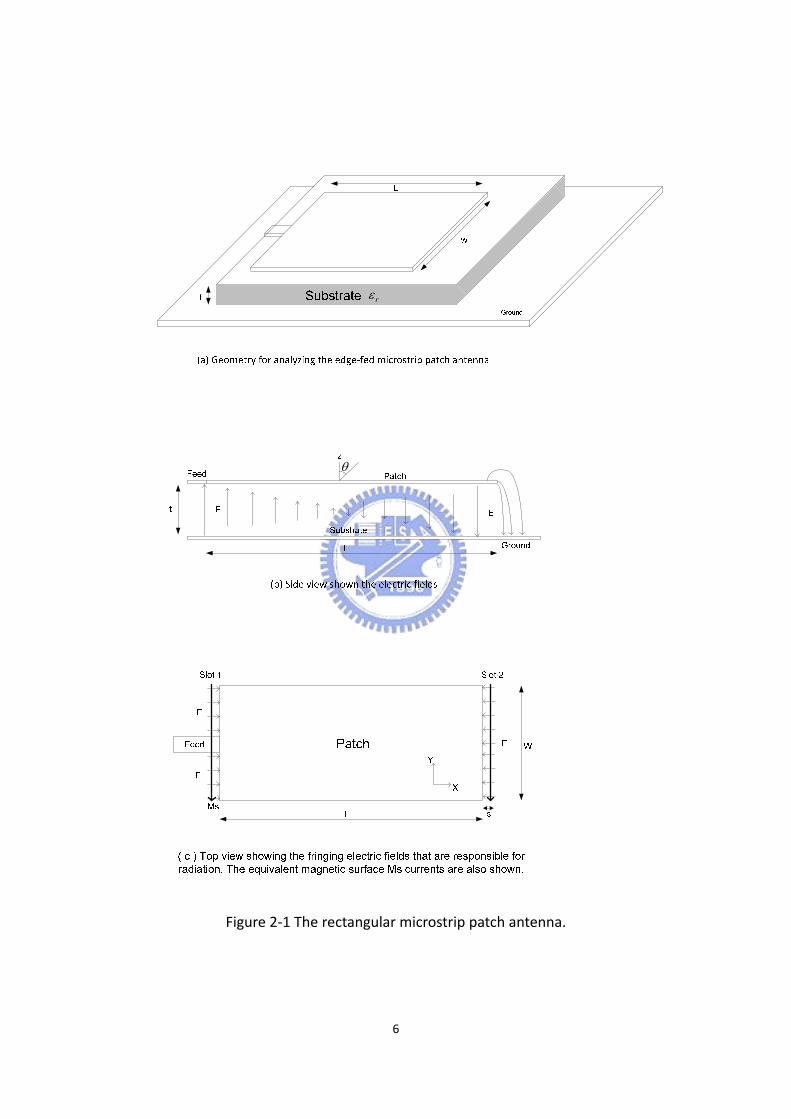
6
rε
θ
Figure 2‐1 The rectangular microstrip patch antenna
7
Techniques for feeding patches are summarized in Fig 2‐2 They can be classified
into three groups directly coupled electromagnetically coupled or aperture coupled
The direct coaxial probe feed illustrated in Fig 2‐2‐(a) is simple to implement by
extending the center conductor of the connector attached to the ground plane up to
the patch Impedance can be adjusted by proper placement of the probe feed The
probe feed with a gap in Fig 2‐2‐(d) has the advantages of coaxial feeds Also the
gap capacitance partially cancels the probe inductance permitting thicker substrates
xpΔ
Figure 2‐2 Techniques for feeding microstrip patch antennas
8
Bandwidth is often ultimate limiting performance parameter and can be found
from the following simple empirical formula for impedance bandwidth [9]
λεε t
LWBW
r
r2
1773
minus= 1ltlt
λt
(2‐5)
The bandwidth and efficiency of a patch are increased by increasing substrate
thickness t and by lowering rε
The inherently narrow impedance bandwidth is the major drawback of a
microstrip patch antenna Techniques for bandwidth enhancement have been
intensively studied in past decades Several methods including the utilization of
parasitic patch [10] thick substrates [11] and capacitively‐coupled feeding have been
suggested in literature The stacked geometry resulting from the addition of parasitic
patches will enlarge the size and increase the complexity in array fabrication which is
especially inconvenient for the coplanar case [12]
To broaden the bandwidth in rectangular patch antenna structure the
capacitively‐coupled feeding method is often chosen as the feeding topology
Recently in Fig 2‐3 a feeding approach employing an L‐shaped probe has been
proposed [13] It is already known that the L‐probe has been applied successfully in
other antenna designs [14] The L‐shaped probe is an excellent feed for patch
antennas with a thick substrate (thicknessasymp01 0λ ) The L‐probe incorporated with
the radiating patch introduces a capacitance suppressing some of the inductance
introduced by the probe itself With the use of a rectangular patch fed by the
Lndashprobe [15] the bandwidth and average gain can reach 35 and 75dBi
respectively
9
Figure 2‐3 Patch antenna fed by L‐shaped probe
22 Polarization
The perspective view of a certain polarized wave shows at a fixed instant of time
and the time sequence of electric field vectors as the wave passes through a fixed
plane There are some important special cases of the polarization ellipse If the
electric field vector moves back and forth along a line it is said to be linearly
polarized as shown in Fig 2‐4a If the electric field vector remains constant in length
but rotates around in a circular path it is circular polarized Rotation at radian
frequency ω is in one of two directions referred to as the sense of rotation If the
wave is traveling toward the observer and the vector rotates clockwise it is left‐hand
10
polarized If it rotates counterclockwise it is right‐hand polarized
Figure 2‐4 Some wave polarization states
In Fig 2‐5a shows a left‐hand circular‐polarization wave as the vector pattern
translates along the +Z‐axis the electric field at a fixed point appears to rotate
clockwise in the xy‐plane We can define the axial ratio (AR) as the major axis electric
field component to that along the minor axis of the polarization ellipse in Fig 2‐5
The sign of AR is positive for right‐hand sense and negative for left‐hand sense In Fig
2‐5 the electric field for wave can be express as
$ $ ( )( ) ( )j j t z
x yE x y z t x E y E e eφ ϖ βminus= +ur
(2‐6)
In Equation (2‐6) if the components are in‐phase (φ=0) the net vector is linearly
polarized If Ex=0 or Ey=0 vertical or horizontal linear polarization is produced
respectively If Ex= Ey andφ=plusmn90 deg the electromagnetic wave is left‐hand or
right‐hand circular polarization with +90deg or ‐ 90deg phase difference respectively as
shown in Fig 2‐5a and Fig 2‐5b
11
1 0ang deg
1 90ang deg
1 90ang deg
1 0ang deg
Figure 2‐5 The traveling circular‐polarization wave
23 Polarization of an antenna
The commonly used antenna structure with certain polarization state is
microstrip patch antenna The polarization of an antenna is the polarization of the
wave radiated in a given direction by the antenna when transmitting The ideal
linear‐ polarization antenna can be product by inverted‐F antenna microstrip patch
antenna or monopole antenna The perfect linear polarization antenna will provide
linear polarization wave in one direction When the antenna operates in linear
polarization state the cross‐polarization pattern determines the performance On
the other hand the proper circular polarization antenna is radiating two orthogonal
linear polarized wave with equal power and 90deg phase difference The antenna
structure with various polarization states has been discussed and applied in literature
[16‐17]
12
Chapter 3 Dual‐band Branch Line Coupler with
Wideband Switching Circuit
In this chapter we will propose the even‐odd mode method to design the
dual‐band BLC and combine it with the wideband switching circuit The dual‐band
BLC provides two equal power signals with 90deg phase difference in two operating
bands With the wideband switching circuit we can easily control the output power
of the dual‐band BLC to either go through the circuit or be absorbed by 50‐Ohm
termination from 2 GHz to 6 GHz
31 The Theory of Dual‐band BLC
The dual‐band BLC can provide two signals with equal power and 90deg phase
difference in both operating bands and the method of analyzing the BLC operating in
two bands has been proposed in [5] They present the composite rightleft‐handed
(CRLH) transmission line (TL) which is the combination of an LH TL and an RH TL to
design the dual‐band BLC In Fig 3‐1 the equivalent T‐model of the LH TL and RH TL
exhibit phase lead and phase lag respectively These attributes are applied to the
design of a dual‐band λ4 TL The CRLH‐TL is manipulated to design electrical
lengths plusmn90deg at two arbitrary frequencies using this concept
Figure 3‐1 T‐model of artificial RH and LH TL respectively
13
In [5] they series two (RH) right‐hand TLs and LH (left‐hand) two order T‐model
circuits to design the circuit with 90deg phase shift in two operating bands respectively
and through the telegrapher equations they also take C
LZOLsdot
=2 into account to
calculate the solution set L (inductor) and C (capacitor) in LH T‐model circuits and PR
(length of the RH TLs) The design flow of the dual‐band BLC have been suggested in
[5] via providing a solution set of L and C values and PR of the dual‐band BLC at two
fixed operating frequencies Utilizing the designed flow proposed in [5] to design a
BLC operated in WiFi and WiMAX applications the solution set of C L and PR of the
dual‐band BLC we get are 153pF 192nH 27mm in the 50‐Ohm branches and
219pF 134nH 27mm in the 35‐Ohm branches Then we found the solution sets we
got can not operate properly in lower WiFi band To solve the problem and explain
this phenomenon the different method of the even‐odd mode analysis method is
utilized in this chapter so that we can also get a solution set L C and PR of the
dual‐band BLC operated in WiFi and WiMAX applications The even‐mode and
odd‐mode circuits are shown in Fig 3‐2 including the circuit schematic of the
equivalent type and the practical type for solving the L and C values and PR of the
50‐Ohm branch The odd‐mode ABCD matrix of the equivalent circuit shown in Fig
3‐2(a) can be formed by multiplying the three matrices of each cascading
component and written as
⎥⎦
⎤⎢⎣
⎡minus⎥
⎦
⎤⎢⎣
⎡⎥⎦
⎤⎢⎣
⎡minus
=⎥⎦
⎤⎢⎣
⎡
minus101
101
11jdc
bajDC
BA
oFodd
(3-1)
⎥⎦
⎤⎢⎣
⎡⎥⎦
⎤⎢⎣
⎡⎥⎦
⎤⎢⎣
⎡=⎥
⎦
⎤⎢⎣
⎡
minus101
101
12jdc
bajDC
BA
oFodd
(3-2)
where +90deg phase difference ( 43 PP angminusang ) is in the first band (F1) and ‐90deg phase
difference ( 43 PP angminusang ) is in the second band (F2) respectively By multiplying the three
matrices of each cascading component in the practical circuit in Fig 3‐2(b) we can get
14
⎥⎦
⎤⎢⎣
⎡⎥⎦
⎤⎢⎣
⎡⎥⎦
⎤⎢⎣
⎡=⎥
⎦
⎤⎢⎣
⎡
minus101
101
1111
oooFodd Ydcba
YDCBA
(3-3)
⎥⎦
⎤⎢⎣
⎡⎥⎦
⎤⎢⎣
⎡⎥⎦
⎤⎢⎣
⎡=⎥
⎦
⎤⎢⎣
⎡
minus101
101
2222
oooFodd Ydcba
YDCBA
(3-4)
where the definition of the C in ABCD matrix is IV and itrsquos can be considered as the
admittance of Yo And the Yo1 and Yo2 are obtained in F1 and F2 operation respectively
)tan(]1[12)tan(]12[]1[
501505021501505050
21
5015050215050
21501500
1ROR
RRo PCLCZCL
PCLCLCZjY
βωωωβωωω
minus+minusminus+minus
=
(3-5)
)tan(]1[12)tan(]12[]1[
502505022502505050
22
5025050225050
2250250
2ROR
RORo PCLCZCL
PCLCLCZjYβωωωβωωω
minus+minusminus+minus
=
(3-6)
And ω C L PR and ZOR is the operating frequency capacitance inductor and the
length of RH TL and characteristic of RH TL impedance respectively while the
subscript 50 is the 50‐Ohm branch After comparing the formulations resulting from
the equivalent circuit and the practical circuit Equation (3‐3) and (3‐4) should be
equal to Equation (3‐1) and (3‐2) and we can therefore get
j
PCLCZCLPCLCLCZ
jRR
RR minus=minus+minus
minus+minus)tan(]1[12)tan(]12[]1[
5015050215015005050
21
5015050215050
21501500
βωωωβωωω
(3-7)
j
PCLCZCLPCLCLCZ
jRR
RR =minus+minus
minus+minus)tan(]1[12)tan(]12[]1[
5025050225025005050
22
5025050225050
22502500
βωωωβωωω
(3-8)
In the same manner the even‐mode ABCD matrix in the form of equivalent circuit
can be written by multiplying the three matrices of each cascading component as
⎥⎦
⎤⎢⎣
⎡⎥⎦
⎤⎢⎣
⎡⎥⎦
⎤⎢⎣
⎡=⎥
⎦
⎤⎢⎣
⎡
minus101
101
11jdc
bajDC
BA
eFeven (3-9)
⎥⎦
⎤⎢⎣
⎡minus⎥
⎦
⎤⎢⎣
⎡⎥⎦
⎤⎢⎣
⎡minus
=⎥⎦
⎤⎢⎣
⎡
minus101
101
22jdc
bajDC
BA
eFeven (3-10)
Similarly the even‐mode ABCD matrix in the form of the practical circuit shown in
15
Fig 3‐2(b) can be written as
⎥⎦
⎤⎢⎣
⎡⎥⎦
⎤⎢⎣
⎡⎥⎦
⎤⎢⎣
⎡=⎥
⎦
⎤⎢⎣
⎡
minus101
101
1111
eeeFeven Ydcba
YDCBA
(3-11)
⎥⎦
⎤⎢⎣
⎡⎥⎦
⎤⎢⎣
⎡⎥⎦
⎤⎢⎣
⎡=⎥
⎦
⎤⎢⎣
⎡
minus101
101
2222
eeeFeven Ydcba
YDCBA
(3-12)
where
)tan(1)tan()tan(
50150150050502
1
50150150502
15015001
RR
RRRe PCZCL
PPCLCZjYβωω
ββωω+minus
minus+minus=
(3-13)
)tan(1)tan()tan(
502502500505022
502502505022502500
2RR
RRRe PCZCL
PPCLCZjYβωω
ββωω+minus
minus+minus=
(3-14)
and the Ye1 and Ye2 is obtained in F1 and F2 operation respectively We can therefore
get another two equations from Equation (3‐9) to Equation (3‐14) as
j
PCZCLPPCLCZ
jRR
RRR =+minus
minus+minus
)tan(1)tan()tan(
50150150050502
1
50150150502
1501500
βωωββωω
(3-15)
j
PCZCLPPCLCZ
jRR
RRR minus=+minus
minus+minus)tan(1
)tan()tan(
502502500505022
502502505022502500
βωωββωω
(3-16)
(a)
16
(b)
Figure 3‐2 The even‐mode and odd‐mode circuit (a) Equivalent circuit (b) Practical circuit
Directly solving exact values of the three variables (C50 L50 and PL50) from
Equation (3‐7) (3‐8) (3‐15) and (3‐16) the solution set of C50 L50 and PL50 of the
dual‐band BLC we get are 159pF 264nH and 247mm in the 50‐Ohm branches The
same analysis sequence can be applied to find the solution set of C35 L35 and PL35 and
we got 228pF 185nH and 247mm in 35‐Ohm branches To exactly describe the
properties of the T‐model circuit the ABCD matrix of the T‐model circuit must equal
to the ABCD matrix of the transmission line with phase shift Lθ and characteristic
impedance ZOT so that we can got
22
12CC
LZOT ωminus=
(3-17)
⎟⎟⎠
⎞⎜⎜⎝
⎛
minusminussdot
=LC
LCL 2
2
112arctan
ωωθ
(3-18)
In equation (3‐17) the ZOT is depend on operating frequency and the 22
1Cω
term
can be neglected in high frequency and the value of ZOT affected by the 22
1Cω
term
17
seriously in low frequency Thus the C
LZOLsdot
=2 derived by telegrapher equation in
[5] can describe the circuit in high frequency but not in low frequency
In Fig 3‐3 a testing circuit schematic is setting to observe the properties of the
two order T‐model circuits solved by the method proposed in [5] and the even‐odd
mode method proposed in this chapter individually and verify the circuits designed
by two different analysis methods can absolutely work or not In Fig 3‐3 one of the
ports of the two‐order T‐model circuits is connects to a termination ZOR and we
observe the return loss at the other port of the testing circuit In Fig 3‐4 the ST1
curve is referring to the return loss of the testing circuit in which the L50 and C50 are
obtained by the design flow proposed in [5] and ST2 curve is referring to the return
loss of the testing circuit in which the L50 and C50 are solved by our even‐odd mode
analysis method At 245GHz the ST1 is about ‐67dB which is larger than ‐10dB and
the ST2 is about ‐74dB The smaller the dB value of the return loss is the two order
T‐model circuits can further considered as a transmission line with phase shift Lθ
and characteristic impedance ZOT (ZOT is very close to ZOR in two operating
frequencies) So the solution set of the L C and PR in the dual‐band hybrid solved by
the designed flow proposed in [5] can not work well in lower WiFi band By
increasing the order of the T‐model circuit to three the return loss of the T‐model
circuit designed by the method proposed in [5] can be small than ‐10dB at 245GHz
as shown in Fig 3‐4 ST3 curve but we can just use the two order T‐model circuits to
achieve the same goal Because the L and C value of the lump‐elements are slightly
various with frequency we make some adjustment to let the dual‐band BLC work
properly at WiFi and WiMAX operations The practical C L and PR of the dual‐band
BLC are 15 pF 16 nH and 2155 mm in the 35‐Ohm branches and 12 pF 18 nH and
2155 mm in the 50‐Ohm branches as shown in Table 3‐1 Consequently through our
eve
the
sect
Ta
n‐odd mod
dual‐band
tion 33
O
F
able 3‐1 The
e method t
BLC can p
Observation Por
Fig
Figure 3‐4 Th
e DIMENSIO
P (mm
C(pF
L(nH
o design th
properly wo
C
rt
ure 3‐3 The
he simulate
ON AND LC
m)
)
)
18
e dual‐band
ork at both
C
L
C
e testing circ
ed return los
C VALUES WBLC
Zo = 35
215
15
16
d BLC with t
h operating
C C
L
cuit schema
ss of the tes
WE IMPLEM
ohm
5
5
6
two order T
g band as
ZOR
Termination
atic
sting circuit
ENT IN THE
Zo = 50ohm
215
12
18
T‐model circ
shown in
n
ts
DUAL‐BAN
m
cuits
next
ND
19
32 Design of Wideband Switching Circuit
An RF choke circuit is usually implemented in order to block the RF signals and
make the circuit operation correctly The conventional circuit of RF choke is shown in
Fig 3‐5a If the power is incident into RF port 1 because the quarter‐wavelength TL is
a narrow‐band element operating in single band and can be considered a very high
inductive impedance the power will not travel to DC port and be received at RF port
2 However the inductor must be kept in the high impedance state in the dual‐bands
we desire to block the RF signal and provide a path for DC bias As a result the circuit
of wideband RF choke is sketched as a solution in Fig 3‐5b As shown in Fig 3‐5b the
power is incident from the RF port1 and there is only little leaky power traveling to
DC port because of the high inductive impedance Ls Most power will therefore travel
to RF port 2 Based on this concept we design a wideband switching circuit as shown
in Fig 3‐6 By changing the state of pin diodes we can control the power travels to
either RF2 port or 50Ω termination As the D1 is at ldquoONrdquo state D2 is at ldquoOFFrdquo state
and the power incident from RF1 the power cannot travel to RF2 As the D1 is at
ldquoOFFrdquo state D2 is at ldquoONrdquo state and the power incident from RF1 most of the power
will travel to RF2 The final chosen values of capacitor inductor and resistor are 66nH
30pF and 50Ω respectively
20
Figure 3‐5 The schematic circuit of RF choke
Figure 3‐6 The schematic circuit of wideband switch
21
33 Simulation and Measurement Results
In this section we will combine the dual‐band BLC and the wideband switching
circuit The circuit schematic of the combination circuit is shown in Fig 3‐7 As the
power is incident from Port1 and wideband switching circuit (1) and circuit (2) in Fig
3‐7 is at ldquoThroughrdquo state and ldquoTerminationrdquo state only Port2 have output power As
the power is incident from Port1 and wideband switching circuit (1) and circuit (2)
are at ldquoThroughrdquo state the power at Port2 and Port3 is equal and the phase
difference between two ports is 90deg In Table 3‐2 we list four operating senses
resulting from the combination of the dual‐band BLC and wideband switching circuit
We utilized HFSS to simulate the dual‐band BLC and the simulated performances
of Case 2 and Case 4 in Table 3‐2 are shown In Fig 3‐8 and Fig 3‐9 From Fig 3‐8 and
Fig 3‐9 the power difference between two output ports of the BLC is 047 dB and
052 dB respectively in the center frequency of WiFi and WiMAX operation in Case 2
state Moreover the simulated angle difference between two output ports is 84 deg
and ‐86 deg in center frequency of WiFi and WiMAX operation in Case 2 state
respectively as shown in Fig3‐10
The measured performances of Case 2 and Case 4 in Table 3‐2 are shown In Fig
3‐11 and Fig 3‐12 In Fig 3‐11 and Fig 3‐12 we find the bandwidth and the two
equal‐power branches with 90deg phase difference of this circuit are good for WiFi and
WiMAX applications From Fig 3‐11 and Fig 3‐12 the power difference between two
output ports of the BLC is 069 dB and 077 dB respectively in the center frequency of
WiFi and WiMAX operation in Case 2 state Moreover the measured angle difference
between two output ports is 83 deg and ‐98 deg in center frequency of WiFi and
WiMAX operation in Case 2 state respectively as shown in Fig 3‐13 Because of the
value deviation of lumped elements and the soldering effect the experimental
22
results are slightly different from the simulation results Fortunately the measured
bandwidth in each operating band is about 200MHz so it is still feasible for covering
each of the required bandwidth From Fig 3‐8 to Fig 13 the two output power in
WiMAX operation are lower than the two output power in WiFi operation Itrsquos caused
by the wavelength in WiMAX operation is shorter than the wavelength in WiFi
operation so the discontinuity area is increased and may affect the performance in
WiMAX operation
Figure 3‐7 Combination of the dual‐band BLC and two wideband switching circuits
Table 3‐2 THE OPERATING SENSE OF FOUR STATES OF COMBINATION OF THE
DUAL‐BAND BLC AND TWO WIDEBAND SWITHCING CIRCUITS
Intput Switching circuit (1) Switching circuit (2) Output
Case 1 Port 1 Through Termination Port2
Case 2 Port 1 Through Through Port2 and Port3
Case 3 Port 4 Termination Through Port3
Case 4 Port 4 Through Through Port2 and Port3
Figure 3‐8 The sim
(a)
(b) W
mulated resu
23
WiFi opera
WiMAX oper
ults of the d
ation
ration
dual‐band BBLC in Case
2 state
Figurre 3‐9 The s
(a)
(b) W
simulated re
24
WiFi opera
WiMAX oper
esults of du
ation
ration
al band BLCC in Case 4 s
state
Figure 3‐10 The
(a)
(b) W
e simulated
25
WiFi opera
WiMAX oper
angle differ
ation
ration
rence of thee dual‐band
d BLC
Figure 3‐11 MMeasured sc
with two
(a)
(b) W
cattering pa
wideband s
26
WiFi opera
WiMAX ope
arameters o
switching ci
ation
ration
of combinat
rcuits in Ca
ion of the d
se 2 state
dual‐band BBLC
Figgure 3‐12 Measured s
with two
(a)
(b) W
scattering p
wideband s27
WiFi opera
WiMAX ope
parameters
switching ci
ation
ration
of combina
rcuits in Ca
tion of the
se 4 state
dual‐band BLC
28
(a) WiFi operation
(b) WiMAX operation
Figure 3‐13 The measured angle difference of the dual‐band BLC
29
Chapter 4 Dual‐band Patch Antenna
In this chapter we will propose a square patch antenna fed by two L‐shaped
probe with four slots The two L‐shaped probes can effectively reduce the coupling
effect between two ports Moreover the square patch with four slots can make the
structure of the antenna symmetric and provide dual‐band operation
41 Antenna Design
The structure of slot is often adopted in the antenna design for either dual‐band
excitation or bandwidth enhancement As shown in Fig 4‐1 [18] they propose a
structure which consists of a rectangular patch loaded by two slots which are etched
close to the radiating edges where the bandwidth is about 2 in two operating
bands In this structure the slots are used to change the current of the TM30 mode
on the rectangular patch and make the current distribution become more similar
with the current distribution of TM10 and the current distribution in both operating
band are shown in Fig 4‐2 However because the patch is of the rectangular shape
it is hard to integrate two orthogonal linear polarization modes in a single patch
Moreover two directly‐fed coaxial probes in a single patch may cause serious
coupling as well
We therefore propose a square patch antenna fed by the L‐shaped probe with
four slots as shown in Fig 4‐3 The two slots along the X‐direction are parallel to the
X‐direction current distribution on the square patch so they will only disturb the
X‐direction current distribution slightly Because it is a symmetric structure we can
therefore utilize two L‐shaped probes feeding in orthogonal directions This
technique allows one square patch to set up two L‐shaped probes along X and Y
direction for producing two linear polarizations in a single patch and will not cause
30
serious coupling effect as well The geometric size of AH AG Lp Pw SL SG Sw we
implemented is 3mm 05mm 125mm 47mm 325mm 2mm and 06mm
respectively
Figure 4‐1 The probe‐fed patch antenna with a pair of slots
(a) (b) Figure 4‐2 The current distribution of the probe‐fed patch antenna with a pair of slots
(a) Lower band (b) Higher band
31
Figure 4‐3 Patch antenna fed by L‐shaped probe with four slots
42 Simulation and Measurement Results
The simulation and measurement results are shown in Fig 4‐4 The performance
of low S21 means coupling effect between two ports can be observed in both of the
desired frequency bands The simulated E‐plane radiation pattern at 245GHz and
35GHz are shown in Fig 4‐5 Because the magnitude of cross‐polarization pattern is
lower ‐10 dB it can be a good antenna candidate of linear polarization
Fig 4‐6 shows the measured radiation patterns The low cross polarization
represents that the additional two X‐direction slots only affect the X‐direction
current slightly The measured bandwidth and maximum gain are 244 and 923 dBi
at 245GHz respectively On the other hand the measured bandwidth and maximum
FR4 Substrate FR4 Substrate
Air
Feeding Line
Ground
Rectangular Patch
Ground
Feeding LineRectangular Patch
L-shaped probe
FR4 Substrate
FR4 Substrate
(a) Side view of L-shaped probe fed patch antenna
(b) Top view of L-shaped probe fed patch antenna with four slots
Slot
Slot
Slot
Slot
X
Y
Pw
SL
Lp
AH
AG
SwSG
gain
diffe
size
reas
n are 257
erent from
of the L‐s
sons make t
(a) T
(b) T
and 87 d
the simulat
haped prob
the patch m
The simulat
The measur
Bi at 35GH
ted results
bes and the
may not be f
ion result o
red result o32
z respectiv
It may be m
e gap betw
fabricated in
of the dual‐b
f the dual‐b
vely The me
mainly beca
ween the L‐
n the symm
band anten
band antenn
easured res
use of the d
‐shaped pro
metric mann
na in WiFi b
na in WiFi b
sults are slig
deviation of
obe The ab
er
band
band
ghtly
f the
bove
(c) Th
(d) Th
Figure 4‐4
he simulatio
he measure
The scatter
on result of
ed result of t
ring parame
two ortho
33
the dual‐ba
the dual‐ba
eters of the
ogonal L‐sh
and antenna
and antenna
patch ante
haped probe
a in WiMAX
a in WiMAX
enna with fo
es
X band
X band
our slots fedd by
34
-20 -15 -10 -5 0 5 10
45
-135
90
-90
135
-45
180 0
-20 -15 -10 -5 0 5 10
45
-135
90
-90
135
-45
180 0
(a) The simulated E‐plane radiation pattern at 245GHz
(b) The simulated E‐plane radiation pattern at 35GHz
Figure 4‐5 The simulated patterns of the patch antenna with four slots fed by two
orthogonal L‐shaped probes
Linear Polarization E‐plane-Co‐ -Cross
Linear Polarization E‐plane-Co‐ -Cross
35
-20 -15 -10 -5 0 5 10
45
-135
90
-90
135
-45
180 0
-20 -15 -10 -5 0 5 10
45
-135
90
-90
135
-45
180 0
(a) The measured E‐plane radiation pattern at 245GHz
(b) The measured E‐plane radiation pattern at 35GHz
Figure 4‐6 The measured patterns of the patch antenna with four slots fed by two
orthogonal L‐shaped probes
Linear Polarization E‐plane-Co‐ -Cross
Linear Polarization E‐plane-Co‐ -Cross
36
Chapter 5 The Dual‐band Reconfigurable
Quadri‐Polarization Diversity Antenna
We further combine the three parts (dual‐band BLC wideband switching circuit
and dual‐band patch antenna) which we have designed in the previous chapters and
present its performances The system block is shown in Fig 5‐1 As the wideband
switching circuit 1 and switching circuit 2 operate at ldquoThroughrdquo and ldquoTerminationrdquo
state respectively and the power is incident from port 1 the antenna can generate an
X‐directional linear polarization sense As the wideband switching circuit 1 and
switching circuit 2 both operate at ldquoThroughrdquo state and the power is incident from
port 1 the antenna can generate a left‐hand circular polarization sense in WiFi
operation In the same manner where the power is incidence from port4 the
antenna can generate a right‐hand circular polarization sense in WiFi operation The
operating modes of the proposed antenna are shown in Table 5‐1 From Table 5‐1
we find as the wideband switching circuits change their states the antenna structure
can provide quadri‐polarization in both operating bands
51 Simulation and Measurement Results
The top view of the whole simulated antenna structure in HFSS is shown in Fig
5‐2 The simulated scattering parameters in Case 1 (port 1 excitation) and Case 3
(port 2 excitation) state are shown in Fig 5‐3 and simulated scattering parameters of
Case 2 (port 1 excitation) and Case 4 (port 4 excitation) state are shown in Fig 5‐4
From the simulated scattering parameters we know the whole antenna structure is
feasible for covering each of the required bandwidth The simulated radiation
patterns of Case 1 are shown in Fig 5‐5 The simulated maximum gain in case 1 state
37
is 27dBi in WiFi and 22dBi in WiMAX operation respectively From the simulation
results since the cross‐polarization pattern is very small compared to the
co‐polarization pattern the antenna is convinced to have good operation in either
linear polarization or circular polarization
Figure 5‐1 The system block of the dual‐band antenna structure
38
Table 5‐1 STATUTES OF THE DUAL‐BAND ANTENNA STRUCTURE
Input Switching circuit (1) Switching circuit (2) Polarization sense
Case 1 Port 1 Through Termination X-direction
Linear Polarization
Case 2 Port 1 Through Through LHCP (WiFi operation)
RHCP (WiAX operation)
Case 3 Port 4 Termination Through Y-direction
Linear Polarization
Case 4 Port 4 Through Through RHCP (WiFi operation)
LHCP (WiAX operation)
The photograph of the antenna structure is shown in Fig 5‐6 The measured
performances of scattering parameters are shown in Fig 5‐7 and Fig 5‐8 and the
bandwidth is 57 and 6 in WiFi and WiMAX operation respectively The measured
radiation patterns are shown in Fig 5‐9 to Fig 5‐13 In Fig 5‐9 and Fig 5‐10 since
the cross‐polarization pattern is very small compared to the co‐polarization pattern
the dual‐band antenna is good for operating in linear polarization In Fig 5‐11a the
maximum gain is 25dBi and the 2‐dB axial‐ratio beamwidth is 86deg at 245GHz in Case
2 In Fig 5‐11b we can observe the maximum gain is about 19dBi and the 2‐dB
axial‐ratio beamwidth is 78deg at 35GHz in Case 2 The measured performances of the
dual‐band structure are listed in Table 5‐2 In Table5‐2 the quadri‐polarization
beamwidth means the axial‐ratio of LHCP and RHCP are lower than 2dB and the
magnitude of cross polarization of LP in Case 1 and Case 3 are lower than ‐10dB in
this beamwidth in each operating band
The measured maximum gain of Case 2 is little larger than the measured
maximum gain of Case 4 by 03dBi in 245GHz and 024dBi in 35GHz as shown in
Table 5‐2 To explain this phenomenon we must survey the power actually radiated
39
by the dual‐band patch antenna Therefore we have to get the scattering parameters
of the dual‐band patch antenna and dual‐band BLC individually In Section 3‐3 we
have got the simulated and measured scattering parameters of S21 and S31 which
can be considered A1 and A2 respectively the power incident to two L‐shaped probes
of the dual‐band patch antenna In Section 4‐2 we had simulated and measured
scattering parameters of the dual‐band patch antenna which can be considered a set
of SANT And the reflected power at Px and Py in Fig 5‐1 can be obtained by the
following equation
[ ] ⎥⎦
⎤⎢⎣
⎡sdot⎥
⎦
⎤⎢⎣
⎡=⎥
⎦
⎤⎢⎣
⎡sdot=⎥
⎦
⎤⎢⎣
⎡
2
1
2212
2111
2
1
2
1
AA
SSSS
AA
Sbb
ANT (5‐1)
where b1 and b2 is the quantity of reflected power at Px and Py respectively
Therefore the normalized power actually radiated by the dual‐band patch antenna is
2
22
12
22
1 bbAAP
PPi
ANTiANTi minusminus+== (5‐2)
where the Pi is the input power at port 1 or port 4 and the ANTiP is the power
actually radiated by the dual‐band patch antenna We first discuss the simulated
results of ANTiP In simulated results we get the parameters of A1 A2 and SANT and
substitute them into Equation (5‐2) We can therefore obtain b1 and b2 and the
normalized power ( ANTiP ) actually radiated by the dual‐band patch antenna is 0686
and 0685 in Case 2 and Case 4 state respectively in 245GHz In the same manner
we can get the normalized power ( ANTiP ) actually radiated by the dual‐band patch
antenna is 0554 and 0548 in Case 2 and Case 4 state respectively in 35GHz From
the computation results in both frequency bands because 1) the antenna structure is
symmetric 2) the lumped elements in HFSS are lossless and 3) the values of lumped
element donrsquot vary with frequency the power radiated by the dual‐band patch
antenna is almost equal in both of the two circular polarization states
40
Different from the simulated ones the measured A1 A2 and SANT can be gotten
from the previous chapter 3 and chapter 4 and we can use the same analysis
sequence to find the solutions of ANTiP The normalized power ( ANTiP ) actually
radiated by the dual‐band patch antenna is 0508 and 0403 in Case 2 and Case 4
state respectively in 245GHz and the normalized power ( ANTiP ) actually radiated by
the dual‐band patch antenna is 0462 and 0448 in Case 2 and Case 4 state
respectively in 35GHz Obviously the measured result ANTiP is lower than the
simulated result of ANTiP and itrsquos caused by the practical lumped elements provide
extra power loss Moreover the measured result of ANTiP in Case 4 is lower than the
measured result of ANTiP in Case 2 The calculated difference between Case 2 and
Case 4 is 006 in 245GHz and 008 in 35GHz so the measured maximum gain in Fig
5‐11 is slightly larger than the measured maximum gain in Fig 5‐12 by 022dBi in
245GHz and 024dBi in 35GHz The main reason of the imbalance may be that A1
and A2 of Case 2 is a little different from those of Case 4 at both frequency bands so
the actual radiated power of Case 2 and Case 4 will not be the same and result in the
asymmetric pattern gain at both frequency bands
Figure 5‐2 The top view of simulated antenna structure in HFSS
Figure 5‐33 The simul
(a)
(b) W
lated scatte
41
WiFi opera
WiMAX ope
ering param
ation
ration
eters in Casse 1 and Cas
se 3 state
Figure 5‐44 The simul
(a)
(b) W
lated scatte
42
WiFi opera
WiMAX ope
ering param
ation
ration
eters in Casse 2 and Cas
se 4 state
43
-20 -15 -10 -5 0 5
45
-135
90
-90
135
-45
180 0
-20 -15 -10 -5 0 5
45
-135
90
-90
135
-45
180 0
(a) 245GHz
(b) 35GHz
Figure 5‐5 The simulated radiation patterns in Case 1
Linear Polarization E‐plane-Co‐ -Cross
Linear Polarization E‐plane-Co‐ -Cross
44
(a) (b)
Figure 5‐6 The photographs of the dual‐band quadri‐polarization diversity patch
antenna (a) Front side of the structure (b) Back side of the structure
Figgure 5‐7 Thee measured
(a)
(b) W
d scattering
45
WiFi opera
WiMAX ope
parameters
and Case 3
ation
ration
s of the ant
enna struct
ture for Case 1
Figgure 5‐8 Thee measured
(a)
(b) W
d scattering
46
WiFi opera
WiMAX ope
parameters
and Case 4
ation
ration
s of the ant
enna struct
ture for Case 2
47
-20 -15 -10 -5 0 5
45
-135
90
-90
135
-45
180 0
-20 -15 -10 -5 0 5
45
-135
90
-90
135
-45
180 0
(a) The measured E‐plane radiation pattern at 245GHz
(b) The measured E‐plane radiation pattern at 35GHz
Figure 5‐9 The measured E‐plane radiation patterns in Case 1 state
Linear Polarization E‐plane-Co‐ -Cross
Linear Polarization E‐plane-Co‐ -Cross
48
-20 -15 -10 -5 0 5
45
-135
90
-90
135
-45
180 0
-20 -15 -10 -5 0 5
45
-135
90
-90
135
-45
180 0
(a) The measured E‐plane radiation pattern at 245GHz
(b) The measured E‐plane radiation pattern at 35GHz
Figure 5‐10 The measured E‐plane radiation patterns in Case 3 state
Linear Polarization E‐plane-Co‐ -Cross
Linear Polarization E‐plane-Co‐ -Cross
49
-20 -15 -10 -5 0 5
45
-135
90
-90
135
-45
180 0
-20 -15 -10 -5 0 5
45
-135
90
-90
135
-45
180 0
(a) Measured circular polarization radiation pattern at 245GHz
(b) Measured circular polarization radiation pattern at 35GHz
Figure 5‐11 The measured radiation patterns in Case 2 state
Circular Polarization- Gain
Circular Polarization- Gain
50
-20 -15 -10 -5 0 5
45
-135
90
-90
135
-45
180 0
-20 -15 -10 -5 0 5
45
-135
90
-90
135
-45
180 0
(a) Measured circular polarization radiation pattern at 245GHz
(b) Measured circular polarization radiation pattern at 35GHz
Figure 5‐12 The measured radiation patterns in Case 4 state
Circular Polarization- Gain
Circular Polarization- Gain
51
(a) 245GHz
(b) 35GHz
Figure 5‐13 The measured axial‐ratio of the proposed antenna
52
Table 5‐2 THE MEASURED PERFORMANCES OF THE DUAL‐BAND ANTENNA
STRUCTURE
Frequency Polarization
Sense
Axial Ratio lt 2
Beamwidth (Deg)
Quadri‐Polarization
Beamwidth (Deg)
Maxinum Gain
(dBi)
245GHz
RHCP (Case 4) 65
65
218 LHCP (Case 2) 90 24 LP (Case 1) XXX 23 LP (Case 3) XXX 2
35GHz
RHCP (Case 2) 95
70
18 LHCP (Case 4) 80 156 LP (Case 1) XXX 176 LP (Case 3) XXX 163
53
Chapter 6 Conclusion
We have provided another even‐odd mode method to design the dual‐band BLC
and combined it with the wideband switching circuits successfully in Chapter 3 With
the wideband switching circuit we can easily control the power to either go through
the circuit or be absorbed by 50‐Ohm termination from 2 GHz to 6 GHz The
dual‐band BLC provides two equal power signals with 90deg phase difference in two
operating bands In Chapter 4 a dual‐band patch antenna with low cross polarization
and coupling has been completely fabricated Because of the symmetry of the
antenna structure we proposed two L‐shaped probes can be easily integrated in a
single patch and the four additional slots are etched close to each radiation side to
produce another radiation frequency Finally we combine the above three parts to
fabricate a single patch antenna structure with dual‐band reconfigurable
quadri‐polarization diversity The measured results in Chapter 5 have shown our
proposed dual‐band quadric‐polarization diversity antenna meets our expectation
WiFi and WiMAX systems are becoming more popular in wireless communication
applications And one antenna structure operating in these two bands is becoming
more important Our antenna design can be one of the best solutions for enhancing
the communication quality The idea we present in this thesis is good but there is still
room for improvement to reach better performance First we may design a better
switching circuit to increase the antenna gain and reduce the lump elements
Moreover the design of the dual‐band quadri‐polarization diversity antenna is
convinced a rising topic and we provide one as a milestone for this demand We
believe the design of dual‐band quadri‐polarization diversity antenna will greatly
bring contribution to the communication technology
54
References
[1] 吳逸凡「新型可塑性四極化天線設計」國立交通大學碩士論文民國94
年
[2] 吳俊賢「可塑性四極化掃描天線之設計」國立交通大學碩士論文民國
95年
[3] W L Stutzman and G A Thiele Antenna Theory and Design 2nd ed New York
Wiley p 212‐215 1998
[4] C L Mak K M Luk K F Lee and Y L Chow ldquoExperimental Study of a Microstrip
Patch Antenna with an L‐shaped Proberdquo IEEE Trans Antenna amp Propagation vol
48 pp777‐783 May 2000
[5] I‐Hsiang Lin Marc DeVincentis Christophe Caloz and Tatsuo Itoh ldquoArbitrary
Dual‐Band Components Using Composite RightLeft ‐Handed Transmission Linesrdquo
IEEE Trans Microwave Theory and Techniques vol 52 pp 1142‐1149 Apr 2004
[6] K R Carver and J W Mink ldquoMicrostrip Antenna Technologyrdquo IEEE Trans
Antenna amp Propagation vol AP‐29 pp 2‐24 Jan 1981
[7] D H Schaubert ldquoMicrostrip Antennardquo Electromagnetics vol 12 pp 381‐401
July‐ December 1992
[8] R E Munson ldquoConformal Microstrip Antennas and Microstrip Phased Arraysrdquo
IEEE Trans Antennas amp Propagation vol AP‐22 pp74‐78 Jan 1974
[9] D R Jackson and N G Alexopoulos ldquoSimple Approximate Formulas for Input
Resistance Bandwidth and Efficiency of a Resonant Rectangular Patchrdquo IEEE
Trans Antennas amp Propagation vol 3 pp407‐410 Mar 1991
[10] R Q Lee K F Lee and J Bobinchak ldquoCharacteristics of a two‐layer
electromagnetically coupled rectangular patch antennardquo Electron Lett vol 23
pp 1070ndash1072 Sep 1987
55
[11] E Chang S A Long and W F Richards ldquoExperimental investigation of electrically
thick rectangular microstrip antennasrdquo IEEE Trans Antennas amp Propagation vol
AP‐43 pp 767ndash772 Jun 1986
[12] T M Au K F Tong and K M Luk ldquoCharacteristics of aperture‐coupled co‐planar
microstrip subarraysrdquo Inst Elect Eng Proc Microwave Antennas Propagat vol
144 pp 137ndash140 Apr 1997
[13] K M Luk C L Mak Y L Chow and K F Lee ldquoBroadband microstrip patch
antennardquo Electron Lett vol 34 pp 1442ndash1443 Jul 1998
[14] H Nakano M Yamazaki and J Yamauchi ldquoElectromagnetically coupled curl
antennardquo Electron Lett vol 33 pp 1003ndash1004 Jun 1997
[15] H Nakano M Yamazaki and J Yamauchi ldquoElectromagnetically coupled curl
antennardquo Electron Lett vol 33 pp 1003ndash1004 Jun 1997
[16] David M Pozar and Sean M Duffy ldquoA Dual‐Band Circular Polarized
Aperture‐Coupled Stacked Microstrip Antenna for Global Positioning Satelliterdquo
IEEE Trans Antennas amp Propagation vol 45 pp 1618‐1625 Nov 1997
[17] Stephen D Targonski and David M Pozar ldquoDesign of Wideband Circular
Polarized Aperture‐Coupled Microstrip Antennasrdquo IEEE Trans Antennas amp
Propagation vol 41 pp 214‐219 Feb 1993
[18] S Maci G B Gentili and G Avitabile ldquoSingle‐layer dual frequency patch
antennardquo Electron Lett vol 29 pp 1441‐1443 Aug 1993
- 封面pdf
- 羅馬pdf
- 內文_1-11_pdf
- 內文_12-28__paper版本_pdf
- 內文_29-35_pdf
- 內文_36-50_pdf
- 內文_51-52_pdf
- 內文_53-55_pdf
-
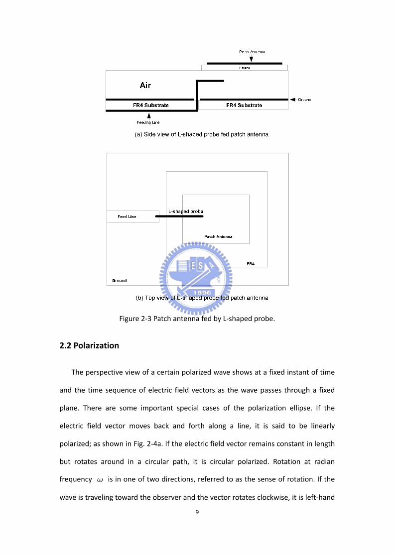

12
Chapter 3 Dual‐band Branch Line Coupler with
Wideband Switching Circuit
In this chapter we will propose the even‐odd mode method to design the
dual‐band BLC and combine it with the wideband switching circuit The dual‐band
BLC provides two equal power signals with 90deg phase difference in two operating
bands With the wideband switching circuit we can easily control the output power
of the dual‐band BLC to either go through the circuit or be absorbed by 50‐Ohm
termination from 2 GHz to 6 GHz
31 The Theory of Dual‐band BLC
The dual‐band BLC can provide two signals with equal power and 90deg phase
difference in both operating bands and the method of analyzing the BLC operating in
two bands has been proposed in [5] They present the composite rightleft‐handed
(CRLH) transmission line (TL) which is the combination of an LH TL and an RH TL to
design the dual‐band BLC In Fig 3‐1 the equivalent T‐model of the LH TL and RH TL
exhibit phase lead and phase lag respectively These attributes are applied to the
design of a dual‐band λ4 TL The CRLH‐TL is manipulated to design electrical
lengths plusmn90deg at two arbitrary frequencies using this concept
Figure 3‐1 T‐model of artificial RH and LH TL respectively
13
In [5] they series two (RH) right‐hand TLs and LH (left‐hand) two order T‐model
circuits to design the circuit with 90deg phase shift in two operating bands respectively
and through the telegrapher equations they also take C
LZOLsdot
=2 into account to
calculate the solution set L (inductor) and C (capacitor) in LH T‐model circuits and PR
(length of the RH TLs) The design flow of the dual‐band BLC have been suggested in
[5] via providing a solution set of L and C values and PR of the dual‐band BLC at two
fixed operating frequencies Utilizing the designed flow proposed in [5] to design a
BLC operated in WiFi and WiMAX applications the solution set of C L and PR of the
dual‐band BLC we get are 153pF 192nH 27mm in the 50‐Ohm branches and
219pF 134nH 27mm in the 35‐Ohm branches Then we found the solution sets we
got can not operate properly in lower WiFi band To solve the problem and explain
this phenomenon the different method of the even‐odd mode analysis method is
utilized in this chapter so that we can also get a solution set L C and PR of the
dual‐band BLC operated in WiFi and WiMAX applications The even‐mode and
odd‐mode circuits are shown in Fig 3‐2 including the circuit schematic of the
equivalent type and the practical type for solving the L and C values and PR of the
50‐Ohm branch The odd‐mode ABCD matrix of the equivalent circuit shown in Fig
3‐2(a) can be formed by multiplying the three matrices of each cascading
component and written as
⎥⎦
⎤⎢⎣
⎡minus⎥
⎦
⎤⎢⎣
⎡⎥⎦
⎤⎢⎣
⎡minus
=⎥⎦
⎤⎢⎣
⎡
minus101
101
11jdc
bajDC
BA
oFodd
(3-1)
⎥⎦
⎤⎢⎣
⎡⎥⎦
⎤⎢⎣
⎡⎥⎦
⎤⎢⎣
⎡=⎥
⎦
⎤⎢⎣
⎡
minus101
101
12jdc
bajDC
BA
oFodd
(3-2)
where +90deg phase difference ( 43 PP angminusang ) is in the first band (F1) and ‐90deg phase
difference ( 43 PP angminusang ) is in the second band (F2) respectively By multiplying the three
matrices of each cascading component in the practical circuit in Fig 3‐2(b) we can get
14
⎥⎦
⎤⎢⎣
⎡⎥⎦
⎤⎢⎣
⎡⎥⎦
⎤⎢⎣
⎡=⎥
⎦
⎤⎢⎣
⎡
minus101
101
1111
oooFodd Ydcba
YDCBA
(3-3)
⎥⎦
⎤⎢⎣
⎡⎥⎦
⎤⎢⎣
⎡⎥⎦
⎤⎢⎣
⎡=⎥
⎦
⎤⎢⎣
⎡
minus101
101
2222
oooFodd Ydcba
YDCBA
(3-4)
where the definition of the C in ABCD matrix is IV and itrsquos can be considered as the
admittance of Yo And the Yo1 and Yo2 are obtained in F1 and F2 operation respectively
)tan(]1[12)tan(]12[]1[
501505021501505050
21
5015050215050
21501500
1ROR
RRo PCLCZCL
PCLCLCZjY
βωωωβωωω
minus+minusminus+minus
=
(3-5)
)tan(]1[12)tan(]12[]1[
502505022502505050
22
5025050225050
2250250
2ROR
RORo PCLCZCL
PCLCLCZjYβωωωβωωω
minus+minusminus+minus
=
(3-6)
And ω C L PR and ZOR is the operating frequency capacitance inductor and the
length of RH TL and characteristic of RH TL impedance respectively while the
subscript 50 is the 50‐Ohm branch After comparing the formulations resulting from
the equivalent circuit and the practical circuit Equation (3‐3) and (3‐4) should be
equal to Equation (3‐1) and (3‐2) and we can therefore get
j
PCLCZCLPCLCLCZ
jRR
RR minus=minus+minus
minus+minus)tan(]1[12)tan(]12[]1[
5015050215015005050
21
5015050215050
21501500
βωωωβωωω
(3-7)
j
PCLCZCLPCLCLCZ
jRR
RR =minus+minus
minus+minus)tan(]1[12)tan(]12[]1[
5025050225025005050
22
5025050225050
22502500
βωωωβωωω
(3-8)
In the same manner the even‐mode ABCD matrix in the form of equivalent circuit
can be written by multiplying the three matrices of each cascading component as
⎥⎦
⎤⎢⎣
⎡⎥⎦
⎤⎢⎣
⎡⎥⎦
⎤⎢⎣
⎡=⎥
⎦
⎤⎢⎣
⎡
minus101
101
11jdc
bajDC
BA
eFeven (3-9)
⎥⎦
⎤⎢⎣
⎡minus⎥
⎦
⎤⎢⎣
⎡⎥⎦
⎤⎢⎣
⎡minus
=⎥⎦
⎤⎢⎣
⎡
minus101
101
22jdc
bajDC
BA
eFeven (3-10)
Similarly the even‐mode ABCD matrix in the form of the practical circuit shown in
15
Fig 3‐2(b) can be written as
⎥⎦
⎤⎢⎣
⎡⎥⎦
⎤⎢⎣
⎡⎥⎦
⎤⎢⎣
⎡=⎥
⎦
⎤⎢⎣
⎡
minus101
101
1111
eeeFeven Ydcba
YDCBA
(3-11)
⎥⎦
⎤⎢⎣
⎡⎥⎦
⎤⎢⎣
⎡⎥⎦
⎤⎢⎣
⎡=⎥
⎦
⎤⎢⎣
⎡
minus101
101
2222
eeeFeven Ydcba
YDCBA
(3-12)
where
)tan(1)tan()tan(
50150150050502
1
50150150502
15015001
RR
RRRe PCZCL
PPCLCZjYβωω
ββωω+minus
minus+minus=
(3-13)
)tan(1)tan()tan(
502502500505022
502502505022502500
2RR
RRRe PCZCL
PPCLCZjYβωω
ββωω+minus
minus+minus=
(3-14)
and the Ye1 and Ye2 is obtained in F1 and F2 operation respectively We can therefore
get another two equations from Equation (3‐9) to Equation (3‐14) as
j
PCZCLPPCLCZ
jRR
RRR =+minus
minus+minus
)tan(1)tan()tan(
50150150050502
1
50150150502
1501500
βωωββωω
(3-15)
j
PCZCLPPCLCZ
jRR
RRR minus=+minus
minus+minus)tan(1
)tan()tan(
502502500505022
502502505022502500
βωωββωω
(3-16)
(a)
16
(b)
Figure 3‐2 The even‐mode and odd‐mode circuit (a) Equivalent circuit (b) Practical circuit
Directly solving exact values of the three variables (C50 L50 and PL50) from
Equation (3‐7) (3‐8) (3‐15) and (3‐16) the solution set of C50 L50 and PL50 of the
dual‐band BLC we get are 159pF 264nH and 247mm in the 50‐Ohm branches The
same analysis sequence can be applied to find the solution set of C35 L35 and PL35 and
we got 228pF 185nH and 247mm in 35‐Ohm branches To exactly describe the
properties of the T‐model circuit the ABCD matrix of the T‐model circuit must equal
to the ABCD matrix of the transmission line with phase shift Lθ and characteristic
impedance ZOT so that we can got
22
12CC
LZOT ωminus=
(3-17)
⎟⎟⎠
⎞⎜⎜⎝
⎛
minusminussdot
=LC
LCL 2
2
112arctan
ωωθ
(3-18)
In equation (3‐17) the ZOT is depend on operating frequency and the 22
1Cω
term
can be neglected in high frequency and the value of ZOT affected by the 22
1Cω
term
17
seriously in low frequency Thus the C
LZOLsdot
=2 derived by telegrapher equation in
[5] can describe the circuit in high frequency but not in low frequency
In Fig 3‐3 a testing circuit schematic is setting to observe the properties of the
two order T‐model circuits solved by the method proposed in [5] and the even‐odd
mode method proposed in this chapter individually and verify the circuits designed
by two different analysis methods can absolutely work or not In Fig 3‐3 one of the
ports of the two‐order T‐model circuits is connects to a termination ZOR and we
observe the return loss at the other port of the testing circuit In Fig 3‐4 the ST1
curve is referring to the return loss of the testing circuit in which the L50 and C50 are
obtained by the design flow proposed in [5] and ST2 curve is referring to the return
loss of the testing circuit in which the L50 and C50 are solved by our even‐odd mode
analysis method At 245GHz the ST1 is about ‐67dB which is larger than ‐10dB and
the ST2 is about ‐74dB The smaller the dB value of the return loss is the two order
T‐model circuits can further considered as a transmission line with phase shift Lθ
and characteristic impedance ZOT (ZOT is very close to ZOR in two operating
frequencies) So the solution set of the L C and PR in the dual‐band hybrid solved by
the designed flow proposed in [5] can not work well in lower WiFi band By
increasing the order of the T‐model circuit to three the return loss of the T‐model
circuit designed by the method proposed in [5] can be small than ‐10dB at 245GHz
as shown in Fig 3‐4 ST3 curve but we can just use the two order T‐model circuits to
achieve the same goal Because the L and C value of the lump‐elements are slightly
various with frequency we make some adjustment to let the dual‐band BLC work
properly at WiFi and WiMAX operations The practical C L and PR of the dual‐band
BLC are 15 pF 16 nH and 2155 mm in the 35‐Ohm branches and 12 pF 18 nH and
2155 mm in the 50‐Ohm branches as shown in Table 3‐1 Consequently through our
eve
the
sect
Ta
n‐odd mod
dual‐band
tion 33
O
F
able 3‐1 The
e method t
BLC can p
Observation Por
Fig
Figure 3‐4 Th
e DIMENSIO
P (mm
C(pF
L(nH
o design th
properly wo
C
rt
ure 3‐3 The
he simulate
ON AND LC
m)
)
)
18
e dual‐band
ork at both
C
L
C
e testing circ
ed return los
C VALUES WBLC
Zo = 35
215
15
16
d BLC with t
h operating
C C
L
cuit schema
ss of the tes
WE IMPLEM
ohm
5
5
6
two order T
g band as
ZOR
Termination
atic
sting circuit
ENT IN THE
Zo = 50ohm
215
12
18
T‐model circ
shown in
n
ts
DUAL‐BAN
m
cuits
next
ND
19
32 Design of Wideband Switching Circuit
An RF choke circuit is usually implemented in order to block the RF signals and
make the circuit operation correctly The conventional circuit of RF choke is shown in
Fig 3‐5a If the power is incident into RF port 1 because the quarter‐wavelength TL is
a narrow‐band element operating in single band and can be considered a very high
inductive impedance the power will not travel to DC port and be received at RF port
2 However the inductor must be kept in the high impedance state in the dual‐bands
we desire to block the RF signal and provide a path for DC bias As a result the circuit
of wideband RF choke is sketched as a solution in Fig 3‐5b As shown in Fig 3‐5b the
power is incident from the RF port1 and there is only little leaky power traveling to
DC port because of the high inductive impedance Ls Most power will therefore travel
to RF port 2 Based on this concept we design a wideband switching circuit as shown
in Fig 3‐6 By changing the state of pin diodes we can control the power travels to
either RF2 port or 50Ω termination As the D1 is at ldquoONrdquo state D2 is at ldquoOFFrdquo state
and the power incident from RF1 the power cannot travel to RF2 As the D1 is at
ldquoOFFrdquo state D2 is at ldquoONrdquo state and the power incident from RF1 most of the power
will travel to RF2 The final chosen values of capacitor inductor and resistor are 66nH
30pF and 50Ω respectively
20
Figure 3‐5 The schematic circuit of RF choke
Figure 3‐6 The schematic circuit of wideband switch
21
33 Simulation and Measurement Results
In this section we will combine the dual‐band BLC and the wideband switching
circuit The circuit schematic of the combination circuit is shown in Fig 3‐7 As the
power is incident from Port1 and wideband switching circuit (1) and circuit (2) in Fig
3‐7 is at ldquoThroughrdquo state and ldquoTerminationrdquo state only Port2 have output power As
the power is incident from Port1 and wideband switching circuit (1) and circuit (2)
are at ldquoThroughrdquo state the power at Port2 and Port3 is equal and the phase
difference between two ports is 90deg In Table 3‐2 we list four operating senses
resulting from the combination of the dual‐band BLC and wideband switching circuit
We utilized HFSS to simulate the dual‐band BLC and the simulated performances
of Case 2 and Case 4 in Table 3‐2 are shown In Fig 3‐8 and Fig 3‐9 From Fig 3‐8 and
Fig 3‐9 the power difference between two output ports of the BLC is 047 dB and
052 dB respectively in the center frequency of WiFi and WiMAX operation in Case 2
state Moreover the simulated angle difference between two output ports is 84 deg
and ‐86 deg in center frequency of WiFi and WiMAX operation in Case 2 state
respectively as shown in Fig3‐10
The measured performances of Case 2 and Case 4 in Table 3‐2 are shown In Fig
3‐11 and Fig 3‐12 In Fig 3‐11 and Fig 3‐12 we find the bandwidth and the two
equal‐power branches with 90deg phase difference of this circuit are good for WiFi and
WiMAX applications From Fig 3‐11 and Fig 3‐12 the power difference between two
output ports of the BLC is 069 dB and 077 dB respectively in the center frequency of
WiFi and WiMAX operation in Case 2 state Moreover the measured angle difference
between two output ports is 83 deg and ‐98 deg in center frequency of WiFi and
WiMAX operation in Case 2 state respectively as shown in Fig 3‐13 Because of the
value deviation of lumped elements and the soldering effect the experimental
22
results are slightly different from the simulation results Fortunately the measured
bandwidth in each operating band is about 200MHz so it is still feasible for covering
each of the required bandwidth From Fig 3‐8 to Fig 13 the two output power in
WiMAX operation are lower than the two output power in WiFi operation Itrsquos caused
by the wavelength in WiMAX operation is shorter than the wavelength in WiFi
operation so the discontinuity area is increased and may affect the performance in
WiMAX operation
Figure 3‐7 Combination of the dual‐band BLC and two wideband switching circuits
Table 3‐2 THE OPERATING SENSE OF FOUR STATES OF COMBINATION OF THE
DUAL‐BAND BLC AND TWO WIDEBAND SWITHCING CIRCUITS
Intput Switching circuit (1) Switching circuit (2) Output
Case 1 Port 1 Through Termination Port2
Case 2 Port 1 Through Through Port2 and Port3
Case 3 Port 4 Termination Through Port3
Case 4 Port 4 Through Through Port2 and Port3
Figure 3‐8 The sim
(a)
(b) W
mulated resu
23
WiFi opera
WiMAX oper
ults of the d
ation
ration
dual‐band BBLC in Case
2 state
Figurre 3‐9 The s
(a)
(b) W
simulated re
24
WiFi opera
WiMAX oper
esults of du
ation
ration
al band BLCC in Case 4 s
state
Figure 3‐10 The
(a)
(b) W
e simulated
25
WiFi opera
WiMAX oper
angle differ
ation
ration
rence of thee dual‐band
d BLC
Figure 3‐11 MMeasured sc
with two
(a)
(b) W
cattering pa
wideband s
26
WiFi opera
WiMAX ope
arameters o
switching ci
ation
ration
of combinat
rcuits in Ca
ion of the d
se 2 state
dual‐band BBLC
Figgure 3‐12 Measured s
with two
(a)
(b) W
scattering p
wideband s27
WiFi opera
WiMAX ope
parameters
switching ci
ation
ration
of combina
rcuits in Ca
tion of the
se 4 state
dual‐band BLC
28
(a) WiFi operation
(b) WiMAX operation
Figure 3‐13 The measured angle difference of the dual‐band BLC
29
Chapter 4 Dual‐band Patch Antenna
In this chapter we will propose a square patch antenna fed by two L‐shaped
probe with four slots The two L‐shaped probes can effectively reduce the coupling
effect between two ports Moreover the square patch with four slots can make the
structure of the antenna symmetric and provide dual‐band operation
41 Antenna Design
The structure of slot is often adopted in the antenna design for either dual‐band
excitation or bandwidth enhancement As shown in Fig 4‐1 [18] they propose a
structure which consists of a rectangular patch loaded by two slots which are etched
close to the radiating edges where the bandwidth is about 2 in two operating
bands In this structure the slots are used to change the current of the TM30 mode
on the rectangular patch and make the current distribution become more similar
with the current distribution of TM10 and the current distribution in both operating
band are shown in Fig 4‐2 However because the patch is of the rectangular shape
it is hard to integrate two orthogonal linear polarization modes in a single patch
Moreover two directly‐fed coaxial probes in a single patch may cause serious
coupling as well
We therefore propose a square patch antenna fed by the L‐shaped probe with
four slots as shown in Fig 4‐3 The two slots along the X‐direction are parallel to the
X‐direction current distribution on the square patch so they will only disturb the
X‐direction current distribution slightly Because it is a symmetric structure we can
therefore utilize two L‐shaped probes feeding in orthogonal directions This
technique allows one square patch to set up two L‐shaped probes along X and Y
direction for producing two linear polarizations in a single patch and will not cause
30
serious coupling effect as well The geometric size of AH AG Lp Pw SL SG Sw we
implemented is 3mm 05mm 125mm 47mm 325mm 2mm and 06mm
respectively
Figure 4‐1 The probe‐fed patch antenna with a pair of slots
(a) (b) Figure 4‐2 The current distribution of the probe‐fed patch antenna with a pair of slots
(a) Lower band (b) Higher band
31
Figure 4‐3 Patch antenna fed by L‐shaped probe with four slots
42 Simulation and Measurement Results
The simulation and measurement results are shown in Fig 4‐4 The performance
of low S21 means coupling effect between two ports can be observed in both of the
desired frequency bands The simulated E‐plane radiation pattern at 245GHz and
35GHz are shown in Fig 4‐5 Because the magnitude of cross‐polarization pattern is
lower ‐10 dB it can be a good antenna candidate of linear polarization
Fig 4‐6 shows the measured radiation patterns The low cross polarization
represents that the additional two X‐direction slots only affect the X‐direction
current slightly The measured bandwidth and maximum gain are 244 and 923 dBi
at 245GHz respectively On the other hand the measured bandwidth and maximum
FR4 Substrate FR4 Substrate
Air
Feeding Line
Ground
Rectangular Patch
Ground
Feeding LineRectangular Patch
L-shaped probe
FR4 Substrate
FR4 Substrate
(a) Side view of L-shaped probe fed patch antenna
(b) Top view of L-shaped probe fed patch antenna with four slots
Slot
Slot
Slot
Slot
X
Y
Pw
SL
Lp
AH
AG
SwSG
gain
diffe
size
reas
n are 257
erent from
of the L‐s
sons make t
(a) T
(b) T
and 87 d
the simulat
haped prob
the patch m
The simulat
The measur
Bi at 35GH
ted results
bes and the
may not be f
ion result o
red result o32
z respectiv
It may be m
e gap betw
fabricated in
of the dual‐b
f the dual‐b
vely The me
mainly beca
ween the L‐
n the symm
band anten
band antenn
easured res
use of the d
‐shaped pro
metric mann
na in WiFi b
na in WiFi b
sults are slig
deviation of
obe The ab
er
band
band
ghtly
f the
bove
(c) Th
(d) Th
Figure 4‐4
he simulatio
he measure
The scatter
on result of
ed result of t
ring parame
two ortho
33
the dual‐ba
the dual‐ba
eters of the
ogonal L‐sh
and antenna
and antenna
patch ante
haped probe
a in WiMAX
a in WiMAX
enna with fo
es
X band
X band
our slots fedd by
34
-20 -15 -10 -5 0 5 10
45
-135
90
-90
135
-45
180 0
-20 -15 -10 -5 0 5 10
45
-135
90
-90
135
-45
180 0
(a) The simulated E‐plane radiation pattern at 245GHz
(b) The simulated E‐plane radiation pattern at 35GHz
Figure 4‐5 The simulated patterns of the patch antenna with four slots fed by two
orthogonal L‐shaped probes
Linear Polarization E‐plane-Co‐ -Cross
Linear Polarization E‐plane-Co‐ -Cross
35
-20 -15 -10 -5 0 5 10
45
-135
90
-90
135
-45
180 0
-20 -15 -10 -5 0 5 10
45
-135
90
-90
135
-45
180 0
(a) The measured E‐plane radiation pattern at 245GHz
(b) The measured E‐plane radiation pattern at 35GHz
Figure 4‐6 The measured patterns of the patch antenna with four slots fed by two
orthogonal L‐shaped probes
Linear Polarization E‐plane-Co‐ -Cross
Linear Polarization E‐plane-Co‐ -Cross
36
Chapter 5 The Dual‐band Reconfigurable
Quadri‐Polarization Diversity Antenna
We further combine the three parts (dual‐band BLC wideband switching circuit
and dual‐band patch antenna) which we have designed in the previous chapters and
present its performances The system block is shown in Fig 5‐1 As the wideband
switching circuit 1 and switching circuit 2 operate at ldquoThroughrdquo and ldquoTerminationrdquo
state respectively and the power is incident from port 1 the antenna can generate an
X‐directional linear polarization sense As the wideband switching circuit 1 and
switching circuit 2 both operate at ldquoThroughrdquo state and the power is incident from
port 1 the antenna can generate a left‐hand circular polarization sense in WiFi
operation In the same manner where the power is incidence from port4 the
antenna can generate a right‐hand circular polarization sense in WiFi operation The
operating modes of the proposed antenna are shown in Table 5‐1 From Table 5‐1
we find as the wideband switching circuits change their states the antenna structure
can provide quadri‐polarization in both operating bands
51 Simulation and Measurement Results
The top view of the whole simulated antenna structure in HFSS is shown in Fig
5‐2 The simulated scattering parameters in Case 1 (port 1 excitation) and Case 3
(port 2 excitation) state are shown in Fig 5‐3 and simulated scattering parameters of
Case 2 (port 1 excitation) and Case 4 (port 4 excitation) state are shown in Fig 5‐4
From the simulated scattering parameters we know the whole antenna structure is
feasible for covering each of the required bandwidth The simulated radiation
patterns of Case 1 are shown in Fig 5‐5 The simulated maximum gain in case 1 state
37
is 27dBi in WiFi and 22dBi in WiMAX operation respectively From the simulation
results since the cross‐polarization pattern is very small compared to the
co‐polarization pattern the antenna is convinced to have good operation in either
linear polarization or circular polarization
Figure 5‐1 The system block of the dual‐band antenna structure
38
Table 5‐1 STATUTES OF THE DUAL‐BAND ANTENNA STRUCTURE
Input Switching circuit (1) Switching circuit (2) Polarization sense
Case 1 Port 1 Through Termination X-direction
Linear Polarization
Case 2 Port 1 Through Through LHCP (WiFi operation)
RHCP (WiAX operation)
Case 3 Port 4 Termination Through Y-direction
Linear Polarization
Case 4 Port 4 Through Through RHCP (WiFi operation)
LHCP (WiAX operation)
The photograph of the antenna structure is shown in Fig 5‐6 The measured
performances of scattering parameters are shown in Fig 5‐7 and Fig 5‐8 and the
bandwidth is 57 and 6 in WiFi and WiMAX operation respectively The measured
radiation patterns are shown in Fig 5‐9 to Fig 5‐13 In Fig 5‐9 and Fig 5‐10 since
the cross‐polarization pattern is very small compared to the co‐polarization pattern
the dual‐band antenna is good for operating in linear polarization In Fig 5‐11a the
maximum gain is 25dBi and the 2‐dB axial‐ratio beamwidth is 86deg at 245GHz in Case
2 In Fig 5‐11b we can observe the maximum gain is about 19dBi and the 2‐dB
axial‐ratio beamwidth is 78deg at 35GHz in Case 2 The measured performances of the
dual‐band structure are listed in Table 5‐2 In Table5‐2 the quadri‐polarization
beamwidth means the axial‐ratio of LHCP and RHCP are lower than 2dB and the
magnitude of cross polarization of LP in Case 1 and Case 3 are lower than ‐10dB in
this beamwidth in each operating band
The measured maximum gain of Case 2 is little larger than the measured
maximum gain of Case 4 by 03dBi in 245GHz and 024dBi in 35GHz as shown in
Table 5‐2 To explain this phenomenon we must survey the power actually radiated
39
by the dual‐band patch antenna Therefore we have to get the scattering parameters
of the dual‐band patch antenna and dual‐band BLC individually In Section 3‐3 we
have got the simulated and measured scattering parameters of S21 and S31 which
can be considered A1 and A2 respectively the power incident to two L‐shaped probes
of the dual‐band patch antenna In Section 4‐2 we had simulated and measured
scattering parameters of the dual‐band patch antenna which can be considered a set
of SANT And the reflected power at Px and Py in Fig 5‐1 can be obtained by the
following equation
[ ] ⎥⎦
⎤⎢⎣
⎡sdot⎥
⎦
⎤⎢⎣
⎡=⎥
⎦
⎤⎢⎣
⎡sdot=⎥
⎦
⎤⎢⎣
⎡
2
1
2212
2111
2
1
2
1
AA
SSSS
AA
Sbb
ANT (5‐1)
where b1 and b2 is the quantity of reflected power at Px and Py respectively
Therefore the normalized power actually radiated by the dual‐band patch antenna is
2
22
12
22
1 bbAAP
PPi
ANTiANTi minusminus+== (5‐2)
where the Pi is the input power at port 1 or port 4 and the ANTiP is the power
actually radiated by the dual‐band patch antenna We first discuss the simulated
results of ANTiP In simulated results we get the parameters of A1 A2 and SANT and
substitute them into Equation (5‐2) We can therefore obtain b1 and b2 and the
normalized power ( ANTiP ) actually radiated by the dual‐band patch antenna is 0686
and 0685 in Case 2 and Case 4 state respectively in 245GHz In the same manner
we can get the normalized power ( ANTiP ) actually radiated by the dual‐band patch
antenna is 0554 and 0548 in Case 2 and Case 4 state respectively in 35GHz From
the computation results in both frequency bands because 1) the antenna structure is
symmetric 2) the lumped elements in HFSS are lossless and 3) the values of lumped
element donrsquot vary with frequency the power radiated by the dual‐band patch
antenna is almost equal in both of the two circular polarization states
40
Different from the simulated ones the measured A1 A2 and SANT can be gotten
from the previous chapter 3 and chapter 4 and we can use the same analysis
sequence to find the solutions of ANTiP The normalized power ( ANTiP ) actually
radiated by the dual‐band patch antenna is 0508 and 0403 in Case 2 and Case 4
state respectively in 245GHz and the normalized power ( ANTiP ) actually radiated by
the dual‐band patch antenna is 0462 and 0448 in Case 2 and Case 4 state
respectively in 35GHz Obviously the measured result ANTiP is lower than the
simulated result of ANTiP and itrsquos caused by the practical lumped elements provide
extra power loss Moreover the measured result of ANTiP in Case 4 is lower than the
measured result of ANTiP in Case 2 The calculated difference between Case 2 and
Case 4 is 006 in 245GHz and 008 in 35GHz so the measured maximum gain in Fig
5‐11 is slightly larger than the measured maximum gain in Fig 5‐12 by 022dBi in
245GHz and 024dBi in 35GHz The main reason of the imbalance may be that A1
and A2 of Case 2 is a little different from those of Case 4 at both frequency bands so
the actual radiated power of Case 2 and Case 4 will not be the same and result in the
asymmetric pattern gain at both frequency bands
Figure 5‐2 The top view of simulated antenna structure in HFSS
Figure 5‐33 The simul
(a)
(b) W
lated scatte
41
WiFi opera
WiMAX ope
ering param
ation
ration
eters in Casse 1 and Cas
se 3 state
Figure 5‐44 The simul
(a)
(b) W
lated scatte
42
WiFi opera
WiMAX ope
ering param
ation
ration
eters in Casse 2 and Cas
se 4 state
43
-20 -15 -10 -5 0 5
45
-135
90
-90
135
-45
180 0
-20 -15 -10 -5 0 5
45
-135
90
-90
135
-45
180 0
(a) 245GHz
(b) 35GHz
Figure 5‐5 The simulated radiation patterns in Case 1
Linear Polarization E‐plane-Co‐ -Cross
Linear Polarization E‐plane-Co‐ -Cross
44
(a) (b)
Figure 5‐6 The photographs of the dual‐band quadri‐polarization diversity patch
antenna (a) Front side of the structure (b) Back side of the structure
Figgure 5‐7 Thee measured
(a)
(b) W
d scattering
45
WiFi opera
WiMAX ope
parameters
and Case 3
ation
ration
s of the ant
enna struct
ture for Case 1
Figgure 5‐8 Thee measured
(a)
(b) W
d scattering
46
WiFi opera
WiMAX ope
parameters
and Case 4
ation
ration
s of the ant
enna struct
ture for Case 2
47
-20 -15 -10 -5 0 5
45
-135
90
-90
135
-45
180 0
-20 -15 -10 -5 0 5
45
-135
90
-90
135
-45
180 0
(a) The measured E‐plane radiation pattern at 245GHz
(b) The measured E‐plane radiation pattern at 35GHz
Figure 5‐9 The measured E‐plane radiation patterns in Case 1 state
Linear Polarization E‐plane-Co‐ -Cross
Linear Polarization E‐plane-Co‐ -Cross
48
-20 -15 -10 -5 0 5
45
-135
90
-90
135
-45
180 0
-20 -15 -10 -5 0 5
45
-135
90
-90
135
-45
180 0
(a) The measured E‐plane radiation pattern at 245GHz
(b) The measured E‐plane radiation pattern at 35GHz
Figure 5‐10 The measured E‐plane radiation patterns in Case 3 state
Linear Polarization E‐plane-Co‐ -Cross
Linear Polarization E‐plane-Co‐ -Cross
49
-20 -15 -10 -5 0 5
45
-135
90
-90
135
-45
180 0
-20 -15 -10 -5 0 5
45
-135
90
-90
135
-45
180 0
(a) Measured circular polarization radiation pattern at 245GHz
(b) Measured circular polarization radiation pattern at 35GHz
Figure 5‐11 The measured radiation patterns in Case 2 state
Circular Polarization- Gain
Circular Polarization- Gain
50
-20 -15 -10 -5 0 5
45
-135
90
-90
135
-45
180 0
-20 -15 -10 -5 0 5
45
-135
90
-90
135
-45
180 0
(a) Measured circular polarization radiation pattern at 245GHz
(b) Measured circular polarization radiation pattern at 35GHz
Figure 5‐12 The measured radiation patterns in Case 4 state
Circular Polarization- Gain
Circular Polarization- Gain
51
(a) 245GHz
(b) 35GHz
Figure 5‐13 The measured axial‐ratio of the proposed antenna
52
Table 5‐2 THE MEASURED PERFORMANCES OF THE DUAL‐BAND ANTENNA
STRUCTURE
Frequency Polarization
Sense
Axial Ratio lt 2
Beamwidth (Deg)
Quadri‐Polarization
Beamwidth (Deg)
Maxinum Gain
(dBi)
245GHz
RHCP (Case 4) 65
65
218 LHCP (Case 2) 90 24 LP (Case 1) XXX 23 LP (Case 3) XXX 2
35GHz
RHCP (Case 2) 95
70
18 LHCP (Case 4) 80 156 LP (Case 1) XXX 176 LP (Case 3) XXX 163
53
Chapter 6 Conclusion
We have provided another even‐odd mode method to design the dual‐band BLC
and combined it with the wideband switching circuits successfully in Chapter 3 With
the wideband switching circuit we can easily control the power to either go through
the circuit or be absorbed by 50‐Ohm termination from 2 GHz to 6 GHz The
dual‐band BLC provides two equal power signals with 90deg phase difference in two
operating bands In Chapter 4 a dual‐band patch antenna with low cross polarization
and coupling has been completely fabricated Because of the symmetry of the
antenna structure we proposed two L‐shaped probes can be easily integrated in a
single patch and the four additional slots are etched close to each radiation side to
produce another radiation frequency Finally we combine the above three parts to
fabricate a single patch antenna structure with dual‐band reconfigurable
quadri‐polarization diversity The measured results in Chapter 5 have shown our
proposed dual‐band quadric‐polarization diversity antenna meets our expectation
WiFi and WiMAX systems are becoming more popular in wireless communication
applications And one antenna structure operating in these two bands is becoming
more important Our antenna design can be one of the best solutions for enhancing
the communication quality The idea we present in this thesis is good but there is still
room for improvement to reach better performance First we may design a better
switching circuit to increase the antenna gain and reduce the lump elements
Moreover the design of the dual‐band quadri‐polarization diversity antenna is
convinced a rising topic and we provide one as a milestone for this demand We
believe the design of dual‐band quadri‐polarization diversity antenna will greatly
bring contribution to the communication technology
54
References
[1] 吳逸凡「新型可塑性四極化天線設計」國立交通大學碩士論文民國94
年
[2] 吳俊賢「可塑性四極化掃描天線之設計」國立交通大學碩士論文民國
95年
[3] W L Stutzman and G A Thiele Antenna Theory and Design 2nd ed New York
Wiley p 212‐215 1998
[4] C L Mak K M Luk K F Lee and Y L Chow ldquoExperimental Study of a Microstrip
Patch Antenna with an L‐shaped Proberdquo IEEE Trans Antenna amp Propagation vol
48 pp777‐783 May 2000
[5] I‐Hsiang Lin Marc DeVincentis Christophe Caloz and Tatsuo Itoh ldquoArbitrary
Dual‐Band Components Using Composite RightLeft ‐Handed Transmission Linesrdquo
IEEE Trans Microwave Theory and Techniques vol 52 pp 1142‐1149 Apr 2004
[6] K R Carver and J W Mink ldquoMicrostrip Antenna Technologyrdquo IEEE Trans
Antenna amp Propagation vol AP‐29 pp 2‐24 Jan 1981
[7] D H Schaubert ldquoMicrostrip Antennardquo Electromagnetics vol 12 pp 381‐401
July‐ December 1992
[8] R E Munson ldquoConformal Microstrip Antennas and Microstrip Phased Arraysrdquo
IEEE Trans Antennas amp Propagation vol AP‐22 pp74‐78 Jan 1974
[9] D R Jackson and N G Alexopoulos ldquoSimple Approximate Formulas for Input
Resistance Bandwidth and Efficiency of a Resonant Rectangular Patchrdquo IEEE
Trans Antennas amp Propagation vol 3 pp407‐410 Mar 1991
[10] R Q Lee K F Lee and J Bobinchak ldquoCharacteristics of a two‐layer
electromagnetically coupled rectangular patch antennardquo Electron Lett vol 23
pp 1070ndash1072 Sep 1987
55
[11] E Chang S A Long and W F Richards ldquoExperimental investigation of electrically
thick rectangular microstrip antennasrdquo IEEE Trans Antennas amp Propagation vol
AP‐43 pp 767ndash772 Jun 1986
[12] T M Au K F Tong and K M Luk ldquoCharacteristics of aperture‐coupled co‐planar
microstrip subarraysrdquo Inst Elect Eng Proc Microwave Antennas Propagat vol
144 pp 137ndash140 Apr 1997
[13] K M Luk C L Mak Y L Chow and K F Lee ldquoBroadband microstrip patch
antennardquo Electron Lett vol 34 pp 1442ndash1443 Jul 1998
[14] H Nakano M Yamazaki and J Yamauchi ldquoElectromagnetically coupled curl
antennardquo Electron Lett vol 33 pp 1003ndash1004 Jun 1997
[15] H Nakano M Yamazaki and J Yamauchi ldquoElectromagnetically coupled curl
antennardquo Electron Lett vol 33 pp 1003ndash1004 Jun 1997
[16] David M Pozar and Sean M Duffy ldquoA Dual‐Band Circular Polarized
Aperture‐Coupled Stacked Microstrip Antenna for Global Positioning Satelliterdquo
IEEE Trans Antennas amp Propagation vol 45 pp 1618‐1625 Nov 1997
[17] Stephen D Targonski and David M Pozar ldquoDesign of Wideband Circular
Polarized Aperture‐Coupled Microstrip Antennasrdquo IEEE Trans Antennas amp
Propagation vol 41 pp 214‐219 Feb 1993
[18] S Maci G B Gentili and G Avitabile ldquoSingle‐layer dual frequency patch
antennardquo Electron Lett vol 29 pp 1441‐1443 Aug 1993
- 封面pdf
- 羅馬pdf
- 內文_1-11_pdf
- 內文_12-28__paper版本_pdf
- 內文_29-35_pdf
- 內文_36-50_pdf
- 內文_51-52_pdf
- 內文_53-55_pdf
-

15
Fig 3‐2(b) can be written as
⎥⎦
⎤⎢⎣
⎡⎥⎦
⎤⎢⎣
⎡⎥⎦
⎤⎢⎣
⎡=⎥
⎦
⎤⎢⎣
⎡
minus101
101
1111
eeeFeven Ydcba
YDCBA
(3-11)
⎥⎦
⎤⎢⎣
⎡⎥⎦
⎤⎢⎣
⎡⎥⎦
⎤⎢⎣
⎡=⎥
⎦
⎤⎢⎣
⎡
minus101
101
2222
eeeFeven Ydcba
YDCBA
(3-12)
where
)tan(1)tan()tan(
50150150050502
1
50150150502
15015001
RR
RRRe PCZCL
PPCLCZjYβωω
ββωω+minus
minus+minus=
(3-13)
)tan(1)tan()tan(
502502500505022
502502505022502500
2RR
RRRe PCZCL
PPCLCZjYβωω
ββωω+minus
minus+minus=
(3-14)
and the Ye1 and Ye2 is obtained in F1 and F2 operation respectively We can therefore
get another two equations from Equation (3‐9) to Equation (3‐14) as
j
PCZCLPPCLCZ
jRR
RRR =+minus
minus+minus
)tan(1)tan()tan(
50150150050502
1
50150150502
1501500
βωωββωω
(3-15)
j
PCZCLPPCLCZ
jRR
RRR minus=+minus
minus+minus)tan(1
)tan()tan(
502502500505022
502502505022502500
βωωββωω
(3-16)
(a)
16
(b)
Figure 3‐2 The even‐mode and odd‐mode circuit (a) Equivalent circuit (b) Practical circuit
Directly solving exact values of the three variables (C50 L50 and PL50) from
Equation (3‐7) (3‐8) (3‐15) and (3‐16) the solution set of C50 L50 and PL50 of the
dual‐band BLC we get are 159pF 264nH and 247mm in the 50‐Ohm branches The
same analysis sequence can be applied to find the solution set of C35 L35 and PL35 and
we got 228pF 185nH and 247mm in 35‐Ohm branches To exactly describe the
properties of the T‐model circuit the ABCD matrix of the T‐model circuit must equal
to the ABCD matrix of the transmission line with phase shift Lθ and characteristic
impedance ZOT so that we can got
22
12CC
LZOT ωminus=
(3-17)
⎟⎟⎠
⎞⎜⎜⎝
⎛
minusminussdot
=LC
LCL 2
2
112arctan
ωωθ
(3-18)
In equation (3‐17) the ZOT is depend on operating frequency and the 22
1Cω
term
can be neglected in high frequency and the value of ZOT affected by the 22
1Cω
term
17
seriously in low frequency Thus the C
LZOLsdot
=2 derived by telegrapher equation in
[5] can describe the circuit in high frequency but not in low frequency
In Fig 3‐3 a testing circuit schematic is setting to observe the properties of the
two order T‐model circuits solved by the method proposed in [5] and the even‐odd
mode method proposed in this chapter individually and verify the circuits designed
by two different analysis methods can absolutely work or not In Fig 3‐3 one of the
ports of the two‐order T‐model circuits is connects to a termination ZOR and we
observe the return loss at the other port of the testing circuit In Fig 3‐4 the ST1
curve is referring to the return loss of the testing circuit in which the L50 and C50 are
obtained by the design flow proposed in [5] and ST2 curve is referring to the return
loss of the testing circuit in which the L50 and C50 are solved by our even‐odd mode
analysis method At 245GHz the ST1 is about ‐67dB which is larger than ‐10dB and
the ST2 is about ‐74dB The smaller the dB value of the return loss is the two order
T‐model circuits can further considered as a transmission line with phase shift Lθ
and characteristic impedance ZOT (ZOT is very close to ZOR in two operating
frequencies) So the solution set of the L C and PR in the dual‐band hybrid solved by
the designed flow proposed in [5] can not work well in lower WiFi band By
increasing the order of the T‐model circuit to three the return loss of the T‐model
circuit designed by the method proposed in [5] can be small than ‐10dB at 245GHz
as shown in Fig 3‐4 ST3 curve but we can just use the two order T‐model circuits to
achieve the same goal Because the L and C value of the lump‐elements are slightly
various with frequency we make some adjustment to let the dual‐band BLC work
properly at WiFi and WiMAX operations The practical C L and PR of the dual‐band
BLC are 15 pF 16 nH and 2155 mm in the 35‐Ohm branches and 12 pF 18 nH and
2155 mm in the 50‐Ohm branches as shown in Table 3‐1 Consequently through our
eve
the
sect
Ta
n‐odd mod
dual‐band
tion 33
O
F
able 3‐1 The
e method t
BLC can p
Observation Por
Fig
Figure 3‐4 Th
e DIMENSIO
P (mm
C(pF
L(nH
o design th
properly wo
C
rt
ure 3‐3 The
he simulate
ON AND LC
m)
)
)
18
e dual‐band
ork at both
C
L
C
e testing circ
ed return los
C VALUES WBLC
Zo = 35
215
15
16
d BLC with t
h operating
C C
L
cuit schema
ss of the tes
WE IMPLEM
ohm
5
5
6
two order T
g band as
ZOR
Termination
atic
sting circuit
ENT IN THE
Zo = 50ohm
215
12
18
T‐model circ
shown in
n
ts
DUAL‐BAN
m
cuits
next
ND
19
32 Design of Wideband Switching Circuit
An RF choke circuit is usually implemented in order to block the RF signals and
make the circuit operation correctly The conventional circuit of RF choke is shown in
Fig 3‐5a If the power is incident into RF port 1 because the quarter‐wavelength TL is
a narrow‐band element operating in single band and can be considered a very high
inductive impedance the power will not travel to DC port and be received at RF port
2 However the inductor must be kept in the high impedance state in the dual‐bands
we desire to block the RF signal and provide a path for DC bias As a result the circuit
of wideband RF choke is sketched as a solution in Fig 3‐5b As shown in Fig 3‐5b the
power is incident from the RF port1 and there is only little leaky power traveling to
DC port because of the high inductive impedance Ls Most power will therefore travel
to RF port 2 Based on this concept we design a wideband switching circuit as shown
in Fig 3‐6 By changing the state of pin diodes we can control the power travels to
either RF2 port or 50Ω termination As the D1 is at ldquoONrdquo state D2 is at ldquoOFFrdquo state
and the power incident from RF1 the power cannot travel to RF2 As the D1 is at
ldquoOFFrdquo state D2 is at ldquoONrdquo state and the power incident from RF1 most of the power
will travel to RF2 The final chosen values of capacitor inductor and resistor are 66nH
30pF and 50Ω respectively
20
Figure 3‐5 The schematic circuit of RF choke
Figure 3‐6 The schematic circuit of wideband switch
21
33 Simulation and Measurement Results
In this section we will combine the dual‐band BLC and the wideband switching
circuit The circuit schematic of the combination circuit is shown in Fig 3‐7 As the
power is incident from Port1 and wideband switching circuit (1) and circuit (2) in Fig
3‐7 is at ldquoThroughrdquo state and ldquoTerminationrdquo state only Port2 have output power As
the power is incident from Port1 and wideband switching circuit (1) and circuit (2)
are at ldquoThroughrdquo state the power at Port2 and Port3 is equal and the phase
difference between two ports is 90deg In Table 3‐2 we list four operating senses
resulting from the combination of the dual‐band BLC and wideband switching circuit
We utilized HFSS to simulate the dual‐band BLC and the simulated performances
of Case 2 and Case 4 in Table 3‐2 are shown In Fig 3‐8 and Fig 3‐9 From Fig 3‐8 and
Fig 3‐9 the power difference between two output ports of the BLC is 047 dB and
052 dB respectively in the center frequency of WiFi and WiMAX operation in Case 2
state Moreover the simulated angle difference between two output ports is 84 deg
and ‐86 deg in center frequency of WiFi and WiMAX operation in Case 2 state
respectively as shown in Fig3‐10
The measured performances of Case 2 and Case 4 in Table 3‐2 are shown In Fig
3‐11 and Fig 3‐12 In Fig 3‐11 and Fig 3‐12 we find the bandwidth and the two
equal‐power branches with 90deg phase difference of this circuit are good for WiFi and
WiMAX applications From Fig 3‐11 and Fig 3‐12 the power difference between two
output ports of the BLC is 069 dB and 077 dB respectively in the center frequency of
WiFi and WiMAX operation in Case 2 state Moreover the measured angle difference
between two output ports is 83 deg and ‐98 deg in center frequency of WiFi and
WiMAX operation in Case 2 state respectively as shown in Fig 3‐13 Because of the
value deviation of lumped elements and the soldering effect the experimental
22
results are slightly different from the simulation results Fortunately the measured
bandwidth in each operating band is about 200MHz so it is still feasible for covering
each of the required bandwidth From Fig 3‐8 to Fig 13 the two output power in
WiMAX operation are lower than the two output power in WiFi operation Itrsquos caused
by the wavelength in WiMAX operation is shorter than the wavelength in WiFi
operation so the discontinuity area is increased and may affect the performance in
WiMAX operation
Figure 3‐7 Combination of the dual‐band BLC and two wideband switching circuits
Table 3‐2 THE OPERATING SENSE OF FOUR STATES OF COMBINATION OF THE
DUAL‐BAND BLC AND TWO WIDEBAND SWITHCING CIRCUITS
Intput Switching circuit (1) Switching circuit (2) Output
Case 1 Port 1 Through Termination Port2
Case 2 Port 1 Through Through Port2 and Port3
Case 3 Port 4 Termination Through Port3
Case 4 Port 4 Through Through Port2 and Port3
Figure 3‐8 The sim
(a)
(b) W
mulated resu
23
WiFi opera
WiMAX oper
ults of the d
ation
ration
dual‐band BBLC in Case
2 state
Figurre 3‐9 The s
(a)
(b) W
simulated re
24
WiFi opera
WiMAX oper
esults of du
ation
ration
al band BLCC in Case 4 s
state
Figure 3‐10 The
(a)
(b) W
e simulated
25
WiFi opera
WiMAX oper
angle differ
ation
ration
rence of thee dual‐band
d BLC
Figure 3‐11 MMeasured sc
with two
(a)
(b) W
cattering pa
wideband s
26
WiFi opera
WiMAX ope
arameters o
switching ci
ation
ration
of combinat
rcuits in Ca
ion of the d
se 2 state
dual‐band BBLC
Figgure 3‐12 Measured s
with two
(a)
(b) W
scattering p
wideband s27
WiFi opera
WiMAX ope
parameters
switching ci
ation
ration
of combina
rcuits in Ca
tion of the
se 4 state
dual‐band BLC
28
(a) WiFi operation
(b) WiMAX operation
Figure 3‐13 The measured angle difference of the dual‐band BLC
29
Chapter 4 Dual‐band Patch Antenna
In this chapter we will propose a square patch antenna fed by two L‐shaped
probe with four slots The two L‐shaped probes can effectively reduce the coupling
effect between two ports Moreover the square patch with four slots can make the
structure of the antenna symmetric and provide dual‐band operation
41 Antenna Design
The structure of slot is often adopted in the antenna design for either dual‐band
excitation or bandwidth enhancement As shown in Fig 4‐1 [18] they propose a
structure which consists of a rectangular patch loaded by two slots which are etched
close to the radiating edges where the bandwidth is about 2 in two operating
bands In this structure the slots are used to change the current of the TM30 mode
on the rectangular patch and make the current distribution become more similar
with the current distribution of TM10 and the current distribution in both operating
band are shown in Fig 4‐2 However because the patch is of the rectangular shape
it is hard to integrate two orthogonal linear polarization modes in a single patch
Moreover two directly‐fed coaxial probes in a single patch may cause serious
coupling as well
We therefore propose a square patch antenna fed by the L‐shaped probe with
four slots as shown in Fig 4‐3 The two slots along the X‐direction are parallel to the
X‐direction current distribution on the square patch so they will only disturb the
X‐direction current distribution slightly Because it is a symmetric structure we can
therefore utilize two L‐shaped probes feeding in orthogonal directions This
technique allows one square patch to set up two L‐shaped probes along X and Y
direction for producing two linear polarizations in a single patch and will not cause
30
serious coupling effect as well The geometric size of AH AG Lp Pw SL SG Sw we
implemented is 3mm 05mm 125mm 47mm 325mm 2mm and 06mm
respectively
Figure 4‐1 The probe‐fed patch antenna with a pair of slots
(a) (b) Figure 4‐2 The current distribution of the probe‐fed patch antenna with a pair of slots
(a) Lower band (b) Higher band
31
Figure 4‐3 Patch antenna fed by L‐shaped probe with four slots
42 Simulation and Measurement Results
The simulation and measurement results are shown in Fig 4‐4 The performance
of low S21 means coupling effect between two ports can be observed in both of the
desired frequency bands The simulated E‐plane radiation pattern at 245GHz and
35GHz are shown in Fig 4‐5 Because the magnitude of cross‐polarization pattern is
lower ‐10 dB it can be a good antenna candidate of linear polarization
Fig 4‐6 shows the measured radiation patterns The low cross polarization
represents that the additional two X‐direction slots only affect the X‐direction
current slightly The measured bandwidth and maximum gain are 244 and 923 dBi
at 245GHz respectively On the other hand the measured bandwidth and maximum
FR4 Substrate FR4 Substrate
Air
Feeding Line
Ground
Rectangular Patch
Ground
Feeding LineRectangular Patch
L-shaped probe
FR4 Substrate
FR4 Substrate
(a) Side view of L-shaped probe fed patch antenna
(b) Top view of L-shaped probe fed patch antenna with four slots
Slot
Slot
Slot
Slot
X
Y
Pw
SL
Lp
AH
AG
SwSG
gain
diffe
size
reas
n are 257
erent from
of the L‐s
sons make t
(a) T
(b) T
and 87 d
the simulat
haped prob
the patch m
The simulat
The measur
Bi at 35GH
ted results
bes and the
may not be f
ion result o
red result o32
z respectiv
It may be m
e gap betw
fabricated in
of the dual‐b
f the dual‐b
vely The me
mainly beca
ween the L‐
n the symm
band anten
band antenn
easured res
use of the d
‐shaped pro
metric mann
na in WiFi b
na in WiFi b
sults are slig
deviation of
obe The ab
er
band
band
ghtly
f the
bove
(c) Th
(d) Th
Figure 4‐4
he simulatio
he measure
The scatter
on result of
ed result of t
ring parame
two ortho
33
the dual‐ba
the dual‐ba
eters of the
ogonal L‐sh
and antenna
and antenna
patch ante
haped probe
a in WiMAX
a in WiMAX
enna with fo
es
X band
X band
our slots fedd by
34
-20 -15 -10 -5 0 5 10
45
-135
90
-90
135
-45
180 0
-20 -15 -10 -5 0 5 10
45
-135
90
-90
135
-45
180 0
(a) The simulated E‐plane radiation pattern at 245GHz
(b) The simulated E‐plane radiation pattern at 35GHz
Figure 4‐5 The simulated patterns of the patch antenna with four slots fed by two
orthogonal L‐shaped probes
Linear Polarization E‐plane-Co‐ -Cross
Linear Polarization E‐plane-Co‐ -Cross
35
-20 -15 -10 -5 0 5 10
45
-135
90
-90
135
-45
180 0
-20 -15 -10 -5 0 5 10
45
-135
90
-90
135
-45
180 0
(a) The measured E‐plane radiation pattern at 245GHz
(b) The measured E‐plane radiation pattern at 35GHz
Figure 4‐6 The measured patterns of the patch antenna with four slots fed by two
orthogonal L‐shaped probes
Linear Polarization E‐plane-Co‐ -Cross
Linear Polarization E‐plane-Co‐ -Cross
36
Chapter 5 The Dual‐band Reconfigurable
Quadri‐Polarization Diversity Antenna
We further combine the three parts (dual‐band BLC wideband switching circuit
and dual‐band patch antenna) which we have designed in the previous chapters and
present its performances The system block is shown in Fig 5‐1 As the wideband
switching circuit 1 and switching circuit 2 operate at ldquoThroughrdquo and ldquoTerminationrdquo
state respectively and the power is incident from port 1 the antenna can generate an
X‐directional linear polarization sense As the wideband switching circuit 1 and
switching circuit 2 both operate at ldquoThroughrdquo state and the power is incident from
port 1 the antenna can generate a left‐hand circular polarization sense in WiFi
operation In the same manner where the power is incidence from port4 the
antenna can generate a right‐hand circular polarization sense in WiFi operation The
operating modes of the proposed antenna are shown in Table 5‐1 From Table 5‐1
we find as the wideband switching circuits change their states the antenna structure
can provide quadri‐polarization in both operating bands
51 Simulation and Measurement Results
The top view of the whole simulated antenna structure in HFSS is shown in Fig
5‐2 The simulated scattering parameters in Case 1 (port 1 excitation) and Case 3
(port 2 excitation) state are shown in Fig 5‐3 and simulated scattering parameters of
Case 2 (port 1 excitation) and Case 4 (port 4 excitation) state are shown in Fig 5‐4
From the simulated scattering parameters we know the whole antenna structure is
feasible for covering each of the required bandwidth The simulated radiation
patterns of Case 1 are shown in Fig 5‐5 The simulated maximum gain in case 1 state
37
is 27dBi in WiFi and 22dBi in WiMAX operation respectively From the simulation
results since the cross‐polarization pattern is very small compared to the
co‐polarization pattern the antenna is convinced to have good operation in either
linear polarization or circular polarization
Figure 5‐1 The system block of the dual‐band antenna structure
38
Table 5‐1 STATUTES OF THE DUAL‐BAND ANTENNA STRUCTURE
Input Switching circuit (1) Switching circuit (2) Polarization sense
Case 1 Port 1 Through Termination X-direction
Linear Polarization
Case 2 Port 1 Through Through LHCP (WiFi operation)
RHCP (WiAX operation)
Case 3 Port 4 Termination Through Y-direction
Linear Polarization
Case 4 Port 4 Through Through RHCP (WiFi operation)
LHCP (WiAX operation)
The photograph of the antenna structure is shown in Fig 5‐6 The measured
performances of scattering parameters are shown in Fig 5‐7 and Fig 5‐8 and the
bandwidth is 57 and 6 in WiFi and WiMAX operation respectively The measured
radiation patterns are shown in Fig 5‐9 to Fig 5‐13 In Fig 5‐9 and Fig 5‐10 since
the cross‐polarization pattern is very small compared to the co‐polarization pattern
the dual‐band antenna is good for operating in linear polarization In Fig 5‐11a the
maximum gain is 25dBi and the 2‐dB axial‐ratio beamwidth is 86deg at 245GHz in Case
2 In Fig 5‐11b we can observe the maximum gain is about 19dBi and the 2‐dB
axial‐ratio beamwidth is 78deg at 35GHz in Case 2 The measured performances of the
dual‐band structure are listed in Table 5‐2 In Table5‐2 the quadri‐polarization
beamwidth means the axial‐ratio of LHCP and RHCP are lower than 2dB and the
magnitude of cross polarization of LP in Case 1 and Case 3 are lower than ‐10dB in
this beamwidth in each operating band
The measured maximum gain of Case 2 is little larger than the measured
maximum gain of Case 4 by 03dBi in 245GHz and 024dBi in 35GHz as shown in
Table 5‐2 To explain this phenomenon we must survey the power actually radiated
39
by the dual‐band patch antenna Therefore we have to get the scattering parameters
of the dual‐band patch antenna and dual‐band BLC individually In Section 3‐3 we
have got the simulated and measured scattering parameters of S21 and S31 which
can be considered A1 and A2 respectively the power incident to two L‐shaped probes
of the dual‐band patch antenna In Section 4‐2 we had simulated and measured
scattering parameters of the dual‐band patch antenna which can be considered a set
of SANT And the reflected power at Px and Py in Fig 5‐1 can be obtained by the
following equation
[ ] ⎥⎦
⎤⎢⎣
⎡sdot⎥
⎦
⎤⎢⎣
⎡=⎥
⎦
⎤⎢⎣
⎡sdot=⎥
⎦
⎤⎢⎣
⎡
2
1
2212
2111
2
1
2
1
AA
SSSS
AA
Sbb
ANT (5‐1)
where b1 and b2 is the quantity of reflected power at Px and Py respectively
Therefore the normalized power actually radiated by the dual‐band patch antenna is
2
22
12
22
1 bbAAP
PPi
ANTiANTi minusminus+== (5‐2)
where the Pi is the input power at port 1 or port 4 and the ANTiP is the power
actually radiated by the dual‐band patch antenna We first discuss the simulated
results of ANTiP In simulated results we get the parameters of A1 A2 and SANT and
substitute them into Equation (5‐2) We can therefore obtain b1 and b2 and the
normalized power ( ANTiP ) actually radiated by the dual‐band patch antenna is 0686
and 0685 in Case 2 and Case 4 state respectively in 245GHz In the same manner
we can get the normalized power ( ANTiP ) actually radiated by the dual‐band patch
antenna is 0554 and 0548 in Case 2 and Case 4 state respectively in 35GHz From
the computation results in both frequency bands because 1) the antenna structure is
symmetric 2) the lumped elements in HFSS are lossless and 3) the values of lumped
element donrsquot vary with frequency the power radiated by the dual‐band patch
antenna is almost equal in both of the two circular polarization states
40
Different from the simulated ones the measured A1 A2 and SANT can be gotten
from the previous chapter 3 and chapter 4 and we can use the same analysis
sequence to find the solutions of ANTiP The normalized power ( ANTiP ) actually
radiated by the dual‐band patch antenna is 0508 and 0403 in Case 2 and Case 4
state respectively in 245GHz and the normalized power ( ANTiP ) actually radiated by
the dual‐band patch antenna is 0462 and 0448 in Case 2 and Case 4 state
respectively in 35GHz Obviously the measured result ANTiP is lower than the
simulated result of ANTiP and itrsquos caused by the practical lumped elements provide
extra power loss Moreover the measured result of ANTiP in Case 4 is lower than the
measured result of ANTiP in Case 2 The calculated difference between Case 2 and
Case 4 is 006 in 245GHz and 008 in 35GHz so the measured maximum gain in Fig
5‐11 is slightly larger than the measured maximum gain in Fig 5‐12 by 022dBi in
245GHz and 024dBi in 35GHz The main reason of the imbalance may be that A1
and A2 of Case 2 is a little different from those of Case 4 at both frequency bands so
the actual radiated power of Case 2 and Case 4 will not be the same and result in the
asymmetric pattern gain at both frequency bands
Figure 5‐2 The top view of simulated antenna structure in HFSS
Figure 5‐33 The simul
(a)
(b) W
lated scatte
41
WiFi opera
WiMAX ope
ering param
ation
ration
eters in Casse 1 and Cas
se 3 state
Figure 5‐44 The simul
(a)
(b) W
lated scatte
42
WiFi opera
WiMAX ope
ering param
ation
ration
eters in Casse 2 and Cas
se 4 state
43
-20 -15 -10 -5 0 5
45
-135
90
-90
135
-45
180 0
-20 -15 -10 -5 0 5
45
-135
90
-90
135
-45
180 0
(a) 245GHz
(b) 35GHz
Figure 5‐5 The simulated radiation patterns in Case 1
Linear Polarization E‐plane-Co‐ -Cross
Linear Polarization E‐plane-Co‐ -Cross
44
(a) (b)
Figure 5‐6 The photographs of the dual‐band quadri‐polarization diversity patch
antenna (a) Front side of the structure (b) Back side of the structure
Figgure 5‐7 Thee measured
(a)
(b) W
d scattering
45
WiFi opera
WiMAX ope
parameters
and Case 3
ation
ration
s of the ant
enna struct
ture for Case 1
Figgure 5‐8 Thee measured
(a)
(b) W
d scattering
46
WiFi opera
WiMAX ope
parameters
and Case 4
ation
ration
s of the ant
enna struct
ture for Case 2
47
-20 -15 -10 -5 0 5
45
-135
90
-90
135
-45
180 0
-20 -15 -10 -5 0 5
45
-135
90
-90
135
-45
180 0
(a) The measured E‐plane radiation pattern at 245GHz
(b) The measured E‐plane radiation pattern at 35GHz
Figure 5‐9 The measured E‐plane radiation patterns in Case 1 state
Linear Polarization E‐plane-Co‐ -Cross
Linear Polarization E‐plane-Co‐ -Cross
48
-20 -15 -10 -5 0 5
45
-135
90
-90
135
-45
180 0
-20 -15 -10 -5 0 5
45
-135
90
-90
135
-45
180 0
(a) The measured E‐plane radiation pattern at 245GHz
(b) The measured E‐plane radiation pattern at 35GHz
Figure 5‐10 The measured E‐plane radiation patterns in Case 3 state
Linear Polarization E‐plane-Co‐ -Cross
Linear Polarization E‐plane-Co‐ -Cross
49
-20 -15 -10 -5 0 5
45
-135
90
-90
135
-45
180 0
-20 -15 -10 -5 0 5
45
-135
90
-90
135
-45
180 0
(a) Measured circular polarization radiation pattern at 245GHz
(b) Measured circular polarization radiation pattern at 35GHz
Figure 5‐11 The measured radiation patterns in Case 2 state
Circular Polarization- Gain
Circular Polarization- Gain
50
-20 -15 -10 -5 0 5
45
-135
90
-90
135
-45
180 0
-20 -15 -10 -5 0 5
45
-135
90
-90
135
-45
180 0
(a) Measured circular polarization radiation pattern at 245GHz
(b) Measured circular polarization radiation pattern at 35GHz
Figure 5‐12 The measured radiation patterns in Case 4 state
Circular Polarization- Gain
Circular Polarization- Gain
51
(a) 245GHz
(b) 35GHz
Figure 5‐13 The measured axial‐ratio of the proposed antenna
52
Table 5‐2 THE MEASURED PERFORMANCES OF THE DUAL‐BAND ANTENNA
STRUCTURE
Frequency Polarization
Sense
Axial Ratio lt 2
Beamwidth (Deg)
Quadri‐Polarization
Beamwidth (Deg)
Maxinum Gain
(dBi)
245GHz
RHCP (Case 4) 65
65
218 LHCP (Case 2) 90 24 LP (Case 1) XXX 23 LP (Case 3) XXX 2
35GHz
RHCP (Case 2) 95
70
18 LHCP (Case 4) 80 156 LP (Case 1) XXX 176 LP (Case 3) XXX 163
53
Chapter 6 Conclusion
We have provided another even‐odd mode method to design the dual‐band BLC
and combined it with the wideband switching circuits successfully in Chapter 3 With
the wideband switching circuit we can easily control the power to either go through
the circuit or be absorbed by 50‐Ohm termination from 2 GHz to 6 GHz The
dual‐band BLC provides two equal power signals with 90deg phase difference in two
operating bands In Chapter 4 a dual‐band patch antenna with low cross polarization
and coupling has been completely fabricated Because of the symmetry of the
antenna structure we proposed two L‐shaped probes can be easily integrated in a
single patch and the four additional slots are etched close to each radiation side to
produce another radiation frequency Finally we combine the above three parts to
fabricate a single patch antenna structure with dual‐band reconfigurable
quadri‐polarization diversity The measured results in Chapter 5 have shown our
proposed dual‐band quadric‐polarization diversity antenna meets our expectation
WiFi and WiMAX systems are becoming more popular in wireless communication
applications And one antenna structure operating in these two bands is becoming
more important Our antenna design can be one of the best solutions for enhancing
the communication quality The idea we present in this thesis is good but there is still
room for improvement to reach better performance First we may design a better
switching circuit to increase the antenna gain and reduce the lump elements
Moreover the design of the dual‐band quadri‐polarization diversity antenna is
convinced a rising topic and we provide one as a milestone for this demand We
believe the design of dual‐band quadri‐polarization diversity antenna will greatly
bring contribution to the communication technology
54
References
[1] 吳逸凡「新型可塑性四極化天線設計」國立交通大學碩士論文民國94
年
[2] 吳俊賢「可塑性四極化掃描天線之設計」國立交通大學碩士論文民國
95年
[3] W L Stutzman and G A Thiele Antenna Theory and Design 2nd ed New York
Wiley p 212‐215 1998
[4] C L Mak K M Luk K F Lee and Y L Chow ldquoExperimental Study of a Microstrip
Patch Antenna with an L‐shaped Proberdquo IEEE Trans Antenna amp Propagation vol
48 pp777‐783 May 2000
[5] I‐Hsiang Lin Marc DeVincentis Christophe Caloz and Tatsuo Itoh ldquoArbitrary
Dual‐Band Components Using Composite RightLeft ‐Handed Transmission Linesrdquo
IEEE Trans Microwave Theory and Techniques vol 52 pp 1142‐1149 Apr 2004
[6] K R Carver and J W Mink ldquoMicrostrip Antenna Technologyrdquo IEEE Trans
Antenna amp Propagation vol AP‐29 pp 2‐24 Jan 1981
[7] D H Schaubert ldquoMicrostrip Antennardquo Electromagnetics vol 12 pp 381‐401
July‐ December 1992
[8] R E Munson ldquoConformal Microstrip Antennas and Microstrip Phased Arraysrdquo
IEEE Trans Antennas amp Propagation vol AP‐22 pp74‐78 Jan 1974
[9] D R Jackson and N G Alexopoulos ldquoSimple Approximate Formulas for Input
Resistance Bandwidth and Efficiency of a Resonant Rectangular Patchrdquo IEEE
Trans Antennas amp Propagation vol 3 pp407‐410 Mar 1991
[10] R Q Lee K F Lee and J Bobinchak ldquoCharacteristics of a two‐layer
electromagnetically coupled rectangular patch antennardquo Electron Lett vol 23
pp 1070ndash1072 Sep 1987
55
[11] E Chang S A Long and W F Richards ldquoExperimental investigation of electrically
thick rectangular microstrip antennasrdquo IEEE Trans Antennas amp Propagation vol
AP‐43 pp 767ndash772 Jun 1986
[12] T M Au K F Tong and K M Luk ldquoCharacteristics of aperture‐coupled co‐planar
microstrip subarraysrdquo Inst Elect Eng Proc Microwave Antennas Propagat vol
144 pp 137ndash140 Apr 1997
[13] K M Luk C L Mak Y L Chow and K F Lee ldquoBroadband microstrip patch
antennardquo Electron Lett vol 34 pp 1442ndash1443 Jul 1998
[14] H Nakano M Yamazaki and J Yamauchi ldquoElectromagnetically coupled curl
antennardquo Electron Lett vol 33 pp 1003ndash1004 Jun 1997
[15] H Nakano M Yamazaki and J Yamauchi ldquoElectromagnetically coupled curl
antennardquo Electron Lett vol 33 pp 1003ndash1004 Jun 1997
[16] David M Pozar and Sean M Duffy ldquoA Dual‐Band Circular Polarized
Aperture‐Coupled Stacked Microstrip Antenna for Global Positioning Satelliterdquo
IEEE Trans Antennas amp Propagation vol 45 pp 1618‐1625 Nov 1997
[17] Stephen D Targonski and David M Pozar ldquoDesign of Wideband Circular
Polarized Aperture‐Coupled Microstrip Antennasrdquo IEEE Trans Antennas amp
Propagation vol 41 pp 214‐219 Feb 1993
[18] S Maci G B Gentili and G Avitabile ldquoSingle‐layer dual frequency patch
antennardquo Electron Lett vol 29 pp 1441‐1443 Aug 1993
- 封面pdf
- 羅馬pdf
- 內文_1-11_pdf
- 內文_12-28__paper版本_pdf
- 內文_29-35_pdf
- 內文_36-50_pdf
- 內文_51-52_pdf
- 內文_53-55_pdf
-

16
(b)
Figure 3‐2 The even‐mode and odd‐mode circuit (a) Equivalent circuit (b) Practical circuit
Directly solving exact values of the three variables (C50 L50 and PL50) from
Equation (3‐7) (3‐8) (3‐15) and (3‐16) the solution set of C50 L50 and PL50 of the
dual‐band BLC we get are 159pF 264nH and 247mm in the 50‐Ohm branches The
same analysis sequence can be applied to find the solution set of C35 L35 and PL35 and
we got 228pF 185nH and 247mm in 35‐Ohm branches To exactly describe the
properties of the T‐model circuit the ABCD matrix of the T‐model circuit must equal
to the ABCD matrix of the transmission line with phase shift Lθ and characteristic
impedance ZOT so that we can got
22
12CC
LZOT ωminus=
(3-17)
⎟⎟⎠
⎞⎜⎜⎝
⎛
minusminussdot
=LC
LCL 2
2
112arctan
ωωθ
(3-18)
In equation (3‐17) the ZOT is depend on operating frequency and the 22
1Cω
term
can be neglected in high frequency and the value of ZOT affected by the 22
1Cω
term
17
seriously in low frequency Thus the C
LZOLsdot
=2 derived by telegrapher equation in
[5] can describe the circuit in high frequency but not in low frequency
In Fig 3‐3 a testing circuit schematic is setting to observe the properties of the
two order T‐model circuits solved by the method proposed in [5] and the even‐odd
mode method proposed in this chapter individually and verify the circuits designed
by two different analysis methods can absolutely work or not In Fig 3‐3 one of the
ports of the two‐order T‐model circuits is connects to a termination ZOR and we
observe the return loss at the other port of the testing circuit In Fig 3‐4 the ST1
curve is referring to the return loss of the testing circuit in which the L50 and C50 are
obtained by the design flow proposed in [5] and ST2 curve is referring to the return
loss of the testing circuit in which the L50 and C50 are solved by our even‐odd mode
analysis method At 245GHz the ST1 is about ‐67dB which is larger than ‐10dB and
the ST2 is about ‐74dB The smaller the dB value of the return loss is the two order
T‐model circuits can further considered as a transmission line with phase shift Lθ
and characteristic impedance ZOT (ZOT is very close to ZOR in two operating
frequencies) So the solution set of the L C and PR in the dual‐band hybrid solved by
the designed flow proposed in [5] can not work well in lower WiFi band By
increasing the order of the T‐model circuit to three the return loss of the T‐model
circuit designed by the method proposed in [5] can be small than ‐10dB at 245GHz
as shown in Fig 3‐4 ST3 curve but we can just use the two order T‐model circuits to
achieve the same goal Because the L and C value of the lump‐elements are slightly
various with frequency we make some adjustment to let the dual‐band BLC work
properly at WiFi and WiMAX operations The practical C L and PR of the dual‐band
BLC are 15 pF 16 nH and 2155 mm in the 35‐Ohm branches and 12 pF 18 nH and
2155 mm in the 50‐Ohm branches as shown in Table 3‐1 Consequently through our
eve
the
sect
Ta
n‐odd mod
dual‐band
tion 33
O
F
able 3‐1 The
e method t
BLC can p
Observation Por
Fig
Figure 3‐4 Th
e DIMENSIO
P (mm
C(pF
L(nH
o design th
properly wo
C
rt
ure 3‐3 The
he simulate
ON AND LC
m)
)
)
18
e dual‐band
ork at both
C
L
C
e testing circ
ed return los
C VALUES WBLC
Zo = 35
215
15
16
d BLC with t
h operating
C C
L
cuit schema
ss of the tes
WE IMPLEM
ohm
5
5
6
two order T
g band as
ZOR
Termination
atic
sting circuit
ENT IN THE
Zo = 50ohm
215
12
18
T‐model circ
shown in
n
ts
DUAL‐BAN
m
cuits
next
ND
19
32 Design of Wideband Switching Circuit
An RF choke circuit is usually implemented in order to block the RF signals and
make the circuit operation correctly The conventional circuit of RF choke is shown in
Fig 3‐5a If the power is incident into RF port 1 because the quarter‐wavelength TL is
a narrow‐band element operating in single band and can be considered a very high
inductive impedance the power will not travel to DC port and be received at RF port
2 However the inductor must be kept in the high impedance state in the dual‐bands
we desire to block the RF signal and provide a path for DC bias As a result the circuit
of wideband RF choke is sketched as a solution in Fig 3‐5b As shown in Fig 3‐5b the
power is incident from the RF port1 and there is only little leaky power traveling to
DC port because of the high inductive impedance Ls Most power will therefore travel
to RF port 2 Based on this concept we design a wideband switching circuit as shown
in Fig 3‐6 By changing the state of pin diodes we can control the power travels to
either RF2 port or 50Ω termination As the D1 is at ldquoONrdquo state D2 is at ldquoOFFrdquo state
and the power incident from RF1 the power cannot travel to RF2 As the D1 is at
ldquoOFFrdquo state D2 is at ldquoONrdquo state and the power incident from RF1 most of the power
will travel to RF2 The final chosen values of capacitor inductor and resistor are 66nH
30pF and 50Ω respectively
20
Figure 3‐5 The schematic circuit of RF choke
Figure 3‐6 The schematic circuit of wideband switch
21
33 Simulation and Measurement Results
In this section we will combine the dual‐band BLC and the wideband switching
circuit The circuit schematic of the combination circuit is shown in Fig 3‐7 As the
power is incident from Port1 and wideband switching circuit (1) and circuit (2) in Fig
3‐7 is at ldquoThroughrdquo state and ldquoTerminationrdquo state only Port2 have output power As
the power is incident from Port1 and wideband switching circuit (1) and circuit (2)
are at ldquoThroughrdquo state the power at Port2 and Port3 is equal and the phase
difference between two ports is 90deg In Table 3‐2 we list four operating senses
resulting from the combination of the dual‐band BLC and wideband switching circuit
We utilized HFSS to simulate the dual‐band BLC and the simulated performances
of Case 2 and Case 4 in Table 3‐2 are shown In Fig 3‐8 and Fig 3‐9 From Fig 3‐8 and
Fig 3‐9 the power difference between two output ports of the BLC is 047 dB and
052 dB respectively in the center frequency of WiFi and WiMAX operation in Case 2
state Moreover the simulated angle difference between two output ports is 84 deg
and ‐86 deg in center frequency of WiFi and WiMAX operation in Case 2 state
respectively as shown in Fig3‐10
The measured performances of Case 2 and Case 4 in Table 3‐2 are shown In Fig
3‐11 and Fig 3‐12 In Fig 3‐11 and Fig 3‐12 we find the bandwidth and the two
equal‐power branches with 90deg phase difference of this circuit are good for WiFi and
WiMAX applications From Fig 3‐11 and Fig 3‐12 the power difference between two
output ports of the BLC is 069 dB and 077 dB respectively in the center frequency of
WiFi and WiMAX operation in Case 2 state Moreover the measured angle difference
between two output ports is 83 deg and ‐98 deg in center frequency of WiFi and
WiMAX operation in Case 2 state respectively as shown in Fig 3‐13 Because of the
value deviation of lumped elements and the soldering effect the experimental
22
results are slightly different from the simulation results Fortunately the measured
bandwidth in each operating band is about 200MHz so it is still feasible for covering
each of the required bandwidth From Fig 3‐8 to Fig 13 the two output power in
WiMAX operation are lower than the two output power in WiFi operation Itrsquos caused
by the wavelength in WiMAX operation is shorter than the wavelength in WiFi
operation so the discontinuity area is increased and may affect the performance in
WiMAX operation
Figure 3‐7 Combination of the dual‐band BLC and two wideband switching circuits
Table 3‐2 THE OPERATING SENSE OF FOUR STATES OF COMBINATION OF THE
DUAL‐BAND BLC AND TWO WIDEBAND SWITHCING CIRCUITS
Intput Switching circuit (1) Switching circuit (2) Output
Case 1 Port 1 Through Termination Port2
Case 2 Port 1 Through Through Port2 and Port3
Case 3 Port 4 Termination Through Port3
Case 4 Port 4 Through Through Port2 and Port3
Figure 3‐8 The sim
(a)
(b) W
mulated resu
23
WiFi opera
WiMAX oper
ults of the d
ation
ration
dual‐band BBLC in Case
2 state
Figurre 3‐9 The s
(a)
(b) W
simulated re
24
WiFi opera
WiMAX oper
esults of du
ation
ration
al band BLCC in Case 4 s
state
Figure 3‐10 The
(a)
(b) W
e simulated
25
WiFi opera
WiMAX oper
angle differ
ation
ration
rence of thee dual‐band
d BLC
Figure 3‐11 MMeasured sc
with two
(a)
(b) W
cattering pa
wideband s
26
WiFi opera
WiMAX ope
arameters o
switching ci
ation
ration
of combinat
rcuits in Ca
ion of the d
se 2 state
dual‐band BBLC
Figgure 3‐12 Measured s
with two
(a)
(b) W
scattering p
wideband s27
WiFi opera
WiMAX ope
parameters
switching ci
ation
ration
of combina
rcuits in Ca
tion of the
se 4 state
dual‐band BLC
28
(a) WiFi operation
(b) WiMAX operation
Figure 3‐13 The measured angle difference of the dual‐band BLC
29
Chapter 4 Dual‐band Patch Antenna
In this chapter we will propose a square patch antenna fed by two L‐shaped
probe with four slots The two L‐shaped probes can effectively reduce the coupling
effect between two ports Moreover the square patch with four slots can make the
structure of the antenna symmetric and provide dual‐band operation
41 Antenna Design
The structure of slot is often adopted in the antenna design for either dual‐band
excitation or bandwidth enhancement As shown in Fig 4‐1 [18] they propose a
structure which consists of a rectangular patch loaded by two slots which are etched
close to the radiating edges where the bandwidth is about 2 in two operating
bands In this structure the slots are used to change the current of the TM30 mode
on the rectangular patch and make the current distribution become more similar
with the current distribution of TM10 and the current distribution in both operating
band are shown in Fig 4‐2 However because the patch is of the rectangular shape
it is hard to integrate two orthogonal linear polarization modes in a single patch
Moreover two directly‐fed coaxial probes in a single patch may cause serious
coupling as well
We therefore propose a square patch antenna fed by the L‐shaped probe with
four slots as shown in Fig 4‐3 The two slots along the X‐direction are parallel to the
X‐direction current distribution on the square patch so they will only disturb the
X‐direction current distribution slightly Because it is a symmetric structure we can
therefore utilize two L‐shaped probes feeding in orthogonal directions This
technique allows one square patch to set up two L‐shaped probes along X and Y
direction for producing two linear polarizations in a single patch and will not cause
30
serious coupling effect as well The geometric size of AH AG Lp Pw SL SG Sw we
implemented is 3mm 05mm 125mm 47mm 325mm 2mm and 06mm
respectively
Figure 4‐1 The probe‐fed patch antenna with a pair of slots
(a) (b) Figure 4‐2 The current distribution of the probe‐fed patch antenna with a pair of slots
(a) Lower band (b) Higher band
31
Figure 4‐3 Patch antenna fed by L‐shaped probe with four slots
42 Simulation and Measurement Results
The simulation and measurement results are shown in Fig 4‐4 The performance
of low S21 means coupling effect between two ports can be observed in both of the
desired frequency bands The simulated E‐plane radiation pattern at 245GHz and
35GHz are shown in Fig 4‐5 Because the magnitude of cross‐polarization pattern is
lower ‐10 dB it can be a good antenna candidate of linear polarization
Fig 4‐6 shows the measured radiation patterns The low cross polarization
represents that the additional two X‐direction slots only affect the X‐direction
current slightly The measured bandwidth and maximum gain are 244 and 923 dBi
at 245GHz respectively On the other hand the measured bandwidth and maximum
FR4 Substrate FR4 Substrate
Air
Feeding Line
Ground
Rectangular Patch
Ground
Feeding LineRectangular Patch
L-shaped probe
FR4 Substrate
FR4 Substrate
(a) Side view of L-shaped probe fed patch antenna
(b) Top view of L-shaped probe fed patch antenna with four slots
Slot
Slot
Slot
Slot
X
Y
Pw
SL
Lp
AH
AG
SwSG
gain
diffe
size
reas
n are 257
erent from
of the L‐s
sons make t
(a) T
(b) T
and 87 d
the simulat
haped prob
the patch m
The simulat
The measur
Bi at 35GH
ted results
bes and the
may not be f
ion result o
red result o32
z respectiv
It may be m
e gap betw
fabricated in
of the dual‐b
f the dual‐b
vely The me
mainly beca
ween the L‐
n the symm
band anten
band antenn
easured res
use of the d
‐shaped pro
metric mann
na in WiFi b
na in WiFi b
sults are slig
deviation of
obe The ab
er
band
band
ghtly
f the
bove
(c) Th
(d) Th
Figure 4‐4
he simulatio
he measure
The scatter
on result of
ed result of t
ring parame
two ortho
33
the dual‐ba
the dual‐ba
eters of the
ogonal L‐sh
and antenna
and antenna
patch ante
haped probe
a in WiMAX
a in WiMAX
enna with fo
es
X band
X band
our slots fedd by
34
-20 -15 -10 -5 0 5 10
45
-135
90
-90
135
-45
180 0
-20 -15 -10 -5 0 5 10
45
-135
90
-90
135
-45
180 0
(a) The simulated E‐plane radiation pattern at 245GHz
(b) The simulated E‐plane radiation pattern at 35GHz
Figure 4‐5 The simulated patterns of the patch antenna with four slots fed by two
orthogonal L‐shaped probes
Linear Polarization E‐plane-Co‐ -Cross
Linear Polarization E‐plane-Co‐ -Cross
35
-20 -15 -10 -5 0 5 10
45
-135
90
-90
135
-45
180 0
-20 -15 -10 -5 0 5 10
45
-135
90
-90
135
-45
180 0
(a) The measured E‐plane radiation pattern at 245GHz
(b) The measured E‐plane radiation pattern at 35GHz
Figure 4‐6 The measured patterns of the patch antenna with four slots fed by two
orthogonal L‐shaped probes
Linear Polarization E‐plane-Co‐ -Cross
Linear Polarization E‐plane-Co‐ -Cross
36
Chapter 5 The Dual‐band Reconfigurable
Quadri‐Polarization Diversity Antenna
We further combine the three parts (dual‐band BLC wideband switching circuit
and dual‐band patch antenna) which we have designed in the previous chapters and
present its performances The system block is shown in Fig 5‐1 As the wideband
switching circuit 1 and switching circuit 2 operate at ldquoThroughrdquo and ldquoTerminationrdquo
state respectively and the power is incident from port 1 the antenna can generate an
X‐directional linear polarization sense As the wideband switching circuit 1 and
switching circuit 2 both operate at ldquoThroughrdquo state and the power is incident from
port 1 the antenna can generate a left‐hand circular polarization sense in WiFi
operation In the same manner where the power is incidence from port4 the
antenna can generate a right‐hand circular polarization sense in WiFi operation The
operating modes of the proposed antenna are shown in Table 5‐1 From Table 5‐1
we find as the wideband switching circuits change their states the antenna structure
can provide quadri‐polarization in both operating bands
51 Simulation and Measurement Results
The top view of the whole simulated antenna structure in HFSS is shown in Fig
5‐2 The simulated scattering parameters in Case 1 (port 1 excitation) and Case 3
(port 2 excitation) state are shown in Fig 5‐3 and simulated scattering parameters of
Case 2 (port 1 excitation) and Case 4 (port 4 excitation) state are shown in Fig 5‐4
From the simulated scattering parameters we know the whole antenna structure is
feasible for covering each of the required bandwidth The simulated radiation
patterns of Case 1 are shown in Fig 5‐5 The simulated maximum gain in case 1 state
37
is 27dBi in WiFi and 22dBi in WiMAX operation respectively From the simulation
results since the cross‐polarization pattern is very small compared to the
co‐polarization pattern the antenna is convinced to have good operation in either
linear polarization or circular polarization
Figure 5‐1 The system block of the dual‐band antenna structure
38
Table 5‐1 STATUTES OF THE DUAL‐BAND ANTENNA STRUCTURE
Input Switching circuit (1) Switching circuit (2) Polarization sense
Case 1 Port 1 Through Termination X-direction
Linear Polarization
Case 2 Port 1 Through Through LHCP (WiFi operation)
RHCP (WiAX operation)
Case 3 Port 4 Termination Through Y-direction
Linear Polarization
Case 4 Port 4 Through Through RHCP (WiFi operation)
LHCP (WiAX operation)
The photograph of the antenna structure is shown in Fig 5‐6 The measured
performances of scattering parameters are shown in Fig 5‐7 and Fig 5‐8 and the
bandwidth is 57 and 6 in WiFi and WiMAX operation respectively The measured
radiation patterns are shown in Fig 5‐9 to Fig 5‐13 In Fig 5‐9 and Fig 5‐10 since
the cross‐polarization pattern is very small compared to the co‐polarization pattern
the dual‐band antenna is good for operating in linear polarization In Fig 5‐11a the
maximum gain is 25dBi and the 2‐dB axial‐ratio beamwidth is 86deg at 245GHz in Case
2 In Fig 5‐11b we can observe the maximum gain is about 19dBi and the 2‐dB
axial‐ratio beamwidth is 78deg at 35GHz in Case 2 The measured performances of the
dual‐band structure are listed in Table 5‐2 In Table5‐2 the quadri‐polarization
beamwidth means the axial‐ratio of LHCP and RHCP are lower than 2dB and the
magnitude of cross polarization of LP in Case 1 and Case 3 are lower than ‐10dB in
this beamwidth in each operating band
The measured maximum gain of Case 2 is little larger than the measured
maximum gain of Case 4 by 03dBi in 245GHz and 024dBi in 35GHz as shown in
Table 5‐2 To explain this phenomenon we must survey the power actually radiated
39
by the dual‐band patch antenna Therefore we have to get the scattering parameters
of the dual‐band patch antenna and dual‐band BLC individually In Section 3‐3 we
have got the simulated and measured scattering parameters of S21 and S31 which
can be considered A1 and A2 respectively the power incident to two L‐shaped probes
of the dual‐band patch antenna In Section 4‐2 we had simulated and measured
scattering parameters of the dual‐band patch antenna which can be considered a set
of SANT And the reflected power at Px and Py in Fig 5‐1 can be obtained by the
following equation
[ ] ⎥⎦
⎤⎢⎣
⎡sdot⎥
⎦
⎤⎢⎣
⎡=⎥
⎦
⎤⎢⎣
⎡sdot=⎥
⎦
⎤⎢⎣
⎡
2
1
2212
2111
2
1
2
1
AA
SSSS
AA
Sbb
ANT (5‐1)
where b1 and b2 is the quantity of reflected power at Px and Py respectively
Therefore the normalized power actually radiated by the dual‐band patch antenna is
2
22
12
22
1 bbAAP
PPi
ANTiANTi minusminus+== (5‐2)
where the Pi is the input power at port 1 or port 4 and the ANTiP is the power
actually radiated by the dual‐band patch antenna We first discuss the simulated
results of ANTiP In simulated results we get the parameters of A1 A2 and SANT and
substitute them into Equation (5‐2) We can therefore obtain b1 and b2 and the
normalized power ( ANTiP ) actually radiated by the dual‐band patch antenna is 0686
and 0685 in Case 2 and Case 4 state respectively in 245GHz In the same manner
we can get the normalized power ( ANTiP ) actually radiated by the dual‐band patch
antenna is 0554 and 0548 in Case 2 and Case 4 state respectively in 35GHz From
the computation results in both frequency bands because 1) the antenna structure is
symmetric 2) the lumped elements in HFSS are lossless and 3) the values of lumped
element donrsquot vary with frequency the power radiated by the dual‐band patch
antenna is almost equal in both of the two circular polarization states
40
Different from the simulated ones the measured A1 A2 and SANT can be gotten
from the previous chapter 3 and chapter 4 and we can use the same analysis
sequence to find the solutions of ANTiP The normalized power ( ANTiP ) actually
radiated by the dual‐band patch antenna is 0508 and 0403 in Case 2 and Case 4
state respectively in 245GHz and the normalized power ( ANTiP ) actually radiated by
the dual‐band patch antenna is 0462 and 0448 in Case 2 and Case 4 state
respectively in 35GHz Obviously the measured result ANTiP is lower than the
simulated result of ANTiP and itrsquos caused by the practical lumped elements provide
extra power loss Moreover the measured result of ANTiP in Case 4 is lower than the
measured result of ANTiP in Case 2 The calculated difference between Case 2 and
Case 4 is 006 in 245GHz and 008 in 35GHz so the measured maximum gain in Fig
5‐11 is slightly larger than the measured maximum gain in Fig 5‐12 by 022dBi in
245GHz and 024dBi in 35GHz The main reason of the imbalance may be that A1
and A2 of Case 2 is a little different from those of Case 4 at both frequency bands so
the actual radiated power of Case 2 and Case 4 will not be the same and result in the
asymmetric pattern gain at both frequency bands
Figure 5‐2 The top view of simulated antenna structure in HFSS
Figure 5‐33 The simul
(a)
(b) W
lated scatte
41
WiFi opera
WiMAX ope
ering param
ation
ration
eters in Casse 1 and Cas
se 3 state
Figure 5‐44 The simul
(a)
(b) W
lated scatte
42
WiFi opera
WiMAX ope
ering param
ation
ration
eters in Casse 2 and Cas
se 4 state
43
-20 -15 -10 -5 0 5
45
-135
90
-90
135
-45
180 0
-20 -15 -10 -5 0 5
45
-135
90
-90
135
-45
180 0
(a) 245GHz
(b) 35GHz
Figure 5‐5 The simulated radiation patterns in Case 1
Linear Polarization E‐plane-Co‐ -Cross
Linear Polarization E‐plane-Co‐ -Cross
44
(a) (b)
Figure 5‐6 The photographs of the dual‐band quadri‐polarization diversity patch
antenna (a) Front side of the structure (b) Back side of the structure
Figgure 5‐7 Thee measured
(a)
(b) W
d scattering
45
WiFi opera
WiMAX ope
parameters
and Case 3
ation
ration
s of the ant
enna struct
ture for Case 1
Figgure 5‐8 Thee measured
(a)
(b) W
d scattering
46
WiFi opera
WiMAX ope
parameters
and Case 4
ation
ration
s of the ant
enna struct
ture for Case 2
47
-20 -15 -10 -5 0 5
45
-135
90
-90
135
-45
180 0
-20 -15 -10 -5 0 5
45
-135
90
-90
135
-45
180 0
(a) The measured E‐plane radiation pattern at 245GHz
(b) The measured E‐plane radiation pattern at 35GHz
Figure 5‐9 The measured E‐plane radiation patterns in Case 1 state
Linear Polarization E‐plane-Co‐ -Cross
Linear Polarization E‐plane-Co‐ -Cross
48
-20 -15 -10 -5 0 5
45
-135
90
-90
135
-45
180 0
-20 -15 -10 -5 0 5
45
-135
90
-90
135
-45
180 0
(a) The measured E‐plane radiation pattern at 245GHz
(b) The measured E‐plane radiation pattern at 35GHz
Figure 5‐10 The measured E‐plane radiation patterns in Case 3 state
Linear Polarization E‐plane-Co‐ -Cross
Linear Polarization E‐plane-Co‐ -Cross
49
-20 -15 -10 -5 0 5
45
-135
90
-90
135
-45
180 0
-20 -15 -10 -5 0 5
45
-135
90
-90
135
-45
180 0
(a) Measured circular polarization radiation pattern at 245GHz
(b) Measured circular polarization radiation pattern at 35GHz
Figure 5‐11 The measured radiation patterns in Case 2 state
Circular Polarization- Gain
Circular Polarization- Gain
50
-20 -15 -10 -5 0 5
45
-135
90
-90
135
-45
180 0
-20 -15 -10 -5 0 5
45
-135
90
-90
135
-45
180 0
(a) Measured circular polarization radiation pattern at 245GHz
(b) Measured circular polarization radiation pattern at 35GHz
Figure 5‐12 The measured radiation patterns in Case 4 state
Circular Polarization- Gain
Circular Polarization- Gain
51
(a) 245GHz
(b) 35GHz
Figure 5‐13 The measured axial‐ratio of the proposed antenna
52
Table 5‐2 THE MEASURED PERFORMANCES OF THE DUAL‐BAND ANTENNA
STRUCTURE
Frequency Polarization
Sense
Axial Ratio lt 2
Beamwidth (Deg)
Quadri‐Polarization
Beamwidth (Deg)
Maxinum Gain
(dBi)
245GHz
RHCP (Case 4) 65
65
218 LHCP (Case 2) 90 24 LP (Case 1) XXX 23 LP (Case 3) XXX 2
35GHz
RHCP (Case 2) 95
70
18 LHCP (Case 4) 80 156 LP (Case 1) XXX 176 LP (Case 3) XXX 163
53
Chapter 6 Conclusion
We have provided another even‐odd mode method to design the dual‐band BLC
and combined it with the wideband switching circuits successfully in Chapter 3 With
the wideband switching circuit we can easily control the power to either go through
the circuit or be absorbed by 50‐Ohm termination from 2 GHz to 6 GHz The
dual‐band BLC provides two equal power signals with 90deg phase difference in two
operating bands In Chapter 4 a dual‐band patch antenna with low cross polarization
and coupling has been completely fabricated Because of the symmetry of the
antenna structure we proposed two L‐shaped probes can be easily integrated in a
single patch and the four additional slots are etched close to each radiation side to
produce another radiation frequency Finally we combine the above three parts to
fabricate a single patch antenna structure with dual‐band reconfigurable
quadri‐polarization diversity The measured results in Chapter 5 have shown our
proposed dual‐band quadric‐polarization diversity antenna meets our expectation
WiFi and WiMAX systems are becoming more popular in wireless communication
applications And one antenna structure operating in these two bands is becoming
more important Our antenna design can be one of the best solutions for enhancing
the communication quality The idea we present in this thesis is good but there is still
room for improvement to reach better performance First we may design a better
switching circuit to increase the antenna gain and reduce the lump elements
Moreover the design of the dual‐band quadri‐polarization diversity antenna is
convinced a rising topic and we provide one as a milestone for this demand We
believe the design of dual‐band quadri‐polarization diversity antenna will greatly
bring contribution to the communication technology
54
References
[1] 吳逸凡「新型可塑性四極化天線設計」國立交通大學碩士論文民國94
年
[2] 吳俊賢「可塑性四極化掃描天線之設計」國立交通大學碩士論文民國
95年
[3] W L Stutzman and G A Thiele Antenna Theory and Design 2nd ed New York
Wiley p 212‐215 1998
[4] C L Mak K M Luk K F Lee and Y L Chow ldquoExperimental Study of a Microstrip
Patch Antenna with an L‐shaped Proberdquo IEEE Trans Antenna amp Propagation vol
48 pp777‐783 May 2000
[5] I‐Hsiang Lin Marc DeVincentis Christophe Caloz and Tatsuo Itoh ldquoArbitrary
Dual‐Band Components Using Composite RightLeft ‐Handed Transmission Linesrdquo
IEEE Trans Microwave Theory and Techniques vol 52 pp 1142‐1149 Apr 2004
[6] K R Carver and J W Mink ldquoMicrostrip Antenna Technologyrdquo IEEE Trans
Antenna amp Propagation vol AP‐29 pp 2‐24 Jan 1981
[7] D H Schaubert ldquoMicrostrip Antennardquo Electromagnetics vol 12 pp 381‐401
July‐ December 1992
[8] R E Munson ldquoConformal Microstrip Antennas and Microstrip Phased Arraysrdquo
IEEE Trans Antennas amp Propagation vol AP‐22 pp74‐78 Jan 1974
[9] D R Jackson and N G Alexopoulos ldquoSimple Approximate Formulas for Input
Resistance Bandwidth and Efficiency of a Resonant Rectangular Patchrdquo IEEE
Trans Antennas amp Propagation vol 3 pp407‐410 Mar 1991
[10] R Q Lee K F Lee and J Bobinchak ldquoCharacteristics of a two‐layer
electromagnetically coupled rectangular patch antennardquo Electron Lett vol 23
pp 1070ndash1072 Sep 1987
55
[11] E Chang S A Long and W F Richards ldquoExperimental investigation of electrically
thick rectangular microstrip antennasrdquo IEEE Trans Antennas amp Propagation vol
AP‐43 pp 767ndash772 Jun 1986
[12] T M Au K F Tong and K M Luk ldquoCharacteristics of aperture‐coupled co‐planar
microstrip subarraysrdquo Inst Elect Eng Proc Microwave Antennas Propagat vol
144 pp 137ndash140 Apr 1997
[13] K M Luk C L Mak Y L Chow and K F Lee ldquoBroadband microstrip patch
antennardquo Electron Lett vol 34 pp 1442ndash1443 Jul 1998
[14] H Nakano M Yamazaki and J Yamauchi ldquoElectromagnetically coupled curl
antennardquo Electron Lett vol 33 pp 1003ndash1004 Jun 1997
[15] H Nakano M Yamazaki and J Yamauchi ldquoElectromagnetically coupled curl
antennardquo Electron Lett vol 33 pp 1003ndash1004 Jun 1997
[16] David M Pozar and Sean M Duffy ldquoA Dual‐Band Circular Polarized
Aperture‐Coupled Stacked Microstrip Antenna for Global Positioning Satelliterdquo
IEEE Trans Antennas amp Propagation vol 45 pp 1618‐1625 Nov 1997
[17] Stephen D Targonski and David M Pozar ldquoDesign of Wideband Circular
Polarized Aperture‐Coupled Microstrip Antennasrdquo IEEE Trans Antennas amp
Propagation vol 41 pp 214‐219 Feb 1993
[18] S Maci G B Gentili and G Avitabile ldquoSingle‐layer dual frequency patch
antennardquo Electron Lett vol 29 pp 1441‐1443 Aug 1993
- 封面pdf
- 羅馬pdf
- 內文_1-11_pdf
- 內文_12-28__paper版本_pdf
- 內文_29-35_pdf
- 內文_36-50_pdf
- 內文_51-52_pdf
- 內文_53-55_pdf
-
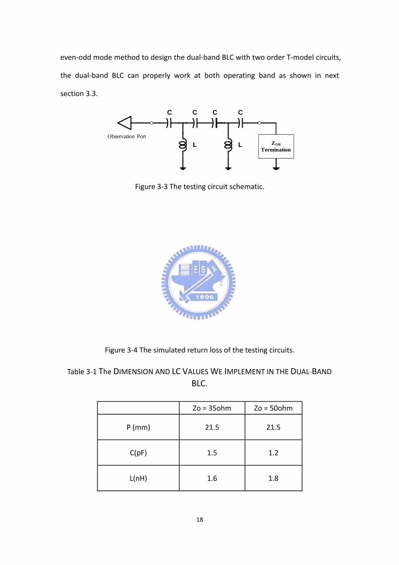

22
results are slightly different from the simulation results Fortunately the measured
bandwidth in each operating band is about 200MHz so it is still feasible for covering
each of the required bandwidth From Fig 3‐8 to Fig 13 the two output power in
WiMAX operation are lower than the two output power in WiFi operation Itrsquos caused
by the wavelength in WiMAX operation is shorter than the wavelength in WiFi
operation so the discontinuity area is increased and may affect the performance in
WiMAX operation
Figure 3‐7 Combination of the dual‐band BLC and two wideband switching circuits
Table 3‐2 THE OPERATING SENSE OF FOUR STATES OF COMBINATION OF THE
DUAL‐BAND BLC AND TWO WIDEBAND SWITHCING CIRCUITS
Intput Switching circuit (1) Switching circuit (2) Output
Case 1 Port 1 Through Termination Port2
Case 2 Port 1 Through Through Port2 and Port3
Case 3 Port 4 Termination Through Port3
Case 4 Port 4 Through Through Port2 and Port3
Figure 3‐8 The sim
(a)
(b) W
mulated resu
23
WiFi opera
WiMAX oper
ults of the d
ation
ration
dual‐band BBLC in Case
2 state
Figurre 3‐9 The s
(a)
(b) W
simulated re
24
WiFi opera
WiMAX oper
esults of du
ation
ration
al band BLCC in Case 4 s
state
Figure 3‐10 The
(a)
(b) W
e simulated
25
WiFi opera
WiMAX oper
angle differ
ation
ration
rence of thee dual‐band
d BLC
Figure 3‐11 MMeasured sc
with two
(a)
(b) W
cattering pa
wideband s
26
WiFi opera
WiMAX ope
arameters o
switching ci
ation
ration
of combinat
rcuits in Ca
ion of the d
se 2 state
dual‐band BBLC
Figgure 3‐12 Measured s
with two
(a)
(b) W
scattering p
wideband s27
WiFi opera
WiMAX ope
parameters
switching ci
ation
ration
of combina
rcuits in Ca
tion of the
se 4 state
dual‐band BLC
28
(a) WiFi operation
(b) WiMAX operation
Figure 3‐13 The measured angle difference of the dual‐band BLC
29
Chapter 4 Dual‐band Patch Antenna
In this chapter we will propose a square patch antenna fed by two L‐shaped
probe with four slots The two L‐shaped probes can effectively reduce the coupling
effect between two ports Moreover the square patch with four slots can make the
structure of the antenna symmetric and provide dual‐band operation
41 Antenna Design
The structure of slot is often adopted in the antenna design for either dual‐band
excitation or bandwidth enhancement As shown in Fig 4‐1 [18] they propose a
structure which consists of a rectangular patch loaded by two slots which are etched
close to the radiating edges where the bandwidth is about 2 in two operating
bands In this structure the slots are used to change the current of the TM30 mode
on the rectangular patch and make the current distribution become more similar
with the current distribution of TM10 and the current distribution in both operating
band are shown in Fig 4‐2 However because the patch is of the rectangular shape
it is hard to integrate two orthogonal linear polarization modes in a single patch
Moreover two directly‐fed coaxial probes in a single patch may cause serious
coupling as well
We therefore propose a square patch antenna fed by the L‐shaped probe with
four slots as shown in Fig 4‐3 The two slots along the X‐direction are parallel to the
X‐direction current distribution on the square patch so they will only disturb the
X‐direction current distribution slightly Because it is a symmetric structure we can
therefore utilize two L‐shaped probes feeding in orthogonal directions This
technique allows one square patch to set up two L‐shaped probes along X and Y
direction for producing two linear polarizations in a single patch and will not cause
30
serious coupling effect as well The geometric size of AH AG Lp Pw SL SG Sw we
implemented is 3mm 05mm 125mm 47mm 325mm 2mm and 06mm
respectively
Figure 4‐1 The probe‐fed patch antenna with a pair of slots
(a) (b) Figure 4‐2 The current distribution of the probe‐fed patch antenna with a pair of slots
(a) Lower band (b) Higher band
31
Figure 4‐3 Patch antenna fed by L‐shaped probe with four slots
42 Simulation and Measurement Results
The simulation and measurement results are shown in Fig 4‐4 The performance
of low S21 means coupling effect between two ports can be observed in both of the
desired frequency bands The simulated E‐plane radiation pattern at 245GHz and
35GHz are shown in Fig 4‐5 Because the magnitude of cross‐polarization pattern is
lower ‐10 dB it can be a good antenna candidate of linear polarization
Fig 4‐6 shows the measured radiation patterns The low cross polarization
represents that the additional two X‐direction slots only affect the X‐direction
current slightly The measured bandwidth and maximum gain are 244 and 923 dBi
at 245GHz respectively On the other hand the measured bandwidth and maximum
FR4 Substrate FR4 Substrate
Air
Feeding Line
Ground
Rectangular Patch
Ground
Feeding LineRectangular Patch
L-shaped probe
FR4 Substrate
FR4 Substrate
(a) Side view of L-shaped probe fed patch antenna
(b) Top view of L-shaped probe fed patch antenna with four slots
Slot
Slot
Slot
Slot
X
Y
Pw
SL
Lp
AH
AG
SwSG
gain
diffe
size
reas
n are 257
erent from
of the L‐s
sons make t
(a) T
(b) T
and 87 d
the simulat
haped prob
the patch m
The simulat
The measur
Bi at 35GH
ted results
bes and the
may not be f
ion result o
red result o32
z respectiv
It may be m
e gap betw
fabricated in
of the dual‐b
f the dual‐b
vely The me
mainly beca
ween the L‐
n the symm
band anten
band antenn
easured res
use of the d
‐shaped pro
metric mann
na in WiFi b
na in WiFi b
sults are slig
deviation of
obe The ab
er
band
band
ghtly
f the
bove
(c) Th
(d) Th
Figure 4‐4
he simulatio
he measure
The scatter
on result of
ed result of t
ring parame
two ortho
33
the dual‐ba
the dual‐ba
eters of the
ogonal L‐sh
and antenna
and antenna
patch ante
haped probe
a in WiMAX
a in WiMAX
enna with fo
es
X band
X band
our slots fedd by
34
-20 -15 -10 -5 0 5 10
45
-135
90
-90
135
-45
180 0
-20 -15 -10 -5 0 5 10
45
-135
90
-90
135
-45
180 0
(a) The simulated E‐plane radiation pattern at 245GHz
(b) The simulated E‐plane radiation pattern at 35GHz
Figure 4‐5 The simulated patterns of the patch antenna with four slots fed by two
orthogonal L‐shaped probes
Linear Polarization E‐plane-Co‐ -Cross
Linear Polarization E‐plane-Co‐ -Cross
35
-20 -15 -10 -5 0 5 10
45
-135
90
-90
135
-45
180 0
-20 -15 -10 -5 0 5 10
45
-135
90
-90
135
-45
180 0
(a) The measured E‐plane radiation pattern at 245GHz
(b) The measured E‐plane radiation pattern at 35GHz
Figure 4‐6 The measured patterns of the patch antenna with four slots fed by two
orthogonal L‐shaped probes
Linear Polarization E‐plane-Co‐ -Cross
Linear Polarization E‐plane-Co‐ -Cross
36
Chapter 5 The Dual‐band Reconfigurable
Quadri‐Polarization Diversity Antenna
We further combine the three parts (dual‐band BLC wideband switching circuit
and dual‐band patch antenna) which we have designed in the previous chapters and
present its performances The system block is shown in Fig 5‐1 As the wideband
switching circuit 1 and switching circuit 2 operate at ldquoThroughrdquo and ldquoTerminationrdquo
state respectively and the power is incident from port 1 the antenna can generate an
X‐directional linear polarization sense As the wideband switching circuit 1 and
switching circuit 2 both operate at ldquoThroughrdquo state and the power is incident from
port 1 the antenna can generate a left‐hand circular polarization sense in WiFi
operation In the same manner where the power is incidence from port4 the
antenna can generate a right‐hand circular polarization sense in WiFi operation The
operating modes of the proposed antenna are shown in Table 5‐1 From Table 5‐1
we find as the wideband switching circuits change their states the antenna structure
can provide quadri‐polarization in both operating bands
51 Simulation and Measurement Results
The top view of the whole simulated antenna structure in HFSS is shown in Fig
5‐2 The simulated scattering parameters in Case 1 (port 1 excitation) and Case 3
(port 2 excitation) state are shown in Fig 5‐3 and simulated scattering parameters of
Case 2 (port 1 excitation) and Case 4 (port 4 excitation) state are shown in Fig 5‐4
From the simulated scattering parameters we know the whole antenna structure is
feasible for covering each of the required bandwidth The simulated radiation
patterns of Case 1 are shown in Fig 5‐5 The simulated maximum gain in case 1 state
37
is 27dBi in WiFi and 22dBi in WiMAX operation respectively From the simulation
results since the cross‐polarization pattern is very small compared to the
co‐polarization pattern the antenna is convinced to have good operation in either
linear polarization or circular polarization
Figure 5‐1 The system block of the dual‐band antenna structure
38
Table 5‐1 STATUTES OF THE DUAL‐BAND ANTENNA STRUCTURE
Input Switching circuit (1) Switching circuit (2) Polarization sense
Case 1 Port 1 Through Termination X-direction
Linear Polarization
Case 2 Port 1 Through Through LHCP (WiFi operation)
RHCP (WiAX operation)
Case 3 Port 4 Termination Through Y-direction
Linear Polarization
Case 4 Port 4 Through Through RHCP (WiFi operation)
LHCP (WiAX operation)
The photograph of the antenna structure is shown in Fig 5‐6 The measured
performances of scattering parameters are shown in Fig 5‐7 and Fig 5‐8 and the
bandwidth is 57 and 6 in WiFi and WiMAX operation respectively The measured
radiation patterns are shown in Fig 5‐9 to Fig 5‐13 In Fig 5‐9 and Fig 5‐10 since
the cross‐polarization pattern is very small compared to the co‐polarization pattern
the dual‐band antenna is good for operating in linear polarization In Fig 5‐11a the
maximum gain is 25dBi and the 2‐dB axial‐ratio beamwidth is 86deg at 245GHz in Case
2 In Fig 5‐11b we can observe the maximum gain is about 19dBi and the 2‐dB
axial‐ratio beamwidth is 78deg at 35GHz in Case 2 The measured performances of the
dual‐band structure are listed in Table 5‐2 In Table5‐2 the quadri‐polarization
beamwidth means the axial‐ratio of LHCP and RHCP are lower than 2dB and the
magnitude of cross polarization of LP in Case 1 and Case 3 are lower than ‐10dB in
this beamwidth in each operating band
The measured maximum gain of Case 2 is little larger than the measured
maximum gain of Case 4 by 03dBi in 245GHz and 024dBi in 35GHz as shown in
Table 5‐2 To explain this phenomenon we must survey the power actually radiated
39
by the dual‐band patch antenna Therefore we have to get the scattering parameters
of the dual‐band patch antenna and dual‐band BLC individually In Section 3‐3 we
have got the simulated and measured scattering parameters of S21 and S31 which
can be considered A1 and A2 respectively the power incident to two L‐shaped probes
of the dual‐band patch antenna In Section 4‐2 we had simulated and measured
scattering parameters of the dual‐band patch antenna which can be considered a set
of SANT And the reflected power at Px and Py in Fig 5‐1 can be obtained by the
following equation
[ ] ⎥⎦
⎤⎢⎣
⎡sdot⎥
⎦
⎤⎢⎣
⎡=⎥
⎦
⎤⎢⎣
⎡sdot=⎥
⎦
⎤⎢⎣
⎡
2
1
2212
2111
2
1
2
1
AA
SSSS
AA
Sbb
ANT (5‐1)
where b1 and b2 is the quantity of reflected power at Px and Py respectively
Therefore the normalized power actually radiated by the dual‐band patch antenna is
2
22
12
22
1 bbAAP
PPi
ANTiANTi minusminus+== (5‐2)
where the Pi is the input power at port 1 or port 4 and the ANTiP is the power
actually radiated by the dual‐band patch antenna We first discuss the simulated
results of ANTiP In simulated results we get the parameters of A1 A2 and SANT and
substitute them into Equation (5‐2) We can therefore obtain b1 and b2 and the
normalized power ( ANTiP ) actually radiated by the dual‐band patch antenna is 0686
and 0685 in Case 2 and Case 4 state respectively in 245GHz In the same manner
we can get the normalized power ( ANTiP ) actually radiated by the dual‐band patch
antenna is 0554 and 0548 in Case 2 and Case 4 state respectively in 35GHz From
the computation results in both frequency bands because 1) the antenna structure is
symmetric 2) the lumped elements in HFSS are lossless and 3) the values of lumped
element donrsquot vary with frequency the power radiated by the dual‐band patch
antenna is almost equal in both of the two circular polarization states
40
Different from the simulated ones the measured A1 A2 and SANT can be gotten
from the previous chapter 3 and chapter 4 and we can use the same analysis
sequence to find the solutions of ANTiP The normalized power ( ANTiP ) actually
radiated by the dual‐band patch antenna is 0508 and 0403 in Case 2 and Case 4
state respectively in 245GHz and the normalized power ( ANTiP ) actually radiated by
the dual‐band patch antenna is 0462 and 0448 in Case 2 and Case 4 state
respectively in 35GHz Obviously the measured result ANTiP is lower than the
simulated result of ANTiP and itrsquos caused by the practical lumped elements provide
extra power loss Moreover the measured result of ANTiP in Case 4 is lower than the
measured result of ANTiP in Case 2 The calculated difference between Case 2 and
Case 4 is 006 in 245GHz and 008 in 35GHz so the measured maximum gain in Fig
5‐11 is slightly larger than the measured maximum gain in Fig 5‐12 by 022dBi in
245GHz and 024dBi in 35GHz The main reason of the imbalance may be that A1
and A2 of Case 2 is a little different from those of Case 4 at both frequency bands so
the actual radiated power of Case 2 and Case 4 will not be the same and result in the
asymmetric pattern gain at both frequency bands
Figure 5‐2 The top view of simulated antenna structure in HFSS
Figure 5‐33 The simul
(a)
(b) W
lated scatte
41
WiFi opera
WiMAX ope
ering param
ation
ration
eters in Casse 1 and Cas
se 3 state
Figure 5‐44 The simul
(a)
(b) W
lated scatte
42
WiFi opera
WiMAX ope
ering param
ation
ration
eters in Casse 2 and Cas
se 4 state
43
-20 -15 -10 -5 0 5
45
-135
90
-90
135
-45
180 0
-20 -15 -10 -5 0 5
45
-135
90
-90
135
-45
180 0
(a) 245GHz
(b) 35GHz
Figure 5‐5 The simulated radiation patterns in Case 1
Linear Polarization E‐plane-Co‐ -Cross
Linear Polarization E‐plane-Co‐ -Cross
44
(a) (b)
Figure 5‐6 The photographs of the dual‐band quadri‐polarization diversity patch
antenna (a) Front side of the structure (b) Back side of the structure
Figgure 5‐7 Thee measured
(a)
(b) W
d scattering
45
WiFi opera
WiMAX ope
parameters
and Case 3
ation
ration
s of the ant
enna struct
ture for Case 1
Figgure 5‐8 Thee measured
(a)
(b) W
d scattering
46
WiFi opera
WiMAX ope
parameters
and Case 4
ation
ration
s of the ant
enna struct
ture for Case 2
47
-20 -15 -10 -5 0 5
45
-135
90
-90
135
-45
180 0
-20 -15 -10 -5 0 5
45
-135
90
-90
135
-45
180 0
(a) The measured E‐plane radiation pattern at 245GHz
(b) The measured E‐plane radiation pattern at 35GHz
Figure 5‐9 The measured E‐plane radiation patterns in Case 1 state
Linear Polarization E‐plane-Co‐ -Cross
Linear Polarization E‐plane-Co‐ -Cross
48
-20 -15 -10 -5 0 5
45
-135
90
-90
135
-45
180 0
-20 -15 -10 -5 0 5
45
-135
90
-90
135
-45
180 0
(a) The measured E‐plane radiation pattern at 245GHz
(b) The measured E‐plane radiation pattern at 35GHz
Figure 5‐10 The measured E‐plane radiation patterns in Case 3 state
Linear Polarization E‐plane-Co‐ -Cross
Linear Polarization E‐plane-Co‐ -Cross
49
-20 -15 -10 -5 0 5
45
-135
90
-90
135
-45
180 0
-20 -15 -10 -5 0 5
45
-135
90
-90
135
-45
180 0
(a) Measured circular polarization radiation pattern at 245GHz
(b) Measured circular polarization radiation pattern at 35GHz
Figure 5‐11 The measured radiation patterns in Case 2 state
Circular Polarization- Gain
Circular Polarization- Gain
50
-20 -15 -10 -5 0 5
45
-135
90
-90
135
-45
180 0
-20 -15 -10 -5 0 5
45
-135
90
-90
135
-45
180 0
(a) Measured circular polarization radiation pattern at 245GHz
(b) Measured circular polarization radiation pattern at 35GHz
Figure 5‐12 The measured radiation patterns in Case 4 state
Circular Polarization- Gain
Circular Polarization- Gain
51
(a) 245GHz
(b) 35GHz
Figure 5‐13 The measured axial‐ratio of the proposed antenna
52
Table 5‐2 THE MEASURED PERFORMANCES OF THE DUAL‐BAND ANTENNA
STRUCTURE
Frequency Polarization
Sense
Axial Ratio lt 2
Beamwidth (Deg)
Quadri‐Polarization
Beamwidth (Deg)
Maxinum Gain
(dBi)
245GHz
RHCP (Case 4) 65
65
218 LHCP (Case 2) 90 24 LP (Case 1) XXX 23 LP (Case 3) XXX 2
35GHz
RHCP (Case 2) 95
70
18 LHCP (Case 4) 80 156 LP (Case 1) XXX 176 LP (Case 3) XXX 163
53
Chapter 6 Conclusion
We have provided another even‐odd mode method to design the dual‐band BLC
and combined it with the wideband switching circuits successfully in Chapter 3 With
the wideband switching circuit we can easily control the power to either go through
the circuit or be absorbed by 50‐Ohm termination from 2 GHz to 6 GHz The
dual‐band BLC provides two equal power signals with 90deg phase difference in two
operating bands In Chapter 4 a dual‐band patch antenna with low cross polarization
and coupling has been completely fabricated Because of the symmetry of the
antenna structure we proposed two L‐shaped probes can be easily integrated in a
single patch and the four additional slots are etched close to each radiation side to
produce another radiation frequency Finally we combine the above three parts to
fabricate a single patch antenna structure with dual‐band reconfigurable
quadri‐polarization diversity The measured results in Chapter 5 have shown our
proposed dual‐band quadric‐polarization diversity antenna meets our expectation
WiFi and WiMAX systems are becoming more popular in wireless communication
applications And one antenna structure operating in these two bands is becoming
more important Our antenna design can be one of the best solutions for enhancing
the communication quality The idea we present in this thesis is good but there is still
room for improvement to reach better performance First we may design a better
switching circuit to increase the antenna gain and reduce the lump elements
Moreover the design of the dual‐band quadri‐polarization diversity antenna is
convinced a rising topic and we provide one as a milestone for this demand We
believe the design of dual‐band quadri‐polarization diversity antenna will greatly
bring contribution to the communication technology
54
References
[1] 吳逸凡「新型可塑性四極化天線設計」國立交通大學碩士論文民國94
年
[2] 吳俊賢「可塑性四極化掃描天線之設計」國立交通大學碩士論文民國
95年
[3] W L Stutzman and G A Thiele Antenna Theory and Design 2nd ed New York
Wiley p 212‐215 1998
[4] C L Mak K M Luk K F Lee and Y L Chow ldquoExperimental Study of a Microstrip
Patch Antenna with an L‐shaped Proberdquo IEEE Trans Antenna amp Propagation vol
48 pp777‐783 May 2000
[5] I‐Hsiang Lin Marc DeVincentis Christophe Caloz and Tatsuo Itoh ldquoArbitrary
Dual‐Band Components Using Composite RightLeft ‐Handed Transmission Linesrdquo
IEEE Trans Microwave Theory and Techniques vol 52 pp 1142‐1149 Apr 2004
[6] K R Carver and J W Mink ldquoMicrostrip Antenna Technologyrdquo IEEE Trans
Antenna amp Propagation vol AP‐29 pp 2‐24 Jan 1981
[7] D H Schaubert ldquoMicrostrip Antennardquo Electromagnetics vol 12 pp 381‐401
July‐ December 1992
[8] R E Munson ldquoConformal Microstrip Antennas and Microstrip Phased Arraysrdquo
IEEE Trans Antennas amp Propagation vol AP‐22 pp74‐78 Jan 1974
[9] D R Jackson and N G Alexopoulos ldquoSimple Approximate Formulas for Input
Resistance Bandwidth and Efficiency of a Resonant Rectangular Patchrdquo IEEE
Trans Antennas amp Propagation vol 3 pp407‐410 Mar 1991
[10] R Q Lee K F Lee and J Bobinchak ldquoCharacteristics of a two‐layer
electromagnetically coupled rectangular patch antennardquo Electron Lett vol 23
pp 1070ndash1072 Sep 1987
55
[11] E Chang S A Long and W F Richards ldquoExperimental investigation of electrically
thick rectangular microstrip antennasrdquo IEEE Trans Antennas amp Propagation vol
AP‐43 pp 767ndash772 Jun 1986
[12] T M Au K F Tong and K M Luk ldquoCharacteristics of aperture‐coupled co‐planar
microstrip subarraysrdquo Inst Elect Eng Proc Microwave Antennas Propagat vol
144 pp 137ndash140 Apr 1997
[13] K M Luk C L Mak Y L Chow and K F Lee ldquoBroadband microstrip patch
antennardquo Electron Lett vol 34 pp 1442ndash1443 Jul 1998
[14] H Nakano M Yamazaki and J Yamauchi ldquoElectromagnetically coupled curl
antennardquo Electron Lett vol 33 pp 1003ndash1004 Jun 1997
[15] H Nakano M Yamazaki and J Yamauchi ldquoElectromagnetically coupled curl
antennardquo Electron Lett vol 33 pp 1003ndash1004 Jun 1997
[16] David M Pozar and Sean M Duffy ldquoA Dual‐Band Circular Polarized
Aperture‐Coupled Stacked Microstrip Antenna for Global Positioning Satelliterdquo
IEEE Trans Antennas amp Propagation vol 45 pp 1618‐1625 Nov 1997
[17] Stephen D Targonski and David M Pozar ldquoDesign of Wideband Circular
Polarized Aperture‐Coupled Microstrip Antennasrdquo IEEE Trans Antennas amp
Propagation vol 41 pp 214‐219 Feb 1993
[18] S Maci G B Gentili and G Avitabile ldquoSingle‐layer dual frequency patch
antennardquo Electron Lett vol 29 pp 1441‐1443 Aug 1993
- 封面pdf
- 羅馬pdf
- 內文_1-11_pdf
- 內文_12-28__paper版本_pdf
- 內文_29-35_pdf
- 內文_36-50_pdf
- 內文_51-52_pdf
- 內文_53-55_pdf
-
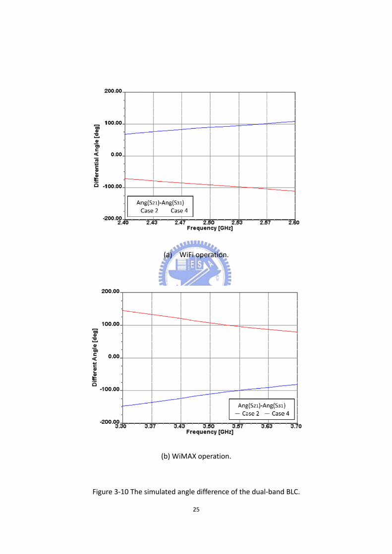
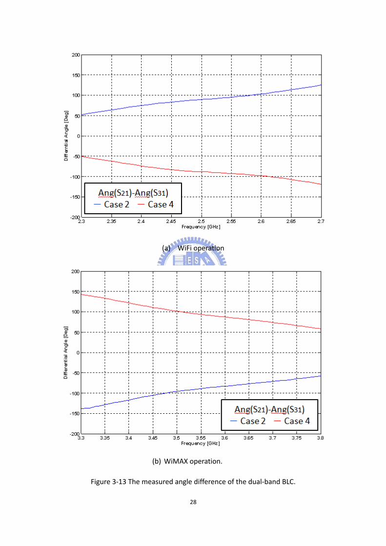
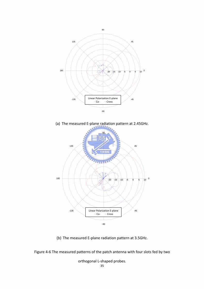
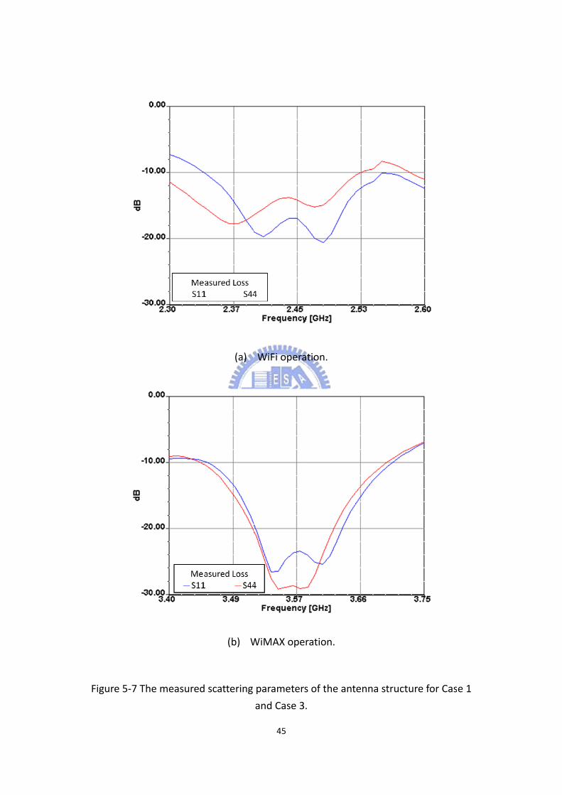
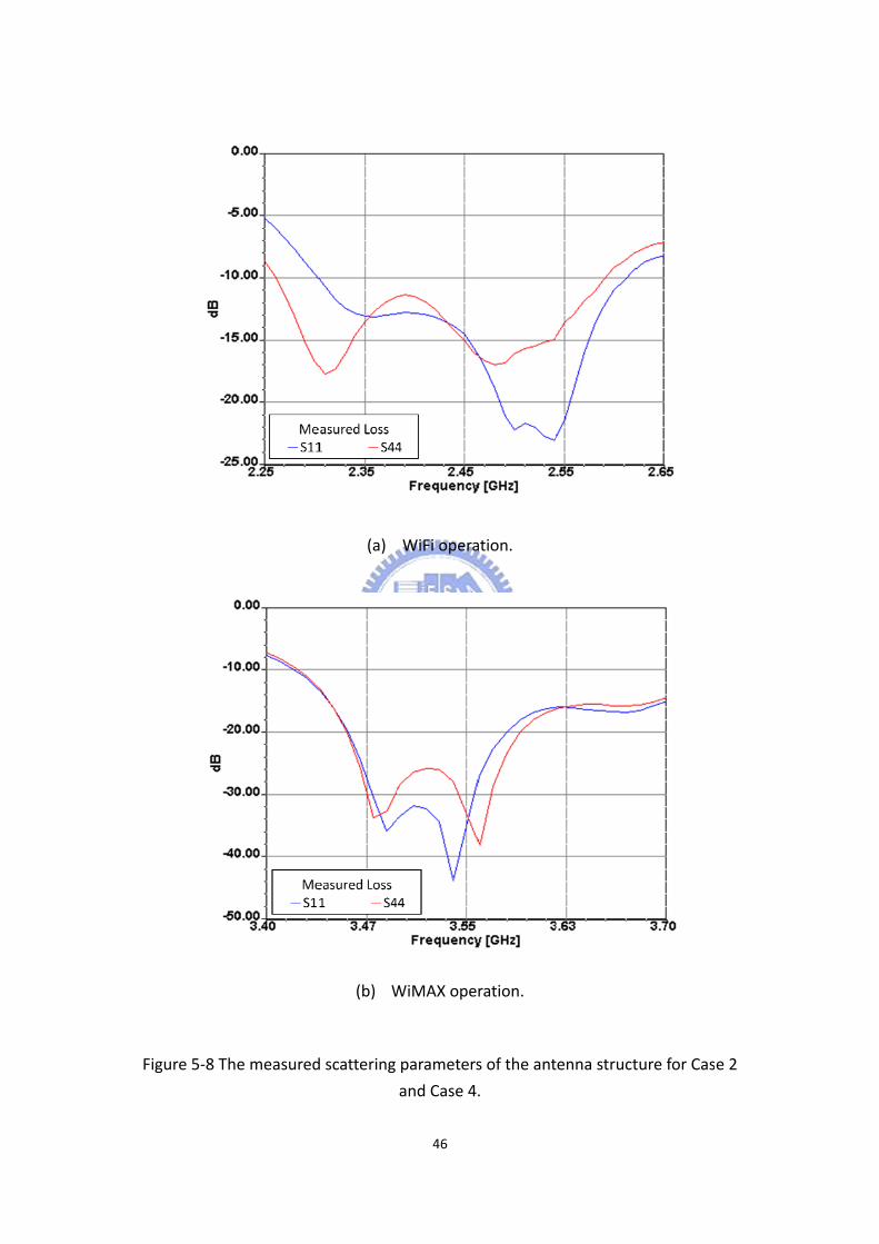
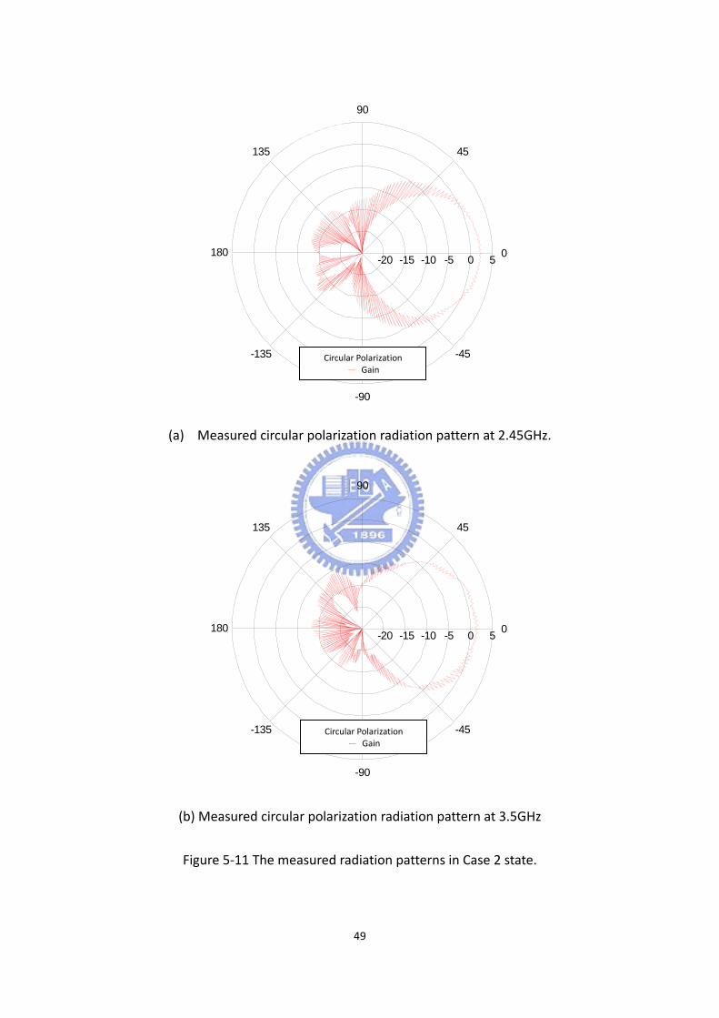