Obsolete Product(s) - Obsolete Product(s) - Home - … · Obsolete Product(s) - Obsolete Product(s)...
21
1/21 October 2004 ■ COMPLETE INTERFACE BETWEEN LNB AND I 2 C TM BUS ■ BUILT-IN DC/DC CONTROLLER FOR SINGLE 12V SUPPLY OPERATION ■ ACCURATE BUILT-IN 22KHz TONE OSCILLATOR ■ SUITS WIDELY ACCEPTED STANDARDS ■ FAST OSCILLATOR START-UP FACILITATES DiSEqC TM ENCODING ■ BUILT-IN 22KHz TONE DETECTOR SUPPORTS BI-DIRECTIONAL DiSEqC TM ■ LOOP-THROUGH FUNCTION FOR SLAVE OPERATION ■ LNB SHORT CIRCUIT PROTECTION AND DIAGNOSTIC ■ CABLE LENGTH DIGITAL COMPENSATION ■ INTERNAL OVER TEMPERATURE PROTECTION DESCRIPTION Intended for analog and digital satellite STB receivers/SatTV, sets/PC cards, the LNBS21 is a monolithic voltage regulator and interface IC, assembled in PowerSO-20, specifically designed to provide the power and the 13/18V, 22KHz tone signalling to the LNB downconverter in the antenna or to the multiswitch box. In this application field, it offers a complete solution with extremely low component count, low power dissipation together with simple design and I 2 C TM standard interfacing. This IC has a built in DC/DC step-up controller that, from a single supply source ranging from 8 to 15V, generates the voltages that let the linear LNBS21 LNB SUPPLY AND CONTROL IC WITH STEP-UP CONVERTER AND I 2 C INTERFACE Enable I Select Preregul.+ U.V.lockout +P.ON res. Feedback Step-up Controller V Select Linear Post-reg +Modulator +Protections 22KHz Oscill. Vup LT1 OUT SDA SCL DSQIN Vcc Diagnostics I²C interf. Tone Detector DSQOUT LT2 DETIN LNBS21 Byp Gate Sense EXTM ADDR Figure 1: Schematic Diagram PowerSO-20 Rev. 3 Obsolete Product(s) - Obsolete Product(s) Obsolete Product(s) - Obsolete Product(s)
Transcript of Obsolete Product(s) - Obsolete Product(s) - Home - … · Obsolete Product(s) - Obsolete Product(s)...

1/21October 2004
COMPLETE INTERFACE BETWEEN LNB AND I2CTM BUS
BUILT-IN DC/DC CONTROLLER FOR SINGLE 12V SUPPLY OPERATION
ACCURATE BUILT-IN 22KHz TONE OSCILLATOR
SUITS WIDELY ACCEPTED STANDARDS FAST OSCILLATOR START-UP FACILITATES
DiSEqCTM ENCODING BUILT-IN 22KHz TONE DETECTOR
SUPPORTS BI-DIRECTIONAL DiSEqCTM
LOOP-THROUGH FUNCTION FOR SLAVE OPERATION
LNB SHORT CIRCUIT PROTECTION AND DIAGNOSTIC
CABLE LENGTH DIGITAL COMPENSATION INTERNAL OVER TEMPERATURE
PROTECTION
DESCRIPTIONIntended for analog and digital satellite STBreceivers/SatTV, sets/PC cards, the LNBS21 is amonolithic voltage regulator and interface IC,
assembled in PowerSO-20, specifically designedto provide the power and the 13/18V, 22KHz tonesignalling to the LNB downconverter in theantenna or to the multiswitch box. In thisapplication field, it offers a complete solution withextremely low component count, low powerdissipation together with simple design and I2CTM
standard interfacing.This IC has a built in DC/DC step-up controllerthat, from a single supply source ranging from 8 to15V, generates the voltages that let the linear
LNBS21LNB SUPPLY AND CONTROL IC WITH
STEP-UP CONVERTER AND I2C INTERFACE
Enable
I Select
Preregul.+
U.V.lockout
+P.ON res.
FeedbackStep-upController
V Select
Linear Post-reg +Modulator +Protections
22KHz Oscill.
Vup
LT1
OUT
SDA
SCL
DSQIN
Vcc
Diagnostics
I²C interf.
Tone Detector
DSQOUT
LT2
DETIN
LNBS21
Byp
Gate
Sense
EXTM
ADDR
Figure 1: Schematic Diagram
PowerSO-20
Rev. 3
Obsolete Product(
s) - O
bsolete Product(
s)
O
bsolete Product(
s) - O
bsolete Product(
s)
Obsolete Product(
s) - O
bsolete Product(
s)
LNBS21
2/21
post-regulator to work at a minimum dissipatedpower. An UnderVoltage Lockout circuit willdisable the whole circuit when the supplied VCCdrops below a fixed threshold (6.7V typically). Theinternal 22KHz tone generator is factory trimmedin accordance to the standards, and can becontrolled either by the I2CTM interface or by adedicated pin (DSQIN) that allows immediateDiSEqCTM data encoding (*). All the functions ofthis IC are controlled via I2CTM bus by writing 6bits on the System Register (SR, 8 bits). Thesame register can be read back, and two bits willreport the diagnostic status. When the IC is put inStand-by (EN bit LOW), the power blocks aredisabled and the loop-through switch betweenLT1 and LT2 pins is closed, thus leaving all LNBpowering and control functions to the MasterReceiver (**). When the regulator blocks areactive (EN bit HIGH), the output can be logiccontrolled to be 13 or 18 V (typ.) by mean of theVSEL bit (Voltage SELect) for remote controllingof non-DiSEqC LNBs. Additionally, it is possible toincrement by 1V (typ.) the selected voltage valueto compensate for the excess voltage drop alongthe coaxial cable (LLC bit HIGH). In order tominimize the power dissipation, the output voltageof the internal step-up converter is adjusted toallow the linear regulator to work at minimumdropout. Another bit of the SR is addressed to theremote control of non-DiSEqC LNBs: the TEN(Tone ENable) bit. When it is set to HIGH, acontinuous 22KHz tone is generated regardless ofthe DSQIN pin logic status. The TEN bit must beset LOW when the DSQIN pin is used forDiSEqCTM encoding. The fully bi-directionalDiSEqCTM interfacing is completed by the built-in22KHz tone detector. Its input pin (DETIN) mustbe AC coupled to the DiSEqCTM bus, and theextracted PWK data are available on theDSQOUT pin (*).
In order to improve design flexibility and to allowimplementation of newcoming LNB remote controlstandards, an analogic modulation input pin isavailable (EXTM). An appropriate DC blockingcapacitor must be used to couple the modulatingsignal source to the EXTM pin. When externalmodulation is not used, the relevant pin can be leftopen.
The current limitation block has two thresholdsthat can be selected by the ISEL bit of the SR; thelower threshold is between 650 and 900mA(ISEL=HIGH), while the higher threshold isbetween 750 and 1000mA (ISEL=LOW).
The current protection block is SOA type. Thislimits the short circuit current (ISC) typically at300mA with ISEL=HIGH and at 400mA withISEL=LOW when the output port is connected toground.
It is possible to set the Short Circuit Currentprotection either statically (simple current clamp)or dynamically by the PCL bit of the SR; when thePCL (Pulsed Current Limiting) bit is set to LOW,the overcurrent protection circuit worksdynamically: as soon as an overload is detected,the output is shut-down for a time toff, typically900ms. Simultaneously the OLF bit of the SystemRegister is set to HIGH. After this time haselapsed, the output is resumed for a time ton=1/10toff (typ.). At the end of ton, if the overload is stilldetected, the protection circuit will cycle againthrough Toff and Ton. At the end of a full Ton inwhich no overload is detected, normal operation isresumed and the OLF bit is reset to LOW. TypicalTon+Toff time is 990ms and it is determined by aninternal timer. This dynamic operation can greatlyreduce the power dissipation in short circuitcondition, still ensuring excellent power-on startup in most conditions (**).
However, there could be some cases in which anhighly capacitive load on the output may cause adifficult start-up when the dynamic protection ischosen. This can be solved by initiating any powerstart-up in static mode (PCL=HIGH) and thenswitching to the dynamic mode (PCL=LOW) aftera chosen amount of time. When in static mode,the OLF bit goes HIGH when the current clamplimit is reached and returns LOW when theoverload condition is cleared.
This IC is also protected against overheating:when the junction temperature exceeds 150°C(typ.), the step-up converter and the linearregulator are shut off, the loop-trough switch isopened, and the OTF bit of the SR is set to HIGH.Normal operation is resumed and the OTF bit isreset to LOW when the junction is cooled down to140°C (typ.).
(*): External components are needed to comply to bi-directional DiSEqCTM bus hardware requirements. Full compliance of the whole appli-cation to DiSEqCTM specifications is not implied by the use of this IC.(**): The current limitation circuit has no effect on the loop-through switch. When EN bit is LOW, the current flowing from LT1 to LT2 must be externally limited.
O
bsolete Product(
s) - O
bsolete Product(
s)
Obsolete Product(
s) - O
bsolete Product(
s)
LNBS21
3/21
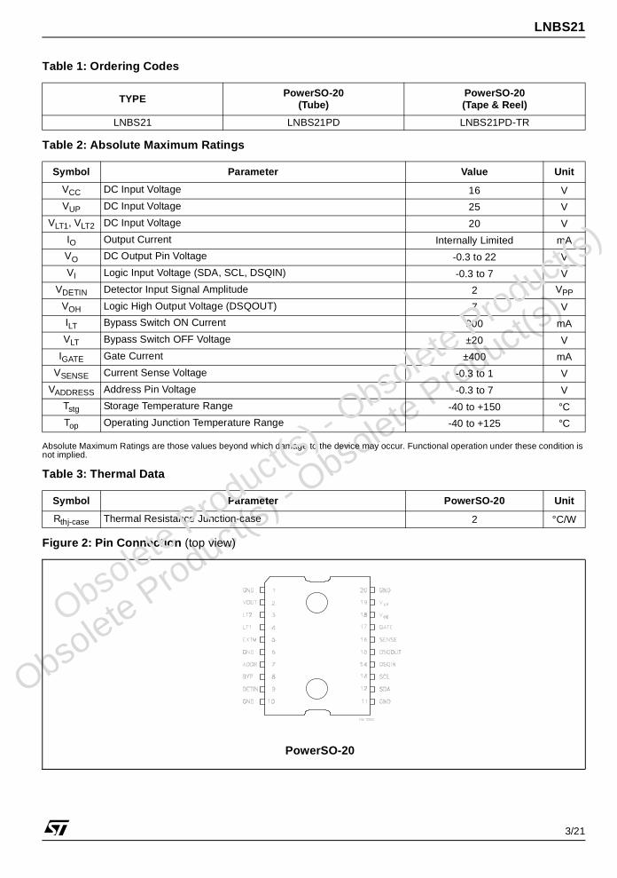
Table 1: Ordering Codes
Table 2: Absolute Maximum Ratings
Absolute Maximum Ratings are those values beyond which damage to the device may occur. Functional operation under these condition is not implied.
Table 3: Thermal Data
Figure 2: Pin Connection (top view)
TYPE PowerSO-20(Tube)
PowerSO-20(Tape & Reel)
LNBS21 LNBS21PD LNBS21PD-TR
Symbol Parameter Value Unit
VCC DC Input Voltage 16 V
VUP DC Input Voltage 25 V
VLT1, VLT2 DC Input Voltage 20 V
IO Output Current Internally Limited mA
VO DC Output Pin Voltage -0.3 to 22 V
VI Logic Input Voltage (SDA, SCL, DSQIN) -0.3 to 7 V
VDETIN Detector Input Signal Amplitude 2 VPP
VOH Logic High Output Voltage (DSQOUT) 7 V
ILT Bypass Switch ON Current 900 mA
VLT Bypass Switch OFF Voltage ±20 V
IGATE Gate Current ±400 mA
VSENSE Current Sense Voltage -0.3 to 1 V
VADDRESS Address Pin Voltage -0.3 to 7 V
Tstg Storage Temperature Range -40 to +150 °C
Top Operating Junction Temperature Range -40 to +125 °C
Symbol Parameter PowerSO-20 Unit
Rthj-case Thermal Resistance Junction-case 2 °C/W
PowerSO-20
O
bsolete Product(
s) - O
bsolete Product(
s)
Obsolete Product(
s) - O
bsolete Product(
s)
LNBS21
4/21
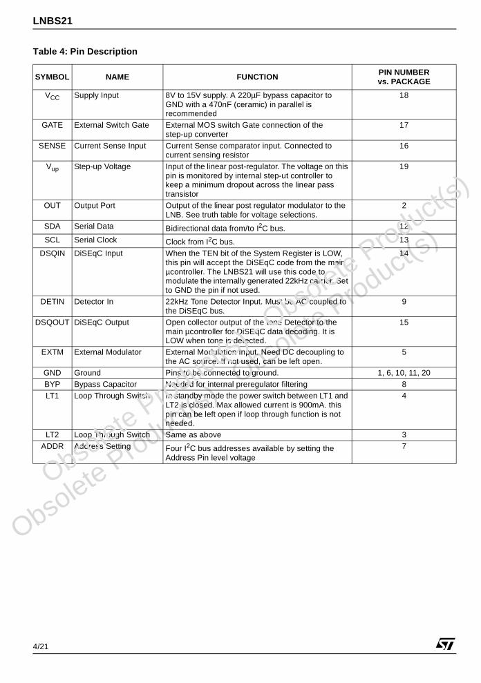
Table 4: Pin Description
SYMBOL NAME FUNCTION PIN NUMBER vs. PACKAGE
VCC Supply Input 8V to 15V supply. A 220µF bypass capacitor to GND with a 470nF (ceramic) in parallel is recommended
18
GATE External Switch Gate External MOS switch Gate connection of the step-up converter
17
SENSE Current Sense Input Current Sense comparator input. Connected to current sensing resistor
16
Vup Step-up Voltage Input of the linear post-regulator. The voltage on this pin is monitored by internal step-ut controller to keep a minimum dropout across the linear pass transistor
19
OUT Output Port Output of the linear post regulator modulator to the LNB. See truth table for voltage selections.
2
SDA Serial Data Bidirectional data from/to I2C bus. 12
SCL Serial Clock Clock from I2C bus. 13
DSQIN DiSEqC Input When the TEN bit of the System Register is LOW, this pin will accept the DiSEqC code from the main µcontroller. The LNBS21 will use this code to modulate the internally generated 22kHz carrier. Set to GND the pin if not used.
14
DETIN Detector In 22kHz Tone Detector Input. Must be AC coupled to the DiSEqC bus.
9
DSQOUT DiSEqC Output Open collector output of the tone Detector to the main µcontroller for DiSEqC data decoding. It is LOW when tone is detected.
15
EXTM External Modulator External Modulation Input. Need DC decoupling to the AC source. If not used, can be left open.
5
GND Ground Pins to be connected to ground. 1, 6, 10, 11, 20BYP Bypass Capacitor Needed for internal preregulator filtering 8LT1 Loop Through Switch In standby mode the power switch between LT1 and
LT2 is closed. Max allowed current is 900mA. this pin can be left open if loop through function is not needed.
4
LT2 Loop Through Switch Same as above 3ADDR Address Setting Four I2C bus addresses available by setting the
Address Pin level voltage7
O
bsolete Product(
s) - O
bsolete Product(
s)
Obsolete Product(
s) - O
bsolete Product(
s)
LNBS21
5/21
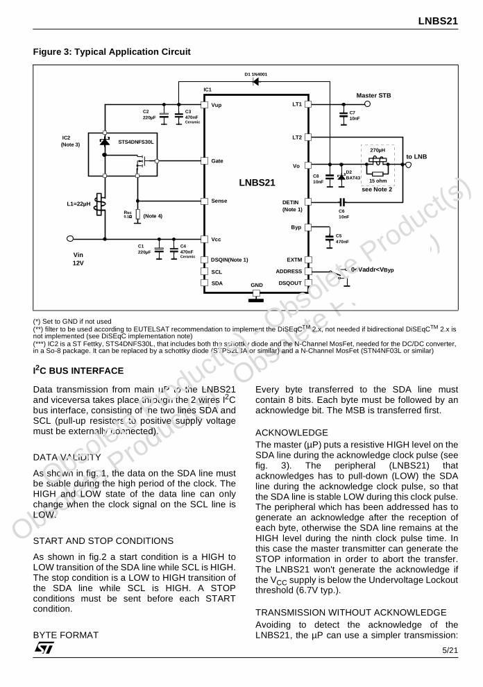
Figure 3: Typical Application Circuit
(*) Set to GND if not used(**) filter to be used according to EUTELSAT recommendation to implement the DiSEqCTM 2.x, not needed if bidirectional DiSEqCTM 2.x is not implemented (see DiSEqC implementation note)(***) IC2 is a ST Fettky, STS4DNFS30L, that includes both the schottky diode and the N-Channel MosFet, needed for the DC/DC converter, in a So-8 package. It can be replaced by a schottky diode (STPS2L3A or similar) and a N-Channel MosFet (STN4NF03L or similar)
I2C BUS INTERFACE
Data transmission from main µP to the LNBS21and viceversa takes place through the 2 wires I2Cbus interface, consisting of the two lines SDA andSCL (pull-up resistors to positive supply voltagemust be externally connected).
DATA VALIDITY
As shown in fig. 1, the data on the SDA line mustbe stable during the high period of the clock. TheHIGH and LOW state of the data line can onlychange when the clock signal on the SCL line isLOW.
START AND STOP CONDITIONS
As shown in fig.2 a start condition is a HIGH toLOW transition of the SDA line while SCL is HIGH.The stop condition is a LOW to HIGH transition ofthe SDA line while SCL is HIGH. A STOPconditions must be sent before each STARTcondition.
BYTE FORMAT
Every byte transferred to the SDA line mustcontain 8 bits. Each byte must be followed by anacknowledge bit. The MSB is transferred first.
ACKNOWLEDGEThe master (µP) puts a resistive HIGH level on theSDA line during the acknowledge clock pulse (seefig. 3). The peripheral (LNBS21) thatacknowledges has to pull-down (LOW) the SDAline during the acknowledge clock pulse, so thatthe SDA line is stable LOW during this clock pulse.The peripheral which has been addressed has togenerate an acknowledge after the reception ofeach byte, otherwise the SDA line remains at theHIGH level during the ninth clock pulse time. Inthis case the master transmitter can generate theSTOP information in order to abort the transfer.The LNBS21 won't generate the acknowledge ifthe VCC supply is below the Undervoltage Lockoutthreshold (6.7V typ.).
TRANSMISSION WITHOUT ACKNOWLEDGEAvoiding to detect the acknowledge of theLNBS21, the µP can use a simpler transmission:
270µH
15 ohm
see Note 2LNBS21
Vup
Gate
Vin12V
L1=22µH Sense
C2220µF
Vcc
LT1
Master STB
Vo
LT2
DETIN(Note 1)
C810nF
to LNB
SDA
SCL
DSQOUT
DSQIN(Note 1)
ADDRESS
Byp
C5470nF
GND
0<Vaddr<VByp
EXTM
C610nF
Rsc0.1ΩΩΩΩ
C3470nF Ceramic
D1 1N4001
C1220µF
C4470nF Ceramic
D2BAT43
C710nF
STS4DNFS30L IC2(Note 3)
IC1
(Note 4)
O
bsolete Product(
s) - O
bsolete Product(
s)

Obsolete Product(
s) - O
bsolete Product(
s)
LNBS21
6/21
simply it waits one clock without checking theslave acknowledging, and sends the new data.
This approach of course is less protected frommisworking and decreases the noise immunity.
Figure 4: Data Validity On The I2C Bus
Figure 5: Timing Diagram On I2C Bus
Figure 6: Acknowledge On I2C Bus
O
bsolete Product(
s) - O
bsolete Product(
s)

Obsolete Product(
s) - O
bsolete Product(
s)
LNBS21
7/21
LNBS1 SOFTWARE DESCRIPTION
INTERFACE PROTOCOL
The interface protocol comprises:
- A start condition (S)
- A chip address byte = hex 10 / 11 (the LSB bitdetermines read(=1)/write(=0) transmission)- A sequence of data (1 byte + acknowledge)- A stop condition (P)
ACK= AcknowledgeS= StartP= StopR/W= Read/Write
SYSTEM REGISTER (SR, 1 BYTE)
R,W= read and write bitR= Read-only bitAll bits reset to 0 at Power-On
TRANSMITTED DATA (I2C BUS WRITE MODE)When the R/W bit in the chip address is set to 0,the main µP can write on the System Register(SR) of the LNBS21 via I2C bus. Only 6 bits out of
the 8 available can be written by the µP, since theremaining 2 are left to the diagnostic flags, and areread-only.
X= don't care. Values are typical unless otherwise specified
RECEIVED DATA (I2C bus READ MODE)The LNBS21 can provide to the Master a copy ofthe SYSTEM REGISTER information via I2C busin read mode. The read mode is Master activatedby sending the chip address with R/W bit set to 1.At the following master generated clocks bits, theLNBS21 issues a byte on the SDA data bus line(MSB transmitted first).At the ninth clock bit the MCU master can:
- acknowledge the reception, starting in this waythe transmission of another byte from theLNBS21;
- no acknowledge, stopping the read modecommunication.
While the whole register is read back by the µP,only the two read-only bits OLF and OTF conveydiagnostic informations about the LNBS21.
CHIP ADDRESS DATA
MSB LSB MSB LSBS 0 0 0 1 0 0 0 R/W ACK ACK P
MSB LSBR, W R, W R, W R, W R, W R, W R RPCL ISEL TEN LLC VSEL EN OTF OLF
PCL ISEL TEN LLC VSEL EN OTF OLF Function
0 0 1 X X VOUT=13V, VUP=16V Loopthrough switch open
0 1 1 X X VOUT=18V, VUP=21V Loopthrough switch open
1 0 1 X X VOUT=14V, VUP=17V Loopthrough switch open
1 1 1 X X VOUT=19V, VUP=22V Loopthrough switch open
0 1 X X 22KHz tone is controlled by DSQIN pin1 1 X X 22KHz tone is ON, DSQIN pin disabled
0 1 X X IOUT(min)=500mA, IOUT(max)=650mA ISC=300mA
1 1 X X IOUT(min)=400mA, IOUT(max)=550mA ISC=300mA
0 1 X X Pulsed (dynamic) current limiting is selected1 1 X X Static current limiting is selectedX X X X X 0 X X Power blocks disabled, Loopthrough switch closed
O
bsolete Product(
s) - O
bsolete Product(
s)
Obsolete Product(
s) - O
bsolete Product(
s)
LNBS21
8/21
Values are typical unless otherwise specified
POWER-ON I2C INTERFACE RESETThe I2C interface built in the LNBS21 isautomatically reset at power-on. As long as theVCC stays be-low the UnderVoltage Lockoutthreshold (6.7V typ.), the interface will not respondto any I2C command and the System Register(SR) is initialized to all zeroes, thus keeping thepower blocks disabled. Once the VCC rises above7.3V, the I2C interface becomes operative and theSR can be configured by the main µP. This is dueto About 500mV of hysteresis provided in the UVLthreshold to avoid false retriggering of thePower-On reset circuit.
DiSEqCTM IMPLEMENTATIONThe LNBS21 helps the system designer toimplement the bi-directional (2.x) DiSEqC protocolby allowing an easy PWK modulation/demodulation of the 22KHz carrier. The PWK dataare exchanged between the LNBS21 and themain µP using logic levels that are compatible withboth 3.3 and 5V microcontrollers. This dataexchange is made through two dedicated pins,DSQIN and DSQOUT, in order to maintain thetiming relationships between the PWK data andthe PWK modulation as accurate as possible.These two pins should be directly connected totwo I/O pins of the µP, thus leaving to the residentfirmware the task of encoding and decoding the
PWK data in accordance to the DiSEqC protocol.Full compliance of the system to the specificationis thus not implied by the bare use of the LNBS21.
The system designer should also take inconsideration the bus hardware requirements,that include the source impedance of the MasterTransmitter measured at 22KHz. To limit theattenuation at carrier frequency, this impedancehas to be 15ohm at 22KHz, dropping to zero ohmat DC to allow the power flow towards theperipherals. This can be simply accomplished bythe LR termination put on the OUT pin of theLNBS, as shown in the Typical Application Circuiton page 5.
Unidirectional (1.x) DiSEqC and non-DiSEqCsystems normally don't need this termination, andthe OUT pin can be directly connected to the LNBsupply port of the Tuner. There is also no need ofTone Decoding, thus, it is recommended toconnect the DETIN and DSQOUT pins to groundto avoid EMI.
ADDRESS PIN
Connecting this pin to GND the Chip I2C interfaceaddress is 0001000, but, it is possible to choiceamong 4 different addresses simply setting thispin at 4 fixed voltage levels (see table on page10).
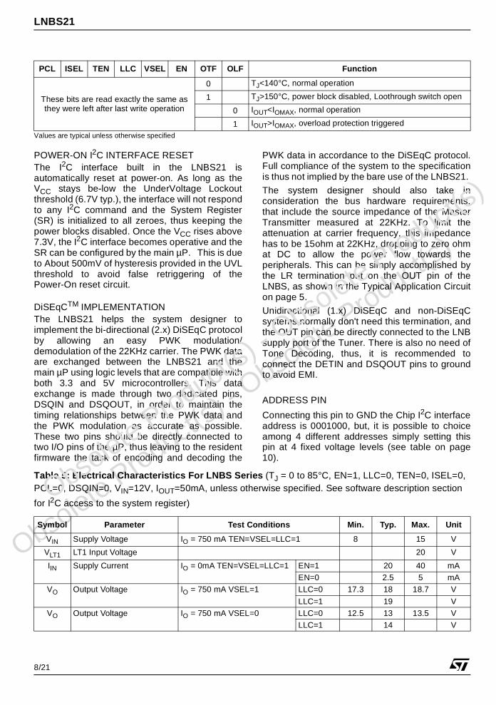
Table 5: Electrical Characteristics For LNBS Series (TJ = 0 to 85°C, EN=1, LLC=0, TEN=0, ISEL=0, PCL=0, DSQIN=0, VIN=12V, IOUT=50mA, unless otherwise specified. See software description section
for I2C access to the system register)
PCL ISEL TEN LLC VSEL EN OTF OLF Function
These bits are read exactly the same as they were left after last write operation
0 TJ<140°C, normal operation
1 TJ>150°C, power block disabled, Loothrough switch open
0 IOUT<IOMAX, normal operation
1 IOUT>IOMAX, overload protection triggered
Symbol Parameter Test Conditions Min. Typ. Max. Unit
VIN Supply Voltage IO = 750 mA TEN=VSEL=LLC=1 8 15 V
VLT1 LT1 Input Voltage 20 V
IIN Supply Current IO = 0mA TEN=VSEL=LLC=1 EN=1 20 40 mAEN=0 2.5 5 mA
VO Output Voltage IO = 750 mA VSEL=1 LLC=0 17.3 18 18.7 V
LLC=1 19 VVO Output Voltage IO = 750 mA VSEL=0 LLC=0 12.5 13 13.5 V
LLC=1 14 V
O
bsolete Product(
s) - O
bsolete Product(
s)

Obsolete Product(
s) - O
bsolete Product(
s)
LNBS21
9/21
∆VO Line Regulation VIN1=15 to 18V VSEL=0 5 40 mV
VSEL=1 5 60 mV∆VO Load Regulation VSEL=0 or 1 IOUT = 50 to 750mA 200 mV
IMAX Output Current Limiting ISEL=1 650 900 mAISEL=0 750 1000 mA
ISC Output Short Circuit Current ISEL=1 300 mAISEL=0 400 mA
tOFF Dynamic Overload protection OFF Time
PCL=0 Output Shorted 900 ms
tON Dynamic Overload protection ON Time
PCL=0 Output Shorted tOFF/10 ms
fTONE Tone Frequency TEN=1 20 22 24 KHz
ATONE Tone Amplitude TEN=1 0.55 0.72 0.9 Vpp
DTONE Tone Duty Cycle TEN=1 40 50 60 %
tr, tf Tone Rise and Fall Time TEN=1 5 10 15 µs
GEXTM External Modulation Gain ∆VOUT/∆VEXTM, f = 10Hz to 40KHz 6
VEXTM External Modulation Input Voltage
AC Coupling 400 mVpp
ZEXTM External Modulation Impedance
f = 10Hz to 50KHz 260 Ω
VLT Loopthrough Switch Voltage Drop (lt1 to LT2)
EN=0, ILT=300mA, VMI=12 or 19V
0.35 0.6 V
fSW DC/DC Converter Switch Frequency
220 kHz
fDETIN Tone Detector Frequency Capture Range
0.4Vpp sinewave 18 24 kHz
VDETIN Tone Detector Input Amplitude
fIN=22kHz sinewave 0.2 1.5 Vpp
ZDETIN Tone Detector Input Impedance
150 kΩ
VOL Overload Flag Pin Logic LOW
Tone present IOL=2mA 0.3 0.5 V
IOZ Overload Flag Pin OFF State Leakage Current
Tone absent VOH = 6V 10 µA
VIL DSQIN Input Pin Logic LOW
0.8 V
VIH DSQIN Input Pin Logic HIGH
2 V
IIH DSQIN Pins Input Current VIH = 5V 15 µA
IOBK Output Backward Current EN=0 VOBK = 18V -4 -10 mA
TSHDN Temperature Shutdown Threshold
150 °C
∆TSHDN Temperature Shutdown Hysteresis
15 °C
Symbol Parameter Test Conditions Min. Typ. Max. Unit
O
bsolete Product(
s) - O
bsolete Product(
s)
Obsolete Product(
s) - O
bsolete Product(
s)
LNBS21
10/21
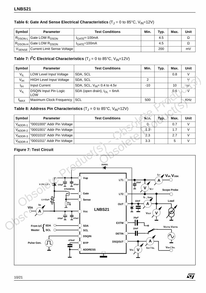
Table 6: Gate And Sense Electrical Characteristics (TJ = 0 to 85°C, VIN=12V)
Table 7: I2C Electrical Characteristics (TJ = 0 to 85°C, VIN=12V)
Table 8: Address Pin Characteristics (TJ = 0 to 85°C, VIN=12V)
Figure 7: Test Circuit
Symbol Parameter Test Conditions Min. Typ. Max. Unit
RDSON-L Gate LOW RDSON IGATE=-100mA 4.5 Ω
RDSON-H Gate LOW RDSON IGATE=100mA 4.5 Ω
VSENSE Current Limit Sense Voltage 200 mV
Symbol Parameter Test Conditions Min. Typ. Max. Unit
VIL LOW Level Input Voltage SDA, SCL 0.8 V
VIH HIGH Level Input Voltage SDA, SCL 2 V
IIH Input Current SDA, SCL, VIN= 0.4 to 4.5v -10 10 µA
VIL DSQIN Input Pin Logic LOW
SDA (open drain), IOL = 6mA 0.6 V
fMAX Maximum Clock Frequency SCL 500 KHz
Symbol Parameter Test Conditions Min. Typ. Max. Unit
VADDR-1 "0001000" Addr Pin Voltage 0 0.7 V
VADDR-2 "0001001" Addr Pin Voltage 1.3 1.7 V
VADDR-3 "0001010" Addr Pin Voltage 2.3 2.7 V
VADDR-4 "0001011" Addr Pin Voltage 3.3 5 V
Gate
VupLT1
OUT
Vcc
EXTM
DSQOUT
10nF
LT2
DETIN
10nF
Scope Probe
VMI, VOBK
LNBS21
470nFBYP
IO , IOBK
AVin
A
IIN
A
ILT
VVOUT
Load
20µF
V
A
IOZ / IOLOL
VOH / IOL
SDA
SCLSCL
SDAFrom I2C
Master
DSQIN
Pulse Gen.
VEXTM, VDETIN
Sense
STN4NF03L
Rsc0.1ΩΩΩΩ
220µF 470nF
STPS2L30A 220µF 470nF
L1=22µH
ADDRESS V
1N4001
V VLT
10nF
O
bsolete Product(
s) - O
bsolete Product(
s)

Obsolete Product(
s) - O
bsolete Product(
s)
LNBS21
11/21
TYPICAL CHARACTERISTICS (unless otherwise specified Tj = 25°C)
Figure 8: Output Voltage vs Temperature
Figure 9: Output Voltage vs Temperature
Figure 10: Line Regulation vs Temperature
Figure 11: Line Regulation vs Temperature
Figure 12: Load Regulation vs Temperature
Figure 13: Load Regulation vs Temperature
O
bsolete Product(
s) - O
bsolete Product(
s)
Obsolete Product(
s) - O
bsolete Product(
s)
LNBS21
12/21
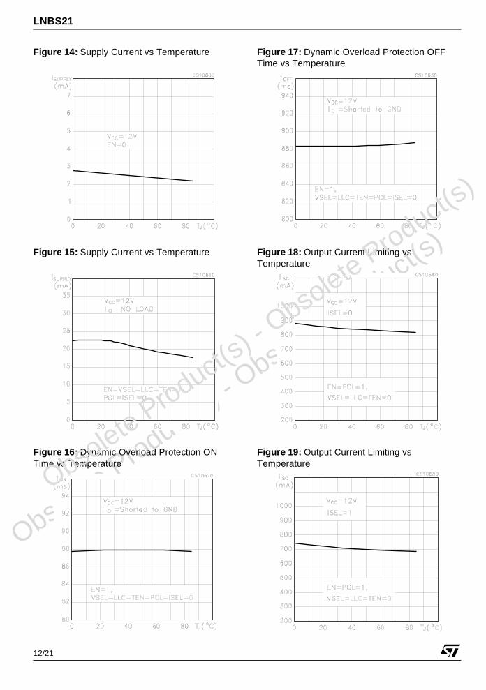
Figure 14: Supply Current vs Temperature
Figure 15: Supply Current vs Temperature
Figure 16: Dynamic Overload Protection ON Time vs Temperature
Figure 17: Dynamic Overload Protection OFF Time vs Temperature
Figure 18: Output Current Limiting vs Temperature
Figure 19: Output Current Limiting vs Temperature
O
bsolete Product(
s) - O
bsolete Product(
s)
Obsolete Product(
s) - O
bsolete Product(
s)
LNBS21
13/21
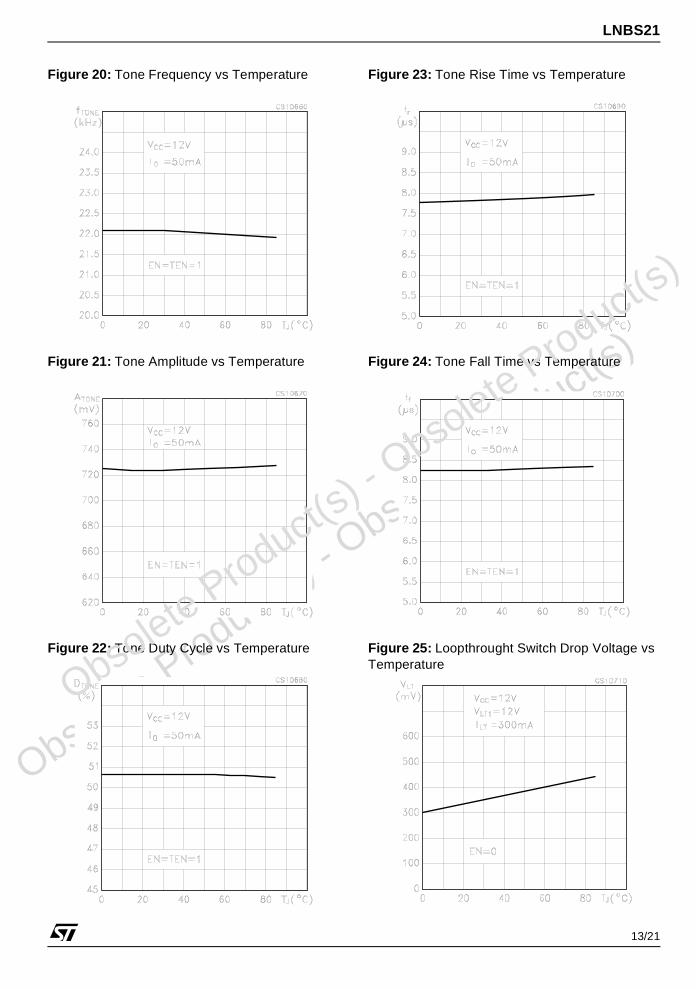
Figure 20: Tone Frequency vs Temperature
Figure 21: Tone Amplitude vs Temperature
Figure 22: Tone Duty Cycle vs Temperature
Figure 23: Tone Rise Time vs Temperature
Figure 24: Tone Fall Time vs Temperature
Figure 25: Loopthrought Switch Drop Voltage vs Temperature
O
bsolete Product(
s) - O
bsolete Product(
s)

Obsolete Product(
s) - O
bsolete Product(
s)
LNBS21
14/21
Figure 26: Loopthrought Switch Drop Voltage vs Temperature
Figure 27: Loopthrought Switch Drop Voltage vs Loopthrought Current
Figure 28: Loopthrought Switch Drop Voltage vs Loopthrought Current
Figure 29: DSQOUT Pin Logic Low vs Temperature
Figure 30: Undervoltage Lockout Threshold vs Temperature
Figure 31: Output Backward Current vs Temperature
O
bsolete Product(
s) - O
bsolete Product(
s)

Obsolete Product(
s) - O
bsolete Product(
s)
LNBS21
15/21
Figure 32: DC/DC Converter Efficiency vs Temperature
Figure 33: Current Limit Sense vs Temperature
Figure 34: 22kHz Tone
Figure 35: DSQIN Tone Enable Transient Response
Figure 36: DSQIN Tone Enable Transient Response
Figure 37: DSQIN Tone Disable Transient Response
VCC=12V, IO=50mA, EN=TEN=1
VCC=12V, IO=50mA, EN=1, TEN=0
VCC=12V, IO=50mA, EN=1, TEN=0
VCC=12V, IO=50mA, EN=1, TEN=0
O
bsolete Product(
s) - O
bsolete Product(
s)
Obsolete Product(
s) - O
bsolete Product(
s)
LNBS21
16/21
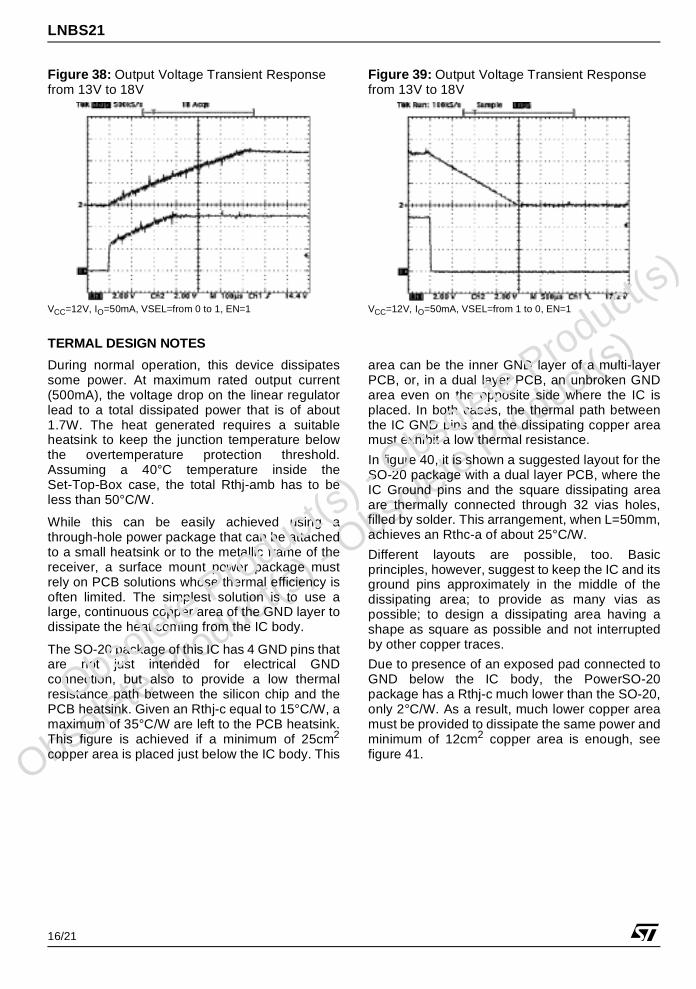
Figure 38: Output Voltage Transient Response from 13V to 18V
Figure 39: Output Voltage Transient Response from 13V to 18V
TERMAL DESIGN NOTES
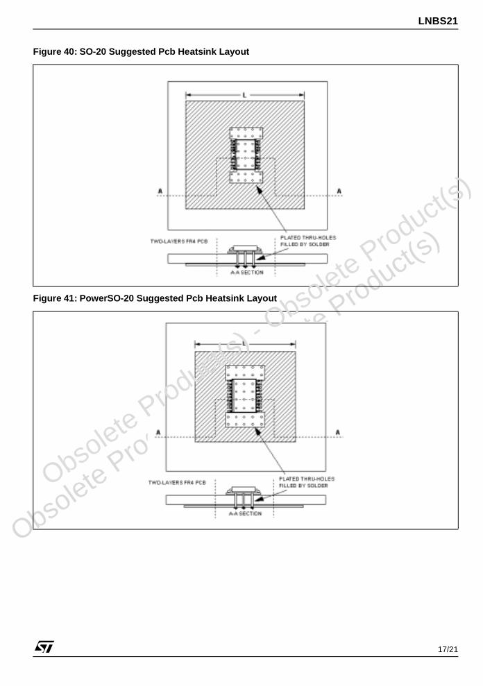
During normal operation, this device dissipatessome power. At maximum rated output current(500mA), the voltage drop on the linear regulatorlead to a total dissipated power that is of about1.7W. The heat generated requires a suitableheatsink to keep the junction temperature belowthe overtemperature protection threshold.Assuming a 40°C temperature inside theSet-Top-Box case, the total Rthj-amb has to beless than 50°C/W.
While this can be easily achieved using athrough-hole power package that can be attachedto a small heatsink or to the metallic frame of thereceiver, a surface mount power package mustrely on PCB solutions whose thermal efficiency isoften limited. The simplest solution is to use alarge, continuous copper area of the GND layer todissipate the heat coming from the IC body.
The SO-20 package of this IC has 4 GND pins thatare not just intended for electrical GNDconnection, but also to provide a low thermalresistance path between the silicon chip and thePCB heatsink. Given an Rthj-c equal to 15°C/W, amaximum of 35°C/W are left to the PCB heatsink.This figure is achieved if a minimum of 25cm2
copper area is placed just below the IC body. This
area can be the inner GND layer of a multi-layerPCB, or, in a dual layer PCB, an unbroken GNDarea even on the opposite side where the IC isplaced. In both cases, the thermal path betweenthe IC GND pins and the dissipating copper areamust exhibit a low thermal resistance.
In figure 40, it is shown a suggested layout for theSO-20 package with a dual layer PCB, where theIC Ground pins and the square dissipating areaare thermally connected through 32 vias holes,filled by solder. This arrangement, when L=50mm,achieves an Rthc-a of about 25°C/W.
Different layouts are possible, too. Basicprinciples, however, suggest to keep the IC and itsground pins approximately in the middle of thedissipating area; to provide as many vias aspossible; to design a dissipating area having ashape as square as possible and not interruptedby other copper traces.
Due to presence of an exposed pad connected toGND below the IC body, the PowerSO-20package has a Rthj-c much lower than the SO-20,only 2°C/W. As a result, much lower copper areamust be provided to dissipate the same power andminimum of 12cm2 copper area is enough, seefigure 41.
VCC=12V, IO=50mA, VSEL=from 0 to 1, EN=1 VCC=12V, IO=50mA, VSEL=from 1 to 0, EN=1
O
bsolete Product(
s) - O
bsolete Product(
s)
Obsolete Product(
s) - O
bsolete Product(
s)
LNBS21
17/21
Figure 40: SO-20 Suggested Pcb Heatsink Layout
Figure 41: PowerSO-20 Suggested Pcb Heatsink Layout
O
bsolete Product(
s) - O
bsolete Product(
s)

Obsolete Product(
s) - O
bsolete Product(
s)
LNBS21
18/21
DIM.mm. inch
MIN. TYP MAX. MIN. TYP. MAX.
A 3.60 0.1417
a1 0.10 0.30 0.0039 0.0118
a2 3.30 0.1299
a3 0 0.10 0 0.0039
b 0.40 0.53 0.0157 0.0209
c 0.23 0.32 0.0090 0.0013
D (1) 15.80 16.00 0.6220 0.630
E 13.90 14.50 0.5472 0.5710
e 1.27 0.0500
e3 11.43 0.4500
E1 (1) 10.90 11.10 0.4291 0.4370
E2 2.90 0.1141
G 0 0.10 0.0000 0.0039
h 1.10 0.0433
L 0.80 1.10 0.0314 0.0433
N 0˚ 10˚
S 0˚ 8˚ 0˚ 8˚
T 10.0 0.3937
PowerSO-20 MECHANICAL DATA
0056635
e
a2 A
E
a1
PSO20MEC
DETAIL A
T
D
1 1 0
1120
E1E2
h x 45
DETAIL Alead
sluga3
S
Gage Plane0.35
L
DETAIL B
R
DETAIL B
(COPLANARITY)
G C
- C-
SEATING PLANE
e3
b
c
NN
(1) “D and E1” do not include mold flash or protusions - Mold flash or protusions shall not exceed 0.15mm (0.006”)
1
O
bsolete Product(
s) - O
bsolete Product(
s)
Obsolete Product(
s) - O
bsolete Product(
s)
LNBS21
19/21
DIM.mm. inch
MIN. TYP MAX. MIN. TYP. MAX.
A 330 12.992
C 12.8 13.2 0.504 0.519
D 20.2 0.795
N 60 2.362
T 30.4 1.197
Ao 15.1 15.3 0.594 0.602
Bo 16.5 16.7 0.650 0.658
Ko 3.8 4.0 0.149 0.157
Po 3.9 4.1 0.153 0.161
P 23.9 24.1 0.941 0.949
W 23.7 24.3 0.933 0.957
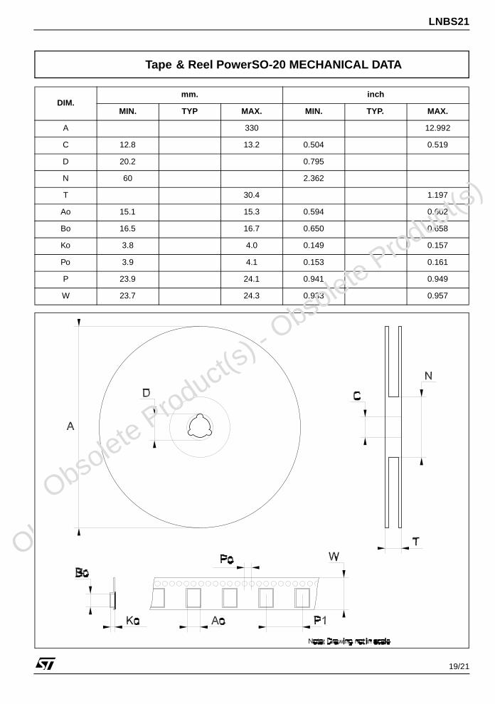
Tape & Reel PowerSO-20 MECHANICAL DATA
O
bsolete Product(
s) - O
bsolete Product(
s)
Obsolete Product(
s) - O
bsolete Product(
s)
LNBS21
20/21
Table 9: Revision History
Date Revision Description of Changes
05-Oct-2004 3 Mistake Pin 6 - Table 4.
O
bsolete Product(
s) - O
bsolete Product(
s)

Obsolete Product(
s) - O
bsolete Product(
s)
LNBS21
21/21
Information furnished is believed to be accurate and reliable. However, STMicroelectronics assumes no responsibility for the consequencesof use of such information nor for any infringement of patents or other rights of third parties which may result from its use. No license is grantedby implication or otherwise under any patent or patent rights of STMicroelectronics. Specifications mentioned in this publication are subjectto change without notice. This publication supersedes and replaces all information previously supplied. STMicroelectronics products are notauthorized for use as critical components in life support devices or systems without express written approval of STMicroelectronics.
The ST logo is a registered trademark of STMicroelectronics
All other names are the property of their respective owners
© 2004 STMicroelectronics - All Rights Reserved
STMicroelectronics group of companies
Australia - Belgium - Brazil - Canada - China - Czech Republic - Finland - France - Germany - Hong Kong - India - Israel - Italy - Japan - Malaysia - Malta - Morocco - Singapore - Spain - Sweden - Switzerland - United Kingdom - United States of America
www.st.com
O
bsolete Product(
s) - O
bsolete Product(
s)