Obsolete Product(s) - Obsolete Product(s) j-case Thermal Resistance Junction-case Max 2.5 C/W...
14
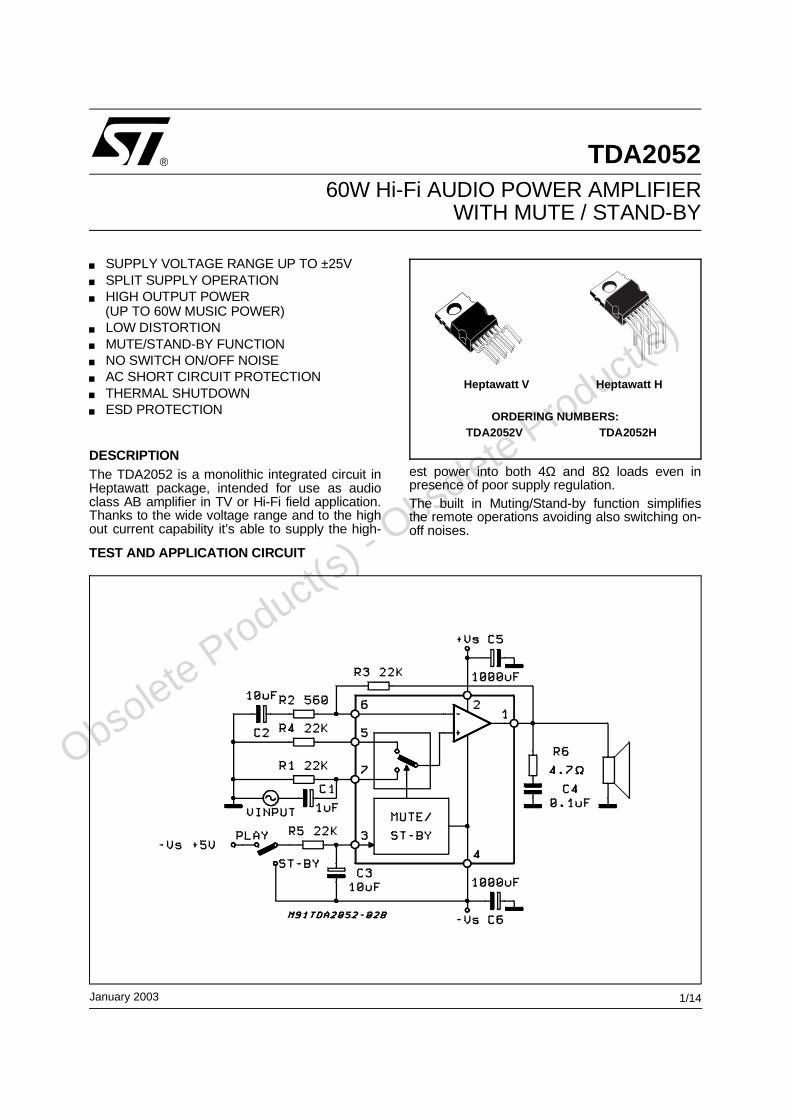
TDA2052 60W Hi-Fi AUDIO POWER AMPLIFIER WITH MUTE / STAND-BY SUPPLY VOLTAGE RANGE UP TO ±25V SPLIT SUPPLY OPERATION HIGH OUTPUT POWER (UP TO 60W MUSIC POWER) LOW DISTORTION MUTE/STAND-BY FUNCTION NO SWITCH ON/OFF NOISE AC SHORT CIRCUIT PROTECTION THERMAL SHUTDOWN ESD PROTECTION DESCRIPTION The TDA2052 is a monolithic integrated circuit in Heptawatt package, intended for use as audio class AB amplifier in TV or Hi-Fi field application. Thanks to the wide voltage range and to the high out current capability it’s able to supply the high- est power into both 4Ω and 8Ω loads even in presence of poor supply regulation. The built in Muting/Stand-by function simplifies the remote operations avoiding also switching on- off noises. This is advanced information on a new product now in development or undergoing evaluation. Details are subject to change without notice. January 2003 ® Heptawatt V Heptawatt H ORDERING NUMBERS: TDA2052V TDA2052H TEST AND APPLICATION CIRCUIT 1/14 Obsolete Product(s) - Obsolete Product(s)
Transcript of Obsolete Product(s) - Obsolete Product(s) j-case Thermal Resistance Junction-case Max 2.5 C/W...
TDA205260W Hi-Fi AUDIO POWER AMPLIFIER
WITH MUTE / STAND-BY
SUPPLY VOLTAGE RANGE UP TO ±25VSPLIT SUPPLY OPERATIONHIGH OUTPUT POWER(UP TO 60W MUSIC POWER)LOW DISTORTIONMUTE/STAND-BY FUNCTIONNO SWITCH ON/OFF NOISEAC SHORT CIRCUIT PROTECTIONTHERMAL SHUTDOWNESD PROTECTION
DESCRIPTIONThe TDA2052 is a monolithic integrated circuit inHeptawatt package, intended for use as audioclass AB amplifier in TV or Hi-Fi field application.Thanks to the wide voltage range and to the highout current capability it’s able to supply the high-
est power into both 4Ω and 8Ω loads even inpresence of poor supply regulation.The built in Muting/Stand-by function simplifiesthe remote operations avoiding also switching on-off noises.
This is advanced information on a new product now in development or undergoing evaluation. Details are subject to change without notice.
January 2003
®
Heptawatt V Heptawatt H
ORDERING NUMBERS: TDA2052V TDA2052H
TEST AND APPLICATION CIRCUIT
1/14
O
bsolete Product(
s) - O
bsolete Product(
s)
ABSOLUTE MAXIMUM RATINGS
Symbol Parameter Value Unit
VS DC Supply Voltage ±25 V
IO Output Peak Current (internally limited) 6 A
Ptot Power Dissipation Tcase = 70°C 30 W
Top Operating Temperature Range 0 to +70 °CTstg, Tj Storage and Junction Temperature -40 to +150 °C
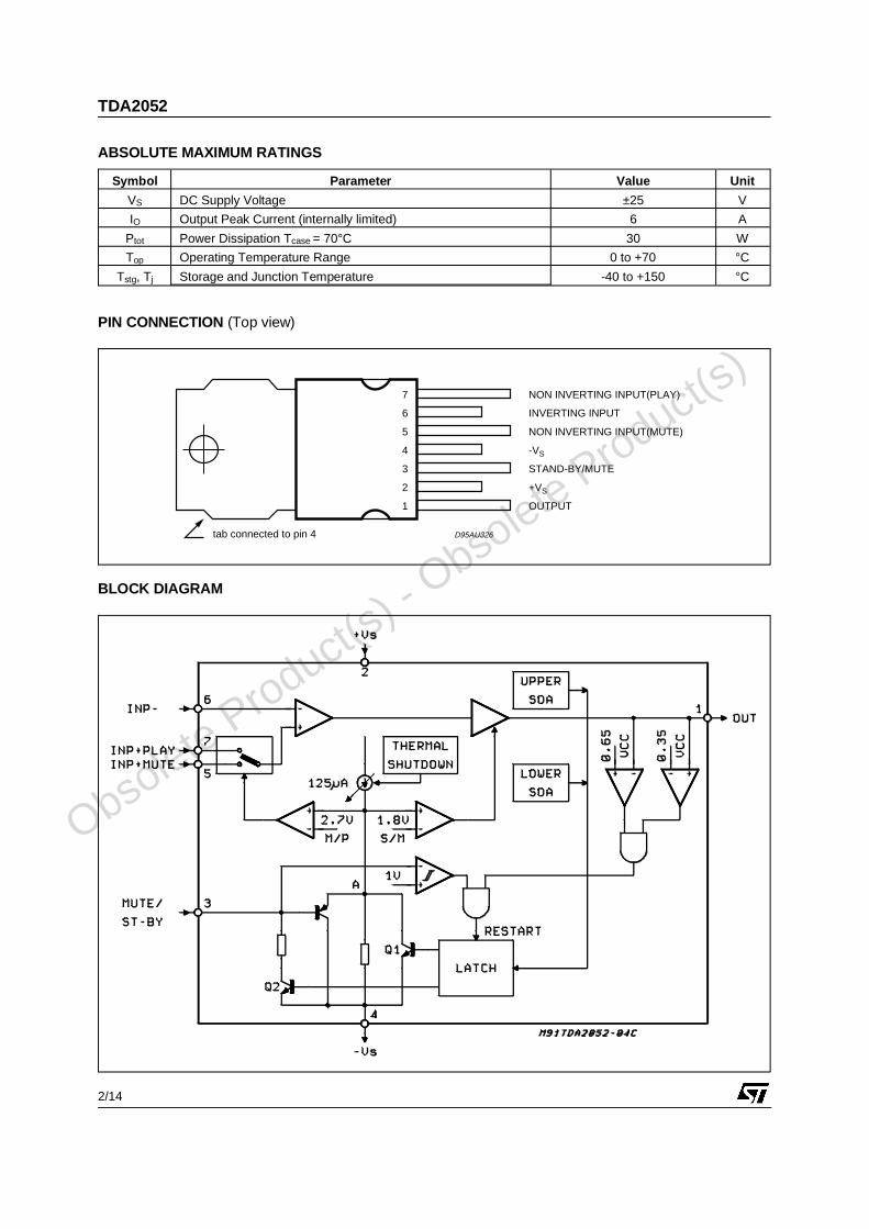
BLOCK DIAGRAM
1
2
3
4
5
6
7 NON INVERTING INPUT(PLAY)
INVERTING INPUT
-VS
STAND-BY/MUTE
+VS
OUTPUT
D95AU326tab connected to pin 4
NON INVERTING INPUT(MUTE)
PIN CONNECTION (Top view)
TDA2052
2/14
O
bsolete Product(
s) - O
bsolete Product(
s)
ELECTRICAL CHARACTERISTICS (Refer to the test circuit, GV = 32dB; VS + 18V; f = 1KHz; Tamb =25°C, unless otherwise specified.)
Symbol Parameter Test Condition Min. Typ. Max. Unit
VS Supply Range +6 +25 V
Iq Total Quiescent Current VS = +22V 20 40 70 mA
Ib Input Bias Current +0.5 µA
VOS Input Offset Voltage +15 mV
IOS Input Offset Current +200 nA
PO Music Output PowerIEC268-3 Rules (*)
VS = + 22.5, RL = 4Ω, d = 10%, t = 1s 50 60 W
PO Output Power (continuous RMS) d = 10%RL = 4ΩRL = 8ΩVS = +22V, RL = 8Ω
35
30
402233
WWW
d = 1%RL = 4ΩRL = 8ΩVS = +22V, RL = 8Ω
321728
WWW
d Total Harmonic Distortion RL = 4ΩPO = 0.1 to 20W; f = 100Hz to 15KHz
VS + 22V, RL = 8ΩPO = 0.1 to 20W; f = 100Hz to 15KHz
0.1
0.1
0.7
0.5
%
%
SR Slew Rate 3 5 V/µs
GV Open Loop Voltage Gain 80 dB
eN Total Input Noise A Curvef = 20Hz to 20KHz
23 10
µVµV
Ri Input Resistance 500 KΩSVR Supply Voltage Rejection f = 100Hz, Vripple = 1VRMS 40 50 dB
TS Thermal Shutdown 145 °C
MUTE/STAND-BY FUNCTION (Ref. –VS)
VTST-BY Stand-by - Threshold 1 1.8 V
VTPLAY Play Threshold 2.7 4 V
Iq ST-BY Quiescent Current @ Stand-by Vpin 3 = 0.5V 1 3 mA
ATTST-BY Stand-by Attenuation 70 90 dB
Ipin3 Pin 3 Current @ Stand-by –1 +10 µA
Note (*):MUSIC POWER CONCEPTMUSIC POWER is ( according to the IEC clauses n.268-3 of Jan 83) the maximal power which the amplifier is capable of producing across therated load resistance (regardless of non linearity) 1 sec after the application of a sinusoidal input signal of frequency 1KHz.
According to this definition our method of measurement comprises the following steps:1) Set the voltage supply at the maximum operating value -10%2) Apply a input signal in the form of a 1KHz tone burst of 1 sec duration; the repetition period of the signal pulses is > 60 sec3) The output voltage is measured 1 sec from the start of the pulse4) Increase the input voltage until the output signal show a THD = 10%5) The music power is then V2
out/R1, where Vout is the output voltage measured in the condition of point 4) and R1 is the rated load impedance
The target of this method is to avoid excessive dissipation in the amplifier.
THERMAL DATA
Symbol Description Value Unit
Rth j-case Thermal Resistance Junction-case Max 2.5 °C/W
TDA2052
3/14
O
bsolete Product(
s) - O
bsolete Product(
s)
APPLICATIONS SUGGESTIONS (See Test and Application Circuit)The recommended values of the external components are those shown on the application circuit. Differ-ent values can be used; the following table can help the designer.
Comp. Value Purpose Larger Than Smaller Than
R1 22KΩ (*) Input Impedance Increase of InputImpedance
Decrease of InputImpedance
R2 560Ω Closed Loop Gain set to32dB (**)
Decrease of Gain Increase of Gain
R3 22KΩ (*) Increase of Gain Decrease of Gain
R4 22KΩ (*) Input Impedance @ Mute
R5 22KΩ Stand-by Time Constant
R6 4.7Ω Frequency Stability Danger of oscillations Danger of oscillations
C1 1µF Input DC Decoupling Higher Low-frequencycut-off
C2 10µF Feedback DC Decoupling Higher Low-frequencycut-off
C3 10µF Stand-by Time Constant
C4 0.100µF Frequency Stability Danger of Oscillations
C5, C6 1000µF Supply Voltage Bypass
(*) R1 = R3 = R4 for POP optimization
(**) Closed Loop Gain has to be ≥ 30dB
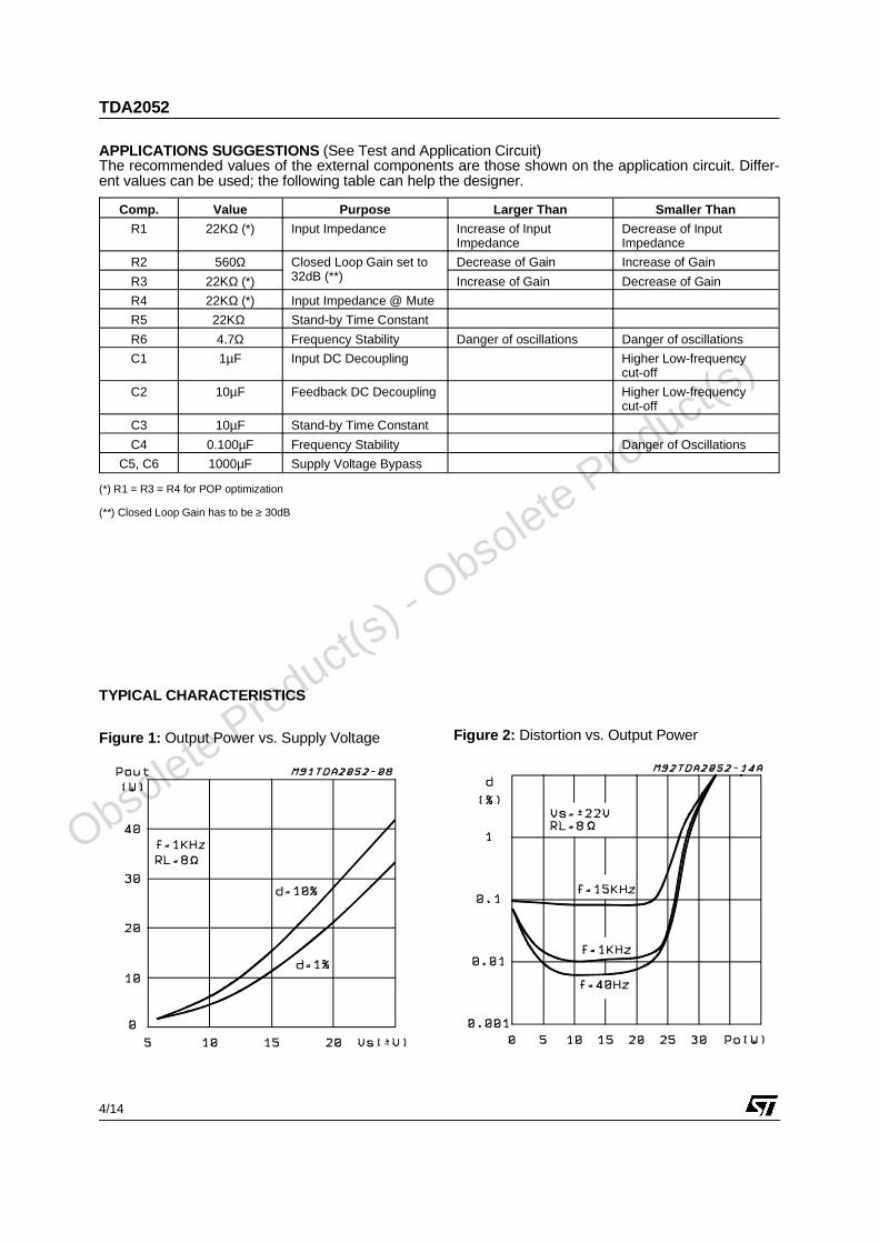
Figure 1: Output Power vs. Supply Voltage Figure 2: Distortion vs. Output Power
TYPICAL CHARACTERISTICS
TDA2052
4/14
O
bsolete Product(
s) - O
bsolete Product(
s)
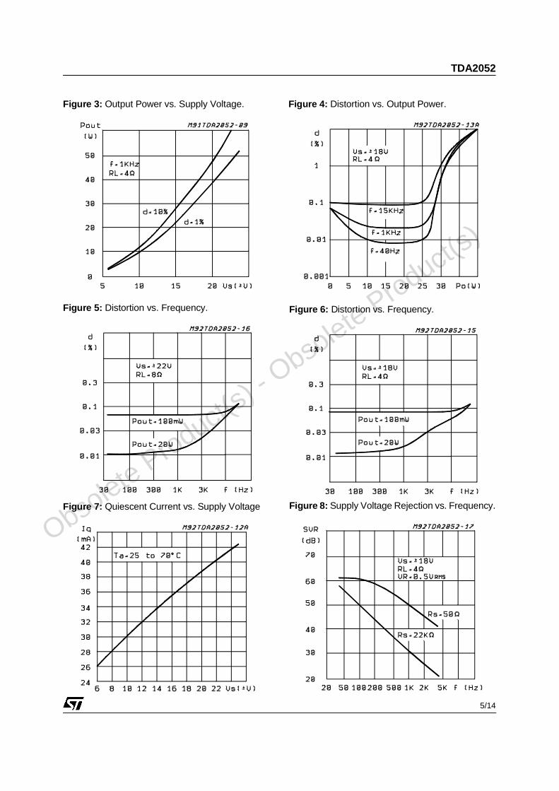
Figure 3: Output Power vs. Supply Voltage. Figure 4: Distortion vs. Output Power.
Figure 5: Distortion vs. Frequency. Figure 6: Distortion vs. Frequency.
Figure 7: Quiescent Current vs. Supply Voltage Figure 8: Supply Voltage Rejection vs. Frequency.
TDA2052
5/14
O
bsolete Product(
s) - O
bsolete Product(
s)
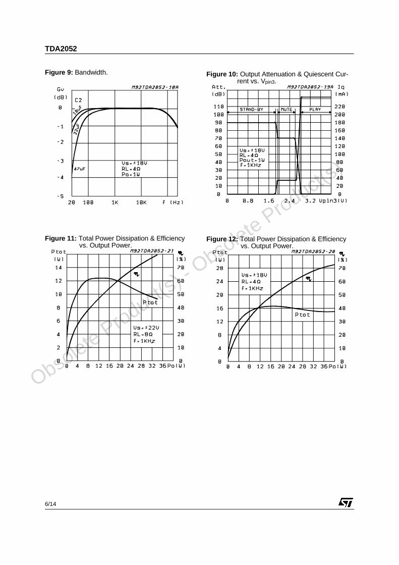
Figure 9: Bandwidth. Figure 10: Output Attenuation & Quiescent Cur-rent vs. Vpin3.
Figure 11: Total Power Dissipation & Efficiencyvs. Output Power.
Figure 12: Total Power Dissipation & Efficiencyvs. Output Power.
TDA2052
6/14
O
bsolete Product(
s) - O
bsolete Product(
s)
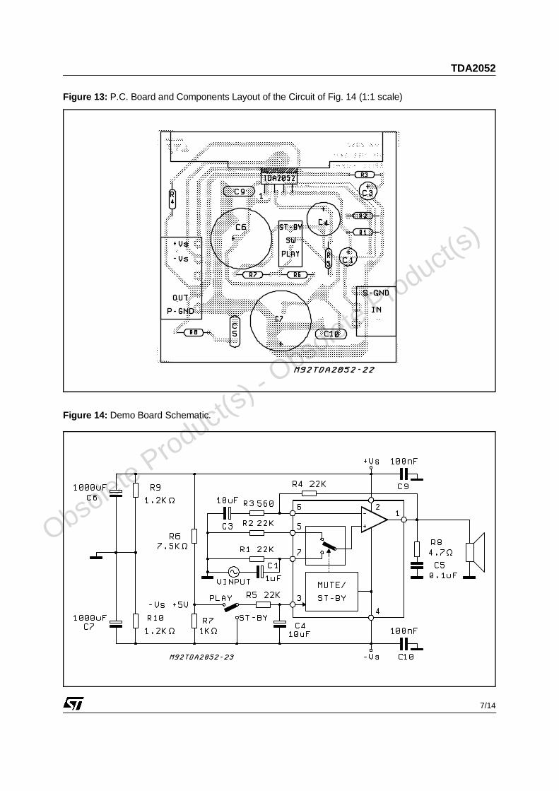
Figure 13: P.C. Board and Components Layout of the Circuit of Fig. 14 (1:1 scale)
Figure 14: Demo Board Schematic.
TDA2052
7/14
O
bsolete Product(
s) - O
bsolete Product(
s)
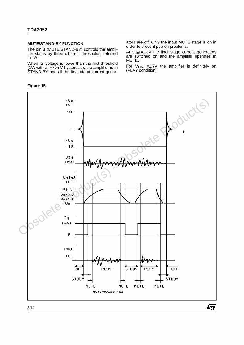
MUTE/STAND-BY FUNCTIONThe pin 3 (MUTE/STAND-BY) controls the ampli-fier status by three different thresholds, referredto -VS.When its voltage is lower than the first threshold(1V, with a +70mV hysteresis), the amplifier is inSTAND-BY and all the final stage current gener-
ators are off. Only the input MUTE stage is on inorder to prevent pop-on problems.At Vpin3=1.8V the final stage current generatorsare switched on and the amplifier operates inMUTE.For Vpin3 =2.7V the amplifier is definitely on(PLAY condition)
Figure 15.
TDA2052
8/14
O
bsolete Product(
s) - O
bsolete Product(
s)
SHORT-CIRCUIT PROTECTIONThe TDA 2052 has an original circuit which pro-tects the device during accidental short-circuit be-tween output and GND / -Vs / +Vs, taking it inSTAND-BY mode, so limiting also dangerous DCcurrent flowing throught the loudspeaker.If a short-circuit or an overload dangerous for thefinal transistors are detected, the concerned SOAcircuit sends out a signal to the latching circuit(with a 10µs delay time that prevents fast randomspikes from inadvertently shutting the amplifieroff) which makes Q1 and Q2 saturate (see BlockDiagram). Q1 immediately short-circuits to groundthe A point turning the final stage off while Q2short-circuits to ground the external capacitordriving the pin 3 (Mute/Stand-by) towards zeropotential. Only when the pin 3 voltage becomes lower than1V, the latching circuit is allowed to reset itselfand restart the amplifier, provided that the short-circuit condition has been removed. In fact, a win-dow comparator is present at the output and it isaimed at preventing the amplifier from restarting ifthe output voltage is lower than 0.35 Total SupplyVoltage or higher than 0.65 Total Supply Voltage.If the output voltage lies between these twothresholds, one may reasonably suppose theshort-circuit has been removed and the amplifiermay start operating again.The PLAY/MUTE/STAND-BY function pin (pin 3)is both ground- and positive supply-compatibleand can be interfaced by means of the R5, C3 neteither to a TTL or CMOS output (µ-Processor) orto a specific application circuit. The R5, C3 net is fundamental, because connect-ing this pin directly to a low output impedancedriver such as TTL gate would prevent the correctoperation during a short-circuit. Actually a finalstage overload turns on the protection latchingcircuit that makes Q2 try to drive the pin 3 voltageunder 0.8 V. Since the maximum current this pincan stand is 3 mA, one must make sure the fol-lowing condition is met:
R5 ≥ (VA − 0.7V)
3mA
that yields: R5, min = 1.5 KΩ with VA=5V.In order to prevent pop-on and -off transients, it isadvisable to calculate the C3, R5 net in such away that the STAND-BY/MUTE and MUTE/PLAYthreshold crossing slope (positive at the turn-onand vice-versa) is less than 100 V/sec.
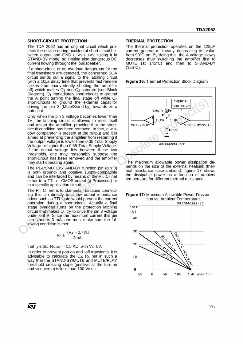
Figure 16: Thermal Protection Block Diagram
THERMAL PROTECTIONThe thermal protection operates on the 125µAcurrent generator, linearly decreasing its valuefrom 90°C on. By doing this, the A voltage slowlydecreases thus switching the amplifier first toMUTE (at 145°C) and then to STAND-BY(155°C).
Figure 17: Maximum Allowable Power Dissipa-tion vs. Ambient Temperature.
The maximum allowable power dissipation de-pends on the size of the external heatsink (ther-mal resistance case-ambient); figure 17 showsthe dissipable power as a function of ambienttemperature for different thermal resistance.
TDA2052
9/14
O
bsolete Product(
s) - O
bsolete Product(
s)
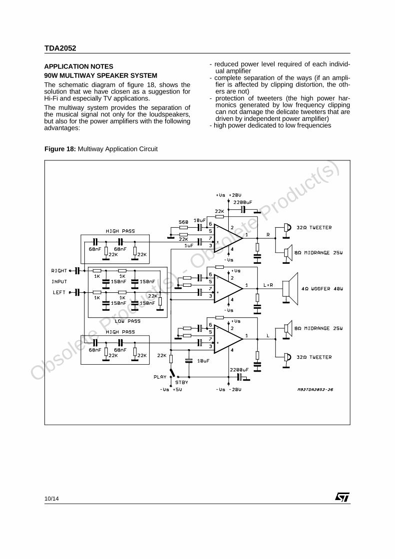
Figure 18: Multiway Application Circuit
APPLICATION NOTES 90W MULTIWAY SPEAKER SYSTEMThe schematic diagram of figure 18, shows thesolution that we have closen as a suggestion forHi-Fi and especially TV applications.The multiway system provides the separation ofthe musical signal not only for the loudspeakers,but also for the power amplifiers with the followingadvantages:
- reduced power level required of each individ-ual amplifier
- complete separation of the ways (if an ampli-fier is affected by clipping distortion, the oth-ers are not)
- protection of tweeters (the high power har-monics generated by low frequency clippingcan not damage the delicate tweeters that aredriven by independent power amplifier)
- high power dedicated to low frequencies
TDA2052
10/14
O
bsolete Product(
s) - O
bsolete Product(
s)
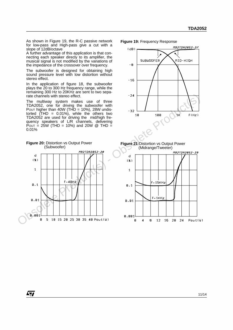
Figure 21: Distortion vs Output Power(Midrange/Tweeter)
Figure 20: Distortion vs Output Power(Subwoofer)
Figure 19: Frequency ResponseAs shown in Figure 19, the R-C passive networkfor low-pass and High-pass give a cut with aslope of 12dB/octaveA further advantage of this application is that con-necting each speaker direcly to its amplifier, themusical signal is not modified by the variations ofthe impedance of the crossover over frequency.The subwoofer is designed for obtaining highsound pressure level with low distortion withoutstereo effect.In the application of figure 18, the subwooferplays the 20 to 300 Hz frequency range, while theremaining 300 Hz to 20KHz are sent to two sepa-rate channels with stereo effect.The multiway system makes use of threeTDA2052, one for driving the subwoofer withPOUT higher than 40W (THD = 10%), 28W undis-torted (THD = 0.01%), while the others twoTDA2052 are used for driving the mid/high fre-quency speakers of L/R channels, deliveringPOUT = 25W (THD = 10%) and 20W @ THD =0.01%
TDA2052
11/14
O
bsolete Product(
s) - O
bsolete Product(
s)
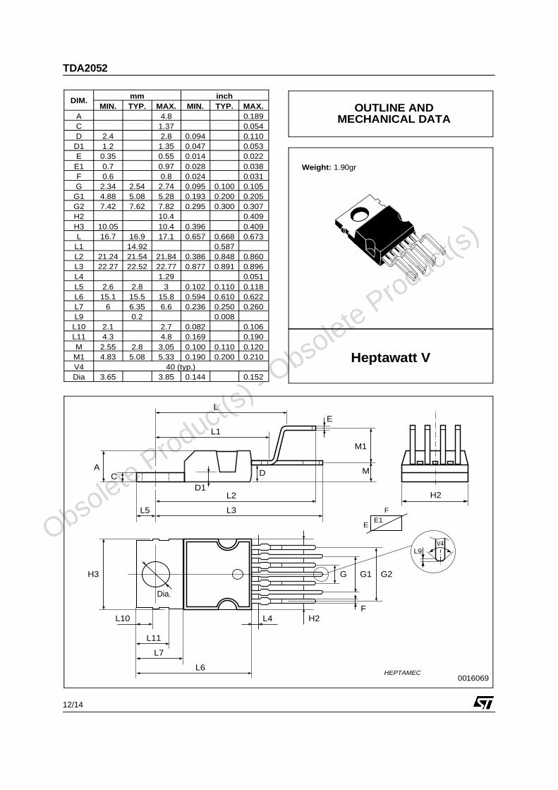
Weight: 1.90gr
Heptawatt V
DIM. mm inchMIN. TYP. MAX. MIN. TYP. MAX.
A 4.8 0.189C 1.37 0.054D 2.4 2.8 0.094 0.110
D1 1.2 1.35 0.047 0.053E 0.35 0.55 0.014 0.022
E1 0.7 0.97 0.028 0.038F 0.6 0.8 0.024 0.031G 2.34 2.54 2.74 0.095 0.100 0.105
G1 4.88 5.08 5.28 0.193 0.200 0.205G2 7.42 7.62 7.82 0.295 0.300 0.307H2 10.4 0.409H3 10.05 10.4 0.396 0.409L 16.7 16.9 17.1 0.657 0.668 0.673
L1 14.92 0.587L2 21.24 21.54 21.84 0.386 0.848 0.860L3 22.27 22.52 22.77 0.877 0.891 0.896L4 1.29 0.051L5 2.6 2.8 3 0.102 0.110 0.118L6 15.1 15.5 15.8 0.594 0.610 0.622L7 6 6.35 6.6 0.236 0.250 0.260L9 0.2 0.008
L10 2.1 2.7 0.082 0.106L11 4.3 4.8 0.169 0.190M 2.55 2.8 3.05 0.100 0.110 0.120
M1 4.83 5.08 5.33 0.190 0.200 0.210V4 40 (typ.)Dia 3.65 3.85 0.144 0.152
A
L
L1
CD1
L5
L2
L3
D
E
M1
M
H3
Dia.
L7
L11
L10
L6
H2F
G G1 G2
E1F
E
L9V4
L4
H2
HEPTAMEC 0016069
OUTLINE ANDMECHANICAL DATA
TDA2052
12/14
O
bsolete Product(
s) - O
bsolete Product(
s)

OUTLINE ANDMECHANICAL DATA
L2L3
E
DV5
C A
F
L7
L6
L4H2
F
L5
L10
L11
H3
HEPTHMEC.EPS
Dia.
L1 L9
G
G1
G2
H2
D1
E1F
E
Resin betweenleads
DIM.mm inch
MIN. TYP. MAX. MIN. TYP. MAX.
A 4.80 0.188
C 1.37 0.054
D 2.40 2.80 0.094 0.11
D1 1.20 1.35 0.047 0.053
E 0.35 0.55 0.014 0.022
E1 0.70 0.97 0.03 0.036
F 0.60 0.80 0.024 0.031
G 2.34 2.54 2.74 0.092 0.1 0.108
G1 4.88 5.08 5.28 0.192 0.2 0.208
G2 7.42 7.62 7.8 0.292 0.3 0.307
H2 10.40 0.41
H3 10.05 10.40 0.395 0.409
L1 3.90 4.20 4.50 0.153 0.165 0.177
L2 18.10 18.40 18.70 0.712 0.724 0.736
L3 4.88 5.08 5.28 0.192 0.2 0.208
L4 1.29 0.05
L5 2.60 3.00 0.102 0.118
L6 15.10 15.80 0.594 0.622
L7 6.00 6.60 0.236 0.260
L9 3.9 4.2 4.5 0.153 0.165 0.177
L10 2.10 2.70 0.083 0.106
L13 4.30 4.80 0.169 0.189
V5 89˚ (Min.), 90˚ (Typ.), 91˚ (Max.)
DIA 3.65 3.85 0.143 0.151
Heptawatt H
0080180
TDA2052
13/14
O
bsolete Product(
s) - O
bsolete Product(
s)
Information furnished is believed to be accurate and reliable. However, STMicroelectronics assumes no responsibility for the consequencesof use of such information nor for any infringement of patents or other rights of third parties which may result from its use. No license isgranted by implication or otherwise under any patent or patent rights of STMicroelectronics. Specification mentioned in this publication aresubject to change without notice. This publication supersedes and replaces all information previously supplied. STMicroelectronics productsare not authorized for use as critical components in life support devices or systems without express written approval of STMicroelectronics.
The ST logo is a registered trademark of STMicroelectronics© 2003 STMicroelectronics – Printed in Italy – All Rights Reserved
STMicroelectronics GROUP OF COMPANIESAustralia - Brazil - Canada - China - Finland - France - Germany - Hong Kong - India - Israel - Italy - Japan - Malaysia - Malta - Morocco -
Singapore - Spain - Sweden - Switzerland - United Kingdom - United States.http://www.st.com
TDA2052
14/14
O
bsolete Product(
s) - O
bsolete Product(
s)