Novel Packaging to Reduce Stray Inductance in Power Electronics - US Department of Energy ·...
15
Novel Packaging to Reduce Stray Inductance in Power Electronics PI: Leon Tolbert Presenter: Shengnan Li Oak Ridge National Laboratory June 10, 2010 Project ID: APE022 This presentation does not contain any proprietary, confidential, or otherwise restricted information
Transcript of Novel Packaging to Reduce Stray Inductance in Power Electronics - US Department of Energy ·...

Novel Packaging to Reduce Stray
Inductance in Power Electronics
PI: Leon TolbertPresenter: Shengnan Li
Oak Ridge National LaboratoryJune 10, 2010
Project ID: APE022
This presentation does not contain any proprietary, confidential, or otherwise restricted information

2 Managed by UT-Battellefor the U.S. Department of Energy
Overview
• Start Date: Oct. 2009• End Date: Sept. 2012• 20% Complete
• Barriers:– Accurately measuring:
• Module parasitics • Device stresses inside the module
– Reduce side effect caused by added inductance for dead time minimization
– Integration of the inductance into the trace.
• Target: Reduced voltage stress on IGBTs of the traction drive inverter. • DOE Share – 100%
• FY10 received: $348K
Timeline
Budget
Barriers
• The University of Tennessee• MaxQ Technology, LLC (module
fabrication)
Partners

3 Managed by UT-Battellefor the U.S. Department of Energy
Objective• Package devices in large power modules such
that stray inductance is reduced.– Increase inverter reliability– Increase device capability, reduce inverter cost
• FY10 – Extract parasitics in conventional and proposed power
module using electromagnetic-field simulation tool– Model and simulate IGBT switching behavior with
extracted parasitics– Build a prototype of a 10 kW IGBT single phase leg
module using the proposed packaging method

4 Managed by UT-Battellefor the U.S. Department of Energy
Milestone
• August 2010: Build phase leg module using proposed packaging method, measure and compare parasitics with conventional module.
• Go/No Go – If extracted parasitic inductance using Q3D extractor is smaller than conventional module, proceed.

5 Managed by UT-Battellefor the U.S. Department of Energy
Approach and Strategy• Series combination of switch and diode forms basic switching
cells, N-cell and P-cell, which can be used to construct all commonly used DC-DC and DC-AC converters. Use p-cell and n-cell concept to change packaging technique. IGBT and diode are packaged in a series arrangement instead of anti-parallel.
• By adding inductors between a P-cell and N-cell in a phase leg, dead time requirement can be reduced.
• For inverter application, vertical layout of N-cell and P-cell could be exploited for further integration.

6 Managed by UT-Battellefor the U.S. Department of Energy
• Ansoft Q3D extractor is used to perform electromagnetic-field simulation of package to extract parasitics.
• Saber is used for circuit simulation after getting the parasitic model.
• Prototype of proposed package will be built; impedance analyzer and V-I method will be used to measure the parasitics in P-cell and N-cell modules.
Approach and Strategy (cont’d)

7 Managed by UT-Battellefor the U.S. Department of Energy
FY10 Technical Accomplishments
• Package for phase leg modeled using Ansoft Q3D Extractor
Conventional phase leg package Proposed phase leg package

8 Managed by UT-Battellefor the U.S. Department of Energy
FY10 Technical Accomplishments (Cont’d)
• Extracted parasitic resistance and inductanceConventional phase leg package Proposed phase leg packageLoop 1: R = 8.36mΩ, L = 56.06nHLoop 2: R = 7.81mΩ, L = 52.67nHS1 emitter to D2 cathode:
R = 3.18mΩ, L = 22.19nHS2 collector to D1 anode:
R = 3.24mΩ, L = 23.36nH
Loop 1: R = 6.44mΩ, L = 39.91nHLoop 2: R = 5.62mΩ, L = 36.18nHS1 emitter to D2 cathode:
R = 1.26mΩ, L = 4.23nHS2 collector to D1 anode:
R = 0.04mΩ, L = 2.14nH

9 Managed by UT-Battellefor the U.S. Department of Energy
• Saber simulation is conducted usingthe parasitics extracted from Q3D
FY10 Technical Accomplishments (Cont’d)
Double pulse test circuit
Conventionalmodule
Proposed module
lp1 15.3 nH 17 nH
lp2 11.4 nH 1.07 nH
lp3 11.4 nH 1.07 nH
lp4 15.3 nH 17 nH
Parasitic Inductance Values

10 Managed by UT-Battellefor the U.S. Department of Energy
FY10 Technical Accomplishments (Cont’d)
Turn off overshoot voltage
Proposed module
Conventional module
• Simulation resultsfor turn off voltage ΔVconventional = 243 V ΔVproposed = 200 V
11 Managed by UT-Battellefor the U.S. Department of Energy
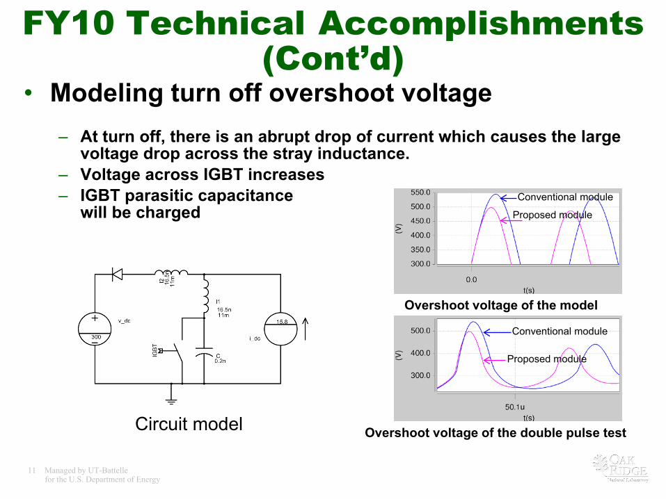
FY10 Technical Accomplishments (Cont’d)
• Modeling turn off overshoot voltage– At turn off, there is an abrupt drop of current which causes the large
voltage drop across the stray inductance.– Voltage across IGBT increases– IGBT parasitic capacitance
will be charged
Circuit model Overshoot voltage of the double pulse test
Proposed module
Conventional module
Conventional module
Proposed module
Overshoot voltage of the model

12 Managed by UT-Battellefor the U.S. Department of Energy
Collaborations
• Partners:– The University of Tennessee (Academic):
Collaborate for development.– MaxQ Technology, LLC (Industry):
Collaborate to fabricate the power module.

13 Managed by UT-Battellefor the U.S. Department of Energy
Future Work – FY10
• Model turn off voltage overshoot and turn on current ringing in a power module with parasitics
• Build a prototype of a 10 kW IGBT single phase leg module using the proposed packaging method
• Measure parasitic inductance and resistance, compare with simulation results

14 Managed by UT-Battellefor the U.S. Department of Energy
Future Work – FY11 and beyond• Build a converter using P-cell and N-cell packaging method to test
and compare the electrical characteristics– Measure and compare voltage spikes across the device– Compare the rise and fall time performance– Calculate the power loss reduction due to the novel package
• Add inductors between P-cell and N-cell to minimize dead-time requirement– Simulation study on inductor value selection– Build an inverter prototype to verify the simulated results– Integrate the inductors into the packaged module
• Model, simulate and build vertical (without wire bond) power module using planar technology and double sided cooling

15 Managed by UT-Battellefor the U.S. Department of Energy
Summary• New packaging method based on P-cell and N-cell is
proposed to reduce the stray inductance between the active switch (IGBT) and diode.
• Electromagnetic and circuit simulation shows reduction of parasitic inductance (20% reduction) and resistance, and corresponding improvement in overshoot voltage in the proposed package module (15% reduction).
• A 10 kW phase leg power module is being developed that incorporates the novel circuit layout.