Non-Contact EEG Active Multielectrode Hardware Design · 2018-02-23 · Non-Contact EEG Active...
149
Non-Contact EEG Active Multielectrode Hardware Design by Scheina Gonzalez Supervised by Professor David Powers School of Computer Science, Engineering, and Mathematics Faculty of Science and Engineering Flinders University This thesis is submitted for the degree of Master of Engineering (Biomedical) 22 May 2017
Transcript of Non-Contact EEG Active Multielectrode Hardware Design · 2018-02-23 · Non-Contact EEG Active...
Non-Contact EEG Active
Multielectrode Hardware Design
by
Scheina Gonzalez
Supervised by
Professor David Powers
School of Computer Science, Engineering, and Mathematics
Faculty of Science and Engineering
Flinders University
This thesis is submitted for the degree of Master of Engineering (Biomedical)
22 May 2017

1 Scheina Gonzalez Non-Contact EEG active Multielectrode Hardware Design
DECLARATION
I certify that this thesis does not incorporate without acknowledgement any material previously
submitted for a degree or diploma in any university; and that to the best of my knowledge and
belief it does not contain any material previously published or written by another person except
where due reference is made in the text.
Scheina Gonzalez
Date: 03/01/2018

Scheina Gonzalez: Non-Contact EEG active Multielectrode Hardware Design 2
ACKNOWLEDGEMENTS
I would like to express my deep gratitude to all those who helped and supported me throughout this
process and made this submission possible.
Firstly, I would like to thank my supervisor Professor David Powers for the opportunity to engage in
this work with him, for his continuous support, motivation, time, and valuable advice. Thank you for
your patience and dedication.
I would also like to thank Craig Peacock, Damian Kleiss and Fiona Cramer from the CSEM
Engineering Service for their continued technical advice.
Editor, Alexander Gosewinckel, provided copyediting and proofreading services, according to the
conditions laid out in the university-endorsed national guidelines 'The editing of research theses by
professional editors'.
Scheina Gonzalez: Non-Contact EEG active Multielectrode Hardware Design 3
Abstract
The electroencephalogram (EEG) is a widely employed method of measuring electrical activity
of the brain for medical diagnosis and research. This electrical activity is generated a few
centimetres below the electrode employed in the measurement. As a result of this, the cortical
current must travel across different resistive levels causing a blurring effect of brain activity at
the scalp. Furthermore, spatial smearing occurs from the necessary use of a reference electrode
to measure the potential difference. An important method utilised to improve EEG spatial
resolution is the surface Laplacian. There are various methods that have been used to improve
EEG poor spatial resolution in the past. The tripolar concentric ring electrode (TCRE), is an
electrode that was developed to improve the surface Laplacian and consequently improve poor
spatial resolution. The first part of this thesis involves the design and assembly of a non-contact
segmented capacitive TCRE. This new design seeks to improve not only the surface Laplacian
and the noise ratio also seeks to increase the communication rate of the EEG and detect and
distinguishing of motor and sensory input from the body. For verification a filter stage was
designed and tested the reliability of the signal acquired. Some problems occurred during the
experiment showing that there was an analogue floating input that affected the signal acquisition.
The second stage of the thesis was dedicated to designing the digitalisation, control, and
communication system of a BCI. To achieve this, the circuits and PCBs of this stage including
AFE and BLE were designed. It was not possible to test this design as time constraints of the
project did not allow for its assembly.

Scheina Gonzalez: Non-Contact EEG active Multielectrode Hardware Design 4
TABLE OF CONTENTS
ABSTRACT ................................................................................................................................................................... 3
LIST OF TABLES ........................................................................................................................................................... 1
LIST OF FIGURES ......................................................................................................................................................... 2
LIST OF ABBREVIATIONS AND SYMBOLS ..................................................................................................................... 4
1. INTRODUCTION .................................................................................................................................................. 5
2. PROJECT BACKGROUND ..................................................................................................................................... 6
2.1. EEG ............................................................................................................................................................ 6
2.2. SIGNAL ACQUISITION AND TYPE OF ELECTRODES ...................................................................................................... 7
2.3. PREVIOUS LITERATURE ...................................................................................................................................... 9
2.3.1. Surface Laplacian in EEG detection ..................................................................................................... 9
2.3.2. Capacitive tilt non-contact electrode design .......................................................................................10
2.3.3. Active non-contact electrode design ..................................................................................................12
3. PROJECT SCOPE .................................................................................................................................................23
3.1. OBJECTIVE ....................................................................................................................................................23
3.2. REQUIREMENTS .............................................................................................................................................23
3.2.1. Procedure and Deliverables ...............................................................................................................23
4. METHODOLOGY ................................................................................................................................................24
5. DESIGN OVERVIEW ............................................................................................................................................25
6. NON-CONTACT ELECTRODE ...............................................................................................................................26
6.1. MATERIAL USE IN ELECTRODES AND THEIR CHEMISTRY .............................................................................................26
6.2. ELECTRODE DESIGN ........................................................................................................................................27
6.3. SHAPE DESIGN...............................................................................................................................................27
6.4. CAPACITANCE ................................................................................................................................................29
6.5. AMPLIFICATION (READOUT CIRCUIT) ...................................................................................................................30
6.5.1. Circuit Design ....................................................................................................................................30
6.5.2. Follower Stage Analysis .....................................................................................................................31
6.5.3. Non-Inverter Stage Analysis ...............................................................................................................31
7. ANALOGUE FRONT ENDS (AFES) FOR BIOPOTENTIAL MEASUREMENTS.............................................................33
7.1. AFES CONCEPT ..............................................................................................................................................33
7.2. AFE SPECIFICATION REQUIREMENT .....................................................................................................................33
7.3. TYPES OF ANALOGUE TO DIGITAL CONVERTERS (ADC) ............................................................................................33
7.3.1. Delta Sigma (ΔƩ)................................................................................................................................34

Scheina Gonzalez: Non-Contact EEG active Multielectrode Hardware Design 5
7.3.2. SARs ..................................................................................................................................................34
7.4. AFE CHOICE .................................................................................................................................................34
7.4.1. ADS129X ...........................................................................................................................................34
8. MICRO CONTROL UNIT (MCU) AND BLUETOOTH LOW ENERGY (BLE) ................................................................37
8.1. MCU CONCEPT .............................................................................................................................................37
8.2. BLE ............................................................................................................................................................37
8.3. MCU/BLE ...................................................................................................................................................37
8.3.1. Dialog Semiconductor .......................................................................................................................38
8.3.1.1. DA14680 ............................................................................................................................................................ 38
8.3.2. Atmel (Arduino) .................................................................................................................................39
8.3.2.1 Arduino Nano (board based on ATmega328) ........................................................................................................ 39
8.4. MCU COMPARISON .......................................................................................................................................40
9. PRINTED CIRCUIT BOARDS (PCBS) LAYOUT DESIGN ...........................................................................................42
9.1. SOFTWARE TOOL ...........................................................................................................................................42
9.2. EEG SENSOR .................................................................................................................................................42
9.2.1. Consideration of the layout ...............................................................................................................42
9.2.1.1. Shielding ...................................................................................................................................................... 42
9.2.1.2. Grounding .................................................................................................................................................... 43
9.3. ANALOGUE FRONT END ...................................................................................................................................43
9.3.1. Layout ...............................................................................................................................................44
9.4. BLE LAYOUT DESIGN.......................................................................................................................................46
9.4.1. Layout ...............................................................................................................................................46
10. SOFTWARE DEVELOPED ................................................................................................................................48
10.1. BLE FIRMWARE .............................................................................................................................................48
10.2. BLE CODE DESIGN ..........................................................................................................................................48
10.3. ELECTRODE TESTING CODE ................................................................................................................................50
11. SAFETY ..........................................................................................................................................................51
12. MEASUREMENT SETUP .................................................................................................................................52
12.1. SETUP .........................................................................................................................................................52
12.2. CAPACITANCE MEASUREMENT...........................................................................................................................53
12.3. FILTER AND AMPLIFICATION CIRCUIT ....................................................................................................................54
12.4. ELECTRODE TEST ............................................................................................................................................56
13. RESULTS AND DISCUSSION ............................................................................................................................57
13.1. ELECTRODE DESIGN .........................................................................................................................................57
13.2. READOUT CIRCUIT ..........................................................................................................................................58
13.3. BAND PASS FILTER AND COMMON MODE CIRCUIT FOR THE TESTING PURPOSE ................................................................59

Scheina Gonzalez: Non-Contact EEG active Multielectrode Hardware Design 6
13.4. PROBLEM CAUSED BY THE POWER LINE ................................................................................................................59
13.5. AFE AND BLE CIRCUIT AND PCB DESIGN ..............................................................................................................60
14. CONCLUSION.................................................................................................................................................63
15. FUTURE WORK AND RECOMMENDATIONS ...................................................................................................64
REFERENCES ..............................................................................................................................................................65
APPENDIX A: GANTT PROJECT PLANER ......................................................................................................................70
APPENDIX B: COMPONENTS LIST ...............................................................................................................................71
APPENDIX C: ELECTRODE SCHEMATIC .......................................................................................................................72
APPENDIX D: READOUT SCHEMATIC ..........................................................................................................................73
D.1. GLOBAL IMPLEMENTATION .....................................................................................................................................73
D.2. ELECTRODE AMPLIFICATION CIRCUIT..........................................................................................................................74
D.3. CENTER ELECTRODE AMPLIFICATION CIRCUIT ...............................................................................................................75
APPENDIX E: LAYOUT SENSOR ...................................................................................................................................76
E.1. READOUT PCB LAYOUT .........................................................................................................................................76
E.2. ELECTRODE PCB LAYOUT........................................................................................................................................77
E.3. 3D ELECTRODE PCB PRINT .....................................................................................................................................78
E.4. READOUT 3D LAYOUT ...........................................................................................................................................79
APPENDIX F: AFE SCHEMATIC ....................................................................................................................................80
F.1. ADS1298 SCHEMATIC CIRCUIT ................................................................................................................................80
F.2. DIGITALIZATION SCHEMATIC CIRCUIT ........................................................................................................................81
APPENDIX G: AFE PCB LAYOUT ..................................................................................................................................82
G.1. 3D TOP PCB PRINT .............................................................................................................................................82
G.2. 3D BOTTOM PCB PRINT .......................................................................................................................................83
G.3. FINAL ARTWORK TOP LAYER PRINT ..........................................................................................................................84
G.4. FINAL ARTWORK BOTTOM LAYER PRINT ....................................................................................................................85
APPENDIX H: BLE SCHEMATIC ....................................................................................................................................86
H.1. DA14680 SCHEMATIC CIRCUIT ..............................................................................................................................86
H.2. COMMUNICATION PCB SCHEMATIC CIRCUIT ...............................................................................................................87
APPENDIX I: CONTROL AND COMMUNICATION PCB ..................................................................................................88
I.1. 3D TOP PCB PRINT ...............................................................................................................................................88
I.2. 3D BOTTOM PCB PRINT .........................................................................................................................................89
I.3. FINAL ARTWORK TOP LAYER ....................................................................................................................................90
I.4. FINAL ARTWORK BOTTOM LAYER ..............................................................................................................................91

Scheina Gonzalez: Non-Contact EEG active Multielectrode Hardware Design 7
APPENDIX J: RISK ASSESSMENT FORMAT ..................................................................................................................92
APPENDIX K: CODE ....................................................................................................................................................93
K.1. FRI BAND PASS FILTER ..........................................................................................................................................93
K.2. BLUETOOTH TESTING .............................................................................................................................................93
K2.1. MATLAB CODE ...................................................................................................................................................93
K2.2. ARDUINO CODE .................................................................................................................................................95
K2.2.1. ADS1298.h .............................................................................................................................................95
K2.2.2 Main code ............................................................................................................................................. 108
K.2.2.3. SPI communication .............................................................................................................................. 110
K.3 SMART SNIPPETS ................................................................................................................................................. 112
K.3.1 ADS.c ...................................................................................................................................................... 112
K3.2 Main.c...................................................................................................................................................... 116
K.3.3 system configuration ............................................................................................................................... 124

1 Scheina Gonzalez Non-Contact EEG active Multielectrode Hardware Design
List of Tables
TABLE 1 - MAIN TYPES OF EEG ELECTRODES [14, 16] ....................................................................................... 8
TABLE 2 - ELECTRODE PERFORMANCE IS EMPLOYING A DIFFERENT MATERIAL FOR COATING [32]............................27
TABLE 3 - DIMENSION, RING SEPARATION, AND CAPACITANCE CALCULATION OF THE ELECTRODE (REFERENCE) .......29
TABLE 4 - PARAMETRIC OF ADS1298 AND ADS1299 [43, 42] ...........................................................................35
TABLE 5 - MCU COMPARISON ........................................................................................................................41
TABLE 6 - OPCODE COMMAND DEFINITIONS [43] ..............................................................................................50
TABLE 8 - CAPACITANCE MEASUREMENT ..........................................................................................................54
TABLE 9 - BUTTERWORTH FILTER SPECIFICATIONS ...........................................................................................55

Scheina Gonzalez: Non-Contact EEG active Multielectrode Hardware Design 2
List of Figures
FIGURE 1 - EXTRACELLULAR TRACES- EEG IMAGE RECORDING [1] ................................................................................................ 7
FIGURE 2 - AMPLITUDE AND FREQUENCY OF THE BIOPOTENTIAL SIGNALS [14]................................................................................. 8
FIGURE 3 - TYPES OF EEG BIOPOTENTIAL ELECTRODES: (A) WET ELECTRODE, (B) DRY ELECTRODE AND (C) NON-CONTACT ELECTRODE [17]. 9
FIGURE 4 - REGULAR PLANE SQUARED GRID WITH INTERPOINT DISTANCE EQUAL TO R USED BY MAKEYEV AND BESIO [2]...........................10
FIGURE 5 - PARAMETER OF THE SEGMENTED COPLANAR SENSOR FINDINGS [20] .............................................................................11
FIGURE 6 - ELECTRODE DESIGN (AUTHOR’S OWN) ...................................................................................................................12
FIGURE 7 - MICRO POWER NON-CONTACT EEG ELECTRODE WITH ACTIVE COMMON-MODE NOISE SUPPRESSION AND CAPACITIVE INPUT
CANCELLATION [25] ................................................................................................................................................13
FIGURE 8 - EEC SIGNAL [25]. ............................................................................................................................................13
FIGURE 9 - SCHEMATIC OF NON-CONTACT ELECTRODE DESIGN [26]. ............................................................................................14
FIGURE 10 - EEG DATA FROM THE 2010 DESIGN [26]. ............................................................................................................14
FIGURE 11 - SECOND EEG SCHEMATIC DEIGN PRESENTED IN 2010 [27] .......................................................................................15
FIGURE 12 - DATA FROM THE ACQUIRED FROM THE ECG EXPERIMENT (RED TRACE OBTAINED USING RED DOT AND THE BLACK SIGNAL OBTAINED
BY USING NON-CONTACT ELECTRODE) [27] ...................................................................................................................16
FIGURE 13 - SCHEMATIC OF THE NON-CONTACT SENSOR FRONT END [28] ....................................................................................17
FIGURE 14 - SAMPLES OBTAINED BY USING STANDARD AG/AGCL (BLUE SIGNAL) AND NON-CONTACT FRONT END (RED SIGNAL) [28]. .........17
FIGURE 15 - CONCEPT AND IMPLANTATION OF USED IN THE COMPACTION DRY EEG ELECTRODE [29] ..................................................18
FIGURE 16 - POWER SPECTRAL OF THE ACQUIRED EEG SIGNAL [29] ............................................................................................19
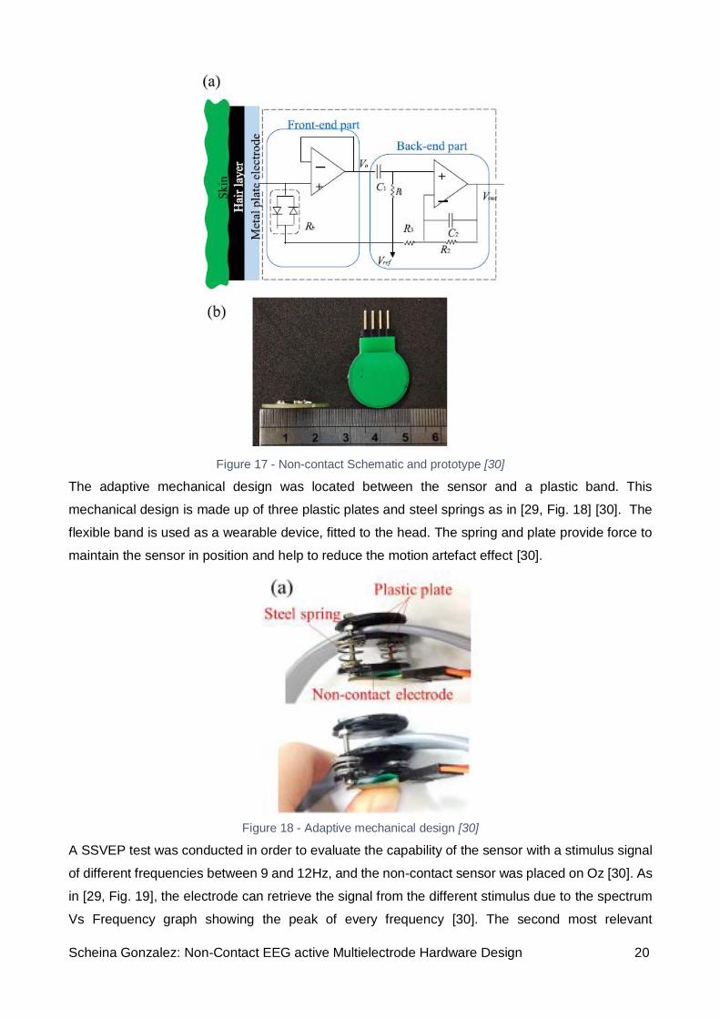
FIGURE 17 - NON-CONTACT SCHEMATIC AND PROTOTYPE [30] ..................................................................................................20
FIGURE 18 - ADAPTIVE MECHANICAL DESIGN [30] ..................................................................................................................20
FIGURE 19 - EEG SIGNAL AND SPECTRA DETECTED BY THE NON-CONTACT SENSOR FOR THE SSVEP EXPERIMENT [30]. .............................21
FIGURE 20 - MEASUREMENT OF EEG UNDER A MOTION ARTEFACT [30] .......................................................................................22
FIGURE 21 - BLOCK DIAGRAM OF NON-CONTACT EEG ACTIVE MULTIELECTRODE HARDWARE DESIGN (AUTHOR’S OWN) ..........................25
FIGURE 22 - CROSS-SECTION OF THE CAPACITIVE ELECTRODE PCB (AUTHOR’S OWN) .......................................................................28
FIGURE 23 - SCHEMATIC OF THE CAPACITIVE ELECTRODE [34] ....................................................................................................29
FIGURE 24 SCHEMATIC CIRCUIT OF THE READOUT AMPLIFICATION CIRCUIT (AUTHOR’S OWN) ............................................................30
FIGURE 25 BUFFER STAGE OF THE READOUT CIRCUIT (AUTHOR’S OWN) ........................................................................................31
FIGURE 26 - GAIN STAGE OF THE READ-OUT CIRCUIT (AUTHOR’S OWN) ........................................................................................32
FIGURE 27- FUNCTIONAL DIAGRAM OF THE ADS1298 AND 1299 [42, 41]. ................................................................................35
FIGURE 28 - DA14680 BLOCK DIAGRAM [46]. .....................................................................................................................39
FIGURE 29 ARDUINO NANO PINOUT [47].............................................................................................................................40
FIGURE 30 - 2D LAYOUT OF THE FINAL READOUT PCB DESIGN FIGURE 31 - 3D PCB LAYOUT (AUTHOR’S OWN) ...............................43
FIGURE 32 - ADS1298 SCHEMATIC CIRCUIT (AUTHOR’S OWN) ..................................................................................................44
FIGURE 33 - TOP LAYER OF THE ANALOGUE TO DIGITAL CONVERTER PCB (AUTHOR’S OWN) ..............................................................44
FIGURE 34 - BOTTOM LAYER OF THE ANALOGUE DIGITAL CONVERTER PCB (AUTHOR’S OWN) ............................................................45
FIGURE 35 - BLE SCHEMATIC CIRCUIT (AUTHOR’S OWN) ..........................................................................................................46
FIGURE 36 BOTTOM LAYER OF THE BLUETOOTH LOW ENERGY MCU AND ANALOGUE TO DIGITAL CONVERTER PCB (AUTHOR’S OWN) .........47

Scheina Gonzalez: Non-Contact EEG active Multielectrode Hardware Design 3
FIGURE 37 - TOP LAYER OF THE BLUETOOTH LOW ENERGY MCU AND ANALOGUE TO DIGITAL CONVERTER PCB (AUTHOR’S OWN) ..............47
FIGURE 38 ADS1298 POWER UP BLOCK DIAGRAM [42] ..........................................................................................................49
FIGURE 39 - SEGMENTED TCRE PROTOTYPE (AUTHOR’S OWN) ..................................................................................................52
FIGURE 40 - SENSOR AND DUMMY ELECTRODE CONNECTED BACK TO BACK (AUTHOR’S OWN) ............................................................53
FIGURE 41 - CAPACITANCE MEASUREMENT (AUTHOR’S OWN)....................................................................................................54
FIGURE 42 - ACTIVE BAND PASS FILTER (AUTHOR’S OWN) .........................................................................................................56
FIGURE 43 - RESULTING ELECTRODE DESIGN (AUTHOR’S OWN) ..................................................................................................57
FIGURE 44 - PCB OF THE READOUT CIRCUIT AND THE ELECTRODE (AUTHOR’S OWN) ........................................................................58
FIGURE 45 - COMMON MODE CIRCUIT (AUTHOR’S OWN) .........................................................................................................59
FIGURE 46 DISTORTED AND ATTENUATED SIGNALS RESULTS .......................................................................................................60

Scheina Gonzalez: Non-Contact EEG active Multielectrode Hardware Design 4
List of Abbreviations and Symbols
Abbreviations
ADC Analogue to Digital Converter
Ag/Agcl Silver / Silver Chloride
AFE Analogue Front Ends
BCI Brain Computer Interface
BLE Bluetooth Low Energy
CC/CV Constant Current / Constant Voltage
CMOS Complementary Metal Oxide semiconductor
CMRR Common mode rejection ration
CREs Concentric ring electrode
DC Direct Current
DSP Digital Signal Processors
DRL Driven right Leg
ECG Electro cardiograph
EEG Electro encephalograph
IDE Integrated developed environment (Arduino)
I/O Input/ output
I2C Inter integrated
MCU Micro Control Unit
MISO Master input Salve output
MOSI Master output slave Input
OTP Open Telecommunication Platform
OP-AMP Operational Amplifier
PCB Printed Circuit Board
SAR Successive Approximation
SC Chip Selection
SCLK Serial Clock
SPE Signal Processing Element
SSVEP Steady State Visual Evoked Potential
SS Slave selection
SPI Serial Peripheral Interface
TCRE Tripolar Concentric Ring Electrode
TGA Therapeutic Goods Administration
UART Universal Asynchronous receiver/Transmitted
ΔƩ Delta-sigma
SYMBOL
OZ EEG POSITION

Scheina Gonzalez: Non-Contact EEG active Multielectrode Hardware Design 5
1. Introduction
An Electroencephalogram (EEG) is a test which measures the electrical activity within a brain [1]. Its
method is non-invasive and its output highly valuable in brain and behaviour research. Therefore
EEG has become a pillar of hospital diagnosis and pre-surgical planning [2, 3].Despite its
advantages, this method is hampered by low spatial resolution, i.e. a selectivity low signal-to-noise
ratio. The low spatial resolution is a result of the blurring effects of the volume conductor with the
plate or disc electrodes [2].
One method to reduce the blurring effect and improve the spatial resolution is surface Laplacian
differentiation, which is the second spatial derivative of the potential distribution on the scalp’s
surface [2]. The surface Laplacian can aid Brain-Computer Interface (BCI) research with at least in
two functions; firstly by working as a spatial filter and reducing spatial noise, and secondly by limiting
the potential sources of the signal [4]. In order to minimise the low spatial frequency and enhance
the spatial selectivity in EEG, one may also employ non-invasive concentric ring electrodes (CREs)
[2]. Moreover, it has been shown that a tripolar CRE (TCRE) can estimate the surface Laplacian
utilising the nine-point method, an extension of the five-point method [2]. A TCRE possesses better
spatial selectivity and signal-to-noise ratio than traditional disc electrodes [2].
The BCI is a system that can be controlled by a subject by using brain signals, which can be used
to help patients with disabilities [5, 6]. EEG is one of the most commonly employed signals in BCI
application since it has a good temporal resolution, can be measured non-invasively and it is
relatively inexpensive [5, 6]. There are numerous types of BCI systems which are based on different
paradigms and methods of EEG collection, one example being the Steady State Visual Evoked
Potential (SSVEP) [5, 6]. The most commonly used BCI systems are based on visual evoked
potentials (VEPs) which are currently the fastest method to set non-invasive BCI control [5, 6]
However, SSVEP is normally for picking up frequencies, while other potentials for spikes, without
depending on spatial localization.
The work presented in this paper has attempted to design capacitive tripolar segmented active
electrodes that can overcome the aforementioned disadvantages of EEG, specifically spatial
resolution and low signal-to-noise ratios. This project also aims to design a system capable of
collecting and transmitting the EEG signal to a computer via Bluetooth for the purpose of
visualisation. The new design seeks to streamline the detection and localisation of motor and
sensory signals down to a few mm; a requirement to distinguish finger movement in the sensory
motor cortex. Currently the detection of fingers in the sensory motor cortex is only be distinguishable
by employing invasive electrodes.

Scheina Gonzalez: Non-Contact EEG active Multielectrode Hardware Design 6
2. PROJECT BACKGROUND
2.1. EEG
The Electroencephalogram (EEG) is the recording of the neural electrical activity within brain
structure from the scalp surface after being collected by a metal electrode. The EEG record is a
spatiotemporal method, and it is a smoothed version of the local field potential (LFP) [7]. The results
are presented in a voltage versus time graph where the y-axis is voltage, and the X axis is time as
is shown in [1, Fig. 1]. The EEG is an entirely non-invasive method that can be conducted on any
patient without having any risk or major discomfort and records information processed by neurons
by means of electrical signals [8, 9]. In the generation of the EEG, the large cortical pyramidal
neurons located in the deep cortical layer play an important role because of the neuron’s orientation
with their apical dendrites, being perpendicular to the cortical surface [9].
The current which is contributed to by the active cellular processes in a specific volume of the brain
tissues is superimposed at a specific area in the extracellular medium, and this generates a potential
in respect to a reference potential, measured in volts (V) [7]. This potential difference generates an
electrical field which is a vector whose amplitude is measured in volts per distance, and it is defined
as the negative spatial gradient of Ve [7]. Ve historically has been assigned to the EEG when this is
recorded from the scalp [7].
The EEG is one of the oldest and most extensively employed methods for brain electrical activity
research. The first EEG recorder was developed by German neuropsychiatrist Hans Berger in 1924,
however, his results were not published until 1929. This report presented a recorded of alpha rhythm
and alpha blocking response of Hans Berger’s son [8, 10]. EEG has since become one of the most
significant contributions to clinical diagnosis and electrophysiology. In a practical medical scenario,
an EEG can allow the determination of relevant clinical parameters such as the location and the
classification of seizures [11, 12]. Thus, a strong correlation exists between the development of EEG
and the classification and understanding of clinical diseases such as encephalopathy and epilepsy.
Additionally, EEG is used for neurofeedback in order to induce long-term changes in the human
corticomotor excitability by employing Brain Computer Interface (BCI), achieved by establishing a
causal link between cortical activity and their function [13].

Scheina Gonzalez: Non-Contact EEG active Multielectrode Hardware Design 7
Figure 1 - Extracellular traces- EEG image recording [1]
2.2. Signal Acquisition and type of electrodes
The EEG signal acquisition is conducted by placing electrodes on the scalp surface in order for the
voltage of the electrodes and the reference to be measured [14]. [14, Fig.2] shows amplitude and
the frequency of the biopotential signal, and as is evident, the maximum amplitude of an EEG signal
is around 1mV, and the maximum frequency is approximately 100Hz [14]. In order to collect a clean
EEG signal, it is necessary to reject or filter the correlating signal such as DC electrode offset voltage
and the noise from the other biopotential signals [14]. Moreover, to obtain a signal at a working level,
it is necessary to add amplification.
The EEG biopotential electrode is a transducer interface between the scalp and the circuit that
converts an ion current to an electric current [14, 15]. The biopotential electrode performance
principle is explained by an electrolyte interface [14, 15]. A chemical reaction occurs at the electrode-
electrolyte interface to enable the current flow between the electrolyte which does not have free
electrons and the electrode that does not have free cations [14, 15]. When the chemical reaction
depends on the concentration of the cations, a charge gradient is formed at the electrode- electrolyte
interface, which result in a potential difference between the interface called half-cell potentials [14,
15].
The EEG biopotential electrodes are classified as being either wet electrodes, dry electrodes, or
non-contact electrodes. The most relevant characteristics of each type of electrode are summarised
in [14, 16, Tab. 1]. A wet electrode is the most common type of electrode employed in biopotential
measurement. This kind of electrode utilises conductive gel for the purpose of acting as an electrolyte

Scheina Gonzalez: Non-Contact EEG active Multielectrode Hardware Design 8
in order to create better contact between the electrode and the scalp [15, 14]. The advantage of wet
electrodes is that they present low motion artefact and low impedance. Despite this, the time of
preparation from the gel smearing and the removal of the gel is problematic [14, 15, 16].
Table 1 - Main types of EEG electrodes [14, 16]
Figure 2 - Amplitude and Frequency of the biopotential signals [14]
Dry electrodes do not need conductive gel to conduct and enhance the electrode-electrolyte
connection [14, 15], therefore the main advantage compared to wet electrodes is the time of
preparation. However due to its leaky capacitive characteristics, this type of electrode requires a
high input impedance readout circuit which should be placed closer to the electrode [14, 15].
Non-contact electrodes are considered to be a pure capacitive electrode [14, 15]. The primary
advantages of this type of electrode are that it can remotely sense the EEG signal, and safety, since
no DC current is drawn from the patient. Additionally, these electrodes are biocompatible [14, 15].
On the other hand, non-contact EEG electrodes require a very high input impedance and is highly
affected by the motion artefact noise [14]. [17, Fig. 3] shows an example of each of the three type
of EEG electrodes: wet (ring), dry and non-contact.

Scheina Gonzalez: Non-Contact EEG active Multielectrode Hardware Design 9
Figure 3 - Types of EEG Biopotential Electrodes: (A) Wet electrode, (B) Dry electrode and (C) Non-contact
electrode [17].
2.3. Previous Literature
2.3.1. Surface Laplacian in EEG detection
Electroencephalography (EEG) is a non-invasive technique and tool employed for several areas of
brain research and hospital diagnoses. Despite its advantages, EEG has a significant disadvantage
caused by its poor spatial resolution. This causes blurring effects of the volume conductor and a
contamination of the signal since reference electrode problems are produced from the absence of
an ideal reference. Nevertheless, some research has been conducted and concludes that the
employment of a concentration ring configuration with an increased inter-ring distance can alleviate
this problem [18, 2].
By employing the surface Laplacian mathematical analysis and Finite element model Makeyev &
Besio demonstrate that increasing the inter-ring distance will provide more accurate Laplacian
estimations and decrease the relative and maximum error [2]. However, a practical demonstration
of the theoretical findings have not yet been presented. Makeyev & Besio employ the (4n + 1)-point
method for to obtain a constant inter-ring electrode distance (n + 1)-polar with n numbers of rings.
This approach is based on the use of distance equal to r and the employment of a plane square as
shown in [2, Fig. 4 ] [2]. Furthermore, the (4n + 1)-point method was modified to obtain the increased
inter-ring distances. The distances between the rings are set r for the first ring, 2r for the second ring,
3r for the third ring, and so on [2].

Scheina Gonzalez: Non-Contact EEG active Multielectrode Hardware Design 10
Figure 4 - Regular plane squared grid with interpoint distance equal to R used by Makeyev and Besio [2].
Extensive investigation into concentric ring electrodes has been conducted in the past, including the
development and testing of a modular active sensor, built using a concentric ring electrode printed
on a flexible substrate [19]. An inner disc forms the electrode design, and two concentric ring
electrodes which are placed in a bipolar configuration. However, the design was only tested by
recording an Electrocardiograph (ECG) signal. Prats et al. found that the flexible electrode showed
better performance than rigid electrodes since the flexible electrode presented higher skin-electrode
contact. Unfortunately this experiment has only been conducted in the collection of ECG signals
which are larger than EEG signals, for which the reliability of collection remains relatively unknown.
2.3.2. Capacitive tilt non-contact electrode design
Guo et al. (2016) have also studied the concentric coplanar electrodes, however, unlike Makeyev &
Besio, segmented electrodes were used and employed as a capacitive tilt sensor [20]. Guo et al. as
Makeyev & Besio, focus on developing the mathematical model by connecting the geometric
dimensions to sensor capacitance, the model expressions obtained by employing the Hankel
transformation to solve the Laplacian equations. Additionally, Guo et al. employ the Finite element
model to evaluate and verify the reliability of the findings [20]. The analytical model of the segmented
coplanar sensor was proposed by using two concentric electrodes that have a central angle, and
inner and outer radii for the inner and outer ring or segmented electrode as is shown in Figure 5 [20].
For the mathematical model, it was assumed that permittivity of the medium is ε and the thickness
of the medium is h. Furthermore, it is assumed that the Laplacian equation ∆𝜙 = 0 is satisfied by the
potential in the medium. The mathematical and theoretical definition of capacitance can be
expressed as in [20, Eq.1]. Guo et al. used this equation to evaluate the mathematical model by
employing Finite Element (FE). The results of their research showed that the capacitance of the
annular coplanar sensor is linearly proportional to the medium permittivity and the central angle, and
the inner annular ring should be wider than the outer annular ring.

Scheina Gonzalez: Non-Contact EEG active Multielectrode Hardware Design 11
Equation 1 analytical calculation of the capacitance [20]
Figure 5 - Parameter of the segmented coplanar sensor findings [20]
As we can see, many researchers have mathematically demonstrated the reliability of the coplanar
concentric sensor to be used for a different purpose, especially in biosignals such as ECG and EEG.
Nevertheless, a segmented coplanar which has shown similar mathematical results such as the
distance between rings and the width of the ring have been not employed in the collection of bio
signals. Therefore one of the primary objectives of this thesis is to build a segmented coplanar ring
capacitive electrode with an increase in the ring separation to be used in the collection of EEG signal
with the finality to obtain reliable signals that can be used in future research and hospital diagnose
as is shown in [20, Fig. 5]. The electrode designed will be an active non-contact capacitive electrode,
and the segmentation will act as an individual electrode and as a grid. The segmentations,
organisation and dimension of the rings seek to overcome the disadvantage of poor spatial resolution
highlighted by previous research. The implementation of the grid in the electrode design is the result
of research showing that a grid electrode design can reduce the motion artefact noise, such as
conducted by Peng et al. and Wartzek et al.

Scheina Gonzalez: Non-Contact EEG active Multielectrode Hardware Design 12
Figure 6 - Electrode design (Author’s own)
Peng et al. present in their publication a design of an active drive shielding electrode with a grid-
multilayer; this design was then compared with a different electrode design. This particular
experiment shows that the motion artefact and the effects of the signals interferences are lower in
comparison with other electrodes that were evaluated [21]. Furthermore, Wartzek, et al. state that
an appropriate electrode-body design can reduce motion artefacts, while the use of a grid electrode
can help to reduce accumulation charges [22].
2.3.3. Active non-contact electrode design
To obtain design and build an EEG sensor which delivers a reliable signal, a good electrode design
is not solely sufficient. It is also necessary to have an efficient electronic design of the stage of
amplification, control, and transmission of the signal. Designing a reliable amplification stage is
crucial, since EEG signals are very weak at approximately less than 100µV at 100Hz, causing
measurement difficulties. Sullivan et al. design a low-noise non-contact EEG/ ECG sensor; the low-
noise capability was achieved by having an active shield [23].
The circuit design presented by Sullivan et al. employs an instrumentation amplifier due to the low
input bias current, typically 3fA. Despite the low current, they decide to implement a reset circuit
which includes two transistors and two resistors for the purpose of avoiding high impedances in the
input node towards one of the supply rails [23]. The research conducted by Sullivan et al. has
allowed the door or new possibilities in the design of integrated non-contact EEG sensors, since it
was operational from up to 3mm from the skin. In addition to achieving low noise, another aspect to
be considered in the design of a non-contact capacitive sensor is power consumption and the
creation of sensor networking. Chi et al. implemented these considerations in the design of a non-
contact EEG/ECG sensor [24, 25].
The Chi et al. design consisted of two boards. The first board constitutes of the electrode or sensing
plate, the bottom layer of the printed Circuit Board (PCB), and the amplification stage which includes

Scheina Gonzalez: Non-Contact EEG active Multielectrode Hardware Design 13
the capacitive cancellation front end and the differential gain stage. The amplification stage is located
in the top layer of the PCB. The second board consists of the analogue to digital converter (ADC)
and the data interface, as shown in [25, Fig. 7]. As shown, the gain of the front-end amplification
provides impedance conversion and signal gain to the sensor, which was set by the resistors R1 and
R2. Furthermore, to ensure the capacitive cancellation and avoid the banding of the gain, the
capacitance of the capacitor C1 should be large and the capacitance of the capacitor Cs should
lowered [25, 24].
Figure 7 - Micro power Non-contact EEG Electrode with Active Common-Mode Noise suppression and
capacitive input cancellation [25]
Therefore, it is possible to state that sensor electrode sensitivity, noise levels and channel matching
have a high dependence on the front-end stage presented. With this electrode design Chi et al. was
able to conclude that by adding the capacitive cancellation circuit, it is possible to eliminate the
variations in the gain and the channel mismatch [24, 25]. However as we can see in [25, Fig. 8], the
data obtained from the experiment carried out during the sensor test shows that the noise from
motion artefact is not entirely cancelled, resulting in an ECC signal that is not completely reliable
[24, 25].
Figure 8 - EEC signal [25].
Tests conducted by Chi et al. show some promising results, such as the possibility of implementing
a small networking of active capacitive electrode. Further research in 2010 resulted in two new

Scheina Gonzalez: Non-Contact EEG active Multielectrode Hardware Design 14
design of Non-contact EEG/ECG Electrodes for Body Sensor Networks. In this case both designs
were wireless systems. The wireless bio-potential instrumentation system designs by Chi, et al.
consist of a non-contact capacitive electrode that can function without a direct skin connect.
The first design shown in Figure 9 is unlike the designs presented in 2009 as it comprises of an ultra-
high impedance front end implemented using an INA116, and a LTC6078 for the differential gain
amplification [26]. In the ultra-high impedance front end, a low pass version of the input to remove
the drift and DC offset was used. This low pass version of the input was obtained from the non-
inverting input and connected to the output. This produced an AC coupling without affecting the input
impedance. Also, to maximise the signal swing the output was centred in the mid-rail.
Figure 9 - Schematic of non-contact electrode design [26].
Even though this circuit design had a stronger focus on noise correction, few improvements were
made as the noise is not entirely removed and the system is still not completely reliable, as evident
in [25, Fig. 10]. The signal is in fact noisier than the one shown in [25, Fig 8]. Further research and
design improvements are required to improve the reliability, sensitivity, and noise level of this design.
Figure 10 - EEG data from the 2010 design [26].
The second design presented in 2010 is shown in [26, Fig. 11]. This is a simpler, replicable and
inexpensive design in contrast with the design presented in previous works [27]. As in [26, Fig. 11],
the design includes two buffers and a high pass filter stage in the electrode section. The gain stage
is formed by a differential amplification stage and low pass filter stage. This design also has a
capacitive DRL (drive right leg) electrode with an amplification stage used to reduce the common
mode interference [27].

Scheina Gonzalez: Non-Contact EEG active Multielectrode Hardware Design 15
Figure 11 - second EEG schematic deign presented in 2010 [27]
In contrast to previous papers, reference to the subject grounding were utilised due to its necessity
in achieving good signal quality [27]. As in [26, Fig. 11], this design employed a capacitive coupling
to connect the circuit back to the body, and was implemented using a dummy electrode without
components [27]. This method reduces common mode interferences. In addition, the signal obtained
by employing this design is clearer than the signal collected by using previous sensor designs due
to the combination of the use a battery power system and active ground [27]. However, the result
showed that the system is highly sensitive to motion artefacts. As we can see in the results shown
in [26, Fig. 12] obtained from the ECG experiments, the signal that shows more sensitivity to motion
artefacts is the signal collected using the non-contact electrode [27]. In conclusion, this device still
needs improvement the electrode sensitivity to motion artefact and friction to be able to be used in
medical grade applications [27].

Scheina Gonzalez: Non-Contact EEG active Multielectrode Hardware Design 16
Figure 12 - Data from the acquired from the ECG experiment (red trace obtained using red dot and the black
signal obtained by using Non-contact electrode) [27]
The previous implementation by Chi, et al. used discrete off the shelf amplifiers. The use of this
technology presented some disadvantages due to the necessity of tuning input capacitance
neutralisation networks manually, while also requiring a complex DC-bias circuit [28]. This led to Chi
et al. designing and fabricating a new front end sensor circuit with a custom high input impedance
with low noise [28]. The new circuit has an amplifier fully bootstrapped to avoid the use of a capacitive
neutralisation circuit. Moreover, it includes an on-chip biasing networking with the purpose to
guarantee DC stability and prevent the need for high resistances [28]. [27, Fig. 13] shows the
schematic of the front end circuit. The unit gain amplifier in the circuit has functionality, firstly by
bootstrapping the parasitic input impedances, and it also maintains a constant voltage across them.
The shield is driven by the output of the unity gain amplifier which encloses the trace of the unity
gain amplifier input.

Scheina Gonzalez: Non-Contact EEG active Multielectrode Hardware Design 17
Figure 13 - Schematic of the Non-contact sensor front end [28]
To demonstrate the reliability of the new front end sensor circuit, an ECG experiment was conducted
where it contrasted the signal obtained by using the non-contact electrode and signal collected by
employing an Ag/AgCl electrode [28]. As in [27, Fig. 14], the signal collected by using the new non-
contact electrode design is slightly more stable than the previous design [28]. However, the signal
presents more noise than the design presented in 2010, shown in [26, Fig. 12].
Figure 14 - samples obtained by using standard Ag/AgCl (blue signal) and Non-contact front end (Red signal)
[28].
The new design presented has improvements that allow this circuit to perform slightly better than
previous iterations [28]. However it is possible to build higher non-contact electrodes that are much
simpler and without the requirement of a big adjustment. Dry and Non-contact EEG electrodes, which
do not require direct skin contact or even conductive gel, could be considered as part and enable a
brain-computer interface to be used in research and even in clinical diagnosis. Chi et al. decided to
conduct an experiment comparing their latest EEG electrode, their dry electrode design, and a typical
Ag/AgCl wet electrode within a steady visual evoked potential (SSVEP) BCI (Brain-computer

Scheina Gonzalez: Non-Contact EEG active Multielectrode Hardware Design 18
Interface) paradigm [29]. The dry electrode design employ consisted of two parts as in [28, Fig. 15].
The bottom section is formed by spring loaded fingered contact posts that can penetrate the hair and
make skin contact without preparation, whereas the top section consists of active buffering circuitry
with an off the shelf CMOS-input Operational Amplifier (Op-Amp) [29].
Figure 15 - concept and implantation of used in the compaction Dry EEG electrode [29]
The experiment that was conducted required each subject to guess a single SSVEP target stimulus,
displayed on a CRT monitor at 10 Hz for a 1-min duration [29]. Throughout the experiment, a signal
from the SSVEP was decoded with the aim of verifying the presence of the stimulus signal [29]. To
obtain the best possible dataset, the experiment was conducted three times. The result showed that
the electrodes are capable of acquiring an ECG signal due to the signal stimulus being clearly visible
for all electrodes as in [28, Fig. 16]. It is also evident that the amplitude of the SSVEP and noise
depend on the subject [29]. Moreover, it is noted that the non-contact electrode exhibited a higher
amount of low-frequency drift and broadband noise than the dry electrode. The disadvantages
observed for the non-contact electrode are unlike the dry electrode due to the high coupling
impedance and upper sensitivity to motion artefacts [29]. The experiment also found that unlike the
wet electrode, the dry and non-contact electrodes required more time to reach a stable trace [29].
Moreover, they also observed that the signal acquired with dry and non-contact electrodes do not
show degradation over time [29].

Scheina Gonzalez: Non-Contact EEG active Multielectrode Hardware Design 19
Figure 16 - Power Spectral of the acquired EEG signal from subjects 1, 2, 8 and 10 [29]
It is therefore possible to conclude that the non-contact electrodes and the BCI requires greater
improvement and care with the design, specifically a non-contact sensor to overcome the EEG level
signal problems [29]. Furthermore, the dry and non-contact electrodes can be successfully employed
within controlled BCI application [29].
More recent research on non-contact electrodes is offered by Chen et al., presenting a new non-
contact EEG electrode design With Adaptive Mechanical Design for Measuring EEG in a Hairy Site
[30]. The adaptive mechanical design was conceived with the goal of improving the motion artefact
effect. The non-contact sensor design is formed by two parts as in [29, Fig. 17]. The bottom part
forms the electrode with a circular copper film, while the top part amplification state consists of the
front-end section and back-end section. As in [29, Fig. 17], the front-end of the circuit involves a
unitary gain amplifier employed to provide a high input impedance and antiparallel diodes used to
avoid use signal attenuation [30]. The back-end of the circuit is a band-pass filter used remove the
high-frequency noise and the motion artefact effect [30].
Scheina Gonzalez: Non-Contact EEG active Multielectrode Hardware Design 20
Figure 17 - Non-contact Schematic and prototype [30]
The adaptive mechanical design was located between the sensor and a plastic band. This
mechanical design is made up of three plastic plates and steel springs as in [29, Fig. 18] [30]. The
flexible band is used as a wearable device, fitted to the head. The spring and plate provide force to
maintain the sensor in position and help to reduce the motion artefact effect [30].
Figure 18 - Adaptive mechanical design [30]
A SSVEP test was conducted in order to evaluate the capability of the sensor with a stimulus signal
of different frequencies between 9 and 12Hz, and the non-contact sensor was placed on Oz [30]. As
in [29, Fig. 19], the electrode can retrieve the signal from the different stimulus due to the spectrum
Vs Frequency graph showing the peak of every frequency [30]. The second most relevant

Scheina Gonzalez: Non-Contact EEG active Multielectrode Hardware Design 21
experiment was an EEG measurement under motion artefacts [30]. To clearly observe sensor
performance and the mechanical design under motion artefacts, Che et al. placed two pairs of the
non-contact sensor on a subject around the Oz location, with and without the mechanical design to
acquire EEG signals under different motion conditions [30]. The result of this experiment shows a
slight improvement of the signal by employing the adaptive mechanical design. As is presented in
[29, Fig. 20], the differences between with and without the adaptive mechanical design is more
clearly observed during heavy motion [30]. It is therefore possible to conclude that the adaptive
mechanical design minimises the motion artefact effect [30], while simpler designs can prove to
provide better results. On the other hand, this design still required improvement in sensibility and
reliability [30].
Figure 19 - EEG signal and spectra detected by the non-contact sensor for the SSVEP experiment [30].

Scheina Gonzalez: Non-Contact EEG active Multielectrode Hardware Design 22
Figure 20 - Measurement of EEG under a motion artefact [30]
The non-contact sensors presented showed improvements in their circuit design and therefore an
improvement in performance for implementation time, signal collection, and signal reliability.
However the electrodes used in each design were of the same circular copper plate which may be
the cause of the persistent noise issues. It was also possible to observe that almost all front end
designs were overly complex, causing an increase to the size of the front stage. It is possible that
the circuit required does not need to be so complex and may allow for a smaller front stage.

23 Scheina Gonzalez Non-Contact EEG active Multielectrode Hardware Design
3. Project Scope
3.1. Objective
This thesis aims to design a non-contact active capacitive EEG electrode which improves the
accuracy of the Laplacian estimation. The goal of this new electrode design is to improve the
recording of brain signals by improving noise performance (artefact rejection) and therefore obtaining
a more reliable signal for clinic diagnosis and future research examining the possibility of detecting
and isolating motor and sensory inputs from the body. This project designs and develops an active
non-contact segmented coplanar ring capacitive electrode. The BCI system measure and transmits
the EEG signal via Bluetooth. This new model incorporates design elements such as multiple signals
from the same area, portability, and wireless bio-signal recording.
The tripolar concentering ring electrode (TCRE) mathematically proven in [2] will be improved using
a segmented variation. The electrode design will be powered by a single rechargeable coin cell
battery in each sensor, and rechargeable by using a BLE chip feature. The non-contact EEG active
Multielectrode prototype will record a reliable EEG signal, and with a BCI system, transmit the EEG
signal via Bluetooth. The electrode design incorporates the idea of a tripolar concentering ring
electrode (TCRE) to take advantage its ability to automatically achieve the surface Laplacian.
Additionally, the TCRE obtains a bipolar difference of the surface potential from the rings that form
the electrode [2, 31]. The new EEG electrode will contribute to, and be the base of, a new design
and research aiming to improve non-invasive EEG signal collection.
3.2. Requirements
The criteria that should be utilised in order to guarantee the success of the prototype device are:
The device is portable and battery powered;
The electrode is an active and capacitive (not requiring conductive gel);
Wireless bio-signal recording networking/BCI;
Setup time of the device is less than conventional electrodes;
The device detects and distinguishes motor and sensory inputs from the body;
The electrode design provides artefact attenuation; and
The electrode design improves the accuracy Laplacian estimation.
3.2.1. Procedure and Deliverables
To be able to complete the project on time and fulfil the stated requirements, a Gantt chart shown
under Appendix A was designed, stating the deliverables and the time that each deliverable will take.
The main deliverables consist of an electrode design and its amplification stage, the analogue to
digital PCBs, Bluetooth hardware, and the software design.

Scheina Gonzalez: Non-Contact EEG active Multielectrode Hardware Design 24
4. Methodology
The thesis first conducted a literature review on EEG, how it is measured, the type of electrodes
commonly used and the previous research. The literature related to EEG is already extensive and
therefore is a well-documented field of research. After having conducted the literature review and
collating the necessary information, the focus changed the technical aspect of the project, such as
the design to be used, suitability of components, and the technical information to be employed in the
development of the thesis.
The first stage of the hardware design involved deciding which type of electrode is most appropriate,
how it will be built, its capabilities, and its limitations. After deciding upon the type of electrode design
and during the initial design phase, the complete system design was developed taking into
consideration the hardware components available on the market. The hardware selection and design
were modified due to the availability of new BLEs with more features such a size decrease and
charging option. The selection of the actual components and the system design was based on
technical documentation of the components and previews works.
The second stage of the hardware design was the development of the amplification stage for the
electrodes, the front-end, and traditional circuits. After completing the initial circuit designs, they were
presented to, and discussed with, supervisor Professor Powers and met his approval, allowing the
design of the PCB to continue.
After obtaining approval of the circuit design, the PCBs were developed while the BLE was being
programmed. A few iterations of the PCB’s design were developed during the process. This was
conducted so that focus was on one section at a time, and that each completed stage was integrated,
such as the electrode and its readout circuit. The approach was focussed primarily to the electrode
design and its build. Due to time and budgetary constraints, the ADC and BLE were designed only,
and are in the process of being assembled.

25 Scheina Gonzalez Non-Contact EEG active Multielectrode Hardware Design
5. Design Overview
To show a better and clearer view of the whole system, a design overview is presented to give a
perspective of the prototype development and a see how it may operate after completion. From the
project scope, it is possible to derive three major design sections which required development: the
electrode, the front-end, and the output system.
Fig. 21 presents a block diagram of the main elements of the last electrode of the EEG device
prototype which permits the EEG device to operate and perform its functions satisfactorily. The
system design constitutes of six heptrodes on an SPI bus feeding one MCU/BLE.The signal is
acquired from the scalp of the subject by employing the new EEG electrode designed to the
amplification stage, and to the ADC also knows as Analogue Front End (AFE). The ADC or AFE
quantises the signal acquired to be transmitted through a BLE system via Bluetooth to a computer.
A complete list of the components used in the EEG device prototype can be found in Appendix B.
Figure 21 - Block diagram of non-contact EEG active Multielectrode Hardware Design (Author’s own)
Electrode
ADC
MCU/BLE
PC
RLD
RLD Battery
Power
Battery
Power
Electrod Amplification
Electrode
ADC
MCU/BLE
Electrod Amplification
Common mode from
neighboured
Common mode from
Mastoid
Common mode from
Mastoid
One BLE per chain of
6 electrodes
26 Scheina Gonzalez Non-Contact EEG active Multielectrode Hardware Design
6. NON-CONTACT ELECTRODE
Conventional wet (gel) and dry electrodes are widely employed for biopotential measurements such
ECG and EEG, despite their disadvantages such as long preparation time, discomfort, pain, and skin
irritation. The work presented in the paper consists of the design and development of a non-contact
capacitive electrode prototype for EEG signal collection which does not suffer from these
disadvantages. The new electrode design concept lies between the variable inter-ring distance
concentric ring electrode [2], and a segment annular coplanar capacitive tilt sensor [20], allowing the
advantages of both to be utilised and addressing most of the disadvantages. The new electrode
design is a segmented tripolar capacitive electrode.This non-contact electrode would improve the
accuracy of the Laplacian estimation, provide artefact attenuation, and detect and distinguish motor
and sensory inputs from the body. In addition, this design enhances the spatial resolution of this type
of electrode via an increase in the ring separation, while the ring is a smaller diameter (inner ring
9.6mm, second ring 15.8 mm and external ring 20.4 mm) compared to previous non-contact active
electrodes (22.5mm to 24.26mm). One of the most relevant characteristics of non-contact electrodes
is their ability to act as a capacitor between the body and the readout interface, allowing for remote
sensing (without direct skin or scalp contact) [14]. Furthermore, the readout circuit should be located
near to the electrode.
6.1. Material use in electrodes and their Chemistry
One key factor that should be considered when attempting to obtain a reliable signal from an EEG
electrode is the electrochemical properties of the materials employed in the electrode construction
and coating that is used [32]. This can significantly affect the quality of the EEG measurement [32].
Additionally, the knowledge of the interaction between the electrode-electrolyte interfaces is
fundamental for the development of the electrode and the analysis of its performance [32]. Since the
non-contact electrode, like the dry electrode, does not require conductive gel, the material employed
on the surface of the electrode dictates performance in respect to contact impedance and noise [32].
The recording of low-frequency components is particularly challenging due to contamination by noise
and drift in the half-cell potential [32]. [31, Tab. 2] shows a summary of different possible materials
and their respective performance. Silver/silver chloride (Ag/AgCl), silver, and gold are shown to offer
the best performance to employ in an EEG electrode [32]. The plate electrode is the most commonly
used electrode in non-contact EEG design. To our knowledge, tripolar concentric ring electrodes
(TCRE) and tilt electrodes have not yet been utilised and considered in non-contact EEG recording.

Scheina Gonzalez: Non-Contact EEG active Multielectrode Hardware Design 27
Table 2 - Electrode performance is employing a different material for coating [32].
6.2. Electrode Design
This design attempts to overcome the clear disadvantages associated with common electrodes and
non-contact electrodes such as poor accuracy for Laplacian estimation, long setup time, and low
artefact noise reflection. This design is based on the mathematics developed in [2] and [20]. Both
papers present similar ideas on electrode performance improvements by varying the distance of the
concentric rings. However, the mathematical proof developed is quite different to each other, as
detailed in Section 2.
The design presented here considers a concentric ring electrode configuration with the variable inter-
ring distance that increases linearly from the central disc, as the concentric ring electrodes are
theorised to provide a more accurate and reliable surface Laplacian estimation relative to constant
inter-ring distances alternatives. The segmentations on the electrodes rings are implemented into
the design with the intent to increase the communication rate of the EEG, obtain multiple signals
from the same electrode area, provide greater artefact attenuation and attempt to detect and
distinguish the motor and sensory inputs from the body.
6.3. Shape Design
The capacitive electrode was built as a parallel layer, four metallic layers separated by dielectric
material and two ground layers. Both layers were composed of the metal layer on a PCB and the
scalp of the patient. The previous setup described is shown in [Fig. 22]. The capacitance of the
parallel-plate capacitor is defined in [ [33], EQ. 2] where A is the area of the plate, D is the separation
between the plates, εr is the relative static permittivity, and ε0 is the permittivity of the free space.
𝐶 =𝜀𝑟𝜀0𝐴
𝐷
Equation 2 Capacitance [33].
In this type of capacitor, two of the variables vary with the location of the electrode on the surface of
the subject body, the separation between the electrode and the skin and the dielectric relative static
permittivity, making it difficult to obtain the precise value of the capacitance of the electrode. Many
constants form the dielectric relative static permittivity such as the solder mask, the hair, and the
sweat on the skin.
Scheina Gonzalez: Non-Contact EEG active Multielectrode Hardware Design 28
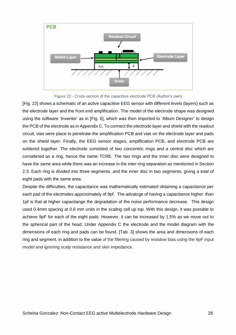
Figure 22 - Cross-section of the capacitive electrode PCB (Author’s own)
[Fig. 22] shows a schematic of an active capacitive EEG sensor with different levels (layers) such as
the electrode layer and the front end amplification. The model of the electrode shape was designed
using the software ‘Inventor’ as in [Fig. 6], which was then imported to ‘Altium Designer’ to design
the PCB of the electrode as in Appendix C. To connect the electrode layer and shield with the readout
circuit, vias were place to penetrate the amplification PCB and vias on the electrode layer and pads
on the shield layer. Finally, the EEG sensor stages, amplification PCB, and electrode PCB are
soldered together. The electrode consisted of two concentric rings and a central disc which are
considered as a ring, hence the name TCRE. The two rings and the inner disc were designed to
have the same area while there was an increase in the inter-ring separation as mentioned in Section
2.3. Each ring is divided into three segments, and the inner disc in two segments, giving a total of
eight pads with the same area.
Despite the difficulties, the capacitance was mathematically estimated obtaining a capacitance per
each pad of the electrodes approximately of 9pf. The advatcge of having a capacitance higher than
1pf is that at higher capacitange the degradation of the noise performance decrease. This design
used 0.4mm spacing at 0.6 mm units in the scaling cell up top. With this design, it was possible to
achieve 9pF for each of the eight pads. However, it can be increased by 1.5% as we move out to
the spherical part of the head. Under Appendix C the electrode and the model diagram with the
dimensions of each ring and pads can be found. [Tab. 3] shows the area and dimensions of each
ring and segment, in addition to the value of the filtering caused by resistive bias using the 9pF input
model and ignoring scalp resistance and skin impedance.

Scheina Gonzalez: Non-Contact EEG active Multielectrode Hardware Design 29
Table 3 - Dimension, ring separation, and capacitance calculation of the electrode (Author’s own)
6.4. Capacitance
This section presents the circuit theory behind of the capacitive electrode; the aim is to create a
capacitance between the surface of the scalp or skin and the readout circuit with the finality of
collecting the biopotential signal generated by the body. The capacitive electrode acts as a high pass
filter due to the capacitor create high impedance to DC voltage with input Residence. The circuit
schematic of the capacitive electrode if shown in [34, Fig. 23].
Figure 23 - Schematic of the capacitive electrode [34]
The Cin on the circuit shown in [34, Fig. 23] refers to the capacitance seen in op-amp output, the Zi
is the input resistance of the Op-amp, and the Csensor is the capacitance of the electrode. By
conducting an AC, the analysis was obtained the transfer function of the circuit as shown below
showing the high-pass filter nature.
Vout (s) =Zi ∥
1sCin
1sCsensor
+ (Zi ∥1
sCin)
∗ Vskin(s)
Equation 3 Voltage output of the electrode [35].
Applying some algebra was obtained that the transfer function of the electrode is:
H(s) =Vout (s)
Vskin(s)=
Csensor
Csensor + Cin∗
s
s + w0
Equation 4 - Transfer function of the electrode [35].
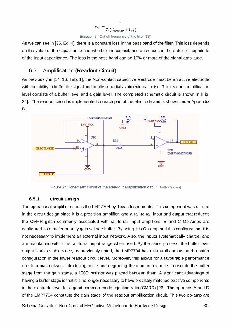
Scheina Gonzalez: Non-Contact EEG active Multielectrode Hardware Design 30
w0 =1
Zi(Csensor + Cin)
Equation 5 - Cut-off frequency of the filter [35].
As we can see in [35, Eq. 4], there is a constant loss in the pass band of the filter. This loss depends
on the value of the capacitance and whether the capacitance decreases in the order of magnitude
of the input capacitance. The loss in the pass band can be 10% or more of the signal amplitude.
6.5. Amplification (Readout Circuit)
As previously in [14, 16, Tab. 1], the Non-contact capacitive electrode must be an active electrode
with the ability to buffer the signal and totally or partial avoid external noise. The readout amplification
level consists of a buffer level and a gain level. The completed schematic circuit is shown in [Fig.
24]. The readout circuit is implemented on each pad of the electrode and is shown under Appendix
D.
Figure 24 Schematic circuit of the Readout amplification circuit (Author’s own)
6.5.1. Circuit Design
The operational amplifier used is the LMP7704 by Texas Instruments. This component was utilised
in the circuit design since it is a precision amplifier, and a rail-to-rail input and output that reduces
the CMRR glitch commonly associated with rail-to-rail input amplifiers. B and C Op-Amps are
configured as a buffer or unity gain voltage buffer. By using this Op-amp and this configuration, it is
not necessary to implement an external input network. Also, the inputs systematically charge, and
are maintained within the rail-to-rail input range when used. By the same process, the buffer level
output is also stable since, as previously noted, the LMP7704 has rail-to-rail outputs, and a buffer
configuration in the lower readout circuit level. Moreover, this allows for a favourable performance
due to a bias network introducing noise and degrading the input impedance. To isolate the buffer
stage from the gain stage, a 100Ω resistor was placed between them. A significant advantage of
having a buffer stage is that it is no longer necessary to have precisely matched passive components
in the electrode level for a good common-mode rejection ratio (CMRR) [26]. The op-amps A and D
of the LMP7704 constitute the gain stage of the readout amplification circuit. This two op-amp are

Scheina Gonzalez: Non-Contact EEG active Multielectrode Hardware Design 31
configured as non-inverters as is shown in [Fig 24]. The circuit was set with a gain of 21, while the
analysis of this circuit is shown in section 6.4.2.
6.5.2. Follower Stage Analysis
As in [Fig25], the circuit is a unity gain amplifier or follower. Since the input signal V1 is found at the
positive input of the Op-amp, and the rule states that “when the op-amp output is in the linear range,
the two input terminals are the same voltage” [15], Vi must be seen at the negative input. Output Vo
of the op-amp is also connected to the negative input and the output is therefore equal to the input
(Vo=Vi), or the output follows the input.
Figure 25 Buffer stage of the readout circuit (Author’s own)
6.5.3. Non-Inverter Stage Analysis
As in [Fig. 26], the circuit is a non-inverter operational amplifier with a gain of 21. To analyse this
circuit and show how the gain was obtained, it is necessary to use the two basic rules for the design
of op-amps circuits:
1. “when the op-amp output is in the linear range, the two input terminals are the same voltage”
[15].
2. “no current flow into either input terminal of the Op-amp” [15].
𝑉12 = 𝑉13
Equation 6 - Op-amp rule 1 [15]
V12 appears at the negative input V13 of the op-amp. This cause current i shown in [Eq. 7]. To follow
the ground, the current i cannot come from the negative input of the circuit. Therefore, the current i
must flow through the resistance R11. Now it possible to calculate Vo as is shown in Equation 8 and
solve for the gain as shown in Equation 9.
i =V13
R10⁄
Equation 7 - Current i
Vo = i(R11 + R10)
Equation 8 - Output Voltage Vo
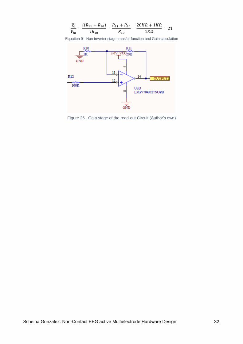
Scheina Gonzalez: Non-Contact EEG active Multielectrode Hardware Design 32
𝑉𝑜
𝑉𝑖𝑛=
𝑖(𝑅11 + 𝑅10)
𝑖𝑅10=
𝑅11 + 𝑅10
𝑅10=
20𝐾Ω + 1𝐾Ω
1𝐾Ω= 21
Equation 9 - Non-inverter stage transfer function and Gain calculation
Figure 26 - Gain stage of the read-out Circuit (Author’s own)

33 Scheina Gonzalez Non-Contact EEG active Multielectrode Hardware Design
7. Analogue Front Ends (AFEs) for Biopotential Measurements
For an efficient and reliable interconnection between the sensor stage and the microcontroller stage
of a circuit design, it is necessary to have an intermediate stage which allows for a conversion of the
analogical signal obtained by the sensor into a digital signal [36]. In addition, this intermediate stage
should be able to condition and filter the signal to remove noise and add amplification to weak signals
such as physiological signals [36]. This chapter presents a brief discussion of the concept of the
analogue front end and its applicability to this work.
7.1. AFEs concept
The AFE is comprised of analogue signal conditioning circuits combining amplification, filtering, and
in some cases a specific application for sensors [36, 37, 38]. This device can perform many functions,
strictly depending on the application for which is used. For example in this work, the AFE was
employed to condition the EEG analogue signal to be later transformed into its digital representation.
The AFE can be connected directly to a microcontroller or microprocessor by a standard serial
communication. Another important feature of AFE is scalability as it has enough ports to be able to
connect multiple sensors reduce the size of the circuit board, decrease the component require and
improve the power consumption [36, 37, 38].
7.2. AFE specification requirement
To select the appropriate AFE component for the EEG signal acquisition, it was necessary to set
some requirements to refine the options. During the research conducted to find the most suitable
AFE for an EEG signal, only two components were found, the ADS1298 and ADS1299, offered the
best alternative and flexibility that satisfied the following requirements conditions:
High scalability
o Minimum eight differential channels.
o Daisy chain capability.
Programmable gain.
RLD option.
High input impedance.
Height resolution
Low Input Referred Noise.
High Common Mode Rejection Ratio.
7.3. Types of Analogue to Digital Converters (ADC)
The ADC receives an analogue signal and converts it signal into a digital value that can be read by
a microcontroller and microprocessor [39]. The two most commonly used ADC architectures are

Scheina Gonzalez: Non-Contact EEG active Multielectrode Hardware Design 34
Delta-sigma (ΔƩ), Successive Approximation (SAR). Each architecture has advantages and
disadvantages that are briefly presented below, as they were considered for the ADC selection [39].
7.3.1. Delta Sigma (ΔƩ)
The delta-sigma ADC have internal Digital filtering and oversampling to obtain high accurate
conversions, while the input reference and input clock of the ADC control the conversion precision.
The advantage of this architecture includes height resolution, height stability, and low power [39, 40].
These devices can average multiple samples at a high data rate for each conversion result and the
digital filter in a delta-sigma converter acts as an anti-aliasing filter. For this reason, this device needs
in the analogue input a second order low pass filter. This architecture can manage noisy signal
directly with its internal digital filters. The disadvantages of a delta-sigma converter include low speed
and cycle latency. This architecture is slow due to oversampling of the input, and the conversion
requiring many clock cycles [39].
7.3.2. SARs
The successive approximation converter performs the conversion by using a comparator and
counting logic. The advantages of using this architecture are zero cycle latency, low latency time,
high accuracy, and low power [40, 39]. The latency of an SAR converter includes a snapshot of the
signal, and the serial retrieval of data [39, 40]. The disadvantages of an SAR converter include its
large variance in output, the necessity of implementing a high-order and antialiasing filter in a noisy
environment, and an increase of settling time after employing the antialiasing filter [39, 40].
7.4. AFE Choice
On the market many companies offer different alternatives of AFE. However, according to our
research, the company that presents the most suitable option is Texas Instruments (TI) with its AFE
Ads129X family. In the following section, this equipment is introduced and the two alternative
components are discussed.
7.4.1. ADS129X
From this TI family, we were primarily interested in two components; the ADs1298 and the ADs 1299.
These two options presented the characteristics required for this design as in [38, 39 Tab. 4]. The
ADs 1298 and ADs 1299 are manufactured to work on medical devices in the measurement of
biosignals such as EEG and ECG signals [41, 42]. The advantages of using this device include that
the entire family has a simultaneous sampling rate of 24-bit, programmable gain, and it is a delta-
sigma ADC. Additionally, any input channels can be configured for the derivation of the right leg drive
(RLD) output signal, an important feature in the measurement of EEG [42, 41]. These components
can be employed in daisy chain mode allowing use multiples device in an elevated count channel
scheme [41, 42]. The ADS129x architecture is presented in [42, 43, Fig. 27]. The ADS1298 and

Scheina Gonzalez: Non-Contact EEG active Multielectrode Hardware Design 35
ADS1299 have a digital decimation filter which is used to filter out higher frequency noise [41, 42].
Table 4 - Parametric of ADS1298 and ADS1299 [42, 41]
Figure 27- Functional Diagram of the ADS1298 and 1299 [42, 41].
As in [38, 39 Tab. 4], both components have a similar characteristics such as the number of input
Scheina Gonzalez: Non-Contact EEG active Multielectrode Hardware Design 36
channels, the type of communication, the type of input, and the architecture. To conduct the selection
of the AFE component, the parametric differences between these components such as power
consumption of the device, the minimum analogue voltage, and the sample rate were considered.
The chosen component was the ADS1298 as the design required low power consumption and a
minimum voltage supply of 3V for coupling with a coin cell battery and allowing for longer usage
between charges. Additionally, another important reason this voltage was chosen, was since the
device would be placed on the scalp of a subject, and it is necessary to reduce the risk of harm.

37 Scheina Gonzalez Non-Contact EEG active Multielectrode Hardware Design
8. Micro Control Unit (MCU) and Bluetooth Low Energy (BLE)
8.1. MCU Concept
An MCU is a high-speed, input-output (I/O) processor that it is capable of handling interruption for
the NRL Signal Processing Element (SPE) [43]. The MCU also can also supervise all SPE elements
and it direct and initiate data transferring between all these elements [43]. The MCU does not need
peripheral components for operation since all peripherals circuits that it might require are already
present [44]. These features save time and space in the device’s design [44]. There is no a standard
method to select MCU for a specific application. It is laborious to equilibrate the operational power
required and the power consumption with the MCU and its peripherals. The selection of the MCU in
the current market can also be exhausting because of the number of newly updated devices boasting
new and improved features. For the purpose of this thesis, the peripheral features required forces
us to look to smaller parts, increasing complexity for a PCB design and cost of the development kit.
The following are some of the features that were considered during the MCU selection:
Bus architecture
Connectivity (SPI, I2C, Bluetooth, UART)
The possible use of internal Digital signal processors (DSP)
Power consumption
Technical support (support website)
Product resources
Flexible memory
8.2. BLE
BLE (marketed as Bluetooth Smart) is a low power version of Bluetooth and is the perfect device for
applications that require signal transmission and standby for an extended period of time due to its
power efficiency with low energy functionality [45].
The relevant features of a BLE include:
Industry-standard wireless protocol;
Idle mode power consumption; and
Standard developed architecture [45].
8.3. MCU/BLE
The two brands considered were Dialog Semiconductor and Atmel (Arduino). The following sections
present the most relevant alternatives these two companies present according to our design
requirement from.

Scheina Gonzalez: Non-Contact EEG active Multielectrode Hardware Design 38
8.3.1. Dialog Semiconductor
Dialogue Semiconductors have a significant amount of Smart bond chips (BLE with MCU) in their
products ranging from the DA14580 that have 32-bit ARM Cortex M0 microcontroller to the DA14680
with 8 Mb FLASH, 64 kB OTP memory. The main features that were observed in the alternative
components during selection included the system architecture, power management, and flexibility in
connectivity such as SPI, UART and Bluetooth.
8.3.1.1. DA14680
The interest in this component was due to its high integration and supporting full Bluetooth 4.2, its
low power consumption, and small footprint [46]. The DA14680 is different to the DA14681 of the
same family, as it has flash memory, unlimited execution space and allows over the air updates [46].
Its ARM CPU possesses a configurable 16kB cache which can work in direct, two-way, or four-way
associative mode [46]. Furthermore, it is possible to program the cache line size to be 8, 16 or 32
bytes. The CPU of the DA14680 can be clocked for the use of an XTAL16 crystal oscillator (16 MHz),
or by employing a low-power internal PLL which also increase the frequency to 96 MHz; this permits
a complex applications of algorithms allowing proper operation without the need of an external or
dedicated MCU [46]. The power manager of this component makes it suitable for portable designs
that are battery powered. The keys feature of the power manager include a flexible constant
current/constant voltage (CC/CV) charge which enables the support of rechargeable batteries, and
a State-of-Charge engine that, when the system is activated, controls the capacitance of the battery
[46]. Additionally, this device has three power rails which can be employed to supply external devices
such as Vsys, Vflash and Vext. The software employed to program the DA14680 and all components
of this family is the Dialog SmartSnippets Studio [46]. Dialog SmartSnippets Studio is the
development platform for all Smart Bond devices; formed by a SmartSnippets toolbox which includes
all software developers required, FLASH or OTP developing and testing [46]. The SmartSnippets
IDE which is Eclipse CDT based IDE; its pre-configured plugins enable easy set-up of the
build/debugs [46]. [43, Fig. 28] shows the block diagram of the DA14680. In this image is possible
to see the features and peripherals included in this component, such as the differed communication
profiles (SPI/SPI2, UART/UART2) the sensor, audio, and voice features [46].
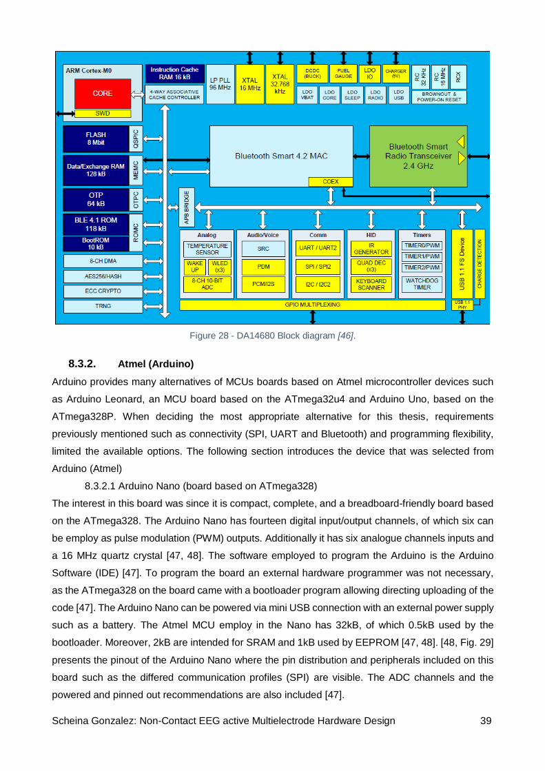
Scheina Gonzalez: Non-Contact EEG active Multielectrode Hardware Design 39
Figure 28 - DA14680 Block diagram [46].
8.3.2. Atmel (Arduino)
Arduino provides many alternatives of MCUs boards based on Atmel microcontroller devices such
as Arduino Leonard, an MCU board based on the ATmega32u4 and Arduino Uno, based on the
ATmega328P. When deciding the most appropriate alternative for this thesis, requirements
previously mentioned such as connectivity (SPI, UART and Bluetooth) and programming flexibility,
limited the available options. The following section introduces the device that was selected from
Arduino (Atmel)
8.3.2.1 Arduino Nano (board based on ATmega328)
The interest in this board was since it is compact, complete, and a breadboard-friendly board based
on the ATmega328. The Arduino Nano has fourteen digital input/output channels, of which six can
be employ as pulse modulation (PWM) outputs. Additionally it has six analogue channels inputs and
a 16 MHz quartz crystal [47, 48]. The software employed to program the Arduino is the Arduino
Software (IDE) [47]. To program the board an external hardware programmer was not necessary,
as the ATmega328 on the board came with a bootloader program allowing directing uploading of the
code [47]. The Arduino Nano can be powered via mini USB connection with an external power supply
such as a battery. The Atmel MCU employ in the Nano has 32kB, of which 0.5kB used by the
bootloader. Moreover, 2kB are intended for SRAM and 1kB used by EEPROM [47, 48]. [48, Fig. 29]
presents the pinout of the Arduino Nano where the pin distribution and peripherals included on this
board such as the differed communication profiles (SPI) are visible. The ADC channels and the
powered and pinned out recommendations are also included [47].

Scheina Gonzalez: Non-Contact EEG active Multielectrode Hardware Design 40
Figure 29 Arduino Nano Pinout [47]
8.4. MCU Comparison
It is not possible to determine which MCU should be employed for this thesis without considering the
limitations and differences of each device. Table 5 summarises the presented MCUs and their main
characteristics. Both MCUs presented here are of interest, however, the DA14680 is the most
appropriate MCU that fulfil the requirements for this project, using the ADS1298 in daisy-chain mode.
Furthermore, the BLE and has programmable charging capability, small design and a reduction of
the components required is possible. This MCU serves a platform where the project can grow on,
and it will allow a higher number of ADC. On the other hand, the Arduino Nano can be used as an
evaluation method for the electrode stage to verify its functionality due to it less complex setup and
programming.

Scheina Gonzalez: Non-Contact EEG active Multielectrode Hardware Design 41
MCU DA14680 Atmega328
Flash 8Mbit 32KB
SRAM 16KB 2KB
Clock Speed 16MHz 16MHz
Analogue I/O 31 general purpose 8
DC Current per I/O 10µA 40mA
Digital I/O - 22
Input Voltage 1.7-4.75V 7-12V (operational 5V)
Bluetooth BLE device Peripheral device
Changed mode Programmable External device
CPU type ARM Cortex –M0 AVR
SPI 2 1
I/O Supply Class 1.8, 3.3 3.3
Table 5 - MCU Comparison (Author’s own)
42 Scheina Gonzalez Non-Contact EEG active Multielectrode Hardware Design
9. Printed Circuit Boards (PCBs) Layout Design
This chapter describes the build of the different PCBs that were developed for this thesis. It also
describes how the band pass filter was designed for the electrode test without the PCB of the ADC.
To develop the circuit schematics and the PCBs, software tools were utilised, from which the required
files for the construction of the PCBS such as the Gerber files for the PCB design were obtained.
9.1. Software Tool
For the layout of the PCBs, the software Altium designer was used. This software provides a series
of tools for electronic design automation such as a broad database with components from different
brands, net listing, and 3D design and PCB visualisation. For the design and testing the amplification
stage before the PCB design the MultiSIM 14.0 from National Instruments was used. This software
allowed the testing of the readout circuit with the range of frequency for an EEG, and to simulate the
capacitive input.
9.2. EEG sensor
The final EEG sensor PCB consists of two PCBs which were soldered together; the electrode PCB
and the readout PCB. The electrode PCB, it is a two-layer PCB, where the top layer acts as the
shield, and the bottom layer as the electrode. The readout PCB is also two layers; the top layer is
the circuit tracer formed by four LMP7704, and the bottom layer is the ground plate. One problem
was the budgetary constraints for the first design, including both the electrode and readout circuit.
However, to be able to achieve this design, it was necessary to have blind vias which were used to
connect the circuit with the shield layer and electrode layer. This method increased the costs of
manufacturing the PCB, so a redesign of the PCB was necessary to obtain the final design. The
schematic of the circuit employed in the PCBS can be found in Appendix C, and D. The 3D and final
PCB layout of the developed electrode and its readout circuits can be found in Appendix E, while
Figure 30 shows a 2D drawing of the PCB design. Before sending the PCB Gerber to manufacture,
the design rule and the footprint of the components had to be carefully revised. To have a small
electrode without compromising its capacitance, the electrode and read out PCBs were restricted to
21mm diameter as seen in Figure 31. Two layer form the electrode and readout PCB, due to the
size of the PCB the tracks were reduced to the minimum manufactured size 0.102mm.
9.2.1. Consideration of the layout
As this PCB was developed for the measurement of weak and very low-level input signals such as
EEG signals, it was necessary to layout the PCB to minimise noise as much as possible. For this
reason, caution was used for some design parameters such as the shielding and the grounding.
9.2.1.1. Shielding
The purpose of using a shielding layer was to reduce the charge that it is coupled capacitively with

Scheina Gonzalez: Non-Contact EEG active Multielectrode Hardware Design 43
the readout circuit to the electrode layer. Since the shield layer has the same design as the electrode
and its proximity to the electrode layer, these two layers will be acting as a parallel-plate capacitor,
while between these layers an important dispersion capacitance will appear.
9.2.1.2. Grounding
In circuits with low frequency and low noise, it is essential to control the current pads, and in particular
the return pads. This is unlike the high-frequency circuit where return current takes the path that has
the lowest impedance, so there is a heightened risk that by employing a ground plate, the current
paths intersect and interfere with each other. Nonetheless, by using a scheme where the ground pin
possesses its own paths to the common ground layer on the PCB, the risk of the currents paths
interfering with each other can be minimised.
Figure 30 - 2D layout of the final readout PCB design Figure 31 - 3D PCB Layout (Author’s own)
9.3. Analogue Front End
The second PCB is composed of the AFE circuit, the common mode ports, and the communication
ports to the sensor PCB and the controller PCB. This is a four-layer PCB where the two middle layers
are the digital and analogue ground. The bottom contains the circuit of the ADS chip, and the
connector acts as a bridge to transfer the signal from the sensor to the ADS. The top layer includes
the battery holder, the SPI ports, and the common mode port which is the communication layer. The
schematic circuit of this PCB is presented in [Fig.32] and is configured to use a single supply
operation. The ADC employed in this design the ADS1298 as stated in the previous chapter. The
common mode was configured by employing the DRY and by obtaining the common signals from
the neighbour electrodes. A larger image of the schematic of the circuit employed in the PCBs can
be found in Appendix F. The 3D and final PCB layout can be found in Appendix G as well.

Scheina Gonzalez: Non-Contact EEG active Multielectrode Hardware Design 44
Figure 32 - ADS1298 schematic circuit (Author’s own)
9.3.1. Layout
The layout consists of a circular PCB with a 25mm of diameter with four layers. The components are
distributed between the top (connectors and battery holder) and bottom (ADC circuit) layers. Figure
33 shows a screenshot of the top layer from the PCB and design tool, while [Fig.34] shows the
bottom layer. The layers are connected by using through-hole vias. The connection to the middle
layer was conducted by through-hole vias to reduce assembly costs. Most of the components
employed in this PCB design were surface mounted excluding the common mode connector to the
neighbours.
Figure 33 - Top layer of the Analogue to digital converter PCB (Author’s own
Connection to neighbours
Battery
SPI connector

Scheina Gonzalez: Non-Contact EEG active Multielectrode Hardware Design 45
Figure 34 - Bottom layer of the analogue digital converter PCB (Author’s own)
ADC (DAS 1298)
Board to board connector

46 Scheina Gonzalez Non-Contact EEG active Multielectrode Hardware Design
9.4. BLE Layout Design
The last PCB is the BLE, containing the Bluetooth low energy MCU and an ADC, as well as the
previous PCB this board holds the common mode ports, the battery holder, and the communication
ports. This four-layer PCB has a top and bottom layer, where the bottom layer contains the ADC chip
and BLE chip, and the top layer the communication ports and the battery holder. Moreover, the
middle layer as in the previous board, it is PCB formed by an analogue and digital layer respectively.
The schematic circuit of this PCB is presented in Fig. 35. This circuit was configured to use a single
supply operation and USB charger since the BLE allows a programmable battery charger and a
capacity gauge. The BLE employed in this design the da14680 as mentioned previously. The
schematic of the circuit used in the PCBs can be found under Appendix H, while the 3D and final
PCB layout can be found under Appendix I.
Figure 35 - BLE schematic circuit (Author’s own)
9.4.1. Layout
The layout sits on a circular PCB with a 25mm of diameter with four layers. The components are
distributed between top and bottom layers, where the top layer contains the connectors and the
battery holder, while the bottom layer contains the BLE circuit, ADC circuit, and the antenna. Fig. 36
shows a screenshot from the PCB and design tool of the bottom layer, while Fig. 37 shows the top.
The layers are again connected using through hole vias. The connection to the middle layer was
conducted by through-hole vias to reduce assembly costs. Most of the components employed in this
PCB design were surface mounted excluding the common mode connector to the neighbours.

Scheina Gonzalez: Non-Contact EEG active Multielectrode Hardware Design 47
Figure 36 Bottom layer of the Bluetooth low energy MCU and Analogue to digital converter PCB (Author’s
own)
Figure 37 - Top layer of the Bluetooth low energy MCU and Analogue to digital converter PCB (Author’s
own)
ADC (DAS 1298)
BLE (da14680)
Antenna
JTAG Connector
Connection to neighbours
Battery
SPI connector
On/ off switch
Board to board connector
USB Connector

48 Scheina Gonzalez Non-Contact EEG active Multielectrode Hardware Design
10. Software developed
This section presents the code developed and the software used. Three different software were
utilised in this thesis; SmartSnippets, Matlab and Arduino integrated developer environment (IDE).
SmartSnippets was used to develop a Firmware employed to control the BLE DA14680. Matlab was
used to design the interface to display the data received from the Bluetooth, while Arduino IDE was
used to develop a code to be used to test the electrode and transmit the signal to the computer. The
language that SmartSnippets uses is C/C++, while Arduino uses Arduino language, a language
based on C/C++ (necessary?)
10.1. BLE Firmware
The development of the firmware code is important since it controls the communication with the ADC
and the transmission of the information via Bluetooth to a computer. The communication between
the ADC and the BLE device was SPI communication, this type of which requires four logical signals
such as serial clock (SCLK), Master impute Salve output (MISO), Master output slave Input (MOSI),
and Chip selection (SC) or Slave selection (SS). The communication between the BLE and computer
is done through Bluetooth. To transfer and save the developed code onto the hardware designed, a
particular circuit is employed. The DA14680 has an internal 8Mbit flash memory which was used to
save the firmware code. The hardware used to transfer the code onto the chip was the DA14681
developer kit which uses JTAG interface to debug and download the code.
10.2. BLE Code design
The firmware was based on some of the examples that are in the dialog semiconductor SDK. The
main example used was the BLE peripheral. The ADS1298.C code and header code ADS1298.H
were added to this template code to control this device via SPI. The charging stage, battery type,
and USB charging were added to the configuration due to the charging capabilities of the DA14680.
The BLE chip controls the ADS1298 via SPI protocol, and commands of the DA1298 are summarised
in [38, Tab. 6]. Read and write are two-byte commands and therefore need a second command and
data to operate, while the rest of the commands are stand-alone. First byte refers to data flows as
either write or read, and the second data bytes points out the number of registers directed after the
first register. The firmware is designed to support a maximum of 7 bytes, and the reading and writing
was done using the command WREG and the command RREG separately.
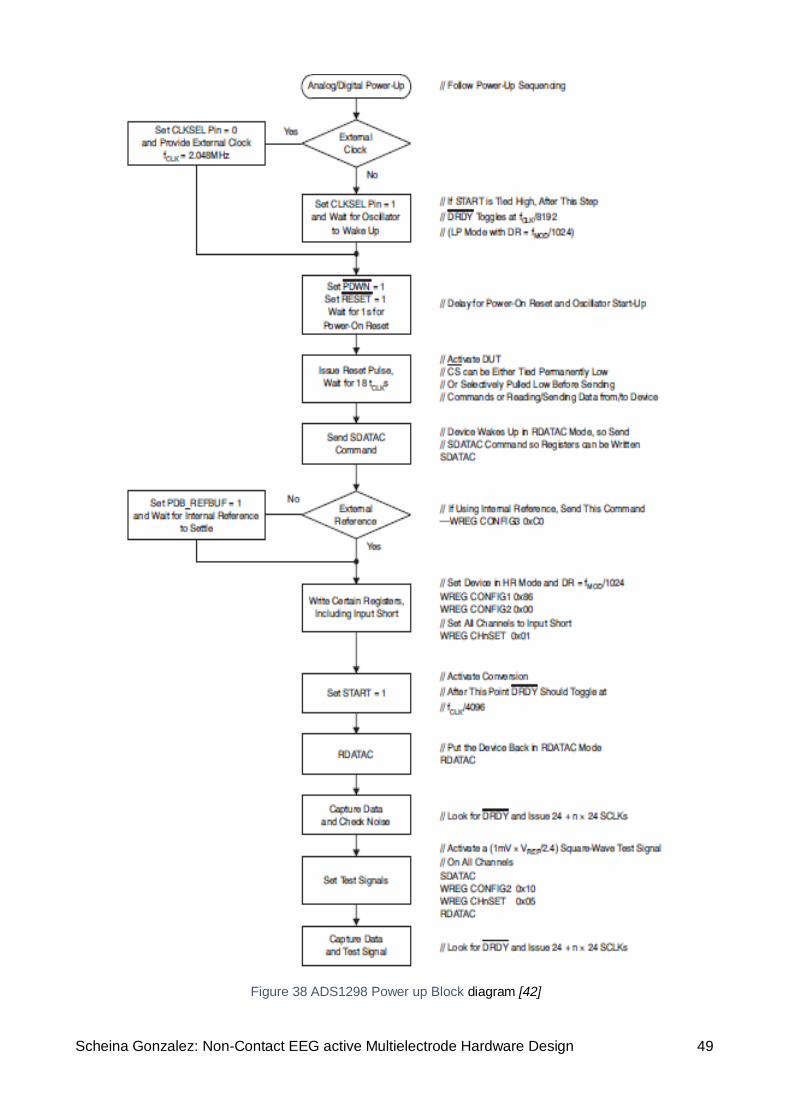
Scheina Gonzalez: Non-Contact EEG active Multielectrode Hardware Design 49
Figure 38 ADS1298 Power up Block diagram [42]

Scheina Gonzalez: Non-Contact EEG active Multielectrode Hardware Design 50
[38, Fig. 38] shows the flow diagram of the power up of the ADS1298. This sets up the register so
that when the command START is received, the communication starts at a rate of 1 KHz. For this
application, the ADC is programmed to be in reading data continuous mode, so that it is essential to
emit an SDATAC command before the command RREFG is emitted. During this stage, the MCU is
in sleep until the DRDY is inserted and an interruption occurs. After this, the BLE wakes up and the
data received is buffered and sent. This process is performed in a loop until the DRDY is asserted
and the data is sent via Bluetooth. As mentioned earlier, power consumption was key to the design,
making it necessary to sample the data at 1KHz, the maximum data rate, in order to get a better and
clear signal. The ADS1298 was programmed to work with default gain of 12; the RLD is the average
of the first four ports and port seven and eight. The positive pin of the channel 5 and six are connected
to the RLDINV; this was conducted drive the common mode from the neighbours.
Table 6 - Opcode Command Definitions [42]
10.3. Electrode Testing code
Since the ADC PCB was not built, a code in Arduino was developed. This code allows the use of the
ADC from Arduino and sending the data via Bluetooth to a computer. In addition, a code in Matlab
was developed that receives in real time the data transmitted from Arduino and plots the signal.
These two code are found in Appendix K. Since Arduino does not work with a signal smaller than
4.9 millivolt, it is necessary to deploy the amplifier and filter device. This device has a variable filter
that goes from unitary gain up to 5k v/v and has a variable low and high filter able to be made into a
band-pass filter.

51 Scheina Gonzalez Non-Contact EEG active Multielectrode Hardware Design
11. Safety
During the design and development of a medical device, it is essential to conduct a risk assessment
to ensure the safe of the device, reduce adverse events, and avoid causing any harm to the patients
or users. Furthermore, it is important to meet all the requirements of the medical devices regulatory
bodies such as Therapeutic Goods Administration (TGA) in Australia or the Food and Drug
Administration in the United States. To ensure and guarantee the safety of the design, a risk
assignment was undertaken, classifying the by employing Australian regulatory guidelines for
medical devices. The risk assessment can be found under Appendix J, while the possible risks found
are shown in Tab. 7.
Energy Hazards Chemical Hazards Information hazards
Electromagnetic energy
Induce current from external
electric field
Leakage current
Patient leakage current
Not well calibrated system
High impedance between the
body and the skin
Exposure to conductive gel
and chemicals
Mix the conductive gel
with shampoo
Warnings and maintenance
Inadequate battery management
(not removing the battery after
finishing the measurement)
Table 7 - Possible Risk and Failures (Author’s own)
To detect and prevent the potential hazards presented in Tab. 7, the following procedures were
employed:
1. After the analogue circuit design was finished, it was simulated in electronic software NI
MultiSIM to verify its functionality before assembly.
2. To reduce the electrical field induction generated by the power supply and guarantee safety
performance, this system employed a lithium coin cell battery as a battery supply.
3. This system uses a capacitive isolation between analogue and digital stage to avoid any
leakage current that may harm the subject.
4. Before human trials, a test to nullify the existence of exposed wires will be undertaken. In
addition, the system design has a wireless communication, so that will be no physical
connection to any external electrical devices.
5. This EEG design has not a chemical risk since there are no necessary chemicals or
conductive gels.
The device designed was a non-contact active segmented tripolar electrode. Since the device will
be developed and tested in Australia, it should obey Australian regulations. According to the TGA
the EEG sensor, this design falls under Rule 4.3 and Class IIa since it will be used for a direct
diagnosis or monitoring of vital physiological processes of a human subject. Moreover, the standard
that should be applied to this type of device is the IEC60601-1 medical electrical equipment standard.

52 Scheina Gonzalez Non-Contact EEG active Multielectrode Hardware Design
12. Measurement setup
This section will discuss the experiments conducted and their setup. The experiments were divided
into different stages to verifying the functionality of the electrode. The experiments were performed
in an electronics lab and some special actions were taken to try to reduce the induced noise from
the electronic devices in the lab such as turning off and disconnecting electronic devices that were
not deployed in the experiment. [Fig.39] shows a photo of the prototype capacitive active electrode
that will be tested.
Figure 39 - Segmented TCRE prototype (Author’s own)
12.1. Setup
Since the electrode designed is an active electrode, it was necessary to power it up. This was done
with a 3.6v battery instead of a DC power adapter for three reasons. Firstly to reduce or avoid
induced noise from the power line electrical field, secondly to prevent rail to rail shifting, and thirdly
to emulate the setup of the final product. Before testing the electrode on humans, it was tested by
using a sin wave signal from a signal generator. The measurement of the output signal of the
electrode was completed using a real-time digital oscilloscope. The following devices were employed
to conduct the experiments:
Keysight InfiniiVision MSO-X 2004A Mixed Signal Oscilloscope
Keysight 33500B series Waveform Generator

Scheina Gonzalez: Non-Contact EEG active Multielectrode Hardware Design 53
PM6304 Programmable automatic RCL meter
To avoid a randomness output and input and have a deterministic system, a spare PCB of the
electrode was used and connected to the wave generator, then fixed to the electrode to create a
capacitor and conduct the experiment. [Fig.40] shows the dummy electrode fixed to the prototype
electrode to create a capacitor.
Figure 40 - Sensor and dummy electrode connected back to back (Author’s own)
12.2. Capacitance Measurement
To corroborate the value of the capacitance obtained in the previous chapter, a physical
measurement of the electrode capacitance was made. To perform this measurement an RCL meter
and a metallic plate was used, as in Figure 41. Before conducting the experiment, it was necessary
to solder a wire to vias that connect the electrode layer. This wire was used as a terminal to be
attached to the RCL meter. As in [Fig. 41], the dummy electrode was placed on top of the metallic
plate and connected to the power lead of the RCL meter, and the metallic plate was connected to
the ground lead of the RCL meter. In this way, a circuit was formed with the meter and the electrode.
Table 8 presents the values obtained in the capacitance measurement. The measurement was
conducted on the dummy electrode. And the measurement was performed with and without the
solder mask on the middle and adjacent pads of the electrode to compare the result obtained

Scheina Gonzalez: Non-Contact EEG active Multielectrode Hardware Design 54
Figure 41 - Capacitance measurement (Author’s own)
Electrode section
with solder mask
Electrode section
without solder mask
Parallel 19pf 21pf
Centre electrode 12pf 12pf
Adjacent electrode 8.68pf 9.1pf
Table 7 - Capacitance measurement (Author’s own)
12.3. Filter and amplification circuit
Due to the small amplification with a gain of 21v/v of the readout circuit on the electrode and absence
of the filter, it was necessary to design a band pass filter with an extra amplification stage to perform
the electrode testing. The amplification implemented were two non-invertors with a gain of 101v/v
and 21v/v respectively. The amplifiers are connected in cascade and separated by a resistance of
100Ω. The circuit was fed using a 3.6V battery. Before tested on a human subject, it should be tested
by employing a simulation signal. In this case we employed a signal generator to emulate a signal
with amplitude and frequency like the EEG. [Tab.9] presents the Butterworth filter specifications such
as the bandwidth and the centre frequency; parameters derived from the filter transfer function.
H(s) =H0
w0Q s
s2 +w0
Q s + w02
Equation 10 - Band-pass filter transfer function [49]
Filter parameter and its calculation

Scheina Gonzalez: Non-Contact EEG active Multielectrode Hardware Design 55
Q is the selectivity of the filter as is defined as
Q =f0
BW= 0.0433
H0 is the circuit gain which is defined as the gain of the filter over the quality factor
H0 = HQ⁄ = 1276
The bandwidth (BW) of the bandpass filter is equal to the difference between the high
frequency and the low frequency
BW = fH − fL = 159.7
The centre frequency fr is the geometric mean of the high and low frequency, and it will
appear half way between fH and fl
fr = √fHfL = 6.97Hz
The high RH and low RL frequencies
RH = 51K CH = 10μf
RL = 160K CL = 10μf
fH =1
2πRHCH= 0.3Hz fL =
1
2πRLCL= 160Hz
Butterworth Filter Specifications
Bandwidth (BW) 159.7Hz
Centre Frequency (fr) 6.92Hz
Pass band ripple 0.1dB
Stop band attenuation 60dB
Circuit Gain (H0) 1276
Inner Gain 1001 v/v
Selectivity of the filter (Q) 0.0433
Low Frequency (FL) 160Hz
High Frequency (FH) 0.3Hz
Table 8 - Butterworth Filter Specifications (Author’s own)
The resulting circuit of the active filter is shown in [Fig.42]. Before it is implementation, this filter was
simulated by employing the software NI MultiSIM.

Scheina Gonzalez: Non-Contact EEG active Multielectrode Hardware Design 56
Figure 42 - Active band pass filter (Author’s own)
12.4. Electrode test
Conducting the experiment required setting up the circuit and equipment to be used, allowing the
functionality of filter and electrode to be explored. Firstly the filter stage was powered and fed with a
sinusoidal signal, allowing the circuit output to be observed. Since the electrode was designed to
have seven signal pads, 7 filters were built to see if all electrode segments were working, one for
each segment. The next step was to verify the functionality of the electrode, done by placing the
electrode and the dummy electrode back to back. The dummy electrode was fed with a signal from
the signal generator. The aim of this experiment was observing if the electrode acts as a capacitor
and receive the signal from the back of the dummy electrode. After observing the functionality of the
electrode and the filter separately, it was necessary to observe both circuits working together. For
this, each of the seven segments of the electrode was connected to each of the filters and the output
signal of each filter was observed. A Matlab filter was designed in order to get more precise values.
The code designed is presented in Appendix K. In addition, Arduino code was also designed in order
to be able to use it ADC capability and transfer the signal via Bluetooth to Matlab to be visualised
this code is also presented in Appendix K.

57 Scheina Gonzalez Non-Contact EEG active Multielectrode Hardware Design
13. Results and Discussion
This thesis was based on the design of a non-contact capacitive electrode, and the BCI design
consisting of the control and communication stage. The BCI design includes the analogue front end
which it is responsible for the digitalisation of the analogue biopotential signal, and BLE design which
is responsible for the AFE control and the communication between the BCI system and the computer.
This chapter presents the results obtained from each system level of the different designs, and the
results achieved in the implementation stage. In conformity with the structure of this paper’s
methodology, each stage was designed one at a time starting with the electrode design, AFE, then
the BLE.
13.1. Electrode design
The electrode designed in this thesis was based on the concept of a TCRE electrode due to its
capability of improving the surface Laplacian, its ability to act as a high pass filter reducing the low
frequency and increasing the spatial selectivity, and acting as a filter improving the signal-to-noise
ratio. Conventional TCREs are resistive electrodes that employ a conductive paste to improve the
connectivity between the electrode-electrolyte interfaces. Nevertheless, in this thesis a segmented
non-contact capacitive TCRE was designed, not only seeking to enjoy the advantages of the TCRE
but also to improve the spatial resolution and spatial selectivity by having more electrode in a small
area.
The result of this design was an electrode with a 20mm diameter. This electrode has three rings,
divided to obtain 8 pads which act like 8 electrodes. Each pad was designed to have the same area
with the purpose of getting the same capacitance in each electrode. The capacitance obtained
mathematically was approximately 9pf for each electrode. However, this capacitance can vary
depending on the medium. As seen in Tab.8 (section 13.2), the results are not far from the results
obtained during the experiment. In [Fig.43], a photo of the resulting electrode design is shown.
Figure 43 - Resulting electrode design (Author’s own)
During the experiment a sinusoid signal with varied amplitudes and frequency was used to observe

Scheina Gonzalez: Non-Contact EEG active Multielectrode Hardware Design 58
the behaviour of the electrode. It was found that the electrode was able to collect signals from the
dummy electrode used to emulate the electrolyte. In addition, it was observed that the signal is lost
when the amplitude is decreased. In conclusion, we stated that the problems found during the
electrode testing stage are related to the readout circuit and are specified in the following section.
13.2. Readout circuit
Since the electrode designed is a capacitive electrode, it was necessary to design a readout circuit
since the amplitude of the signal to be measured is in microvolts and the frequency of the signal is
between 1 to 100Hz. This circuit was designed to be connected directly to the electrode to form a
single device a sensor. The sensor obtained from the concession of the electrode and the readout
circuit was designed to be able to connect to the AFE level. As a result of this stage the read circuit
which is formed by a buffer stage and amplification stage with a gain of 21 v/v was obtained. This
readout circuit was designed in order to maintain the small sensor size, and since the AFE selected
can manage these small signals. In addition, the PCB which was built to be able to test the
performance of the sensor was obtained. In Fig.44 is shown the PCB of the readout circuit and the
electrode.
Figure 44 - PCB of the readout circuit and the electrode (Author’s own)
During the experimental stage, a signal generator was used to generate a signal with a higher
amplitude than the EEG signal. When the signal was tuned down to the amplitude of the EEG signal,
it was observed that the output signal decreased. It was also observed that the signal in some of the
electrodes goes up to the rail. After measuring the voltage to determine problems in each stage of
the readout circuit, it was necessary to simulate the circuit in NI MultiSIM. During this testing, results
showed that the design has a floating analogue input. This causes the signal drop and go up to the
rail. The method to resolve this problem is to redesign the circuit and add a high resistor from the
input to ground or a diode Zener from the input to ground. To validate whether the proposed solution
fixes the problem with the rail, eight mega ohms were added to the input of one of the readout
circuits. As a result of this experiment, the problem with the rail was resolved, and it was possible to
obtain a signal in the output of the sensor.

Scheina Gonzalez: Non-Contact EEG active Multielectrode Hardware Design 59
13.3. Band pass filter and Common mode circuit for the testing purpose
As stated previously, the readout circuit has an amplification gain of 21 v/v and does not have filter
stage. To be able to test the system and see the functionality of the sensor, an active band pass
filter with a gain of 100v/v and 21v/v was used. In addition, a common mode circuit to get the signal
from the mastoid and feed with the system it was designed. In [Fig.45] is shown the schematic circuit
of the Common mode and in Figure 46 is shown the circuit implementation.
Figure 45 - Common mode Circuit (Author’s own)
This section was tested separately from the sensor by using a signal generator to feed the filter and
the common mode circuit. Results show that the amplification was not as expected as the
amplification was lower, causing a drop in the signal. Despite these results, we proceeded to test
the circuits together, and as result signal was too small to be able to see. To find the problem, the
complete system was simulated by employing the software NI MultiSIM and two experiments were
conducted. First, the amplification of the commons mode was removed, however this test did not
show any improvements. For the second experiment, the common mode circuit was removed,
resulting in the system amplifying. So it was decided that the common mode stage from the testing
circuit should be eliminated, since this experiment aimed to test the capacitive measurement
functionality of the sensor. The common mode for the final design will be managed by the AFE.
13.4. Problem caused by the Power Line
From the moment the experiments started, it was observed in the oscilloscope that the system was
susceptible to noise. It was evident that the high levels of noise from the electrical field of the power
line and the noise induced from the other electrical equipment in the laboratory. During the
experiment it was observed that a 50Hz signal dominated the input, and the input signal was
attenuated and distorted as is shown in [Fig. 46a] and Fig. 46b] respectively . To minimise this
problem, the system was battery powered, and the only to electric devices near to the measurement
desk was the oscilloscope and the signal generator.

Scheina Gonzalez: Non-Contact EEG active Multielectrode Hardware Design 60
Figure 46 distorted and attenuated signals results measure in the output of the electrode
13.5. AFE and BLE circuit and PCB design
As a result of the digitalization, control and communication stage of the thesis, the selection of the
device that will perform this functions was undergone. After that, the AFE circuit design of the system
and subsequently the AFE PCB design was conducted. After completing this stage, the next result
was the BLE circuit design and its PCB. Despite having finished the designs in time, it was not
possible to build due to budgetary constraints from the cost of the PCBs. The increase in the cost of
the construction of these PCBs was due to two main issues. Firstly, the size of the BLE chip since
the minimum manufacture trace was 4 mil, and the track for the BLE design was 3 mil between the
chip pads. Secondly, the packet and the price of the AFE was high since it is preferable to send the
chips to the company that will make the PCB who can verify their performance. An additional
constraint was the time spent eliminating the bugs in the PCB design in order to ensure that the
design functioned as planned.
13.6. Causes of why the ADC and Bluetooth PCBs where not constructed
The following statement is provided in order to explain why the ADC and Bluetooth section of the
system was unable to be built within the duration of the project, primarily due to time and budgetary
constraints.
13.6.1. Budget
The budget that Flinders University grants for the development of thesis projects is usually AU$600.
However, during the project, we came to realise that this budget would short fall of what would be
necessary. One option that was available to us to help overcome this problem was leftover funds
from the budgets of previous students of my supervisor Professor Powers for the purchase of the
most expensive components of the project such as the ADC (ADS 1298) and the battery holders.
The remaining components and PCBs were to be purchased within the original $600 budget.
The price of the electrode design was high due to three primary reasons:
b. Attenuated signal from signal generator a. distorted ECG signal

Scheina Gonzalez: Non-Contact EEG active Multielectrode Hardware Design 61
1. The small (19-21mm diameter) size requirements set by Professor Powers
2. The number of chains and the number of electrodes per chain which consequently increased
the number of components
3. The use of blind vias in the PCB
To reduce the cost, it was necessary to modify the electrode PCB design, however the size
requirement remained. As a result, the cost of the remaining components and the electrode PCB
was $453.50 leaving $146.50 for the ADC and Bluetooth PCB, which was not sufficient as the cost
of the ADC and Bluetooth PCBs were high for the following reasons:
1. The size of the components, as the ADCs were 64 ball BGA and the Bluetooth was a QFN
with 60 pins, 6mm x 6mm requirement small track
2. The Bluetooth chip requires specific vias as shown in Appendix L
3. The size of the PCB requested by Professor Powers was 25mm in diameter. However, this
dimension was modified as space was not sufficient for the battery holder and the rest of the
connectors.
4. Since the components were expensive, the CSE Engineering team at the university preferred
to send the BGA components to third party to build the PCB rather than risking damage to
the components or incorrect connections being made.
5. The initial designs also used blind vias to connect the top and bottom layer of the PCB with
the digital and analogue ground layers respectively, which formed the middle layers of the
PCB. The size of these vias were smallest that the fabrication companies allowed.
6. There were three different prototype designs for the ADC and Bluetooth PCBs resulting in
the quoted price to increase in price as shown in Appendix L. To reduce the cost, a single
design was created from the three individual designs which included both components (ADC
and Bluetooth) and all connectors, however without blind vias and a larger size than the one
originally required by Professor Powers.
Nonetheless, the price reduction was not sufficient since there were additional costs required for the
installation of the ADC and Bluetooth chips. Additionally, there would have been costs incurred for
overseas shipping of the components to the company who would built it. Appendix L shows the final
quotation and email for this final PCB. This quote only includes installation of the components and
the time required by the company, while the email explains that this it does not include the price and
the time of shipping, or the price of the PCB (US$211.86 + shipping).

Scheina Gonzalez: Non-Contact EEG active Multielectrode Hardware Design 62
13.6.2. Time
Due to the complexity of the designs, the initial design of the system was finalised and sent to CSE
Engineering to check and verify the PCBs in January. Also, the shopping list of the final components
was sent. However, the verification of the PCB design and the ordering of the components was an
extensive process since before the ordering could be finalised, the design had to be revised by CSE
Engineering, approved by Professor Powers, and by the university. In relation with the verification of
the PCB; every detail of the PCB had to be checked due to the high price of the components and
the PCBs, and the cost and time to build the PCB. Since the price of the first design was high, it was
necessary to make the modifications mentioned previously (elimination of blind vias, increased size
of the tracks, and reduction of the number of PCB designs). Since the primary goal of the thesis was
the non-contact electrode, this was the first PCB to be revised by to CSE Engineering and sent for
quotation. To reduce the price of this PCB, it was necessary to modify the design into two PCBs
(electrode PCB, and readout PCB), each with two layers and without blind vias, which were then
soldered to create a four-layer non-contact electrode PCB. While the new electrode PCB was sent
for quoting, I began to work on how to modify and reduce the costs of ADC and Bluetooth PCBs.
After obtaining the final PCB design, it was sent for quotation, however it was sent back twice since
the company that was selected to build the PCB found minor errors such as the separation of some
tracks as shown in Appendix L. After correcting these errors, a final quote was obtained, along with
the approximate build time (lead time) to place the components into the PCB (3-4 weeks, excluding
shipping time and the time to construct the PCB). Taking the approximate build and shipping times
into consideration, we were left with a delivery date of 1-2 weeks after the submission date for the
thesis, assuming no issues arose causing the build to take longer.
Unfortunately, due to these time and budget constraints, the PCB was unable to be built, however
the blueprint for a non-contact EEG active multielectrode was successfully designed. Ideally, with
more time and money the design could be built and tested.
63 Scheina Gonzalez Non-Contact EEG active Multielectrode Hardware Design
14. Conclusion
EEG is the measurement of the brain’s electrical activity. This electrical activity is generated a few
centimetres below the electrode employed in the measurement of EEG. As a result of this, the
cortical current must go across different resistive levels causing a blurring effect of brain activities at
the scalp. Since every position on the scalp is a weighted sum, the volume–conduction induced
mixture is the cause of the low spatial resolution. The spatial smearing is also caused by the
necessity of using a reference electrode be able to measure the potential difference. An important
method employed to improve EEG spatial resolution is the surface Laplacian. Different methods
have been utilised to improve poor spatial resolution of EEG, while this thesis focussed on the design
of a capacitive non-contact TCRE EEG electrode. This non-contact electrode was developed with
the aim of improving the accuracy of the Laplacian estimation, increasing the communication ratio
of the EEG, and improving artefact attenuation. Moreover, this thesis aimed to design the
digitalization, control, and communication system of a BCI.
The primary goals of the project, to design a non-contact EEG active Multielectrode, was
successfully achieved as the project developed the active non-contact segmented TCRE capacitive
electrode and its readout circuit. The readout circuit was soldered to the electrode in order to obtain
an EEG sensor. During the experimental stage, it was possible to obtain a signal from the electrode.
However, because of the analogue floating input in the circuit, it was not yet possible obtain a reliable
measurement. This project has seen the successful design of the AFE and BLE circuit, and their
respective PCBs. The PCBs were then subject to the bug search stage, and are now ready to be
built. Nevertheless, it was not possible to manufacture the AFE and BLE PCBs and therefore were
not able to be tested.
The BCI system was conceived to be a battery powered to avoid the problems with the power rail,
portability, and safety of the user and subject. Since this is a biomedical device for use on humans,
it was necessary to conduct a risk assessment to eliminate possible hazards.
Future work will be carried out by student at Flinders University to build and evaluate the PCBs
designed by this thesis project. Additionally, the design of a flexible electrode is under development.

64 Scheina Gonzalez Non-Contact EEG active Multielectrode Hardware Design
15. Future Work and Recommendations
Front End. As the prototype design was completed and the PCBs ready for assembly, it would
be beneficial to the research to fabricate and build the Front-end PCB since this will improve the
evaluation and testing of the EEG designed. Due to of the limited resolution of the oscilloscope that
was employed in the electrode testing, a significant amount of noise was introduced in the output
signal, and with the front-end stage being completed would achieve a considerable reduction of the
noise, yielding an improvement on the SNRs of the output signal.
Blind and buried vias. The use of blind vias increased the cost of the PCB which was the main
reason behind eliminating their usage and the redesign of the electrode. However during assembly,
it was found that the soldering of the electrode and readout circuits had caused a short circuit in
some of the sections of the sensor. The use of buried vias will reduce the number of perforations in
the layer such as those for the electrode and shield. This will help to reduce the interference and
enhance the output signal.
Flexible electrode. Since the shape of the skull is mostly spherical and the flat sections are only
on the temporal bone; the use of flexible electrodes can mimic the shape of the skull section where
it is placed, increasing the signal collection as the entire electrode would be in direct contact with the
scalp. This would also improve the spatial resolution as all the pads of the segmented tripolar
concentric electrode would be in contact with the scalp. Work on a flexible electrode has been started
by a student who will continue with the capacitive segmented tripolar concentric EEG electrode
project.
Bluetooth transmit ion. As the Bluetooth prototype design has been completed, and the PCB is
ready for fabrication, it would be beneficial for the research to fabricate and build this PCB since this
would reduce noise since the system will be wireless and the setup and collection time would be
reduced. Even though the BLE selected presented the best characteristic for this design, the size
was too small for a prototype and increased the cost of fabrication. It would therefore be advisable
to change the BLE chip.
System Evaluation. The typical non-invasive EEG electrodes are not able to detect and
distinguishing the fingers in the sensory motors cortex. Due to the size of the electrodes. In order to
overcome this disadvantage, the design presented in this thesis constituted seven paths to increase
communication rate for the electrode and distinguish and localize signals down to a few mm.
However, the testing of this capability was not conducted since another student will conduct the
evaluation of the electrode design. The author recommends conducting a motor and sensory
experiments that confirms or rejects the hypothesis.

Scheina Gonzalez: Non-Contact EEG active Multielectrode Hardware Design 65
References
[1] Brain Vision, “Brain Vision,” 2 May 2014. [Online]. Available:
http://www.brainvision.co.uk/blog/2014/05/the-electroencephalogram-eeg/. [Accessed 2017].
[2] O. Makeyev and W. Besio, “Improving the Accuracy of Laplacian Estimation with Novel Variable
Inter-Ring Distances Concentric Ring Electrodes,” Sensors, 10 June 2016.
[3] D. Vrocher III and M. J. Lowell, “Emedicinehealth,” 4 May 2016. [Online]. Available:
http://www.emedicinehealth.com/electroencephalography_eeg/article_em.htm. [Accessed
2017].
[4] D. MCFarland, “The advantages of the surface Laplacian in brain–computer,” International
Journal of Psychophysiology, pp. 1-6, 23 July 2014.
[5] P. F. Diez, V. Mut, E. Laciar and E. Avila, “A Comparison of Monopolar and Bipolar EEG
Recordings for SSVEP Detection,” in 32nd Annual International Conference of the IEEE EMBS,
Buenos Aires, 2010.
[6] M. Spuler, “A high-speed brain-computer interface (BCI) using dry EEG electrodes,” no. 12,
2017.
[7] G. Buzsakil, C. A. Anastassiou and C. Koch, “The origin of extracellular Fields and currents -
EEG, ECoG, LFP and spikes,” Nature Reviews, vol. 17, pp. 407-420, 2012.
[8] M. Teplan, “Fundamentals of EEG Measurement,” Measurement Science Reveiw, vol. 2, no.
2, pp. 1-11, 2002.
[9] T. Kirschstein and R. Kohling, “What is the source of the EEG,” Clinical EEG and Neuroscience,
vol. 40, no. 3, pp. 146-149, July 2009.
[10] M. B. Shulman, “The clinical applications of EEG: Origins,” Epilepsy & Behavior, no. 3, pp. 393-
394, July 2002.
[11] A. Chancellor , “Electroencephalography maturing gracefully,” Practical Neurology, pp. 130-
132, 2009.
[12] N. N. Boutros, Standar EEG: A research Roadmap for Neuropsychatry, Springer, 2013.

Scheina Gonzalez: Non-Contact EEG active Multielectrode Hardware Design 66
[13] T. Ros, M. Munneke, D. Ruge, H. J. Gruzelier and C. J. Rothwell, “Endogenous control of
waking brain rhythms induces neuroplasticity in humas,” European Journal of Neuroscience,
vol. 31, no. 4, pp. 770-778, 2010.
[14] R. F. Yazicioglu, C. H. Van and R. Puers, Biopotential Readout Circuit for Portable Acquisition
Systems, Springer Science, 2009.
[15] J. G. Webster, Medical Instrumentation Aplication and Design, 4th ed., ilustrated, Ed., 2009:
Wiley.
[16] A. Searle, “Electrode performance and signal processing strategies for the discrimination of
EEG alpha waves: Implications for enviromental control by unconstrained subjects without
training,” 2000.
[17] g.tec, “g.tec medical engineering,” 1999. [Online]. Available:
http://www.gtec.at/Products/Electrodes-and-Sensors/g.Electrodes-Specs-Features.
[Accessed 2017].
[18] W. Besio , K. Koka, R. Aakula and D. Weizhong, “Tri-Polar Concentric Ring Electrode
Development for,” IEEE TRANSACTIONS ON BIOMEDICAL ENGINEERING, pp. 926-933,
2006.
[19] G. B. Prats, L. S. Gil, L. Y. Ye, J. Ibanez, C. J. Garcia and B. E. Gracia , “Flexible conceric ring
electrode for non invasive bioelectrical surface recordings,” Procedia Engineering - Elsevier ,
pp. 1223-1226, 2012.
[20] J. Guo, P. Hu and J. Tan, “Analysis of a Segmented Annular Coplanar Capacitive Tilt Sensor
with Increased Sensitivity,” Sensors, 2016.
[21] G. Peng, M. Sterling and M. Bocko, “Non-contact, Capacitive Biosensor Electrodes for
Electrostatic Charge Reduction,” IEEE, 2013.
[22] T. Wartzek, T. Lammersen, B. Eilebrecht, M. Walter and S. Leonhardt, “Triboelectricity in
Capacitive Biopotential Measurements,” IEE, vol. 58, pp. 1268-1277, 2011.
[23] T. Sullivan, S. Deiss and G. Cauwenberghs, “A Low-Noise, Non-Contact EEG/ECG Sensor,”
IEEE, pp. 154-157, 2007.
[24] Y. Chi, G. Cauwenberghs and D. Cauwenberghs, “Non-contact Low Power EEG/ECG
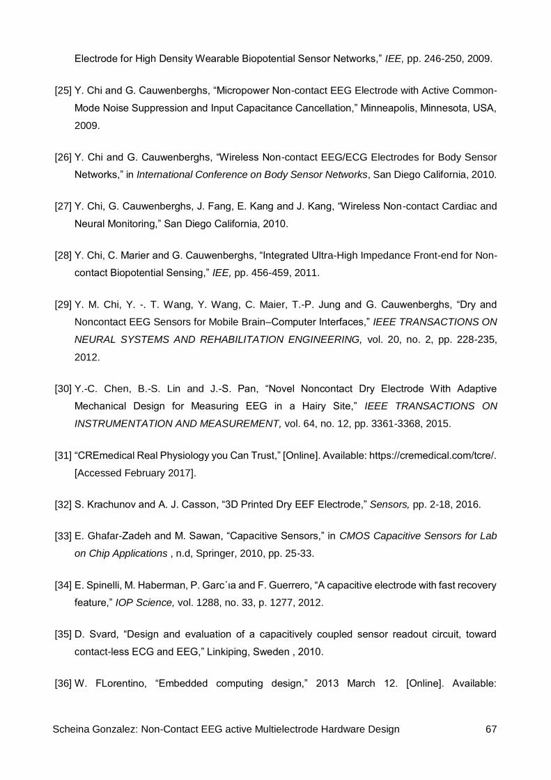
Scheina Gonzalez: Non-Contact EEG active Multielectrode Hardware Design 67
Electrode for High Density Wearable Biopotential Sensor Networks,” IEE, pp. 246-250, 2009.
[25] Y. Chi and G. Cauwenberghs, “Micropower Non-contact EEG Electrode with Active Common-
Mode Noise Suppression and Input Capacitance Cancellation,” Minneapolis, Minnesota, USA,
2009.
[26] Y. Chi and G. Cauwenberghs, “Wireless Non-contact EEG/ECG Electrodes for Body Sensor
Networks,” in International Conference on Body Sensor Networks, San Diego California, 2010.
[27] Y. Chi, G. Cauwenberghs, J. Fang, E. Kang and J. Kang, “Wireless Non-contact Cardiac and
Neural Monitoring,” San Diego California, 2010.
[28] Y. Chi, C. Marier and G. Cauwenberghs, “Integrated Ultra-High Impedance Front-end for Non-
contact Biopotential Sensing,” IEE, pp. 456-459, 2011.
[29] Y. M. Chi, Y. -. T. Wang, Y. Wang, C. Maier, T.-P. Jung and G. Cauwenberghs, “Dry and
Noncontact EEG Sensors for Mobile Brain–Computer Interfaces,” IEEE TRANSACTIONS ON
NEURAL SYSTEMS AND REHABILITATION ENGINEERING, vol. 20, no. 2, pp. 228-235,
2012.
[30] Y.-C. Chen, B.-S. Lin and J.-S. Pan, “Novel Noncontact Dry Electrode With Adaptive
Mechanical Design for Measuring EEG in a Hairy Site,” IEEE TRANSACTIONS ON
INSTRUMENTATION AND MEASUREMENT, vol. 64, no. 12, pp. 3361-3368, 2015.
[31] “CREmedical Real Physiology you Can Trust,” [Online]. Available: https://cremedical.com/tcre/.
[Accessed February 2017].
[32] S. Krachunov and A. J. Casson, “3D Printed Dry EEF Electrode,” Sensors, pp. 2-18, 2016.
[33] E. Ghafar-Zadeh and M. Sawan, “Capacitive Sensors,” in CMOS Capacitive Sensors for Lab
on Chip Applications , n.d, Springer, 2010, pp. 25-33.
[34] E. Spinelli, M. Haberman, P. Garc´ıa and F. Guerrero, “A capacitive electrode with fast recovery
feature,” IOP Science, vol. 1288, no. 33, p. 1277, 2012.
[35] D. Svard, “Design and evaluation of a capacitively coupled sensor readout circuit, toward
contact-less ECG and EEG,” Linkiping, Sweden , 2010.
[36] W. FLorentino, “Embedded computing design,” 2013 March 12. [Online]. Available:

Scheina Gonzalez: Non-Contact EEG active Multielectrode Hardware Design 68
http://embedded-computing.com/articles/latest-afe-simplifies-interfacing-hundreds-sensors/.
[Accessed 2017].
[37] E. staff, “Analog Front ENds (AFEs),” 25 February 2014. [Online]. Available:
http://www.edn.com/collections/4428913/Analog-Front-Ends--AFEs--. [Accessed 2017].
[38] Z. F. Richard, “The Evolution Of Sensor Analog Front Ends,” 24 Jun 2013. [Online]. Available:
http://www.electronicdesign.com/analog/evolution-sensor-analog-front-ends. [Accessed
2017].
[39] S. Ball, “EE Times,” 1 May 2001. [Online]. Available:
http://www.eetimes.com/document.asp?doc_id=1276974. [Accessed 2017].
[40] B. Baker, “EDN Net work,” March 16 2006. [Online]. Available: http://www.edn.com/electronics-
blogs/bakers-best/4317411/Choosing-SAR-versus-high-speed-delta-sigma-ADCs. [Accessed
2017].
[41] Texas Intrument, “ADS1299 Low-Noise, 8-Channel, 24-Bit Analog-to-Digital Converter for
Biopotential Measurements,” Texas Intrument, [Online]. Available:
http://www.ti.com/product/ADS1299. [Accessed 2017].
[42] Texas Instrumnet, “ADS1298 24-Bit, 8-Ch, Delta-Sigma ADC for ECG,” Texas Instrumnet,
[Online]. Available: http://www.ti.com/product/ADS1299. [Accessed 2017].
[43] J. D. J. Roberts, J. Ihnat and W. R. Smith, “Microprogrammed Control Unit (MCU)
PRogramming Reference Manual,” ACM Sigmicro Newsletter, vol. 3, no. 3, pp. 18-57, 1972.
[44] M. Verle, PIC Microcontrollers – Programming in Basic, MikroElektronika, Ed., 2010.
[45] B. stuff, “Bluetooth,” nd. [Online]. Available: https://www.bluetooth.com/what-is-bluetooth-
technology/how-it-works/low-energy. [Accessed 2017].
[46] Dialog Semiconductor , “SmartBond™ DA14680,” Dialog Seminconductor, 2016.
[47] Arduino Staff, “Arduino Nano,” Arduino, nd. [Online]. Available:
https://www.arduino.cc/en/Main/ArduinoBoardNano. [Accessed 2017].
[48] Atmel, “Atmel,” Nd. [Online]. Available: http://www.atmel.com/images/Atmel-8271-8-bit-AVR-
Microcontroller-ATmega48A-48PA-88A-88PA-168A-168PA-328-

Scheina Gonzalez: Non-Contact EEG active Multielectrode Hardware Design 69
328P_datasheet_Complete.pdf. [Accessed 2017].
[49] ANALOG DEVICES, “Analogue Filters,” in design-handbooks, ANALOG DEVICES, nd , p. nd
.

Scheina Gonzalez: Non-Contact EEG active Multielectrode Hardware Design 70
Appendix A: Gantt Project Planer

Scheina Gonzalez: Non-Contact EEG active Multielectrode Hardware Design 71
Appendix B: Components List
Component Distributor Quantity
LMP7704 Digikey 48
100Ω0420 0.5% Digikey 338
1KΩ 0420 0.5% Digikey 104
10K Ω 0.5% (RT0402DrD0710KL) Digikey 3
0.1Ω 1% (RUt1005FR100CS) Digikey 3
1MΩ 5% (RC0402JR-071ML) Digikey 13
20KΩ0420 0.5% Digikey 104
BKS-109-01-L-V Samtec 14
BKT-109-01-F-V Samtec 14
ADS1298 Digikey 13
DA14680 Digikey 3
503480-1400 (SPI connector) Digikey 20
68000-401HLF (RLD connector) Digikey 4
712-1005-1-ND (antenna) Digikey 4
16MHz Digikey 2
32.7680KHz Digikey 2
10033526-N3212LF (USB) Digikey 4
CVS-02TB (switch) Digikey 4
1063TR (battery holder) Digikey 14
10112684-G03-04ULF (neighbour connector) Digikey 26
M50-4900545 (Jtag connector) Digikey 4
CMD264-UBD (LED) Digikey 2
NTCG103JX103DTDS (thermistor 10KOHM) Digikey 2
MLZ1005MR47WT000 (0.47uH) Digikey 4
MLG1005S27ST000(2.7nH) Digikey 4
MLK1005S3N9ST000(3.9nH) Digikey 4
GJM1555C1H1R0BB01D (1pF) Digikey 3
JMK105BJ105KV-F(1uF) Digikey 61
GRM155R60J475ME87D(4.7uF) Digikey 12
CL05A226MQ5QUNC(22uF) Digikey 13
GRM155C80J106ME11D(10uF) Digikey 10
CL05A104MP5NNNC (0.1uF or 100nF) Digikey 61
CGA2B3X7S2A152M050BB (1.5nF or 1500pF) Digikey 4
C1005X7S2A102M050BB (1nF or 1000pF) Digikey 13
LR2032 Battery Digikey 14
Common mode electrode amazon 5
(housing connector) little bird electronic 100
M20-1160042 (crimp Socket) Digikey 100
152660139 Jtag wire connector Digikey 12
M50-9100542 (Jtag wire) Digikey 1

Scheina Gonzalez: Non-Contact EEG active Multielectrode Hardware Design 72
Appendix C: Electrode Schematic
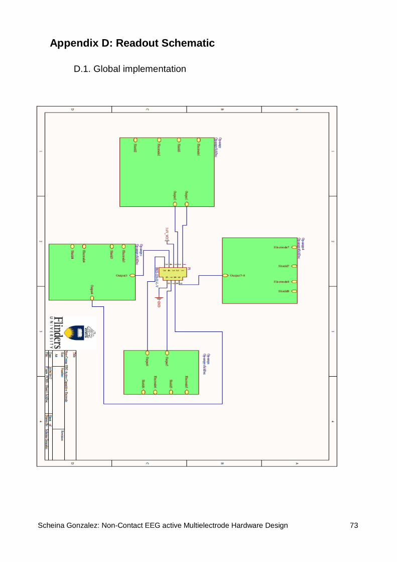
Scheina Gonzalez: Non-Contact EEG active Multielectrode Hardware Design 73
Appendix D: Readout Schematic
D.1. Global implementation

Scheina Gonzalez: Non-Contact EEG active Multielectrode Hardware Design 74
D.2. Electrode amplification circuit

Scheina Gonzalez: Non-Contact EEG active Multielectrode Hardware Design 75
D.3. Center electrode amplification circuit

Scheina Gonzalez: Non-Contact EEG active Multielectrode Hardware Design 76
Appendix E: Layout sensor
E.1. Readout PCB Layout

Scheina Gonzalez: Non-Contact EEG active Multielectrode Hardware Design 77
E.2. Electrode PCB layout

Scheina Gonzalez: Non-Contact EEG active Multielectrode Hardware Design 78
E.3. 3D Electrode PCB Print
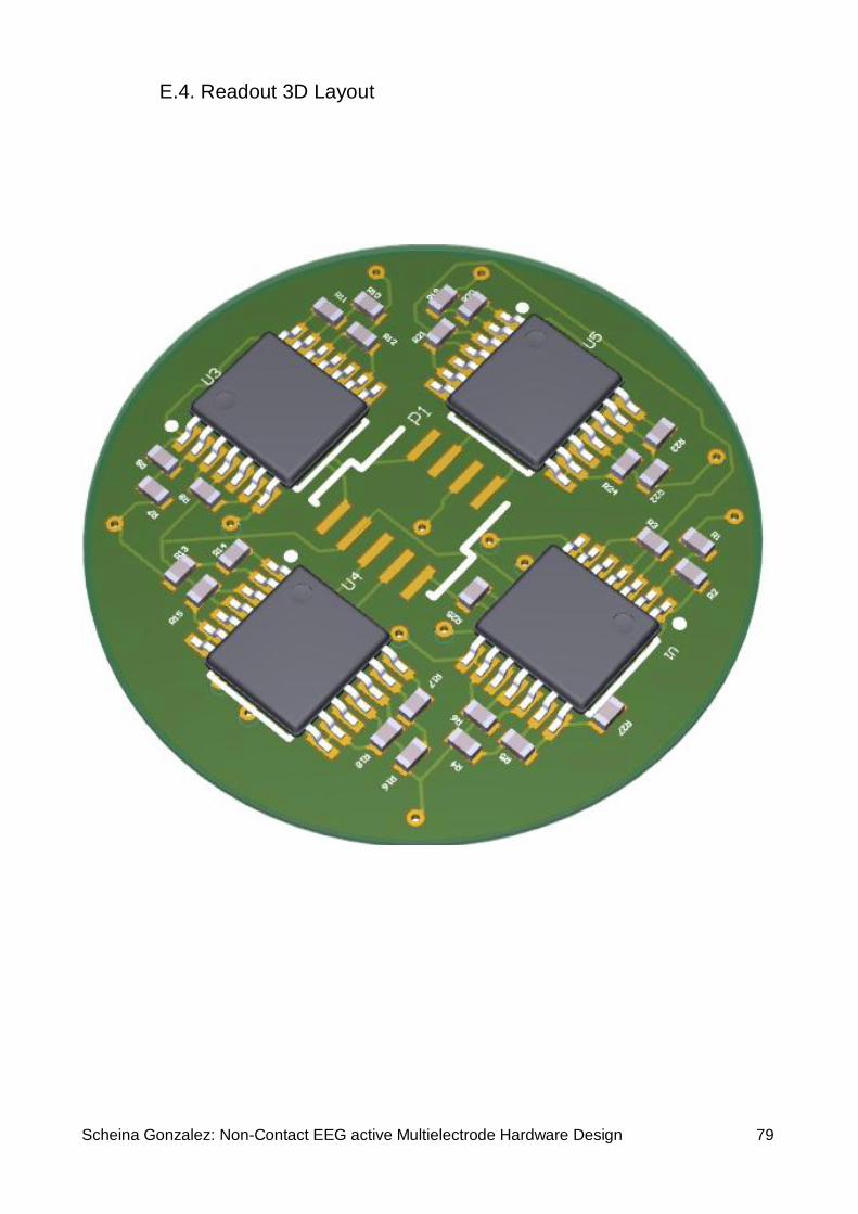
Scheina Gonzalez: Non-Contact EEG active Multielectrode Hardware Design 79
E.4. Readout 3D Layout

Scheina Gonzalez: Non-Contact EEG active Multielectrode Hardware Design 80
Appendix F: AFE Schematic
F.1. ADS1298 Schematic circuit

Scheina Gonzalez: Non-Contact EEG active Multielectrode Hardware Design 81
F.2. Digitalization Schematic Circuit

Scheina Gonzalez: Non-Contact EEG active Multielectrode Hardware Design 82
Appendix G: AFE PCB layout
G.1. 3D Top PCB Print

Scheina Gonzalez: Non-Contact EEG active Multielectrode Hardware Design 83
G.2. 3D Bottom PCB Print

Scheina Gonzalez: Non-Contact EEG active Multielectrode Hardware Design 84
G.3. Final Artwork Top Layer Print

Scheina Gonzalez: Non-Contact EEG active Multielectrode Hardware Design 85
G.4. Final Artwork Bottom Layer Print

Scheina Gonzalez: Non-Contact EEG active Multielectrode Hardware Design 86
Appendix H: BLE Schematic
H.1. DA14680 Schematic Circuit

Scheina Gonzalez: Non-Contact EEG active Multielectrode Hardware Design 87
H.2. Communication PCB Schematic circuit

Scheina Gonzalez: Non-Contact EEG active Multielectrode Hardware Design 88
Appendix I: Control and Communication PCB
I.1. 3D Top PCB Print

Scheina Gonzalez: Non-Contact EEG active Multielectrode Hardware Design 89
I.2. 3D Bottom PCB Print

Scheina Gonzalez: Non-Contact EEG active Multielectrode Hardware Design 90
I.3. Final Artwork Top Layer
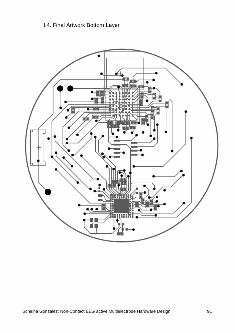
Scheina Gonzalez: Non-Contact EEG active Multielectrode Hardware Design 91
I.4. Final Artwork Bottom Layer

Scheina Gonzalez: Non-Contact EEG active Multielectrode Hardware Design 92
Appendix J: Risk assessment format

Scheina Gonzalez: Non-Contact EEG active Multielectrode Hardware Design 93
Appendix K: CODE
K.1. FRI Band pass filter
%%FIR Band Pass filter
%% is the data to be filteres
clc
clear all
Fs=10000 ; %%sample rate
t=0:(1/fs):0.05-(1/Fs);%% time vector
fn1=0.3/(Fs/2);
fn2=150/(Fs/2);
h=fir1(100,[fn1 fn2]);
freqz(h,1,50);
y=filter (h,1,x);
subplot (2,1,1)
plot(t,x);
grid
subplot (2,1,2);
plot(t,y)
grid
K.2. Bluetooth testing
K2.1. Matlab code
clear all; close all; clc;
h=waitbar(0,'Loading...'); %Wait bar is here to measure time and show when
initialization tic %is over instrhwinfo('Bluetooth'); %Command that gives back structure for communication
with Bluetooth instrhwinfo('Bluetooth','HC-06'); %Starting communication toc commandwindow close(h);
b = Bluetooth('HC-06',7); %Name of the Bluetooth module and number of data
that will be sent
fopen(b); %Opening communication port for Bluetooth
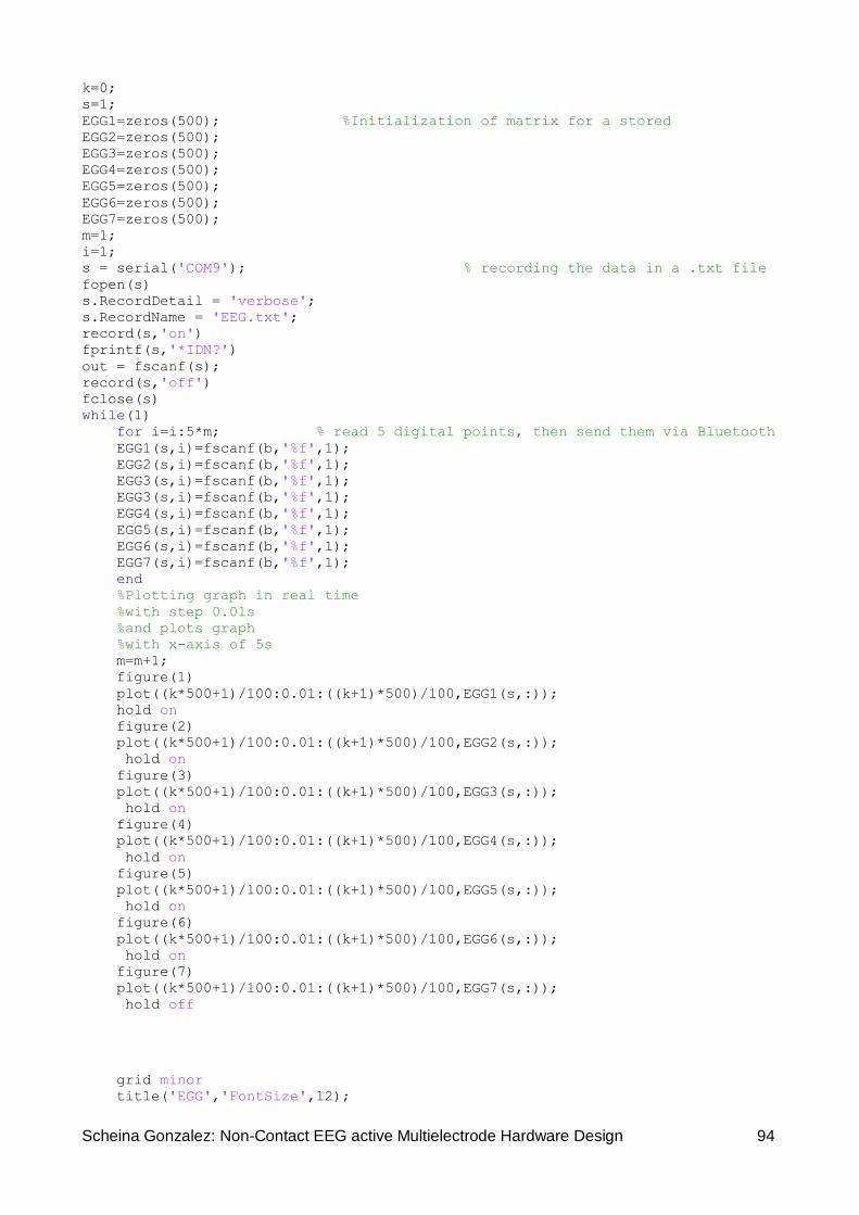
Scheina Gonzalez: Non-Contact EEG active Multielectrode Hardware Design 94
k=0; s=1; EGG1=zeros(500); %Initialization of matrix for a stored EGG2=zeros(500); EGG3=zeros(500); EGG4=zeros(500); EGG5=zeros(500); EGG6=zeros(500); EGG7=zeros(500); m=1; i=1; s = serial('COM9'); % recording the data in a .txt file fopen(s) s.RecordDetail = 'verbose'; s.RecordName = 'EEG.txt'; record(s,'on') fprintf(s,'*IDN?') out = fscanf(s); record(s,'off') fclose(s) while(1) for i=i:5*m; % read 5 digital points, then send them via Bluetooth EGG1(s,i)=fscanf(b,'%f',1); EGG2(s,i)=fscanf(b,'%f',1); EGG3(s,i)=fscanf(b,'%f',1); EGG3(s,i)=fscanf(b,'%f',1); EGG4(s,i)=fscanf(b,'%f',1); EGG5(s,i)=fscanf(b,'%f',1); EGG6(s,i)=fscanf(b,'%f',1); EGG7(s,i)=fscanf(b,'%f',1); end %Plotting graph in real time %with step 0.01s %and plots graph %with x-axis of 5s m=m+1; figure(1) plot((k*500+1)/100:0.01:((k+1)*500)/100,EGG1(s,:)); hold on figure(2) plot((k*500+1)/100:0.01:((k+1)*500)/100,EGG2(s,:)); hold on figure(3) plot((k*500+1)/100:0.01:((k+1)*500)/100,EGG3(s,:)); hold on figure(4) plot((k*500+1)/100:0.01:((k+1)*500)/100,EGG4(s,:)); hold on figure(5) plot((k*500+1)/100:0.01:((k+1)*500)/100,EGG5(s,:)); hold on figure(6) plot((k*500+1)/100:0.01:((k+1)*500)/100,EGG6(s,:)); hold on figure(7) plot((k*500+1)/100:0.01:((k+1)*500)/100,EGG7(s,:)); hold off
grid minor title('EGG','FontSize',12);

Scheina Gonzalez: Non-Contact EEG active Multielectrode Hardware Design 95
TitlePosition = 'centertop'; ylabel('amplituda[mV]','FontSize',10); xlabel('vreme[s]','FontSize',10); FontWeight = 'bold';
if (i==500) % store data in matrix, saved after plotting k=k+1; %All data will be saved in rows s=s+1; i=1; m=1;
end end
fclose(b); % close Bluetooth communication port
K2.2. Arduino code
K2.2.1. ADS1298.h
#ifndef ADS1299_H
#define ADS1299_H
#ifdef __cplusplus
namespace ADS1299 {
#endif
enum spi_command {
// system commands
WAKEUP = 0x02, // Wake up from standby mode
STANDBY = 0x04, // Enter Standby mode
RESET = 0x06, // Reset the device
START = 0x08, // Start/restart conversion
STOP = 0x0a, //Stop conversion
// read commands
RDATAC = 0x10, // ENable read data continuous mode (default mode at power up)
SDATAC = 0x11, // Stop read continuously mode
RDATA = 0x12, // read data by command; support multiple read back
// register commands
RREG = 0x20,

Scheina Gonzalez: Non-Contact EEG active Multielectrode Hardware Design 96
WREG = 0x40
};
enum reg {
// device settings
ID = 0x00,
// global settings
CONFIG1 = 0x01,
CONFIG2 = 0x02,
CONFIG3 = 0x03,
LOFF = 0x04,
// channel specific settings
CHnSET = 0x04,
CH1SET = CHnSET + 1,
CH2SET = CHnSET + 2,
CH3SET = CHnSET + 3,
CH4SET = CHnSET + 4,
CH5SET = CHnSET + 5,
CH6SET = CHnSET + 6,
CH7SET = CHnSET + 7,
CH8SET = CHnSET + 8,
RLD_SENSP = 0x0d,
RLD_SENSN = 0x0e,
LOFF_SENSP = 0x0f,
LOFF_SENSN = 0x10,
LOFF_FLIP = 0x11,
// lead off status
LOFF_STATP = 0x12,
LOFF_STATN = 0x13,
// other
GPIO = 0x14,
PACE = 0x15,
RESP = 0x16,

Scheina Gonzalez: Non-Contact EEG active Multielectrode Hardware Design 97
CONFIG4 = 0x17,
WCT1 = 0x18,
WCT2 = 0x19
};
enum ID_bits {
DEV_ID7 = 0x80,
DEV_ID6 = 0x40,
DEV_ID5 = 0x20,
DEV_ID2 = 0x04,
DEV_ID1 = 0x02,
DEV_ID0 = 0x01,
ID_const = 0x10,
ID_ADS129x = DEV_ID7,
ID_ADS129xR = (DEV_ID7 | DEV_ID6),
ID_4CHAN = 0,
ID_6CHAN = DEV_ID0,
ID_8CHAN = DEV_ID1,
ID_ADS1294 = (ID_ADS129x | ID_4CHAN),
ID_ADS1296 = (ID_ADS129x | ID_6CHAN),
ID_ADS1298 = (ID_ADS129x | ID_8CHAN),
ID_ADS1294R = (ID_ADS129xR | ID_4CHAN),
ID_ADS1296R = (ID_ADS129xR | ID_6CHAN),
ID_ADS1298R = (ID_ADS129xR | ID_8CHAN)
};
enum CONFIG1_bits {
HR = 0x80,
DAISY_EN = 0x40,
CLK_EN = 0x20,
DR2 = 0x04,
DR1 = 0x02,
DR0 = 0x01,

Scheina Gonzalez: Non-Contact EEG active Multielectrode Hardware Design 98
CONFIG1_const = 0x00,
HIGH_RES_32k_SPS = HR,
HIGH_RES_16k_SPS = (HR | DR0),
HIGH_RES_8k_SPS = (HR | DR1),
HIGH_RES_4k_SPS = (HR | DR1 | DR0),
HIGH_RES_2k_SPS = (HR | DR2),
HIGH_RES_1k_SPS = (HR | DR2 | DR0),
HIGH_RES_500_SPS = (HR | DR2 | DR1),
LOW_POWR_16k_SPS = 0x00,
LOW_POWR_8k_SPS = DR0,
LOW_POWR_4k_SPS = DR1,
LOW_POWR_2k_SPS = (DR1 | DR0),
LOW_POWR_1k_SPS = DR2,
LOW_POWR_500_SPS = (DR2 | DR0),
LOW_POWR_250_SPS = (DR2 | DR1)
};
enum CONFIG2_bits {
WCT_CHOP = 0x20,
INT_TEST = 0x10,
TEST_AMP = 0x04,
TEST_FREQ1 = 0x02,
TEST_FREQ0 = 0x01,
CONFIG2_const = 0x00,
INT_TEST_SLOW = INT_TEST,
INT_TEST_FAST = (INT_TEST | TEST_FREQ0),
INT_TEST_DC = (INT_TEST | TEST_FREQ1 | TEST_FREQ0)
};
enum CONFIG3_bits {
PD_REFBUF = 0x80,
VREF_4V = 0x20,
RLD_MEAS = 0x10,
RLDREF_INT = 0x08,
PD_RLD = 0x04,
RLD_LOFF_SENS = 0x02,

Scheina Gonzalez: Non-Contact EEG active Multielectrode Hardware Design 99
RLD_STAT = 0x01,
CONFIG3_const = 0x40
};
enum LOFF_bits {
COMP_TH2 = 0x80,
COMP_TH1 = 0x40,
COMP_TH0 = 0x20,
VLEAD_OFF_EN = 0x10,
ILEAD_OFF1 = 0x08,
ILEAD_OFF0 = 0x04,
FLEAD_OFF1 = 0x02,
FLEAD_OFF0 = 0x01,
LOFF_const = 0x00,
COMP_TH_95 = 0x00,
COMP_TH_92_5 = COMP_TH0,
COMP_TH_90 = COMP_TH1,
COMP_TH_87_5 = (COMP_TH1 | COMP_TH0),
COMP_TH_85 = COMP_TH2,
COMP_TH_80 = (COMP_TH2 | COMP_TH0),
COMP_TH_75 = (COMP_TH2 | COMP_TH1),
COMP_TH_70 = (COMP_TH2 | COMP_TH1 | COMP_TH0),
ILEAD_OFF_6nA = 0x00,
ILEAD_OFF_12nA = ILEAD_OFF0,
ILEAD_OFF_18nA = ILEAD_OFF1,
ILEAD_OFF_24nA = (ILEAD_OFF1 | ILEAD_OFF0),
FLEAD_OFF_AC = FLEAD_OFF0,
FLEAD_OFF_DC = (FLEAD_OFF1 | FLEAD_OFF0)
};
enum CHnSET_bits {
PDn = 0x80,

Scheina Gonzalez: Non-Contact EEG active Multielectrode Hardware Design 100
PD_n = 0x80,
GAINn2 = 0x40,
GAINn1 = 0x20,
GAINn0 = 0x10,
MUXn2 = 0x04,
MUXn1 = 0x02,
MUXn0 = 0x01,
CHnSET_const = 0x00,
GAIN_1X = GAINn0,
GAIN_2X = GAINn1,
GAIN_3X = (GAINn1 | GAINn0),
GAIN_4X = GAINn2,
GAIN_6X = 0x00,
GAIN_8X = (GAINn2 | GAINn0),
GAIN_12X = (GAINn2 | GAINn1),
ELECTRODE_INPUT = 0x00,
SHORTED = MUXn0,
RLD_INPUT = MUXn1,
MVDD = (MUXn1 | MUXn0),
TEMP = MUXn2,
TEST_SIGNAL = (MUXn2 | MUXn0),
RLD_DRP = (MUXn2 | MUXn1),
RLD_DRN = (MUXn2 | MUXn1 | MUXn0)
};
enum CH1SET_bits {
PD1 = 0x80,
GAIN12 = 0x40,
GAIN11 = 0x20,
GAIN10 = 0x10,
MUX12 = 0x04,
MUX11 = 0x02,
MUX10 = 0x01,

Scheina Gonzalez: Non-Contact EEG active Multielectrode Hardware Design 101
CH1SET_const = 0x00
};
enum CH2SET_bits {
PD2 = 0x80,
GAIN22 = 0x40,
GAIN21 = 0x20,
GAIN20 = 0x10,
MUX22 = 0x04,
MUX21 = 0x02,
MUX20 = 0x01,
CH2SET_const = 0x00
};
enum CH3SET_bits {
PD3 = 0x80,
GAIN32 = 0x40,
GAIN31 = 0x20,
GAIN30 = 0x10,
MUX32 = 0x04,
MUX31 = 0x02,
MUX30 = 0x01,
CH3SET_const = 0x00
};
enum CH4SET_bits {
PD4 = 0x80,
GAIN42 = 0x40,
GAIN41 = 0x20,
GAIN40 = 0x10,
MUX42 = 0x04,
MUX41 = 0x02,
MUX40 = 0x01,
CH4SET_const = 0x00

Scheina Gonzalez: Non-Contact EEG active Multielectrode Hardware Design 102
};
enum CH5SET_bits {
PD5 = 0x80,
GAIN52 = 0x40,
GAIN51 = 0x20,
GAIN50 = 0x10,
MUX52 = 0x04,
MUX51 = 0x02,
MUX50 = 0x01,
CH5SET_const = 0x00
};
enum CH6SET_bits {
PD6 = 0x80,
GAIN62 = 0x40,
GAIN61 = 0x20,
GAIN60 = 0x10,
MUX62 = 0x04,
MUX61 = 0x02,
MUX60 = 0x01,
CH6SET_const = 0x00
};
enum CH7SET_bits {
PD7 = 0x80,
GAIN72 = 0x40,
GAIN71 = 0x20,
GAIN70 = 0x10,
MUX72 = 0x04,
MUX71 = 0x02,
MUX70 = 0x01,
CH7SET_const = 0x00
};
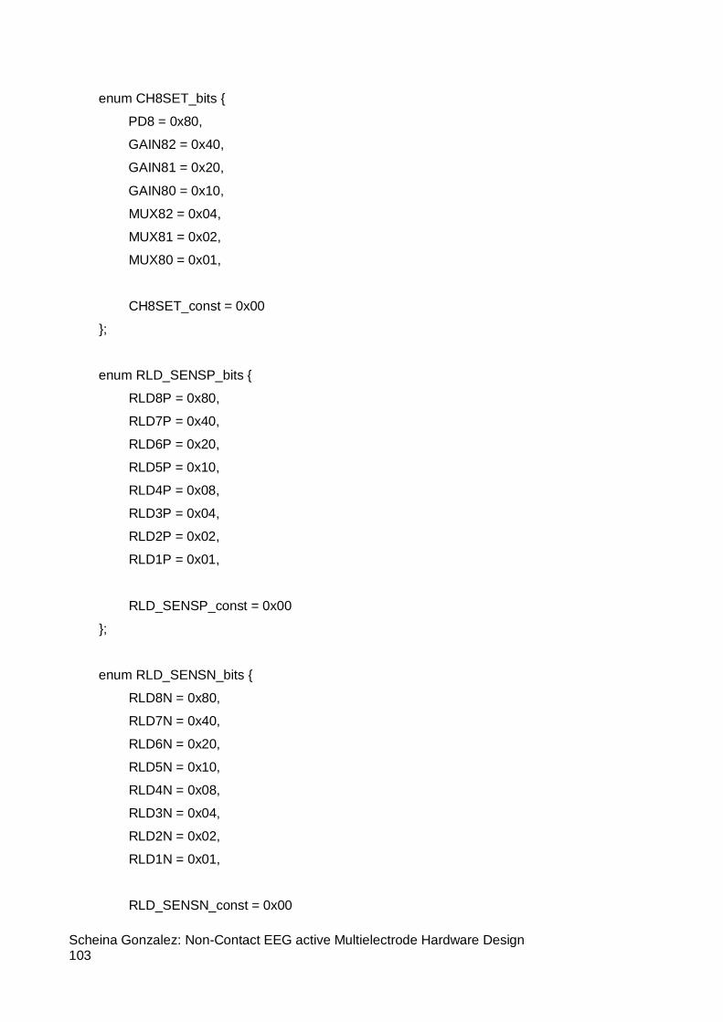
Scheina Gonzalez: Non-Contact EEG active Multielectrode Hardware Design 103
enum CH8SET_bits {
PD8 = 0x80,
GAIN82 = 0x40,
GAIN81 = 0x20,
GAIN80 = 0x10,
MUX82 = 0x04,
MUX81 = 0x02,
MUX80 = 0x01,
CH8SET_const = 0x00
};
enum RLD_SENSP_bits {
RLD8P = 0x80,
RLD7P = 0x40,
RLD6P = 0x20,
RLD5P = 0x10,
RLD4P = 0x08,
RLD3P = 0x04,
RLD2P = 0x02,
RLD1P = 0x01,
RLD_SENSP_const = 0x00
};
enum RLD_SENSN_bits {
RLD8N = 0x80,
RLD7N = 0x40,
RLD6N = 0x20,
RLD5N = 0x10,
RLD4N = 0x08,
RLD3N = 0x04,
RLD2N = 0x02,
RLD1N = 0x01,
RLD_SENSN_const = 0x00

Scheina Gonzalez: Non-Contact EEG active Multielectrode Hardware Design 104
};
enum LOFF_SENSP_bits {
LOFF8P = 0x80,
LOFF7P = 0x40,
LOFF6P = 0x20,
LOFF5P = 0x10,
LOFF4P = 0x08,
LOFF3P = 0x04,
LOFF2P = 0x02,
LOFF1P = 0x01,
LOFF_SENSP_const = 0x00
};
enum LOFF_SENSN_bits {
LOFF8N = 0x80,
LOFF7N = 0x40,
LOFF6N = 0x20,
LOFF5N = 0x10,
LOFF4N = 0x08,
LOFF3N = 0x04,
LOFF2N = 0x02,
LOFF1N = 0x01,
LOFF_SENSN_const = 0x00
};
enum LOFF_FLIP_bits {
LOFF_FLIP8 = 0x80,
LOFF_FLIP7 = 0x40,
LOFF_FLIP6 = 0x20,
LOFF_FLIP5 = 0x10,
LOFF_FLIP4 = 0x08,
LOFF_FLIP3 = 0x04,
LOFF_FLIP2 = 0x02,
LOFF_FLIP1 = 0x01,
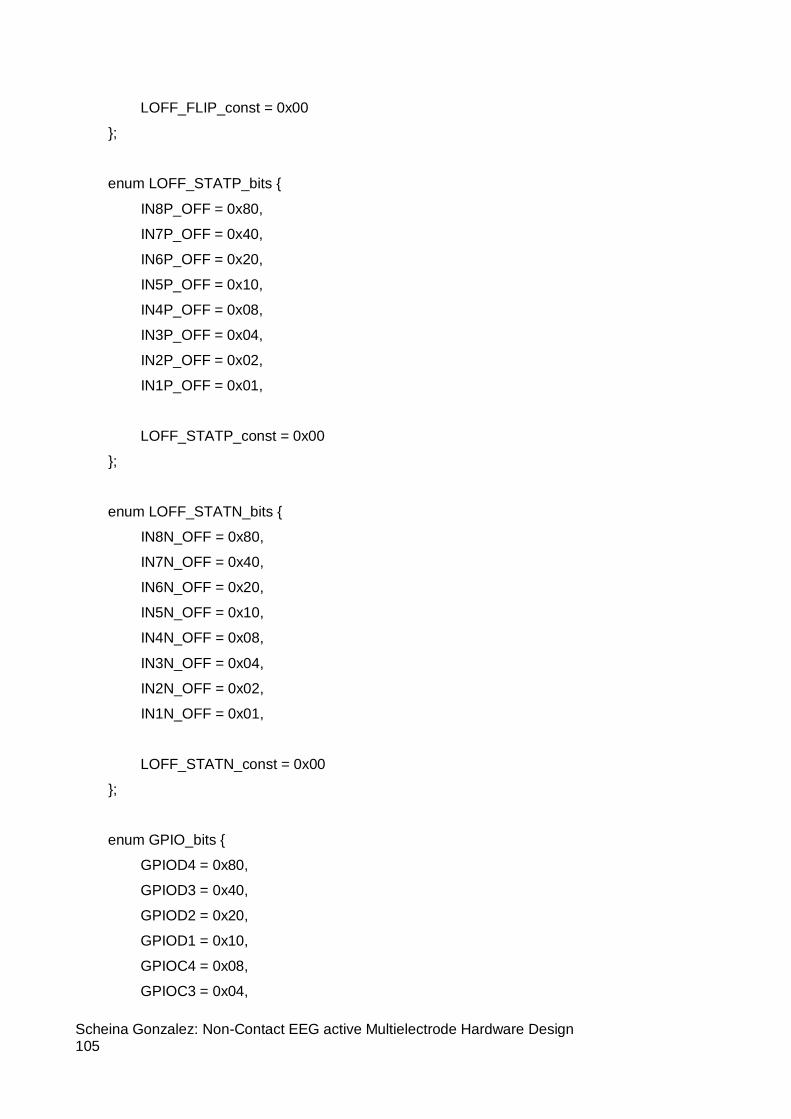
Scheina Gonzalez: Non-Contact EEG active Multielectrode Hardware Design 105
LOFF_FLIP_const = 0x00
};
enum LOFF_STATP_bits {
IN8P_OFF = 0x80,
IN7P_OFF = 0x40,
IN6P_OFF = 0x20,
IN5P_OFF = 0x10,
IN4P_OFF = 0x08,
IN3P_OFF = 0x04,
IN2P_OFF = 0x02,
IN1P_OFF = 0x01,
LOFF_STATP_const = 0x00
};
enum LOFF_STATN_bits {
IN8N_OFF = 0x80,
IN7N_OFF = 0x40,
IN6N_OFF = 0x20,
IN5N_OFF = 0x10,
IN4N_OFF = 0x08,
IN3N_OFF = 0x04,
IN2N_OFF = 0x02,
IN1N_OFF = 0x01,
LOFF_STATN_const = 0x00
};
enum GPIO_bits {
GPIOD4 = 0x80,
GPIOD3 = 0x40,
GPIOD2 = 0x20,
GPIOD1 = 0x10,
GPIOC4 = 0x08,
GPIOC3 = 0x04,

Scheina Gonzalez: Non-Contact EEG active Multielectrode Hardware Design 106
GPIOC2 = 0x02,
GPIOC1 = 0x01,
GPIO_const = 0x00
};
enum PACE_bits {
PACEE1 = 0x10,
PACEE0 = 0x08,
PACEO1 = 0x04,
PACEO0 = 0x02,
PD_PACE = 0x01,
PACE_const = 0x00,
PACEE_CHAN2 = 0x00,
PACEE_CHAN4 = PACEE0,
PACEE_CHAN6 = PACEE1,
PACEE_CHAN8 = (PACEE1 | PACEE0),
PACEO_CHAN1 = 0x00,
PACEO_CHAN3 = PACEE0,
PACEO_CHAN5 = PACEE1,
PACEO_CHAN7 = (PACEE1 | PACEE0)
};
enum CONFIG4_bits {
RESP_FREQ2 = 0x80,
RESP_FREQ1 = 0x40,
RESP_FREQ0 = 0x20,
SINGLE_SHOT = 0x08,
WCT_TO_RLD = 0x04,
PD_LOFF_COMP = 0x02,
CONFIG4_const = 0x00,
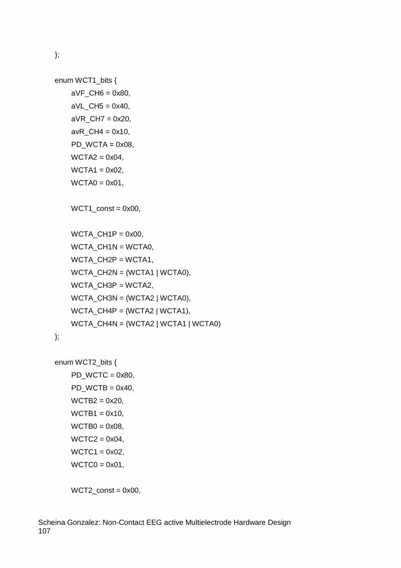
Scheina Gonzalez: Non-Contact EEG active Multielectrode Hardware Design 107
};
enum WCT1_bits {
aVF_CH6 = 0x80,
aVL_CH5 = 0x40,
aVR_CH7 = 0x20,
avR_CH4 = 0x10,
PD_WCTA = 0x08,
WCTA2 = 0x04,
WCTA1 = 0x02,
WCTA0 = 0x01,
WCT1_const = 0x00,
WCTA_CH1P = 0x00,
WCTA_CH1N = WCTA0,
WCTA_CH2P = WCTA1,
WCTA_CH2N = (WCTA1 | WCTA0),
WCTA_CH3P = WCTA2,
WCTA_CH3N = (WCTA2 | WCTA0),
WCTA_CH4P = (WCTA2 | WCTA1),
WCTA_CH4N = (WCTA2 | WCTA1 | WCTA0)
};
enum WCT2_bits {
PD_WCTC = 0x80,
PD_WCTB = 0x40,
WCTB2 = 0x20,
WCTB1 = 0x10,
WCTB0 = 0x08,
WCTC2 = 0x04,
WCTC1 = 0x02,
WCTC0 = 0x01,
WCT2_const = 0x00,

Scheina Gonzalez: Non-Contact EEG active Multielectrode Hardware Design 108
WCTB_CH1P = 0x00,
WCTB_CH1N = WCTB0,
WCTB_CH2P = WCTB1,
WCTB_CH2N = (WCTB1 | WCTB0),
WCTB_CH3P = WCTB2,
WCTB_CH3N = (WCTB2 | WCTB0),
WCTB_CH4P = (WCTB2 | WCTB1),
WCTB_CH4N = (WCTB2 | WCTB1 | WCTB0),
WCTC_CH1P = 0x00,
WCTC_CH1N = WCTC0,
WCTC_CH2P = WCTC1,
WCTC_CH2N = (WCTC1 | WCTC0),
WCTC_CH3P = WCTC2,
WCTC_CH3N = (WCTC2 | WCTC0),
WCTC_CH4P = (WCTC2 | WCTC1),
WCTC_CH4N = (WCTC2 | WCTC1 | WCTC0)
};
#ifdef __cplusplus
}
#endif /* namespace ADS1299 */
#endif
#endif /* ADS1299_H */
K2.2.2 Main code
#include <SPI.h> // include the SPI library
#include "ads1299.h"
void setup() {
// put your setup code here, to run once:
using namespace ADS1299;
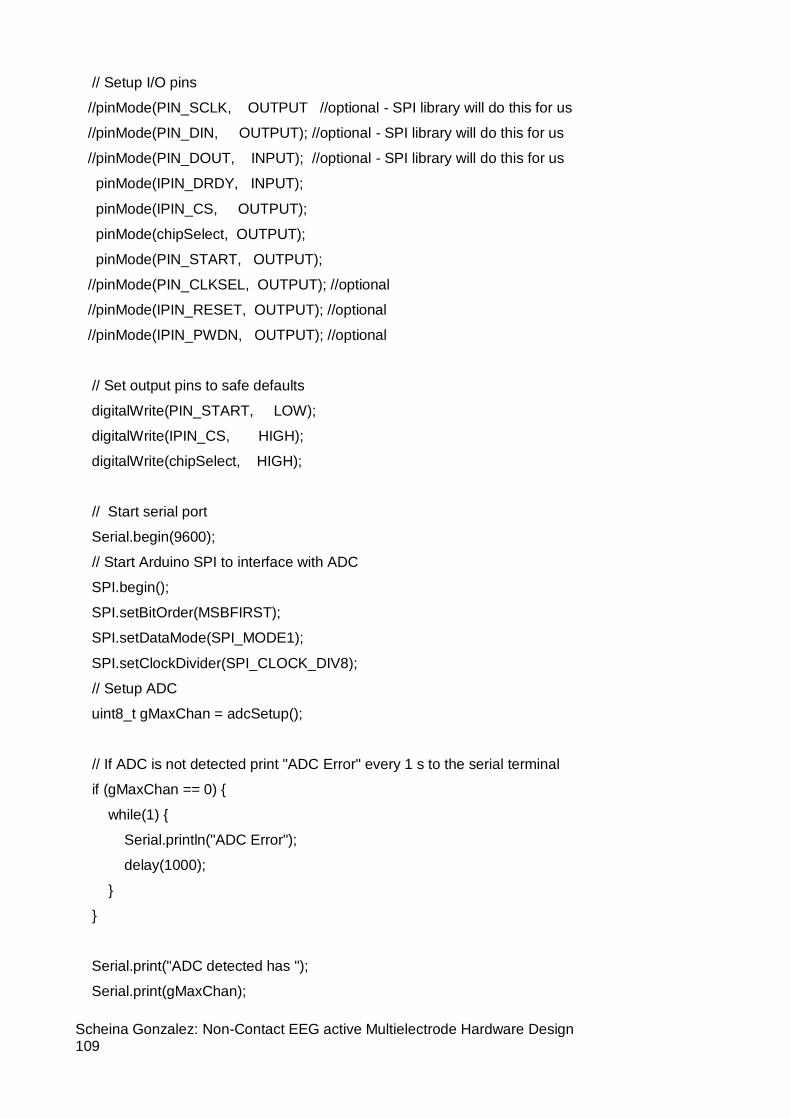
Scheina Gonzalez: Non-Contact EEG active Multielectrode Hardware Design 109
// Setup I/O pins
//pinMode(PIN_SCLK, OUTPUT //optional - SPI library will do this for us
//pinMode(PIN_DIN, OUTPUT); //optional - SPI library will do this for us
//pinMode(PIN_DOUT, INPUT); //optional - SPI library will do this for us
pinMode(IPIN_DRDY, INPUT);
pinMode(IPIN_CS, OUTPUT);
pinMode(chipSelect, OUTPUT);
pinMode(PIN_START, OUTPUT);
//pinMode(PIN_CLKSEL, OUTPUT); //optional
//pinMode(IPIN_RESET, OUTPUT); //optional
//pinMode(IPIN_PWDN, OUTPUT); //optional
// Set output pins to safe defaults
digitalWrite(PIN_START, LOW);
digitalWrite(IPIN_CS, HIGH);
digitalWrite(chipSelect, HIGH);
// Start serial port
Serial.begin(9600);
// Start Arduino SPI to interface with ADC
SPI.begin();
SPI.setBitOrder(MSBFIRST);
SPI.setDataMode(SPI_MODE1);
SPI.setClockDivider(SPI_CLOCK_DIV8);
// Setup ADC
uint8_t gMaxChan = adcSetup();
// If ADC is not detected print "ADC Error" every 1 s to the serial terminal
if (gMaxChan == 0) {
while(1) {
Serial.println("ADC Error");
delay(1000);
}
}
Serial.print("ADC detected has ");
Serial.print(gMaxChan);

Scheina Gonzalez: Non-Contact EEG active Multielectrode Hardware Design 110
Serial.print(" channels\n");
// Change SPI mode to MODE1 since that's the mode used by ADC
SPI.setDataMode(SPI_MODE1);
// Setup ADC
gMaxChan = adcSetup();
// If ADC is not detected print "ADC Error" every 1 s to the serial terminal
if (gMaxChan == 0) {
while(1) {
Serial.println("ADC Error");
delay(1000);
}
}
Serial.print("ADC detected has ");
Serial.print(gMaxChan);
Serial.print(" channels\n");
}
void loop() {
// put your main code here, to run repeatedly:
Serial.println();
}
K.2.2.3. SPI communication
// main code//
uint8_t adcSetup()
{
using namespace ADS1299;
// Power-up sequence for ADS129x
digitalWrite(IPIN_PWDN, LOW);
digitalWrite(PIN_CLKSEL, HIGH);
digitalWrite(IPIN_PWDN, HIGH);
digitalWrite(IPIN_RESET, HIGH);

Scheina Gonzalez: Non-Contact EEG active Multielectrode Hardware Design 111
delay(1000);
digitalWrite(IPIN_RESET, LOW);
delayMicroseconds(1);
digitalWrite(IPIN_RESET, HIGH);
delayMicroseconds(9);
adc_send_command(SDATAC);
delayMicroseconds(5);
// FOR RLD: Power up the internal reference
adc_wreg(CONFIG3, RLDREF_INT | PD_RLD | PD_REFBUF | CONFIG3_const);
// Only use channels IN1P and IN1N for the RLD Measurement
adc_wreg(RLD_SENSP, 0x01);
adc_wreg(RLD_SENSN, 0x01);
// All GPIO set to output 0x0000: (floating CMOS inputs can flicker on and off, creating noise)
adc_wreg(GPIO, 0x00);
// Set ADC to work at high resolution 1 KS/s sampling rate
adc_wreg(CONFIG1, HIGH_RES_1k_SPS);
// Generate internal test signal
adc_wreg(CONFIG2, INT_TEST);
// Set the all the channels as differential input with x12 gain
for (int i = 1; i <= 8; ++i) {
adc_wreg(CHnSET + i, ELECTRODE_INPUT | GAIN_12X); //report this channel with x12 gain
//adc_wreg(CHnSET + i, TEST_SIGNAL | GAIN_12X); //create square wave
//adc_wreg(CHnSET + i,SHORTED); //disable this channel
}
// Power down and short all the rest of the channels since they aren't used
//for (int i = 2; i <= 4; i++) {
// adc_wreg(CHnSET + i, PDn | SHORTED);
}
// Get ADC ID

Scheina Gonzalez: Non-Contact EEG active Multielectrode Hardware Design 112
int IDval = adc_rreg(ID) ;
switch (IDval & B00011111 ) { //5 least significant bits report channels
case B10010:
return 8; //ADS1298
break;
case B11110:
return 9; //ADS1299
break;
default:
return 0;
}
}
K.3 Smart snippets
K.3.1 ADS.c
/*
* ads.c
*
* Created on: 3 Apr 2017
* Author: schei
*/
#include "ads1298.h"
#include "hw_spi.h"
// Follow power-up sequency//
int PDWN=0;
int CLKSEL=0;
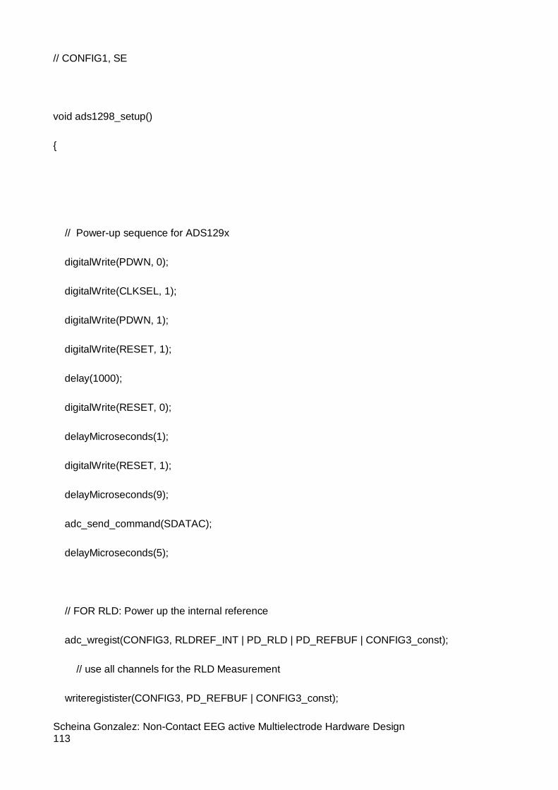
Scheina Gonzalez: Non-Contact EEG active Multielectrode Hardware Design 113
// CONFIG1, SE
void ads1298_setup()
{
// Power-up sequence for ADS129x
digitalWrite(PDWN, 0);
digitalWrite(CLKSEL, 1);
digitalWrite(PDWN, 1);
digitalWrite(RESET, 1);
delay(1000);
digitalWrite(RESET, 0);
delayMicroseconds(1);
digitalWrite(RESET, 1);
delayMicroseconds(9);
adc_send_command(SDATAC);
delayMicroseconds(5);
// FOR RLD: Power up the internal reference
adc_wregist(CONFIG3, RLDREF_INT | PD_RLD | PD_REFBUF | CONFIG3_const);
// use all channels for the RLD Measurement
writeregistister(CONFIG3, PD_REFBUF | CONFIG3_const);

Scheina Gonzalez: Non-Contact EEG active Multielectrode Hardware Design 114
// All GPIO set to output 0x0000: (floating CMOS inputs can flicker on and off, creating noise)
adc_wregist(GPIO, 0x00);
// Set ADC to work at high resolution 1 KS/s sampling rate
adc_wregist(CONFIG1, HIGH_RES_1k_SPS);
// Generate internal test signal
adc_wregist(CONFIG2, INT_TEST);
// Set the 8 channels as differential input with x8 gain
adc_wregist(CH1SET, ELECTRODE_INPUT | GAIN_8X);
adc_wregist(CH2SET, ELECTRODE_INPUT | GAIN_8X);
adc_wregist(CH3SET, ELECTRODE_INPUT | GAIN_8X);
adc_wregist(CH4SET, ELECTRODE_INPUT | GAIN_8X);
adc_wregist(CH7SET, ELECTRODE_INPUT | GAIN_8X);
adc_wregist(CH8SET, ELECTRODE_INPUT | GAIN_8X);
// adc_wregist(CH1SET, TEST_SIGNAL | GAIN_12X); //create square wave
// Power down and short all the rest of the channels since they aren't used

Scheina Gonzalez: Non-Contact EEG active Multielectrode Hardware Design 115
adc_wregist(CH6SET, PDn | SHORTED);
adc_wregist(CH5SET, PDn | SHORTED);
// Pull ADC CS pin HIGH
void ads1298 :: chipSelectHigh()
{
delayMicroseconds(3); // Wait for at least 4 tclk before pulling CS high (tclk = 2.048 MHz)
digitalWriteFast(m_chipSelectPin, HIGH);
}
void ads1298::sendcomunc(const uint8_t& comunc)
{
chipSelectLow(); // Chip select needs to be pulled low to communicate with the
device
SPI.transfer(comunc);
chipSelectHigh();
}
// Write one ADC registister
void ads1298:: writeregistister(const uint8_t& registist, const uint8_t& argum)
{
chipSelectLow();

Scheina Gonzalez: Non-Contact EEG active Multielectrode Hardware Design 116
SPI.transfer(Wregist | regist);
SPI.transfer(0x00); // Number of regististers to be read/written minus 1
SPI.transfer(argum);
chipSelectHigh();
}
// Read one ADC registister
uint8_t ads1298::readgistister(const uint8_t& registist)
{
uint8_t regist_val = 0;
chipSelectLow();
SPI.transfer(Readgist | registist);
SPI.transfer(0x00); // Number of regististers to be read/written minus 1
regist_val = SPI.transfer(0);
chipSelectHigh();
return regist_val;
}
}
}
K3.2 Main.c
/**
****************************************************************************************
*
* @file main.c
*

Scheina Gonzalez: Non-Contact EEG active Multielectrode Hardware Design 117
* @brief BLE EEG Peripheral application
*
*
* <[email protected]> and contributors.
*
****************************************************************************************
*/
/* Standard includes. */
#include <string.h>
#include <stdio.h>
#include <stdbool.h>
#include "osal.h"
#include "resmgmt.h"
#include "ad_ble.h"
#include "ad_nvms.h"
#include "ble_mgr.h"
#include "hw_gpio.h"
#include "sys_clock_mgr.h"
#include "sys_power_mgr.h"
#include "sys_watchdog.h"
#include "platform_devices.h"
#include "hw_spi.h"
#include "hw_wkup.h"
#include "hw_usb_charger.h"
#include"hw_led.h"
/* Task priorities */
#define mainTEMPLATE_TASK_PRIORITY ( OS_TASK_PRIORITY_NORMAL )
/* The configCHECK_FOR_STACK_OVERFLOW setting in FreeRTOSConifg can be used to
check task stacks for overflows. It does not however check the stack used by
interrupts. This demo has a simple addition that will also check the stack used
by interrupts if mainCHECK_INTERRUPT_STACK is set to 1. Note that this check is
only performed from the tick hook function (which runs in an interrupt context).

Scheina Gonzalez: Non-Contact EEG active Multielectrode Hardware Design 118
It is a good debugging aid - but won't catch interrupt stack problems until the
tick interrupt next executes. */
//#define mainCHECK_INTERRUPT_STACK 1
#if mainCHECK_INTERRUPT_STACK == 1
const unsigned char ucExpectedInterruptStackValues[] = { 0xCC, 0xCC, 0xCC, 0xCC, 0xCC, 0xCC,
0xCC, 0xCC, 0xCC, 0xCC, 0xCC, 0xCC, 0xCC, 0xCC, 0xCC, 0xCC };
#endif
#if dg_configUSE_WDOG
INITIALISED_PRIVILEGED_DATA int8_t idle_task_wdog_id = -1;
#endif
/*
* Perform any application specific hardware configuration. The clocks,
* memory, etc. are configured before main() is called.
*/
static void prvSetupHardware( void );
/*
* Task functions .
*/
void ble_eeg_peripheral_task(void *params);
static OS_TASK handle = NULL;
/**
* @brief System Initialization and creation of the BLE task
*/
static void system_init( void *pvParameters )
{
/* Prepare clocks. Note: cm_cpu_clk_set() and cm_sys_clk_set() can be called only from a
* task since they will suspend the task until the XTAL16M has settled and, maybe, the PLL
* is locked.
*
*/
cm_sys_clk_init(sysclk_XTAL16M);
cm_apb_set_clock_divider(apb_div1);
cm_ahb_set_clock_divider(ahb_div1);

Scheina Gonzalez: Non-Contact EEG active Multielectrode Hardware Design 119
cm_lp_clk_init();
/*
* Initialize platform watchdog
*/
sys_watchdog_init();
#if dg_configUSE_WDOG
// Register the Idle task first.
idle_task_wdog_id = sys_watchdog_register(false);
ASSERT_WARNING(idle_task_wdog_id != -1);
sys_watchdog_configure_idle_id(idle_task_wdog_id);
#endif
/* Set system clock */
cm_sys_clk_set(sysclk_XTAL16M);
/* Prepare the hardware to run this demo. */
prvSetupHardware();
/* init resources */
resource_init();
/* Set the desired sleep mode. */
pm_set_wakeup_mode(true);
pm_set_sleep_mode(pm_mode_extended_sleep);
/* Initialize BLE Manager */
ble_mgr_init();
/* Start the BLE EEG Peripheral application task. */
OS_TASK_CREATE("BLE EEG Peripheral", /* The text name assigned to the task,
for
debug only; not used by the kernel. */
ble_eeg_peripheral_task, /* The function that implements the task. */
NULL, /* The parameter passed to the task. */
200 * OS_STACK_WORD_SIZE, /* The number of bytes to allocate to the

Scheina Gonzalez: Non-Contact EEG active Multielectrode Hardware Design 120
stack of the task. */
mainBLE_EEG_PERIPHERAL_TASK_PRIORITY,/* The priority assigned to the task.
*/
handle); /* The task handle. */
OS_ASSERT(handle);
/* the work of the SysInit task is done */
OS_TASK_DELETE(OS_GET_CURRENT_TASK());
}
/*-----------------------------------------------------------*/
/**
* @brief Basic initialization and creation of the system initialization task.
*/
int main( void )
{
OS_BASE_TYPE status;
cm_clk_init_low_level(); /* Basic clock initializations. */
/* Start SysInit task. */
status = OS_TASK_CREATE("SysInit", /* The text name assigned to the task, for
debug only; not used by the kernel. */
system_init, /* The System Initialization task. */
( void * ) 0, /* The parameter passed to the task. */
1024, /* The number of bytes to allocate to the
stack of the task. */
OS_TASK_PRIORITY_HIGHEST, /* The priority assigned to the task. */
handle ); /* The task handle */
OS_ASSERT(status == OS_TASK_CREATE_SUCCESS);
/* Start the tasks and timer running. */
vTaskStartScheduler();
/* If all is well, the scheduler will now be running, and the following
line will never be reached. If the following line does execute, then
there was insufficient FreeRTOS heap memory available for the idle and/or

Scheina Gonzalez: Non-Contact EEG active Multielectrode Hardware Design 121
timer tasks to be created. See the memory management section on the
FreeRTOS web site for more details. */
for( ;; );
}
void periph_setup(void)
{
# define SPI_MISO_PORT HW_GPIO_PORT_0
# define SPI_MISO_PIN HW_GPIO_PIN_2
# define SPI_MOSI_PORT HW_GPIO_PORT_0
# define SPI_MOSI_PIN HW_GPIO_PIN_1
# define SPI_CLK_PORT HW_GPIO_PORT_0
# define SPI_CLK_PIN HW_GPIO_PIN_0
# define SPI_CS_PORT HW_GPIO_PORT_0
# define SPI_CS_PIN HW_GPIO_PIN_5
hw_gpio_configure_pin(SPI_MISO_PORT, SPI_MISO_PIN,
HW_GPIO_OUTPUT,HW_GPIO_FUNC_GPIO,1);
hw_gpio_set_pin_function(SPI_MISO_PORT, SPI_MISO_PIN, HW_GPIO_MODE_OUTPUT,
HW_GPIO_FUNC_SPI_MISO);
hw_gpio_set_pin_function(SPI_MOSI_PORT, SPI_MOSI_PIN, HW_GPIO_MODE_OUTPUT,
HW_GPIO_FUNC_SPI_MOSI);
hw_gpio_set_pin_function(SPI_CLK_PORT, SPI_CLK_PIN, HW_GPIO_MODE_OUTPUT,
HW_GPIO_FUNC_SPI_CLK);
hw_gpio_set_pin_function(SPI_CS_PORT, SPI_CS_PIN, HW_GPIO_MODE_OUTPUT,
HW_GPIO_FUNC_SPI_CS);
hw_gpio_configure_pin(CFG_SEND_16_BIT_VALUE_TRIGGER_GPIO_PORT,
CFG_SEND_16_BIT_VALUE_TRIGGER_GPIO_PIN,
HW_GPIO_MODE_INPUT_PULLUP,
HW_GPIO_FUNC_GPIO, true);
hw_gpio_configure_pin(CFG_START_ADVERTISING_TRIGGER_GPIO_PORT,

Scheina Gonzalez: Non-Contact EEG active Multielectrode Hardware Design 122
CFG_START_ADVERTISING_TRIGGER_GPIO_PIN,
HW_GPIO_MODE_INPUT_PULLUP,
HW_GPIO_FUNC_GPIO, true);
}
static void prvSetupHardware( void )
{
#if mainCHECK_INTERRUPT_STACK == 1
extern unsigned long _vStackTop[], _pvHeapStart[];
unsigned long ulInterruptStackSize;
#endif
/* Init hardware */
pm_system_init(NULL);
#if mainCHECK_INTERRUPT_STACK == 1
ulInterruptStackSize = ( ( unsigned long ) _vStackTop ) - ( ( unsigned long ) _pvHeapStart );
OS_ASSERT( ulInterruptStackSize > 350UL );
/* Fill the stack used by main() and interrupts to a known value, so its
use can be manually checked. */
memcpy( ( void * ) _pvHeapStart, ucExpectedInterruptStackValues, sizeof(
ucExpectedInterruptStackValues ) );
#endif
}
/**
* @brief Malloc fail hook
*/
void vApplicationMallocFailedHook( void )
{
taskDISABLE_INTERRUPTS();
for( ;; );
}

Scheina Gonzalez: Non-Contact EEG active Multielectrode Hardware Design 123
/**
* @brief Application idle task hook
*/
void vApplicationIdleHook( void )
{
#if dg_configUSE_WDOG
sys_watchdog_notify(idle_task_wdog_id);
#endif
}
/**
* @brief Application stack overflow hook
*/
void vApplicationStackOverflowHook( OS_TASK pxTask, char *pcTaskName )
{
( void ) pcTaskName;
( void ) pxTask;
/* Run time stack overflow checking is performed if
configCHECK_FOR_STACK_OVERFLOW is defined to 1 or 2. This hook
function is called if a stack overflow is detected. */
taskDISABLE_INTERRUPTS();
for( ;; );
}
/**
* @brief Application tick hook
*/
void vApplicationTickHook( void )
{
#if mainCHECK_INTERRUPT_STACK == 1
extern unsigned long _pvHeapStart[];

Scheina Gonzalez: Non-Contact EEG active Multielectrode Hardware Design 124
OS_ASSERT( memcmp( ( void * ) _pvHeapStart, ucExpectedInterruptStackValues, sizeof(
ucExpectedInterruptStackValues ) ) == 0U );
#endif /* mainCHECK_INTERRUPT_STACK */
}
K.3.3 system configuration
/**
\addtogroup BSP
\{
\addtogroup CONFIG
\{
\addtogroup CUSTOM
\{
*/
/**
****************************************************************************************
*
* @file custom_config_qspi.h
*****************************************************************************************
*/
#ifndef CUSTOM_CONFIG_QSPI_H_
#define CUSTOM_CONFIG_QSPI_H_
#include "bsp_definitions.h"
#define SERIAL_CONSOLE_RETARGET 1
#define CONFIG_CUSTOM_PRINT
#define CONFIG_USE_BLE
#define dg_configTESTMODE_MEASURE_SLEEP_CURRENT (0)
#define dg_configUSE_LP_CLK LP_CLK_32768
#define dg_configEXEC_MODE MODE_IS_CACHED

Scheina Gonzalez: Non-Contact EEG active Multielectrode Hardware Design 125
#define dg_configCODE_LOCATION NON_VOLATILE_IS_FLASH
#define dg_configEXT_CRYSTAL_FREQ EXT_CRYSTAL_IS_16M
#define dg_configIMAGE_SETUP DEVELOPMENT_MODE
#define dg_configEMULATE_OTP_COPY (0)
#define dg_configUSER_CAN_USE_TIMER1 (0)
/*
* Controls the retRAM size used by the project.
* 0: all RAM is retained
* 1: retention memory size is optimal
*/
#define proj_configOPTIMAL_RETRAM (0)
#if !defined(RELEASE_BUILD) && (proj_configOPTIMAL_RETRAM == 1)
/* WARNING: retRAM optimizations are disabled in DEBUG builds! */
#undef proj_configOPTIMAL_RETRAM
#define proj_configOPTIMAL_RETRAM (0)
#elif (dg_configEXEC_MODE != MODE_IS_CACHED)
/* WARNING: retRAM optimizations are not applicable in MIRRORED mode! */
#undef proj_configOPTIMAL_RETRAM
#define proj_configOPTIMAL_RETRAM (0)
#endif
#if (proj_configOPTIMAL_RETRAM == 0)
#define dg_configMEM_RETENTION_MODE (0x1F)
#define dg_configSHUFFLING_MODE (0x3)
#else
#define dg_configMEM_RETENTION_MODE (0x14)
#define dg_configSHUFFLING_MODE (0x2)
#endif
#define dg_configUSE_WDOG (0)
#define dg_configFLASH_CONNECTED_TO (FLASH_CONNECTED_TO_1V8)

Scheina Gonzalez: Non-Contact EEG active Multielectrode Hardware Design 126
#define dg_configFLASH_POWER_DOWN (0)
#define dg_configPOWER_1V8_ACTIVE (1)
#define dg_configPOWER_1V8_SLEEP (1)
#define dg_configBATTERY_TYPE (BATTERY_TYPE_LIMN2O4)
#define dg_configBATTERY_CHARGE_CURRENT 2 // 30mA
#define dg_configBATTERY_PRECHARGE_CURRENT 20 // 2.1mA
#define dg_configBATTERY_CHARGE_NTC 0 // disabled
#define dg_configUSE_USB 0
#define dg_configUSE_USB_CHARGER 1
#define dg_configUSE_USB_ENUMERATION 0
#define dg_configALLOW_CHARGING_NOT_ENUM 1
#define dg_configUSE_NOT_ENUM_CHARGING_TIMEOUT 0
#define dg_configUSE_ProDK (1)
#define dg_configUSE_SW_CURSOR (1)
#define dg_configCACHEABLE_QSPI_AREA_LEN (NVMS_PARAM_PART_start -
MEMORY_QSPIF_BASE)
/*************************************************************************************************\
* FreeRTOS specific config
*/
#define OS_FREERTOS /* Define this to use FreeRTOS */
#define configTOTAL_HEAP_SIZE 16384 /* This is the FreeRTOS Total Heap Size */
/*************************************************************************************************\
* Peripheral specific config
*/
#define dg_configFLASH_ADAPTER 1
#define dg_configNVMS_ADAPTER 1
#define dg_configNVMS_VES 1
#define dg_configGPADC_ADAPTER 1
#define dg_configUSE_HW_SPI (1)
#define dg_configUSE_HW_RF (1)

Scheina Gonzalez: Non-Contact EEG active Multielectrode Hardware Design 127
#define dg_configUSE_HW_TIMER0 (1)
#define dg_configUSE_HW_TIMER2 (1)
#define dg_configSPI_ADAPTER (1)
#define dg_configUART_ADAPTER (1)
#define dg_configRF_ADAPTER (0)
/*************************************************************************************************\
* BLE device config
*/
#define dg_configBLE_CENTRAL (0)
#define dg_configBLE_GATT_CLIENT (0)
#define dg_configBLE_OBSERVER (0)
#define dg_configBLE_BROADCASTER (0)
#define dg_configBLE_L2CAP_COC (0)
/* Include bsp default values */
#include "bsp_defaults.h"
/*************************************************************************************************\
* Memory layout configuration
*/
#if (dg_configCODE_LOCATION == NON_VOLATILE_IS_OTP)
// CODE_SIZE cannot be more than 58K
#define CODE_SIZE ( 58 * 1024)
#if (dg_configEXEC_MODE == MODE_IS_CACHED)
/* DA14681-01
* RAM goes first, RetRAM0 follows. RetRAM1 is added at the beginning when
* optimized RetRAM configuration is used (so that the IVT is preserved).
* RAM size should be defined such that it covers the whole empty space
* between RetRAM1, if it exists, and RetRAM0.
*/
#define RETRAM_FIRST 0
#define RAM_SIZE ( 64 * 1024)

Scheina Gonzalez: Non-Contact EEG active Multielectrode Hardware Design 128
#if (proj_configOPTIMAL_RETRAM == 0)
#define RETRAM_0_SIZE ( 64 * 1024)
#define RETRAM_1_SIZE ( 0 * 1024)
#else
#define RETRAM_0_SIZE ( 32 * 1024)
#define RETRAM_1_SIZE ( 32 * 1024)
#endif
#else // MIRRORED
/* DA14681-01
* CODE is first, RetRAM follows. RAM is last, always 16K.
*
* RetRAM uses all RAM5 block. RAM uses CACHE.
*/
#define RETRAM_FIRST 1
#define RAM_SIZE ( 16 * 1024)
#define RETRAM_0_SIZE (128 * 1024 - CODE_SIZE)
#define RETRAM_1_SIZE ( 0 * 1024)
#endif
#if (CODE_SIZE > (58 * 1024))
#error "maximum CODE size when OTP is used is 58K!"
#endif
#elif (dg_configCODE_LOCATION == NON_VOLATILE_IS_FLASH)
#define CODE_SIZE (128 * 1024)
#if (dg_configEXEC_MODE == MODE_IS_CACHED)
/* DA14681-01
* RAM goes first, RetRAM0 follows. RetRAM1 is added at the beginning when
* optimized RetRAM configuration is used (so that the IVT is preserved).
*/
#define RETRAM_FIRST 0
#define RAM_SIZE ( 64 * 1024)
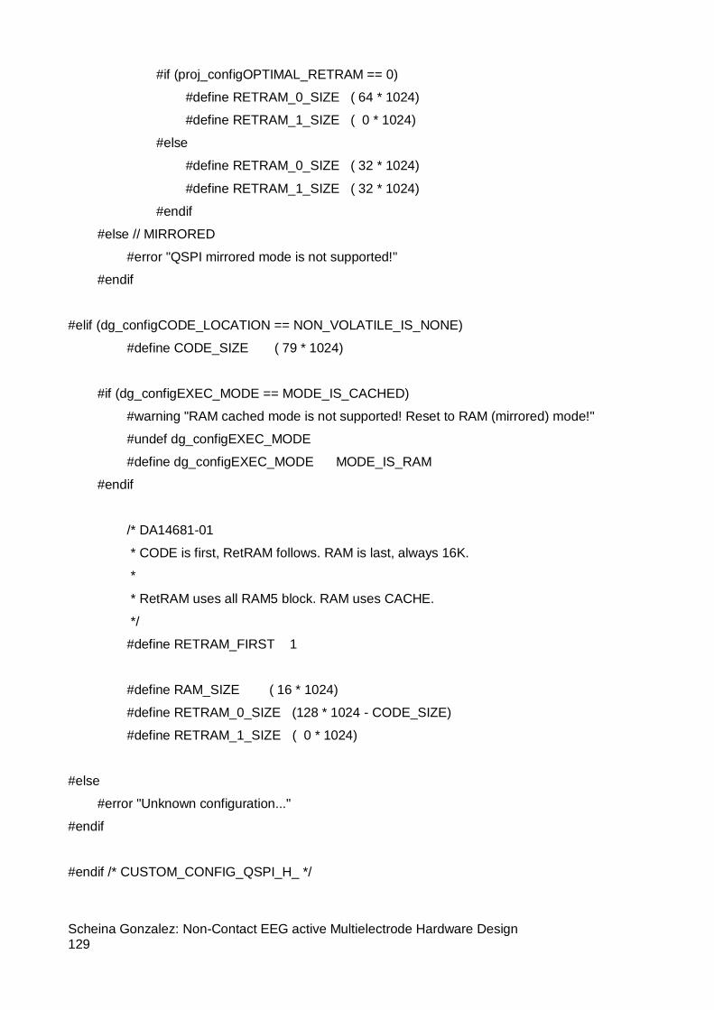
Scheina Gonzalez: Non-Contact EEG active Multielectrode Hardware Design 129
#if (proj_configOPTIMAL_RETRAM == 0)
#define RETRAM_0_SIZE ( 64 * 1024)
#define RETRAM_1_SIZE ( 0 * 1024)
#else
#define RETRAM_0_SIZE ( 32 * 1024)
#define RETRAM_1_SIZE ( 32 * 1024)
#endif
#else // MIRRORED
#error "QSPI mirrored mode is not supported!"
#endif
#elif (dg_configCODE_LOCATION == NON_VOLATILE_IS_NONE)
#define CODE_SIZE ( 79 * 1024)
#if (dg_configEXEC_MODE == MODE_IS_CACHED)
#warning "RAM cached mode is not supported! Reset to RAM (mirrored) mode!"
#undef dg_configEXEC_MODE
#define dg_configEXEC_MODE MODE_IS_RAM
#endif
/* DA14681-01
* CODE is first, RetRAM follows. RAM is last, always 16K.
*
* RetRAM uses all RAM5 block. RAM uses CACHE.
*/
#define RETRAM_FIRST 1
#define RAM_SIZE ( 16 * 1024)
#define RETRAM_0_SIZE (128 * 1024 - CODE_SIZE)
#define RETRAM_1_SIZE ( 0 * 1024)
#else
#error "Unknown configuration..."
#endif
#endif /* CUSTOM_CONFIG_QSPI_H_ */

Scheina Gonzalez: Non-Contact EEG active Multielectrode Hardware Design 130
/**
\}
\}
\}
*/

Scheina Gonzalez: Non-Contact EEG active Multielectrode Hardware Design 131
Appendix L
L.1. Vias specifications of the Bluetooth chip

Scheina Gonzalez: Non-Contact EEG active Multielectrode Hardware Design 132

Scheina Gonzalez: Non-Contact EEG active Multielectrode Hardware Design 133
L.2. first quoting of the designs

Scheina Gonzalez: Non-Contact EEG active Multielectrode Hardware Design 134

Scheina Gonzalez: Non-Contact EEG active Multielectrode Hardware Design 135

Scheina Gonzalez: Non-Contact EEG active Multielectrode Hardware Design 136

Scheina Gonzalez: Non-Contact EEG active Multielectrode Hardware Design 137

Scheina Gonzalez: Non-Contact EEG active Multielectrode Hardware Design 138
L.3. final quotation of the ADC and Bluetooth design
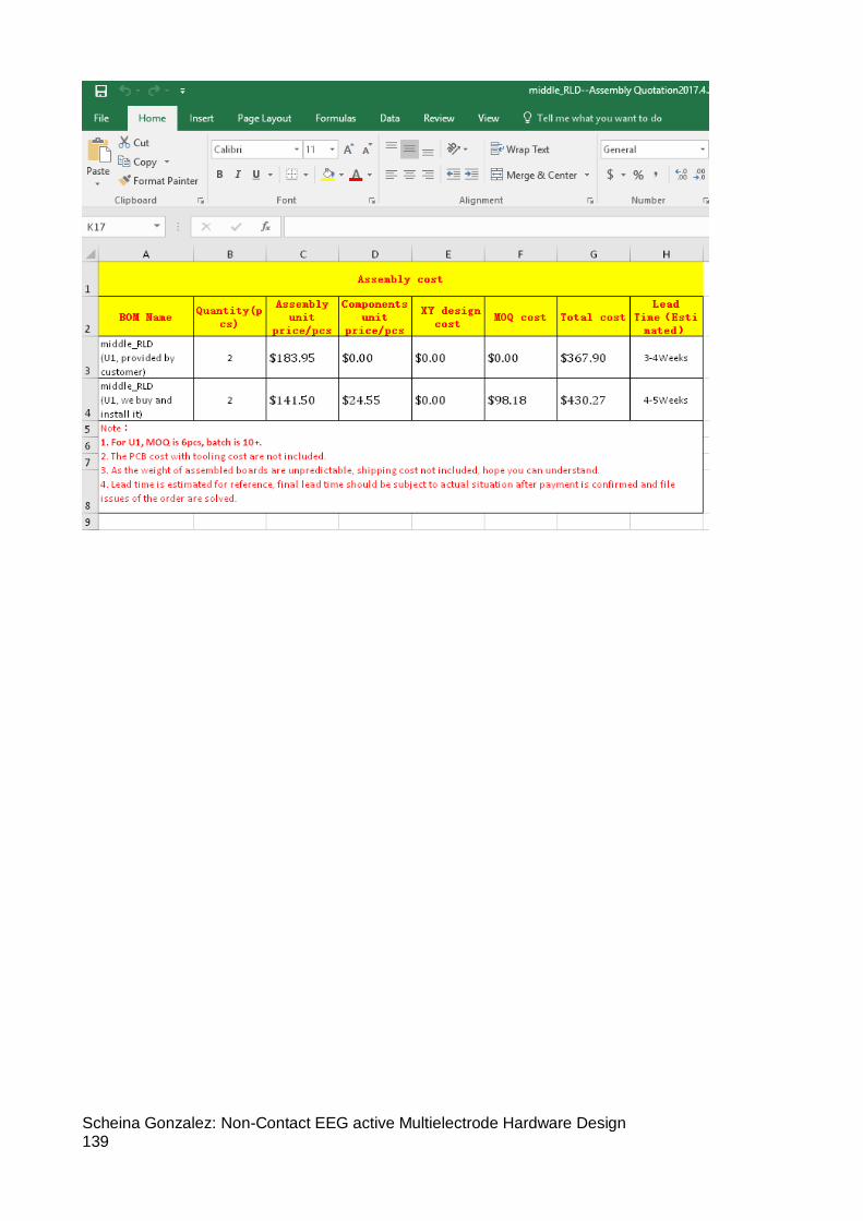
Scheina Gonzalez: Non-Contact EEG active Multielectrode Hardware Design 139
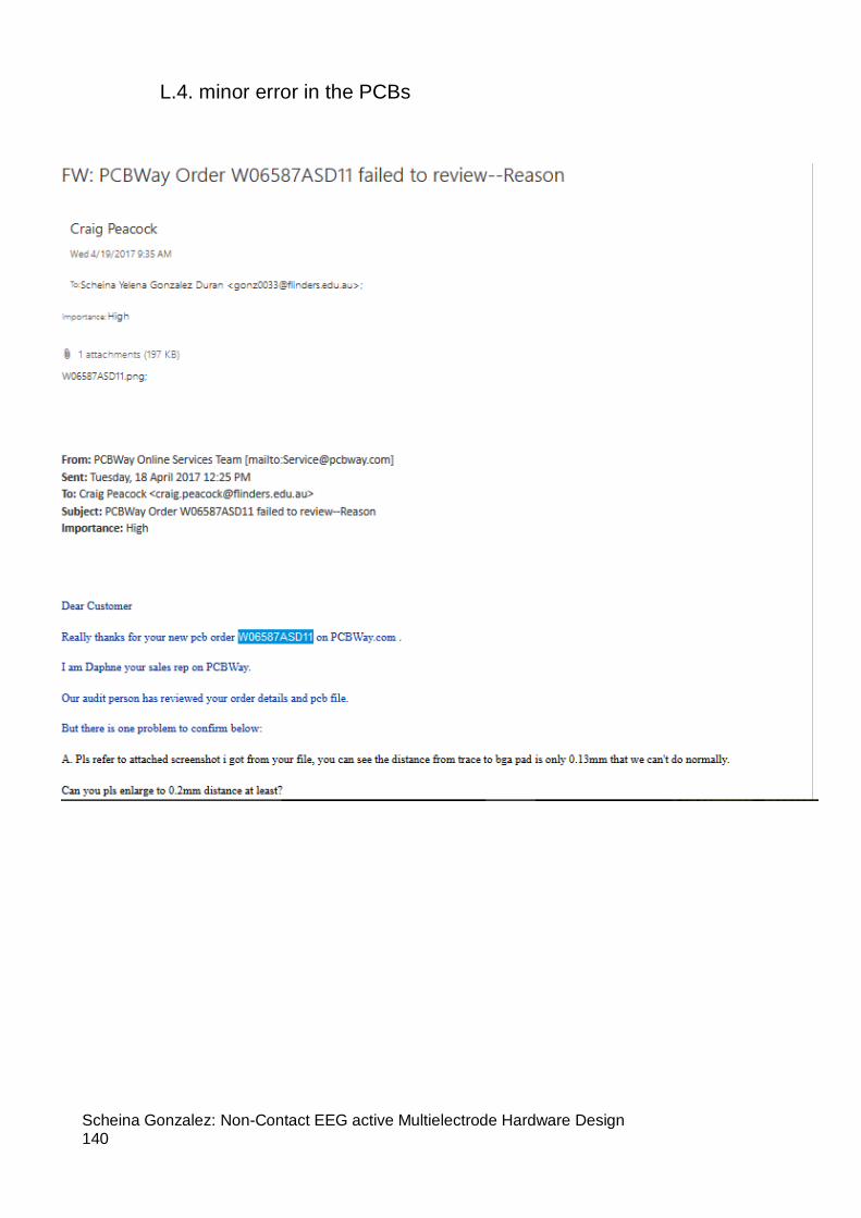
Scheina Gonzalez: Non-Contact EEG active Multielectrode Hardware Design 140
L.4. minor error in the PCBs

Scheina Gonzalez: Non-Contact EEG active Multielectrode Hardware Design 141


![NSF Project EEG CIRCUIT DESIGN. Micro-Power EEG Acquisition SoC[10] Electrode circuit EEG sensing Interference.](https://static.fdocuments.net/doc/165x107/56649cfb5503460f949ccecd/nsf-project-eeg-circuit-design-micro-power-eeg-acquisition-soc10-electrode.jpg)