PSB H- chicane magnets: Inconel vacuum chamber option & consequences on beam dynamics
description
New PSB Beam ControlClock issues
Working group meeting 01/02/2010 1/12A. Blas, P. Leinonen, J. Sanchez-Quesada
Participants:Pablo Alvarez-Sanchez, Maria Elena Angoletta, Alfred Blas, Petri Leinonen,John Molendijk, Jorge Sanchez-Quesada, Maarten Schokker, Javier Serrano,Erik Van Der Bij
New PSB Beam ControlClock issues
Working group meeting 01/02/2010 2/12
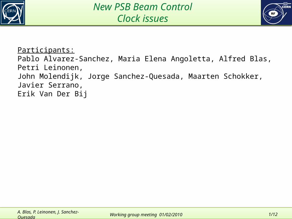
Clock source
A. Blas, P. Leinonen, J. Sanchez-Quesada
New PSB Beam ControlClock issues
3/12
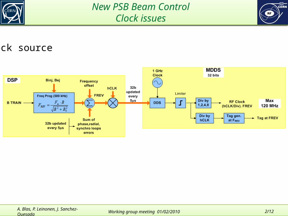
Clock in its context (typical simple loop)
A. Blas, P. Leinonen, J. Sanchez-Quesada Working group meeting 01/02/2010
New PSB Beam ControlClock issues
4/12
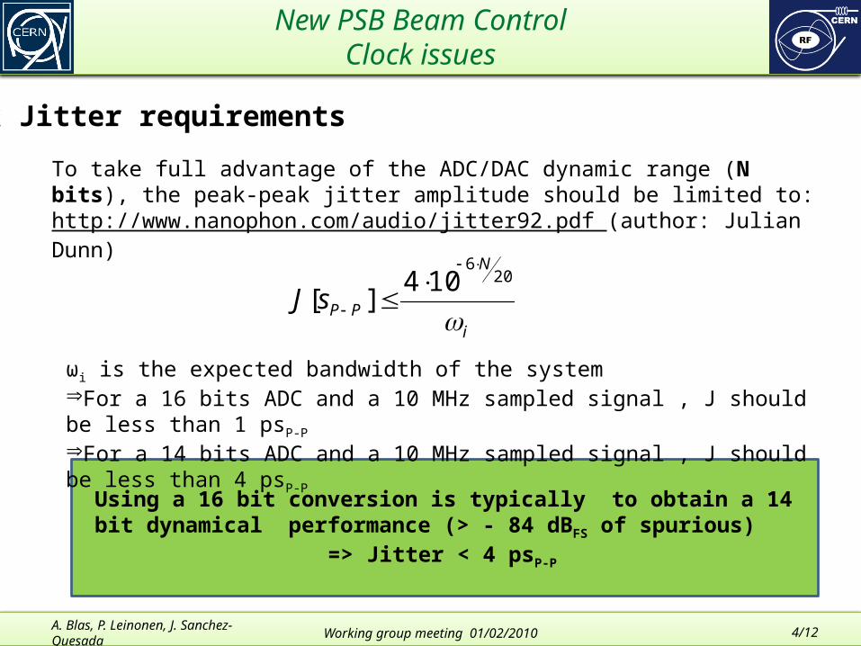
Clock Jitter requirements
i
N
PPsJ
206
104][
ωi is the expected bandwidth of the systemÞFor a 16 bits ADC and a 10 MHz sampled signal , J should be less than 1 psP-P ÞFor a 14 bits ADC and a 10 MHz sampled signal , J should be less than 4 psP-P
To take full advantage of the ADC/DAC dynamic range (N bits), the peak-peak jitter amplitude should be limited to:http://www.nanophon.com/audio/jitter92.pdf (author: Julian Dunn)
Using a 16 bit conversion is typically to obtain a 14 bit dynamical performance (> - 84 dBFS of spurious)
=> Jitter < 4 psP-P
A. Blas, P. Leinonen, J. Sanchez-Quesada Working group meeting 01/02/2010
New PSB Beam ControlClock issues
5/12
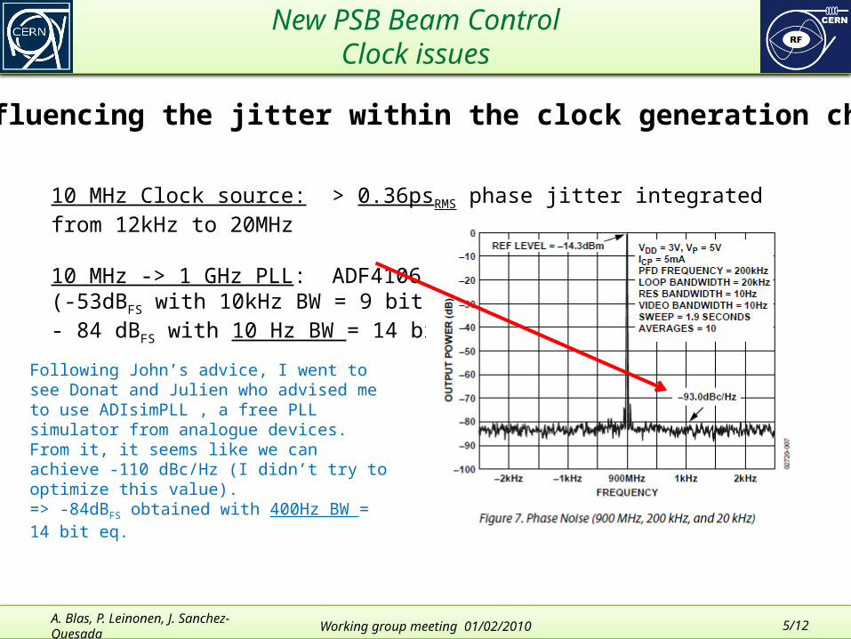
Elements influencing the jitter within the clock generation chain
10 MHz Clock source: > 0.36psRMS phase jitter integrated from 12kHz to 20MHz
10 MHz -> 1 GHz PLL: ADF4106(-53dBFS with 10kHz BW = 9 bit eq.- 84 dBFS with 10 Hz BW = 14 bit eq.)
A. Blas, P. Leinonen, J. Sanchez-Quesada Working group meeting 01/02/2010
Following John’s advice, I went to see Donat and Julien who advised me to use ADIsimPLL , a free PLL simulator from analogue devices. From it, it seems like we can achieve -110 dBc/Hz (I didn’t try to optimize this value).=> -84dBFS obtained with 400Hz BW = 14 bit eq.
New PSB Beam ControlClock issues
6/12
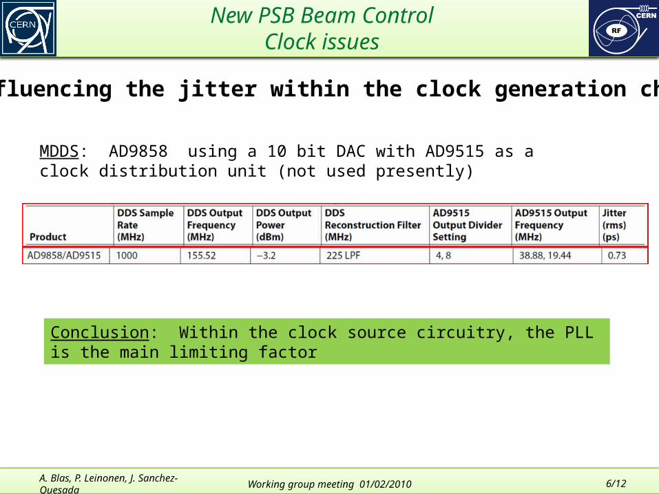
Elements influencing the jitter within the clock generation chain
MDDS: AD9858 using a 10 bit DAC with AD9515 as a clock distribution unit (not used presently)
Conclusion: Within the clock source circuitry, the PLL is the main limiting factor
A. Blas, P. Leinonen, J. Sanchez-Quesada Working group meeting 01/02/2010
New PSB Beam ControlClock issues
7/12
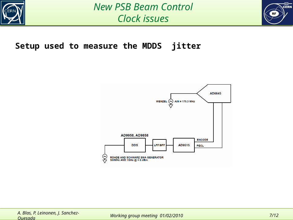
Setup used to measure the MDDS jitter
A. Blas, P. Leinonen, J. Sanchez-Quesada Working group meeting 01/02/2010
New PSB Beam ControlClock issues
8/12
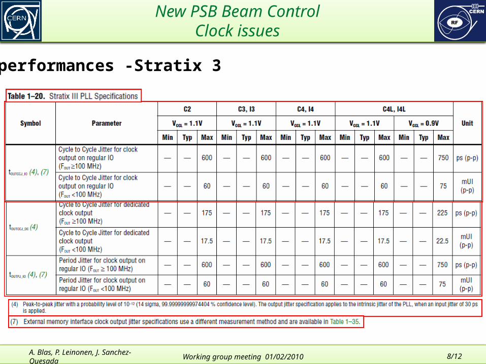
FPGA performances -Stratix 3
A. Blas, P. Leinonen, J. Sanchez-Quesada Working group meeting 01/02/2010

New PSB Beam ControlClock issues
9/12
FPGA performances -Stratix 3
A. Blas, P. Leinonen, J. Sanchez-Quesada Working group meeting 01/02/2010
New PSB Beam ControlClock issues
10/12
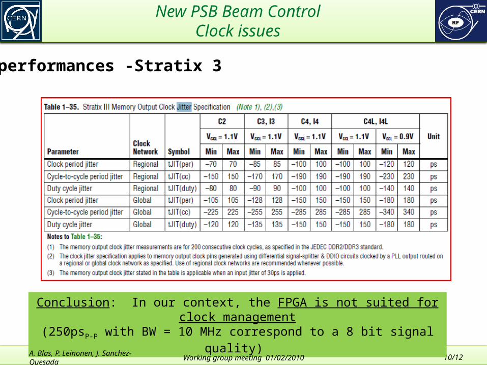
FPGA performances -Stratix 3
Conclusion: In our context, the FPGA is not suited for clock management(250psP-P with BW = 10 MHz correspond to a 8 bit signal quality)
A. Blas, P. Leinonen, J. Sanchez-Quesada Working group meeting 01/02/2010

New PSB Beam ControlClock issues
11/12
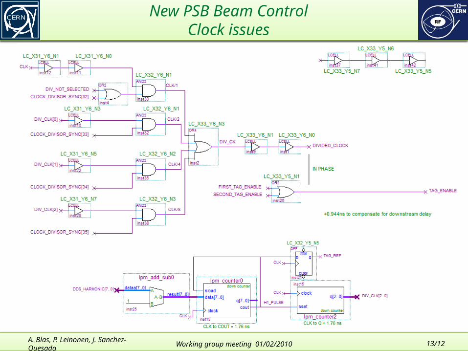
Clock and tag to be distributed
At 40 MHz, hclock = 4 => frf= 10 MHz, one clock period (25 ns) represents 90o of the rf phase.=> We do want to have an uncertainty in the acquisition of
the tag, to avoid 90o phase jumps in the feedback system
Þ Maximum tolerated skew between tag and clock = +/- 3ns The tag signal should be routed the same way as the clock
A. Blas, P. Leinonen, J. Sanchez-Quesada Working group meeting 01/02/2010
New PSB Beam ControlClock issues
12/12
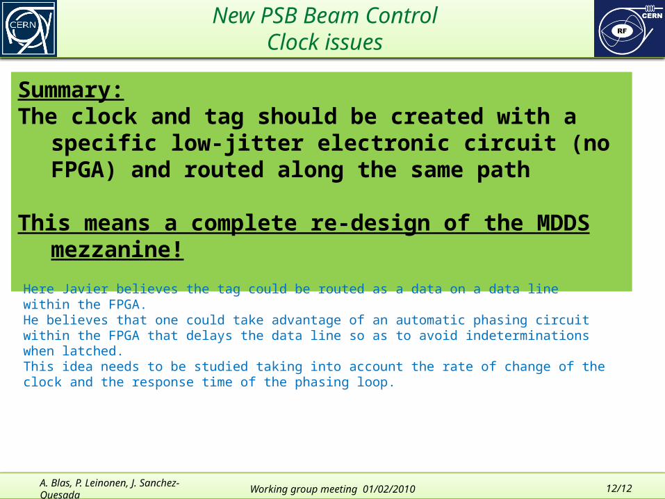
Summary:The clock and tag should be created with a specific low-jitter
electronic circuit (no FPGA) and routed along the same path
This means a complete re-design of the MDDS mezzanine!
A. Blas, P. Leinonen, J. Sanchez-Quesada Working group meeting 01/02/2010
Here Javier believes the tag could be routed as a data on a data line within the FPGA.He believes that one could take advantage of an automatic phasing circuit within the FPGA that delays the data line so as to avoid indeterminations when latched.This idea needs to be studied taking into account the rate of change of the clock and the response time of the phasing loop.
New PSB Beam ControlClock issues
13/12A. Blas, P. Leinonen, J. Sanchez-Quesada Working group meeting 01/02/2010

New PSB Beam ControlClock issues
14/12A. Blas, P. Leinonen, J. Sanchez-Quesada Working group meeting 01/02/2010
New PSB Beam ControlClock issues
15/12A. Blas, P. Leinonen, J. Sanchez-Quesada Working group meeting 01/02/2010
New PSB Beam ControlClock issues
A. Blas 16/12
tJtAtJtAtv
tJtAtv
ji
iji
i
ji
sin2
sincossin2
cossin)(
sin21sin)(
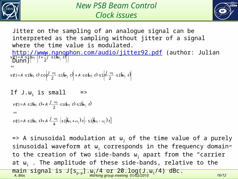
If J.ωi is small =>
ttJAtAtv
ttJAtAtv
jijii
i
jii
i
sinsin4
sin)(
sincos2
sin)(
=> A sinusoidal modulation at ωj of the time value of a purely sinusoidal waveform at ωi corresponds in the frequency domain to the creation of two side-bands ωj apart from the “carrier” at ωi . The amplitude of these side-bands, relative to the main signal is J[sp-p].ωi/4 or 20.log(J.ωi/4) dBc.
Jitter on the sampling of an analogue signal can be interpreted as the sampling without jitter of a signal where the time value is modulated. http://www.nanophon.com/audio/jitter92.pdf (author: Julian Dunn)
Working group meeting 01/02/2010
New PSB Beam ControlClock issues
A. Blas Working group meeting 18/09/2009 17/12
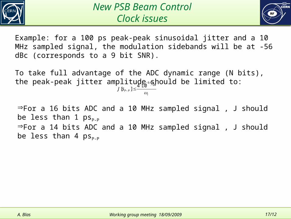
Example: for a 100 ps peak-peak sinusoidal jitter and a 10 MHz sampled signal, the modulation sidebands will be at -56 dBc (corresponds to a 9 bit SNR).
To take full advantage of the ADC dynamic range (N bits), the peak-peak jitter amplitude should be limited to:
i
N
PPsJ
206
104][
ÞFor a 16 bits ADC and a 10 MHz sampled signal , J should be less than 1 psP-P ÞFor a 14 bits ADC and a 10 MHz sampled signal , J should be less than 4 psP-P
New PSB Beam ControlClock issues
A. Blas Working group meeting 18/09/2009 18/12
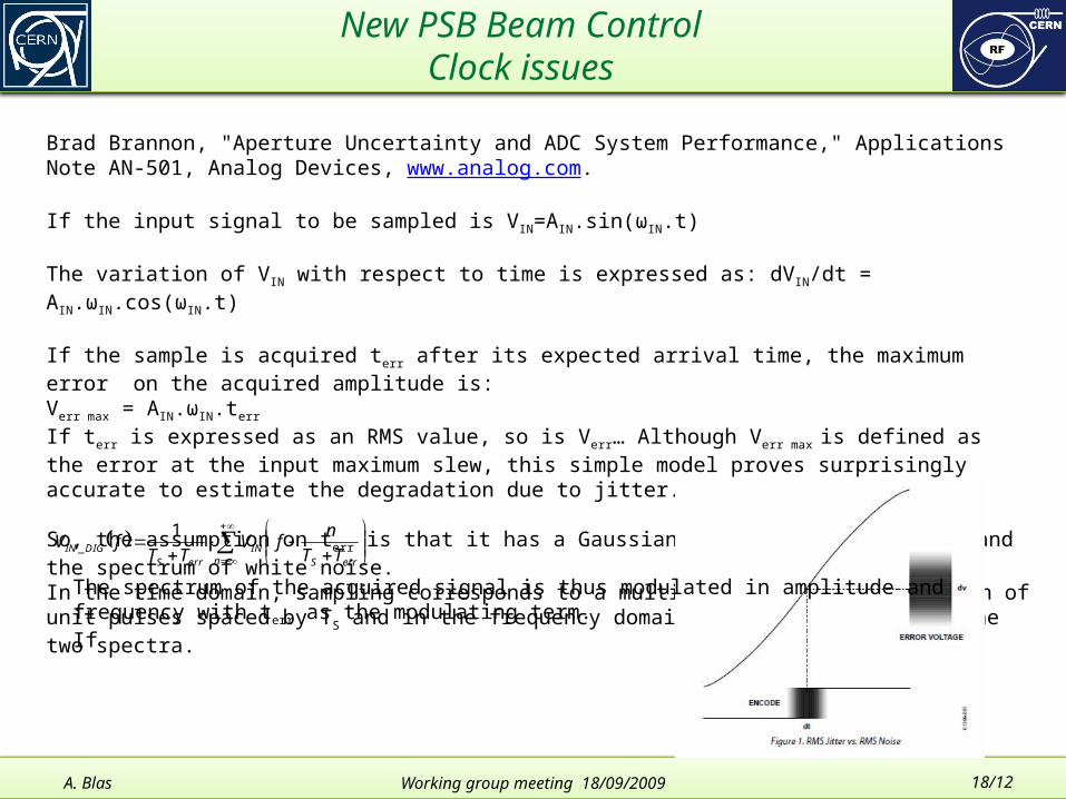
Brad Brannon, "Aperture Uncertainty and ADC System Performance," Applications Note AN-501, Analog Devices, www.analog.com.
If the input signal to be sampled is VIN=AIN.sin(ωIN.t)
The variation of VIN with respect to time is expressed as: dVIN/dt = AIN.ωIN.cos(ωIN.t)
If the sample is acquired terr after its expected arrival time, the maximum error on the acquired amplitude is:Verr max = AIN.ωIN.terr
If terr is expressed as an RMS value, so is Verr… Although Verr max is defined as the error at the input maximum slew, this simple model proves surprisingly accurate to estimate the degradation due to jitter.
So, the assumption on terr is that it has a Gaussian amplitude distribution and the spectrum of white noise.In the time domain, sampling corresponds to a multiplication by a succession of unit pulses spaced by TS and in the frequency domain, to a convolution of the two spectra.
n errS
INerrS
DIGIN TTnfV
TTfV 1
_
The spectrum of the acquired signal is thus modulated in amplitude and frequency with terr as the modulating term.If
New PSB Beam ControlClock issues
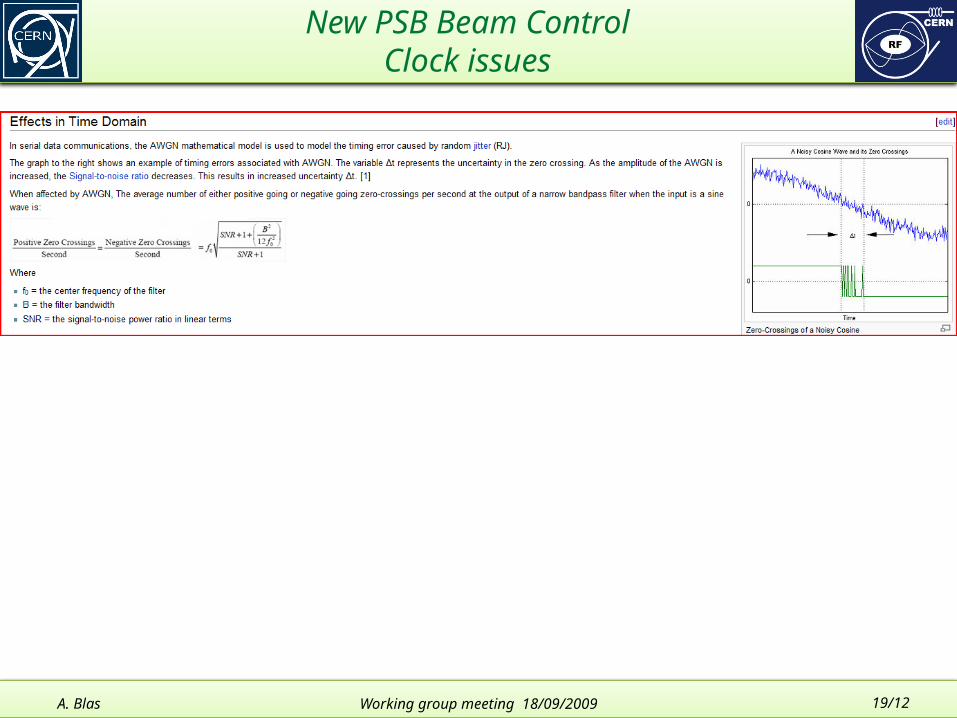
A. Blas Working group meeting 18/09/2009 19/12
New PSB Beam ControlClock issues
A. Blas Working group meeting 18/09/2009 20/12
1. FPGA performances
Many of the traditional methods manufacturers use to specify clock jitter do not apply to data converters or, at best, reveal only a fraction of the story. It is important that you know the bandwidth and spectral shape of the clock noise so that you can properly account for them during sampling. picoseconds of clock jitter quickly translate to decibels lost in the signal path.Many trade-offs relate to jitter, phase-noise, and converter performanceIt is difficult to provide a direct correlation between clock jitter and phase noise, but some guidelines exist for designing or selecting encoding sources from either a clock-jitter or a phase-noise perspective. Random jitter is characteristically gaussian; the rms time value or standard deviation of the occurrences specifies this random jitter. When considering the bandwidth of the noise that constitutes jitter for a data converter, the range is from dc to the encoding bandwidth, which exceeds far beyond the typical 12 kHz to 20 MHz that vendors often quote for standard clock-jitter measurements. Because the concern with jitter is increased wideband-converter noise, it is easy to estimate clock jitter by observing the degradation in noise performance of a converter. Equation 1 defines the SNR limitation due to jitter: EQUATION 1SNR=-20log(2.pi.fanalog.tjitterRMS)dBwhere f is the analog input frequency and t is the jitter. Solving this equation for t puts it in the form of Equation 2, which defines the clock-jitter requirement, given a frequency of operation and an SNR requirement:
log
20
210
ana
SNR
jitter ft
=> Can we use an FPGA as a clock gating unit?
New PSB Beam ControlClock issues
A. Blas Working group meeting 18/09/2009 21/12
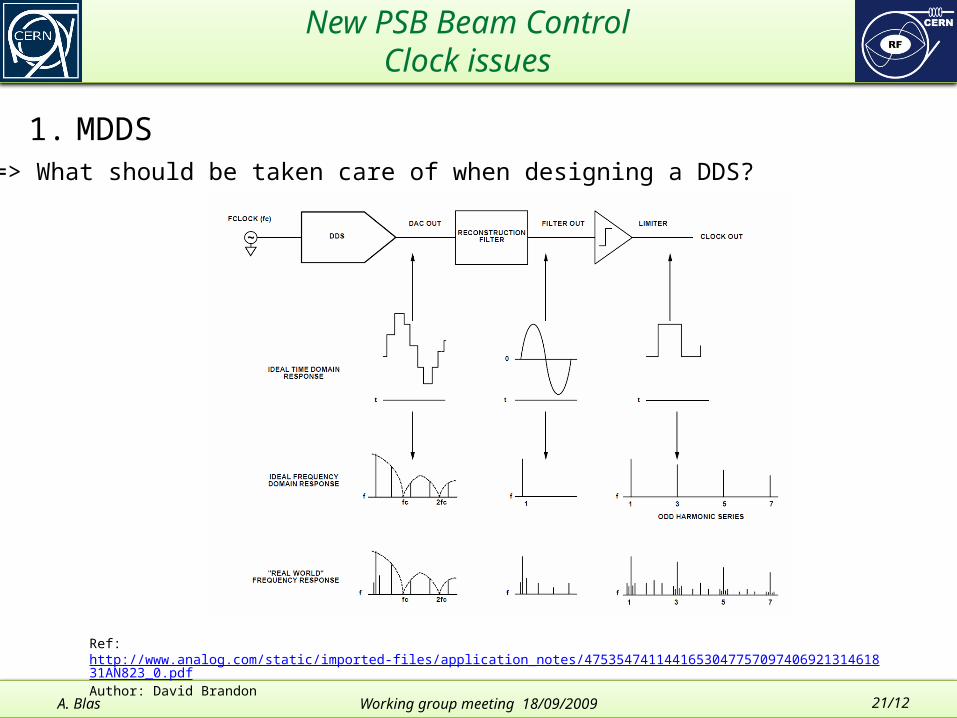
1. MDDS
Ref:http://www.analog.com/static/imported-files/application_notes/475354741144165304775709740692131461831AN823_0.pdfAuthor: David Brandon
=> What should be taken care of when designing a DDS?
New PSB Beam ControlClock issues
A. Blas Working group meeting 18/09/2009 22/12
1. MDDS=> To minimize noise coupling, it is advantageous to have a 2-wire, balanced connection between the DAC output and the limiter input. the real-world spectrum of an unfiltered DDS output is rich in spurious content. It contains DAC related harmonic distortion as well as the images of the fundamental Frequency. The images of the fundamental reside above the cutoff frequencyof the reconstruction filter. However, the harmonics of the fundamental are also reproduced in the images. Images that extend into the 1st Nyquist zone (DC to ½ fc), appear as aliased versions of the harmonics. Thus, the images may appear within the filter pass band. These in band images of the DAC harmonics as well as out-of-band images not sufficiently attenuated by the filter can contribute significantly to the jitter observed on the output of the limiter The jitter present at the output of the limiter is due to spur-induced, cycle-to-cycle, modulation of the time interval at which the limiter threshold voltage is crossed. The jitter that is generated by this process is classified as deterministic jitter; it is related to the specific frequencies of the spurious content of the signal. The process of spurious components being converted to a phase, or timing error (jitter) via the limiting function is referred to as AM to PM conversion. If the bandwidth of the filter is reduced, either by using a low-pass filter with a reduced cutoff frequency, or a band-pass filter, the amount of spurious noise is reduced. Bandwidth limiting this spurious noise in turn reduces the magnitude of time jitter that is produced. The magnitude of the time jitter produced is proportional to the magnitude of the spurious components with respect to the slew rate of the fundamental signal. Noise coupling between the DAC output and the limiter input, including device noise from the limiter itself, can also contribute to increased jitter. In general, increased slew rate at the input to a limiter translates to less sensitivity to jitter induced by coupled noise. Because slew rate is proportional to frequency and amplitude, an increase in either parameter tends to improve jitter performance.The key points in minimizing jitter in DDS-based clock systems are maximizing the DAC output slew rate and implementing effective filtering of the DDS spurious components
New PSB Beam ControlClock issues
A. Blas Working group meeting 18/09/2009 23/12
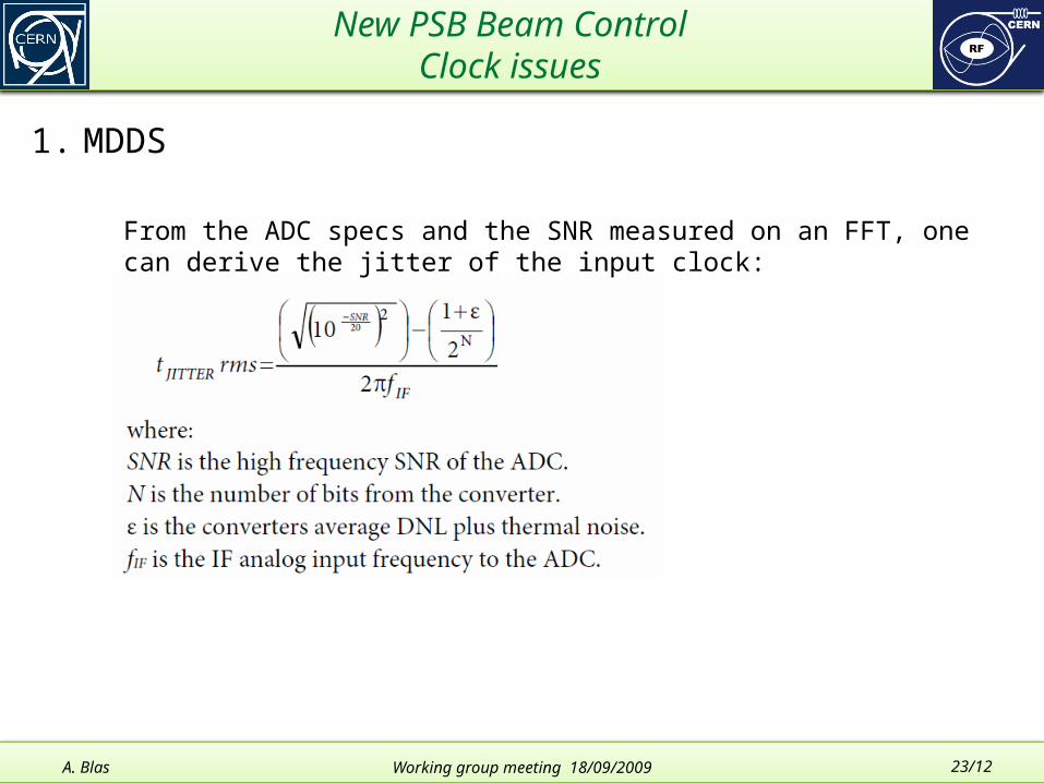
1. MDDS
From the ADC specs and the SNR measured on an FFT, one can derive the jitter of the input clock:
New PSB Beam ControlClock issues
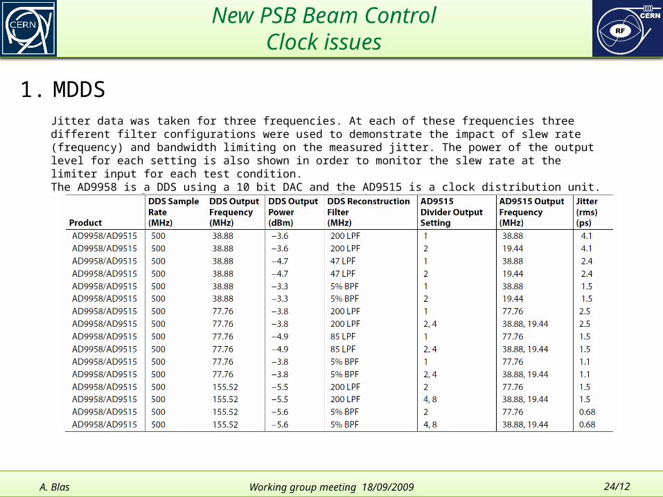
A. Blas Working group meeting 18/09/2009 24/12
1. MDDSJitter data was taken for three frequencies. At each of these frequencies three different filter configurations were used to demonstrate the impact of slew rate (frequency) and bandwidth limiting on the measured jitter. The power of the output level for each setting is also shown in order to monitor the slew rate at the limiter input for each test condition.The AD9958 is a DDS using a 10 bit DAC and the AD9515 is a clock distribution unit.
New PSB Beam ControlClock issues
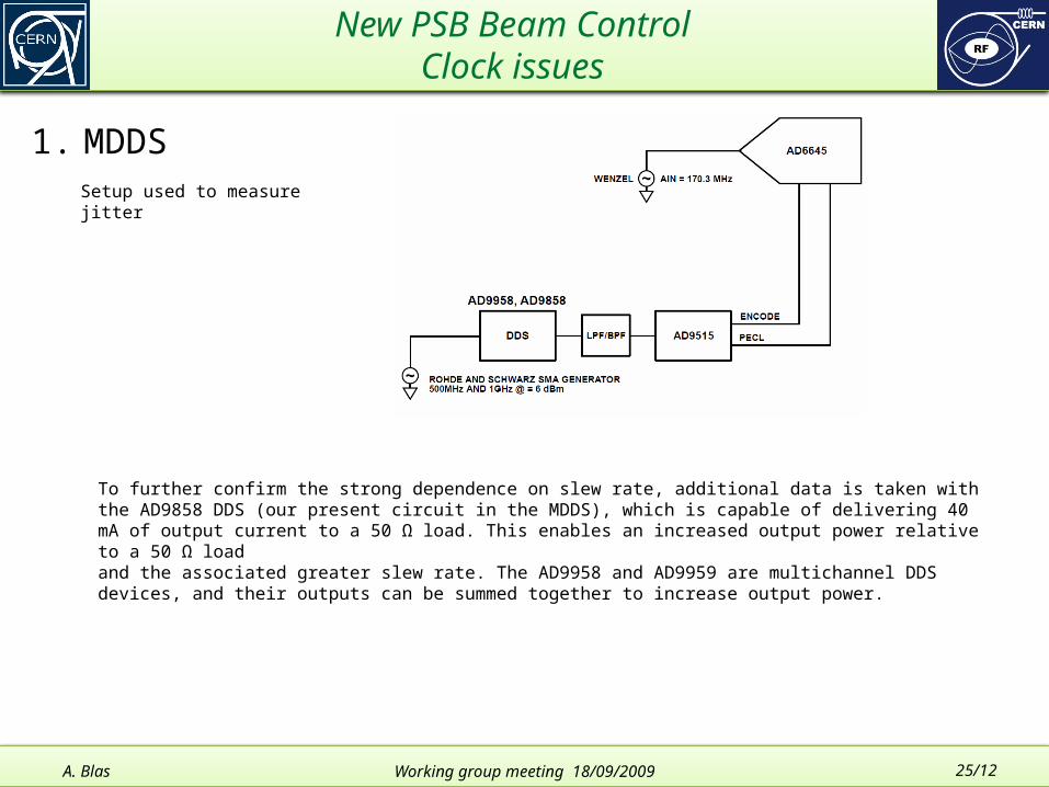
A. Blas Working group meeting 18/09/2009 25/12
1. MDDSSetup used to measure jitter
To further confirm the strong dependence on slew rate, additional data is taken with the AD9858 DDS (our present circuit in the MDDS), which is capable of delivering 40 mA of output current to a 50 Ω load. This enables an increased output power relative to a 50 Ω loadand the associated greater slew rate. The AD9958 and AD9959 are multichannel DDS devices, and their outputs can be summed together to increase output power.
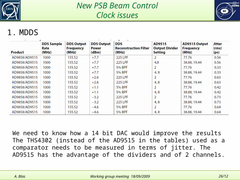
New PSB Beam ControlClock issues
A. Blas Working group meeting 18/09/2009 26/12
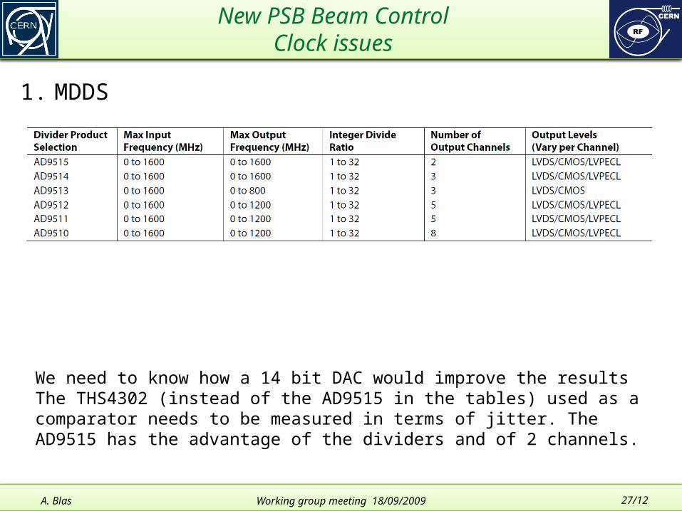
1. MDDS
We need to know how a 14 bit DAC would improve the resultsThe THS4302 (instead of the AD9515 in the tables) used as a comparator needs to be measured in terms of jitter. The AD9515 has the advantage of the dividers and of 2 channels.
New PSB Beam ControlClock issues
A. Blas Working group meeting 18/09/2009 27/12
1. MDDS
We need to know how a 14 bit DAC would improve the resultsThe THS4302 (instead of the AD9515 in the tables) used as a comparator needs to be measured in terms of jitter. The AD9515 has the advantage of the dividers and of 2 channels.