
Nanowire-Based Sublithographic Programmable Logic...
14
Extended Version with Detail Appendix <http://www.cs.caltech.edu/research/ic/abstracts/nanopla_fpga2004.html> Nanowire-Based Sublithographic Programmable Logic Arrays Andr ´ e DeHon Dept. of CS, 256-80 California Institute of Technology Pasadena, CA 91125 [email protected] Michael J. Wilson Dept. of CS, 256-80 California Institute of Technology Pasadena, CA 91125 [email protected] ABSTRACT How can Programmable Logic Arrays (PLAs) be built with- out relying on lithography to pattern their smallest fea- tures? In this paper, we detail designs which exploit emerg- ing, bottom-up material synthesis techniques to build PLAs using molecular-scale nanowires. Our new designs accom- modate technologies where the only post-fabrication pro- grammable element is a non-restoring diode. We introduce stochastic techniques which allow us to restore the diode logic at the nanoscale so that it can be cascaded and in- terconnected for general logic evaluation. Under conserva- tive assumptions using 10nm nanowires and 90nm litho- graphic support, we project yielded logic density around 500,000nm 2 /or term for a 60 or-term array; a complete 60-term, two-level PLA is roughly the same size as a sin- gle 4-LUT logic block in 22nm lithography. Each or term is comparable in area to a 4-transistor hardwired gate at 22nm. Mapping sample datapaths and conventional programmable logic benchmarks, we estimate that each 60-or-term PLA plane will provide equivalent logic to 5–10 4-input LUTs. Categories and Subject Descriptors B.6.1 [Logic Design]: Design Styles—logic arrays ; B.7.1 [Integrated Circuits]: Types and Design Styles—advanced technologies General Terms Design Keywords Sublithographic architecture, nanowires, programmable logic arrays 1. INTRODUCTION Programmable logic arrays (PLAs) have been a child of lithography. Before lithographic integrated circuits, it did Permission to make digital or hard copies of all or part of this work for personal or classroom use is granted without fee provided that copies are not made or distributed for profit or commercial advantage and that copies bear this notice and the full citation on the first page. To copy otherwise, to republish, to post on servers or to redistribute to lists, requires prior specific permission and/or a fee. FPGA’04, February 22-24, 2004, Monterey, California, USA. Copyright 2004 ACM 1-58113-829-6/04/0002 ...$5.00. not make sense to build PLAs; logic was “customized” by discrete wiring (e.g. patch cables). Once lithography could support enough logic on a single chip to accommodate pro- grammable configuration elements, it became interesting and useful to include memory elements which could configure the state of the device. As a result we developed PALs, PLDs, and ultimately FPGAs. Now it is becoming possible to look beyond lithography and explore how we can build devices without relying on lithography to pattern our smallest feature sizes. Scientists are demonstrating bottom up techniques for defining key feature sizes. These techniques suggest a path to molecular- scale dimensions—they show us how to build features which are just a few atoms across. At this scale, programmable elements may be necessary in order to build any logic. In this paper, we explore how to use nanowires (NWs) to build sublithographic PLAs and interconnected PLAs. These PLA blocks are likely to form leaf clusters in large- scale, sublithographic programmable logic devices just as small PLAs form leaf clusters in conventional, “complex” PLDs. Owing to the fabrication regularity demanded when using bottom-up techniques, the leaf clusters, and even the programmable interconnect, are likely to be engineered and parameterized quite differently from today’s, lithographic- scale CPLDs. We identify those issues and explore where the technology limitations and costs drive our designs. We build a two-plane PLA with decorated silicon NWs (See Figure 1). The NWs serve as our primary interconnect and device building block (Section 2.1). We build upon pro- grammable crosspoint diodes (Section 2.2). We show that we can address individual NWs from the lithographic scale which is necessary for bootstrap programming (Section 2.3). We show how we achieve restoring logic and connect that to the programmable diode logic (Section 3), and we detail a precharge clocking scheme for logic evaluation (Section 4). We show how the basic PLA cycle can be embellished to al- low PLA evaluation through a configurable number of logic planes (Section 5). We calculate the area, timing, and yield of these devices (Section 6) and sketch the discovery of the basic state of the devices to enable configuration and defect avoidance (Section 7). Finally, we map small, conventional programmable logic benchmarks and a select set of datap- aths onto these devices to estimate their effective density compared to conventional alternatives (Section 8). New contributions of this work include: • explicit formulation of NW-based PLAs with separate pro- grammable and restoring devices
-
Upload
truongngoc -
Category
Documents
-
view
241 -
download
0
Transcript of Nanowire-Based Sublithographic Programmable Logic...
Extended Version with Detail Appendix <http://www.cs.caltech.edu/research/ic/abstracts/nanopla_fpga2004.html>
Nanowire-Based SublithographicProgrammable Logic Arrays
Andre DeHonDept. of CS, 256-80
California Institute of TechnologyPasadena, CA 91125
Michael J. WilsonDept. of CS, 256-80
California Institute of TechnologyPasadena, CA 91125
ABSTRACTHow can Programmable Logic Arrays (PLAs) be built with-out relying on lithography to pattern their smallest fea-tures? In this paper, we detail designs which exploit emerg-ing, bottom-up material synthesis techniques to build PLAsusing molecular-scale nanowires. Our new designs accom-modate technologies where the only post-fabrication pro-grammable element is a non-restoring diode. We introducestochastic techniques which allow us to restore the diodelogic at the nanoscale so that it can be cascaded and in-terconnected for general logic evaluation. Under conserva-tive assumptions using 10nm nanowires and 90nm litho-graphic support, we project yielded logic density around500,000nm2/or term for a 60 or-term array; a complete60-term, two-level PLA is roughly the same size as a sin-gle 4-LUT logic block in 22nm lithography. Each or term iscomparable in area to a 4-transistor hardwired gate at 22nm.Mapping sample datapaths and conventional programmablelogic benchmarks, we estimate that each 60-or-term PLAplane will provide equivalent logic to 5–10 4-input LUTs.
Categories and Subject DescriptorsB.6.1 [Logic Design]: Design Styles—logic arrays; B.7.1[Integrated Circuits]: Types and Design Styles—advancedtechnologies
General TermsDesign
KeywordsSublithographic architecture, nanowires, programmable logicarrays
1. INTRODUCTIONProgrammable logic arrays (PLAs) have been a child of
lithography. Before lithographic integrated circuits, it did
Permission to make digital or hard copies of all or part of this work forpersonal or classroom use is granted without fee provided that copies arenot made or distributed for profit or commercial advantage and that copiesbear this notice and the full citation on the first page. To copy otherwise, torepublish, to post on servers or to redistribute to lists, requires prior specificpermission and/or a fee.FPGA’04,February 22-24, 2004, Monterey, California, USA.Copyright 2004 ACM 1-58113-829-6/04/0002 ...$5.00.
not make sense to build PLAs; logic was “customized” bydiscrete wiring (e.g. patch cables). Once lithography couldsupport enough logic on a single chip to accommodate pro-grammable configuration elements, it became interesting anduseful to include memory elements which could configure thestate of the device. As a result we developed PALs, PLDs,and ultimately FPGAs.
Now it is becoming possible to look beyond lithographyand explore how we can build devices without relying onlithography to pattern our smallest feature sizes. Scientistsare demonstrating bottom up techniques for defining keyfeature sizes. These techniques suggest a path to molecular-scale dimensions—they show us how to build features whichare just a few atoms across. At this scale, programmableelements may be necessary in order to build any logic.
In this paper, we explore how to use nanowires (NWs)to build sublithographic PLAs and interconnected PLAs.These PLA blocks are likely to form leaf clusters in large-scale, sublithographic programmable logic devices just assmall PLAs form leaf clusters in conventional, “complex”PLDs. Owing to the fabrication regularity demanded whenusing bottom-up techniques, the leaf clusters, and even theprogrammable interconnect, are likely to be engineered andparameterized quite differently from today’s, lithographic-scale CPLDs. We identify those issues and explore wherethe technology limitations and costs drive our designs.
We build a two-plane PLA with decorated silicon NWs(See Figure 1). The NWs serve as our primary interconnectand device building block (Section 2.1). We build upon pro-grammable crosspoint diodes (Section 2.2). We show thatwe can address individual NWs from the lithographic scalewhich is necessary for bootstrap programming (Section 2.3).We show how we achieve restoring logic and connect that tothe programmable diode logic (Section 3), and we detail aprecharge clocking scheme for logic evaluation (Section 4).We show how the basic PLA cycle can be embellished to al-low PLA evaluation through a configurable number of logicplanes (Section 5). We calculate the area, timing, and yieldof these devices (Section 6) and sketch the discovery of thebasic state of the devices to enable configuration and defectavoidance (Section 7). Finally, we map small, conventionalprogrammable logic benchmarks and a select set of datap-aths onto these devices to estimate their effective densitycompared to conventional alternatives (Section 8).
New contributions of this work include:• explicit formulation of NW-based PLAs with separate pro-
grammable and restoring devices

Ohmic contacts to high and low supply voltages
nanowires
programmablediode crosspoints Lightly doped
control region
Precharge or static load devices
Stochastic Buffer Array
(Sec 2.2)
Stochastic Inversion Array(Sec 3)
(Sec 2.1)
Vrow1
Vrow2
A0 A1 A2 A3
Lightly dopedcontrol region
(OR Planes)
Stochastic Address Decoder (Sec 2.3)[for configuring array]
OR term
Restoration Wire
OhmicContactto PowerSupply
Programingand PrechargePower Suppplies
Stochastic Inversion Array(Sec 3)
Stochastic Buffer Array
Restoration Columns Restoration Columns
Ohmic contactsto high and lowsupply voltages
Figure 1: Simple Nanowire PLA Composition
• introduction of stochastic techniques for building fixed,restoring logic
• introduction of a PLA topology which requires lithographicprogramming lines in only one dimension and allows pro-gramming to be shared across multiple arrays
• introduction of a clocked, precharge scheme for sublitho-graphic PLA logic
• introduction of simple topologies for physically config-urable PLA cycles
• estimation of net logic density using mapped logic in-stances from both standard programmable logic bench-marks and focused datapath elements
2. BACKGROUND
2.1 NanowiresSemiconducting nanowires (NWs) can be grown to con-
trolled dimensions on the nanometer scale using seed cata-lysts (e.g. gold balls) to define their diameter. NWs withdiameters down to 3nm have been demonstrated [9] [31].By controlling the mix of elements in the environment dur-ing growth, semiconducting NWs can be doped to controltheir electrical properties [8]. Conduction through dopedNWs can be controlled via an electrical field like Field-EffectTransistors (FETs) [21]. The doping profile along the lengthof a NW can be controlled by varying the dopant level in thegrowth environment over time [18]; as a result, our controlover growth rate allows us to control the physical dimensionsof these features down to almost atomic precision. The dop-ing profile can also be controlled along the radius of theseNWs, allowing us to sheath NWs in insulators (e.g. silicon-dioxide) [26] to control spacing between conductors [38] andbetween gated wires and control wires.
Flow techniques can be used to align a set of NWs into asingle orientation, close pack them, and transfer them ontoa surface [22] [38]. This step can be rotated and repeated sothat we get multiple layers of NWs [22] [39] such as crossedNWs for building a crossbar array or memory core.
Each of the capabilities described above has been demon-strated in a lab setting as detailed in the papers cited. Weassume it will be possible to combine these capabilities andscale them into a repeatable manufacturing process.
2.2 Programmable Diode CrosspointsOver the past few years, many technologies have been
demonstrated for molecular-scale memories. So far, theyall seem to have: (1) resistance which changes significantlybetween “on” and “off” states, (2) the ability to be maderectifying, and (3) the ability to turn the device “on” or“off” by applying a voltage differential across the junction.Rueckes et. al. demonstrate switched devices using sus-pended nanotubes to realize a bistable junction with an en-ergy barrier between the two states [34]. In the “off” statethe junction exhibits only small tunneling current (high re-sistance ∼GΩs); when the devices are in contact in the “on”state, there is little resistance (∼100KΩ) between the tubes.UCLA and HP have demonstrated a number of moleculeswhich exhibits hysteresis [5] [6]. HP has demonstrated an8×8 crossbar made from [2]rotaxane molecules and observedthat they could force an order of magnitude resistance dif-ference between “on” and “off” state junctions [3].
2.3 Addressing Nanowires from LithographicScale Wires
The preceding technologies allow us to pack NWs at atight pitch into crossbars with programmable crosspoints attheir junctions. The pitch of the NWs can be much smallerthan our lithographic patterning. We will be using the cross-point programmability to configure logic functions into ournanoscale devices. In order to do this, we need a way to se-lectively place a defined voltage on a single row and columnwire in order to set the state of the crosspoint.
By constructing NWs with doping profiles on their ends,we can give each NW an address (See left end of Figure 1).The dimensions of the address bit control regions can beset to the lithographic pitch so that a set of crossed, litho-graphic wires can be used to address a single NW. If wecode up all the NWs along one dimension of an array withsuitably different codes, we can get unique NW address-ability and effectively implement a demultiplexer betweena small number of lithographic wires and a large numberof NWs. We cannot control exactly which NW codes ap-pear in a single array or how they are aligned, but if werandomly select NWs from a sufficiently large code space,we will achieve uniqueness with very high probability (over
99% easily achievable). The addresses do not have to beentirely unique for this application; allowing a little redun-dancy will allow us to use a tighter code space. The basicstochastic addressing scheme is developed in detail in [14].Calculations allowing redundancy are summarized in [15].
2.4 Technology RoundupWe can create wires which are nanometers in diameter
and can be arranged into crossbar arrays with nanometerpitch. Crosspoints which both switch conduction betweenthe crossed wires and store their own state can be placed atevery wire crossing without increasing the pitch of the cross-bar array. NWs can be controlled in FET-like manner andcan be designed with selectively gateable regions. The NWscan be individually addressed from the lithographic scale.No lithography is required to define the nanoscale featuresin the crossbar; lithography is used to define the extents ofthe crossbar, provide addressing for bootstrap programming,and provide voltage supplies for the NW array.
2.5 Related WorkSeveral researchers have begun to explore programmable
logic structures at this scale. Heath [20] articulates a visionfor this kind of molecular-scale logic. Goldstein’s nanoFab-rics [16] are a possible implementation of this vision usingonly the two-terminal diode crosspoints introduced above.Tour’s nanoCell [37] employs a random network of config-urable Negative Differential Resistance (NDR), avoiding theneed for carefully ordered conductors on the nanoscale butstill requiring lithographic scale wires to interconnect andrestore nanoCells. Niemier [32] suggests an FPGA basedon Quantum Cellular Automata (QCA) which may requirelithographic-scale wires to control clock domains. NWs giveus unique capabilities currently not exploited in other ef-forts. The techniques introduced here elaborate and com-plement the parallel research efforts, demonstrating what wecan build with NWs, NW field-effect gating, doping profileson NWs, and stochastic population.
3. RESTORATIONProgrammable diode crosspoints in a crossbar array give
us a programmable or plane (See marked regions in Fig-ure 1). Each output NW in the plane can be programmedto perform the or of its set of inputs. That is, there is alow resistance path between the inputs and the output NWonly where the crosspoints are programmed into the “on”position. If any of those inputs are high, they will be ableto deliver current through the “on” crosspoint and pull theoutput line to a high value.
3.1 Limits of Diode LogicDiodes alone do not give us arbitrary or cascadable logic.
We know that or gates are not universal logic buildingblocks. With diodes alone we cannot invert signals whichwill be necessary to realize arbitrary logic. Further, when-ever an input is used by multiple outputs, we divide thecurrent among the outputs; this cannot continue througharbitrary stages as it will eventually not be possible to dis-tinguish the divided current from the leakage current of an“off” crosspoint. The diode junction may further providea voltage drop at every crosspoint such that the maximumoutput high voltage drops at every stage.
InputOutput
Rxpoint
(can be strong)
(weak) (weak)
Inverting Restore
Vpd (/precharge)
Vpu (/eval)
from otherbuffers orinverters
Vpd(precharge)
Input Output
Rxpoint
(weak)
precharge
Non−Inverting Restore
Vpd (/precharge)
Vpu (/eval)
from otherbuffers orinverters
(can be strong)
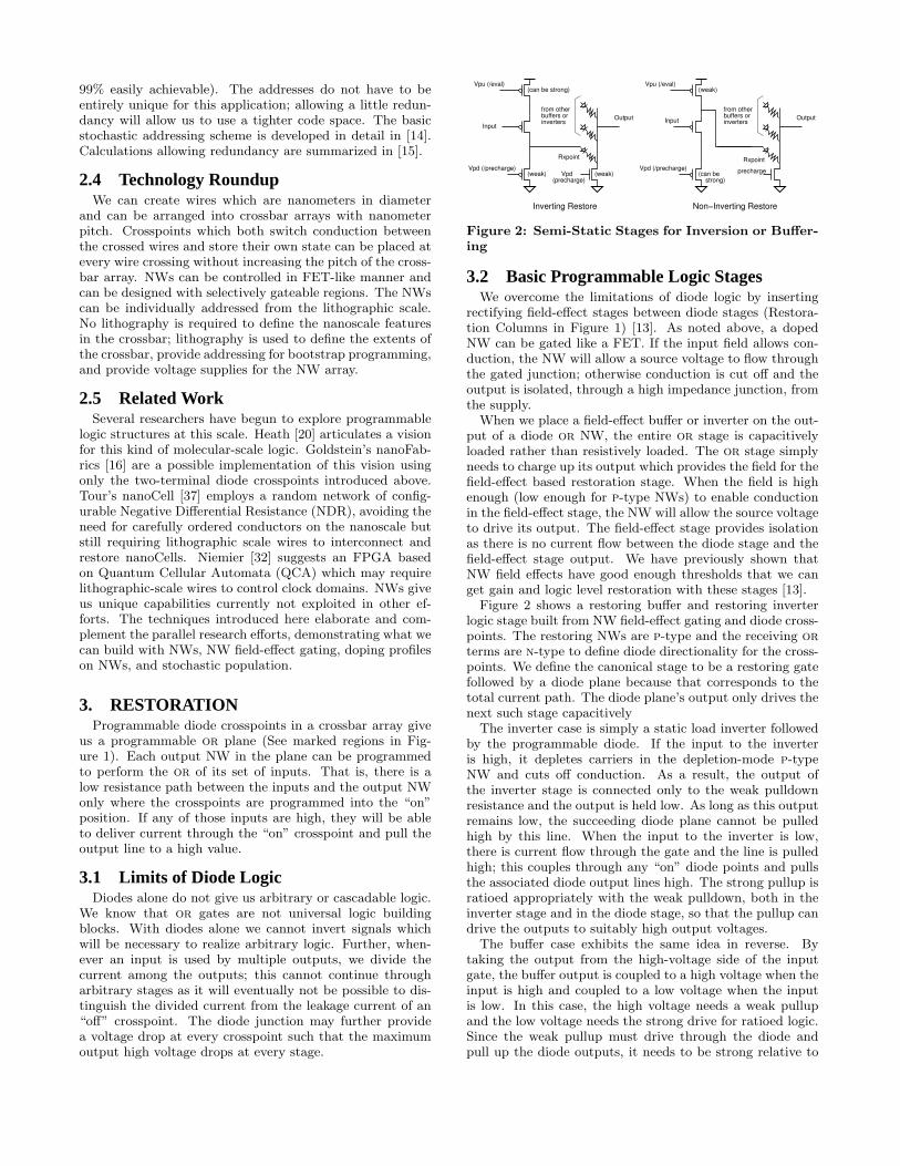
Figure 2: Semi-Static Stages for Inversion or Buffer-ing
3.2 Basic Programmable Logic StagesWe overcome the limitations of diode logic by inserting
rectifying field-effect stages between diode stages (Restora-tion Columns in Figure 1) [13]. As noted above, a dopedNW can be gated like a FET. If the input field allows con-duction, the NW will allow a source voltage to flow throughthe gated junction; otherwise conduction is cut off and theoutput is isolated, through a high impedance junction, fromthe supply.
When we place a field-effect buffer or inverter on the out-put of a diode or NW, the entire or stage is capacitivelyloaded rather than resistively loaded. The or stage simplyneeds to charge up its output which provides the field for thefield-effect based restoration stage. When the field is highenough (low enough for p-type NWs) to enable conductionin the field-effect stage, the NW will allow the source voltageto drive its output. The field-effect stage provides isolationas there is no current flow between the diode stage and thefield-effect stage output. We have previously shown thatNW field effects have good enough thresholds that we canget gain and logic level restoration with these stages [13].
Figure 2 shows a restoring buffer and restoring inverterlogic stage built from NW field-effect gating and diode cross-points. The restoring NWs are p-type and the receiving orterms are n-type to define diode directionality for the cross-points. We define the canonical stage to be a restoring gatefollowed by a diode plane because that corresponds to thetotal current path. The diode plane’s output only drives thenext such stage capacitively
The inverter case is simply a static load inverter followedby the programmable diode. If the input to the inverteris high, it depletes carriers in the depletion-mode p-typeNW and cuts off conduction. As a result, the output ofthe inverter stage is connected only to the weak pulldownresistance and the output is held low. As long as this outputremains low, the succeeding diode plane cannot be pulledhigh by this line. When the input to the inverter is low,there is current flow through the gate and the line is pulledhigh; this couples through any “on” diode points and pullsthe associated diode output lines high. The strong pullup isratioed appropriately with the weak pulldown, both in theinverter stage and in the diode stage, so that the pullup candrive the outputs to suitably high output voltages.
The buffer case exhibits the same idea in reverse. Bytaking the output from the high-voltage side of the inputgate, the buffer output is coupled to a high voltage when theinput is high and coupled to a low voltage when the inputis low. In this case, the high voltage needs a weak pullupand the low voltage needs the strong drive for ratioed logic.Since the weak pullup must drive through the diode andpull up the diode outputs, it needs to be strong relative to
Gnd
Vhigh
Programmable OR plane
Inputs toOR plane
OR Outputs
Vpd (/prechargeA)
Vpu (/evalA)
InvertedRestoredOutputs
Fixed InversionPlane
Lightly DopedFET ControllableRegion
Ohmic Contact to Voltage Source
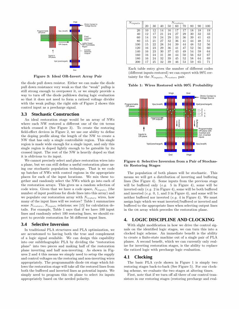
Figure 3: Ideal OR-Invert Array Pair
the diode pull down resistor. Either we can make the diodepull down resistance very weak so that the “weak” pullup isstill strong enough to overpower it, or we simply provide away to turn off the diode pulldown during logic evaluationso that it does not need to form a ratioed voltage dividerwith the weak pullup; the right side of Figure 2 shows thiscontrol input as a precharge signal.
3.3 Stochastic ConstructionAn ideal restoration stage would be an array of NWs
where each NW restored a different one of the or termswhich crossed it (See Figure 3). To create the restoringfield-effect devices in Figure 2, we use our ability to definethe doping profile along the length of the NW to create aNW that has only a single controllable region. This singleregion is made wide enough for a single input, and only thissingle region is doped lightly enough to be gateable by itscrossed input. The rest of the NW is heavily doped so thatit is oblivious to its input.
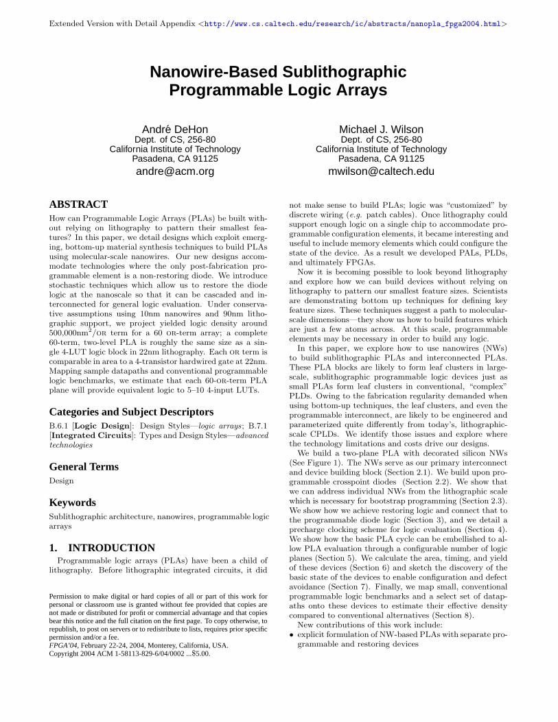
We cannot precisely select and place restoration wires intoa plane, but we can still define a useful restoration plane us-ing our stochastic population technique. That is we codeup batches of NWs with control regions in the appropriateplaces for each of the input locations. We mix these to-gether and randomly select the NWs which go into each ofthe restoration arrays. This gives us a random selection ofcode wires. Given that we have a code space, Ninputs, (thenumber of input positions for diode lines into this array) andwe populate our restoration array with Nrestore wires, howmany of the input lines will we restore? Table 1 summarizessome Nrestore, Ninputs relations; see [15] for calculation de-tails. For example, Table 1 says that if we have 100 inputlines and randomly select 100 restoring lines, we should ex-pect to provide restoration for 56 different input lines.
3.4 Selective InversionIn traditional PLA structures and PLA optimization, we
are accustomed to having both the true and complementof a logic signal available. We can design this capabilityinto our sublithographic PLA by dividing the “restorationplane” into two pieces and making half of the restorationplane inverting and half non-inverting. As shown in Fig-ures 2 and 4 this means we simply need to setup the supplyand control voltages on the restoring and non-inverting wiresappropriately. The programmable diode or stage which fol-lows the restoration stage will take all the restored lines fromboth the buffered and inverted lines as potential inputs. Wesimply need to program this or plane to select its inputsappropriately based on the needed polarity.
Ninputs Nrestore
20 30 40 50 60 70 80 90 100
20 10 12 14 16 17 17 18 18 1940 12 17 21 24 27 29 30 32 3360 14 19 24 29 33 36 39 41 4380 15 21 27 32 36 41 44 48 51
100 15 22 28 34 39 44 48 52 56120 16 23 29 36 41 47 52 56 60140 16 23 30 37 43 49 54 59 64160 16 24 31 38 44 50 56 62 67180 16 24 32 39 45 52 58 64 69200 17 25 32 39 46 53 59 65 71
Each table entry gives the number of different codes(different inputs restored) we can expect with 99% cer-tainty for the Ninputs, Nrestore pair.
Table 1: Wires Restored with 99% Probability
ProgrammableOR plane withinverted andnon−invertedinputs
Vhigh
Programmable OR plane
Inputs toOR plane
Vpu(/evalA)
Gnd
OR outputs
Vpd(/prechargeA)
Gnd
Vpd(/prechargeA)
Vhigh
Vpu(/evalA)
Inverted
Buffered
01
23
45
Ohmic Contact toVoltage Source
Figure 4: Selective Inversion from a Pair of Stochas-tic Restoring Stages
The population of both planes will be stochastic. Thismeans we will get a distribution of inverting and bufferinglines (See Figure 4). Some inputs from the previous stagewill be buffered only (e.g. 5 in Figure 4), some will beinverted only (e.g. 2 in Figure 4), some will be both bufferedand inverted (e.g. 0, 1, and 3 in Figure 4), and some will beneither buffered nor inverted (e.g. 4 in Figure 4). We mustassign logic which we want inverted/buffered or inverted andbuffered to the appropriate lines when selecting output linesin the or array which precedes the restoration plane.
4. LOGIC DISCIPLINE AND CLOCKINGWith slight modification in how we drive the control sig-
nals on the identified logic stages, we can turn this into aclocked logic scheme. An immediate benefit is the abilityto create a finite-state machine out of a single pair of PLAplanes. A second benefit, which we can currently only real-ize for inverting restoration stages, is the ability to replacethe ratioed logic with precharge logic evaluation.
4.1 ClockingThe basic PLA cycle shown in Figure 1 is simply two
restoring stages back-to-back (See Figure 5). For our clock-ing scheme, we evaluate the two stages at altering times.
First, note that if we turn off all three of our control tran-sistors in our restoring stages (restoring precharge and eval-

Binv
BinputBout
/prechargeB
/evalB
prechargeB
/prechargeA
Ainv
Ainput Aout
/evalA
prechargeA
otherinputs
otherinputs
Figure 5: Precharge Clocked INV-OR-INV-OR(nand-nand, nor-nor, and-or) Cycle
prechargeA
evalA
Arestore
Aout
prechargeB
evalB
Brestore
Bout
Ain stable
new valueold
new valueold
Bin stable
new valueold
new valueold
Tplacycle
Tpre Tno Teval Tpre Tno Teval TbaTab
Figure 6: Clocking/Precharge Timing Diagram
uate and diode precharge), there is no current path from theinput to the diode output stage. We effectively isolate theinput from the output. Since the output stage is capacitivelyloaded, the output will hold its value. As with any dynamicscheme, eventually leakage on the output will be an issue,which will set a lower bound on the clock frequency. Owingto the small charges, this lower bound will be higher in NWlogic than in conventional lithographic logic.
With a stage isolated and holding its output, we can evalu-ate the following stage. It computes its value from its input,the output of the previous stage, and produces its result bysuitably charging its output line. Once this is done, we canisolate this stage and evaluate its succeeding stage, which,in this simple case, is also its predecessor.
In this manner, we never have an open current path allthe way around the PLA (See Figure 5 and 6). In the twophases of operation, we effectively have a single register onany PLA outputs which feed back to PLA inputs.
4.2 Precharge EvaluationFor the inverting stage, we can dispense entirely with the
weak pulldown transistor. Instead, we drive the pulldowngate hard during precharge and turn it off during evaluation.In this manner, we precharge the line low and pull it uponly if the input is low. This works conveniently in this casebecause the output will also be precharged low. If the inputis high, then we do not want to pullup the output and simplyleave it low. If the input is low, we enable the current path topullup the output. The net benefit is that inverter pulldownand pullup are both controlled by strongly driven gates andcan be fast, whereas in the static logic scheme, the pulldown
IsolationDevicesPLA 1 PLA 2
Shared Address Decoder
Figure 7: Address Decoder Shared Across PLAs
transistor had to be weak, making pulldown slow comparedto pullup. Typically, the weak pulldown transistor wouldbe set to have an order of magnitude higher resistance thanthe pullup transistor, so this can be a significant reductionin worst-case gate evaluate latency (See Section 6.4).
Unfortunately, we can neither precharge to high nor turnoff the weak pullup resistor in the buffer case, so we do notget comparable benefits there. Perhaps new devices or cir-cuit organizations will eventually allow us to build prechargebuffer stages.
5. ORGANIZATIONThe two-level PLA is adequate to implement logic in two-
level sum-of-products form. Nonetheless, it is well knownthat many common functions require an exponential num-ber of product terms when forced to two-level form, whereasthey can be implemented in a linear number of gates (e.g.xor). Research on optimal PLA block size to include in con-ventional, lithographic FPGAs suggests PLA blocks containmodest (e.g. 10) product terms and programmable inter-connect [23]. However, the fact that we wish to amortizeout the lithographic programming lines to get the benefitsof sublithographic PLAs will likely shift the beneficial PLAsize to larger numbers of product terms.
Here we explore how we can spread PLA evaluation overmultiple planes to avoid unreasonable growth in productterm requirements. We focus on two options for spreadingout PLA evaluation and their interaction:1. physically creating PLA cycles with s stages2. looping the evaluation of some function w times through
a set of s stages
5.1 Simple Cycle OrganizationWhen we put together stochastic addressing, stochastic
inversion, programmable diode crosspoints, and prechargeclocking, we get a tight, two-plane array. This topologyrequires addressing overhead for programming only in oneof the two dimensions (See left side of Figure 1).
A second feature of this array and clocking scheme is thatthe row addresses can be shared among multiple such PLAplanes (See Figure 7). An isolation transistor serves to elec-trically separate the row segments of the planes during op-eration; during programming, the isolation transistor allowsthe row decoder to address all of the PLAs. The key featurewhich allows this sharing is that all rows on the same phasecan be pulled down simultaneously during their associatedprecharge phase. We can use a single supply connection toprecharge all of the rows low simultaneously, then isolatethem for their evaluate and hold phases.
5.2 Physical Multistage CyclesWe can arrange the connection of NWs between arrays so
that we can build larger cycles (See Figure 8). This is how
IB
Pgm OR
Pgm OR IBPgm OR
I B
IB
Pgm ORI B Pgm OR
Pgm OR
I B
IB
Pgm ORI B
IB
Pgm OR
Pgm OR
I B
IB
Pgm OR
Pgm OR
IB
Pgm OR
Pgm OR
I B
IBPgm OR
I B
Pgm OR
Pgm OR
I B
Figure 8: Length 6 and 10 PLA Plane Cycles
IB
I B
IB
I B
IB
I B
IB
I B
IB
I B
IB
I B
IB
I B
IB
I B
IB
I B
IB
I B
IB
I B
IB
I B
Pgm OR
Pgm OR
Pgm OR
Pgm OR
Pgm OR
Pgm OR
Pgm OR
Pgm OR
Pgm OR
Pgm OR
Pgm OR
Pgm OR
Pgm OR
Pgm OR
Pgm OR
Pgm OR
Pgm OR
Pgm OR
Pgm OR
Pgm OR
Pgm OR
Pgm OR
Pgm OR
Pgm OR
Isolation device (used to configure cycles)
Figure 9: PLA Array for Variable Plane Cycles
we physically vary s. Observing that there is no direction-ality to the output of a diode NW plane, we can build alarge array of these plane slices (Figure 9) and configure theisolation devices to logically arrange the large array into aseries of cycles.
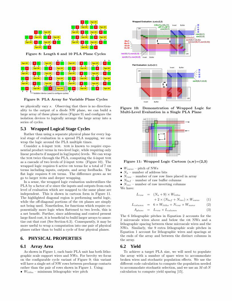
5.3 Wrapped Logical Stage CyclesRather than using a separate physical plane for every log-
ical stage of evaluation in a spread PLA mapping, we canwrap the logic around the PLA multiple times.
Consider a 4-input xor. xor is known to require expo-nential product terms in two-level logic, while requiring onlylinear products if mapped in log(inputs) levels. We can wrapthe xor twice through the PLA, computing the 4-input xoras a cascade of two levels of 2-input xors (Figure 10). Thewrapped logic requires 6 active or terms for a total of 7 orterms including inputs, outputs, and array feedbacks. Theflat logic requires 8 or terms. The difference grows as wego to larger xors and deeper wrapping.
In a sense, the wrapped logic evaluation underutilizes thePLA by a factor of w since the inputs and outputs from eachlevel of evaluation which are mapped to the same plane areindependent. This is shown in cartoon form in Figure 11.The highlighted diagonal region is performing useful logic,while the off-diagonal portions of the or planes are simplynot being used. Nonetheless, for functions which require ex-ponentially more logic when flattened to two levels, this isa net benefit. Further, since addressing and control presentlarge fixed cost, it is beneficial to build larger arrays to amor-tize out that cost (See Section 6.3). Consequently, it may bemore useful to wrap a computation into one pair of physicalplanes rather than to build a cycle of four physical planes.
6. PHYSICAL PROPERTIES
6.1 Array AreaAs shown in Figure 1, each basic PLA unit has both litho-
graphic scale support wires and NWs. For brevity we focuson the configurable cycle variant of Figure 9; this variantwill have a single set of NW rows between precharge contactsrather than the pair of rows shown in Figure 1. Using:• Wlitho – minimum lithographic wire pitch
Invert Buffer
Invert Buffer
OR
/i0+i1i0+/i1/i2+i3i2+/i3
xor(i2,i3)
/xor(i0,i1)+xor(i2,i3)
xor(i0,i1)+/xor(i2,i3)
i0i1i2i3
OR
OR
OR
Invert Buffer
BufferInvert
i0i1i2i3
xor4(i0,i1,i2,i3)
xor4(i0,i1,i2,i3)= xor(xor(i0,i1),xor(i2,i3))
xor(i0,i1)
Wrapped Evaluation: (s,w)=(2,2)
Flat Evaluation: (s,2)=(2,1)
/(/i0+i1)+/(i0+/i1) =i0*/i1+/i0*i1 =xor(i0,i1)
Figure 10: Demonstration of Wrapped Logic forMulti-Level Evaluation in a Single PLA Plane
OR
OR
Figure 11: Wrapped Logic Cartoon (s,w)=(2,3)
• Wnano – pitch of NWs• Na – number of address bits• Nrow – number of raw row lines placed in array• Nbuf – number of raw buffer columns• Ninv – number of raw inverting columnsWe have:
Lrow = (Na + 9)×Wlitho
+ 2× (Nbuf + Ninv)×Wnano (1)
Lcolumn = 6×Wlitho + Nrow ×Wnano (2)
Aplane = Lrow × Lcolumn (3)
The 6 lithographic pitches in Equation 2 accounts for the2 microscale wires above and below the or NWs and alithographic spacing between these microscale wires and theNWs. Similarly, the 9 extra lithographic scale pitches inEquation 1 account for lithographic wires and spacings atthe ends of the array and between the distinct columns inthe array.
6.2 YieldTo achieve a target PLA size, we will need to populate
the array with a number of spare wires to accommodatebroken wires and stochastic population effects. We use thedifferent code calculation to compute the population neededto accommodate stochastic selection, and we use an M -of-Ncalculation to compute yield sparing [15].

400000
500000
600000
700000
800000
900000
1e+006
0 20 40 60 80 100 120 140 160 180 200
Are
a pe
r OR
term
(sq.
nm
.)
Net OR terms
Area vs. OR terms
Share=1 Share=2 Share=3
Wlitho = 210nm; Wnano=10nm; Woverlap=1nm; 50%binate, 25% invert, 25% buffer; 96% plane yield rate
Figure 12: Area per or Term vs. Number of Lines
The whole yield process is best illustrated with an exam-ple. To yield an array with 60 or terms where 30 of its plane-to-plane connections are binate (both inverting and non-inverting), 15 inverting only, and 15 buffered only, we pop-ulate the array with Nrow = 133 and Ninv = Nbuf = 173.With a wire and address alignment yield of 80%, our 133row wires yield us 94 unbroken row wires over 99% of thetime. The 80% yield is calculated based on the length of thewire and the probability of a bad address alignment [15].We use Na = 14 address bits which give us 3432 distinct7-hot codes. Making 94 selections from 3432 codes givesus at least 90 uniquely coded row wires over 99% of thetime. In the restoration stage, wires may be broken (wireyield 86% based on height with 133 row wires), wires maybe uncontrollable because the control region overlaps multi-ple row wires (90% are controllable assuming Woverlap=1nmand Wnano = 10nm [15]), or wires may have their controlregions aligned with unusable row wires (68%=90/133). To-gether, this means the yield rate of a restoring wire is 53%.Consequently, our 173 inverting or buffering inputs provideus with 75 good wires 99% of the time. Selecting 75 wiresfrom the 90 good inputs, we expect 45 or more of them tobe unique 99% of the time. With 45 useful buffering andinverting lines, we can use 30 of each for the binate inputsand the remaining 15 of each for the buffered only or in-verted only inputs. At four steps in this process we said wewould get a number of good or distinct wires 99% of thetime. That means we yield this complete assembly 96% ofthe time (0.994 > 0.96). In practice, we can run the calcu-lations described above in reverse in order to determine theNrow, Ninv, Nbuf required to achieve a target array shapeand to determine the best number of address bits (Na) ortotal row wires (here we used 90 instead of the 60 required)to minimize area.
6.3 Net AreaContinuing the example, with Wlitho = 210nm (90nm pro-
cess [1]) and Wnano = 10nm, the plane will be 11.7µm wideand 2.6µm tall. 4.8µm of the width is in lithographic scalewires, as is 1.3µm of the height. Of the 133 NW rows, only 60will be used for net logic. Of the 692 = 173×4 NW columns,only 180 = 45× 4 provide useful restoration. Clearly, mostof the area of the array is going into lithographic and yieldoverhead. The total area is 11.7µm × 2.6µm ≈ 3× 10⁷nm2;the plane supports 60 or terms, making each or term about500,000nm2.
Figure 12 plots area per or-term versus number of termssupported for a number of array sizes. In each case, we cal-
half or-term Address or-terms forpitch Wlitho area (nm2) Share min. array
90nm 210nm 470,000 2 4065nm 150nm 330,000 2 2045nm 105nm 240,000 2 2022nm 50nm 140,000 2 20
Wnano = 10nm; Woverlap=1nm; 50% binate, 25% in-vert, 25% buffer; 96% plane yield rate
Table 2: Achievable or-Term Area as a Function ofSupporting Lithography
culate appropriate sparing as illustrated in the previous sec-tion then calculate the area of that plane and divide by thenumber of supported or terms to get an area per or term.The three curves represent different levels of row addresssharing. Here we see there is a definite minimum or-termarea around 60 or-term arrays when we do not share the ad-dress and around 40 when we share an address unit acrosstwo arrays. The decreasing area per or-term from 10 to 40or 60 arises from amortizing out the fixed overhead for themicroscale address and control wires. The increasing areaafter the minimum comes from decreasing yield probabilityfor longer NWs and the increased number of restoring wiresneeded to support the outputs.
The lithographic overhead wires have a big effect on den-sity both from the area they consume and because the NWsmust span across them in order to yield. If we use smallerlithography for the programming scaffolding, the minimumachievable area will decrease further as shown in Table 2.
The prediction for 4-transistor gate area at the 22nm nodeis 300,000-500,000nm2 [1]. A 4-LUT logic block in modestsize arrays runs around 500,000 to 1,000,000λ2 [11]; withλ ≈ 11nm for the 22nm node, this means a 4-LUT logicblock will be 50–120,000,000nm2. We note the areas of the22nm 4-LUT and the 4-transistor gate for calibration only.Section 8 quantifies typical, mapped logic densities.
6.4 TimingThe time for a single plane evaluation (See Figure 6) is:
Tplane = Tprecharge + Tno + Teval + Tab (4)
Precharge just needs to discharge row and column capaci-tances through a contact (resistance Rc) and an “on” field-effect NW junction (resistance Ron):
Cwire = max (Crowwire, Ccolwire) (5)
Tprecharge = (Rc + Ron) Cwire (6)
Evaluation in the precharge scheme, charges a number ofrows through “on” diode junctions (resistance Rmem−on):
Teval = (Rc + 2Ron) (Ccolwire + f × Crowwire)
+ Rmem−on × Crowwire (7)
f here is the fanout—the number of rows which use the re-stored term as input. For the static scheme, we need to makethe static pullup resistance weak (See Figure 2, Section 3.2)compared to the pulldown resistance through the diode andthe contact:
Rpu ≈ 10 (Rc + 2Ron + Rmem−on) (8)
It has a similar evaluation equation which is roughly an order
0
5e-009
1e-008
1.5e-008
2e-008
0 10 20 30 40 50 60 70 80 90
Del
ay (s
econ
ds)
Fanout
Delay vs. Fanout
static Share=2static Share=1
precharge Share=2precharge Share=1
60-or-term array; Wlitho = 210nm; Wnano=10nm;Woverlap=1nm; Rc = 100KΩ, Rmem−on = 100KΩ
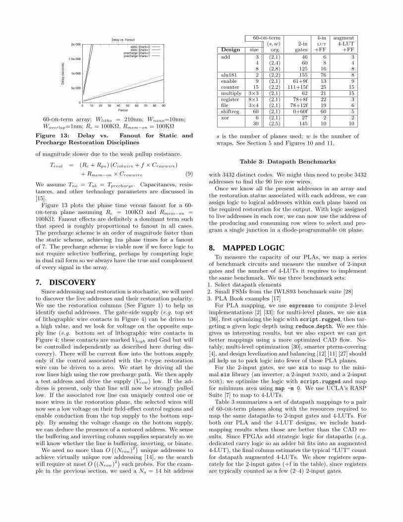
Figure 13: Delay vs. Fanout for Static andPrecharge Restoration Disciplines
of magnitude slower due to the weak pullup resistance.
Teval = (Rc + Rpu) (Ccolwire + f × Crowwire)
+ Rmem−on × Crowwire (9)
We assume Tno = Tab = Tprecharge. Capacitances, resis-tances, and other technology parameters are discussed in[15].
Figure 13 plots the phase time versus fanout for a 60-or-term plane assuming Rc = 100KΩ and Rmem−on =100KΩ. Fanout effects are definitely a dominant term suchthat speed is roughly proportional to fanout in all cases.The precharge scheme is an order of magnitude faster thanthe static scheme, achieving 1ns phase times for a fanoutof 7. The precharge scheme is viable now if we force logic tonot require selective buffering, perhaps by computing logicin dual rail form so we always have the true and complementof every signal in the array.
7. DISCOVERYSince addressing and restoration is stochastic, we will need
to discover the live addresses and their restoration polarity.We use the restoration columns (See Figure 1) to help usidentify useful addresses. The gate-side supply (e.g. top setof lithographic wire contacts in Figure 4) can be driven toa high value, and we look for voltage on the opposite sup-ply line (e.g. bottom set of lithographic wire contacts inFigure 4; these contacts are marked Vhigh and Gnd but willbe controlled independently as described here during dis-covery). There will be current flow into the bottom supplyonly if the control associated with the p-type restorationwire can be driven to a zero. We start by driving all therow lines high using the row precharge path. We then applya test address and drive the supply (Vrow) low. If the ad-dress is present, only that line will now be strongly pulledlow. If the associated row line can uniquely control one ormore wires in the restoration plane, the selected wires willnow see a low voltage on their field-effect control regions andenable conduction from the top supply to the bottom sup-ply. By sensing the voltage change on the bottom supply,we can deduce the presence of a restored address. We sensethe buffering and inverting column supplies separately so wewill know whether the line is buffering, inverting, or binate.
We need no more than O((Nrow)2
)unique addresses to
achieve virtually unique row addressing [14], so the searchwill require at most O
((Nrow)2
)such probes. For the exam-
ple in the previous section, we used a Na = 14 bit address
60-or-term 4-in augment(s, w) 2-in LUT 4-LUT
Design size org. gates +FF +FF
add 3 (2,1) 46 6 34 (2,4) 60 8 48 (2,8) 125 16 8
alu181 2 (2,2) 155 76 8enable 9 (2,1) 61+9f 13 9counter 15 (2,2) 111+15f 25 15multiply 3×3 (2,1) 62 21 15register 8×1 (2,1) 78+8f 22 3file 3×4 (2,1) 78+12f 19 6shiftreg 60 (2,1) 0+60f 60 5xor 6 (2,1) 27 2 2
30 (2,5) 145 10 10
s is the number of planes used; w is the number ofwraps. See Section 5 and Figures 10 and 11.
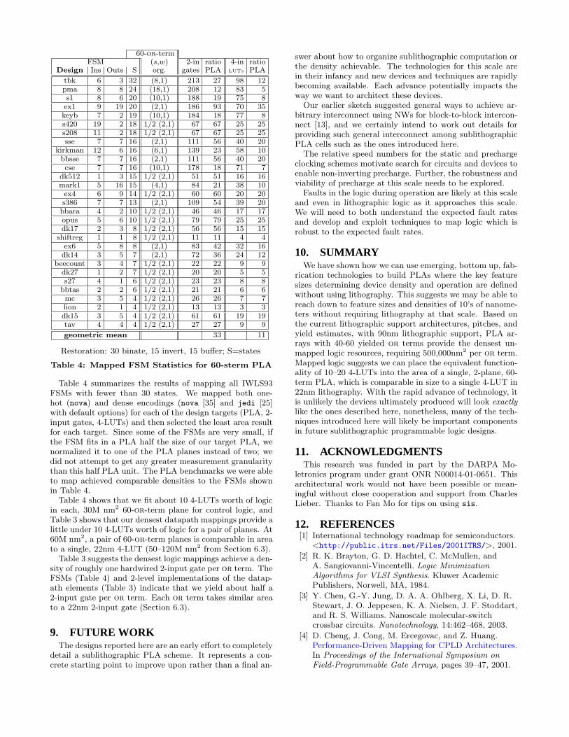
Table 3: Datapath Benchmarks
with 3432 distinct codes. We might thus need to probe 3432addresses to find the 90 live row wires.
Once we know all the present addresses in an array andthe restoration status associated with each address, we canassign logic to logical addresses within each plane based onthe required restoration for the output. With logic assignedto live addresses in each row, we can now use the address ofthe producing and consuming row wires to select and pro-gram a single junction in a diode-programmable or plane.
8. MAPPED LOGICTo measure the capacity of our PLAs, we map a series
of benchmark circuits and measure the number of 2-inputgates and the number of 4-LUTs it requires to implementthe same benchmark. We use three benchmark sets:1. Select datapath elements2. Small FSMs from the IWLS93 benchmark suite [28]3. PLA Book examples [17]
For PLA mapping, we use espresso to compute 2-levelimplementations [2] [33]; for multi-level planes, we use sis
[36], first optimizing the logic with script.rugged, then tar-geting a given logic depth using reduce depth. We see thisgives us interesting results, but we also expect we can getbetter mappings using a more optimized CAD flow. No-tably, multi-level optimization [30], smarter pterm-covering[4], and design levelization and balancing [12] [11] [27] shouldall help us to pack logic into fewer of these PLA planes.
For the 2-input gates, we use sis to map to the mini-mal sis library (an inverter, a 2-input nand, and a 2-inputnor); we optimize the logic with script.rugged and mapfor minimum area using map -m 0. We use UCLA’s RASPSuite [7] to map to 4-LUTs.
Table 3 summarizes a set of datapath mappings to a pairof 60-or-term planes along with the resources required tomap the same datapaths to 2-input gates and 4-LUTs. Forboth our PLA and the 4-LUT designs, we include hand-mapping results when those are better than the CAD re-sults. Since FPGAs add strategic logic for datapaths (e.g.dedicated carry logic so an adder bit fits into an augmented4-LUT), the final column estimates the typical “LUT” countfor datapath augmented 4-LUTs. We show registers sepa-rately for the 2-input gates (+f in the table), since registersare typically counted as a few (2–4) 2-input gates.
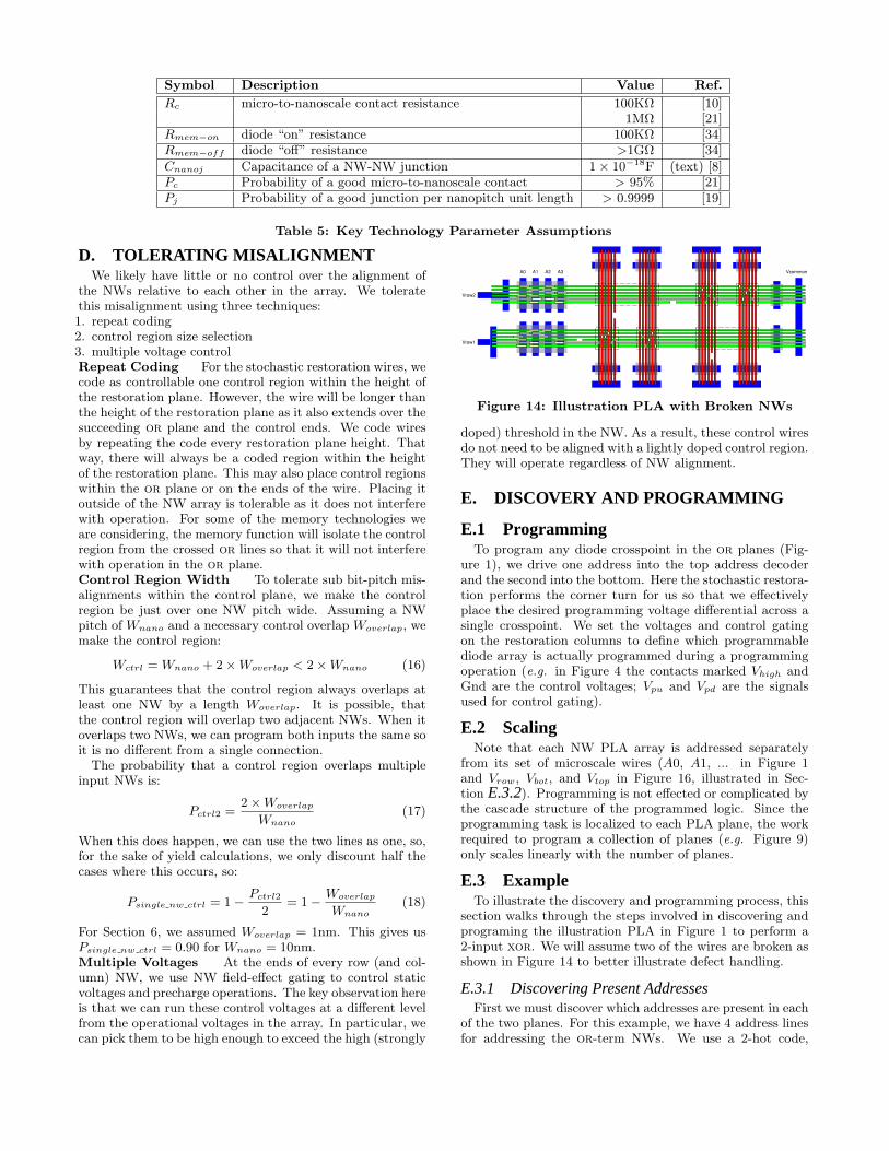
60-or-termFSM (s,w) 2-in ratio 4-in ratio
Design Ins Outs S org. gates PLA LUTs PLA
tbk 6 3 32 (8,1) 213 27 98 12pma 8 8 24 (18,1) 208 12 83 5s1 8 6 20 (10,1) 188 19 75 8ex1 9 19 20 (2,1) 186 93 70 35keyb 7 2 19 (10,1) 184 18 77 8s420 19 2 18 1/2 (2,1) 67 67 25 25s208 11 2 18 1/2 (2,1) 67 67 25 25sse 7 7 16 (2,1) 111 56 40 20
kirkman 12 6 16 (6,1) 139 23 58 10bbsse 7 7 16 (2,1) 111 56 40 20cse 7 7 16 (10,1) 178 18 71 7
dk512 1 3 15 1/2 (2,1) 51 51 16 16mark1 5 16 15 (4,1) 84 21 38 10ex4 6 9 14 1/2 (2,1) 60 60 20 20s386 7 7 13 (2,1) 109 54 39 20bbara 4 2 10 1/2 (2,1) 46 46 17 17opus 5 6 10 1/2 (2,1) 79 79 25 25dk17 2 3 8 1/2 (2,1) 56 56 15 15
shiftreg 1 1 8 1/2 (2,1) 11 11 4 4ex6 5 8 8 (2,1) 83 42 32 16dk14 3 5 7 (2,1) 72 36 24 12
beecount 3 4 7 1/2 (2,1) 22 22 9 9dk27 1 2 7 1/2 (2,1) 20 20 5 5s27 4 1 6 1/2 (2,1) 23 23 8 8
bbtas 2 2 6 1/2 (2,1) 21 21 6 6mc 3 5 4 1/2 (2,1) 26 26 7 7lion 2 1 4 1/2 (2,1) 13 13 3 3dk15 3 5 4 1/2 (2,1) 61 61 19 19tav 4 4 4 1/2 (2,1) 27 27 9 9
geometric mean 33 11
Restoration: 30 binate, 15 invert, 15 buffer; S=states
Table 4: Mapped FSM Statistics for 60-sterm PLA
Table 4 summarizes the results of mapping all IWLS93FSMs with fewer than 30 states. We mapped both one-hot (nova) and dense encodings (nova [35] and jedi [25]with default options) for each of the design targets (PLA, 2-input gates, 4-LUTs) and then selected the least area resultfor each target. Since some of the FSMs are very small, ifthe FSM fits in a PLA half the size of our target PLA, wenormalized it to one of the PLA planes instead of two; wedid not attempt to get any greater measurement granularitythan this half PLA unit. The PLA benchmarks we were ableto map achieved comparable densities to the FSMs shownin Table 4.
Table 4 shows that we fit about 10 4-LUTs worth of logicin each, 30M nm2 60-or-term plane for control logic, andTable 3 shows that our densest datapath mappings provide alittle under 10 4-LUTs worth of logic for a pair of planes. At60M nm2, a pair of 60-or-term planes is comparable in areato a single, 22nm 4-LUT (50–120M nm2 from Section 6.3).
Table 3 suggests the densest logic mappings achieve a den-sity of roughly one hardwired 2-input gate per or term. TheFSMs (Table 4) and 2-level implementations of the datap-ath elements (Table 3) indicate that we yield about half a2-input gate per or term. Each or term takes similar areato a 22nm 2-input gate (Section 6.3).
9. FUTURE WORKThe designs reported here are an early effort to completely
detail a sublithographic PLA scheme. It represents a con-crete starting point to improve upon rather than a final an-
swer about how to organize sublithographic computation orthe density achievable. The technologies for this scale arein their infancy and new devices and techniques are rapidlybecoming available. Each advance potentially impacts theway we want to architect these devices.
Our earlier sketch suggested general ways to achieve ar-bitrary interconnect using NWs for block-to-block intercon-nect [13], and we certainly intend to work out details forproviding such general interconnect among sublithographicPLA cells such as the ones introduced here.
The relative speed numbers for the static and prechargeclocking schemes motivate search for circuits and devices toenable non-inverting precharge. Further, the robustness andviability of precharge at this scale needs to be explored.
Faults in the logic during operation are likely at this scaleand even in lithographic logic as it approaches this scale.We will need to both understand the expected fault ratesand develop and exploit techniques to map logic which isrobust to the expected fault rates.
10. SUMMARYWe have shown how we can use emerging, bottom up, fab-
rication technologies to build PLAs where the key featuresizes determining device density and operation are definedwithout using lithography. This suggests we may be able toreach down to feature sizes and densities of 10’s of nanome-ters without requiring lithography at that scale. Based onthe current lithographic support architectures, pitches, andyield estimates, with 90nm lithographic support, PLA ar-rays with 40-60 yielded or terms provide the densest un-mapped logic resources, requiring 500,000nm2 per or term.Mapped logic suggests we can place the equivalent function-ality of 10–20 4-LUTs into the area of a single, 2-plane, 60-term PLA, which is comparable in size to a single 4-LUT in22nm lithography. With the rapid advance of technology, itis unlikely the devices ultimately produced will look exactlylike the ones described here, nonetheless, many of the tech-niques introduced here will likely be important componentsin future sublithographic programmable logic designs.
11. ACKNOWLEDGMENTSThis research was funded in part by the DARPA Mo-
letronics program under grant ONR N00014-01-0651. Thisarchitectural work would not have been possible or mean-ingful without close cooperation and support from CharlesLieber. Thanks to Fan Mo for tips on using sis.
12. REFERENCES[1] International technology roadmap for semiconductors.
<http://public.itrs.net/Files/2001ITRS/>, 2001.
[2] R. K. Brayton, G. D. Hachtel, C. McMullen, andA. Sangiovanni-Vincentelli. Logic MinimizationAlgorithms for VLSI Synthesis. Kluwer AcademicPublishers, Norwell, MA, 1984.
[3] Y. Chen, G.-Y. Jung, D. A. A. Ohlberg, X. Li, D. R.Stewart, J. O. Jeppesen, K. A. Nielsen, J. F. Stoddart,and R. S. Williams. Nanoscale molecular-switchcrossbar circuits. Nanotechnology, 14:462–468, 2003.
[4] D. Cheng, J. Cong, M. Ercegovac, and Z. Huang.Performance-Driven Mapping for CPLD Architectures.In Proceedings of the International Symposium onField-Programmable Gate Arrays, pages 39–47, 2001.

[5] C. Collier, G. Mattersteig, E. Wong, Y. Luo,K. Beverly, J. Sampaio, F. Raymo, J. Stoddart, andJ. Heath. A [2]Catenane-Based Solid StateReconfigurable Switch. Science, 289:1172–1175, 2000.
[6] C. P. Collier, E. W. Wong, M. Belohradsky, F. M.Raymo, J. F. Stoddard, P. J. Kuekes, R. S. Williams,and J. R. Heath. Electronically configurablemolecular-based logic gates. Science, 285:391–394,1999.
[7] J. Cong, E. Ding, Y.-Y. Hwang, J. Peck, C. Wu, andS. Xu. RASP SYN release B 1.1: LUT-Based FPGATechnology Mapping Package. <http://cadlab.cs.
ucla.edu/~xfpga/software/raspsyn.htm>, 1999.
[8] Y. Cui, X. Duan, J. Hu, and C. M. Lieber. Dopingand electrical transport in silicon nanowires. Journalof Physical Chemistry B, 104(22):5213–5216, June 82000.
[9] Y. Cui, L. J. Lauhon, M. S. Gudiksen, J. Wang, andC. M. Lieber. Diameter-controlled synthesis of singlecrystal silicon nanowires. Applied Physics Letters,78(15):2214–2216, 2001.
[10] Y. Cui, Z. Zhong, D. Wang, W. U. Wang, and C. M.Lieber. High Performance Silicon Nanowire FieldEffect Transistors. Nanoletters, 3(2):149–152, 2003.
[11] A. DeHon. Reconfigurable Architectures forGeneral-Purpose Computing. AI Technical Report1586, MIT Artificial Intelligence Laboratory, 545Technology Sq., Cambridge, MA 02139, October 1996.
[12] A. DeHon. DPGA Utilization and Application. InProceedings of the International Symposium onField-Programmable Gate Arrays, February 1996.
[13] A. DeHon. Array-Based Architecture for FET-based,Nanoscale Electronics. IEEE Transactions onNanotechnology, 2(1):23–32, March 2003.
[14] A. DeHon, P. Lincoln, and J. Savage. StochasticAssembly of Sublithographic Nanoscale Interfaces.IEEE Transactions on Nanotechnology, 2(3):165–174,2003.
[15] A. DeHon and M. J. Wilson. Nanowire-BasedSublithographic Programmable Logic Arrays[Extended Version with Detail Appendix]. URL:<http://www.cs.caltech.edu/research/ic/
abstracts/nanopla_fpga2004.html>, January 2004.
[16] S. C. Goldstein and M. Budiu. NanoFabrics: SpatialComputing Using Molecular Electronics. InProceedings of the International Symposium onComputer Architecture, pages 178–189, June 2001.
[17] U. C. Group. Espresso examples. Online<ftp://ic.eecs.berkeley.edu/pub/Espresso/
espresso-book-examples.tar.gz>, June 1993.
[18] M. S. Gudiksen, L. J. Lauhon, J. Wang, D. C. Smith,and C. M. Lieber. Growth of nanowire superlatticestructures for nanoscale photonics and electronics.Nature, 415:617–620, February 7 2002.
[19] M. S. Gudiksen, J. Wang, and C. M. Lieber. Syntheticcontrol of the diameter and length of semiconductornanowires. Journal of Physical Chemistry B,105:4062–4064, 2001.
[20] J. R. Heath, P. J. Kuekes, G. S. Snider, and R. S.Williams. A defect-tolerant computer architecture:Opportunities for nanotechnology. Science,280:1716–1721, June 12 1998.
[21] Y. Huang, X. Duan, Y. Cui, L. Lauhon, K. Kim, andC. M. Lieber. Logic gates and computation fromassembled nanowire building blocks. Science,294:1313–1317, 2001.
[22] Y. Huang, X. Duan, Q. Wei, and C. M. Lieber.Directed assembley of one-dimensional nanostructuresinto functional networks. Science, 291:630–633,January 26 2001.
[23] J. Kouloheris and A. E. Gamal. Pla-based fpga areaversus cell granularity. In Proceedings of the CustomIntegrated Circuits Conference, pages 4.3.1–4. IEEE,May 1992.
[24] C. M. Lieber. Nanowire contact resistance. PersonalCommunications, July 2003.
[25] B. Lin and R. Newton. Synthesis of multiple-levellogic from symbolic high-level description languages.In Proceedings of the IFIP International Conferenceon VLSI, pages 187–196, 1989.
[26] M. S. G. Lincoln J. Lauhon, D. Wang, and C. M.Lieber. Epitaxial core-shell and core-multi-shellnanowire heterostructures. Nature, 420:57–61, 2002.
[27] H. Liu and D. F. Wong. Network flow basedpartitioning for time-multiplexed fpgas. In Proceedingsof the IEEE/ACM International Conference onComputer-Adided Design, pages 497–504, 1998.
[28] K. McElvain. LGSynth93 Benchmark Set: Version 4.0.Online <http://www.cbl.ncsu.edu/pub/Benchmark_
dirs/LGSynth93/doc/iwls93.ps>, May 1993.
[29] P. L. McEuen, M. Fuhrer, and H. Park. Single-walledcarbon nanotubes electronics. IEEE Transactions onNanotechnology, 1(1):75–85, March 2002.
[30] F. Mo and R. K. Brayton. Whirlpool PLAs: ARegular Logic Structure and Their Synthesis. InProceedings of the International Conference onComputer-Aided Design, pages 543–550, November2002.
[31] A. M. Morales and C. M. Lieber. A laser ablationmethod for synthesis of crystalline semiconductornanowires. Science, 279:208–211, 1998.
[32] M. T. Niemier, A. F. Rodrigues, and P. M. Kogge. APotentially Implementable FPGA for Quantum DotCellular Automata. In Proceedings of the FirstWorkshop on Non-Silicon Computation (NSC-1),Boston, MA, February 2002.
[33] R. Rudell and A. Sangiovanni-Vincentelli.Multiple-valued minimization for pla optimization.IEEE Transactions on Computer-Aided Design ofIntegrated Circuits, 6(5):727–751, September 1987.
[34] T. Rueckes, K. Kim, E. Joselevich, G. Y. Tseng, C.-L.Cheung, and C. M. Lieber. Carbon nanotube basednonvolatile random access memory for molecularcomputing. Science, 289:94–97, 2000.
[35] T. V. A. Sangiovanni-Vincentelli. NOVA: stateassignment of finite state machines for optimaltwo-level logic implementations. In Proceedings of theACM/IEEE Design Automation Conference, pages327–332, 1989.
[36] E. M. Sentovich, K. J. Singh, L. Lavagno, C. Moon,R. Murgai, A. Saldanha, H. Savoj, P. R. Stephan,R. K. Brayton, and A. Sangiovanni-Vincentelli. Sis: Asystem for sequential circuit synthesis. UCB/ERLM92/41, University of California, Berkeley, May 1992.

[37] J. M. Tour. Molecular Electronics: CommercialInsights, Chemistry, Devices, Architecture andProgramming. World Scientific Publishing Company,New Jersey, 2003.
[38] D. Whang, S. Jin, and C. M. Lieber. Nanolithographyusing hierarchically assembled nanowire masks.Nanoletters, 3(7):951–954, July 9 2003.
[39] D. Whang, S. Jin, Y. Wu, and C. M. Lieber.Large-scale hierarchical organization of nanowirearrays for integrated nanosystems. Nanoletters,3(9):1255–1259, September 2003.
APPENDIX
A. TECHNOLOGY ASSUMPTIONSTable 5 summarizes some of the key technology parame-
ters assumed for this analysis along with references.Resistance For nanotubes, the fundamental limit oncontact resistance is 6.5KΩ and it appears to be possibleto approach this limit [29]; consequently, it should be pos-sible to decrease contact resistance with further technologymastery.Capacitance From [8] the capacitance of a NW junctionis:
Cjunc ≈ 2πεSiO2
L
ln(2h/r)
Where r is the NW radius, h is the distance between con-ductors, and l is the length of the overlap. For the NWjunctions, we assume: r = 1nm, h = 1nm, L = 2r.
Cnanoj ≈ 2π(3.4× 10⁻¹¹F/m)
(2nm
ln(2)
)≈ 6× 10⁻¹⁹F (10)
We use Cnanoj = 10−18F as a rough approximation here.For the NW runs over the microwires, L = Wlitho/2 as-suming half the pitch is in the wire and half in the spacingbetween wires. Here height is oxide thickness between theaddress lines and the nanoscale core memory wires which islikely to be 5–10nm (assume h = 5nm).
Cmicroj ≈ 2π(3.4× 10⁻¹¹F/m)
(Wlitho/2
ln(2× 5/1)
)(11)
Assuming the dominant capacitance is junction capacitancebetween crossed NW junctions and NW over microwire junc-tions, we can calculate the nanoscale junction capacitance(Cnanoj) and nano-micro junction capacitance (Cmicroj) andestimate the total row and column wire capacitances:
Ccolwire = Nrow × Cnanoj + 2× Cmicroj
Crowwire = Ncolumn × Cnanoj + (Na + 1)× Cmicroj
This assumes we have to charge up all the capacitance as-sociated with the address lines. We can isolate the addresslines during operation, so that we only pay for two microwirejunctions in the row case as well.Wire Yield For an N junction long NW to yield, it mustmake good contact on both ends and contain no junctionfailures along its length:
Pgoodwire = (Pc)2 × (Pj)
N (12)
[19] reports reliable growth of SiNWs which are over 9µmlong (i.e. no breaks over a distance equivalent to 900 10nm
junction lengths). More recently, Lieber is seeing over 90%yield of NWs up to 20µm long [24], which would correspondto Pj > 0.99995.
B. STOCHASTIC SELECTIONLet C be the number of codes in our code space, N be the
number of selection we make (number of wires chosen), andu be the number of distinct codes appearing in our selection.We can calculate the probability distribution for the num-ber of different codes, u, in an array, using the recurrencerelation:
Pdifferent(C, N, u) =(C − (u− 1)
C
)× Pdifferent(C, N − 1, u− 1)
+( u
C
)× Pdifferent(C, N − 1, u) (13)
The base cases are:• Pdifferent(C, 1, 1) = 1 (if we pick one thing, we get one
different thing)• Pdifferent(C, 1, u 6= 1) = 0 (if we pick one, we will get
exactly one different thing)• Pdifferent(C, 0, 0) = 1 (if we pick nothing, we get nothing)• Pdifferent(C, 0, u > 0) = 0 (if we pick nothing, we get
nothing)• Pdifferent(C, N, u < 0) = 0 (we cannot have less than
nothing)This recurrence counts each code once even if it appearsmultiple times, which is what we want if we allow duplicatecodes in the addressing or duplicate restoration.
Since we are generally interested in achieving at least acertain number of codes, we are interested in the cumulativedistribution function (CDF) for the probability that we haveat least a certain number of codes. We calculate this:
Pat least (C, M, u) =
M∑i=u
Pdifferent (C, M, i) (14)
Table 1 is generated with C = Ninputs and M = Nrestore;we set a target for Pat least, 99% in this case, and find thelargest u for which Pat least exceeds the target.
C. N-CHOOSE-M CALCULATIONA common calculation used for defect tolerant design is
the probability that we yield at least M elements form a fullset of N . Assuming each element yields independently withprobability, P , the probability that we will yield M ≤ Nthings is:
PMofN =∑
M≤i≤N
((N
i
)P i (1− P )N−i
)(15)
or term yield is a common example where this calculationis relevant in our nanoscale PLA. Here, N is the number ofNWs we assemble into the array, M is the number of NWswe yield, and P is the probability that the NW yields (e.g.is not broken or shorted; see Equation 12). PMofN in theequation above, tells us the probability that we will yieldthe specified M NWs. In design, we typically pick a targetvalue for PMofN , such as 0.99, then look for the largest M forwhich the calculated PMofN exceeds the target probability.
Symbol Description Value Ref.
Rc micro-to-nanoscale contact resistance 100KΩ [10]1MΩ [21]
Rmem−on diode “on” resistance 100KΩ [34]Rmem−off diode “off” resistance >1GΩ [34]Cnanoj Capacitance of a NW-NW junction 1× 10⁻¹⁸F (text) [8]Pc Probability of a good micro-to-nanoscale contact > 95% [21]Pj Probability of a good junction per nanopitch unit length > 0.9999 [19]
Table 5: Key Technology Parameter Assumptions
D. TOLERATING MISALIGNMENTWe likely have little or no control over the alignment of
the NWs relative to each other in the array. We toleratethis misalignment using three techniques:1. repeat coding2. control region size selection3. multiple voltage controlRepeat Coding For the stochastic restoration wires, wecode as controllable one control region within the height ofthe restoration plane. However, the wire will be longer thanthe height of the restoration plane as it also extends over thesucceeding or plane and the control ends. We code wiresby repeating the code every restoration plane height. Thatway, there will always be a coded region within the heightof the restoration plane. This may also place control regionswithin the or plane or on the ends of the wire. Placing itoutside of the NW array is tolerable as it does not interferewith operation. For some of the memory technologies weare considering, the memory function will isolate the controlregion from the crossed or lines so that it will not interferewith operation in the or plane.Control Region Width To tolerate sub bit-pitch mis-alignments within the control plane, we make the controlregion be just over one NW pitch wide. Assuming a NWpitch of Wnano and a necessary control overlap Woverlap, wemake the control region:
Wctrl = Wnano + 2×Woverlap < 2×Wnano (16)
This guarantees that the control region always overlaps atleast one NW by a length Woverlap. It is possible, thatthe control region will overlap two adjacent NWs. When itoverlaps two NWs, we can program both inputs the same soit is no different from a single connection.
The probability that a control region overlaps multipleinput NWs is:
Pctrl2 =2×Woverlap
Wnano(17)
When this does happen, we can use the two lines as one, so,for the sake of yield calculations, we only discount half thecases where this occurs, so:
Psingle nw ctrl = 1− Pctrl2
2= 1− Woverlap
Wnano(18)
For Section 6, we assumed Woverlap = 1nm. This gives usPsingle nw ctrl = 0.90 for Wnano = 10nm.Multiple Voltages At the ends of every row (and col-umn) NW, we use NW field-effect gating to control staticvoltages and precharge operations. The key observation hereis that we can run these control voltages at a different levelfrom the operational voltages in the array. In particular, wecan pick them to be high enough to exceed the high (strongly
Vrow1
Vrow2
A0 A1 A2 A3 Vcommon
Figure 14: Illustration PLA with Broken NWs
doped) threshold in the NW. As a result, these control wiresdo not need to be aligned with a lightly doped control region.They will operate regardless of NW alignment.
E. DISCOVERY AND PROGRAMMING
E.1 ProgrammingTo program any diode crosspoint in the or planes (Fig-
ure 1), we drive one address into the top address decoderand the second into the bottom. Here the stochastic restora-tion performs the corner turn for us so that we effectivelyplace the desired programming voltage differential across asingle crosspoint. We set the voltages and control gatingon the restoration columns to define which programmablediode array is actually programmed during a programmingoperation (e.g. in Figure 4 the contacts marked Vhigh andGnd are the control voltages; Vpu and Vpd are the signalsused for control gating).
E.2 ScalingNote that each NW PLA array is addressed separately
from its set of microscale wires (A0, A1, ... in Figure 1and Vrow, Vbot, and Vtop in Figure 16, illustrated in Sec-tion E.3.2). Programming is not effected or complicated bythe cascade structure of the programmed logic. Since theprogramming task is localized to each PLA plane, the workrequired to program a collection of planes (e.g. Figure 9)only scales linearly with the number of planes.
E.3 ExampleTo illustrate the discovery and programming process, this
section walks through the steps involved in discovering andprograming the illustration PLA in Figure 1 to perform a2-input xor. We will assume two of the wires are broken asshown in Figure 14 to better illustrate defect handling.
E.3.1 Discovering Present AddressesFirst we must discover which addresses are present in each
of the two planes. For this example, we have 4 address linesfor addressing the or-term NWs. We use a 2-hot code,
meaning there are(42
)= 6 possible addresses for the or
terms in each plane (1100, 1010, 0110, 1001, 0101, 0011).So, for each plane, we need to test each of the 6 addresses.
To test for an address’s presence, we:1. Drive the right end common supply (Vcommon in Fig-
ure 14) to ground, then release it.2. Drive the address lines (A0, A1, ... ) to the test address.3. Drive the common row line (i.e. Vrow1 or Vrow2 in Fig-
ure 14) to high.4. Observe the voltage on the common line (Vcommon).The common line will be raised to high only if the test ad-dress is present allowing a complete path between Vrow andVcommon. Figure 15A shows an attempt to read the address1001 on the top plane. Since the 1001 wire is not present,this results in no current path from Vrow2 to Vcommon andVcommon remains low. Figure 15B shows an attempt to readthe address 1100 on the top plane. Since the 1100 wire ispresent and unbroken, this does succeed in raising the volt-age on Vcommon. In Figure 15C, we see that an attempt toread address 0101 does not raise Vcommon since the wire hasa break in it. After testing all six addresses, we know thatthe present and functional addresses in the top plane are1100, 1010, 0110, and 0011. Similar testing for the bottomplane tells us the present and function addresses there are1100, 1010, 0110, and 0101.
E.3.2 Discovering PolaritiesKnowing which addresses are present, we can determine
which polarities they provide. We drive each good addressto a low voltage, while keeping the other wires high, andobserve if the output is restored. For each address we:1. Set the gate-side supplies on the restoration column (Vtop
in Figure 16) to a low voltage.2. Drive the opposite supplies (Vbot in Figure 16) to a low
voltage and release.3. Use Vcommon and Vrow to precharge alls lines to a high
voltage. Drive the addresses (A0, A1,...) to all ones dur-ing this precharge. Note that we drive high from bothsides; this way even wires with a single break are chargedto a high voltage.
4. Release Vcommon, Vrow and return the addresses to zeros.5. Drive the intended address on the address lines.6. Drive Vrow to a low voltage.7. After the row line has had time to discharge, drive the
gate-side supplies on the appropriate restoration columns(Vtop in Figure 16) to a high voltage.
8. Observe the voltage on the opposite supply (e.g. Vbot)once the restoration line has had a chance to charge.
Remember the restoration wires are p-type NWs. A highvoltage across their lightly-doped control region will depletecarries and prevent conduction, while a low voltage will al-low conduction. In steps 3–6, we guarantee that only theaddressed row is low; all other rows are driven to a highvalue. As a result, we will only see conduction between Vtop
and Vbot in a column if the addressed NW controls some NWin that column.
Figure 16A shows how we test the 1100 wire. As de-scribed above, we drive only the 1100 wire to a low volt-age. The restoration columns for this wire are bracketed byVtop3/Vbot3 and Vtop4/Vbot4, so we drive Vtop3 and Vtop4 tohigh voltages and watch the voltage on Vbot3 and Vbot4. No-tice that the 1100 NW intersects with two control regions inrestoration column 3 and no control regions in restoration
Vrow1
Vrow2
A0 A1 A2 A3 Vcommon
A: 1001 Address (non-present)
Vrow1
Vrow2
A0 A1 A2 A3 Vcommon
B: 1100 Address (present)
Vrow1
Vrow2
A0 A1 A2 A3 Vcommon
C: 0101 Address (defective NW)
Light grey lines are at ground;black lines driven to high voltage.
Figure 15: Testing Functional Address Presence
column 4. Consequently, Vbot3 is pulled high while Vbot4 re-mains low. By convention (See Figures 1 and 4), column 3is our inverting column. This tells us the 1100 or term canonly be used in its inverting sense.
In Figure 16B we show testing of the 1010 wire. The1010 wire controls restoration wires in both columns 3 and4. However, the restoration wire in column 3 is broken.Consequently only the restoration in column 4 is usable.Vbot4 is pulled high, but Vbot3 remains low because of thebroken column 3 wire. We conclude that we can use the1010 or term only in its non-inverting sense.
Figure 16C shows the result of testing the 0110 wire.There are two 0110 wires in the top plane. Consequently,when we address 0110 we affect both of them. Since the twowires have the same address, we will always select them intandem. Both or terms are charged low. It further turnsout that there are multiple wires in both column 3 and col-umn 4 controlled by either of the two 0110 or terms. BothVbot3 and Vbot4 are driven high telling us that we can useboth polarities of the 0110 or-term (i.e. it is binate). Test-ing the 0011 or-term in a similar manner, we learn that itcan only be used in the non-inverted sense.
We can perform similar test for the lower or plane. In thiscase, the outputs of this or plane are restored by columns 1
Vrow1
Vrow2
A0 A1 A2 A3 Vcommon
Vtop1 Vtop2 Vtop3 Vtop4
Vbot1 Vbot2 Vbot3 Vbot4
A: 1100 NW (inverting)
Vrow1
Vrow2
A0 A1 A2 A3 Vcommon
Vtop1 Vtop2 Vtop3 Vtop4
Vbot1 Vbot2 Vbot3 Vbot4
B: 1010 NW (non-inverting)
Vrow1
Vrow2
A0 A1 A2 A3 Vcommon
Vtop1 Vtop2 Vtop3 Vtop4
Vbot1 Vbot2 Vbot3 Vbot4
C: 0110 NW (binate)
Figure 16: Discovering Restoration Polarities
and 2. We drive the high test values into Vbot1 and Vbot2 andobserve the voltages at Vtop1 and Vtop2; the role of top andbottom supplies are reversed compared to the top or planeto match the fact that the position of the restoration arrayand the succeeding or array are reversed. After performingthe test, we learn the that 1100 and 1010 are binate, 0110is non-inverting, and 0101 is inverting.
E.3.3 Programming Diode CrosspointsKnowing which polarities are available from each of the
present addresses, we can program up the intended function.Figure 17 shows our assignment of known, good or terms
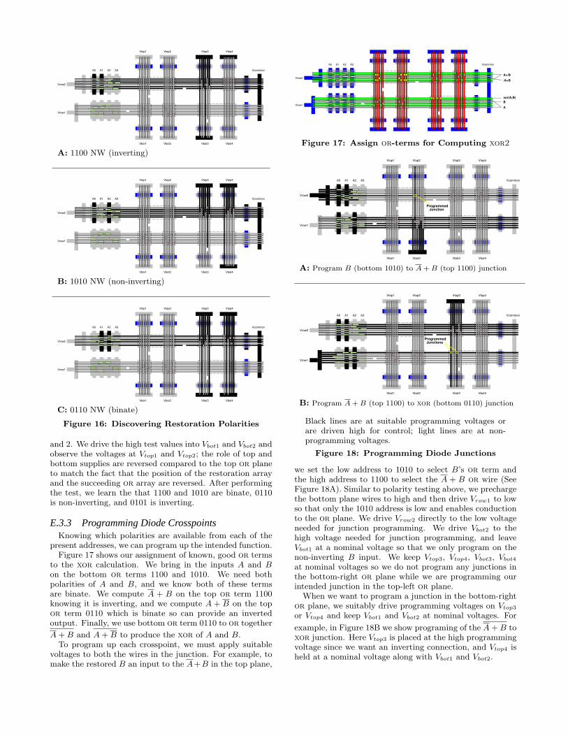
to the xor calculation. We bring in the inputs A and Bon the bottom or terms 1100 and 1010. We need bothpolarities of A and B, and we know both of these termsare binate. We compute A + B on the top or term 1100knowing it is inverting, and we compute A + B on the topor term 0110 which is binate so can provide an invertedoutput. Finally, we use bottom or term 0110 to or together
A + B and A + B to produce the xor of A and B.To program up each crosspoint, we must apply suitable
voltages to both the wires in the junction. For example, tomake the restored B an input to the A+B in the top plane,
Vrow1
Vrow2
A0 A1 A2 A3 Vcommon
A
Bxor(A,B)
/A+B
A+/B
Figure 17: Assign or-terms for Computing xor2
Vrow1
Vrow2
A0 A1 A2 A3 Vcommon
Vtop1 Vtop2 Vtop3 Vtop4
Vbot1 Vbot2 Vbot3 Vbot4
Programmed Junction
A: Program B (bottom 1010) to A + B (top 1100) junction
Vrow1
Vrow2
A0 A1 A2 A3 Vcommon
Vtop1 Vtop2 Vtop3 Vtop4
Vbot1 Vbot2 Vbot3 Vbot4
Programmed Junctions
B: Program A + B (top 1100) to xor (bottom 0110) junction
Black lines are at suitable programming voltages orare driven high for control; light lines are at non-programming voltages.
Figure 18: Programming Diode Junctions
we set the low address to 1010 to select B’s or term andthe high address to 1100 to select the A + B or wire (SeeFigure 18A). Similar to polarity testing above, we prechargethe bottom plane wires to high and then drive Vrow1 to lowso that only the 1010 address is low and enables conductionto the or plane. We drive Vrow2 directly to the low voltageneeded for junction programming. We drive Vbot2 to thehigh voltage needed for junction programming, and leaveVbot1 at a nominal voltage so that we only program on thenon-inverting B input. We keep Vtop3, Vtop4, Vbot3, Vbot4
at nominal voltages so we do not program any junctions inthe bottom-right or plane while we are programming ourintended junction in the top-left or plane.
When we want to program a junction in the bottom-rightor plane, we suitably drive programming voltages on Vtop3
or Vtop4 and keep Vbot1 and Vbot2 at nominal voltages. For
example, in Figure 18B we show programing of the A + B toxor junction. Here Vtop3 is placed at the high programmingvoltage since we want an inverting connection, and Vtop4 isheld at a nominal voltage along with Vbot1 and Vbot2.