
Nanostructured Tungsten Trioxide Thin Films Synthesized for ...
24
DOI: 10.1002/cssc.201402089 Nanostructured Tungsten Trioxide Thin Films Synthesized for Photoelectrocatalytic Water Oxidation: A review Tao Zhu, Meng Nan Chong,* and Eng Seng Chan [a] # 2014 Wiley-VCH Verlag GmbH & Co. KGaA, Weinheim ChemSusChem 2014, 7, 2974 – 2997 2974 CHEMSUSCHEM REVIEWS
Transcript of Nanostructured Tungsten Trioxide Thin Films Synthesized for ...
DOI: 10.1002/cssc.201402089
Nanostructured Tungsten Trioxide Thin Films Synthesizedfor Photoelectrocatalytic Water Oxidation: A reviewTao Zhu, Meng Nan Chong,* and Eng Seng Chan[a]
� 2014 Wiley-VCH Verlag GmbH & Co. KGaA, Weinheim ChemSusChem 2014, 7, 2974 – 2997 2974
CHEMSUSCHEMREVIEWS
1. Introduction
Owing to the decline in fossil fuel supplies projected over thenext decades, there is a serious devotion to the exploitation ofrenewable energy resources to resolve the potential futureenergy shortage. H2 is a promising renewable energy resource,but 95 % of the current H2 production routes require the uti-lization of more costly carbon-based fuels for the synthesis,which makes it rather less cost effective and sustainable.[1] Theproduction of H2 through photoelectrochemical (PEC) watersplitting has been reported by Fujishima and Honda in 1972[2]
and has since been widely studied. In the PEC water splittingreaction, a water molecule is converted to H2 and O2 throughthe use of semiconducting metal oxide photocatalysts. Thus,photocatalysts play an important role in the water-to-hydrogenenergy conversion process.
To date, various semiconducting metal oxide photocatalystshave been investigated and the feasible utilization of the solarspectrum for the photonic activation of photocatalysts de-pends on the band gap energy. The most common semicon-ducting metal oxide photocatalysts, such as ZnO,[3] Fe2O3,[4]
and TiO2,[3b, 5] have been studied extensively. Among them, TiO2
is the best known and most widely used semiconductingmetal oxide photocatalyst. However, the band gap energy ofTiO2 is relatively high (3.2 eV) and, hence, it is only capable ofabsorbing 5–7 % of the solar spectrum.[6] Unlike TiO2, WO3 hasa considerably smaller band gap energy (2.6 eV) and is, there-fore, capable of increased absorption in the visible light region(about 12 % of the solar spectrum). Moreover, WO3 exhibitsa very high corrosion resistance in most acidic aqueousmedia.[7] To date, WO3 has been reported in a number of stud-ies as a new-generation photocatalyst for PEC water splitting.[8]
Various methods have been reported for fabricating semi-conducting metal oxide photocatalysts with modified physicaland chemical properties and improved photoactivity, such assputtering methods,[8b, 9] thermal evaporation,[9a, 10] chemicalvapor deposition,[11] cathodic electrodeposition,[12] electrochem-ical anodization,[13] and sol–gel[9a, 14] and hydrothermal meth-ods.[4b, 15] Although it is well accepted that high-purity nano-
structured WO3 thin films can be obtained using almost all ofthe reported synthesis methods, most of them are not suitableto scale-up processing and for commercialization.[9a, 10b] Recent-ly, the electrochemical synthesis route has received considera-ble attention owing to the advantages of low cost, low proc-essing temperature and pressure, direct control of film thick-ness, and the possibility of large-scale synthesis.[16]
Herein, we review electrochemical synthesis routes for thesynthesis of nanostructured WO3 thin films. First, we discussthe key fundamental reaction mechanisms of electrochemicalanodization and cathodic electrodeposition. This is followed bya critical review and discussion of the effects of metal oxideprecursors, electrode substrates, applied potentials and currentdensities, and annealing temperatures on the size, composi-tion, and thickness of the nanostructured WO3 thin films. Final-ly, general evaluation practices to calculate energy conversionefficiencies of nanostructured WO3 thin films are summarizedand a recommendation is provided to standardize the researchresults reported to allow for easy comparison of PEC efficien-cies in the near future.
2. Electrochemical Synthesis of NanostructuredWO3
The electrochemical route is probably the most cost-effectivesynthesis method, as it does not require expensive instrumen-tation to synthesize stoichiometric nanostructured WO3 thinfilms in addition to forming films with large surface area-to-volume ratios.[17] The electrochemical route is usually per-formed either through electrochemical anodization or cathodicelectrodeposition. These electrochemical synthesis methodsoffer a versatile and approach room temperature to produceadvanced nanostructured WO3 thin films, such as epitaxial,[18]
superlattice,[19] quantum dot,[20] and nanoporous[21] films. Byvarying the electrochemical synthesis parameters, such asmetal oxide precursor, electrode substrate, applied potentialand current density, and annealing temperature the nanostruc-tured WO3 thin films can be tailored to exhibit desirable physi-cal and chemical properties.[22]
2.1. Electrochemical anodization
Electrochemical anodization is a versatile method to synthesizenanostructured WO3 thin films because it produces the mostordered nanoporous structures and yet offers a simple, effi-
The recent developments of nanostructured WO3 thin filmssynthesized through the electrochemical route of electrochem-ical anodization and cathodic electrodeposition for the applica-tion in photoelectrochemical (PEC) water splitting are re-viewed. The key fundamental reaction mechanisms of electro-chemical anodization and cathodic electrodeposition methodsfor synthesizing nanostructured WO3 thin films are explained.In addition, the effects of metal oxide precursors, electrodesubstrates, applied potentials and current densities, and an-
nealing temperatures on size, composition, and thickness ofthe electrochemically synthesized nanostructured WO3 thinfilms are elucidated in detail. Finally, a summary is given forthe general evaluation practices used to calculate the energyconversion efficiency of nanostructured WO3 thin films anda recommendation is provided to standardize the presentationof research results in the field to allow for easy comparison ofreported PEC efficiencies in the near future.
[a] T. Zhu, Dr. M. N. Chong, Prof. E. S. ChanAdvanced Engineering Platform and School of EngineeringMonash University MalaysiaJalan Lagoon Selatan, Bandar SunwaySelangor Darul Ehsan, 46150 (Malaysia)E-mail : [email protected]
� 2014 Wiley-VCH Verlag GmbH & Co. KGaA, Weinheim ChemSusChem 2014, 7, 2974 – 2997 2975
CHEMSUSCHEMREVIEWS www.chemsuschem.org
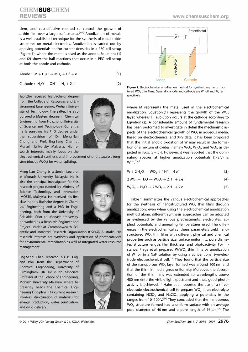
cient, and cost-effective method to control the growth ofa thin film over a large surface area.[22b] Anodization of metalsis a well-established technique for the synthesis of metal oxidestructures on metal electrodes. Anodization is carried out byapplying potentials and/or current densities in a PEC cell setup(Figure 1), where the metal is used as the anode. Equations (1)and (2) show the half reactions that occur in a PEC cell setupat both the anode and cathode.
Anode : Mþ H2O! MOx þ Hþ þ e� ð1Þ
Cathode : H2O! OH� þ H2 þ 2 e� ð2Þ
where M represents the metal used in the electrochemicalanodization. Equation (1) represents the growth of the WO3
layer, whereas H2 evolution occurs at the cathode according toEquation (2). A considerable amount of fundamental researchhas been performed to investigate in detail the mechanistic as-pects of the electrochemical growth of WO3 in aqueous media.Based on electrochemical and XPS data, it has been proposedthat the initial anodic oxidation of W may result in the forma-tion of a mixture of oxides, namely WO2, W2O5, and WO3, as de-picted in [Eqs. (3)–(5)] . However, it was reported that the domi-nating species at higher anodization potentials (>2 V) isW6 + .[13b]
Wþ 2 H2O! WO2 þ 4 Hþ þ 4 e� ð3Þ
2 WO2 þ H2O! W2O5 þ 2 Hþ þ 2 e� ð4Þ
W2O5 þ H2O! 2 WO3 þ 2 Hþ þ 2 e� ð5Þ
Table 1 summarizes the various electrochemical approachesfor the synthesis of nanostructured WO3 thin films throughanodization: even when using the electrochemical anodizationmethod alone, different synthesis approaches can be adoptedas evidenced by the various pretreatments, electrolytes, ap-plied potentials, and annealing temperatures used. The differ-ences in the electrochemical synthesis parameters yield nano-structured WO3 thin films with different physical and chemicalproperties such as particle size, surface uniformity, pore diame-ter, structure length, film thickness, and photoactivity. For in-stance, Fraga et al. prepared W/WO3 thin films by anodizationof W foil in a NaF solution by using a conventional two-elec-trode electrochemical cell.[23] They found that the particle sizeof the nanoporous WO3 layer formed was around 100 nm andthat the thin film had a great uniformity. Moreover, the absorp-tion of the thin films was extended to wavelengths above480 nm (into the visible light spectrum) and thus, good photo-activity is achieved.[23] Hahn et al. reported the use of a three-electrode electrochemical cell to prepare WO3 in an electrolytecontaining HClO4 and NaClO4 applying a potentials in theranges from 10–100 V.[24] They concluded that the nanoporousWO3 structure formed had a uniform surface with an averagepore diameter of 40 nm and a pore length of 16 mm.[24] The
Figure 1. Electrochemical anodization method for synthesizing nanostruc-tured WO3 thin films. Generally, anode and cathode are W foil and Pt, re-spectively.Tao Zhu received his Bachelor degree
from the College of Resources and En-
vironment Engineering, Wuhan Univer-
sity of Technology. Thereafter, he also
pursued a Masters degree in Chemical
Engineering from Huazhong University
of Science and Technology. Currently,
he is pursuing his PhD degree under
the supervision of Dr. Meng Nan
Chong and Prof. Eng Seng Chan at
Monash University Malaysia. His re-
search interests mainly focus on the
electrochemical synthesis and improvement of photocatalyst tung-
sten trioxide (WO3) for water splitting.
Meng Nan Chong is a Senior Lecturer
at Monash University Malaysia. He is
also the principal investigator for this
research project funded by Ministry of
Science, Technology and Innovation
(MOSTI), Malaysia. He received his first
class honors Bachelor degree in Chem-
ical Engineering and a PhD in Engi-
neering, both from the University of
Adelaide. Prior to Monash University,
he worked as a Research Engineer and
Project Leader at Commonwealth Sci-
entific and Industrial Research Organisation (CSIRO), Australia. His
research interests are synthesis and application of photocatalysts
for environmental remediation as well as integrated water resource
management.
Eng Seng Chan received his B. Eng.
and PhD from the Department of
Chemical Engineering, University of
Birmingham, UK. He is an Associate
Professor at the School of Engineering,
Monash University Malaysia, where he
presently heads the Chemical Engi-
neering Discipline. His current research
involves structuration of materials for
energy production, water purification,
and drug delivery.
� 2014 Wiley-VCH Verlag GmbH & Co. KGaA, Weinheim ChemSusChem 2014, 7, 2974 – 2997 2976
CHEMSUSCHEMREVIEWS www.chemsuschem.org

Table 1. Summary of various electrochemical synthesis approaches of WO3 thin films via anodization method.
Ref. Pretreatments Electrolyte Applied potential/current
Annealingtemperature
Morphology Photocurrent
[23] polishing of W foil using SiC sandpaperand washing with acetone, isopropanol,, water, then dried with N2
0.15 m NaF 60 V (two-elec-trode configura-tion) with ramppotential of0.2 V s�1
450 8C30 min
17 mA cm�2 at 1.5 V (vs.Ag/AgCl, KCl saturated)in 0.1 m Na2SO4 (pH 2.0)under 150 W Xe lamps
[24] degreasing of Ti and W foils by sonica-tion in acetone, isopropanol, and meth-anol; followed by rinsing with deionizedwater and drying in N2 stream; the sam-ples were pressed together using a Cu-plate contact against an O-ring
HClO4, NaClO4
(0.01, 0.05,0.1, and 1 m)
10–100 V (vs. Ag/AgCl 1 m KCl)
– – –
[22b] – 10 wt %K2HPO4 andglycerol 95 8C
50 V (two-elec-trode configura-tion) with or with-out exposure tolight source
400 8C 5 h – 2 mA cm�2 at 2.0 V (vs.Ag/AgCl 3 m KCl) in0.33 m H3PO4 under100 mW cm�2
[25] cleaning of W foils by immersion in anacetone ultrasonic bath for 10 min, fol-lowed by rinsing with deionized waterand drying in air
0.25 m oxalicacid
galvanostatic atroom temperature
350 8C inoxygen at-mosphere3 h
–
[26] sonicating W sheets in acetone, isopro-panol, and methanol successively; fol-lowed by rinsing with deionized waterand drying in a N2 stream
1 m H2SO4
and 0.5 wt %NaF
40 V (vs. Ag/AgCl1 m KCl) with a po-tential ramp1000 mV s�1
450 8C for1 h in ambi-ent air
14 mA cm�2 at 1 V (vs.Ag/AgCl) in 0.33 m
H3PO4 under oriel 6356Xe lamp
[28] degreasing of W foil by sonication inacetone, isopropanol, and methanolsuccessively; followed by rinsing in de-ionized water and drying in N2 stream
different con-centrated NaFsolution
20, 40, and 60 V(Ag/AgCl 1 m KCl)with differentperiod
– –
[9c] RF sputtering of W thin films on FTOglass
NH4F0.5 wt %/eth-ylene glycol
constant 100 W RFpower
450 8C in90 % O2 for4 h
40 mA cm�2 with nobiased voltage in 0.1 m
Na2SO4 under UV/Vis il-lumination
[8c] mechanical polishing of W foils usingSiC sandpaper; followed by anodizationin an alkaline electrolyte at a low volt-age to remove the oxide layer
1 m Na2SO4
and 0.5 wt %NaF
20, 40, and 60 V(two-electrodeconfiguration) for2 h
723 K in anoxygen at-mospherefor 3 h
0.5 mA cm�2 at 1.5 V(saturated Ag/AgCl) in0.5 m Na2SO4 under100 mW cm�2 Xe lamp
� 2014 Wiley-VCH Verlag GmbH & Co. KGaA, Weinheim ChemSusChem 2014, 7, 2974 – 2997 2977
CHEMSUSCHEMREVIEWS www.chemsuschem.org

morphology of the oxidized metal surface can be controlledby using a new electrochemical anodization under visible light.Kim et al. used the PEC anodization method for the prepara-tion of a thick WO3 film and achieved a significantly higherphotoactivity at a film thickness of 2.6 mm.[22b] In this case, thethickness of the WO3 film was double that of the WO3 film pre-pared using a conventional electrochemical anodizationmethod. The increased WO3 film thickness produced using thePEC anodization method was partly attributed to either thehigher degree of formation of crystalline outer oxide layers orthe acceleration of pore-wall dissolution at the tip of the poresdue to holes generated by illumination.[22b] Mukherjee et al.[25]
applied a constant current density for the anodization of W inoxalic acid as electrolyte and synthesized a highly regularnanoporous WO3 structure. The nanoporous WO3 structure hada smaller pore size range of 50–100 nm than that reportedfrom most sol–gel synthesis methods of W in 0.25 m oxalic acidelectrolyte.[25]
Nah et al.[26] reported the growth of nanoporous WO3 layersthrough anodization of W in a F�-containing electrolyte, whichwas later exposed to thermal treatment in NH3 for nitrogendoping. The nitrogen-doped WO3 layers exhibited photocur-rents; these were significantly improved by increased absorp-tion in the visible light region. Liu and co-workers found thatnitrogen can be doped successfully into nanoporous WO3 pho-toelectrodes by controlling the annealing temperature.[27]
Tsuchiya et al. investigated the preparation of WO3 in electro-lytes containing different concentrations of NaF in a three-elec-trode electrochemical system.[28] They found that the pores ofthe self-organized porous WO3 layers were very regular andhad an average pore diameter of 100 nm. Zheng et al.[9c] re-ported the electrochemical anodization of radio-frequency (RF)sputtered W thin films on fluorine-doped tin oxide (FTO) glassthat resulted in a uniformly structured porous WO3 films.Zhang et al. ,[8c] fabricated the nanoporous WO3 by anodizingW foil. They obtained nanoporous WO3 with an average poresize of about 80 nm and found that this WO3 nanoporousstructure had a better photoactivity under visible light in com-parison to a planar structure.[8c] Cristino et al. ,[13b] prepared
WO3 thin films obtained through method in a two-electrodeelectrochemical cell configuration. They concluded that theanodization leads to highly efficient WO3 photoanodes owingto absorption of higher wide visible spectral and electrochemi-cal active surface and improved charge-transfer kinetics undersimulated solar illumination.[13b]
2.2. Cathodic electrodeposition
Similarly, cathodic electrodeposition also allows the precisecontrol of the thickness of the nanostructured WO3 film, whichis useful for a cost-effective scale-up of processing. The catho-dic electrodeposition method is shown in Figure 2, and thevarious methods are summarized in Table 2. Other advantagesof cathodic electrodeposition include its potential for massproduction as well as the ability to produce nanostructuredWO3 thin films with large surface area-to-volume ratios.[29]
There are two different mechanisms for the cathodic electrode-position method, which are (1) the direct reduction of the oxi-dation state of metals and its deposition on the electrodes and(2) an increase in the interfacial pH value and local supersatura-tion followed by metal oxide precipitation.[12b] The latter mech-anism is usually based on the generation of a localized high-
Table 1. (Continued)
Ref. Pretreatments Electrolyte Applied potential/current
Annealingtemperature
Morphology Photocurrent
[13b] sonicating W foils in an aqueous alcoholsolution for 10 min; followed by rinsingwith water and washing with ethanoland acetone
NMF/H2O 8:2and 0.05 % w/w NH4F
40 V (two-elec-trode configura-tion) with in-creased rate at0.5 V s�1
550 8C in airfor 1 h
9 mA cm�2 at 1.7 V(SCE) in 1 m H2SO4/CH3OH 8:2 under0.120 W cm�2
[27] cleaning of W foils in four 15 min stepsin acetone, isopropanol, methanol, andfinally deionized water; followed bydrying in N2 stream
NH4/(NH4)2SO4 50 V (two-elec-trode configura-tion) for 30 min
300–650 8Cin pure N2
3.0 mA cm�2 at 1.2 V in0.5 m H2SO4 (pH 0)under 100 mW cm�2 Xelamp
Figure 2. Cathodic electrodeposition method for synthesizing WO3 thinfilms, where the cathode usually uses FTO or ITO as electrode substratewhereas Pt is employed as the anode.
� 2014 Wiley-VCH Verlag GmbH & Co. KGaA, Weinheim ChemSusChem 2014, 7, 2974 – 2997 2978
CHEMSUSCHEMREVIEWS www.chemsuschem.org

Table 2. Summary of various electrochemical synthesis approaches of WO3 thin films via cathodic method.
Ref. Precursor preparation Substrate Applied potential/cur-rent/time
Annealingtemperature/time
Morphologies Photocurrent
[37] W dissolved in H2O2 (20 %) Pt foil 3.0 V (vs. SCE)/–/– >100 8C/1 h – –[38] Na2WO4 and H2O2 at controlled
pH 1.2 (adjusted by H2SO4) toyield a ratio[H2WO4]/[H2O2] = 1:0.03.
ITO-coated glass –/1.0 mA cm2 peak cur-rent density/pulsedsquare waves with both“on” and “off” time of4.0 ms
100–400 8C/60 min
–
[39] W powder (2 g, 99 % purity) dis-solved in H2O2 (30 %; pH 2 ad-justed by H2SO4); bath tempera-ture 300 K, concentration 0.1 n
SnO2-coated plate –/0.5 mA (galvanostatic)/deposition 90 min
– – –
[17] W (2 g) powder dissolved inH2O2 (20 %) and addition ofa few drops of H2SO4
conducting trans-parent oxide(CTO)-coatedglass (10 W/&sheet resistance)
–/0.5, 0.65, and0.75 mA cm2 (galvano-static)/30–120 min
– –
[40] Na2WO4 dissolved in H2O2 (30 %;pH adjusted to 1.2 by HClO4);concentration ratio H2O2/WO4
2�
ranging from 0 to 4
F:SnO-coatedglass (NipponSheet Glass (NSG),10 W/&) andquartz oscillators
0.06 to �0.34 V vs. NHE(under Ar)/–/–
– –
[41] H2PtCl6 (0.001 m) and Na2WO4
(0.01 m) dissolved in 0.5 m H2SO4
commercial gasdiffusion layer(microporouscarbon on carboncloth)
various ranges at RT(24�2 8C) under contin-uous bubbling of N2 toeliminate O2
– –
[33] W powder (6.5 g) dissolved inH2O2 (30 %, 40 mL) and distilledwater (4 mL) at 5 8C (adjustedusing a chilled water bath whilestirring continuously) ; the Wperoxide solution was stored inthe refrigerator for ~7 days at2 8C
SnO2:F-coatedglass sheet (tradename: K-glass)
<�450 mV/1–2 mA cm2/10 min
– –
[34] Na2WO4 (25 mm) and H2O2
(0.075 %, pH adjusted to 1.4 byHNO3)
FTO-coated glassas substrate with~400 nm thickand 10.3 W/&
�0.45 V (vs. Ag/AgCl insatd. KCl)/–/25 min
350 8C/30 min
– 0.35 mA cm�2 at1.2 V (vs. Ag/AgCl insatd. KCl) in 0.1 m
Na2SO4 under 75 WXe lamp
[42] W powder (1.8 g) dissolved inH2O2 (30 %, 60 mL); followed bydecomposition of excess perox-ide using Pt black and dilutionof the solution to 50 mm usinga water/isopropanol (50:50) mix-ture or sodium dodecyl sulfate(SDS) solution
ITO-coated glass �0.2 to �0.5 V (vs. Ag/AgCl in 4 m KCl)
– 20 mA cm�2 withoutbiased voltage in0.1 m CH3OONaunder 150 W Xelamp (25 mW cm�2)
� 2014 Wiley-VCH Verlag GmbH & Co. KGaA, Weinheim ChemSusChem 2014, 7, 2974 – 2997 2979
CHEMSUSCHEMREVIEWS www.chemsuschem.org
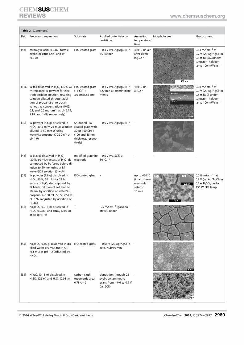
Table 2. (Continued)
Ref. Precursor preparation Substrate Applied potential/cur-rent/time
Annealingtemperature/time
Morphologies Photocurrent
[43] carboxylic acid (0.03 m ; formic,oxalic, or citric acid) and W(0.2 m)
FTO-coated glass �0.4 V (vs. Ag/AgCl)/–/15–60 min
450 8C (in airafter clean-ing)/2 h
0.14 mA cm�2 at0.7 V (vs. Ag/AgCl) in0.1 m Na2SO4/undertungsten–halogenlamp 100 mW cm�2
[12a] W foil dissolved in H2O2 (30 % w/w) replaced W powder for elec-trodeposition solution; resultingsolution diluted through addi-tion of propan-2-ol to obtainvarious W concentrations (0.05,0.1, and 0.2 mol dm�3 at pH 2.14,1.18 ,and 1.68, respectively)
FTO-coated glass(15 W/&;3.0 cm � 2.5 cm)
�0.4 V (vs. Ag/AgCl)/–/120 min at 30 min incre-ments
450 8C (inair)/2 h
0.08 mA cm�2 at0.9 V (vs. Ag/AgCl) in0.5 m NaCl undertungsten–halogenlamp 100 mW cm�2
[30] W powder (4.6 g) dissolved inH2O2 (30 % w/w, 25 mL); solutiondiluted to 50 mm W usingwater/isopropanol (70:30 v/v atpH 1.9)
Sn-doped ITO-coated glass with30 or 100 W/&(100 and 35 nmthickness, respec-tively)
�0.5 V (vs. Ag/AgCl)/–/– – –
[44] W (1.8 g) dissolved in H2O2
(30 %, 60 mL); excess of H2O2 de-composed by Pt flakes before di-lution to 50 mm using a 1:1water/SDS solution (5 wt %)
modified graphiteelectrode
�0.5 V (vs. SCE) at50 8C/–/–
– – –
[29] W powder (1.8 g) dissolved inH2O2 (30 %, 50 mL) for 24 h;excess of H2O2 decomposed byPt black; dilution of solution to50 mm by addition of water/2-propanol (~150 mL, 50:50 v/v) atpH 1.92 (adjusted by addition ofH2SO4)
ITO-coated glass – up to 450 8C(in air ; three-electrodesetup)/10 min
0.018 mA cm�2 at0.9 V (vs. Ag/AgCl) in0.1 m H2SO4 under150 W EKE lamp
[16] Na2WO4 (0.013 m) dissolved inH2O2 (0.03 m) and HNO3 (0.05 m)at RT (pH 1.4)
Ti –/5 mA cm�2 (galvano-static)/30 min
– –
[45] Na2WO4 (0.35 g) dissolved in dis-tilled water (10 mL) and H2O2
(0.1 mL) at pH 1–2 (adjusted byHNO3)
ITO-coated glass �0.65 V (vs. Ag/AgCl insatd. KCl)/10 min
– –
[32] H2WO4 (0.15 m) dissolved inH2SO4 (0.5 m) and H2O2 (0.08 m)
carbon cloth(geometric area0.78 cm2)
deposition through 25cyclic voltammetricscans from �0.6 to 0.9 V(vs. SCE)
– –
� 2014 Wiley-VCH Verlag GmbH & Co. KGaA, Weinheim ChemSusChem 2014, 7, 2974 – 2997 2980
CHEMSUSCHEMREVIEWS www.chemsuschem.org
pH region near the electrode surface, which induces the elec-trodeposition of metal ions. The mechanisms of electrodeposi-tion of WO3 can be described by two reaction steps [Eqs. (6)and (7)]:[30]
2 Wþ 10 H2O2 ! W2O112� þ 2 Hþ þ 9 H2O ð6Þ
W2O112� þ ð2þ xÞHþ þ x e� !
2 WO3 þ ð2þ xÞ=2 H2Oþ ð8�xÞ=4 O2
ð7Þ
where W2O112� corresponds to [(O2)2W(O)OW(O)(O2)2]2�and (O2)
denotes a peroxide ligand.[12a]
Meulenkamp proposed that the increase in efficiency ofnanostructured WO3 thin films was determined only to a goodapproximation by the reduction of peroxy tungstate.[30] Howev-er, the proposed mechanism strongly contradicted that ofmany other metal oxides, which are usually based on the twogeneralized mechanisms for cathodic electrodeposition dis-cussed above. In general, the nanostructured WO3 thin filmscan be cathodically electrodeposited from a solution contain-ing dissolved W.[31] During the preparation of the precursor so-lution, most researchers will decompose the excess of H2O2
used for the preparation completely by using Pt black. Contra-ry to that, Zou et al. ,[32] used cyclic voltammetry (CV) to depositpure WO3 films and found that the addition of a small volumeof H2O2 to the precursor solution facilitated the deposition ofWO3. This method led to an enhanced energy storage capacityof the composite films, especially in the negative potentialrange.[32] Apart from these advantages, cathodic electrodeposi-tion also permits the exact control of film thickness (unlike,e.g. , spin-coating) and is suitable for the fabrication of compo-site films that incorporate two or more compounds, such asWO3–CeO2, WO3–TiO2, and others.[33] For instance, Yang et al.synthesized WO3 films on indium-doped tin oxide (ITO) glassby performing the continuous cathodic electrodepositionmethod.[29] They found that the morphology of WO3 films canbe controlled by varying the H2SO4 concentration in the elec-trolyte. Vijayalakshmi and co-workers studied the effect of dif-ferent deposition current densities on the physical and chemi-cal properties of WO3 thin films.[17] At a current density of0.5 mA cm�2, they found that the surface showed no pinholesin scanning electron microscopy (SEM) images. Tacconi et al.[34]
synthesized semiconducting WO3–TiO2 composite films byusing a novel approach in cathodic electrodeposition. The pre-
Table 2. (Continued)
Ref. Precursor preparation Substrate Applied potential/cur-rent/time
Annealingtemperature/time
Morphologies Photocurrent
[46] W powder dissolved in excessH2O2 to yield peroxo-tungsticacid (0.1 m) ; addition of highpurity water and isopropyl alco-hol/ethylene glycol while stir-ring; resulting pH value of ~1.3
FTO (8–12 W/&) �600 mV (vs. Ag/AgCl) 500 8C (inair)/1 h
1.4 mA cm�2 at 1.0 V(vs. Ag/AgCl) in0.1 m CH3COONaunder 400 mW cm�2
with an AM 1.5Gfilter
[47] W powder (1 g) dissolved inH2O2 (30 % w/w, 4 mL) at pH 1.35(adjusted by HCl) ; solution wasstirred for 24 h at RT
ITO-coated glass �0.6 V vs NHE – 0.8 mA cm�2 at 1.4 V(vs. NHE) in 0.5 m
H2SO4 under0.1 W cm�2 Xe lightirradiation
[48] Na2WO4 (25 mm) and H2O2
(0.075 %) at pH 1.4; precursor forTiO2 : Ti powder dissolved in a so-lution containing H2O2 and NH3
at pH 1.7
FTO coated onsoda–lime glass
WO3/TiO2 films preparedby switching baths for5 cycles at �0.45 (forWO3) and �0.95 V (forTiO2) (vs. Ag/AgCl satd.KCl)
450 8C/30 min
1.4 mA cm�2 at 1.2 V(vs. Ag/AgCl in satd.KCl) in 0.5 m Na2SO4
under 2.2 mW cm�2
Xe arc lamp (75 W)
[35] colloidal triad solution contain-ing peroxotungstic acid (25 mm),[Ru(bpy)3]2 + (1 mm), and PSS(30 mm)
ITO-coated glass �0.45 V (vs. Ag/AgCl) – –
� 2014 Wiley-VCH Verlag GmbH & Co. KGaA, Weinheim ChemSusChem 2014, 7, 2974 – 2997 2981
CHEMSUSCHEMREVIEWS www.chemsuschem.org

cursor solution was prepared by using 25 mm Na2WO4 and0.075 % H2O2 at pH 1.4 whereas the precursor solution for TiO2
was prepared by dissolving Ti powder in a solution containingH2O2 and NH3 at pH 1.7. They found that the composite filmscontained comparable amounts of WO3 and TiO2, whichshowed superior PEC performance in 0.1 m Na2SO4 relative tothe pure metal oxides.[34] Yagi et al.[35] fabricated a hybrid WO3/[Ru(bpy)3]2+/PSS (bpy = tris(2,2’-bipyrizine) PSS = poly(sodium4-styrensufonate)) film by electrodeposition from a colloidaltriad solution containing 25 mm peroxotungstic acid, 1 mm
[Ru(bpy)3]2+ , and 30 mm PSS at a potential of �0.45 V (vs. Ag/AgCl). They found that the film thickness was constant (0.62�0.026 mm) and that the maximum absorption was at lmax =
459 nm. Zhao et al.[36] investigated the WO3/Ag–Bi photocata-lyst and found that the photocatalyst showed excellent catalyt-ic activity for water splitting. The WO3/Ag–Bi photocatalystshowed a high O2 evolution rate of 30.85 mmol h�1, a high fara-daic efficiency of 91.3 %, and a low O2 evolution overpotentialof 290 mV.
Organic and inorganic nanocomposite films have also beenwidely studied. Wei et al.[16] synthesized WO3/p-Cu2O(p=positive type) and WO3/n-Cu2O(n=negative type)composite films with consecutive cathodic electrodepositionon Ti substrates. They found that the WO3/p-Cu2O exhibiteda higher photoactivity compared to the activities of WO3 andp-Cu2O. They also found that the photoactivity of WO3/n-Cu2Owas higher than that of pure WO3 but lower than that of n-Cu2O alone.[16] Yin et al. employed the cathodic electrodeposi-tion method to produce WO3/poly-3-methoxythiophene(PMOT) films on ITO-coated glass.[45] Their results showed thatthe WO3/PMOT nanocomposite films consisted of two distinctlayers : (1) substrate WO3 layer with 30 nm grain size and (2) su-perstratum PMOT layer with an average grain size of 60 nm.
Most often, the low-cost material WO3 nanocomposite thinfilms formed using the cathodic electrodeposition method arelimited by their relatively high electrical resistivity.[49] However,this problem can be resolved by doping foreign elements intothe lattice structure of WO3. Mart�n et al. prepared electrode-posited Pt–WO3 films from a fresh solutions 0.011 m H2PtCl6,0.01 m Na2WO4 in 0.5 m H2SO4 by using a commercial gas diffu-sion electrode (e.g. , microporous carbon on carbon cloth) asworking electrode.[41] They concluded that a decrease in theelectroactive area of Pt will increase the internal resistance ofthe cell, which will eventually lead to a reduction in the PECwater splitting efficiency.
Monk and Chester prepared the cathodic electrodepositionsolution by dissolving W powder in H2O2 solution.[37] Their re-sults showed that the diffusion coefficients of intercalatingions do not vary greatly with film composition. They also con-cluded that the charge transfer resistances are dramatically af-fected by the film composition. Contrarily, Yu et al. argued thatthe cathodic electrodeposition synthesis method was very diffi-cult and time-consuming as the synthesized thin films wereslightly gelatinous and fragile.[38] Pauporte developed a simpleand fast method for preparing the cathodic electrodepositionsolution by dissolving Na2WO4 in high-purity water and byadding 30 % H2O2 in a conventional three-electrode electro-
chemical cell.[40] The WO3 thin films formed were found to beamorphous, well surface covering, and dense up to 10 nmwhile also exhibiting an increased porosity at higher film thick-nesses.
In addition, there are also other novel electrodeposition ap-proaches reported in the literature. Leftheriotis and Yianoulisprepared the cathodic electrodeposition solution by storingthe tungsten peroxide solution in a refrigerator for aboutseven days at 2 8C.[33] They obtained WO3 films with modifiedmorphologies of 1300 nm thickness. They also concluded thatWO3 films synthesized after 48 h of precursor preparation re-sults in a higher effective surface area. Baeck et al. proposeda novel electrochemical synthesis approach for the synthesis ofnanostructured WO3 thin films whereby they obtained meso-porous WO3 films with lamellar structure that showed higherphotoactivity and greater current density for hydrogen interca-lation compared to nonporous WO3.[42] Feng et al. synthesizedmesoporous WO3 films based on a one-step electrodepositionapproach.[44] They concluded that the presence of mesoporousWO3 films greatly enhanced protein loadings,which illustratedthat this type of film can provide high active surface area.
3. Effects of Synthesis Parameters on Nano-structures of WO3
3.1. Metal oxide precursor
The metal oxide precursors used in the electrochemical synthe-sis route can significantly affect the morphology of nanostruc-tures WO3 films. Shen et al. ,[31] found that WO3 films electrode-posited from solutions containing an alcohol were more stablethan the solutions without alcohols. Tsuchiya et al. synthesizedWO3 films by anodization in NaF-containing electrolytes.[28]
They found that the morphology of WO3 films was strongly af-fected by the NaF concentration in the precursor solution(Figure 3). Etching of the resulting metal oxide layers increasedwith increasing NaF concentration, causing the pores to coa-
Figure 3. Plan-view SEM images of the porous layers formed at 60 V in vari-ous NaF electrolytes: a) 0.1, b) 0.2, c) 0.5, and d) 1.0 wt %. Reprinted fromRef. [28] .
� 2014 Wiley-VCH Verlag GmbH & Co. KGaA, Weinheim ChemSusChem 2014, 7, 2974 – 2997 2982
CHEMSUSCHEMREVIEWS www.chemsuschem.org
lesce as well as the oxide layers to exhibit a mesh-like struc-ture.[28] Watcharenwong et al. prepared WO3 films by anodiza-tion using different precursors and found that 0.15 m NaF willresult in nanoporous WO3 films; 0.3 m oxalic acid will causeWO3 films to be partially or totally eroded; and PEG:H2O(PEG = polyethylene glycol) will form aggregated WO3 films.[13c]
Zhang et al. found that the presence of NaF is beneficial forthe formation of regular self-assembled nanoporous WO3 struc-tures, whereas planar films can be obtained without fluorideunder the same anodization conditions.[8c]
The electrodeposition efficiency is also strongly influencedby the composition of precursors. Kondrachova et al. foundthat the efficiency of electrodeposition from a peroxo-poly-tungstate solution strongly depended on the composition ofthe precursors.[50] Apart from this, Yang et al. , also found thatthe pH value of precursors played an important role in modify-ing the surface morphology of nanostructured thin films(Figure 4).[29] In their study, two different film types were ob-
tained at three different pH values. A mesoporous WO3 filmformed when performing the electrodeposition under cyclicvoltammetry (i.e. , �0.8 to 0.2 V, 50 mV s�1, three cycles) froma strongly acidic solution (pH 0.8; adjusted by using H2SO4).They found that the optimum pH range to prepare mesopo-rous WO3 films was between pH 0.8–1.1, whereas transparentWO3 films were electrodeposited from precursor solution(pH 1.92) but without the addition of H2SO4. Compared to thetransparent WO3 films, the nanoporous WO3 films formedunder the optimum pH conditions gave rise to photocurrentdensities nearly three times that of transparent nanoporousfilms.[29]
Thermodynamically, WO3 (yellow) is reported to be stable inacidic environments. In strong acidic electrolytes, tungstatecations may be formed.[13a] Figure 5 shows that each appliedpotential represents a different region of the Pourbaix diagramin the investigation of pH influence on the behavior of W. ThePourbaix diagram shows the potential at which chemical andelectrochemical reactions may occur on an electrode surface in
a specific electrolyte as a function of the pH value.[51] The ther-modynamic stability of chemical species at various potentialsand pH ranges can also be determined from the Pourbaix dia-gram. W forms a wide range of oxides, and the most stableoxide is WO3. Other oxides formed with W are mostly the re-sults of thermal oxidation of W or reduction of WO3. Accordingto the Pourbaix diagram, the W surface at pH 2 should be pas-sivated through the formation of WO2, W2O5, or WO3. Many re-searchers have studied the dissolution of tungsten oxides inacidic solution, but thus far no general agreement on themechanism has been found. Di Paola et al. proposed a dissolu-tion model for W in acidic solutions through the formation ofintermediate species such as WO2
2+ .[52] For pH>1, passive dis-solution of W can occur owing to the conversion of speciesmore stable than WO2
2+ , such as WO42�. Anik et al. investigat-
ed the influence of the pH value on the anodic behavior ofW.[53] They suggested that at pH 1 and pH 2.6, which corre-sponds to the point of zero charge of the WO3 surface, bothH+ and H2O would assist in WO3 dissolution. When approach-ing pH 2.6, the contribution of H+-assisted dissolution dimin-ishes.[53]
Leftheriotis and Yianoulis found an aging effect for the for-mation of WO3 films after electrodeposition from the precursorsolution.[33] The WO3 films aged for 48 h after the electrodepo-sition had a considerably higher surface roughness. This wasattributed to a conglomeration process, which is the dominantmechanism leading to the formation of grape-like structuresthat directly increase the surface roughness.[33]
Berger et al. prepared nanoporous WO3 films by anodizationin 1 m H2SO4 with 0.5 wt % NaF.[55] They found that the forma-tion of the pore structure could be attributed to enhancedetching caused by F� ions in the electrolyte, leading to a self-
Figure 4. SEM images for the surfaces of a) mesoporous film prepared fromelectrolytes at pH 0.8 and b) transparent film deposited from electrolytes atpH 1.92. Reprinted from Ref. [29] .
Figure 5. Pourbaix diagram for W (25 8C, [WO42�] 10�6 mol L�1). Line a shows
the reduction equilibrium of water E0, a =�0.0591 V � pH at a H2 or O2 pres-sure of 1 bar. Line b shows the oxidation equilibrium of waterE0, b = 1.228 V�0.0591 V � pH. Reprinted from Ref. [54] .
� 2014 Wiley-VCH Verlag GmbH & Co. KGaA, Weinheim ChemSusChem 2014, 7, 2974 – 2997 2983
CHEMSUSCHEMREVIEWS www.chemsuschem.org

ordering by competition of film formation and dissolution.Contrarily, Nah et al. synthesized compact WO3 films by usingthe same method on W sheets in 1 m H2SO4 solution but with-out addition of NaF to the electrolyte solution.[56] Kwong et al.synthesized the WO3 films from peroxotungstic acid solutioncontaining different carboxylic acids (e.g. , formic, oxalic,citric).[43] They found that the photocurrent densities of WO3
films prepared with carboxylic acids dissolved in the electrolyteare greater than those of WO3 films synthesized from pure per-oxotungstic acid solution alone. The differences were attribut-ed to improvements in (1) grain size, which controls the photo-generated electron–hole transport; and (2) effective grainboundary area, which controls the number of active reactionsites and electron–hole recombination sites.[43]
3.2. Electrode substrate
Various conductive electrode substrates have been used toprovide an effective electrodeposition platform for the growthof nanostructured WO3 thin films. In general, it can be sum-marized that the chosen electrode substrate can affect thefinal electrodeposition efficiency. In addition, the surface struc-ture of the chosen electrode substrates has an impact on theeventual size, shape, and efficiency of WO3 films formed. Thus,understanding the impact of the surface structure of chosenelectrode substrates during the electrodeposition process areessential to achieve a more uniform particle size and betterdispersion of photocatalyst particles.[57]
To date, the most common electrode substrates used in theelectrochemical synthesis methods are ITO- and FTO-coatedglass electrodes. Other electrode substrates have also beenused in some studies.[57] Shen and Tseung synthesized WO3
films by performing the electrodeposition method on variouselectrode substrates including ITO-coated glass, Au foil, and Ptfoil.[31] They found that the highest surface coverage of WO3 atthe same current density and deposition charge was achievedon ITO-coated glass, followed by Au foil whereas the least cov-erage was on Pt foil. Wei and co-workers prepared WO3/n-Cu2O and WO3/p-Cu2O composite films on Ti electrode sub-strates using cathodic electrodeposition.[16] They first synthe-sized the WO3 films on Ti electrodes followed by the n-Cu2O orp-Cu2O layer. Baeck et al. also synthesized WO3 films by pulsedelectrodeposition on Ti electrodes and ITO-coated glass elec-trodes.[49] When comparing the cathodic current deposition,the nanocrystalline WO3 films on Ti electrodes showed signifi-cantly higher current densities.[49] Huang et al. fabricated WO3-doped amorphous hydrogenated carbon films on Si as elec-trode substrates by using electrodeposition.[58] They found thatthe sizes of the nanocrystalline WO3 particles were in therange of 8–12 nm and that the particles were homogeneouslyembedded in the amorphous carbon matrix. Watcharenwonget al. produced WO3 films through cathodic electrodepositionon stainless-steel electrodes for PEC experiments.[13c] Theyfound that the surface structure of stainless-steel electrodessignificantly affected the size and morphology of WO3 filmsformed. Lee et al. prepared WO3 films on polished Ti sheetsthat showed a considerably enhanced photocurrent compared
to WO3 films on unpolished and preoxidized Ti sheets.[59] Thisfinding suggested that the in situ formation of a thin WOx–TiOy
interfacial composite layer and an improved adhesion of WO3
to the polished Ti sheet played an important role in enhancingthe photoresponse.[59] Pauporte developed a simplified ap-proach for the electrodeposition of WO3 films and found thatthe mass uptake on the Au electrode, as well as the nucleationprocess and adhesiveness of the films were poor.[40] However,he also reported that such problems were not encounteredwith FTO-coated glass electrodes.
3.3. Applied potential and current density
The morphology of nanostructured WO3 films also strongly de-pends on the applied formation potential and current density.The applied potential during the anodization process is veryimportant for the formation of regular nanoporous WO3 thinfilms.[8c] Tsuchiya et al. reported the preparation of highly or-dered porous WO3 films by performing potentiostatic anodiza-tion on pure W in NaF electrolytes.[28] At higher applied poten-tials (i.e. , 40–60 V), well-structured porous arrays were ob-served on almost all film surfaces. These arrays become largerwith increasing applied potentials.[28] In addition, Watcharen-wong et al. studied the synthesis of WO3 films by anodizationat different potentials in various electrolytes.[13c] In 0.15 m NaFelectrolytes and an applied potential range of 20–60 V, the re-sulting morphologies of WO3 films were nanohole like withstructures resembling a highly porous honeycomb and largesurface areas (Figure 6). In addition, the morphology of WO3
films in oxalic acid as electrolyte changed from little etchingfeatures at 20 V to a partially carved oxide layer at 40 V, and fi-nally to a completely etched-in oxide layer with a brain-likemorphology at 60 V. However, the oxide films prepared at 80 Vin 0.3 m oxalic acid electrolyte yielded the same nanoporousstructure as those prepared from 60 V. In addition to the ap-plied potentials and current densities, the anodization timesalso affected the morphology of the WO3 films.[13c] Zhang et al.studied the anodization of W foil and found that the appliedpotentials either lower or higher than 40 V will produce nano-porous films instead of regular nonporous structures.[8c] Pau-porte controlled the applied potentials in the range of + 0.06to �0.34 V (vs. NHE) in electrodeposition experiments usinga precursor solution of 25 mm Na2WO4 and H2O2 acidified atpH 1.2 using HClO4.[40] The highest deposition efficiency wasfound for a Na2WO4/H2O2 ratio of 0.8 and a deposition poten-tial of �0.24 V (vs. NHE). De Tacconi et al. electrodepositedWO3 and WO3–TiO2 composite films by pulsed electrical poten-tials at �0.45 and �0.95 V, respectively.[34] At �0.45 V, it was re-vealed that the pulsed potential promoted the incorporationof more TiO2 into the composite films whereas the more nega-tive pulsed potential resulted in only a negligible amount ofTiO2 in the composite film.[34]
It was also determined that different applied current densi-ties could also affect the structure of WO3 formed during theanodization. For instance, Mukherjee et al. prepared WO3 filmsunder galvanostatic anodization in a 0.25 m oxalic acid electro-lyte and found that a nonporous film was formed at a current
� 2014 Wiley-VCH Verlag GmbH & Co. KGaA, Weinheim ChemSusChem 2014, 7, 2974 – 2997 2984
CHEMSUSCHEMREVIEWS www.chemsuschem.org

density of 2.75 mA cm�2.[25] However, it was noted that the filmbehavior changed as the current density increased. At5.86 mA cm�2, a porous WO3 film was observed and the porosi-ty increased when the current was increased to 6.06 mA cm�2.At the optimum current density of 6.94 mA cm�2, the entireWO3 film was transformed into a completely porous structure.A further increase in current density beyond 9.74 mA cm�2 re-sulted only in enlarged pores to (>100 nm).[25]
It is also important to understand the implications of the dif-ferent potential modes on the formation of nanostructuredWO3 films prepared by either sweeping or stepping potentialmodes. These potential modes will influence the physical prop-erties of the metal oxide layers formed in terms of their densi-ty, porosity, and defects. When the sweeping potential mode(mild anodization) to relatively high formation potentials (upto 80 V) is applied, the formation of compact TiO2 and WO3
layers with thicknesses proportional to the applied potentialsare observed. However, when the stepping mode is used,a completely different physiochemical process occurs. For in-stance, breakdown of WO3 films takes place as a result of thehigh field strengths caused by the high applied potentials. Asa direct effect, the formation of nanostructures was evident.[24]
In an other study, Berger et al. obtained porous WO3 layers
through anodization at 40 V (measured against Ag/AgCl) for1 h at a scan rate of 1000 mV s�1 in an electrolyte containingH2SO4 and NaF.[55] The synthesized WO3 film showed a photo-current efficiency significantly higher than a compact WO3
layer with comparable light absorption length. In general, itwas observed that WO3 films of good adherence was obtainedwhen electrodeposited at relatively low potentials. In addition,it was reported that the charge density is a function of the ap-plied potential during the electrodeposition of MoxW1�xO3
films on ITO-coated glass electrodes. Kondrachova et al. ,[50] ob-served that the electrodeposition rates of Mo from the precur-sor solution increased at more negative potentials.[50] Vijaya-lakshmi[17] prepared WO3 films by galvanostatic deposition atconstant current densities of 0.50, 0.65, and 0.75 mA cm�2.Their results showed that the X-ray diffraction (XRD) peaksmeasured at 2q= 26.88 and 45.308 attenuated with increasingcurrent densities. In their study, they observed that the XRDpeak measured at 0.50 mA cm�2 was reduced in intensity at0.65 mA cm�2 whereas no prominent XRD peak was detectedat 0.75 mA cm�2.
Other effects of applied current density include the changesbrought onto the weight ratio of W:O, as well as the band gapenergy of nanostructured WO3 films formed. It was found thatthe optical band gap energy for nanostructured WO3 films de-creased from 3.2 to 2.5 eV with current density increasing from0.50 to 0.75 mA cm�2.[17]
3.4. Annealing temperature
Annealing is required to transform the WO3 film electrodepos-ited on the electrode substrate into a well-crystallized WO3
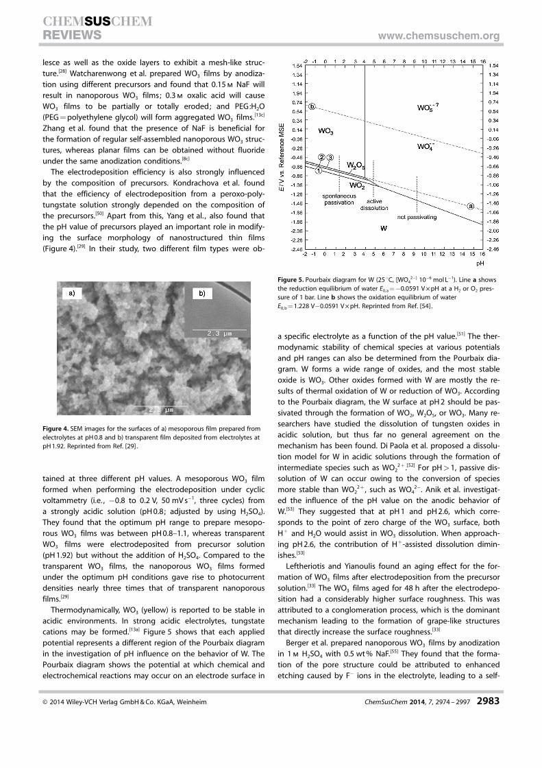
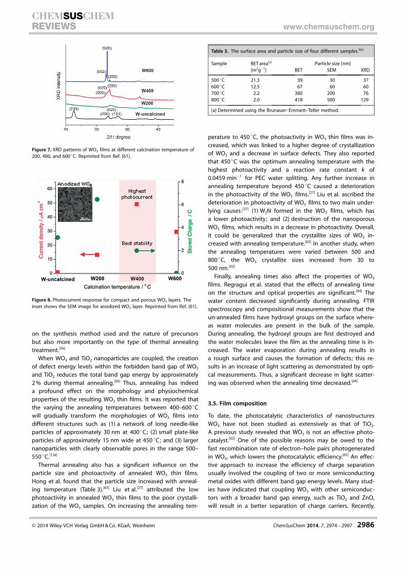
film. Such a transformation process usually occurs at the ex-pense of decreasing surface area and active sites for subse-quent photocatalytic reactions.[60] When the electrodepositedWO3 film is subjected to different annealing temperatures, thefollowing phase transitions occur: triclinic (as-electrodeposit-ed)!amorphous (100 8C)!triclinic (250 8C)!hexagonal(500 8C). After the electrodeposition process, the WO3 filmlayers could be transformed into a monoclinic structure bythermal annealing.[56] Ng et al. determined the degree of crys-tallinity of the WO3 electrodes annealed at different tempera-ture and showed that the photocurrents and charge storedchanged with the degree of crystallinity (Figures 7 and 8).[61] Itwas also observed that upon applying annealing temperaturesat 250 and 500 8C, the morphology of WO3 films will change torod-, sheet-, and fibril-like structures.[55] Nah et al. assumed thatboth compact WO3 (c-WO3) and porous WO3 (p-WO3) have anamorphous structure and that they could be converted to themonoclinic WO3 phase upon annealing.[56] While the annealingof c-WO3 film layer caused a strong increase in the responsetime, the p-WO3 film layer remained virtually unaffected by thecrystallization process.[56] In addition, the change of the amor-phous WO3 layer to a monoclinic WO3 layer on annealing at500 8C was reported to significantly increase the photocurrentconversion efficiency as well as decrease the band gapenergy.[55] In another study, it was reported that the shift in ab-sorption edge of WO3/TiO2 nanoparticles depended not only
Figure 6. Effect of anodization voltage on the morphology of nanoporousWO3 films as probed by SEM. The films were grown in 0.15 mol L�1 NaF for3 h at a) 20, b) 40, and c) 60 V, respectively. Reprinted from Ref. [13c] .
� 2014 Wiley-VCH Verlag GmbH & Co. KGaA, Weinheim ChemSusChem 2014, 7, 2974 – 2997 2985
CHEMSUSCHEMREVIEWS www.chemsuschem.org
on the synthesis method used and the nature of precursorsbut also more importantly on the type of thermal annealingtreatment.[56]
When WO3 and TiO2 nanoparticles are coupled, the creationof defect energy levels within the forbidden band gap of WO3
and TiO2 reduces the total band gap energy by approximately2 % during thermal annealing.[56] Thus, annealing has indeeda profound effect on the morphology and physiochemicalproperties of the resulting WO3 thin films. It was reported thatthe varying the annealing temperatures between 400–600 8Cwill gradually transform the morphologies of WO3 films intodifferent structures such as (1) a network of long needle-likeparticles of approximately 30 nm at 400 8C; (2) small plate-likeparticles of approximately 15 nm wide at 450 8C; and (3) largernanoparticles with clearly observable pores in the range 500–550 8C.[13a]
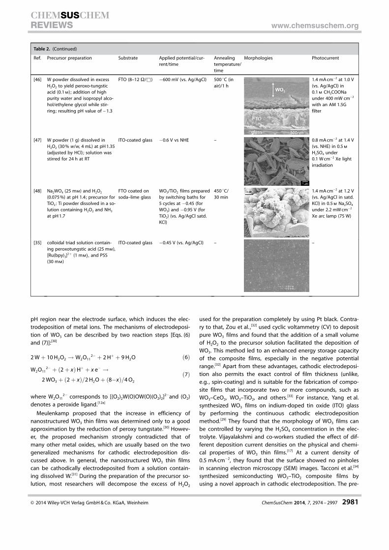
Thermal annealing also has a significant influence on theparticle size and photoactivity of annealed WO3 thin films.Hong et al. found that the particle size increased with anneal-ing temperature (Table 3).[63] Liu et al.[27] attributed the lowphotoactivity in annealed WO3 thin films to the poor crystalli-zation of the WO3 samples. On increasing the annealing tem-
perature to 450 8C, the photoactivity in WO3 thin films was in-creased, which was linked to a higher degree of crystallizationof WO3 and a decrease in surface defects. They also reportedthat 450 8C was the optimum annealing temperature with thehighest photoactivity and a reaction rate constant k of0.0459 min�1 for PEC water splitting. Any further increase inannealing temperature beyond 450 8C caused a deteriorationin the photoactivity of the WO3 films.[27] Liu et al. ascribed thedeterioration in photoactivity of WO3 films to two main under-lying causes:[27] (1) W2N formed in the WO3 films, which hasa lower photoactivity; and (2) destruction of the nanoporousWO3 films, which results in a decrease in photoactivity. Overall,it could be generalized that the crystallite sizes of WO3 in-creased with annealing temperature.[63] In another study, whenthe annealing temperatures were varied between 500 and800 8C, the WO3 crystallite sizes increased from 30 to500 nm.[62]
Finally, annealing times also affect the properties of WO3
films. Regragui et al. stated that the effects of annealing timeon the structure and optical properties are significant.[64] Thewater content decreased significantly during annealing. FTIRspectroscopy and compositional measurements show that theun-annealed films have hydroxyl groups on the surface where-as water molecules are present in the bulk of the sample.During annealing, the hydroxyl groups are first destroyed andthe water molecules leave the film as the annealing time is in-creased. The water evaporation during annealing results ina rough surface and causes the formation of defects; this re-sults in an increase of light scattering as demonstrated by opti-cal measurements. Thus, a significant decrease in light scatter-ing was observed when the annealing time decreased.[64]
3.5. Film composition
To date, the photocatalytic characteristics of nanostructuresWO3 have not been studied as extensively as that of TiO2.A previous study revealed that WO3 is not an effective photo-catalyst.[63] One of the possible reasons may be owed to thefast recombination rate of electron–hole pairs photogeneratedin WO3, which lowers the photocatalytic efficiency.[65] An effec-tive approach to increase the efficiency of charge separationusually involved the coupling of two or more semiconductingmetal oxides with different band gap energy levels. Many stud-ies have indicated that coupling WO3 with other semiconduc-tors with a broader band gap energy, such as TiO2 and ZnO,will result in a better separation of charge carriers. Recently,
Figure 7. XRD patterns of WO3 films at different calcination temperature of200, 400, and 600 8C. Reprinted from Ref. [61] .
Figure 8. Photocurrent response for compact and porous WO3 layers. Theinset shows the SEM image for anodized WO3 layer. Reprinted from Ref. [61] .
Table 3. The surface area and particle size of four different samples.[62]
Sample BET area[a] Particle size [nm][m2g�1] BET SEM XRD
500 8C 21.3 39 30 37600 8C 12.5 67 60 60700 8C 2.2 380 200 76800 8C 2.0 418 500 129
[a] Determined using the Brunauer–Emmett–Teller method.
� 2014 Wiley-VCH Verlag GmbH & Co. KGaA, Weinheim ChemSusChem 2014, 7, 2974 – 2997 2986
CHEMSUSCHEMREVIEWS www.chemsuschem.org
the coupling of WO3 with semiconductors having lower bandgap energies has attracted considerable attention; these in-clude CaFe2O4 (1.85 eV), Fe2O3 (1.97 eV), BiVO4 (2.4 eV), CuBi2O4
(1.5 eV), and CdS (2.25 eV).[16] In a composite semiconductorwith a bilayer structure, the amount (or thickness) of coating,usually the upper layer of the composite film, plays an impor-tant role in enhancing the photoactivity. Saito et al. synthe-sized a very thin SnO2 layer sandwiched between BiVO4 andWO3 layers in a carbonate electrolyte and found that the solarenergy conversion efficiency reached approximately 0.9–1.35 %using single- or double-stacked photoanodes, respectively.[66]
They also found that the photocurrent was further enhancedby the insertion of SnO2 sandwich layer (Figure 9). Mi et al. re-
ported stable intercalation compounds with the compositionxN2·WO3 (x = 0.034–0.039).[10a] The compound was formed bytrapping N2 in WO3; they also established that WO3 intercalat-ed with N2 gas exhibited a narrower band gap than pureWO3.[10a]
De Tacconi et al. prepared WO3/TiO2 thin films usinga pulsed deposition technique and found that the resultingcomposite films had a superior PEC performance in 0.1 m
Na2SO4 relative to the individual component oxides of WO3
and TiO2.[34] The incident photon-to-electron conversion effi-ciency (IPCE)[21c, 67] was determined by the mathematical ex-pression given by Equation (8):
IPCE ¼ ½1240� Il� P
� � 100 % ð8Þ
where l (nm) is the wavelength of incident light, P (mW cm�1)is the illumination power density at the specific wavelengthand I (mA cm�1) is the measured short circuit photocurrentdensity at the same wavelength. In this study, the IPCE for theWO3/TiO2 composite films was double that of its parent indi-vidual component oxides in the range 250–320 nm. The in-crease in IPCE was mainly attributed to the spatial separationof photogenerated electron–hole pairs, which resulted in mini-mal recombination of electron–hole pairs. Other contributionssuch as interparticle connection and electron percolation path-
ways in the WO3/TiO2 composite films were also considered asreasons for the enhanced IPCE. Moreover, the element ratio ofthe composite also has a strong effect on the photocatalyticactivity. Leonard et al. found that adding 9 % Zn to W resultedin a over 2.5-fold increase in photocurrent for both sulfite andwater oxidation (Figure 10).[68] Yagi et al. reported a unique ap-proach for the synthesis of WO3/[Ru(bpy)3]2+/PSS compositefilms, that is, simple electrodeposition from a colloidal solutioncontaining peroxotungstic acid and [Ru(bpy)3]2+ stabilized byPSS.[69] Kondrachova et al. prepared mixed Mo–WO3 films ofvarying stoichiometric ratios through cathodic electrodeposi-tion on ITO-coated glass electrodes from aqueous peroxo-poly-molybdotungstate solutions.[50] Liu et al. prepared WO3 byanodization prior to doping with N by annealing the WO3 filmsin NH3/N2.[27] They found that the IPCE of N-doped nanoporousWO3 films showed a significant enhancement in the energyconversion efficiency under visible light. This showed that themodification of WO3 films with N could improve the waterelectrolysis process. In another study, it was found that themodification of WO3 films with Ag–Bi resulted in a reductionof the band gap energy. They observed that the O2-evolvingoverpotential decreased from 318 to 290 mV at a current den-sity of 1 mA cm�2. In this instance, WO3 played an importantrole in improving the performance of the Ag–Bi catalyst foroxygen evolution and, thus, resulted in an improved photoac-tivity in the composite WO3/Ag–Bi films.[36] Wei et al. synthe-sized WO3/n-Cu2O and WO3/p-Cu2O composite films by consec-utive cathodic electrodeposition and found that the photoac-tivity of WO3/p-Cu2O was higher than that of pure WO3 and p-Cu2O alone.[16] On the other hand, the photoactivity of WO3/n-
Figure 9. I–V curves of multicomposite film, bare BiVO4, and bare WO3 pho-toelectrodes: a) BiVO4/SnO2/WO3, b) BiVO4/WO3, c) bare BiVO4, d) bare WO3 in0.1 m KHCO3 aqueous solution, and e) BiVO4/SnO2/WO3 in 0.1 mol L�1 Na2SO4
aqueous solution. Reprinted from Ref. [66].
Figure 10. SECM images for the typical photocurrent response of Zn/WO3
composites a) under full UV irradiation and b) with a 420 nm long-pass filter.The color represents the measured photocurrent shown in the scale barbelow each SECM image. Also shown is a schematic depicting the amountof Zn (in percent) in each spot in the array electrode. The photocurrentshown is for sulfite oxidation (0.1 mol L�1 Na2SO4 + 0.1 mol L�1 Na2SO3 atpH 7) measured at an applied potential of + 0.2 V vs Ag/AgCl. Reprintedfrom Ref. [68] .
� 2014 Wiley-VCH Verlag GmbH & Co. KGaA, Weinheim ChemSusChem 2014, 7, 2974 – 2997 2987
CHEMSUSCHEMREVIEWS www.chemsuschem.org

Cu2O was higher than that of pure WO3 but lower than n-Cu2O.
Figure 11 shows a diagram of the charge-transfer process inWO3/n-Cu2O composite films. Thermodynamically, the photo-generated electrons are transferred from the conduction bandof n-Cu2O to that of WO3 in the WO3/n-Cu2O composite films;
this made it impossible for the adsorbed O2 to consume thetransferred electrons. Therefore, the WO3/n-Cu2O compositefilms exhibited a lower photoactivity than n-Cu2O alone. As forthe WO3/p-Cu2O composite films, the charge-transfer processcould be explained by the p–n photochemical diode in Fig-ure 11 B. The majority of electrons in WO3 and holes in p-Cu2Orecombine by charge transfer through the interfaces betweenthe two semiconductors, but the recombination of the photo-generated charges in the respective semiconductors is sup-pressed. Thus, the photogenerated electrons with strong re-duction power will accumulate in the conduction band (Cu2O)as well as leave the relative photogenerated holes with strongoxidation power in the valence band (WO3).
Leonard et al. studied the space-charge capacitance by elec-trochemical impedance spectroscopy to obtain Mott–Schottkyplots based on WO3 films (Figure 12).[68] They obtained flatband potentials of each semiconductor material using the
Mott–Schottky equation at 298 K. The flat band potential couldbe estimated from the x-axis intercept of the linear portion ofthe Mott–Schottky plots. An average of the x-axis intercepts, atthree different frequencies, produced flat band potentials forWO3 that were determined to be 0.64 V (vs. NHE, with an esti-mated precision of �0.1 V). As is frequently the case, flat bandpotentials obtained from Mott–Schottky plots show a frequencydependency that may originate from surface roughness orfrom the many grain boundaries in the drop-cast semiconduc-tor films.
Wang et al. reported that the photostability and photoactivi-ty of WO3 for water oxidation can be simultaneously enhancedby controlled introduction of oxygen vacancies into WO3 ina H2 atmosphere at elevated temperatures.[70] To investigatethe effect of hydrogen treatment on the electronic propertiesof WO3, they measured the electrochemical impedance and de-rived the capacitances for the Mott–Schottky plot shown inFigure 13. In general, samples show positive slopes in theMott–Schottky plots for n-type semiconductors. The hydrogen-treated WO3 samples show substantially smaller slopes com-pared to the untreated WO3 sample, suggesting significantlyincreased donor vacancies densities based on the Mott–Schott-ky equation. The enhanced donor density is attributed to theintroduction of oxygen vacancies, which serve as shallow elec-tron donors, which improves the charge transport in WO3�x
and at the interface between substrate and WO3�x. Further-more, the capacitance of pristine WO3 reaches a plateau ataround 0.2 V (vs. Ag/AgCl), which suggests that the depletionlayer does not increase with further increase of applied poten-tial. This explains the saturation of the photocurrent density ataround 0.2 V (vs. Ag/AgCl). There is a also negative shift of theflat band potential in the H2-treated samples, possible causedby the substantially increased donor density that shifts theFermi level of WO3 upward. Additionally, the contribution ofthe Helmholtz layer capacitance becomes significant when thedonor density of WO3 increases by three orders of magnitudeincrease, which will cause a negative shift of the flat band po-tential in the Mott–Schottky plot as well.
Figure 11. Schematic diagrams for charge-transfer process in a) WO3/n-Cu2Ocomposite film and b) WO3/p-Cu2O composite film. Reprinted from Ref. [16] .
Figure 12. Mott–Schottky plot at frequencies of 200, 500, and 1000 Hz forWO3 in 0.1 mol L�1 Na2SO4 at pH 7 obtained from electrochemical impedancespectroscopy. The x-intercept of the linear region (black lines) shows themeasured flat-band potential. Reprinted from Ref. [68] .
Figure 13. Mott–Schottky plot for WO3 and hydrogen-treated WO3 sampleprepared at 350 8C and a frequency of 10 kHz in the dark. Inset: magnifiedMott–Schottky plot of the hydrogen-treated WO3. Reprinted from Ref. [70] .
� 2014 Wiley-VCH Verlag GmbH & Co. KGaA, Weinheim ChemSusChem 2014, 7, 2974 – 2997 2988
CHEMSUSCHEMREVIEWS www.chemsuschem.org

3.6. Size and thickness
It was known from previous studies that the catalytic activityof nanostructured WO3 is also affected by the size, shape, andthickness of the photocatalyst particles.[71] Nanoscaling is an ef-fective method for increasing the energy difference betweenthe band edges and redox levels as a result of quantum sizeeffects.[72] A small WO3 crystal size enhances the photoactivityby increasing the catalytic surface area. However, a small parti-cle size also increases the rate of charge recombination due tocopious amounts of surface defects. Therefore, the optimumWO3 crystal sizes have to be a compromise between optimumcatalytic surface area and the rate of surface charge recombi-nation. Studies by Kwong et al. also supported the assumptionthat optimizing the WO3 crystal size is important for PEC watersplitting applications.[43]
In general, semiconductor nanoparticles with high photoac-tivity and strong quantum-size effect are considered to be su-perior photocatalysts.[60] It is well-established that the PECwater splitting efficiency of nanostructured WO3 can be en-hanced by improving crystallinity, grain size, film thickness, sur-face morphology, and catalytic surface area.[59] As discussed inprevious sections, different synthesis approaches will yieldnanostructured WO3 with different morphologies and struc-tures. A variety of morphologies and nanostructures can beobtained by varying the starting materials and solutionchemistry, applied potential and current density, thermal an-nealing treatment and other synthesis factors.[33]
Xu et al. determined that nanoporous WO3 films havea better PEC and photocatalytic performance than planar WO3
films.[8c] Hong et al. , synthesized monoclinic WO3 nanocrystalsvia the hydrothermal reaction followed by post-calcinationtreatment.[62] They found that the WO3 particle sizes variedfrom 30 to 500 nm as the calcination temperatures waschanged from 500 to 800 8C. In another study, the averagegrain sizes were related to the amount of hydronium ions andmolecular weight of additive.[13a] Gao et al. observed improvedphysical and chemical properties in nanostructured metal chal-cogenides owing to quantum size effects when the particlesize was reduced on the nanometer scale.[74] Previously,a number of excellent review articles on the synthesis of nano-structured metal chalcogenides with controlled particle sizeand shape have been published.[75] Generally, the size and mor-phology of a specific metal chalcogenide could be effectivelycontrolled by judicious adjustment of a number of synthesisfactors such as the type and ratio of starting reagents, reactiontemperature, reaction time, and aging period. For the hydro-thermal method, the presence of a small quantity of organic li-gands often plays a key role in determining the size, shape,and structure of the metal chalcogenides formed.[74] After thehydrothermal reaction, a high-temperature calcination treat-ment is usually used to remove the residual organic ligands,which could extensively alter the size and morphology ofnanoparticles and in turn lower their photoactivity.[76] Althoughthe reduction in particle size is beneficial for surface-depen-dent photocatalysis reactions (it leads to quadratic growth ofspecific surface area and catalytic reactive sites), it is not
always true that a smaller particle size will result in a higherPEC water splitting efficiency (Figure 14). If the featured size,particularly of a spherical particle, is comparable with the elec-tron mean free path, a strong quantum confinement effect ap-pears to increase the probability of the recombination of pho-togenerated electron–hole pairs.[65] Normally, a thin film can
prevent the scattering of light and enhance the transmittanceof light, but immobilization of the thin film form would lead tosurface area constraints. Thus, suspended catalysts usuallyhave higher surface areas than films/supported ones and theintrinsic photocatalytic activity of powders is usually higherthan that of films. Kwong et al.[12a] determined that the size ofWO3 grains is dominated by the precursor W concentrationand not by the deposition time. On the contrary, the film thick-ness depends on both precursor W concentration and deposi-tion time, and the PEC water splitting efficiency is known to in-crease with increasing film thickness. Such a positive trend inPEC water efficiency was attributed to the fact that thickerWO3 films will cause a reduction in the band gap energy whileincreasing the light absorption (Figure 15).[12a]
It was also found that the nanostructured WO3 film thick-ness could be increased with the aid of illumination. Kim et al.found that the thickness of nanostructured WO3 could be ex-tended to more than 2.6 mm by using the photochemicalanodization method, which is double the typical film thicknessobtainable by conventional anodization methods without illu-mination.[22b] Baeck et al. applied pulsed electrodeposition tosynthesize WO3 films with particle sizes between 45 and330 nm and found that the cathodic deposition voltage (�1 to�3 V) had little effect on the particle size.[49] Generally, shorterelectrodeposition pulses increased the nucleation rate for newparticles above the growth rate of existing particles, whichwould explain the observed variation in particle size(Figure 16). It was found that the particle sizes were independ-ent of the total number of electrodeposition pulses applied; itseemed to affect the WO3 film thickness but not the final parti-cle size.[49] Riboni et al. found that the size of nanoparticlesformed was a function of the W/Ti ratio and the particle thatthe size decreased with an increase in the amount of Wused.[77]
Figure 14. SEM images of a) large and b) fine WO3 particles classified fromWO3 (K). Time courses for the photocatalytic evolution of oxygen overA) WO3 (KL), B) WO3 (KF), and C) commercial WO3 (K) under irradiation(405 nm). Reprinted from Ref. [73] .
� 2014 Wiley-VCH Verlag GmbH & Co. KGaA, Weinheim ChemSusChem 2014, 7, 2974 – 2997 2989
CHEMSUSCHEMREVIEWS www.chemsuschem.org

4. Fundamental Principle of WO3-based PECWater Splitting
In general, a photocatalysis cycle is comprised of three keysteps:[78] (1) light illumination-induced transition of electronsfrom the valence band to the conduction, leaving an equalnumber of vacant holes; (2) migration of excited electrons andholes to the photocatalyst surface; and (3) reaction with ad-sorbed electron donors (D) and electron acceptors (A). Lightabsorption and the resulting photo-excitation of electron–holepairs take place when the energy of incident photons matchesor exceeds the band gap energy of semiconductor photocata-lysts. In semiconducting photocatalysts, the conduction-bandelectrons (eCB
�) possess an electrochemical chemical potentialbetween + 0.5 and �1.5 V (vs. NHE); therefore, they can act asreductants. The valence-band holes (hVB
+) usually exhibit
a strong oxidative potential be-tween + 1.0 and + 3.5 V (vs.NHE).
Initially, the energy of incidentphotons is stored in semicon-ducting photocatalysts throughphoto-excitation and is laterconverted into chemical energythrough a series of electronicprocesses and surface/interfacereactions. Theoretically, a Gibbsfree energy change DG8 of237 kJ mol�1 or 1.23 eV isneeded to drive the overall reac-tion and to account for the over-potential losses occurring atboth the anode and cathodecaused by the water splitting re-action.[80] In contrast to the ther-
modynamics of conventional catalysis, photocatalysis can pro-mote not only spontaneous reactions (DG<0) but also non-spontaneous reactions (DG>0). In the former case (DG<0),the input energy is used to overcome the activation energybarrier (Eb). In the latter case (DG>0), a part of the inputenergy is converted into chemical energy that is accumulatedin the form of reaction products or by-products. However, WO3
has strong oxidizing ability, which can be largely explained byits poor band alignment with respect to the reversible hydro-gen electrode (RHE). For this reason, a bias voltage must beapplied to the WO3 photoanode to achieve H2 evolution at thePEC cathode.[81]
In a second step, a large proportion of electron–hole pairsusually recombine, dissipating input energy in the form ofheat or light emission. To prevent the recombination of elec-tron–hole pairs, the co-catalyst strategy has generally been ap-plied, that is, loading metal co-catalysts such as Pt,[83] Pd,[84]
NiO,[85] and RuO2[86] onto the semiconductor surface or within
the lattice network. The heterojunctions formed between thehost semiconducting photocatalysts and co-catalysts providean internal electric field and/or circuit that facilitates separationof the electron–hole pairs and induces faster migration ofcharged carriers.[87] Furthermore, the presence of co-catalystsusually enables a higher conductivity and photoactivity whilelowering the overpotential of the host semiconducting photo-catalysts themselves. Thus, the co-catalysts often provide idealactive sites for photocatalytic reactions to proceed.[65]
Figure 17 shows the principle operation of WO3 as a photoca-talyst for water splitting in a PEC device setup. If WO3 is usedas the photoanode in the PEC device setup, Pt is often used asthe cathode. Upon light illumination, the electrons in the va-lence band of WO3 are promoted to the conduction band andtransferred to the cathode (Pt) with the aid of an external bias.The transferred electrons will be used at cathode to reducewater molecules into H2 and O2. Simultaneously, the oxidationof water molecules is taking place at the WO3 photoanode asthe valence band holes are transferred to the electrolyte. Tocomplete a PEC cell, three different configurations are possible
Figure 15. Optical indirect band gap (Eg) of WO3 thin films as a function of thickness (d). Reprinted from Ref. [12a] .
Figure 16. Dependence of particle size of tungsten oxide films on pulse du-ration. Error bars indicate one standard deviation above and below themean. Reprinted from Ref. [49] .
� 2014 Wiley-VCH Verlag GmbH & Co. KGaA, Weinheim ChemSusChem 2014, 7, 2974 – 2997 2990
CHEMSUSCHEMREVIEWS www.chemsuschem.org
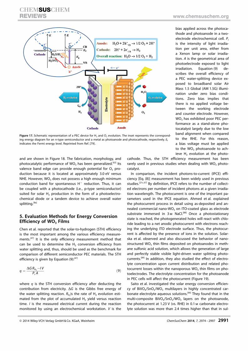
and are shown in Figure 18. The fabrication, morphology, andphotocatalytic performance of WO3 has been generalized.[63] Itsvalence band edge can provide enough potential for O2 pro-duction because it is located at approximately 3.0 eV versusNHE. However, WO3 does not possess a high enough minimumconduction band for spontaneous H+ reduction. Thus, it canbe coupled with a photocathode (i.e. , p-type semiconductor)suited for solar H2 production in the form of a photoelectro-chemical diode or a tandem device to achieve overall watersplitting.[8a]
5. Evaluation Methods for Energy ConversionEfficiency of WO3 Films
Chen et al. reported that the solar-to-hydrogen (STH) efficiencyis the most important among the various efficiency measure-ments.[47] It is the only efficiency measurement method thatcan be used to determine the H2 conversion efficiency fromwater splitting and, thus, should be used as the benchmark forcomparison of different semiconductor PEC materials. The STHefficiency is given by Equation (9):[47]
h ¼ DG RH2�I V
Pr Að9Þ
where h is the STH conversion efficiency after deducting thecontribution from electricity. DG is the Gibbs free energy ofthe water splitting reaction. RH2
is the rate of H2 evolution esti-mated from the plot of accumulated H2 yield versus reactiontime. I is the measured electrical current during the reactionmonitored by using an electrochemical workstation. V is the
bias applied across the photoca-thode and photoanode in a two-electrode electrochemical cell. Pr
is the intensity of light irradia-tion per unit area, either froma Xenon lamp or solar irradia-tion. A is the geometrical area ofphotoelectrode exposed to lightirradiation. Equation (9) de-scribes the overall efficiency ofa PEC water-splitting device ex-posed to broadband solar AirMass 1.5 Global (AM 1.5G) illumi-nation under zero bias condi-tions. Zero bias implies thatthere is no applied voltage be-tween the working electrodeand counter electrode. However,WO3 has exhibited poor PEC per-formance as a stand-alone pho-tocatalyst largely due to the lowband alignment when comparedto the RHE. For this reason,a bias voltage must be appliedto the WO3 photoanode to ach-ieve H2 evolution at the photo-
cathode. Thus, the STH efficiency measurement has beenrarely used in previous studies when dealing with WO3 photo-catalyst.
In comparison, the incident photons-to-current (IPCE) effi-ciency [Eq. (8)] measurement has been widely used in previousstudies.[21c, 67] By definition, IPCE refers to the number of collect-ed electrons per number of incident photons at a given irradia-tion wavelength. The photocurrent is one of the important pa-rameters used in the IPCE equation. Ahmed et al. explainedthe photocurrent process in detail using as-deposited and an-nealed commercial nano-WO3 on ITO-coated glass as electrodesubstrate immersed in 3 m NaCl.[88] Once a photostationarystate is reached, the photogenerated holes will react with chlo-ride leading to a net anodic photocurrent with electrons reach-ing the underlying ITO electrode surface. Thus, the photocur-rent is affected by the presence of ions in the solution. Solar-ska et al. observed and also discussed the behavior of nano-structured WO3 thin films deposited on photoanodes in meth-ane sulfonic acid solution, which allows the generation of largeand perfectly stable visible light-driven water splitting photo-currents.[89] In addition, they also studied the effect of electro-lyte concentration upon current distribution and related pho-tocurrent losses within the nanoporous WO3 thin films on pho-toelectrodes. The electrolyte concentration for the photoanodein PEC cells will affect the photocurrent (Figure 19).
Saito et al. investigated the solar energy conversion efficien-cy of BiVO4/SnO2/WO3 multilayers in highly concentrated car-bonate electrolyte aqueous solutions.[66] They found that in themulti-composite BiVO4/SnO2/WO3 layers on the photoanode,the photocurrent at 1.23 V (vs. RHE) in 0.1 m carbonate electro-lyte solution was more than 2.4 times higher than that in sul-
Figure 17. Schematic representation of a PEC device for H2 and O2 evolution. The inset represents the correspond-ing energy diagram for an n-type semiconductor and a metal as photoanode and photocathode, respectively. EF
indicates the Fermi energy level. Reprinted from Ref. [79] .
� 2014 Wiley-VCH Verlag GmbH & Co. KGaA, Weinheim ChemSusChem 2014, 7, 2974 – 2997 2991
CHEMSUSCHEMREVIEWS www.chemsuschem.org

fate electrolyte solutions. They concluded that the carbonateelectrolyte solution is very effective in the case of multi-com-posite layers on photoelectrodes as well as in the case ofa pure BiVO4 layer.[66] Ishihara et al. ,[6] found that the chemicalnature of electrolytes played a crucial role in the efficient oper-ation and energy conversion of a solar PEC cell. The interaction
between the photoelectrode and electrolyte at the interfacedepended on the electrode types. They characterized nanopo-rous WO3 structures based on their PEC properties in three dif-ferent alkaline electrolytes (NaOH-based, KOH-based, and a mix-ture of NaOH and KOH-based electrolytes) and observed differ-ent photocurrent responses.[6]
Hill and Choi[46] studied the various effects of differentanions and cations contained in an electrolyte solution on thephotocurrent conversion efficiency (Table 4). They found thatwhen CH3CO2
� and Cl� ions are present, the oxidation ofCH3CO2
� and Cl� will become the dominant photooxidation re-actions and completely suppress the O2 evolution. Whena PO4
3� solution was used, the O2 evolution and formation of
Figure 18. Three approaches to PEC solar water splitting: a) single-photo-electrode PEC cell assisted by a photovoltaic (PV) cell. Here, the photoanodeis an n-type semiconductor with a positive valence band edge relative tothe water oxidation potential. The PV cell boosts the potential of photogen-erated electrons to allow water reduction at the cathode surface. b) Two-photoelectrode PEC cell in which the photoanode and photocathode aresuitably matched n-type and p-type semiconductors assembled in parallel.c) A tandem two-photoelectrode PEC cell assembled in series, such that low-energy photons that are not absorbed by the photoanode are absorbed bythe photocathode. Reprinted from Ref. [82] .
Figure 19. A series of photocurrent–voltage plots for the same electrode illu-minated with AM 1.5 light in CH3HSO3 solutions of various concentrations: 2,1, 0.5, and 0.04 mol L�1. Reprinted from Ref. [89] .
Table 4. Summary of the photocurrent to oxygen conversion efficienciesobtained in electrolytes with very pH conditions and anions (or cat-ions).[46]
Electrolyte pH value Photocurrent-to-oxygenconversion efficiency [%]
CH3COOH 3 0CH3COONa 5 0NaCl 1 0NaCl 3 0NaCl 5 0NaH2PO4 1 33NaH2PO4 3 58NaH2PO4 5 79NaClO4 1 32NaClO4 3 29NaClO4 5 9Na2SO4 1 35Na2SO4 3 63Na2SO4 5 88Li2SO4 3 35Na2SO4 3 63K2SO4 3 79LiClO4 3 10NaClO4 3 29KClO4 3 49LiH2PO4 3 63NaH2PO4 3 67KH2PO4 3 87
� 2014 Wiley-VCH Verlag GmbH & Co. KGaA, Weinheim ChemSusChem 2014, 7, 2974 – 2997 2992
CHEMSUSCHEMREVIEWS www.chemsuschem.org
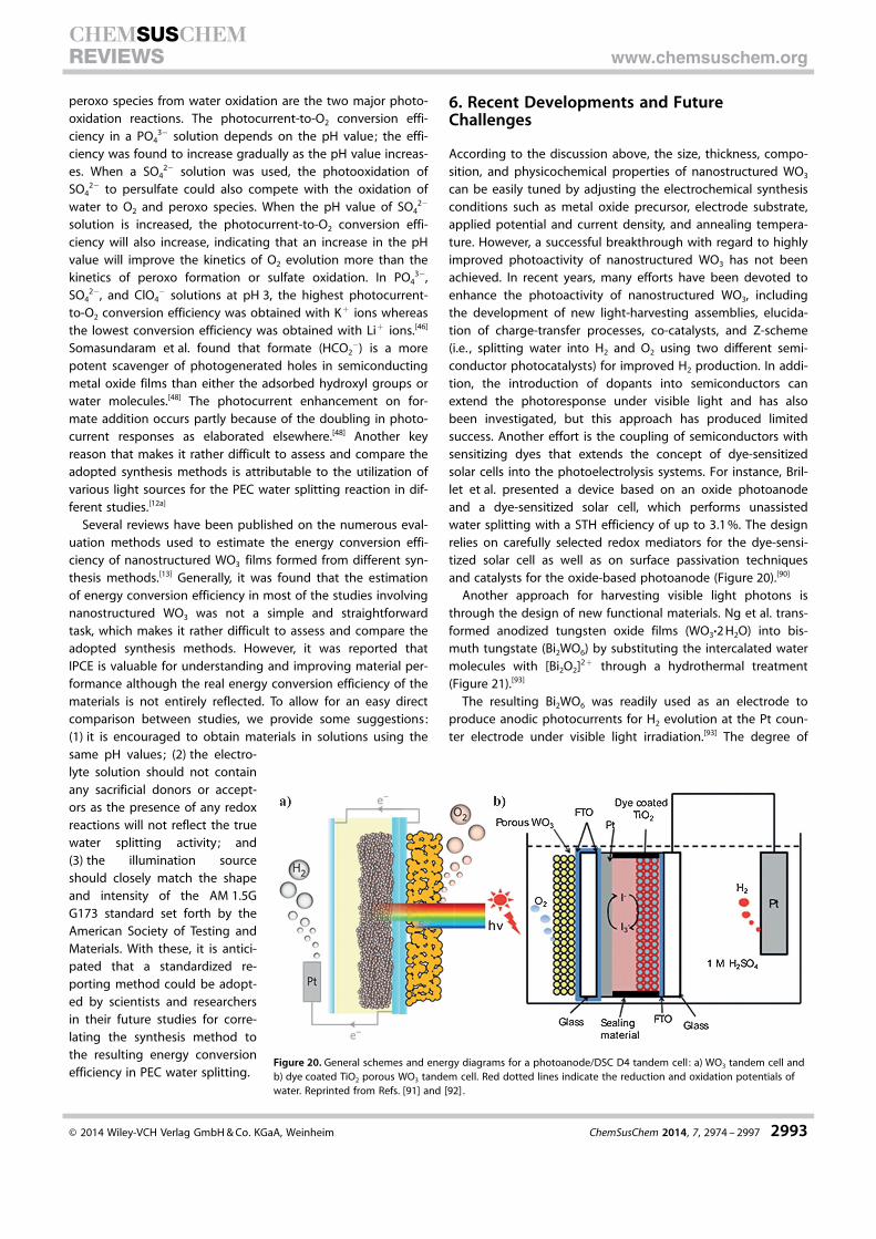
peroxo species from water oxidation are the two major photo-oxidation reactions. The photocurrent-to-O2 conversion effi-ciency in a PO4
3� solution depends on the pH value; the effi-ciency was found to increase gradually as the pH value increas-es. When a SO4
2� solution was used, the photooxidation ofSO4
2� to persulfate could also compete with the oxidation ofwater to O2 and peroxo species. When the pH value of SO4
2�
solution is increased, the photocurrent-to-O2 conversion effi-ciency will also increase, indicating that an increase in the pHvalue will improve the kinetics of O2 evolution more than thekinetics of peroxo formation or sulfate oxidation. In PO4
3�,SO4
2�, and ClO4� solutions at pH 3, the highest photocurrent-
to-O2 conversion efficiency was obtained with K+ ions whereasthe lowest conversion efficiency was obtained with Li+ ions.[46]
Somasundaram et al. found that formate (HCO2�) is a more
potent scavenger of photogenerated holes in semiconductingmetal oxide films than either the adsorbed hydroxyl groups orwater molecules.[48] The photocurrent enhancement on for-mate addition occurs partly because of the doubling in photo-current responses as elaborated elsewhere.[48] Another keyreason that makes it rather difficult to assess and compare theadopted synthesis methods is attributable to the utilization ofvarious light sources for the PEC water splitting reaction in dif-ferent studies.[12a]
Several reviews have been published on the numerous eval-uation methods used to estimate the energy conversion effi-ciency of nanostructured WO3 films formed from different syn-thesis methods.[13] Generally, it was found that the estimationof energy conversion efficiency in most of the studies involvingnanostructured WO3 was not a simple and straightforwardtask, which makes it rather difficult to assess and compare theadopted synthesis methods. However, it was reported thatIPCE is valuable for understanding and improving material per-formance although the real energy conversion efficiency of thematerials is not entirely reflected. To allow for an easy directcomparison between studies, we provide some suggestions:(1) it is encouraged to obtain materials in solutions using thesame pH values; (2) the electro-lyte solution should not containany sacrificial donors or accept-ors as the presence of any redoxreactions will not reflect the truewater splitting activity; and(3) the illumination sourceshould closely match the shapeand intensity of the AM 1.5GG173 standard set forth by theAmerican Society of Testing andMaterials. With these, it is antici-pated that a standardized re-porting method could be adopt-ed by scientists and researchersin their future studies for corre-lating the synthesis method tothe resulting energy conversionefficiency in PEC water splitting.
6. Recent Developments and FutureChallenges
According to the discussion above, the size, thickness, compo-sition, and physicochemical properties of nanostructured WO3
can be easily tuned by adjusting the electrochemical synthesisconditions such as metal oxide precursor, electrode substrate,applied potential and current density, and annealing tempera-ture. However, a successful breakthrough with regard to highlyimproved photoactivity of nanostructured WO3 has not beenachieved. In recent years, many efforts have been devoted toenhance the photoactivity of nanostructured WO3, includingthe development of new light-harvesting assemblies, elucida-tion of charge-transfer processes, co-catalysts, and Z-scheme(i.e. , splitting water into H2 and O2 using two different semi-conductor photocatalysts) for improved H2 production. In addi-tion, the introduction of dopants into semiconductors canextend the photoresponse under visible light and has alsobeen investigated, but this approach has produced limitedsuccess. Another effort is the coupling of semiconductors withsensitizing dyes that extends the concept of dye-sensitizedsolar cells into the photoelectrolysis systems. For instance, Bril-let et al. presented a device based on an oxide photoanodeand a dye-sensitized solar cell, which performs unassistedwater splitting with a STH efficiency of up to 3.1 %. The designrelies on carefully selected redox mediators for the dye-sensi-tized solar cell as well as on surface passivation techniquesand catalysts for the oxide-based photoanode (Figure 20).[90]
Another approach for harvesting visible light photons isthrough the design of new functional materials. Ng et al. trans-formed anodized tungsten oxide films (WO3·2 H2O) into bis-muth tungstate (Bi2WO6) by substituting the intercalated watermolecules with [Bi2O2]2+ through a hydrothermal treatment(Figure 21).[93]
The resulting Bi2WO6 was readily used as an electrode toproduce anodic photocurrents for H2 evolution at the Pt coun-ter electrode under visible light irradiation.[93] The degree of
Figure 20. General schemes and energy diagrams for a photoanode/DSC D4 tandem cell : a) WO3 tandem cell andb) dye coated TiO2 porous WO3 tandem cell. Red dotted lines indicate the reduction and oxidation potentials ofwater. Reprinted from Refs. [91] and [92] .
� 2014 Wiley-VCH Verlag GmbH & Co. KGaA, Weinheim ChemSusChem 2014, 7, 2974 – 2997 2993
CHEMSUSCHEMREVIEWS www.chemsuschem.org

light harvesting can be determined by the different opals WO3
used. For example, Chen et al. demonstrated that photoniccrystals could be used to improve light harvesting andphoton-to-electron conversion efficiency at specific wave-lengths by utilization of the slow-light effect in the inverseopals WO3.[94] The spectral range at which the photon-to-elec-tron conversion efficiency is enhanced is shifted to shorterwavelengths as the incident angle increases, which resultsfrom a blue shift in the stop-band center.
These findings suggest that the implementation of semicon-ducting photovoltaic devices in the form of photonic crystalsto manipulate the behavior of photons and electrons is a feasi-ble and effective way for enhancing the photon-to-electronconversion efficiency. It will also provide useful information fordeveloping other visible-light-sensitive photoanodes witha photonic crystal structure. The increase of light absorptioninduced by the slow-light effect in the WO3-200 inverse opalcan be extended to the onset of visible region, as shown inFigure 22.[94]
As for the elucidation of charge-transfer processes in nano-structured WO3, the recent developments are mainly based onthe synthesis of multilayer thin films such as TiO2/WO3/Pt,[86]
Ag/AgCl/plate-WO3,[95] Mo-BiVO4/WO3,[87] WO3/Fe2O3/WO3, andFe2O3/WO3/Fe2O3.[8a] To achieve more effective PEC-drivenwater splitting, a hybrid photoelectrode based on PEC tandemcell design was developed.[91] Figures 23 and 24 show the sum-mary of photoelectrochemical tandem cells for different photo-catalysts. In addition, heterojunction structures can also offer
enhanced separation of photogenerated charge carriers as pre-viously reported for WO3/BiVO4,[67] Bi2S3/WO3,[89] grapheneoxide-WO3,[88] and multiple (WO3-Pt)/TiO2.[89] The conductionband of WO3 is not high enough to induce H+ reduction. Theenhanced electric field produced from the photoexcitation ofa localized surface plasmon resonance (LSPR) peak of Au parti-cles has been shown to improve the photocatalytic activity asevidenced by an increase in accompanying H2 production. Theoptimal distance between Au and the semiconductor core,that is, CdS, remains an important factor in achieving a plas-mon-induced enhancement of the PEC process. Transition
Figure 21. Structural transformation of anodized WO3·2 H2O into Bi2WO6. Re-printed from Ref. [93].
Figure 22. a) Light absorption spectra of WO3 inverse opals, a disorderedporous WO3, and an unpatterned WO3 photoanode measured at a normalincidence of light. The colored hollow circles show the slow light absorptionat the red edge of the stop band for each inverse opal structure. b) Absorb-ance enhancement spectra (ratio of the absorbance of WO3 inverse opalsand disordered porous sample to that of the unpatterned WO3 photoanode)as a function of the wavelength. Reprinted from Ref. [94] .
Figure 23. Maximum solar-to-hydrogen conversion efficiency and solar pho-tocurrent as a function of the top cell band gap energy in a tandem cell.The band gap energies and efficiency range for commonly used semicon-ductor oxide photoanodes are also shown. Reprinted from Ref. [96].
Figure 24. Schematic side view of a WO3 jCdTe jWC tandem cell device andphotographs of an actual device. External wires attached to each tandemcell component (WO3, CdTe, WC) allow for measurement of the current–volt-age characteristics of either the whole device or an individual component.Reprinted from Ref. [91] .
� 2014 Wiley-VCH Verlag GmbH & Co. KGaA, Weinheim ChemSusChem 2014, 7, 2974 – 2997 2994
CHEMSUSCHEMREVIEWS www.chemsuschem.org
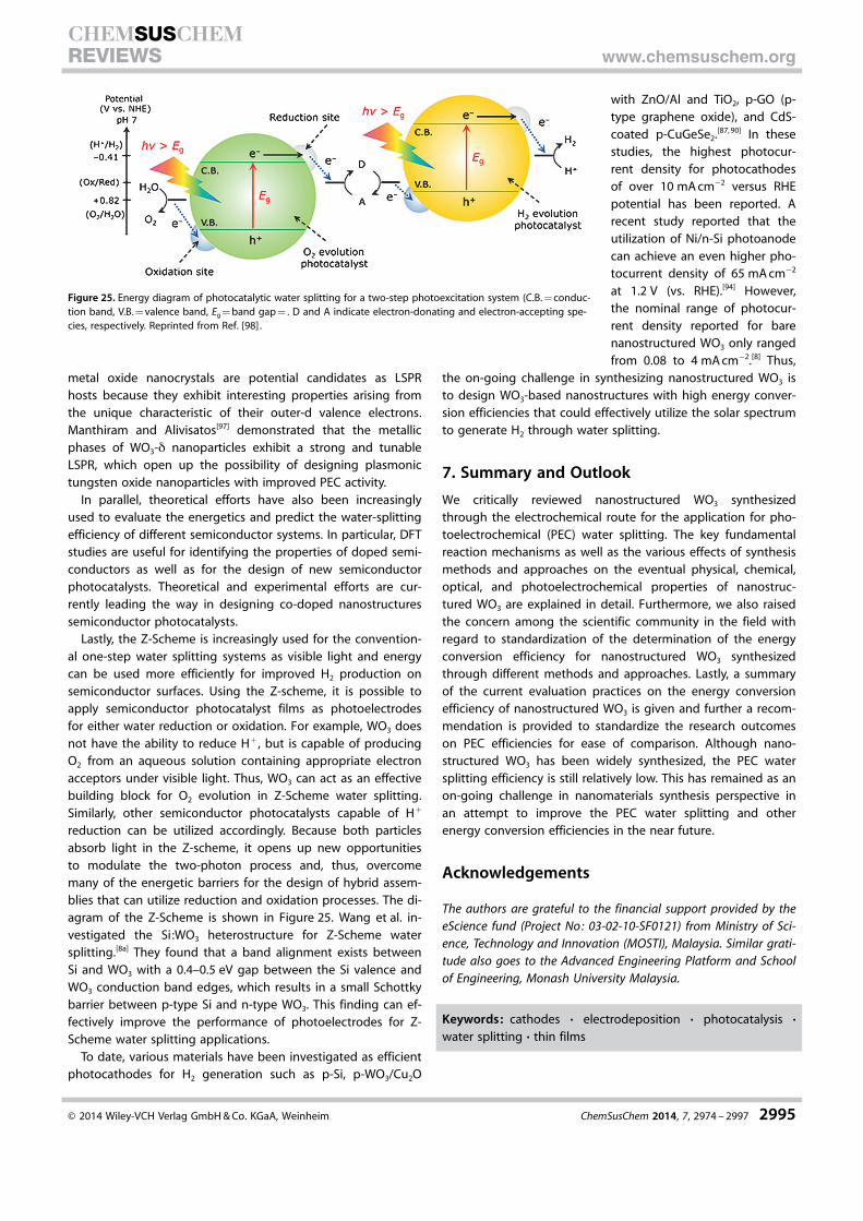
metal oxide nanocrystals are potential candidates as LSPRhosts because they exhibit interesting properties arising fromthe unique characteristic of their outer-d valence electrons.Manthiram and Alivisatos[97] demonstrated that the metallicphases of WO3-d nanoparticles exhibit a strong and tunableLSPR, which open up the possibility of designing plasmonictungsten oxide nanoparticles with improved PEC activity.
In parallel, theoretical efforts have also been increasinglyused to evaluate the energetics and predict the water-splittingefficiency of different semiconductor systems. In particular, DFTstudies are useful for identifying the properties of doped semi-conductors as well as for the design of new semiconductorphotocatalysts. Theoretical and experimental efforts are cur-rently leading the way in designing co-doped nanostructuressemiconductor photocatalysts.
Lastly, the Z-Scheme is increasingly used for the convention-al one-step water splitting systems as visible light and energycan be used more efficiently for improved H2 production onsemiconductor surfaces. Using the Z-scheme, it is possible toapply semiconductor photocatalyst films as photoelectrodesfor either water reduction or oxidation. For example, WO3 doesnot have the ability to reduce H+ , but is capable of producingO2 from an aqueous solution containing appropriate electronacceptors under visible light. Thus, WO3 can act as an effectivebuilding block for O2 evolution in Z-Scheme water splitting.Similarly, other semiconductor photocatalysts capable of H+
reduction can be utilized accordingly. Because both particlesabsorb light in the Z-scheme, it opens up new opportunitiesto modulate the two-photon process and, thus, overcomemany of the energetic barriers for the design of hybrid assem-blies that can utilize reduction and oxidation processes. The di-agram of the Z-Scheme is shown in Figure 25. Wang et al. in-vestigated the Si:WO3 heterostructure for Z-Scheme watersplitting.[8a] They found that a band alignment exists betweenSi and WO3 with a 0.4–0.5 eV gap between the Si valence andWO3 conduction band edges, which results in a small Schottkybarrier between p-type Si and n-type WO3. This finding can ef-fectively improve the performance of photoelectrodes for Z-Scheme water splitting applications.
To date, various materials have been investigated as efficientphotocathodes for H2 generation such as p-Si, p-WO3/Cu2O
with ZnO/Al and TiO2, p-GO (p-type graphene oxide), and CdS-coated p-CuGeSe2.[87, 90] In thesestudies, the highest photocur-rent density for photocathodesof over 10 mA cm�2 versus RHEpotential has been reported. Arecent study reported that theutilization of Ni/n-Si photoanodecan achieve an even higher pho-tocurrent density of 65 mA cm�2
at 1.2 V (vs. RHE).[94] However,the nominal range of photocur-rent density reported for barenanostructured WO3 only rangedfrom 0.08 to 4 mA cm�2.[8] Thus,
the on-going challenge in synthesizing nanostructured WO3 isto design WO3-based nanostructures with high energy conver-sion efficiencies that could effectively utilize the solar spectrumto generate H2 through water splitting.
7. Summary and Outlook
We critically reviewed nanostructured WO3 synthesizedthrough the electrochemical route for the application for pho-toelectrochemical (PEC) water splitting. The key fundamentalreaction mechanisms as well as the various effects of synthesismethods and approaches on the eventual physical, chemical,optical, and photoelectrochemical properties of nanostruc-tured WO3 are explained in detail. Furthermore, we also raisedthe concern among the scientific community in the field withregard to standardization of the determination of the energyconversion efficiency for nanostructured WO3 synthesizedthrough different methods and approaches. Lastly, a summaryof the current evaluation practices on the energy conversionefficiency of nanostructured WO3 is given and further a recom-mendation is provided to standardize the research outcomeson PEC efficiencies for ease of comparison. Although nano-structured WO3 has been widely synthesized, the PEC watersplitting efficiency is still relatively low. This has remained as anon-going challenge in nanomaterials synthesis perspective inan attempt to improve the PEC water splitting and otherenergy conversion efficiencies in the near future.
Acknowledgements
The authors are grateful to the financial support provided by theeScience fund (Project No : 03-02-10-SF0121) from Ministry of Sci-ence, Technology and Innovation (MOSTI), Malaysia. Similar grati-tude also goes to the Advanced Engineering Platform and Schoolof Engineering, Monash University Malaysia.
Keywords: cathodes · electrodeposition · photocatalysis ·water splitting · thin films
Figure 25. Energy diagram of photocatalytic water splitting for a two-step photoexcitation system (C.B. = conduc-tion band, V.B. = valence band, Eg = band gap = . D and A indicate electron-donating and electron-accepting spe-cies, respectively. Reprinted from Ref. [98] .
� 2014 Wiley-VCH Verlag GmbH & Co. KGaA, Weinheim ChemSusChem 2014, 7, 2974 – 2997 2995
CHEMSUSCHEMREVIEWS www.chemsuschem.org
[1] J. R. Bartels, M. B. Pate, N. K. Olson, Int. J. Hydrogen Energy 2010, 35,8371 – 8384.
[2] A. Fujishima, K. Honda, Nature 1972, 238, 37.[3] a) S. Balachandran, M. Swaminathan, J. Phys. Chem. C 2012, 116, 26306 –
26312; b) S. Chen, W. Zhao, W. Liu, S. Zhang, Appl. Surf. Sci. 2008, 255,2478 – 2484; c) H. Qin, W. Li, Y. Xia, T. He, ACS Appl. Mater. Interfaces2011, 3, 3152 – 3156.
[4] a) Q. Han, Z. H. Liu, Y. Y. Xu, Z. Y. Chen, T. M. Wang, H. Zhang, J. Phys.Chem. C 2007, 111, 5034 – 5038; b) M. Niu, F. Huang, L. Cui, P. Huang, Y.Yu, Y. Wang, ACS Nano 2010, 4, 681 – 688; c) Y. Shi, H. Li, L. Wang, W.Shen, H. Chen, ACS Appl. Mater. Interfaces 2012, 4, 4800 – 4806.
[5] a) F. Magalh¼es, F. C. C. Moura, R. M. Lago, Desalination 2011, 276, 266 –271; b) C. Shifu, Z. Sujuan, L. Wei, Z. Wei, J. Hazard. Mater. 2008, 155,320 – 326; c) V. Vimonses, M. N. Chong, B. Jin, Microporous MesoporousMater. 2010, 132, 201 – 209.
[6] H. Ishihara, G. K. Kannarpady, K. R. Khedir, J. Woo, S. Trigwell, A. S. Biris,Phys. Chem. Chem. Phys. 2011, 13, 19553 – 19560.
[7] K.-S. Ahn, S.-H. Lee, A. C. Dillon, C. E. Tracy, R. Pitts, J. Appl. Phys. 2007,101, 093524.
[8] a) S. S. Kalanur, Y. J. Hwang, S. Y. Chae, O. S. Joo, J. Mater. Chem. A 2013,1, 3479 – 3488; b) V. S. Vidyarthi, M. Hofmann, A. Savan, K. Sliozberg, D.Kçnig, R. Beranek, W. Schuhmann, A. Ludwig, Int. J. Hydrogen Energy2011, 36, 4724 – 4731; c) X. M. Zhang, K. Huo, L. Hu, P. K. Chu, IEEE Nano-electronics Conference 2010, 1090 – 1091; d) S. Yousefzadeh, A. Reyhani,N. Naseri, A. Z. Moshfegh, J. Solid State Chem. 2013, 204, 341 – 347.
[9] a) C. Cantalini, W. Wlodarski, Y. Li, M. Passacantando, S. Santucci, E.Comini, G. Faglia, G. Sberveglieri, Sens. Actuators B 2000, 64, 182 – 188;b) W. Li, C. Liu, Y. Yang, J. Li, Q. Chen, F. Liu, Mater. Lett. 2012, 84, 41 –43; c) H. Zheng, A. Z. Sadek, K. Latham, K. Kalantar-Zadeh, Electrochem.Commun. 2009, 11, 768 – 771.
[10] a) Q. Mi, Y. Ping, Y. Li, B. Cao, B. S. Brunschwig, P. G. Khalifah, G. A. Galli,H. B. Gray, N. S. Lewis, J. Am. Chem. Soc. 2012, 134, 18318 – 18324;b) K. J. Patel, C. J. Panchal, M. S. Desai, P. K. Mehta, Mater. Chem. Phys.2010, 124, 884 – 890; c) A. Ponzoni, E. Comini, M. Ferroni, G. Sberveglieri,Thin Solid Films 2005, 490, 81 – 85.
[11] a) D. Gogova, G. Stoyanov, K. A. Gesheva, Renewable Energy 1996, 8,546 – 550; b) J. Goschnick, M. Frietsch, T. Schneider, Surface and CoatingsTechnology 1998, 108 – 109, 292 – 296; c) Z. S. Houweling, J. W. Geus,R. E. I. Schropp, Mater. Chem. Phys. 2013, 140, 89 – 96.
[12] a) W. L. Kwong, N. Savvides, C. C. Sorrell, Electrochim. Acta 2012, 75,371 – 380; b) T. Pauport�, A. Goux, A. Kahn-Harari, N. de Tacconi, C. R.Chenthamarakshan, K. Rajeshwar, D. Lincot, J. Phys. Chem. Solids 2003,64, 1737 – 1742; c) I. Zhitomirsky, Adv. Colloid Interface Sci. 2002, 97,279 – 317.
[13] a) C. A. Bignozzi, S. Caramori, V. Cristino, R. Argazzi, L. Meda, A. Tacca,Chem. Soc. Rev. 2013, 42, 2228 – 2246; b) V. Cristino, S. Caramori, R. Ar-gazzi, L. Meda, G. L. Marra, C. A. Bignozzi, Langmuir 2011, 27, 7276 –7284; c) A. Watcharenwong, W. Chanmanee, N. R. de Tacconi, C. R.Chenthamarakshan, P. Kajitvichyanukul, K. Rajeshwar, J. Electroanal.Chem. 2008, 612, 112 – 120.
[14] a) K.-I. Liu, Y.-C. Hsueh, C.-Y. Su, T.-P. Perng, Int. J. Hydrogen Energy 2013,38, 7750 – 7755; b) N. Naseri, S. Yousefzadeh, E. Daryaei, A. Z. Moshfegh,Int. J. Hydrogen Energy 2011, 36, 13461 – 13472.
[15] M.-S. Gui, W.-D. Zhang, Y.-Q. Chang, Y.-X. Yu, Chem. Eng. J. 2012, 197,283 – 288.
[16] S. Wei, Y. Ma, Y. Chen, L. Liu, Y. Liu, Z. Shao, J. Hazard. Mater. 2011, 194,243 – 249.
[17] R. Vijayalakshmi, Synth. React. Inorg. Metal-Org. Nano-Metal Chem. 2006,36, 89 – 94.
[18] a) N. Sonoyama, K. Iwase, H. Takatsuka, T. Matsumura, N. Imanishi, Y.Takeda, R. Kanno, J. Power Sources 2009, 189, 561 – 565; b) M. Plaza, M.Abu�n, A. Mascaraque, M. A. Gonz�lez-Barrio, L. P�rez, Mater. Chem.Phys. 2012, 134, 523 – 530.
[19] a) P. E. Hovsepian, D. B. Lewis, Q. Luo, A. Farinotti, Thin Solid Films 2005,488, 1 – 8; b) R. Vaidyanathan, S. M. Cox, U. Happek, D. Banga, M. K.Mathe, J. L. Stickney, Langmuir 2006, 22, 10590 – 10595.
[20] a) S. Feng, J. Yang, M. Liu, H. Zhu, J. Zhang, G. Li, J. Peng, Q. Liu, Electro-chim. Acta 2012, 83, 321 – 326; b) S. Li, H. Zhao, D. Tian, Mater. Sci. Semi-cond. Proc. 2013, 16, 149 – 153.
[21] a) D. J. Comstock, S. T. Christensen, J. W. Elam, M. J. Pellin, M. C. Hersam,Electrochem. Commun. 2010, 12, 1543 – 1546; b) S. Bai, C. Sun, T. Guo, R.
Luo, Y. Lin, A. Chen, L. Sun, J. Zhang, Electrochim. Acta 2013, 90, 530 –534; c) K. Liang, X. Tang, B. Wei, W. Hu, Mater. Res. Bull. 2013, 48, 3829 –3833.
[22] a) S. Gupta, M. Tripathi, S. Gupta, M. Tripathi, M. Tripathi, Centr. Eur. J.Chem. 2011, 10, 279 – 294; b) S. Kim, J. Choi, S. Kim, J. Choi, Electrochem.Commun. 2012, 17, 10 – 13.
[23] L. E. Fraga, M. V. B. Zanoni, L. E. Fraga, M. V. B. Zanoni, J. Braz. Chem. Soc.2011, 22, 718 – 725.
[24] R. Hahn, J. M. Macak, P. Schmuki, Electrochem. Commun. 2007, 9, 947 –952.
[25] N. Mukherjee, M. Paulose, O. K. Varghese, G. K. Mor, C. A. Grimes, N. Mu-kherjee, M. Paulose, O. K. Varghese, G. K. Mor, C. A. Grimes, J. Mater. Res.2003, 18, 2296 – 2299.
[26] Y.-c. Nah, I. Paramasivam, R. Hahn, N. K. Shrestha, P. Schmuki, Nanotech-nology 2010, 21, 105704.
[27] Y. Liu, Y. Li, W. Li, S. Han, C. Liu, Appl. Surf. Sci. 2012, 258, 5038 – 5045.[28] H. Tsuchiya, J. M. Macak, I. Sieber, L. Taveira, A. Ghicov, K. Sirotna, P.
Schmuki, Electrochem. Commun. 2005, 7, 295 – 298.[29] B. Yang, H. Li, M. Blackford, V. Luca, Curr. Appl. Phys. 2006, 6, 436 – 439.[30] E. A. Meulenkamp, J. Electrochem. Soc. 1997, 144, 1664.[31] P. K. Shen, A. C. C. Tseung, J. Mater. Chem. 1992, 2, 1141 – 1147.[32] B.-X. Zou, Y. Liang, X.-X. Liu, D. Diamond, K.-T. Lau, J. Power Sources
2011, 196, 4842 – 4848.[33] G. Leftheriotis, P. Yianoulis, Solid State Ionics 2008, 179, 2192 – 2197.[34] N. R. de Tacconi, C. R. Chenthamarakshan, K. Rajeshwar, T. Pauport�, D.
Lincot, Electrochem. Commun. 2003, 5, 220 – 224.[35] M. Yagi, K. Sone, M. Yamada, S. Umemiya, Chem. Eur. J. 2005, 11, 767 –
775.[36] Q. Zhao, Z. Yu, W. Yuan, J. Li, Int. J. Hydrogen Energy 2012, 37, 13249 –
13255.[37] P. M. S. Monk, S. L. Chester, Electrochim. Acta 1993, 38, 1521 – 1526.[38] Z. Yu, X. Jia, J. Du, J. Zhang, Solar Ener. Mater. Solar Cells 2000, 64, 55 –
63.[39] R. Vijayalakshmi, M. Jayachandran, C. Sanjeeviraja, Curr. Appl. Phys.
2003, 3, 171 – 175.[40] T. Pauporte, J. Electrochem. Soc. 2002, 149, C539 – C545.[41] A. J. Mart�n, A. M. Chaparro, L. Daza, J. Power Sources 2011, 196, 4187 –
4192.[42] S. H. Baeck, K. S. Choi, T. F. Jaramillo, G. D. Stucky, E. W. McFarland, Adv.
Mater. 2003, 15, 1269 – 1273.[43] W. L. Kwong, A. Nakaruk, P. Koshy, C. C. Sorrell, Thin Solid Films 2013,
544, 191 – 196.[44] J.-J. Feng, J.-J. Xu, H.-Y. Chen, Electrochem. Commun. 2006, 8, 77 – 82.[45] H. Y. Yin, X. C. Song, Y. F. Zheng, X. Wang, Z. A. Yang, R. Ma, Mater. Sci.
Eng. B 2011, 176, 684 – 687.[46] J. C. Hill, K.-S. Choi, J. Phys. Chem. C 2012, 116, 7612 – 7620.[47] W. Zhao, Z. Wang, X. Shen, J. Li, C. Xu, Z. Gan, Int. J. Hydrogen Energy
2012, 37, 908 – 915.[48] S. Somasundaram, C. R. Chenthamarakshan, N. R. de Tacconi, N. A. Basit,
K. Rajeshwar, Electrochem. Commun. 2006, 8, 539 – 543.[49] S. H. Baeck, T. Jaramillo, G. D. Stucky, E. W. McFarland, Nano Lett. 2002,
2, 831 – 834.[50] L. Kondrachova, B. P. Hahn, G. Vijayaraghavan, R. D. Williams, K. J. Ste-
venson, L. Kondrachova, B. P. Hahn, G. Vijayaraghavan, R. D. Williams,K. J. Stevenson, Langmuir 2006, 22, 10490.
[51] M. C. Mart�nez-Rivera, B. W. Berry, K. G. Valentine, K. Westerlund, S. Hay,C. Tommos, J. Am. Chem. Soc. 2011, 133, 17786 – 17795.
[52] A. Di Paola, F. Di Quarto, C. Sunseri, Corros. Sci. 1980, 20, 1067 – 1078.[53] E. Patrick, M. E. Orazem, J. C. Sanchez, T. Nishida, J. Neurosci. Methods
2011, 198, 158 – 171.[54] Z. a. Chen, PEC EXPERIMENT STANDARD, Springer, Berlin/New York, 2013.[55] S. Berger, H. Tsuchiya, A. Ghicov, P. Schmuki, Appl. Phys. Lett. 2006, 88,
203119.[56] Y.-C. Nah, A. Ghicov, D. Kim, P. Schmuki, Electrochem. Commun. 2008,
10, 1777 – 1780.[57] N. Li, B. Zhou, P. Guo, J. Zhou, D. Jing, Int. J. Hydrogen Energy 2013, 38,
11268 – 11277.[58] D. Huang, L. Wang, Q. Xue, Solid State Sci. 2011, 13, 653 – 657.[59] W. J. Lee, P. S. Shinde, G. H. Go, C. H. Doh, Appl. Surf. Sci. 2013, 270,
267 – 271.
� 2014 Wiley-VCH Verlag GmbH & Co. KGaA, Weinheim ChemSusChem 2014, 7, 2974 – 2997 2996
CHEMSUSCHEMREVIEWS www.chemsuschem.org
[60] M. Seifollahi Bazarjani, M. Hojamberdiev, K. Morita, G. Zhu, G. Cherkashi-nin, C. Fasel, T. Herrmann, H. Breitzke, A. Gurlo, R. Riedel, J. Am. Chem.Soc. 2013, 135, 4467 – 4475.
[61] C. Ng, Y. H. Ng, A. Iwase, R. Amal, ACS Appl. Mater. Interfaces 2013, 5,5269 – 5275.
[62] S. J. Hong, H. Jun, P. H. Borse, J. S. Lee, Int. J. Hydrogen Energy 2009, 34,3234 – 3242.
[63] X. Liu, F. Wang, Q. Wang, X. Liu, F. Wang, Q. Wang, Phys. Chem. Chem.Phys. 2012, 14, 7894 – 7911.
[64] M. Regragui, M. Addou, B. El Idrissi, J. C. Bern�de, A. Outzourhit, E. Ec-chamikh, Mater. Chem. Phys. 2001, 70, 84 – 89.
[65] H. Tong, S. Ouyang, Y. Bi, N. Umezawa, M. Oshikiri, J. Ye, Adv. Mater.2012, 24, 229 – 251.
[66] R. Saito, Y. Miseki, K. Sayama, Chem. Commun. 2012, 48, 3833 – 3835.[67] C. W. Lai, S. Sreekantan, Electrochim. Acta 2013, 87, 294 – 302.[68] K. C. Leonard, K. M. Nam, H. C. Lee, S. H. Kang, H. S. Park, A. J. Bard, J.
Phys. Chem. C 2013, 117, 15901 – 15910.[69] M. Yagi, S. Umemiya, J. Phys. Chem. B 2002, 106, 6355 – 6357.[70] G. Wang, Y. Ling, H. Wang, X. Yang, C. Wang, J. Z. Zhang, Y. Li, Energy En-
viron. Sci. 2012, 5, 6180 – 6187.[71] W. Zhao, Y. Yang, H. Zhang, Electrochim. Acta 2013, 99, 273 – 277.[72] G. Liu, P. Niu, H. M. Cheng, ChemPhysChem 2013, 14, 885 – 892.[73] F. Amano, E. Ishinaga, A. Yamakata, J. Phys. Chem. C 2013, 117, 22584 –
22590.[74] M.-R. Gao, Y.-F. Xu, J. Jiang, S.-H. Yu, Chem. Soc. Rev. 2013, 42, 2986 –
3017.[75] G.-R. Li, H. Xu, X.-F. Lu, J.-X. Feng, Y.-X. Tong, C.-Y. Su, Nanoscale 2013, 5,
4056 – 4069.[76] G. Xi, J. Ye, Q. Ma, N. Su, H. Bai, C. Wang, J. Am. Chem. Soc. 2012, 134,
6508 – 6511.[77] F. Riboni, L. G. Bettini, D. W. Bahnemann, E. Selli, Catal. Today 2013, 209,
28 – 34.[78] S. S. K. Ma, K. Maeda, R. Abe, K. Domen, Energy Environ. Sci. 2012, 5,
8390 – 8397.[79] D. Barreca, G. Carraro, V. Gombac, A. Gasparotto, C. Maccato, P. Forna-
siero, E. Tondello, Adv. Funct. Mater. 2011, 21, 2611 – 2623.[80] T. K. Townsend, N. D. Browning, F. E. Osterloh, Energy Environ. Sci. 2012,
5, 9543 – 9550.
[81] D. V. Esposito, I. Levin, T. P. Moffat, A. A. Talin, Nat. Mater. 2013, 12, 562 –628.
[82] J. Sun, D. K. Zhong, D. R. Gamelin, Energy Environ. Sci. 2010, 3, 1252 –1261.
[83] M. Yoshida, A. Yamakata, K. Takanabe, J. Kubota, M. Osawa, K. Domen, J.Am. Chem. Soc. 2009, 131, 13218 – 13219.
[84] A. Tanaka, K. Fuku, T. Nishi, K. Hashimoto, H. Kominami, J. Phys. Chem. C2013, 117, 16983 – 16989.
[85] W. Fan, Q. Zhang, Y. Wang, Phys. Chem. Chem. Phys. 2013, 15, 2632 –2649.
[86] Z. Mou, S. Yin, M. Zhu, Y. Du, X. Wang, P. Yang, J. Zheng, C. Lu, Phys.Chem. Chem. Phys. 2013, 15, 2793 – 2799.
[87] Y. Qu, X. Duan, Chem. Soc. Rev. 2013, 42, 2568 – 2580.[88] S. Ahmed, I. A. I. Hassan, H. Roy, F. Marken, J. Phys. Chem. C 2013, 117,
7005 – 7012.[89] R. Solarska, R. Jurczakowski, J. Augustynski, Nanoscale 2012, 4, 1553 –
1556.[90] J. Brillet, J.-h. Yum, M. Cornuz, T. Hisatomi, R. Solarska, J. Augustynski,
M. Gr�tzel, K. Sivula, Nat. Photonics 2012, 6, 824.[91] D. V. Esposito, R. V. Forest, Y. Chang, N. Gaillard, B. E. McCandless, S.
Hou, K. H. Lee, R. W. Birkmire, J. G. Chen, Energy Environ. Sci. 2012, 5,9091 – 9099.
[92] J. K. Kim, K. Shin, S. M. Cho, T.-W. Lee, J. H. Park, Energy Environ. Sci.2011, 4, 1465 – 1470.
[93] C. Ng, A. Iwase, Y. H. Ng, R. Amal, J. Phys. Chem. Lett. 2012, 3, 913 – 918.[94] X. Chen, J. Ye, S. Ouyang, T. Kako, Z. Li, Z. Zou, ACS Nano 2011, 5,
4310 – 4318.[95] D. Chen, T. Li, Q. Chen, J. Gao, B. Fan, J. Li, X. Li, R. Zhang, J. Sun, L. Gao,
Nanoscale 2012, 4, 5431 – 5439.[96] M. S. Pr�vot, K. Sivula, J. Phys. Chem. C 2013, 117, 17879 – 17893.[97] K. Manthiram, A. P. Alivisatos, J. Am. Chem. Soc. 2012, 134, 3995 – 3998.[98] K. Maeda, ACS Catal. 2013, 3, 1486 – 1503.
Received: February 21, 2014
Revised: May 30, 2014
Published online on October 2, 2014
� 2014 Wiley-VCH Verlag GmbH & Co. KGaA, Weinheim ChemSusChem 2014, 7, 2974 – 2997 2997
CHEMSUSCHEMREVIEWS www.chemsuschem.org