MSC8122/26 Ethernet MII Quick Start - nxp.com fileMSC8122/26 Ethernet MII Quick Start, Rev. 0 2...
28
Freescale Semiconductor Application Note © Freescale Semiconductor, Inc., 2006. All rights reserved. This application note presents a detailed code example that illustrates how to program the MSC8122/26 Ethernet controller in media-independent interface (MII) mode. The application note reviews the basics of the MSC8122/26 Ethernet controller, describes the MSC8122ADS board configuration, and takes a close look at the code. The MSC8122/6 Ethernet controller supports MII, reduced MII (RMII), and serial MII (SMII) for the 10/100 Ethernet rate. 1 Ethernet Controller Basics The MSC8122/26 Ethernet controller complies with IEEE® Std. 802.3™. It works with minimal SC140 core intervention and operates in ether full duplex mode for connecting the Ethernet to an on-board Ethernet switch or half-duplex mode for connecting the Ethernet to an on-board physical layer–PHY. On the receive side, the SC140 core prepares empty buffers and points to these buffers through up to four rings residing in memory. The Ethernet controller reads the descriptors, fills their associated buffers with the received buffers, and interrupts the SC140 core. On the transmit side, the SC140 core prepares buffers in memory and a descriptor ring that points to those buffers. The Ethernet controller reads these descriptors, reads the data from the buffers, and sends the data over the Ethernet. Enhanced pattern matching enables the received frames to be processed with a wide variety of Document Number: AN3063 Rev. 0, 02/2006 Contents 1 Ethernet Controller Basics . . . . . . . . . . . . . . . . . . . . . .1 2 MSC8122ADS Board Configuration . . . . . . . . . . . . . .2 3 MII MAC2MAC Exercise . . . . . . . . . . . . . . . . . . . . . .3 3.1 MSC8103 Code (Host) . . . . . . . . . . . . . . . . . . . . . .3 3.2 MSC8122 Code (Slave) . . . . . . . . . . . . . . . . . . . . .4 3.3 Ethernet_Setup() . . . . . . . . . . . . . . . . . . . . . . . . . . .7 4 MII MAC2MAC External Exercise . . . . . . . . . . . . . . 27 MSC8122/26 Ethernet MII Quick Start by Dejan Minic DSD Applications Freescale Semiconductor, Inc. Austin, TX
Transcript of MSC8122/26 Ethernet MII Quick Start - nxp.com fileMSC8122/26 Ethernet MII Quick Start, Rev. 0 2...

Freescale SemiconductorApplication Note
© Freescale Semiconductor, Inc., 2006. All rights reserved.
This application note presents a detailed code example that illustrates how to program the MSC8122/26 Ethernet controller in media-independent interface (MII) mode. The application note reviews the basics of the MSC8122/26 Ethernet controller, describes the MSC8122ADS board configuration, and takes a close look at the code. The MSC8122/6 Ethernet controller supports MII, reduced MII (RMII), and serial MII (SMII) for the 10/100 Ethernet rate.
1 Ethernet Controller BasicsThe MSC8122/26 Ethernet controller complies with IEEE® Std. 802.3™. It works with minimal SC140 core intervention and operates in ether full duplex mode for connecting the Ethernet to an on-board Ethernet switch or half-duplex mode for connecting the Ethernet to an on-board physical layer–PHY.
On the receive side, the SC140 core prepares empty buffers and points to these buffers through up to four rings residing in memory. The Ethernet controller reads the descriptors, fills their associated buffers with the received buffers, and interrupts the SC140 core. On the transmit side, the SC140 core prepares buffers in memory and a descriptor ring that points to those buffers. The Ethernet controller reads these descriptors, reads the data from the buffers, and sends the data over the Ethernet. Enhanced pattern matching enables the received frames to be processed with a wide variety of
Document Number: AN3063Rev. 0, 02/2006
Contents
1 Ethernet Controller Basics . . . . . . . . . . . . . . . . . . . . . .12 MSC8122ADS Board Configuration . . . . . . . . . . . . . .23 MII MAC2MAC Exercise . . . . . . . . . . . . . . . . . . . . . .3
3.1 MSC8103 Code (Host) . . . . . . . . . . . . . . . . . . . . . .33.2 MSC8122 Code (Slave) . . . . . . . . . . . . . . . . . . . . .43.3 Ethernet_Setup() . . . . . . . . . . . . . . . . . . . . . . . . . . .7
4 MII MAC2MAC External Exercise . . . . . . . . . . . . . .27
MSC8122/26 Ethernet MII Quick Startby Dejan Minic
DSD ApplicationsFreescale Semiconductor, Inc.Austin, TX
MSC8122/26 Ethernet MII Quick Start, Rev. 0
2 Freescale Semiconductor
MSC8122ADS Board Configuration
tools to assist in network applications. Features such as extraction of data and filing of frames in queues based on a pattern hit can accelerate post processing of data. Pattern matching can further enhance address recognition by applying additional filtering to frames that pass the destination address check. Flexibility is built into pattern matching architecture to increase control in manipulating receive frames. When the receiver detects the first bytes of a frame, the Ethernet controller begins to perform the frame recognition functions. It first attempts to filter the frames by matching a pattern in the frame. If it fails, it filters according to the MAC address.
Pattern matching is performed using user-selected patterns of flexible length, up to 256 bytes into the frame. For example, if four patterns of 16 bytes are used, incoming frames can be filtered to four destination queues, each dedicated to one DSP subsystem. Frames can be filtered not only by their MAC address but also by their IPv4 or IPv6 address and even their UDP port number. Based on these matches, the frame is accepted or rejected. When a frame is accepted, the Ethernet controller processes it on the basis of user-defined attributes. The receiver can also receive physical (individual), group (multicast), and broadcast addresses. The Ethernet transmitter requires very little SC140 core intervention. The transmitter takes data from the Tx FIFO and transmits data to the MAC. The MAC transmits the data through the MII/RMII/SMII interface to the physical media. The transmitter runs until the end-of-frame (EOF) condition is detected, unless there is a collision within the collision window (half-duplex mode) or an abort condition is encountered. In SMII mode, the Ethernet controller supports a MAC-to-MAC interface. In all three modes, the Ethernet controller can automatically gather network statistics required for RMON without the need to receive all addresses using promiscuous mode. For details, see the chapter on the Ethernet controller in the MSC8122 or MSC8126 reference manual.
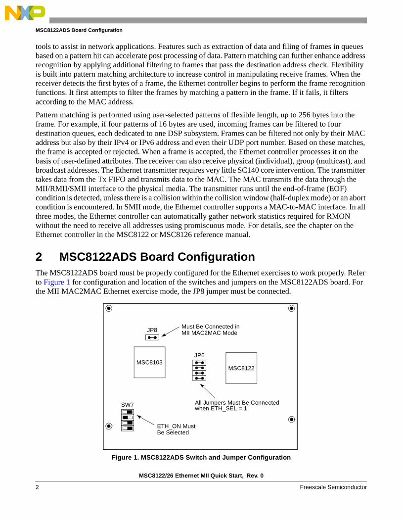
2 MSC8122ADS Board ConfigurationThe MSC8122ADS board must be properly configured for the Ethernet exercises to work properly. Refer to Figure 1 for configuration and location of the switches and jumpers on the MSC8122ADS board. For the MII MAC2MAC Ethernet exercise mode, the JP8 jumper must be connected.
Figure 1. MSC8122ADS Switch and Jumper Configuration
MSC8103MSC8122
JP8
JP6
SW7
Must Be Connected inMII MAC2MAC Mode
ETH_ON MustBe Selected
All Jumpers Must Be Connectedwhen ETH_SEL = 1
MSC8122/26 Ethernet MII Quick Start, Rev. 0
Freescale Semiconductor 3
MII MAC2MAC Exercise
3 MII MAC2MAC ExerciseWhen the MSC8122ADS board is properly set up, you can run the MSC8122 Ethernet exercise as follows:
1. Download and run the host (MSC8101/3) project.
2. Download and run the MSC8122 project.
3. Run the host project.
During the debug session, an STDIO window appears and displays the following message to indicate that the MSC8101/3 configuration of the MSC8122ADS board has successfully completed:
BCSR Init completed
4. Run the slave project.
Three messages indicate that the test ran, the Ethernet frame was successfully received, and the MAC2MAC exercise completed.
Welcome to ENET MII test - Core number 1MIIGSK_ENR=3Frame Was Received
MII mode requires the following preprocessor macros to be added in the project settings under the I/O and Preprocessors panel for both host and slave projects.
• DTEST_TYPE=MII_M2M_TP
• DTEST_SPEED=SPEED_100_MBPS
This exercise for both host and slave CodeWarrior™ projects is available in the AN3063SW zip file in the directory named MII_MAC2MAC_internal_loopback\projects\feth_all_tests_fulld_gpio_and_dsi.
3.1 MSC8103 Code (Host)The MSC8103 serves as a host to configure the board control and status registers (BCSRn). For this exercise, the MSC8103 host configures the BCSRn as shown in Table 1.
Table 1. BCSR Configuration for the MAC2MAC Exercise
Mode Port BCSR Configuration
MII MAC TO MAC GPIO Write(BCSR7, 0x07000000);NOP(100)Write(BCSR7, 0x15000000);Write(BCSR9, 0xC0000000)
MII MAC TO MAC DSI Write(BCSR7, 0x07000000);NOP(100)Write(BCSR7, 0x15000000);Write(BCSR9, 0xD0000000)

MSC8122/26 Ethernet MII Quick Start, Rev. 0
4 Freescale Semiconductor
MII MAC2MAC Exercise
3.2 MSC8122 Code (Slave)When the MSC8101/03 host is running, the MSC8122 code can run. The code starts with the variable and vector initialization. The following lines simply read and display the core ID, indicating the beginning of the MSC8122 Ethernet exercise.
Read(CIDR,&core_id);printf("Welcome to ENET MII test - Core number %d\n",core_id);
The following lines perform a soft reset on all MAC modules.
Write(MACCFG1, MACCFG1_SOFT_RESET);NOP(10000);Write(MACCFG1, 0x0);
The following function configures the MSC8122 PHY for the selected Ethernet operating mode. No configuration is necessary for the MAC2MAC mode described in this document.
configPhyForTest();
The transmit buffer descriptors are initialized for 1000 frames:
initTXBDs(NUM_OF_FRAMES);
The following function initializes the data patterns for use in transmitting the Ethernet frame.
initDataPatterns();
Following are the values to which the data patterns are initialized.
TYPE32BIT currDataAddress = FIRST_TX_DATA_ADDRESS;// DATA Buffer 0 // data: 0xFFFFFFFF
Write(currDataAddress,0x00000000);Write((currDataAddress+0x04),0x63640000);Write((currDataAddress+0x08),0x00006364);Write((currDataAddress+0x0C),0x002EFFFF);Write((currDataAddress+0x10),0xFFFFFFFF);Write((currDataAddress+0x14),0xFFFFFFFF);Write((currDataAddress+0x18),0xFFFFFFFF);Write((currDataAddress+0x1C),0xFFFFFFFF);Write((currDataAddress+0x20),0xFFFFFFFF);Write((currDataAddress+0x24),0xFFFFFFFF);Write((currDataAddress+0x28),0xFFFFFFFF);Write((currDataAddress+0x2C),0xFFFFFFFF);Write((currDataAddress+0x30),0xFFFFFFFF);Write((currDataAddress+0x34),0xFFFFFFFF);Write((currDataAddress+0x38),0xFFFFFFFF);
// DATA Buffer 1// data: 0xAAAAAAAAcurrDataAddress += 0x100;
Write(currDataAddress,0xF0FCDA00);Write((currDataAddress+0x04),0x42130000);Write((currDataAddress+0x08),0x00006364);Write((currDataAddress+0x0C),0x002EAAAA);Write((currDataAddress+0x10),0xAAAAAAAA);Write((currDataAddress+0x14),0xAAAAAAAA);

MSC8122/26 Ethernet MII Quick Start, Rev. 0
Freescale Semiconductor 5
MII MAC2MAC Exercise
Write((currDataAddress+0x18),0xAAAAAAAA);Write((currDataAddress+0x1C),0xAAAAAAAA);Write((currDataAddress+0x20),0xAAAAAAAA);Write((currDataAddress+0x24),0xAAAAAAAA);Write((currDataAddress+0x28),0xAAAAAAAA);Write((currDataAddress+0x2C),0xAAAAAAAA);Write((currDataAddress+0x30),0xAAAAAAAA);Write((currDataAddress+0x34),0xAAAAAAAA);Write((currDataAddress+0x38),0xAAAAAAAA);
// DATA Buffer 2// data: 0x55555555currDataAddress += 0x100;
Write(currDataAddress,0xF0FCDA00);Write((currDataAddress+0x04),0x42130000);Write((currDataAddress+0x08),0x00006364);Write((currDataAddress+0x0C),0x002E5555);Write((currDataAddress+0x10),0x55555555);Write((currDataAddress+0x14),0x55555555);Write((currDataAddress+0x18),0x55555555);Write((currDataAddress+0x1C),0x55555555);Write((currDataAddress+0x20),0x55555555);Write((currDataAddress+0x24),0x55555555);Write((currDataAddress+0x28),0x55555555);Write((currDataAddress+0x2C),0x55555555);Write((currDataAddress+0x30),0x55555555);Write((currDataAddress+0x34),0x55555555);Write((currDataAddress+0x38),0x55555555);
// DATA Buffer 3// data: 0x00000000currDataAddress += 0x100;
Write(currDataAddress,0xF0FCDA00);Write((currDataAddress+0x04),0x42130000);Write((currDataAddress+0x08),0x00006364);Write((currDataAddress+0x0C),0x002E0000);Write((currDataAddress+0x10),0x00000000);Write((currDataAddress+0x14),0x00000000);Write((currDataAddress+0x18),0x00000000);Write((currDataAddress+0x1C),0x00000000);Write((currDataAddress+0x20),0x00000000);Write((currDataAddress+0x24),0x00000000);Write((currDataAddress+0x28),0x00000000);Write((currDataAddress+0x2C),0x00000000);Write((currDataAddress+0x30),0x00000000);Write((currDataAddress+0x34),0x00000000);Write((currDataAddress+0x38),0x00000000);
Next, the receive buffer descriptors are initialized for the 1000 frames.
initRXBDs(NUM_OF_FRAMES);
The configEthernetRegisters() function is used to configure the MSC8122 Ethernet controller registers.
configEthernetRegisters();
Once the Ethernet Controller is configured the transmit buffer descriptors are enabled.
enableTXBDs(NUM_OF_FRAMES);
MSC8122/26 Ethernet MII Quick Start, Rev. 0
6 Freescale Semiconductor
MII MAC2MAC Exercise
Next, the MIIGSK[EN] bit is set, which enables the Ethernet controller to transmit/receive Ethernet frames.
Write(MIIGSK_ENR,0x1);NOP(100000);
The following code ensures that the Ethernet controller is ready for use. The MIIGSK_ENR[READY] bit is polled until the Ethernet controller is ready for use.
Read(MIIGSK_ENR,&ready);while(ready != 0x3){
NOP(10);Read(MIIGSK_ENR,&ready);printf("READY=%x\n",ready);
}printf("MIIGSK_ENR=%x\n",ready);
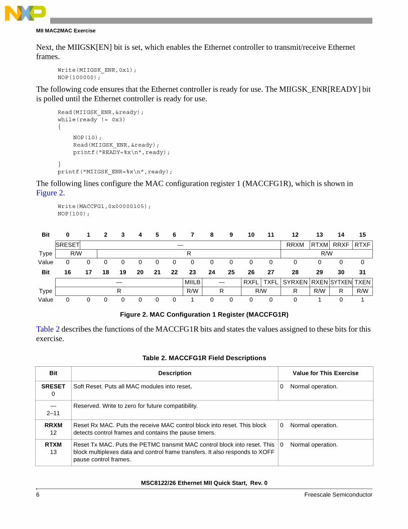
The following lines configure the MAC configuration register 1 (MACCFG1R), which is shown in Figure 2.
Write(MACCFG1,0x00000105);NOP(100);
Table 2 describes the functions of the MACCFG1R bits and states the values assigned to these bits for this exercise.
Bit 0 1 2 3 4 5 6 7 8 9 10 11 12 13 14 15
SRESET — RRXM RTXM RRXF RTXF
Type R/W R R/W
Value 0 0 0 0 0 0 0 0 0 0 0 0 0 0 0 0
Bit 16 17 18 19 20 21 22 23 24 25 26 27 28 29 30 31
— MIILB — RXFL TXFL SYRXEN RXEN SYTXEN TXEN
Type R R/W R R/W R R/W R R/W
Value 0 0 0 0 0 0 0 1 0 0 0 0 0 1 0 1
Figure 2. MAC Configuration 1 Register (MACCFG1R)
Table 2. MACCFG1R Field Descriptions
Bit Description Value for This Exercise
SRESET0
Soft Reset. Puts all MAC modules into reset. 0 Normal operation.
—2–11
Reserved. Write to zero for future compatibility.
RRXM12
Reset Rx MAC. Puts the receive MAC control block into reset. This block detects control frames and contains the pause timers.
0 Normal operation.
RTXM13
Reset Tx MAC. Puts the PETMC transmit MAC control block into reset. This block multiplexes data and control frame transfers. It also responds to XOFF pause control frames.
0 Normal operation.

MSC8122/26 Ethernet MII Quick Start, Rev. 0
Freescale Semiconductor 7
MII MAC2MAC Exercise
The following polling code detects when the frame transmission is complete.
Write(0x02001000,0xdc00003c);Read(0x02009000,&ready);while(ready!=0x0c000040){Read(0x02009000,&ready);}
The following lines execute when the frame is received, and code execution stops at the debug statement.
printf("Frame Was Received\n");asm(" debug");
3.3 Ethernet_Setup()The Ethernet_Setup() function is used to configure the Ethernet controller registers. This section describes the process of using this function to configure the following registers in the order listed:
1. MIIGSK Configuration Register (MIIGSK_CFGR) to set up certain overall modes and features of the Ethernet controller.
2. MIIGSK Enable Register (MIIGSK_ENR) to enable Ethernet operation.
RRXF14
Reset Rx Function. Puts the receive function block into reset. This block performs the receive frame protocol.
0 Normal operation.
RTXF15
Reset Tx Function. Puts the transmit function block into reset. This block performs the frame transmission protocol.
0 Normal operation.
—16–22
Reserved. Write to zero for future compatibility.
MIILB23
MII Loopback. Causes the MII MAC transmit outputs to be looped back to the MAC receive inputs.
1 MII Loopback mode.
—24–25
Reserved. Write to zero for future compatibility.
RXFL26
Rx Flow. Causes the receive MAC control to detect and act on pause flow control frames.
0 Ignore receive pause flow control frames.
TXFL27
Tx Flow. Allows the transmit MAC control to send pause flow control frames if the system requests them. Clearing this bit prevents the transmit MAC control from sending flow control frames.
0 No transmit pause flow control frames.
SYRXEN28
Synchronized Rx Enable. Receive enable synchronized to the receive stream.
0 Frame reception is not enabled.
RXEN29
Receive Enable. Allows the MAC to receive frames from the PHY. Clearing this bit prevents the reception of frames.
1 MAC can receive frames.
SYTXEN30
Synchronized TX Enable. Transmit Enable synchronized to the transmit stream.
0 Frame transmission is not enabled.
TXEN31
Transmit Enable. Allows the MAC to transmit frames from the system. Clearing this bit prevents the transmission of frames.
1 MAC can transmit frames.
Table 2. MACCFG1R Field Descriptions (continued)
Bit Description Value for This Exercise

MSC8122/26 Ethernet MII Quick Start, Rev. 0
8 Freescale Semiconductor
MII MAC2MAC Exercise
3. MAC configuration 2 register (MACCFG2R), which is the second of two user-programmable registers to configure MAC functionality.
4. MAC station address registers, MACSTADDR1R and MACSTNADDR2R. These two user-programmable registers hold the physical address that the Ethernet controller compares with the destination address field of the received frame.
5. Interrupt Event Register (IEVENT) to set up and specify interrupt events.
6. Interrupt Mask Register (IMASK) to enable the events specified in IEVENT.
7. Group Address Registers 0–7 (GADDR[0–7]) and Individual Address Registers 0–7 (IADDR[0–7]) for hash functionality.
8. A set of pattern matching control and attribute registers.
9. Maximum receive buffer length R0R1 Register (MRBLR0R1) to define the maximum number of bytes that can be written to a receive buffer descriptor ring before moving to the next buffer.
10. DMA maintenance and control registers and an Ethernet control register.
For MAC-to-MAC operation, the following registers are configured:
Write(MIIGSK_CFGR, 0x00000000);stIPBus1Regs->stEnet.vuliMIIMCFGR = 0x00000000;
MIIGSK_CFGR is a user-programmable register with configuration bits for different modes and features of the MSC8122 Ethernet controller. For this example, this register is configured as shown in Figure 3.
Table 3 describes the functions of the MIIGSK_CFGR bits and states the values assigned to these bits for this exercise.
Bit 0 1 2 3 4 5 6 7 8 9 10 11 12 13 14 15
—
Type R
Value 0 0 0 0 0 0 0 0 0 0 0 0 0 0 0 0
Bit 16 17 18 19 20 21 22 23 24 25 26 27 28 29 30 31
— FRCONT — LBMODE EMODE — IFMODE
Type R R/W R R/W R R/W
Value 0 0 0 0 0 0 0 0 0 0 0 0 0 0 0 0
Figure 3. MIIGSK Configuration Register (MIIGSK_CFGR)
Table 3. MIIGSK_CFGR Bit Descriptions
Bit Description Values for This Exercise
—0–24
Reserved.
FRCONT25
Frequency Control. Determines the frequency of the clock source to the Ethernet controller to support 10/100 Mbps operations in RMII/SMII modes of operation. (In SMII mode, ETHCLOCK, and in RMII mode, ETHREF_CLK.). This field has no effect in MII mode.
0 In RMII mode, the clock source (ETHREF_CLK) is 50 MHz to support 100 Mbps operation. In SMII mode, the clock source (ETHCLOCK) is 125 MHz to support 100 Mbps operation.

MSC8122/26 Ethernet MII Quick Start, Rev. 0
Freescale Semiconductor 9
MII MAC2MAC Exercise
When MIIGSK_CFGR is configured, the Ethernet controller must be enabled for operation, as follows:
Write(MIIGSK_ENR,0x1);
The MIIGSK_ENR register enables or disables Ethernet controller operation and indicates when the Ethernet controller is ready for use. For this example, this register is configured as shown in Figure 4.
Table 4 describes the functions of the MIIGSK_ENR bits and states the values assigned to these bits for this exercise.
—26
Reserved.
LBMODE27
RMII/SMII Sync Out - Internal Loopback Mode. Causes the Ethernet controller RMII/SMII transmit outputs to be looped back to the Ethernet controller RMII/SMII receive inputs.
0 Normal operation.
EMODE28
Echo Mode. Causes the Ethernet controller MII receive inputs from the MII PHY to be looped back to the Ethernet controller transmit outputs to the MII PHY.
0 Normal operation (the default).
—29
Reserved.
IFMODE30–31
Interface Mode. Specifies the type of interface to which the Ethernet controller is connected.
00 MII mode.
Bit 0 1 2 3 4 5 6 7 8 9 10 11 12 13 14 15
—
Type R
Value 0 0 0 0 0 0 0 0 0 0 0 0 0 0 0 0
Bit 16 17 18 19 20 21 22 23 24 25 26 27 28 29 30 31
— READY EN
Type R R/W
Value 0 0 0 0 0 0 0 0 0 0 0 0 0 0 1 1
Figure 4. MIIGSK Enable Register (MIIGSK_ENR)
Table 4. MIIGSK_ENR Bit Descriptions
Bit Description Values for this Exercise
—0–29
Reserved.
READY30
Ready. This bit is set when the Ethernet controller is ready for use. This bit is read-only.
EN31
Enable. Enables/disables Ethernet controller operation. 1 The Ethernet controller can transmit/receive frames.
Table 3. MIIGSK_CFGR Bit Descriptions (continued)
Bit Description Values for This Exercise
MSC8122/26 Ethernet MII Quick Start, Rev. 0
10 Freescale Semiconductor
MII MAC2MAC Exercise
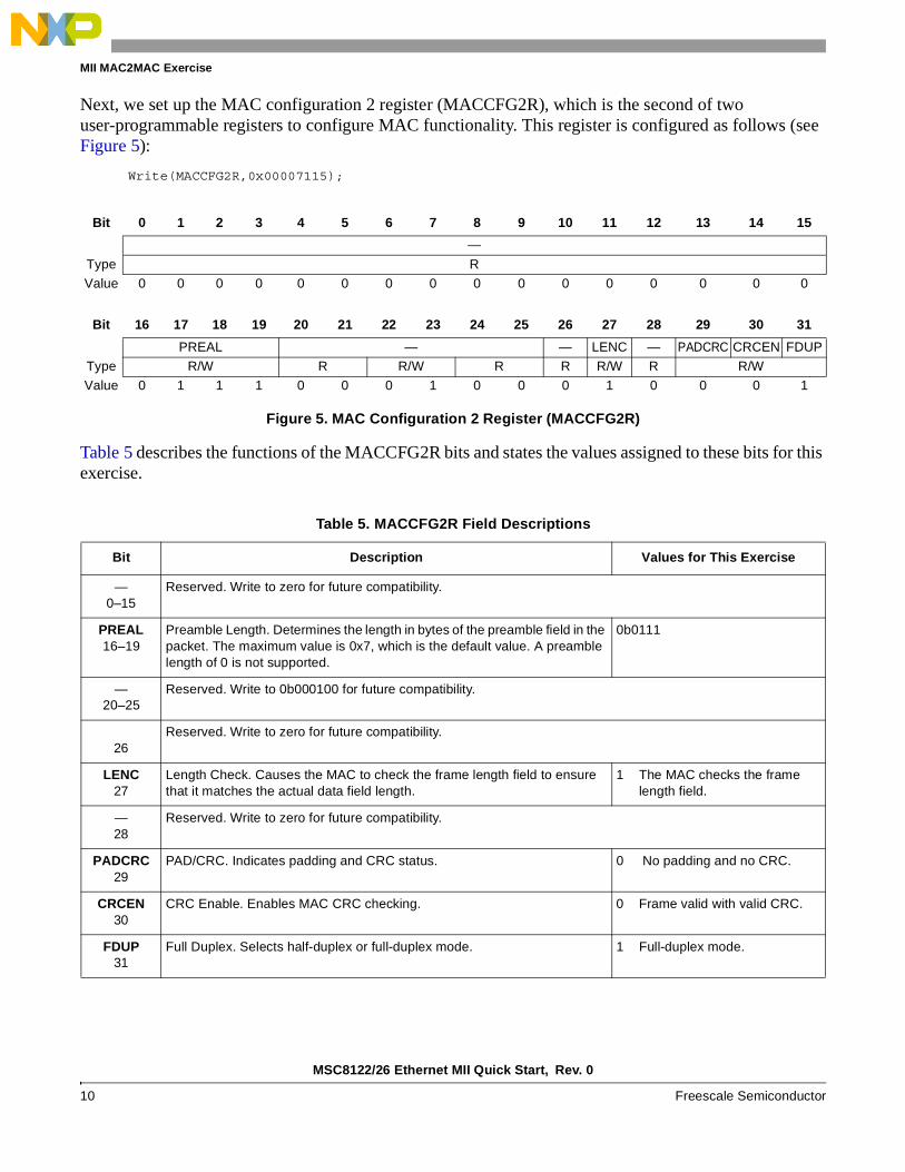
Next, we set up the MAC configuration 2 register (MACCFG2R), which is the second of two user-programmable registers to configure MAC functionality. This register is configured as follows (see Figure 5):
Write(MACCFG2R,0x00007115);
Bit 0 1 2 3 4 5 6 7 8 9 10 11 12 13 14 15
—
Type R
Value 0 0 0 0 0 0 0 0 0 0 0 0 0 0 0 0
Bit 16 17 18 19 20 21 22 23 24 25 26 27 28 29 30 31
PREAL — — LENC — PADCRC CRCEN FDUP
Type R/W R R/W R R R/W R R/W
Value 0 1 1 1 0 0 0 1 0 0 0 1 0 0 0 1
Figure 5. MAC Configuration 2 Register (MACCFG2R)
Table 5 describes the functions of the MACCFG2R bits and states the values assigned to these bits for this exercise.
Table 5. MACCFG2R Field Descriptions
Bit Description Values for This Exercise
—0–15
Reserved. Write to zero for future compatibility.
PREAL16–19
Preamble Length. Determines the length in bytes of the preamble field in the packet. The maximum value is 0x7, which is the default value. A preamble length of 0 is not supported.
0b0111
—20–25
Reserved. Write to 0b000100 for future compatibility.
26Reserved. Write to zero for future compatibility.
LENC27
Length Check. Causes the MAC to check the frame length field to ensure that it matches the actual data field length.
1 The MAC checks the frame length field.
—28
Reserved. Write to zero for future compatibility.
PADCRC29
PAD/CRC. Indicates padding and CRC status. 0 No padding and no CRC.
CRCEN30
CRC Enable. Enables MAC CRC checking. 0 Frame valid with valid CRC.
FDUP31
Full Duplex. Selects half-duplex or full-duplex mode. 1 Full-duplex mode.
MSC8122/26 Ethernet MII Quick Start, Rev. 0
Freescale Semiconductor 11
MII MAC2MAC Exercise
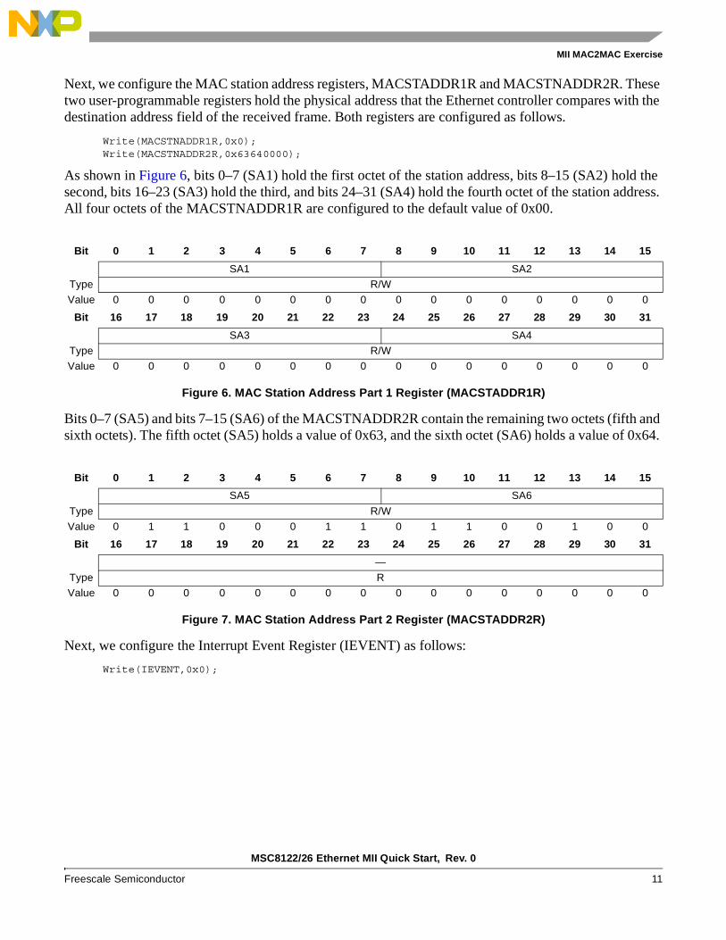
Next, we configure the MAC station address registers, MACSTADDR1R and MACSTNADDR2R. These two user-programmable registers hold the physical address that the Ethernet controller compares with the destination address field of the received frame. Both registers are configured as follows.
Write(MACSTNADDR1R,0x0);Write(MACSTNADDR2R,0x63640000);
As shown in Figure 6, bits 0–7 (SA1) hold the first octet of the station address, bits 8–15 (SA2) hold the second, bits 16–23 (SA3) hold the third, and bits 24–31 (SA4) hold the fourth octet of the station address. All four octets of the MACSTNADDR1R are configured to the default value of 0x00.
Bits 0–7 (SA5) and bits 7–15 (SA6) of the MACSTNADDR2R contain the remaining two octets (fifth and sixth octets). The fifth octet (SA5) holds a value of 0x63, and the sixth octet (SA6) holds a value of 0x64.
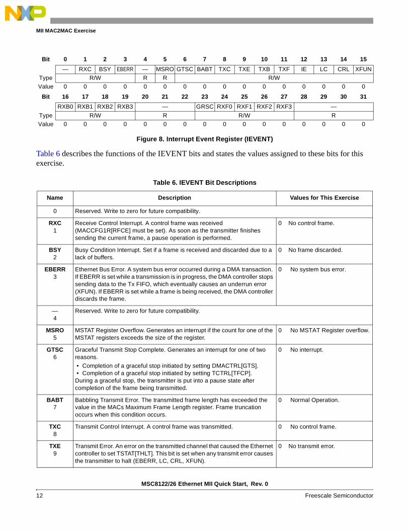
Next, we configure the Interrupt Event Register (IEVENT) as follows:
Write(IEVENT,0x0);
Bit 0 1 2 3 4 5 6 7 8 9 10 11 12 13 14 15
SA1 SA2
Type R/W
Value 0 0 0 0 0 0 0 0 0 0 0 0 0 0 0 0
Bit 16 17 18 19 20 21 22 23 24 25 26 27 28 29 30 31
SA3 SA4
Type R/W
Value 0 0 0 0 0 0 0 0 0 0 0 0 0 0 0 0
Figure 6. MAC Station Address Part 1 Register (MACSTADDR1R)
Bit 0 1 2 3 4 5 6 7 8 9 10 11 12 13 14 15
SA5 SA6
Type R/W
Value 0 1 1 0 0 0 1 1 0 1 1 0 0 1 0 0
Bit 16 17 18 19 20 21 22 23 24 25 26 27 28 29 30 31
—
Type R
Value 0 0 0 0 0 0 0 0 0 0 0 0 0 0 0 0
Figure 7. MAC Station Address Part 2 Register (MACSTADDR2R)
MSC8122/26 Ethernet MII Quick Start, Rev. 0
12 Freescale Semiconductor
MII MAC2MAC Exercise
Table 6 describes the functions of the IEVENT bits and states the values assigned to these bits for this exercise.
Bit 0 1 2 3 4 5 6 7 8 9 10 11 12 13 14 15
— RXC BSY EBERR — MSRO GTSC BABT TXC TXE TXB TXF IE LC CRL XFUN
Type R/W R R R/W
Value 0 0 0 0 0 0 0 0 0 0 0 0 0 0 0 0
Bit 16 17 18 19 20 21 22 23 24 25 26 27 28 29 30 31
RXB0 RXB1 RXB2 RXB3 — GRSC RXF0 RXF1 RXF2 RXF3 —
Type R/W R R/W R
Value 0 0 0 0 0 0 0 0 0 0 0 0 0 0 0 0
Figure 8. Interrupt Event Register (IEVENT)
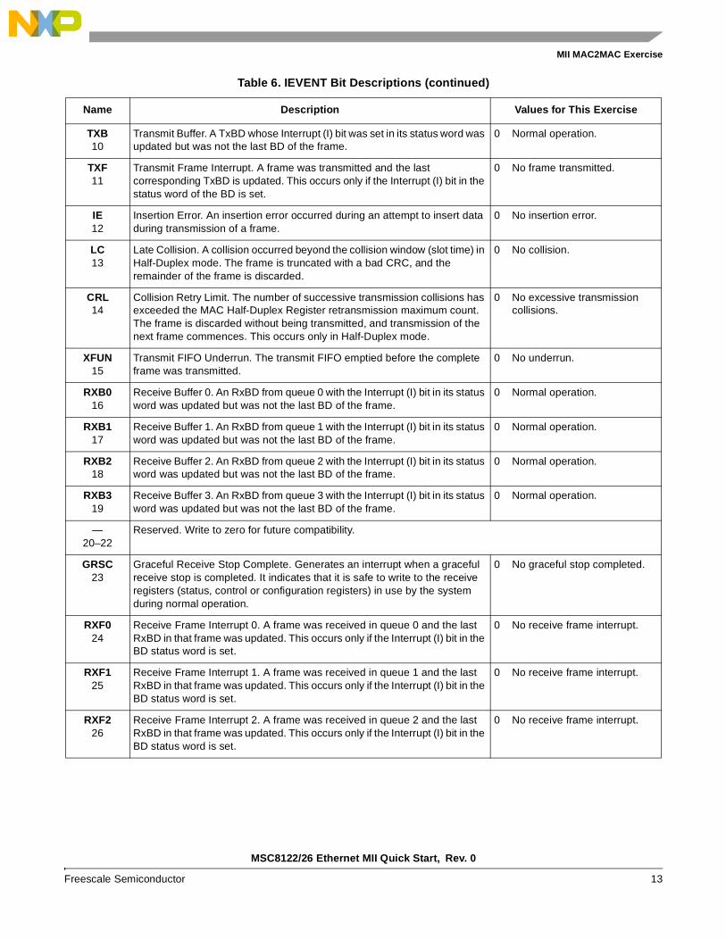
Table 6. IEVENT Bit Descriptions
Name Description Values for This Exercise
0 Reserved. Write to zero for future compatibility.
RXC1
Receive Control Interrupt. A control frame was received (MACCFG1R[RFCE] must be set). As soon as the transmitter finishes sending the current frame, a pause operation is performed.
0 No control frame.
BSY2
Busy Condition Interrupt. Set if a frame is received and discarded due to a lack of buffers.
0 No frame discarded.
EBERR3
Ethernet Bus Error. A system bus error occurred during a DMA transaction. If EBERR is set while a transmission is in progress, the DMA controller stops sending data to the Tx FIFO, which eventually causes an underrun error (XFUN). If EBERR is set while a frame is being received, the DMA controller discards the frame.
0 No system bus error.
—4
Reserved. Write to zero for future compatibility.
MSRO5
MSTAT Register Overflow. Generates an interrupt if the count for one of the MSTAT registers exceeds the size of the register.
0 No MSTAT Register overflow.
GTSC6
Graceful Transmit Stop Complete. Generates an interrupt for one of two reasons.
• Completion of a graceful stop initiated by setting DMACTRL[GTS]. • Completion of a graceful stop initiated by setting TCTRL[TFCP].During a graceful stop, the transmitter is put into a pause state after completion of the frame being transmitted.
0 No interrupt.
BABT7
Babbling Transmit Error. The transmitted frame length has exceeded the value in the MACs Maximum Frame Length register. Frame truncation occurs when this condition occurs.
0 Normal Operation.
TXC8
Transmit Control Interrupt. A control frame was transmitted. 0 No control frame.
TXE9
Transmit Error. An error on the transmitted channel that caused the Ethernet controller to set TSTAT[THLT]. This bit is set when any transmit error causes the transmitter to halt (EBERR, LC, CRL, XFUN).
0 No transmit error.
MSC8122/26 Ethernet MII Quick Start, Rev. 0
Freescale Semiconductor 13
MII MAC2MAC Exercise
TXB10
Transmit Buffer. A TxBD whose Interrupt (I) bit was set in its status word was updated but was not the last BD of the frame.
0 Normal operation.
TXF11
Transmit Frame Interrupt. A frame was transmitted and the last corresponding TxBD is updated. This occurs only if the Interrupt (I) bit in the status word of the BD is set.
0 No frame transmitted.
IE12
Insertion Error. An insertion error occurred during an attempt to insert data during transmission of a frame.
0 No insertion error.
LC13
Late Collision. A collision occurred beyond the collision window (slot time) in Half-Duplex mode. The frame is truncated with a bad CRC, and the remainder of the frame is discarded.
0 No collision.
CRL14
Collision Retry Limit. The number of successive transmission collisions has exceeded the MAC Half-Duplex Register retransmission maximum count. The frame is discarded without being transmitted, and transmission of the next frame commences. This occurs only in Half-Duplex mode.
0 No excessive transmission collisions.
XFUN15
Transmit FIFO Underrun. The transmit FIFO emptied before the complete frame was transmitted.
0 No underrun.
RXB016
Receive Buffer 0. An RxBD from queue 0 with the Interrupt (I) bit in its status word was updated but was not the last BD of the frame.
0 Normal operation.
RXB117
Receive Buffer 1. An RxBD from queue 1 with the Interrupt (I) bit in its status word was updated but was not the last BD of the frame.
0 Normal operation.
RXB218
Receive Buffer 2. An RxBD from queue 2 with the Interrupt (I) bit in its status word was updated but was not the last BD of the frame.
0 Normal operation.
RXB319
Receive Buffer 3. An RxBD from queue 3 with the Interrupt (I) bit in its status word was updated but was not the last BD of the frame.
0 Normal operation.
—20–22
Reserved. Write to zero for future compatibility.
GRSC23
Graceful Receive Stop Complete. Generates an interrupt when a graceful receive stop is completed. It indicates that it is safe to write to the receive registers (status, control or configuration registers) in use by the system during normal operation.
0 No graceful stop completed.
RXF024
Receive Frame Interrupt 0. A frame was received in queue 0 and the last RxBD in that frame was updated. This occurs only if the Interrupt (I) bit in the BD status word is set.
0 No receive frame interrupt.
RXF125
Receive Frame Interrupt 1. A frame was received in queue 1 and the last RxBD in that frame was updated. This occurs only if the Interrupt (I) bit in the BD status word is set.
0 No receive frame interrupt.
RXF226
Receive Frame Interrupt 2. A frame was received in queue 2 and the last RxBD in that frame was updated. This occurs only if the Interrupt (I) bit in the BD status word is set.
0 No receive frame interrupt.
Table 6. IEVENT Bit Descriptions (continued)
Name Description Values for This Exercise
MSC8122/26 Ethernet MII Quick Start, Rev. 0
14 Freescale Semiconductor
MII MAC2MAC Exercise
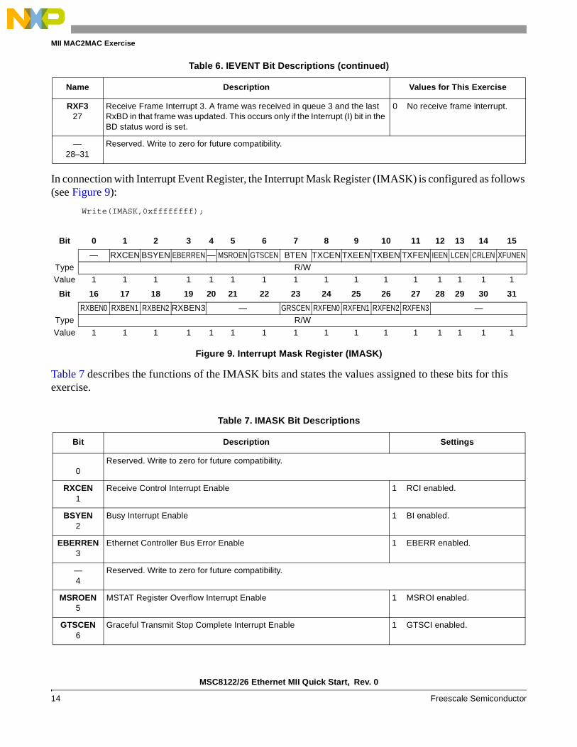
In connection with Interrupt Event Register, the Interrupt Mask Register (IMASK) is configured as follows (see Figure 9):
Write(IMASK,0xffffffff);
Table 7 describes the functions of the IMASK bits and states the values assigned to these bits for this exercise.
RXF327
Receive Frame Interrupt 3. A frame was received in queue 3 and the last RxBD in that frame was updated. This occurs only if the Interrupt (I) bit in the BD status word is set.
0 No receive frame interrupt.
—28–31
Reserved. Write to zero for future compatibility.
Bit 0 1 2 3 4 5 6 7 8 9 10 11 12 13 14 15
— RXCEN BSYEN EBERREN — MSROEN GTSCEN BTEN TXCEN TXEEN TXBEN TXFEN IEEN LCEN CRLEN XFUNEN
Type R/W
Value 1 1 1 1 1 1 1 1 1 1 1 1 1 1 1 1
Bit 16 17 18 19 20 21 22 23 24 25 26 27 28 29 30 31
RXBEN0 RXBEN1 RXBEN2 RXBEN3 — GRSCEN RXFEN0 RXFEN1 RXFEN2 RXFEN3 —
Type R/W
Value 1 1 1 1 1 1 1 1 1 1 1 1 1 1 1 1
Figure 9. Interrupt Mask Register (IMASK)
Table 7. IMASK Bit Descriptions
Bit Description Settings
0Reserved. Write to zero for future compatibility.
RXCEN1
Receive Control Interrupt Enable 1 RCI enabled.
BSYEN2
Busy Interrupt Enable 1 BI enabled.
EBERREN3
Ethernet Controller Bus Error Enable 1 EBERR enabled.
—4
Reserved. Write to zero for future compatibility.
MSROEN5
MSTAT Register Overflow Interrupt Enable 1 MSROI enabled.
GTSCEN6
Graceful Transmit Stop Complete Interrupt Enable 1 GTSCI enabled.
Table 6. IEVENT Bit Descriptions (continued)
Name Description Values for This Exercise

MSC8122/26 Ethernet MII Quick Start, Rev. 0
Freescale Semiconductor 15
MII MAC2MAC Exercise
BTEN7
Babbling Transmitter Interrupt Enable 1 BTI enabled.
TXCEN8
Transmit Control Interrupt Enable 1 TCI enabled.
TXEEN9
Transmit Error Interrupt Enable 1 TEI enabled.
TXBEN10
Transmit Buffer Interrupt Enable 1 TBI enabled.
TXFEN11
Transmit Frame Interrupt Enable 1 TFI enabled.
IEEN12
Insertion Error Interrupt Enable 1 IEI enabled.
LCEN13
Late Collision Enable 1 LC enabled.
CRLEN14
Collision Retry Limit Enable 1 CRL enabled.
XFUNEN15
Transmit FIFO Underrun Enable 1 TFU enabled.
RXBEN016
Receive Buffer Queue 0 Interrupt Enable 1 RBQ0I enabled.
RXBEN117
Receive Buffer Queue 1 Interrupt Enable 1 RBQ1I enabled.
RXBEN218
Receive Buffer Queue 2 Interrupt Enable 1 RBQ2I enabled.
RXBEN319
Receive Buffer Queue 3 Interrupt Enable 1 RBQ3I enabled.
—20–22
Reserved. Write to zero for future compatibility.
GRSCEN23
Graceful Receive Stop Complete Interrupt Enable 1 GRSCI enabled.
RXFEN024
Receive Frame Queue 0 Interrupt Enable 1 RFQ0I enabled.
RXFEN125
Receive Frame Queue 1 Interrupt Enable 1 RFQ1I enabled.
RXFEN226
Receive Frame Queue 2 Interrupt Enable 1 RFQ2I enabled.
RXFEN327
Receive Frame Queue 3 Interrupt Enable 1 RFQ3I enabled.
—28–31
Reserved. Write to zero for future compatibility.
Table 7. IMASK Bit Descriptions (continued)
Bit Description Settings
MSC8122/26 Ethernet MII Quick Start, Rev. 0
16 Freescale Semiconductor
MII MAC2MAC Exercise
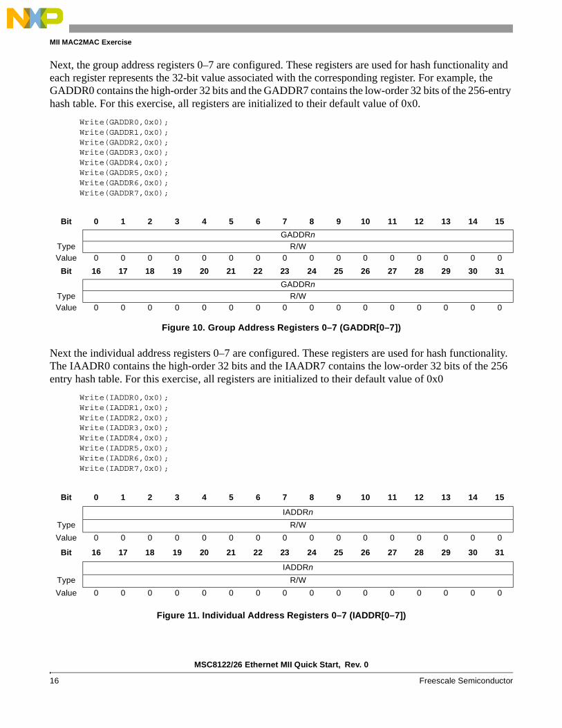
Next, the group address registers 0–7 are configured. These registers are used for hash functionality and each register represents the 32-bit value associated with the corresponding register. For example, the GADDR0 contains the high-order 32 bits and the GADDR7 contains the low-order 32 bits of the 256-entry hash table. For this exercise, all registers are initialized to their default value of 0x0.
Write(GADDR0,0x0);Write(GADDR1,0x0);Write(GADDR2,0x0);Write(GADDR3,0x0);Write(GADDR4,0x0);Write(GADDR5,0x0);Write(GADDR6,0x0);Write(GADDR7,0x0);
Next the individual address registers 0–7 are configured. These registers are used for hash functionality. The IAADR0 contains the high-order 32 bits and the IAADR7 contains the low-order 32 bits of the 256 entry hash table. For this exercise, all registers are initialized to their default value of 0x0
Write(IADDR0,0x0);Write(IADDR1,0x0);Write(IADDR2,0x0);Write(IADDR3,0x0);Write(IADDR4,0x0);Write(IADDR5,0x0);Write(IADDR6,0x0);Write(IADDR7,0x0);
Bit 0 1 2 3 4 5 6 7 8 9 10 11 12 13 14 15
GADDRnType R/WValue 0 0 0 0 0 0 0 0 0 0 0 0 0 0 0 0
Bit 16 17 18 19 20 21 22 23 24 25 26 27 28 29 30 31
GADDRnType R/WValue 0 0 0 0 0 0 0 0 0 0 0 0 0 0 0 0
Figure 10. Group Address Registers 0–7 (GADDR[0–7])
Bit 0 1 2 3 4 5 6 7 8 9 10 11 12 13 14 15
IADDRn
Type R/W
Value 0 0 0 0 0 0 0 0 0 0 0 0 0 0 0 0
Bit 16 17 18 19 20 21 22 23 24 25 26 27 28 29 30 31
IADDRn
Type R/W
Value 0 0 0 0 0 0 0 0 0 0 0 0 0 0 0 0
Figure 11. Individual Address Registers 0–7 (IADDR[0–7])

MSC8122/26 Ethernet MII Quick Start, Rev. 0
Freescale Semiconductor 17
MII MAC2MAC Exercise
Next the pattern matching registers are configured. These user-programmable registers contain 32-bit data used to compare against the data of the received frames. There are sixteen pattern matching registers for detecting the same number of different 32-bit data patterns. The PMDn, PMASKn, PCNTRLn, and PATTRBn registers are used in conjunction to configure pattern matching functionality.
First the pattern matching data register 0 (PMD0) is configured with the value of 0x0, which represents the 32 bits of data to compare against the frame data.
Write(PMD0,0x00000000);
Next the pattern mask data register 0 (PMASK0) is configured, as follows:
Write(PMASK0,0xffffffff);
The pattern mask register specifies the 32-bit mask for pattern matching. In this example, all bits are unmasked to enable corresponding PDMn bits for pattern match compares. If a bit is masked, it is considered a match. When the data bit is unmasked, the corresponding PMDn bit is enabled for pattern match compares (with frame data).
Next pattern match control register 0 (PCNTRL0) is configured as follows (see Figure 12):
Write(PCNTRL0,0x000000c2);
Table 8 describes the functions of the PCNTRL0 bits and states the values assigned to these bits for this exercise.
Bit 0 1 2 3 4 5 6 7 8 9 10 11 12 13 14 15
—
Type R
Reset 0 0 0 0 0 0 0 0 0 0 0 0 0 0 0 0
Bit 16 17 18 19 20 21 22 23 24 25 26 27 28 29 30 31
— MI CSE CP — PMC
Type R R/W R
Reset 0 0 0 0 0 0 0 0 1 1 0 0 0 0 1 0
Figure 12. Pattern Match Control Register 0 (PCNTRL0)
Table 8. PCNTRL0 Bit Descriptions
Bits Description Values for This Exercise
0–17 Reserved. Write to zero for future compatibility.
MI18–23
Matching Index. Specifies the index, in multiples of 4 bytes, from the start of the receive frame (from the DA field to FCS inclusive) to perform the pattern matching. For example, MI as cleared corresponds to the first 4-bytes of the destination address. The maximum programmed value for MI is 63 (252-byte offset). The MI value for each 4-byte pattern is always honored (regardless of PCNTRLn[CP]), allowing for contiguous or non-contiguous patterns.
0b000000

MSC8122/26 Ethernet MII Quick Start, Rev. 0
18 Freescale Semiconductor
MII MAC2MAC Exercise
Next pattern match attribute register 0 (PATTRB0) is configured as follows (see Figure 13):
Write(PATTRB0,0x00000200);
Table 9 describes the functions of the PATTRB0 bits and states the values assigned to these bits for this exercise.
CSE24
Continue Search Enable. Indicates that if a match occurs on an entry in which the CSE bit is set, the pattern matching should continue. If no other matches are encountered, the attributes corresponding to the last matched entry are used. If a pattern match reject occurs, CSE is ignored (the frame is rejected and searching is discontinued).
1 If the pattern matched, continue searching for other patterns up unto the 256-byte maximum.
CP25
Concatenated Pattern. The immediate pattern registers that follow are regarded as a continuation of this pattern. For example, PCNTRL0[CP] as set means pattern 0 and pattern 1 are joined together as one pattern. CP as set is always honored and PCNTRL15[CP] is always regarded as cleared, regardless. The lowest numerical PCNTRLn register in which CP is set contains the pattern matching control and attribute information (except MI) that is used for concatenated patterns. For each concatenated pattern, the MI field must be set to the appropriate 4-byte multiple. Otherwise, all the patterns attempt to match to the first 4-bytes of the DA (if MI is left cleared).
1 The immediate pattern that follows is concatenated to the current one.
—26–29
Reserved. Write to zero for future compatibility.
PMC30–31
Pattern Match Control. Controls the filtering of frames based on pattern matching.
10 Pattern Match Accept. The frame is accepted (subject to the CSE bit).
Bit 0 1 2 3 4 5 6 7 8 9 10 11 12 13 14 15
—
Type R
Value 0 0 0 0 0 0 0 0 0 0 0 0 0 0 0 0
Bit 16 17 18 19 20 21 22 23 24 25 26 27 28 29 30 31
— PMF — RDSEN RBDSEN — QC
Type R R/W R R/W R/W R R/W
Value 0 0 0 0 0 0 1 0 0 0 0 0 0 0 0 0
Figure 13. Pattern Match Attributes Register 0 (PATTRB0)
Table 9. PATTRB0 Field Descriptions
Bits Description Values for This Exercise
—0–21
Reserved. Write to zero for future compatibility.
PMF22
Pattern Match File. Specifies which field is used to determine where the frame is filled.
1 If a match occurs, the PATTRB[QC] field is used to determine where the frame is filed.
Table 8. PCNTRL0 Bit Descriptions (continued)
Bits Description Values for This Exercise

MSC8122/26 Ethernet MII Quick Start, Rev. 0
Freescale Semiconductor 19
MII MAC2MAC Exercise
Similarly, the pattern matching registers are configured for the second register set. Pattern matching data register 1 (PMD1) is configured as follows:
Write(PMD1,0x63640000);
Next, the pattern mask data register 1 (PMASK1) is configured as follows:
Write(PMASK1,0xffff0000);
Next, pattern match control register 1 (PCNTRL1) is configured as follows:
Write(PCNTRL1,0x00000102);
Table 11 describes the functions of the PCNTRL1 bits and states the values assigned to these bits for this exercise.
—23
Reserved. Write to zero for future compatibility.
RDSEN24
Rx Data Snoop Enable. Enables/disables snooping of all receive frame data to memory.
0 Disables snooping of all receive frame data to memory.
RBDSEN25
RxBD Snoop Enable. Enables/disables snooping of all RxBD memory accesses.
0 Disables snooping of all receive BD memory accesses.
—26–29
Reserved. Write to zero for future compatibility.
QC30–31
Queue Classification. Specifies the receive queue classification in which to file an incoming frame if the PATTRBn[PMF] field is set and a corresponding pattern match occurs. In the case of concatenated pattern configurations the QC used is from the first 4-byte pattern.
00 0 queue.
Bit 0 1 2 3 4 5 6 7 8 9 10 11 12 13 14 15
—
Type R
Value 0 0 0 0 0 0 0 0 0 0 0 0 0 0 0 0
Bit 16 17 18 19 20 21 22 23 24 25 26 27 28 29 30 31
— MI CSE CP — PMC
Type R R/W R
Value 0 0 0 0 0 0 0 1 0 0 0 0 0 0 1 0
Table 10. Pattern Match Control Register 1 (PCNTRL1)
Table 9. PATTRB0 Field Descriptions (continued)
Bits Description Values for This Exercise

MSC8122/26 Ethernet MII Quick Start, Rev. 0
20 Freescale Semiconductor
MII MAC2MAC Exercise
Next, pattern match attribute register 1 is configured as follows (see Figure 14):
Write(PATTRB1,0x00000200);
Table 12 describes the functions of the PATTRB1 bits and states the values assigned to these bits for this exercise.
Table 11. PCNTRL1 Bit Descriptions
Bits Description Values for This Exercise
0–17 Reserved. Write to zero for future compatibility.
MI18–23
Matching Index. Specifies the index, in multiples of 4 bytes, from the start of the receive frame (from the DA field to FCS inclusive) to perform the pattern matching. For example, MI as cleared corresponds to the first 4-bytes of the destination address. The maximum programmed value for MI is 63 (252-byte offset). The MI value for each 4-byte pattern is always honored (regardless of PCNTRLn[CP]), allowing for contiguous or non-contiguous patterns.
000001
CSE24
Continue Search Enable. Indicates that if a match occurs on an entry in which the CSE bit is set, the pattern matching should continue. If no other matches are encountered, the attributes corresponding to the last matched entry are used. If a pattern match reject occurs, CSE is ignored (the frame is rejected and searching is discontinued).
0 If the pattern matched, discontinue the search for all other patterns.
CP25
Concatenated Pattern. The immediate pattern registers that follow are regarded as a continuation of this pattern. For example, PCNTRL0[CP] as set means pattern 0 and pattern 1 are joined together as one pattern. CP as set is always honored and PCNTRL15[CP] is always regarded as cleared, regardless. The lowest numerical PCNTRLn register in which CP is set contains the pattern matching control and attribute information (except MI) that is used for concatenated patterns. For each concatenated pattern, the MI field must be set to the appropriate 4-byte multiple. Otherwise, all the patterns attempt to match to the first 4-bytes of the DA (if MI is left cleared).
0 No pattern concatenation with the following pattern is performed.
—26–29
Reserved. Write to zero for future compatibility.
PMC30–31
Pattern Match Control. Controls the filtering of frames based on pattern matching.
10 Pattern Match Accept. The frame is accepted (subject to the CSE bit).
Bit 0 1 2 3 4 5 6 7 8 9 10 11 12 13 14 15
—
Type R
Value 0 0 0 0 0 0 0 0 0 0 0 0 0 0 0 0
Bit 16 17 18 19 20 21 22 23 24 25 26 27 28 29 30 31
— PMF — RDSEN RBDSEN — QC
Type R R/W R R/W R/W R R/W
Value 0 0 0 0 0 0 1 0 0 0 0 0 0 0 0 0
Figure 14. Pattern Match Attributes Register 1 (PATTRB1)
MSC8122/26 Ethernet MII Quick Start, Rev. 0
Freescale Semiconductor 21
MII MAC2MAC Exercise
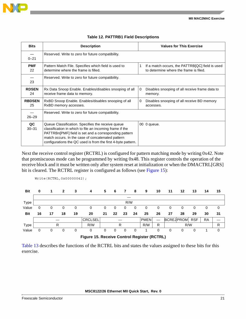
Next the receive control register (RCTRL) is configured for pattern matching mode by writing 0x42. Note that promiscuous mode can be programmed by writing 0x48. This register controls the operation of the receive block and it must be written only after system reset at initialization or when the DMACTRL[GRS] bit is cleared. The RCTRL register is configured as follows (see Figure 15):
Write(RCTRL,0x00000042);
Table 13 describes the functions of the RCTRL bits and states the values assigned to these bits for this exercise.
Table 12. PATTRB1 Field Descriptions
Bits Description Values for This Exercise
—0–21
Reserved. Write to zero for future compatibility.
PMF22
Pattern Match File. Specifies which field is used to determine where the frame is filled.
1 If a match occurs, the PATTRB[QC] field is used to determine where the frame is filed.
—23
Reserved. Write to zero for future compatibility.
RDSEN24
Rx Data Snoop Enable. Enables/disables snooping of all receive frame data to memory.
0 Disables snooping of all receive frame data to memory.
RBDSEN25
RxBD Snoop Enable. Enables/disables snooping of all RxBD memory accesses.
0 Disables snooping of all receive BD memory accesses.
—26–29
Reserved. Write to zero for future compatibility.
QC30–31
Queue Classification. Specifies the receive queue classification in which to file an incoming frame if the PATTRBn[PMF] field is set and a corresponding pattern match occurs. In the case of concatenated pattern configurations the QC used is from the first 4-byte pattern.
00 0 queue.
Bit 0 1 2 3 4 5 6 7 8 9 10 11 12 13 14 15
—
Type R/W
Value 0 0 0 0 0 0 0 0 0 0 0 0 0 0 0 0
Bit 16 17 18 19 20 21 22 23 24 25 26 27 28 29 30 31
— CRCLSEL — PMEN — BCREJ PROM RSF RA —
Type R R/W R R/W R R/W R
Value 0 0 0 0 0 0 0 0 0 1 0 0 0 0 1 0
Figure 15. Receive Control Register (RCTRL)
MSC8122/26 Ethernet MII Quick Start, Rev. 0
22 Freescale Semiconductor
MII MAC2MAC Exercise
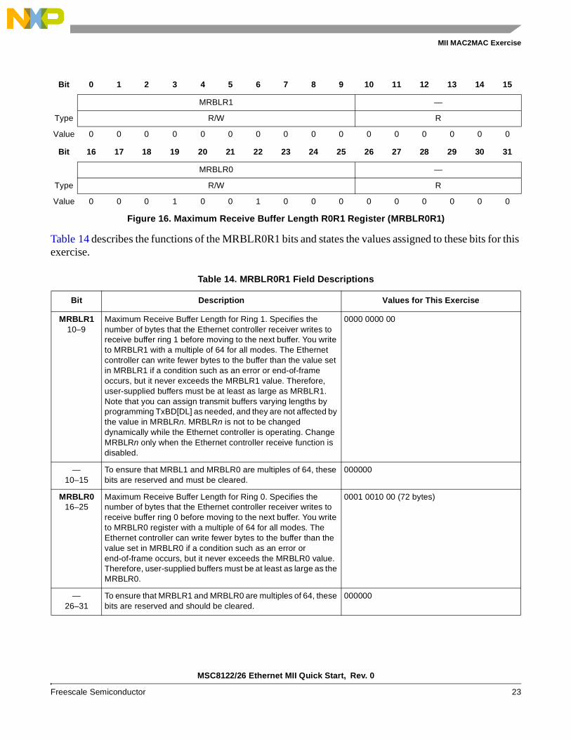
Next the maximum receive buffer length R0R1 Register (MRBLR0R1) is configured as follows (see Figure 16):
Write(MRBLR0R1,0x00001200);
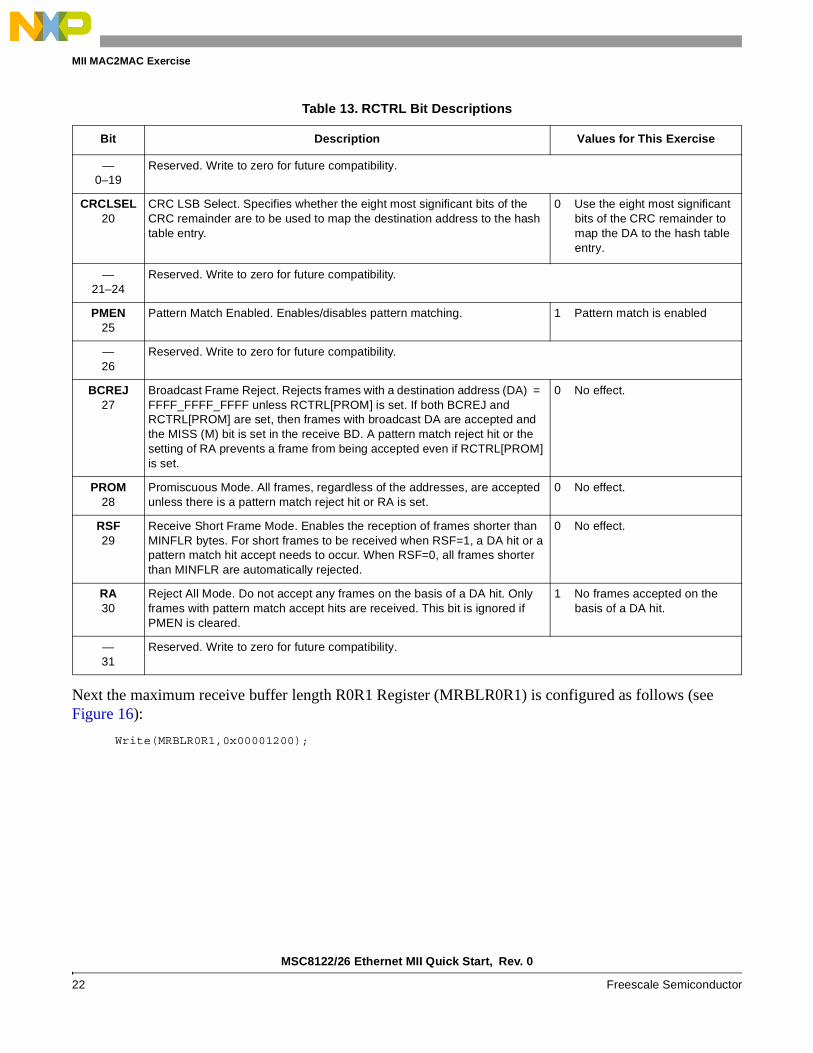
Table 13. RCTRL Bit Descriptions
Bit Description Values for This Exercise
—0–19
Reserved. Write to zero for future compatibility.
CRCLSEL20
CRC LSB Select. Specifies whether the eight most significant bits of the CRC remainder are to be used to map the destination address to the hash table entry.
0 Use the eight most significant bits of the CRC remainder to map the DA to the hash table entry.
—21–24
Reserved. Write to zero for future compatibility.
PMEN25
Pattern Match Enabled. Enables/disables pattern matching. 1 Pattern match is enabled
—26
Reserved. Write to zero for future compatibility.
BCREJ27
Broadcast Frame Reject. Rejects frames with a destination address (DA) = FFFF_FFFF_FFFF unless RCTRL[PROM] is set. If both BCREJ and RCTRL[PROM] are set, then frames with broadcast DA are accepted and the MISS (M) bit is set in the receive BD. A pattern match reject hit or the setting of RA prevents a frame from being accepted even if RCTRL[PROM] is set.
0 No effect.
PROM28
Promiscuous Mode. All frames, regardless of the addresses, are accepted unless there is a pattern match reject hit or RA is set.
0 No effect.
RSF29
Receive Short Frame Mode. Enables the reception of frames shorter than MINFLR bytes. For short frames to be received when RSF=1, a DA hit or a pattern match hit accept needs to occur. When RSF=0, all frames shorter than MINFLR are automatically rejected.
0 No effect.
RA30
Reject All Mode. Do not accept any frames on the basis of a DA hit. Only frames with pattern match accept hits are received. This bit is ignored if PMEN is cleared.
1 No frames accepted on the basis of a DA hit.
—31
Reserved. Write to zero for future compatibility.
MSC8122/26 Ethernet MII Quick Start, Rev. 0
Freescale Semiconductor 23
MII MAC2MAC Exercise
Table 14 describes the functions of the MRBLR0R1 bits and states the values assigned to these bits for this exercise.
Bit 0 1 2 3 4 5 6 7 8 9 10 11 12 13 14 15
MRBLR1 —
Type R/W R
Value 0 0 0 0 0 0 0 0 0 0 0 0 0 0 0 0
Bit 16 17 18 19 20 21 22 23 24 25 26 27 28 29 30 31
MRBLR0 —
Type R/W R
Value 0 0 0 1 0 0 1 0 0 0 0 0 0 0 0 0
Figure 16. Maximum Receive Buffer Length R0R1 Register (MRBLR0R1)
Table 14. MRBLR0R1 Field Descriptions
Bit Description Values for This Exercise
MRBLR110–9
Maximum Receive Buffer Length for Ring 1. Specifies the number of bytes that the Ethernet controller receiver writes to receive buffer ring 1 before moving to the next buffer. You write to MRBLR1 with a multiple of 64 for all modes. The Ethernet controller can write fewer bytes to the buffer than the value set in MRBLR1 if a condition such as an error or end-of-frame occurs, but it never exceeds the MRBLR1 value. Therefore, user-supplied buffers must be at least as large as MRBLR1. Note that you can assign transmit buffers varying lengths by programming TxBD[DL] as needed, and they are not affected by the value in MRBLRn. MRBLRn is not to be changed dynamically while the Ethernet controller is operating. Change MRBLRn only when the Ethernet controller receive function is disabled.
0000 0000 00
—10–15
To ensure that MRBL1 and MRBLR0 are multiples of 64, these bits are reserved and must be cleared.
000000
MRBLR016–25
Maximum Receive Buffer Length for Ring 0. Specifies the number of bytes that the Ethernet controller receiver writes to receive buffer ring 0 before moving to the next buffer. You write to MRBLR0 register with a multiple of 64 for all modes. The Ethernet controller can write fewer bytes to the buffer than the value set in MRBLR0 if a condition such as an error or end-of-frame occurs, but it never exceeds the MRBLR0 value. Therefore, user-supplied buffers must be at least as large as the MRBLR0.
0001 0010 00 (72 bytes)
—26–31
To ensure that MRBLR1 and MRBLR0 are multiples of 64, these bits are reserved and should be cleared.
000000
MSC8122/26 Ethernet MII Quick Start, Rev. 0
24 Freescale Semiconductor
MII MAC2MAC Exercise
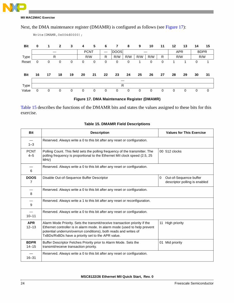
Next, the DMA maintenance register (DMAMR) is configured as follows (see Figure 17):
Write(DMAMR,0x004d0000);
Table 15 describes the functions of the DMAMR bits and states the values assigned to these bits for this exercise.
Bit 0 1 2 3 4 5 6 7 8 9 10 11 12 13 14 15
— PCNT — DOOS — APR BDPR
Type R R/W R R/W R/W R/W R/W R R/W R/W
Reset 0 0 0 0 0 0 0 0 0 1 0 0 1 1 0 1
Bit 16 17 18 19 20 21 22 23 24 25 26 27 28 29 30 31
—
Type R
Value 0 0 0 0 0 0 0 0 0 0 0 0 0 0 0 0
Figure 17. DMA Maintenance Register (DMAMR)
Table 15. DMAMR Field Descriptions
Bit Description Values for This Exercise
—1–3
Reserved. Always write a 0 to this bit after any reset or configuration.
PCNT4–5
Polling Count. This field sets the polling frequency of the transmitter. The polling frequency is proportional to the Ethernet MII clock speed (2.5, 25 MHz)
00 512 clocks
—6
Reserved. Always write a 0 to this bit after any reset or configuration.
DOOS7
Disable Out-of-Sequence Buffer Descriptor 0 Out-of-Sequence buffer descriptor polling is enabled
—8
Reserved. Always write a 0 to this bit after any reset or configuration.
—9
Reserved. Always write a 1 to this bit after any reset or reconfiguration.
—10–11
Reserved. Always write a 0 to this bit after any reset or configuration.
APR12–13
Alarm Mode Priority. Sets the transmit/receive transaction priority if the Ethernet controller is in alarm mode. In alarm mode (used to help prevent potential underrun/overrun conditions), both reads and writes of TxBDs/RxBDs have a priority set to the APR value.
11 High priority
BDPR14–15
Buffer Descriptor Fetches Priority prior to Alarm Mode. Sets the transmit/receive transaction priority.
01 Mid priority
—16–31
Reserved. Always write a 0 to this bit after any reset or configuration.
MSC8122/26 Ethernet MII Quick Start, Rev. 0
Freescale Semiconductor 25
MII MAC2MAC Exercise
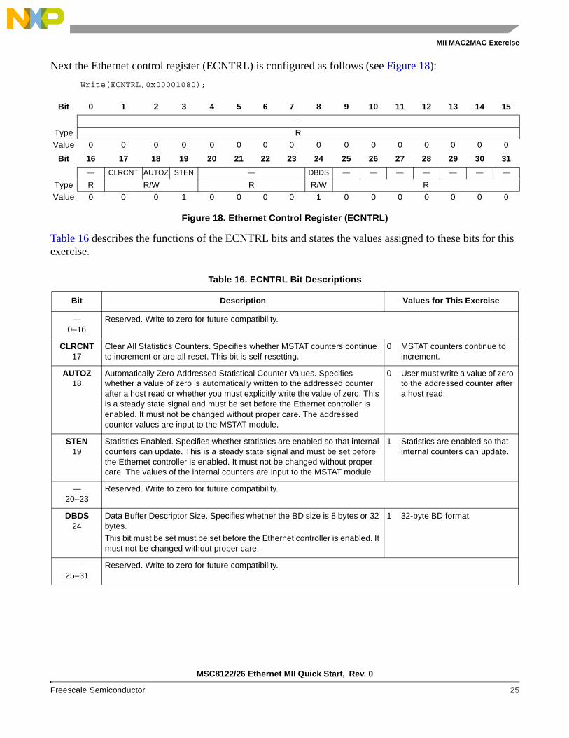
Next the Ethernet control register (ECNTRL) is configured as follows (see Figure 18):
Write(ECNTRL,0x00001080);
Table 16 describes the functions of the ECNTRL bits and states the values assigned to these bits for this exercise.
Bit 0 1 2 3 4 5 6 7 8 9 10 11 12 13 14 15
—
Type R
Value 0 0 0 0 0 0 0 0 0 0 0 0 0 0 0 0
Bit 16 17 18 19 20 21 22 23 24 25 26 27 28 29 30 31
— CLRCNT AUTOZ STEN — DBDS — — — — — — —
Type R R/W R R/W R
Value 0 0 0 1 0 0 0 0 1 0 0 0 0 0 0 0
Figure 18. Ethernet Control Register (ECNTRL)
Table 16. ECNTRL Bit Descriptions
Bit Description Values for This Exercise
—0–16
Reserved. Write to zero for future compatibility.
CLRCNT17
Clear All Statistics Counters. Specifies whether MSTAT counters continue to increment or are all reset. This bit is self-resetting.
0 MSTAT counters continue to increment.
AUTOZ18
Automatically Zero-Addressed Statistical Counter Values. Specifies whether a value of zero is automatically written to the addressed counter after a host read or whether you must explicitly write the value of zero. This is a steady state signal and must be set before the Ethernet controller is enabled. It must not be changed without proper care. The addressed counter values are input to the MSTAT module.
0 User must write a value of zero to the addressed counter after a host read.
STEN19
Statistics Enabled. Specifies whether statistics are enabled so that internal counters can update. This is a steady state signal and must be set before the Ethernet controller is enabled. It must not be changed without proper care. The values of the internal counters are input to the MSTAT module
1 Statistics are enabled so that internal counters can update.
—20–23
Reserved. Write to zero for future compatibility.
DBDS24
Data Buffer Descriptor Size. Specifies whether the BD size is 8 bytes or 32 bytes.
This bit must be set must be set before the Ethernet controller is enabled. It must not be changed without proper care.
1 32-byte BD format.
—25–31
Reserved. Write to zero for future compatibility.
MSC8122/26 Ethernet MII Quick Start, Rev. 0
26 Freescale Semiconductor
MII MAC2MAC Exercise
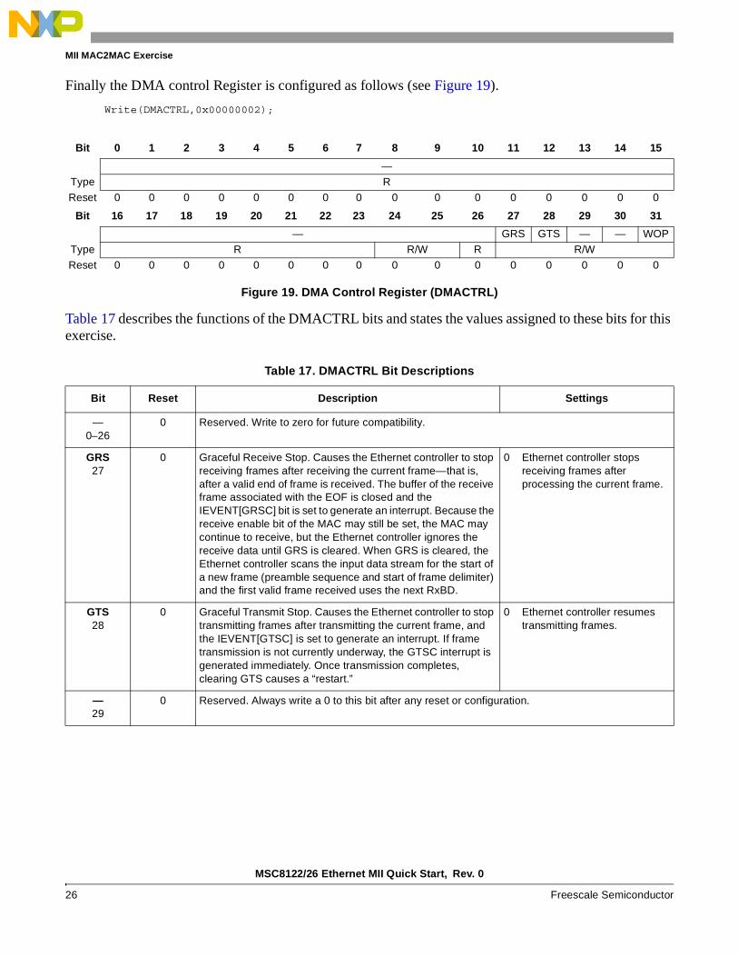
Finally the DMA control Register is configured as follows (see Figure 19).
Write(DMACTRL,0x00000002);
Table 17 describes the functions of the DMACTRL bits and states the values assigned to these bits for this exercise.
Bit 0 1 2 3 4 5 6 7 8 9 10 11 12 13 14 15
—
Type R
Reset 0 0 0 0 0 0 0 0 0 0 0 0 0 0 0 0
Bit 16 17 18 19 20 21 22 23 24 25 26 27 28 29 30 31
— GRS GTS — — WOP
Type R R/W R R/W
Reset 0 0 0 0 0 0 0 0 0 0 0 0 0 0 0 0
Figure 19. DMA Control Register (DMACTRL)
Table 17. DMACTRL Bit Descriptions
Bit Reset Description Settings
—0–26
0 Reserved. Write to zero for future compatibility.
GRS27
0 Graceful Receive Stop. Causes the Ethernet controller to stop receiving frames after receiving the current frame—that is, after a valid end of frame is received. The buffer of the receive frame associated with the EOF is closed and the IEVENT[GRSC] bit is set to generate an interrupt. Because the receive enable bit of the MAC may still be set, the MAC may continue to receive, but the Ethernet controller ignores the receive data until GRS is cleared. When GRS is cleared, the Ethernet controller scans the input data stream for the start of a new frame (preamble sequence and start of frame delimiter) and the first valid frame received uses the next RxBD.
0 Ethernet controller stops receiving frames after processing the current frame.
GTS28
0 Graceful Transmit Stop. Causes the Ethernet controller to stop transmitting frames after transmitting the current frame, and the IEVENT[GTSC] is set to generate an interrupt. If frame transmission is not currently underway, the GTSC interrupt is generated immediately. Once transmission completes, clearing GTS causes a “restart.”
0 Ethernet controller resumes transmitting frames.
—29
0 Reserved. Always write a 0 to this bit after any reset or configuration.
MSC8122/26 Ethernet MII Quick Start, Rev. 0
Freescale Semiconductor 27
MII MAC2MAC External Exercise
4 MII MAC2MAC External ExerciseAs long as the MSC8122ADS board is properly set up, everything is ready to run the MSC8122 Ethernet exercise. First download and run the host (MSC8101/3) project in AN3063SW, a zip file that accompanies this application note. Next, download and run the MSC8122 project. During the debug session a STDIO window appears and displays the following message.
Welcome to ENET MII test - Core number 1MIIGSK_ENR=3Check 8122 TXBDs8122: 1000 TXBDs were updated successfullyCheck 8103 TXBDs1000 Frames Were transmitted successfully From 8103Check 8103 RXBDs8103 : 1000 RXBDs were updated successfullyCheck 8122 Receive RXBDsChecking 1000 8122 RXBDs8122 1000 RXBDs were updated successfullyCheck 8103 TX data to 8122 Receive BuffersALL FRAMES FROM 8103 WERE ACCEPTEDCheck 8103 RX data from 8122 Transmit BuffersALL FRAMES FROM 8122 WERE ACCEPTED.
This I/O messages indicate that the test ran successfully and that the Ethernet frames were successfully exchanged. Also, the MAC2MAC exercise ran and completed successfully. Test mode requires the following preprocessor macro to be added into the project settings under the I/O and Preprocessors panel for both the host and slave projects.
DTEST_TYPE=MII_M2M_TPDTEST_SPEED=SPEED_100_MBPS
This exercise with both the host and slave CodeWarrior projects is available in the directory named MII_MAC2MAC_external\projects\feth_all_tests_fulld_gpio_and_dsi directory of AN3063SW.
There are only two differences between the MAC2MAC external and MAC2MAC internal loopback exercises:
• The register configuration for the MACCFG1 (MAC configuration register 1, specifically in the MIILB (bit 23), which is cleared to disable MII loopback mode.
• For the external loopback, all JP6 jumpers must be removed.
—30
0 Reserved. Always write a 1 to this bit after any reset or configuration.
WOP31
0 Wait or Poll. Provides the option for the Ethernet controller to poll a TxBD periodically or to wait for software to tell it to fetch a BD. In the “Wait” mode, the Ethernet controller allows two additional reads of a descriptor that is not ready before it enters a halt state. No interrupt is driven. To resume transmission, software must clear TSTAT[THLT].
0 Poll TxBD based on the setting of DMAMR[PCNT].
Table 17. DMACTRL Bit Descriptions (continued)
Bit Reset Description Settings
Document Number: AN3063Rev. 002/2006
Freescale™, the Freescale logo, and CodeWarrior are trademarks of Freescale Semiconductor, Inc. All other product or service names are the property of their respective owners.
© Freescale Semiconductor, Inc., 2006.
Information in this document is provided solely to enable system and software
implementers to use Freescale Semiconductor products. There are no express or
implied copyright licenses granted hereunder to design or fabricate any integrated
circuits or integrated circuits based on the information in this document.
Freescale Semiconductor reserves the right to make changes without further notice to
any products herein. Freescale Semiconductor makes no warranty, representation or
guarantee regarding the suitability of its products for any particular purpose, nor does
Freescale Semiconductor assume any liability arising out of the application or use of
any product or circuit, and specifically disclaims any and all liability, including without
limitation consequential or incidental damages. “Typical” parameters which may be
provided in Freescale Semiconductor data sheets and/or specifications can and do
vary in different applications and actual performance may vary over time. All operating
parameters, including “Typicals” must be validated for each customer application by
customer’s technical experts. Freescale Semiconductor does not convey any license
under its patent rights nor the rights of others. Freescale Semiconductor products are
not designed, intended, or authorized for use as components in systems intended for
surgical implant into the body, or other applications intended to support or sustain life,
or for any other application in which the failure of the Freescale Semiconductor product
could create a situation where personal injury or death may occur. Should Buyer
purchase or use Freescale Semiconductor products for any such unintended or
unauthorized application, Buyer shall indemnify and hold Freescale Semiconductor
and its officers, employees, subsidiaries, affiliates, and distributors harmless against all
claims, costs, damages, and expenses, and reasonable attorney fees arising out of,
directly or indirectly, any claim of personal injury or death associated with such
unintended or unauthorized use, even if such claim alleges that Freescale
Semiconductor was negligent regarding the design or manufacture of the part.
How to Reach Us:
Home Page: www.freescale.com
email: [email protected]
USA/Europe or Locations Not Listed: Freescale Semiconductor Technical Information Center, CH3701300 N. Alma School Road Chandler, Arizona 85224 [email protected]
Europe, Middle East, and Africa:Freescale Halbleiter Deutschland GmbHTechnical Information CenterSchatzbogen 781829 Muenchen, Germany+44 1296 380 456 (English) +46 8 52200080 (English)+49 89 92103 559 (German)+33 1 69 35 48 48 (French) [email protected]
Japan: Freescale Semiconductor Japan Ltd. HeadquartersARCO Tower 15F1-8-1, Shimo-Meguro, Meguro-ku Tokyo 153-0064, Japan 0120 191014+81 3 5437 [email protected]
Asia/Pacific: Freescale Semiconductor Hong Kong Ltd. Technical Information Center2 Dai King Street Tai Po Industrial Estate, Tai Po, N.T., Hong Kong +800 2666 [email protected]
For Literature Requests Only:Freescale Semiconductor
Literature Distribution Center P.O. Box 5405Denver, Colorado 80217 1-800-441-2447303-675-2140Fax: 303-675-2150LDCForFreescaleSemiconductor
@hibbertgroup.com