MSC035SMA170S Silicon Carbide N-Channel Power MOSFET
13
MSC035SMA170S Silicon Carbide N-Channel Power MOSFET Product Overview The silicon carbide (SiC) power MOSFET product line from Microsemi increases the performance over silicon MOSFET and silicon IGBT solutions while lowering the total cost of ownership for high-voltage applications. The MSC035SMA170S device is a 1700 V, 35 mΩ SiC MOSFET in a TO-268 (D3PAK) package. Features The following are key features of the MSC035SMA170S device: • Low capacitances and low gate charge • Fast switching speed due to low internal gate resistance (ESR) • Stable operation at high junction temperature, T J(max) = 175 °C • Fast and reliable body diode • Superior avalanche ruggedness • RoHS compliant Benefits The following are benefits of the MSC035SMA170S device: • High efficiency to enable lighter, more compact system • Simple to drive and easy to parallel • Improved thermal capabilities and lower switching losses • Eliminates the need for external freewheeling diode • Lower system cost of ownership Applications The MSC035SMA170S device is designed for the following applications: • PV inverter, converter, and industrial motor drives • Smart grid transmission and distribution • Induction heating and welding • H/EV powertrain and EV charger • Power supply and distribution 1 050-7771 MSC035SMA170S Datasheet Revision A
Transcript of MSC035SMA170S Silicon Carbide N-Channel Power MOSFET

MSC035SMA170S Silicon Carbide N-Channel Power MOSFET
Product Overview
The silicon carbide (SiC) powerMOSFET product line fromMicrosemi increases the performance over siliconMOSFET and silicon IGBT solutions while lowering the total cost of ownership for high-voltage applications.The MSC035SMA170S device is a 1700 V, 35 mΩ SiC MOSFET in a TO-268 (D3PAK) package.
Features
The following are key features of the MSC035SMA170S device:• Low capacitances and low gate charge• Fast switching speed due to low internal gate resistance (ESR)• Stable operation at high junction temperature, TJ(max) = 175 °C• Fast and reliable body diode• Superior avalanche ruggedness• RoHS compliant
Benefits
The following are benefits of the MSC035SMA170S device:• High efficiency to enable lighter, more compact system• Simple to drive and easy to parallel• Improved thermal capabilities and lower switching losses• Eliminates the need for external freewheeling diode• Lower system cost of ownership
Applications
The MSC035SMA170S device is designed for the following applications:• PV inverter, converter, and industrial motor drives• Smart grid transmission and distribution• Induction heating and welding• H/EV powertrain and EV charger• Power supply and distribution
1050-7771 MSC035SMA170S Datasheet Revision A
Device Specifications
This section shows the specifications of the MSC035SMA170S device.
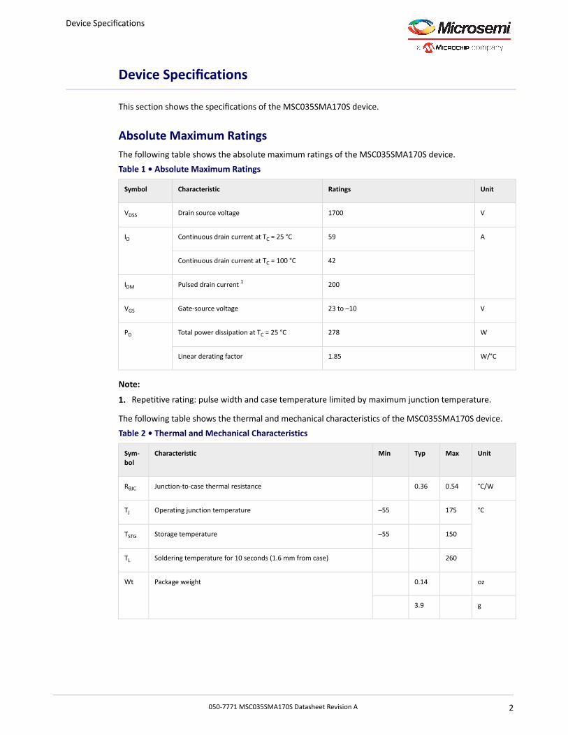
Absolute Maximum RatingsThe following table shows the absolute maximum ratings of the MSC035SMA170S device.Table 1 • Absolute Maximum Ratings
UnitRatingsCharacteristicSymbol
V1700Drain source voltageVDSS
A59Continuous drain current at TC = 25 °CID
42Continuous drain current at TC = 100 °C
200Pulsed drain current 1IDM
V23 to –10Gate-source voltageVGS
W278Total power dissipation at TC = 25 °CPD
W/°C1.85Linear derating factor
Note:
1. Repetitive rating: pulse width and case temperature limited by maximum junction temperature.
The following table shows the thermal and mechanical characteristics of the MSC035SMA170S device.Table 2 • Thermal and Mechanical Characteristics
UnitMaxTypMinCharacteristicSym-bol
°C/W0.540.36Junction-to-case thermal resistanceRθJC
°C175–55Operating junction temperatureTJ
150–55Storage temperatureTSTG
260Soldering temperature for 10 seconds (1.6 mm from case)TL
oz0.14Package weightWt
g3.9
2050-7771 MSC035SMA170S Datasheet Revision A
Device Specifications

Electrical PerformanceThe following table shows the static characteristics of the MSC035SMA170S device. TJ = 25 °C unlessotherwise specified.Table 3 • Static Characteristics
UnitMaxTypMinTest ConditionsCharacteristicSymbol
V1700VGS = 0 V, I D = 100 µADrain-source breakdown voltageV(BR) DSS
mΩ4535VGS = 20 V, ID = 30 ADrain-source on resistance1RDS(on)
V3.251.8VGS = VDS, ID = 2.5 mAGate-source threshold voltageVGS(th)
mV/°C–5.1V GS = V DS, I D = 2.5 mAThreshold voltage coefficientΔVGS(th)/ΔTJ
µA100VDS = 1700 V, VGS = 0 VZero gate voltage drain currentIDSS
500V DS = 1700 V, V GS = 0 V
T J = 125 °C
nA±100VGS = 20 V/–10 VGate-source leakage currentIGSS
Note:
1. Pulse test: pulse width < 380 µs, duty cycle < 2%.
The following table shows the dynamic characteristics of the MSC035SMA170S device. TJ = 25 °C unlessotherwise specified.Table 4 • Dynamic Characteristics
UnitMaxTypMinTest ConditionsCharacteristicSymbol
pF3300VGS = 0 V, VDD = 1000 V
VAC = 25 mV, ƒ = 1 MHz
Input capacitanceC iss
10Reverse transfer capacitanceCrss
150Output capacitanceCoss
nC178VGS = –5 V/20 V, VDD = 850 V
ID = 30 A
Total gate chargeQg
49Gate-source chargeQgs
27Gate-drain chargeQgd
ns38VDD = 1200 V, VGS = –5 V/20 V
ID = 50 A, R G(ext) = 4 Ω1,
Turn-on delay timetd(on)
20Voltage fall timetf Freewheeling diode =
MSC035SMA170S (Vg = –5 V)
3050-7771 MSC035SMA170S Datasheet Revision A
Device Specifications

UnitMaxTypMinTest ConditionsCharacteristicSymbol
26Turn-off delay timetd(off)
10Voltage rise timetr
µJ2743Turn-on switching energy 2Eon
368Turn-off switching energyEoff
ns38VDD = 1200 V, VGS = –5 V/20 V
ID = 50 A, RG(ext) = 4 Ω1,
Turn-on delay timetd(on)
20Voltage fall timetf Freewheeling diode =
MSC050SDA170B26Turn-off delay timetd(off)
10Voltage rise timetr
µJ2820Turn-on switching energy 2Eon
368Turn-off switching energyEoff
Ω0.85f = 1 MHz, 25 mV, drain shortEquivalent series resistanceESR
µs3VDS = 1200 V, VGS = 20 VShort circuit withstand timeSCWT
mJ4000VDS = 150 V, VGS = 20 V, ID = 30 AAvalanche energy, single pulseEAS
Notes:
1. RG is total gate resistance excluding internal gate driver impedance.
2. Eon includes energy of the freewheeling diode.
4050-7771 MSC035SMA170S Datasheet Revision A
Device Specifications

The following table shows the body diode characteristics of the MSC035SMA170S device. TJ = 25 °C unlessotherwise specified.Table 5 • Body Diode Characteristics
UnitMaxTypMinTest ConditionsCharacteristicSymbol
V3.7ISD = 30 A, VGS = 0 VDiode forward voltageVSD
V3.9I SD = 30 A, V GS = –5 V
ns42ISD = 50 A, VGS = –5 V,
VDD = 1200 V, dl/dt = –1900 A/µs
Reverse recovery timetrr
nC510Reverse recovery chargeQrr
A18Reverse recovery currentI RRM
Typical Performance CurvesThis section shows the typical performance curves of the MSC035SMA170S device.
Figure 2 • Drain Current vs. VDSFigure 1 • Drain Current vs. VDS
5050-7771 MSC035SMA170S Datasheet Revision A
Device Specifications

Figure 4 • Drain Current vs. VDSFigure 3 • Drain Current vs. VDS
Figure 6 • Gate Charge CharacteristicsFigure 5 • RDS(on) vs. Junction Temperature
6050-7771 MSC035SMA170S Datasheet Revision A
Device Specifications

Figure 8 • IDM vs. Gate-to-Source VoltageFigure 7 • Capacitance vs. Drain-to-Source Voltage
Figure 10 • IDM vs. VDS 3rd Quadrant ConductionFigure 9 • IDM vs. VDS 3
rd Quadrant Conduction
7050-7771 MSC035SMA170S Datasheet Revision A
Device Specifications
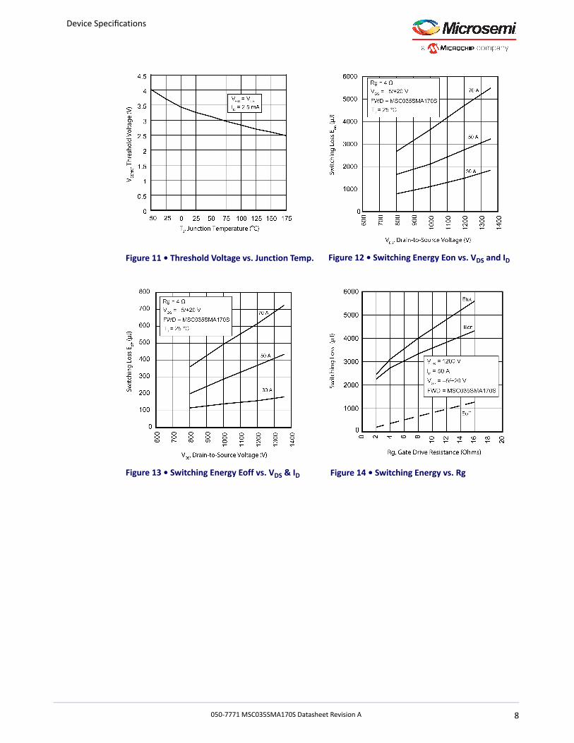
Figure 12 • Switching Energy Eon vs. VDS and IDFigure 11 • Threshold Voltage vs. Junction Temp.
Figure 14 • Switching Energy vs. RgFigure 13 • Switching Energy Eoff vs. VDS & ID
8050-7771 MSC035SMA170S Datasheet Revision A
Device Specifications

Figure 16 • Switching Energy Eon vs. VDS and IDFigure 15 • Switching Energy vs. TJ
Figure 18 • Switching Energy vs. RgFigure 17 • Switching Energy Eoff vs. VDS and ID
9050-7771 MSC035SMA170S Datasheet Revision A
Device Specifications

Figure 20 • Forward Safe Operating AreaFigure 19 • Switching Energy vs. TJ
Figure 21 • Maximum Transient Thermal Impedance
10050-7771 MSC035SMA170S Datasheet Revision A
Device Specifications

Package Specification
This section shows the package specification of the MSC035SMA170S device.
Package Outline DrawingThe following figure illustrates the TO-268 package drawing for theMSC035SMA170Sdevice. The dimensionsin the figure below are in millimeters and (inches).
Figure 22 • Package Outline Drawing
The following table shows the TO-268 dimensions and should be used in conjunction with the packageoutline drawing.Table 6 • TO-268 Dimensions
Max (in.)Min (in.)Max (mm)Min (mm)Symbol
0.2010.1935.104.90A
0.6380.62416.2015.85B
0.7520.73619.1018.70C
0.0490.0391.251.00D
0.5510.54314.0013.80E
0.5350.52413.6013.30F
11050-7771 MSC035SMA170S Datasheet Revision A
Package Specification

Max (in.)Min (in.)Max (mm)Min (mm)Symbol
0.1140.1062.902.70G
0.0570.0451.451.15H
0.0870.0772.211.95I
0.0550.0371.400.94J
0.1060.0942.702.40K
0.0240.0160.600.40L
0.0630.0571.601.45M
0.0070.0000.180.00N
0.5000.48812.7012.40O
0.215 BSC (nom.)5.45 BSC (nom.)P
GateTerminal 1
DrainTerminal 2
SourceTerminal 3
DrainTerminal 4
12050-7771 MSC035SMA170S Datasheet Revision A
Package Specification

Microsemi's product warranty is set forth inMicrosemi's Sales Order Terms and Conditions. Informationcontained in this publication is provided for the sole purpose of designing with and using Microsemiproducts. Information regarding device applications and the like is provided only for your convenienceand may be superseded by updates. Buyer shall not rely on any data and performance specifications orparameters provided by Microsemi. It is your responsibility to ensure that your application meets withyour specifications. THIS INFORMATION IS PROVIDED "AS IS."MICROSEMIMAKESNOREPRESENTATIONSOR WARRANTIES OF ANY KIND WHETHER EXPRESS OR IMPLIED, WRITTEN OR ORAL, STATUTORY OROTHERWISE, RELATED TOTHE INFORMATION, INCLUDINGBUTNOT LIMITEDTO ITS CONDITION,QUALITY,PERFORMANCE, NON-INFRINGEMENT, MERCHANTABILITY OR FITNESS FOR A PARTICULAR PURPOSE.IN NO EVENT WILL MICROSEMI BE LIABLE FOR ANY INDIRECT, SPECIAL, PUNITIVE, INCIDENTAL ORCONSEQUENTIAL LOSS, DAMAGE, COST OR EXPENSE WHATSOEVER RELATED TO THIS INFORMATIONOR ITS USE, HOWEVER CAUSED, EVEN IF MICROSEMI HAS BEEN ADVISED OF THE POSSIBILITY OR THEDAMAGESARE FORESEEABLE. TOTHE FULLEST EXTENTALLOWEDBY LAW,MICROSEMI’S TOTAL LIABILITYON ALL CLAIMS IN RELATED TO THIS INFORMATION OR ITS USE WILL NOT EXCEED THE AMOUNT OFFEES, IF ANY, YOU PAID DIRECTLY TO MICROSEMI FOR THIS INFORMATION. Use of Microsemi devicesin life support, mission-critical equipment or applications, and/or safety applications is entirely at thebuyer’s risk, and the buyer agrees to defend and indemnifyMicrosemi from any and all damages, claims,suits, or expenses resulting from such use. No licenses are conveyed, implicitly or otherwise, under anyMicrosemi intellectual property rights unless otherwise stated.
Microsemi2355 W. Chandler Blvd.Chandler, AZ 85224 USA
Within the USA: +1 (480) 792-7200Fax: +1 (480) 792-7277
www.microsemi.com © 2020 Microsemi andits corporate affiliates. All rights reserved.Microsemi and the Microsemi logo aretrademarks of Microsemi Corporation and itscorporate affiliates. All other trademarks andservice marks are the property of theirrespective owners. Microsemi Corporation, a subsidiary ofMicrochip Technology Inc. (Nasdaq:MCHP),
and its corporate affiliates are leading providers of smart, connected and secureembedded control solutions. Their easy-to-use development tools andcomprehensive product portfolio enable customers to create optimal designswhichreduce risk while lowering total system cost and time to market. These solutionsserve more than 120,000 customers across the industrial, automotive, consumer,aerospace and defense, communications and computing markets. Headquarteredin Chandler, Arizona, the company offers outstanding technical support along withdependable delivery and quality. Learn more at www.microsemi.com.
050-7771 | April 2020 | Released
13050-7771 MSC035SMA170S Datasheet Revision A
Legal