MPMC Course File - gee · PDF fileContents required for course file 1. Cover Page 2. ......
210
MPMC Course File
Transcript of MPMC Course File - gee · PDF fileContents required for course file 1. Cover Page 2. ......
MPMC
Course File
Contents required for course file
1. Cover Page
2. Syllabus copy
3. Vision of the Department
4. Mission of the Department
5. PEOs and POs
6. Course objectives and outcomes
7. Brief notes on the importance of the course and how it fits into the curriculum
8. prerequisites
9. Instructional Learning Outcomes
10. Course mapping with PEOs and POs
11. Class Time Table
12. Individual Time Table
13. Micro Plan with dates and closure report
14. Detailed notes
15. Additional topics
16. University Question papers of previous years
17. Question Bank
18. Assignment topics
19. Unit wise Quiz Questions
20. Tutorial problems
21. Known gaps ,if any
22. Discussion topics
23. References, Journals, websites and E-links
24. Quality Control Sheets
25. Student List
26. Group-Wise students list for discussion topics

1.cover page GEETHANJALI COLLEGE OF ENGINEERING AND TECHNOLOGY
DEPARTMENT OF Electronics and Communication Engineering
(Name of the Subject ) : Microprocessors and Microcontrollers Course file
(JNTU CODE – A60430) Programme : UG
Branch: ECE Version No : 0
Year: III Document No: GCET/ECE/56012/01
Semester: II No. of pages :
Classification status (Unrestricted / Restricted ) : Unrestricted
Distribution List : Dept. Library, Dept Office, Concerned Faculty
Prepared by
1) Name : M.Laxmi/ P.Sneha Naga Shilpa/D.Sony/M.V.Sireesha
2) Sign :
3) Design : Assoc. Professor/Asst. Professors
4) Date : 25/11/2015
Verified by : 1) Name :
2) Sign :
3) Design :
4) Date :
* For Q.C Only.
1) Name :
2) Sign :
3) Design :
4) Date :
Approved by : (HOD ) 1) Name : Dr.P.Sri Hari
2) Sign :
3) Date :
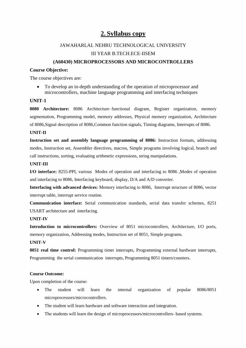
2. Syllabus copy
JAWAHARLAL NEHRU TECHNOLOGICAL UNIVERSITY
III YEAR B.TECH.ECE-IISEM
(A60430) MICROPROCESSORS AND MICROCONTROLLERS
Course Objective:
The course objectives are:
To develop an in-depth understanding of the operation of microprocessor and
microcontrollers, machine language programming and interfacing techniques
UNIT-1
8080 Architecture: 8086 Architecture–functional diagram, Register organization, memory
segmentation, Programming model, memory addresses, Physical memory organization, Architecture
of 8086,Signal description of 8086,Common function signals, Timing diagrams, Interrupts of 8086.
UNIT-II
Instruction set and assembly language programming of 8086: Instruction formats, addressing
modes, Instruction set, Assembler directives, macros, Simple programs involving logical, branch and
call instructions, sorting, evaluating arithmetic expressions, string manipulations.
UNIT-III
I/O interface: 8255-PPI, various Modes of operation and interfacing to 8086 ,Modes of operation
and interfacing to 8086, Interfacing keyboard, display, D/A and A/D converter.
Interfacing with advanced devices: Memory interfacing to 8086, Interrupt structure of 8086, vector
interrupt table, interrupt service routine.
Communication interface: Serial communication standards, serial data transfer schemes, 8251
USART architecture and interfacing.
UNIT-IV
Introduction to microcontrollers: Overview of 8051 microcontrollers, Architecture, I/O ports,
memory organization, Addressing modes, Instruction set of 8051, Simple programs.
UNIT-V
8051 real time control: Programming timer interrupts, Programming external hardware interrupts,
Programming the serial communication interrupts, Programming 8051 timers/counters.
Course Outcome:
Upon completion of the course:
The student will learn the internal organization of popular 8086/8051
microprocessors/microcontrollers.
The student will learn hardware and software interaction and integration.
The students will learn the design of microprocessors/microcontrollers- based systems.
3.Vision of the Department
To impart quality technical education in Electronics and Communication Engineering
emphasizing analysis, design/synthesis and evaluation of hardware/embedded software using
various Electronic Design Automation (EDA) tools with accent on creativity, innovation and
research thereby producing competent engineers who can meet global challenges with
societal commitment.
4. Mission of the Department
i. To impart quality education in fundamentals of basic sciences, mathematics, electronics
and communication engineering through innovative teaching-learning processes.
ii. To facilitate Graduates define, design, and solve engineering problems in the field of
Electronics and Communication Engineering using various Electronic Design Automation
(EDA) tools.
iii. To encourage research culture among faculty and students thereby facilitating them to be
creative and innovative through constant interaction with R & D organizations and
Industry.
iv. To inculcate teamwork, imbibe leadership qualities, professional ethics and social
responsibilities in students and faculty
5.PEOs and POs
Program Educational Objectives of B. Tech (ECE) Program :
I. To prepare students with excellent comprehension of basic sciences, mathematics and
engineering subjects facilitating them to gain employment or pursue postgraduate
studies with an appreciation for lifelong learning.
II. To train students with problem solving capabilities such as analysis and design with
adequate practical skills wherein they demonstrate creativity and innovation that
would enable them to develop state of the art equipment and technologies of
multidisciplinary nature for societal development.
III. To inculcate positive attitude, professional ethics, effective communication and
interpersonal skills which would facilitate them to succeed in the chosen profession
exhibiting creativity and innovation through research and development both as team
member and as well as leader.
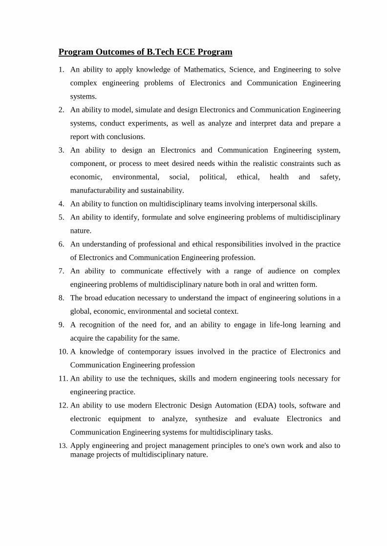
Program Outcomes of B.Tech ECE Program
1. An ability to apply knowledge of Mathematics, Science, and Engineering to solve
complex engineering problems of Electronics and Communication Engineering
systems.
2. An ability to model, simulate and design Electronics and Communication Engineering
systems, conduct experiments, as well as analyze and interpret data and prepare a
report with conclusions.
3. An ability to design an Electronics and Communication Engineering system,
component, or process to meet desired needs within the realistic constraints such as
economic, environmental, social, political, ethical, health and safety,
manufacturability and sustainability.
4. An ability to function on multidisciplinary teams involving interpersonal skills.
5. An ability to identify, formulate and solve engineering problems of multidisciplinary
nature.
6. An understanding of professional and ethical responsibilities involved in the practice
of Electronics and Communication Engineering profession.
7. An ability to communicate effectively with a range of audience on complex
engineering problems of multidisciplinary nature both in oral and written form.
8. The broad education necessary to understand the impact of engineering solutions in a
global, economic, environmental and societal context.
9. A recognition of the need for, and an ability to engage in life-long learning and
acquire the capability for the same.
10. A knowledge of contemporary issues involved in the practice of Electronics and
Communication Engineering profession
11. An ability to use the techniques, skills and modern engineering tools necessary for
engineering practice.
12. An ability to use modern Electronic Design Automation (EDA) tools, software and
electronic equipment to analyze, synthesize and evaluate Electronics and
Communication Engineering systems for multidisciplinary tasks.
13. Apply engineering and project management principles to one's own work and also to
manage projects of multidisciplinary nature.
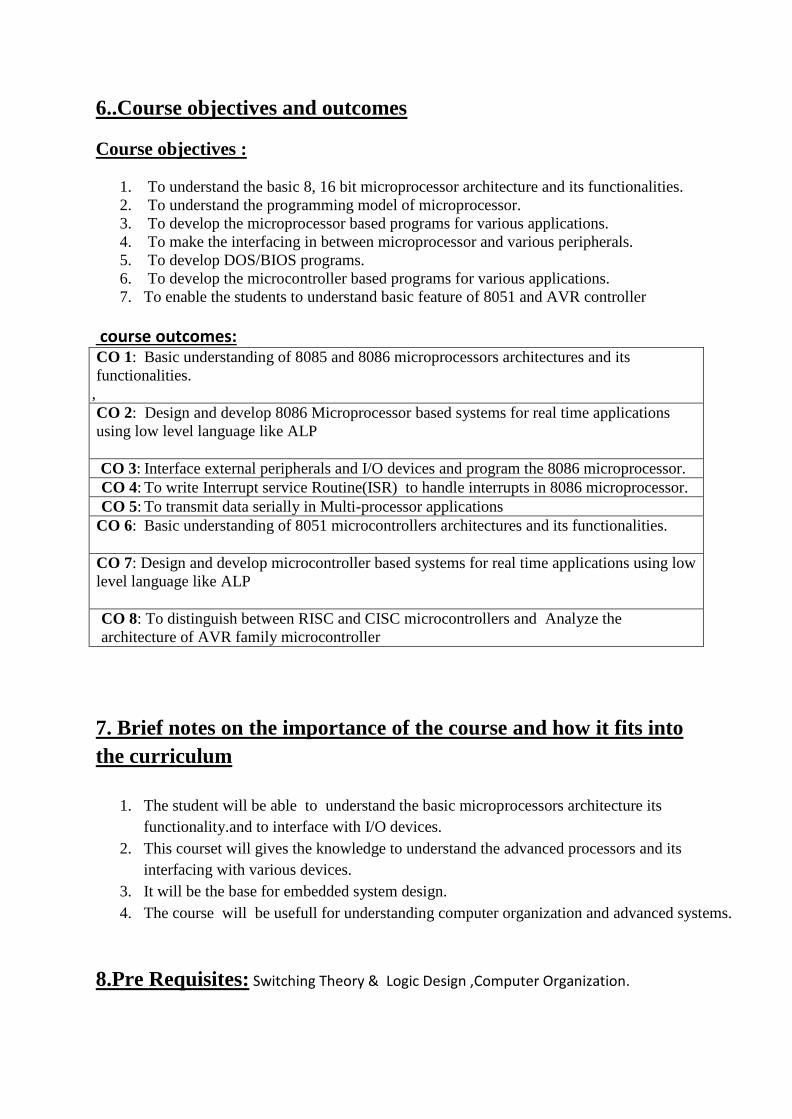
6..Course objectives and outcomes
Course objectives :
1. To understand the basic 8, 16 bit microprocessor architecture and its functionalities.
2. To understand the programming model of microprocessor.
3. To develop the microprocessor based programs for various applications.
4. To make the interfacing in between microprocessor and various peripherals.
5. To develop DOS/BIOS programs.
6. To develop the microcontroller based programs for various applications.
7. To enable the students to understand basic feature of 8051 and AVR controller
course outcomes: CO 1: Basic understanding of 8085 and 8086 microprocessors architectures and its
functionalities.
,
CO 2: Design and develop 8086 Microprocessor based systems for real time applications
using low level language like ALP
CO 3: Interface external peripherals and I/O devices and program the 8086 microprocessor.
CO 4: To write Interrupt service Routine(ISR) to handle interrupts in 8086 microprocessor.
CO 5: To transmit data serially in Multi-processor applications
CO 6: Basic understanding of 8051 microcontrollers architectures and its functionalities.
CO 7: Design and develop microcontroller based systems for real time applications using low
level language like ALP
CO 8: To distinguish between RISC and CISC microcontrollers and Analyze the
architecture of AVR family microcontroller
7. Brief notes on the importance of the course and how it fits into
the curriculum
1. The student will be able to understand the basic microprocessors architecture its
functionality.and to interface with I/O devices.
2. This courset will gives the knowledge to understand the advanced processors and its
interfacing with various devices.
3. It will be the base for embedded system design.
4. The course will be usefull for understanding computer organization and advanced systems.
8.Pre Requisites: Switching Theory & Logic Design ,Computer Organization.
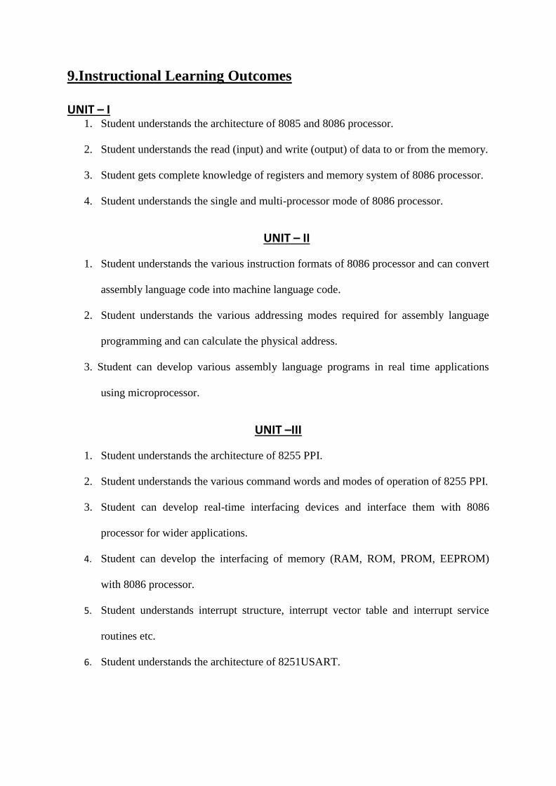
9.Instructional Learning Outcomes
UNIT – I
1. Student understands the architecture of 8085 and 8086 processor.
2. Student understands the read (input) and write (output) of data to or from the memory.
3. Student gets complete knowledge of registers and memory system of 8086 processor.
4. Student understands the single and multi-processor mode of 8086 processor.
UNIT – II
1. Student understands the various instruction formats of 8086 processor and can convert
assembly language code into machine language code.
2. Student understands the various addressing modes required for assembly language
programming and can calculate the physical address.
3. Student can develop various assembly language programs in real time applications
using microprocessor.
UNIT –III
1. Student understands the architecture of 8255 PPI.
2. Student understands the various command words and modes of operation of 8255 PPI.
3. Student can develop real-time interfacing devices and interface them with 8086
processor for wider applications.
4. Student can develop the interfacing of memory (RAM, ROM, PROM, EEPROM)
with 8086 processor.
5. Student understands interrupt structure, interrupt vector table and interrupt service
routines etc.
6. Student understands the architecture of 8251USART.
7. Student understands the various command words, modes of operation and interfacing
of 8251 USART with 8086 processor.
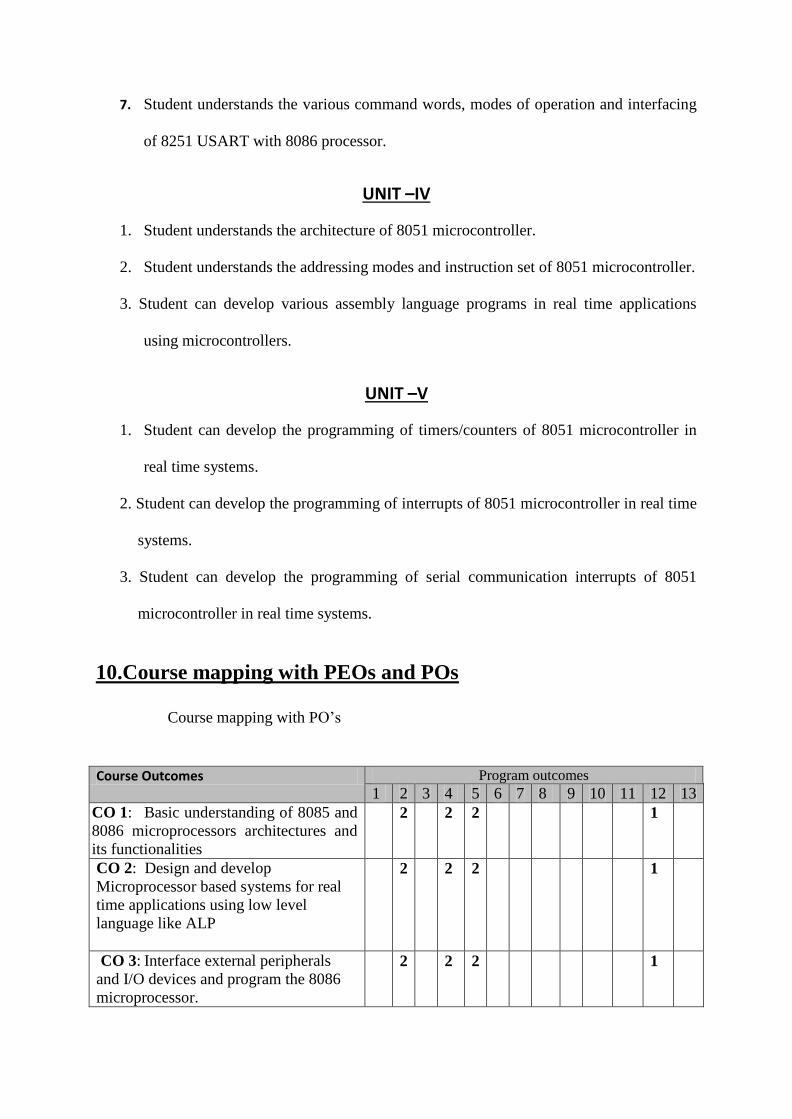
UNIT –IV
1. Student understands the architecture of 8051 microcontroller.
2. Student understands the addressing modes and instruction set of 8051 microcontroller.
3. Student can develop various assembly language programs in real time applications
using microcontrollers.
UNIT –V
1. Student can develop the programming of timers/counters of 8051 microcontroller in
real time systems.
2. Student can develop the programming of interrupts of 8051 microcontroller in real time
systems.
3. Student can develop the programming of serial communication interrupts of 8051
microcontroller in real time systems.
10.Course mapping with PEOs and POs
Course mapping with PO‘s
Course Outcomes Program outcomes
1 2 3 4 5 6 7 8 9 10 11 12 13
CO 1: Basic understanding of 8085 and
8086 microprocessors architectures and
its functionalities
2 2 2 1
CO 2: Design and develop
Microprocessor based systems for real
time applications using low level
language like ALP
2 2 2 1
CO 3: Interface external peripherals
and I/O devices and program the 8086
microprocessor.
2 2 2 1
CO 4: To write Interrupt service
Routine(ISR) to handle interrupts in
8086 microprocessor.
2 2 2 1
CO 5: To transmit data serially in
Multi-processor applications 2 2 2 1
CO 6: Basic understanding of 8051
microcontrollers architectures and its
functionalities
2 2 2 1
CO 7: Design and develop
microcontroller based systems for real
time applications using low level
language like ALP
2 2 2 1
CO 8: To distinguish between RISC
and CISC microcontrollers and
Analyze the architecture of AVR
family microcontroller
2 2 2 1
Course mapping with PEOs
PROGRAMME EDUCATIONAL OBJECTIVES
Domai
n
knowle
dge
Professi
onal
Employ
ment
High
er
Degr
ees
Enginee
ring
citizensh
ip
Lifelo
ng
Learn
ing
Research
and
Develop
ment
a) an ability to apply
the knowledge of
Mathematics, science
and engineering in
Electronics and
communications
√ √ √ √ √ √
b) an ability to Design
& Conduct
Experiments, as well as
analyze & Interpret
Data
√ √ √ √ √ √
c) an ability to design a
system, component, or
process to meet desired
needs with in realistic
constraints such as
economic,
environmental, social,
political, ethical, health
and safety,
manufacturability, and
√ √ √ √ √
sustainability
d) an ability to function
on multidisciplinary
teams
√ √ √ √
e) an ability to Identify,
Formulate & Solve
problems in the area of
Electronics and
Communications
Engineering
√ √ √
√ √
h) the broad education
necessary to understand
the impact of
engineering solutions
in a global, economic,
environmental, and
societal context
√ √ √
√ √
i) a recognition of the
need for, and an ability
to engage in life-long
learning
√ √ √ √ √ √
k) an ability to use the
techniques, skills, and
modern engineering
tools necessary for
engineering practice
√ √ √ √ √ √
12. Class Time Table
Hard copies are attached
13.Micro Plan:
Name of the FacultyM.Laxmi/P.Sneha Naga Shilpa/D.Sony/M.V.Sireesha
Branch: ECE
Year & Sem: III-II
Subject: Microprocessors and microcontrollers
Lesson Plan
S.L
no
Unit
No
Total no of
Periods
Topics to be covered Reg/
Additional
Teaching aids used
LCD/OHP/BB
Remarks
1 1 11 Overview of basics from Switching Theory & Logic Design and Computer Organization.
Additional BB
2 Overview of MPMC syllabus and its
importance in Real world
Additional BB
3 Evolution of microprocessors and
Introduction to 8085 microprocessor,
Additional OHP,BB
4 Architecture of 8086 Microprocessor –
functional diagram description
Regular OHP,BB
5 Register organization, memory
segmentation
Regular OHP,BB
6 Programming model, memory addresses Regular OHP,BB
7 Physical memory organization Regular BB
8 Signal description of 8086, Common
function signals
Regular BB
9 maximum and minimum mode signals Regular BB
10 Timing diagrams, Interrupts of 8086 Regular OHP,BB
11 Tutorial class Regular BB
12 II 08 Instruction formats, addressing modes Regular OHP,BB
13 Instruction set of 8086 Regular BB
14 Instruction set of 8086 Regular BB
15 Assembler directives, macros Regular OHP,BB
16 Simple programs on logical ,branch and
call instructions
Regular BB
17 Programs on sorting, string
manipulations
Regular BB
18 Tutorial class Regular BB
19 Introduction to Pentium and dual core
processors
Additional OHP,BB
20 III 20 Introduction to parallel data transfer
methods and importance of port structure
Regular OHP,BB
21 8255-PPI Regular OHP,BB
22 Modes of operation and interfacing to
8086
Regular BB
23 Modes of operation and interfacing to
8086
Regular BB
24 Interfacing keyboard, display to 8086 Regular OHP,BB
25 Stepper motor interfacing to 8086 Missing BB
26 A/D converter interfacing to 8086 Regular OHP,BB
27 D/A converter interfacing to 8086 Regular BB
28 Tutorial class Regular LCD,OHP,BB
29 Memory interfacing to 8086 Regular OHP,BB
30 Memory interfacing to 8086 Regular BB
32 Interrupt structure of 8086,vector
interrupt table, interrupt service routine
Regular OHP,BB
34 Introduction to DOS and BIOS
interrupts
Missing BB
35 Interrupt controller-8259, Interfacing
DMA controller 8257 to 8086
Additional BB
36 Tutorial class Regular OHPBB
37 8251 USART architecture Regular BB
8251 USART interfacing Regular BB
38 RS-232,IEEE 488 Standards Missing OHP,BB
39 Prototyping and troubleshooting Missing OHP,BB
40 TTL to RS 232 and
RS-232 to TTL conversion
Missing BB
41 IV 08 Overview of 8051 microcontrollers Regular OHP,BB
42 Architecture of 8051microcontroller Regular BB
43 I/O ports, memory segmentation of 8051 Regular BB
44 Addressing modes of 8051 Regular BB
45 Instruction set of 8051 Regular BB
46 Simple programs on 8051 Regular BB
47 Simple programs on 8051 Regular OHP,BB
49 Tutorial class Regular OHP,BB
50 V 10 Interrupts of 8051 microcontroller Regular OHP,BB
51 Timer/counters of 8051 Regular BB
52 Serial communication of 8051 Regular BB
53 Programming timer interrupts Regular OHP,BB
54 Programming external hardware
interrupts
Regular OHP,BB
55 Programming the serial communication
interrupts
Regular BB
56 Programming 8051 timers/counters Regular BB
57 Tutorial class Regular BB
58 Distinguish between RiSC vs CISC.
AVR RISC microcontroller –
architecture
Additional OHP,BB
59 Introduction to PIC and ARM
controllers
Additional OHP,BB
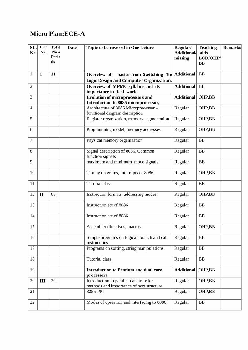
Micro Plan:ECE-A
SL.
No
Unit
No. Total
No.of
Perio
ds
Date Topic to be covered in One lecture Regular/
Additional/
missing
Teaching
aids used
LCD/OHP/
BB
Remarks
1 1 11 Overview of basics from Switching Theory & Logic Design and Computer Organization.
Additional BB
2 Overview of MPMC syllabus and its
importance in Real world
Additional BB
3 Evolution of microprocessors and
Introduction to 8085 microprocessor,
Additional OHP,BB
4 Architecture of 8086 Microprocessor –
functional diagram description
Regular OHP,BB
5 Register organization, memory segmentation Regular OHP,BB
6 Programming model, memory addresses Regular OHP,BB
7 Physical memory organization Regular BB
8 Signal description of 8086, Common
function signals
Regular BB
9 maximum and minimum mode signals Regular BB
10 Timing diagrams, Interrupts of 8086 Regular OHP,BB
11 Tutorial class Regular BB
12 II 08 Instruction formats, addressing modes Regular OHP,BB
13 Instruction set of 8086 Regular BB
14 Instruction set of 8086 Regular BB
15 Assembler directives, macros Regular OHP,BB
16 Simple programs on logical ,branch and call
instructions
Regular BB
17 Programs on sorting, string manipulations Regular BB
18 Tutorial class Regular BB
19 Introduction to Pentium and dual core
processors
Additional OHP,BB
20 III 20 Introduction to parallel data transfer
methods and importance of port structure
Regular OHP,BB
21 8255-PPI Regular OHP,BB
22 Modes of operation and interfacing to 8086 Regular BB
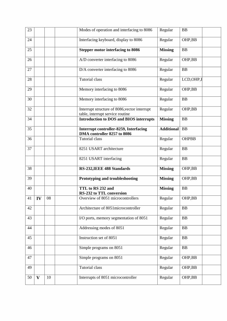
23 Modes of operation and interfacing to 8086 Regular BB
24 Interfacing keyboard, display to 8086 Regular OHP,BB
25 Stepper motor interfacing to 8086 Missing BB
26 A/D converter interfacing to 8086 Regular OHP,BB
27 D/A converter interfacing to 8086 Regular BB
28 Tutorial class Regular LCD,OHP,BB
29 Memory interfacing to 8086 Regular OHP,BB
30 Memory interfacing to 8086 Regular BB
32 Interrupt structure of 8086,vector interrupt
table, interrupt service routine
Regular OHP,BB
34 Introduction to DOS and BIOS interrupts Missing BB
35 Interrupt controller-8259, Interfacing
DMA controller 8257 to 8086
Additional BB
36 Tutorial class Regular OHPBB
37 8251 USART architecture Regular BB
8251 USART interfacing Regular BB
38 RS-232,IEEE 488 Standards Missing OHP,BB
39 Prototyping and troubleshooting Missing OHP,BB
40 TTL to RS 232 and
RS-232 to TTL conversion
Missing BB
41 IV 08 Overview of 8051 microcontrollers Regular OHP,BB
42 Architecture of 8051microcontroller Regular BB
43 I/O ports, memory segmentation of 8051 Regular BB
44 Addressing modes of 8051 Regular BB
45 Instruction set of 8051 Regular BB
46 Simple programs on 8051 Regular BB
47 Simple programs on 8051 Regular OHP,BB
49 Tutorial class Regular OHP,BB
50 V 10 Interrupts of 8051 microcontroller Regular OHP,BB
51 Timer/counters of 8051 Regular BB
52 Serial communication of 8051 Regular BB
53 Programming timer interrupts Regular OHP,BB
54 Programming external hardware interrupts Regular OHP,BB
55 Programming the serial communication
interrupts
Regular BB
56 Programming 8051 timers/counters Regular BB
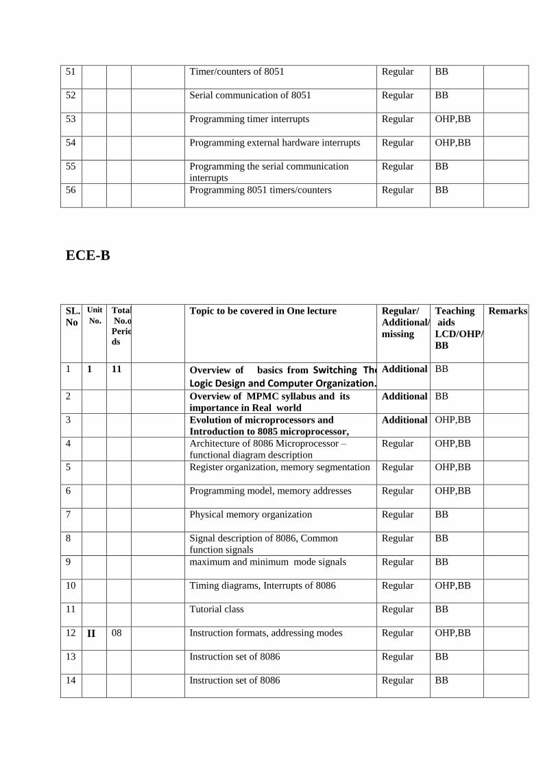
ECE-B
SL.
No
Unit
No. Total
No.of
Perio
ds
Topic to be covered in One lecture Regular/
Additional/
missing
Teaching
aids used
LCD/OHP/
BB
Remarks
1 1 11 Overview of basics from Switching Theory & Logic Design and Computer Organization.
Additional BB
2 Overview of MPMC syllabus and its
importance in Real world
Additional BB
3 Evolution of microprocessors and
Introduction to 8085 microprocessor,
Additional OHP,BB
4 Architecture of 8086 Microprocessor –
functional diagram description
Regular OHP,BB
5 Register organization, memory segmentation Regular OHP,BB
6 Programming model, memory addresses Regular OHP,BB
7 Physical memory organization Regular BB
8 Signal description of 8086, Common
function signals
Regular BB
9 maximum and minimum mode signals Regular BB
10 Timing diagrams, Interrupts of 8086 Regular OHP,BB
11 Tutorial class Regular BB
12 II 08 Instruction formats, addressing modes Regular OHP,BB
13 Instruction set of 8086 Regular BB
14 Instruction set of 8086 Regular BB

15 Assembler directives, macros Regular OHP,BB
16 Simple programs on logical ,branch and call
instructions
Regular BB
17 Programs on sorting, string manipulations Regular BB
18 Tutorial class Regular BB
19 Introduction to Pentium and dual core
processors
Additional OHP,BB
20 III 20 Introduction to parallel data transfer
methods and importance of port structure
Regular OHP,BB
21 8255-PPI Regular OHP,BB
22 Modes of operation and interfacing to 8086 Regular BB
23 Modes of operation and interfacing to 8086 Regular BB
24 Interfacing keyboard, display to 8086 Regular OHP,BB
25 Stepper motor interfacing to 8086 Missing BB
26 A/D converter interfacing to 8086 Regular OHP,BB
27 D/A converter interfacing to 8086 Regular BB
28 Tutorial class Regular LCD,OHP,BB
29 Memory interfacing to 8086 Regular OHP,BB
30 Memory interfacing to 8086 Regular BB
32 Interrupt structure of 8086,vector interrupt
table, interrupt service routine
Regular OHP,BB
34 Introduction to DOS and BIOS interrupts Missing BB
35 Interrupt controller-8259, Interfacing
DMA controller 8257 to 8086
Additional BB
36 Tutorial class Regular OHPBB
37 8251 USART architecture Regular BB
8251 USART interfacing Regular BB
38 RS-232,IEEE 488 Standards Missing OHP,BB
39 Prototyping and troubleshooting Missing OHP,BB
40 TTL to RS 232 and
RS-232 to TTL conversion
Missing BB
41 IV 08 Overview of 8051 microcontrollers Regular OHP,BB
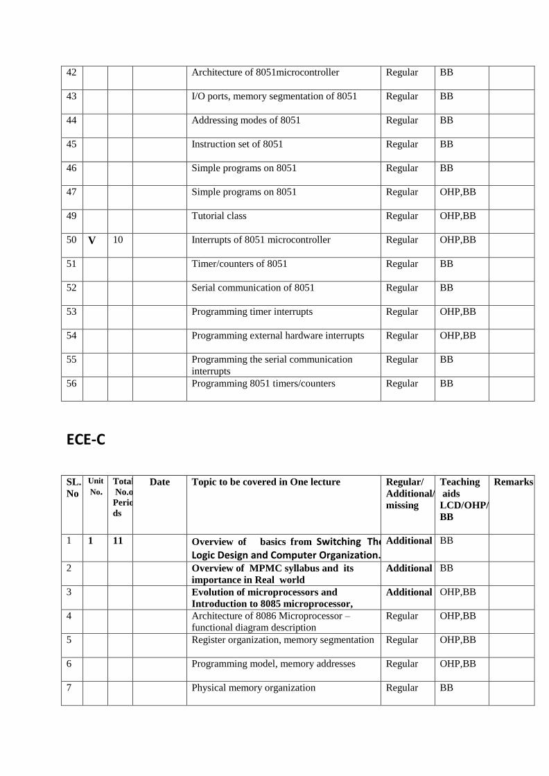
42 Architecture of 8051microcontroller Regular BB
43 I/O ports, memory segmentation of 8051 Regular BB
44 Addressing modes of 8051 Regular BB
45 Instruction set of 8051 Regular BB
46 Simple programs on 8051 Regular BB
47 Simple programs on 8051 Regular OHP,BB
49 Tutorial class Regular OHP,BB
50 V 10 Interrupts of 8051 microcontroller Regular OHP,BB
51 Timer/counters of 8051 Regular BB
52 Serial communication of 8051 Regular BB
53 Programming timer interrupts Regular OHP,BB
54 Programming external hardware interrupts Regular OHP,BB
55 Programming the serial communication
interrupts
Regular BB
56 Programming 8051 timers/counters Regular BB
ECE-C
SL.
No
Unit
No. Total
No.of
Perio
ds
Date Topic to be covered in One lecture Regular/
Additional/
missing
Teaching
aids used
LCD/OHP/
BB
Remarks
1 1 11 Overview of basics from Switching Theory & Logic Design and Computer Organization.
Additional BB
2 Overview of MPMC syllabus and its
importance in Real world
Additional BB
3 Evolution of microprocessors and
Introduction to 8085 microprocessor,
Additional OHP,BB
4 Architecture of 8086 Microprocessor –
functional diagram description
Regular OHP,BB
5 Register organization, memory segmentation Regular OHP,BB
6 Programming model, memory addresses Regular OHP,BB
7 Physical memory organization Regular BB
8 Signal description of 8086, Common
function signals
Regular BB
9 maximum and minimum mode signals Regular BB
10 Timing diagrams, Interrupts of 8086 Regular OHP,BB
11 Tutorial class Regular BB
12 II 08 Instruction formats, addressing modes Regular OHP,BB
13 Instruction set of 8086 Regular BB
14 Instruction set of 8086 Regular BB
15 Assembler directives, macros Regular OHP,BB
16 Simple programs on logical ,branch and call
instructions
Regular BB
17 Programs on sorting, string manipulations Regular BB
18 Tutorial class Regular BB
19 Introduction to Pentium and dual core
processors
Additional OHP,BB
20 III 20 Introduction to parallel data transfer
methods and importance of port structure
Regular OHP,BB
21 8255-PPI Regular OHP,BB
22 Modes of operation and interfacing to 8086 Regular BB
23 Modes of operation and interfacing to 8086 Regular BB
24 Interfacing keyboard, display to 8086 Regular OHP,BB
25 Stepper motor interfacing to 8086 Missing BB
26 A/D converter interfacing to 8086 Regular OHP,BB
27 D/A converter interfacing to 8086 Regular BB
28 Tutorial class Regular LCD,OHP,BB
29 Memory interfacing to 8086 Regular OHP,BB
30 Memory interfacing to 8086 Regular BB
32 Interrupt structure of 8086,vector interrupt
table, interrupt service routine
Regular OHP,BB
34 Introduction to DOS and BIOS interrupts Missing BB
35 Interrupt controller-8259, Interfacing
DMA controller 8257 to 8086
Additional BB
36 Tutorial class Regular OHPBB
37 8251 USART architecture Regular BB
8251 USART interfacing Regular BB
38 RS-232,IEEE 488 Standards Missing OHP,BB
39 Prototyping and troubleshooting Missing OHP,BB
40 TTL to RS 232 and
RS-232 to TTL conversion
Missing BB
41 IV 08 Overview of 8051 microcontrollers Regular OHP,BB
42 Architecture of 8051microcontroller Regular BB
43 I/O ports, memory segmentation of 8051 Regular BB
44 Addressing modes of 8051 Regular BB
45 Instruction set of 8051 Regular BB
46 Simple programs on 8051 Regular BB
47 Simple programs on 8051 Regular OHP,BB
49 Tutorial class Regular OHP,BB
50 V 10 Interrupts of 8051 microcontroller Regular OHP,BB
51 Timer/counters of 8051 Regular BB
52 Serial communication of 8051 Regular BB
53 Programming timer interrupts Regular OHP,BB
54 Programming external hardware interrupts Regular OHP,BB
55 Programming the serial communication
interrupts
Regular BB
56 Programming 8051 timers/counters Regular BB
ECE –D
SL.
No
Unit
No. Total
No.of Date Topic to be covered in One lecture Regular/
Additional/
Teaching
aids used
Remarks
Perio
ds missing LCD/OHP/
BB
1 1 11 Overview of basics from Switching Theory & Logic Design and Computer Organization.
Additional BB
2 Overview of MPMC syllabus and its
importance in Real world
Additional BB
3 Evolution of microprocessors and
Introduction to 8085 microprocessor,
Additional OHP,BB
4 Architecture of 8086 Microprocessor –
functional diagram description
Regular OHP,BB
5 Register organization, memory segmentation Regular OHP,BB
6 Programming model, memory addresses Regular OHP,BB
7 Physical memory organization Regular BB
8 Signal description of 8086, Common
function signals
Regular BB
9 maximum and minimum mode signals Regular BB
10 Timing diagrams, Interrupts of 8086 Regular OHP,BB
11 Tutorial class Regular BB
12 II 08 Instruction formats, addressing modes Regular OHP,BB
13 Instruction set of 8086 Regular BB
14 Instruction set of 8086 Regular BB
15 Assembler directives, macros Regular OHP,BB
16 Simple programs on logical ,branch and call
instructions
Regular BB
17 Programs on sorting, string manipulations Regular BB
18 Tutorial class Regular BB
19 Introduction to Pentium and dual core
processors
Additional OHP,BB
20 III 20 Introduction to parallel data transfer
methods and importance of port structure
Regular OHP,BB
21 8255-PPI Regular OHP,BB
22 Modes of operation and interfacing to 8086 Regular BB
23 Modes of operation and interfacing to 8086 Regular BB
24 Interfacing keyboard, display to 8086 Regular OHP,BB
25 Stepper motor interfacing to 8086 Missing BB
26 A/D converter interfacing to 8086 Regular OHP,BB
27 D/A converter interfacing to 8086 Regular BB
28 Tutorial class Regular LCD,OHP,BB
29 Memory interfacing to 8086 Regular OHP,BB
30 Memory interfacing to 8086 Regular BB
32 Interrupt structure of 8086,vector interrupt
table, interrupt service routine
Regular OHP,BB
34 Introduction to DOS and BIOS interrupts Missing BB
35 Interrupt controller-8259, Interfacing
DMA controller 8257 to 8086
Additional BB
36 Tutorial class Regular OHPBB
37 8251 USART architecture Regular BB
8251 USART interfacing Regular BB
38 RS-232,IEEE 488 Standards Missing OHP,BB
39 Prototyping and troubleshooting Missing OHP,BB
40 TTL to RS 232 and
RS-232 to TTL conversion
Missing BB
41 IV 08 Overview of 8051 microcontrollers Regular OHP,BB
42 Architecture of 8051microcontroller Regular BB
43 I/O ports, memory segmentation of 8051 Regular BB
44 Addressing modes of 8051 Regular BB
45 Instruction set of 8051 Regular BB
46 Simple programs on 8051 Regular BB
47 Simple programs on 8051 Regular OHP,BB
49 Tutorial class Regular OHP,BB
50 V 10 Interrupts of 8051 microcontroller Regular OHP,BB
51 Timer/counters of 8051 Regular BB
52 Serial communication of 8051 Regular BB
53 Programming timer interrupts Regular OHP,BB
54 Programming external hardware interrupts Regular OHP,BB
55 Programming the serial communication
interrupts
Regular BB
56 Programming 8051 timers/counters Regular BB
14.Detailed notes
UNIT-I
8085 Microprocessor Contents
•General definitions
•Overview of 8085 microprocessor
•Overview of 8086 microprocessor
•Signals and pins of 8086 microprocessor
The salient features of 8085 µp are:
•It is a 8 bit microprocessor.
•It is manufactured with N-MOS technology.
•It has 16-bit address bus and hence can address up to 216 =65536 bytes (64KB) memory locations through A0-A15.
•The first 8 lines of address bus and 8 lines of data bus are multiplexed AD0 – AD7. •Data bus is a group of 8 lines D0 – D7.
•It supports external interrupt request.
•A 16 bit program counter (PC)
•A 16 bit stack pointer (SP)
•Six 8-bit general purpose register arranged in pairs: BC, DE, HL.
•It requires a signal +5V power supply and operates at 3.2 MHZ single phase clock. •It is enclosed with 40 pins DIP (Dual in line package).
Overview of 8085 microprocessor
8085 Architecture
• Pin Diagram
• Functional Block Diagram
Instruction Set
8085 instruction set consists of the following instructions:
Data moving instructions.
Arithmetic - add, subtract, increment and decrement.
Logic - AND, OR, XOR and rotate.
Control transfer - conditional, unconditional, call subroutine, return from
subroutine and restarts.
Input/Output instructions.
Other - setting/clearing flag bits, enabling/disabling interrupts, stack operations,
etc.
Addressing mode
•Register - references the data in a register or in a register pair.
Register indirect - instruction specifies register pair containing address, where the data is located.
Direct, Immediate - 8 or 16-bit data.
Advantages of 8086 over 8085 are:
1. pipelining is employed making the execution faster.
2. data bus width increased to 16 bits.
3. higher memory of 1MB.
4. some instructions such as MUL or DIV are available for multiplication and division.
5. increased instruction set making the programming easier.
•EU executes instructions from the instruction system byte queue.
•Both units operate asynchronously to give the 8086 an overlapping instruction fetch and execution mechanism which is called as Pipelining. This results in efficient use of the system bus and system performance.
•BIU contains Instruction queue, Segment registers, Instruction pointer, Address adder.
•EU contains Control circuitry, Instruction decoder, ALU, Pointer and Index register, Flag register.
BUS INTERFACR UNIT:
• It provides a full 16 bit bidirectional data bus and 20 bit address bus.
•The bus interface unit is responsible for performing all external bus operations.
Specifically it has the following functions:
•Instruction fetch, Instruction queuing, Operand fetch and storage, Address relocation
and Bus control.
•The BIU uses a mechanism known as an instruction stream queue to implement a
pipeline architecture.
•This queue permits prefetch of up to six bytes of instruction code. When ever the queue
of the BIU is not full, it has room for at least two more bytes and at the same time the EU
is not requesting it to read or write operands from memory, the BIU is free to look
ahead in the program by prefetching the next sequential instruction.
•These prefetching instructions are held in its FIFO queue. With its 16 bit data bus, the
BIU fetches two instruction bytes in a single memory cycle.
•After a byte is loaded at the input end of the queue, it automatically shifts up through
the FIFO to the empty location nearest the output.
•The EU accesses the queue from the output end. It reads one instruction byte after the
other from the output of the queue. If the queue is full and the EU is not requesting
access to operand in memory.
•These intervals of no bus activity, which may occur between bus cycles are known as
Idle state.
•If the BIU is already in the process of fetching an instruction when the EU request it to
read or write operands from memory or I/O, the BIU first completes the instruction
fetch bus cycle before initiating the operand read / write cycle.
•The BIU also contains a dedicated adder which is used to generate the 20bit physical
address that is output on the address bus. This address is formed med by combining the
current contents of the code segment CS register and the current contents of the
instruction pointer IP register.
•The BIU is also responsible for generating bus control signals such as those for memory
read or write and I/O read or write.
EXECUTION UNIT
The Execution unit is responsible for decoding and executing all instructions.
•The EU extracts instructions from the top of the queue in the BIU, decodes them,
generates operands if necessary, passes them to the BIU and requests it to perform the
read or write bys cycles to memory or I/O and perform the operation specified by the
instruction on the operands.
•During the execution of the instruction, the EU tests the status and control flags and
updates them based on the results of executing the instruction.
•If the queue is empty, the EU waits for the next instruction byte to be fetched and
shifted to top of the queue.
•When the EU executes a branch or jump instruction, it transfers control to a location
corresponding to another set of sequential instructions.
SPECIAL FUNCTIONS OF GENERAL PURPOSE REGISTERS
Accumulator register consists of 2 8-bit registers AL and AH, which can be combined
together and used as a 16-bit register AX. AL in this case contains the low-order byte of
the word, and AH contains the high-order byte. Accumulator can be used for I/O
operations and string manipulation.
Base register consists of 2 8-bit registers BL and BH, which can be combined together
and used as a 16-bit register BX. BL in this case contains the low-order byte of the word,
and BH contains the high-order byte. BX register usually contains a data pointer used
for based, based indexed or register indirect addressing.
Count register consists of 2 8-bit registers CL and CH, which can be combined together
and used as a 16-bit register CX. When combined, CL register contains the low-order
byte of the word, and CH contains the high-order byte. Count register can be used as a
counter in string manipulation and shift/rotate instructions.
Data register consists of 2 8-bit registers DL and DH, which can be combined together
and used as a 16-bit register DX. When combined, DL register contains the low-order
byte of the word, and DH contains the high-order byte. Data register can be used as a
port number in I/O operations. In integer 32-bit multiply and divide instruction the DX
register contains high-order word of the initial or resulting number.
SPECIAL FUNCTIONS OF SPECIAL PURPOSE REGISTERS
Stack Pointer (SP) is a 16-bit register pointing to program stack.
Base Pointer (BP) is a 16-bit register pointing to data in stack segment. BP register is
usually used for based, based indexed or register indirect addressing.
Source Index (SI) is a 16-bit register. SI is used for indexed, based indexed and register
indirect addressing, as well as a source data address in string manipulation
instructions.
Destination Index (DI) is a 16-bit register. DI is used for indexed, based indexed and
register indirect addressing, as well as a destination data address in string
manipulation instructions. The si and di registers (Source Index and Destination Index
) have some special purposes as well. You may use these registers as pointers (much
like the bx register) to indirectly access memory. You'll also use these registers with
the 8086 string instructions when processing character strings.
The bp register (Base Pointer) is similar to the bx register. You'll generally use this
register to access parameters and local variables in a procedure.
The sp register (Stack Pointer) has a very special purpose - it maintains the program
stack. Normally, you would not use this register for arithmetic computations. The
proper operation of most programs depends upon the careful use of this register.
SEGMENTATION:
Since address registers and address operands are only 16 bits they can only address 64k
bytes. In order toaddress the 20-bit address range of the 8086, physicaladdresses (those
that are put on the address bus)are always formed by adding the values of one of the
instruction is executed? The use of segment registers reduces the size ofpointers to 16
bits.
This reduces the code size but also restricts the addressing range of a pointer to 64k
bytes. Performing address arithmetic within data structures larger than 64k is
awkward. This is the biggest drawback of the 8086 architecture. We will restrict
ourslves to short programs where all of the code, data and stack are placed into thesame
64k segment (i.e. CS=DS=SS).
Most of the registers contain data/instruction offsets within 64 KB memory segment.
There are four different 64 KB segments for instructions, stack, data and extra data. To
specify where in 1 MB of processor memory these 4 segments are located the
processor uses four segment registers:
Memory
•Program, data and stack memories occupy the same memory space. As the most of the
processor instructions use 16-bit pointers the processor can effectively address only 64
KB of memory.
• To access memory outside of 64 KB the CPU uses special segment registers to specify
where the code, stack and data 64 KB segments are positioned within 1 MB of memory
(see the "Registers" section below).
•16-bit pointers and data are stored as:
address: low-order byte
address+1: high-order byte
•Program memory - program can be located anywhere in memory. Jump and call
instructions can be used for short jumps within currently selected 64 KB code segment,
as well as for far jumps anywhere within 1 MB of memory.
•All conditional jump instructions can be used to jump within approximately +127 to -
127 bytes from current instruction.
•Data memory - the processor can access data in any one out of 4 available segments,
which limits the size of accessible memory to 256 KB (if all four segments point to
different 64 KB blocks).
•Accessing data from the Data, Code, Stack or Extra segments can be usually done by
prefixing instructions with the DS:, CS:, SS: or ES: (some registers and instructions by
default may use the ES or SS segments instead of DS segment).
•Word data can be located at odd or even byte boundaries. The processor uses two
memory accesses to read 16-bit word located at odd byte boundaries. Reading word
data from even byte boundaries requires only one memory access.
•Stack memory can be placed anywhere in memory. The stack can be located at odd
memory addresses, but it is not recommended for performance reasons (see "Data
Memory" above).
Reserved locations:
•0000h - 03FFh are reserved for interrupt vectors. Each interrupt vector is a 32-bit
pointer in format segment: offset.
•FFFF0h - FFFFFh - after RESET the processor always starts program execution at the
FFFF0h address.
segment registers to the 16-bit address to form a 20-bit address.
The segment registers themselves only contain themost-significant 16 bits of the 20-bit
value that iscontributed by the segment registers. The least significantfour bits of
thesegment address are alwayszero.
By default, the DS (data segment) is used fordata transfer instructions (e.g. MOV),
CS(codesegment) is used with control transfer instructions(e.g. JMP or CALL), and SS is
used with the stackpointer (e.g. PUSH or to save/restore addresses duringCALL/RET or
INT instructions).
Exercise: If DS contains 0100H, what address will be written by the instruction MOV
[2000H],AL? If CX contains 1122H, SP contains 1234H, and SS contains 2000H, what
memory values will change and what will be their values when the PUSH CX
Code segment (CS) is a 16-bit register containing address of 64 KB segment with
processor instructions. The processor uses CS segment for all accesses to instructions
referenced by instruction pointer (IP) register. CS register cannot be changed directly.
The CS register is automatically updated during far jump, far call and far return
instructions.
Stack segment (SS) is a 16-bit register containing address of 64KB segment with
program stack. By default, the processor assumes that all data referenced by the stack
pointer (SP) and base pointer (BP) registers is located in the stack segment. SS register
can be changed directly using POP instruction.
Data segment (DS) is a 16-bit register containing address of 64KB segment with
program data. By default, the processor assumes that all data referenced by general
registers (AX, BX, CX, DX) and index register (SI, DI) is located in the data segment. DS
register can be changed directly using POP and LDS instructions.
Extra segment (ES) is a 16-bit register containing address of 64KB segment, usually
with program data. By default, the processor assumes that the DI register references
the ES segment in string manipulation instructions. ES register can be changed directly
using POP and LES instructions.
It is possible to change default segments used by general and index registers by
prefixing instructions with a CS, SS, DS or ES prefix.
8086 FLAG REGISTER
Flags is a 16-bit register containing 9 1-bit flags:
Overflow Flag (OF) - set if the result is too large positive number, or is too small
negative number to fit into destination operand.
Direction Flag (DF) - if set then string manipulation instructions will auto-
decrement index registers. If cleared then the index registers will be auto-
incremented.
Interrupt-enable Flag (IF) - setting this bit enables maskable interrupts.
Single-step Flag (TF) - if set then single-step interrupt will occur after the next
instruction.
Sign Flag (SF) - set if the most significant bit of the result is set.
Zero Flag (ZF) - set if the result is zero.
Auxiliary carry Flag (AF) - set if there was a carry from or borrow to bits 0-3 in
the AL register.
Parity Flag (PF) - set if parity (the number of "1" bits) in the low-order byte of the
result is even.
Carry Flag (CF) - set if there was a carry from or borrow to the most significant bit
during last result calculation
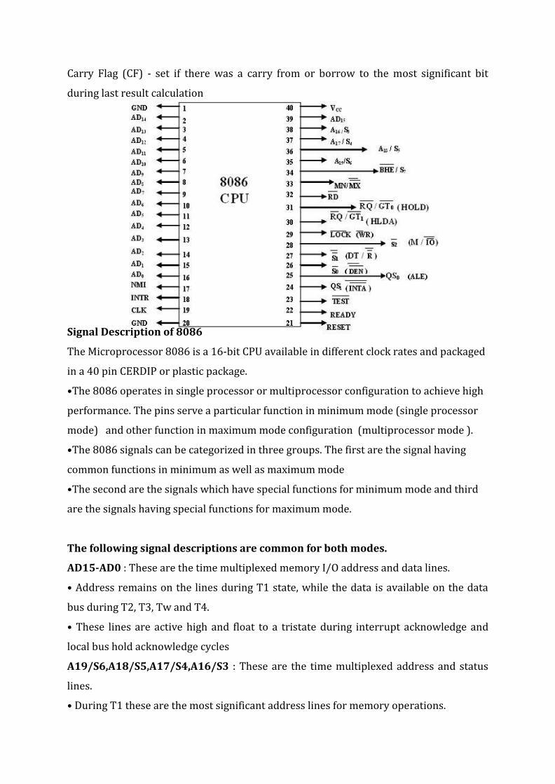
Signal Description of 8086
The Microprocessor 8086 is a 16-bit CPU available in different clock rates and packaged
in a 40 pin CERDIP or plastic package.
•The 8086 operates in single processor or multiprocessor configuration to achieve high
performance. The pins serve a particular function in minimum mode (single processor
mode) and other function in maximum mode configuration (multiprocessor mode ).
•The 8086 signals can be categorized in three groups. The first are the signal having
common functions in minimum as well as maximum mode
•The second are the signals which have special functions for minimum mode and third
are the signals having special functions for maximum mode.
The following signal descriptions are common for both modes.
AD15-AD0 : These are the time multiplexed memory I/O address and data lines.
• Address remains on the lines during T1 state, while the data is available on the data
bus during T2, T3, Tw and T4.
• These lines are active high and float to a tristate during interrupt acknowledge and
local bus hold acknowledge cycles
A19/S6,A18/S5,A17/S4,A16/S3 : These are the time multiplexed address and status
lines.
• During T1 these are the most significant address lines for memory operations.
•During I/O operations, these lines are low. During memory or I/O operations, status
information is available on those lines for T2,T3,Tw and T4.
• The status of the interrupt enable flag bit is updated at the beginning of each clock
cycle.
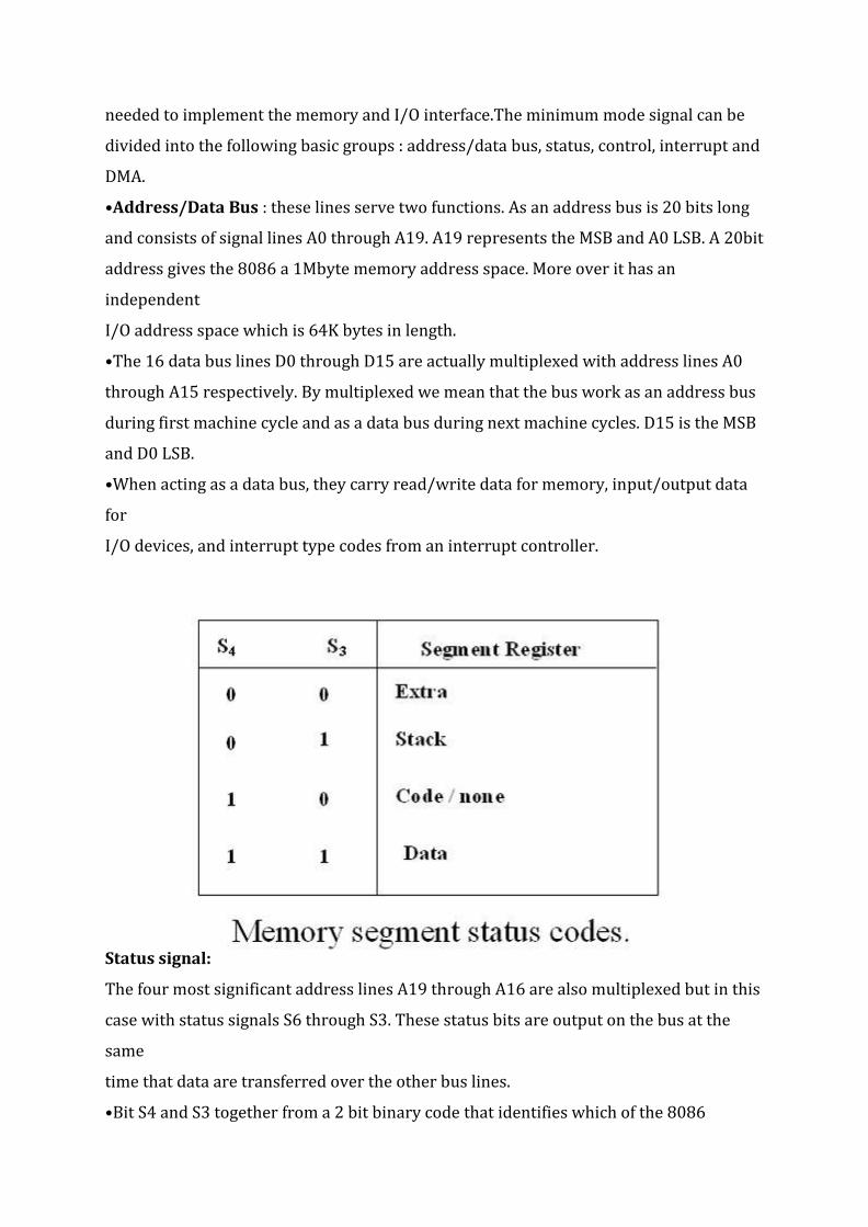
•The S4 and S3 combinedly indicate which segment register is presently being used for
memory accesses as in below fig.
•These lines float to tri-state off during the local bus hold acknowledge. The status line
S6 is always low .
•The address bit are separated from the status bit using latches controlled by the ALE
signal.
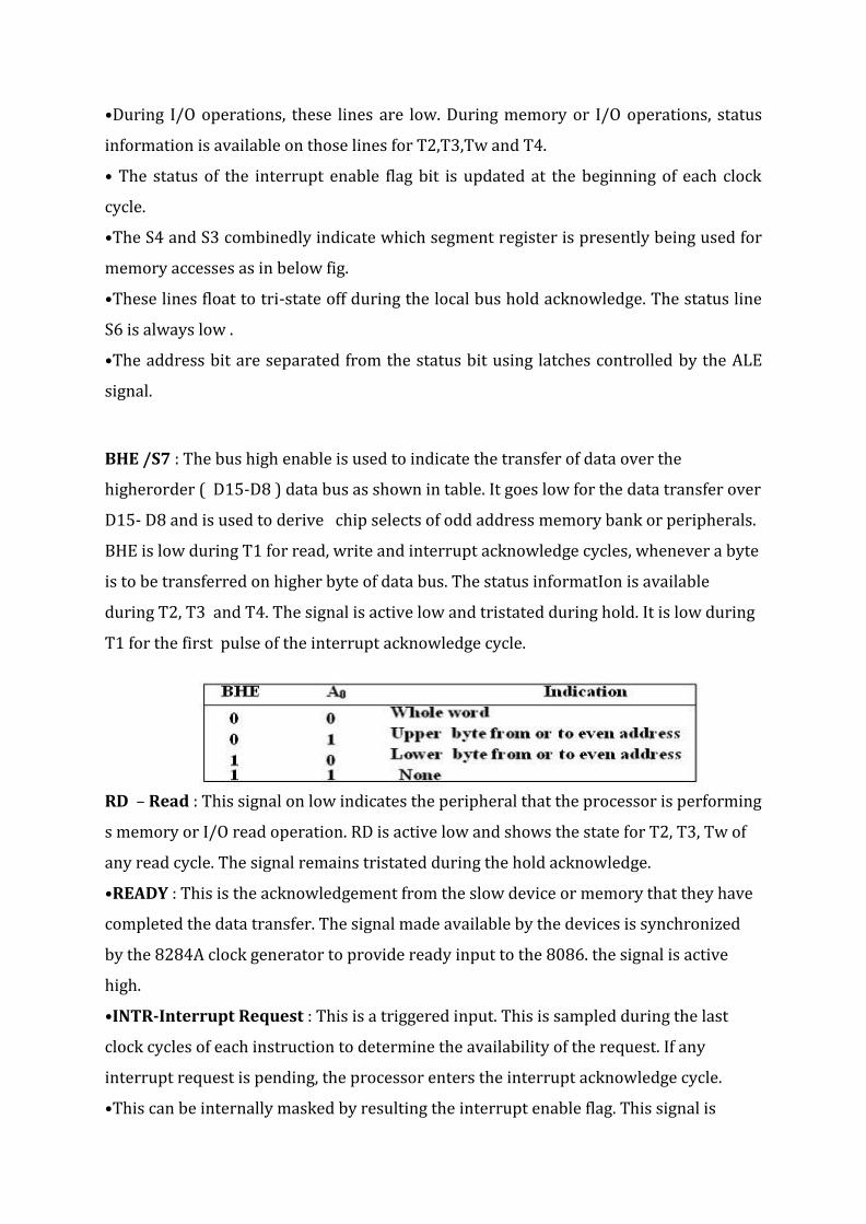
BHE /S7 : The bus high enable is used to indicate the transfer of data over the
higherorder ( D15-D8 ) data bus as shown in table. It goes low for the data transfer over
D15- D8 and is used to derive chip selects of odd address memory bank or peripherals.
BHE is low during T1 for read, write and interrupt acknowledge cycles, whenever a byte
is to be transferred on higher byte of data bus. The status informatIon is available
during T2, T3 and T4. The signal is active low and tristated during hold. It is low during
T1 for the first pulse of the interrupt acknowledge cycle.
RD – Read : This signal on low indicates the peripheral that the processor is performing
s memory or I/O read operation. RD is active low and shows the state for T2, T3, Tw of
any read cycle. The signal remains tristated during the hold acknowledge.
•READY : This is the acknowledgement from the slow device or memory that they have
completed the data transfer. The signal made available by the devices is synchronized
by the 8284A clock generator to provide ready input to the 8086. the signal is active
high.
•INTR-Interrupt Request : This is a triggered input. This is sampled during the last
clock cycles of each instruction to determine the availability of the request. If any
interrupt request is pending, the processor enters the interrupt acknowledge cycle.
•This can be internally masked by resulting the interrupt enable flag. This signal is
active high and internally synchronized.
• TEST : This input is examined by a ‘WAIT’ instruction. If the TEST pin goes low,
execution will continue, else the processor remains in an idle state. The input is
synchronized internally during each clock cycle on leading edge of clock.
•CLK- Clock Input : The clock input provides the basic timing for processor operation
and bus control activity. Its an asymmetric square wave with 33% duty cycle
MN/ MX : The logic level at this pin decides whether the processor is to operate in
either minimum or maximum mode.
•The following pin functions are for the minimum mode operation of 8086.
•M/ IO – Memory/IO : This is a status line logically equivalent to S2 in maximum
mode. When it is low, it indicates the CPU is having an I/O operation, and when it is
high, it indicates that the CPU is having a memory operation. This line Becomes active
high in the previous T4 and remains active till final T4 of the current cycle. It is tri stated
during local bus “hold acknowledge “.
INTA – Interrupt Acknowledge : This signal is used as a read strobe for interrupt
acknowledge cycles. i.e. when it goes low, the processor has accepted the interrupt.
ALE – Address Latch Enable :This output signal indicates the availability of the valid
address on the address/data lines, and is connected to latch enable input of latches. This
signal is active high and is never tri stated.
•DT/ R – Data Transmit/Receive: This output is used to decide the direction of data
flow through the transceivers (bidirectional buffers). When the processor sends out
data, this signal is high and when the processor is receiving data, this signal is low.
•DEN – Data Enable :This signal indicates the availability of valid data over the
address/data lines. It is used to enable the transceivers ( bi directional buffers ) to
separate the data from the multiplexed address/data signal. It is active from the middle
of T2 until the middle of T4. This is tri stated during hold acknowledge’ cycle.
HOLD, HLDA- Acknowledge : When the HOLD line goes high, it indicates to the
processor that another master is requesting the bus access.•The processor, after
receiving the HOLD request, issues the hold acknowledge signal on HLDA pin, in the
middle of the next clock cycle after completing the current bus cycle.•At the same time,
the processor floats the local bus and control lines. When the processor detects the
HOLD line low, it lowers the HLDA signal. HOLD is an asynchronous input, and is should
be externally synchronized.•If the DMA request is made while the CPU is performing a
memory or I/O cycle, it will release the local bus during T4 provided :
1.The request occurs on or before T2 state of the current cycle.
2.The current cycle is not operating over the lower byte of a word.
3.The current cycle is not the first acknowledge of an interrupt acknowledge sequence.
4. A Lock instruction is not being executed
The following pin function are applicable for maximum mode operation of 8086.
•S2, S1, S0 – Status Lines : These are the status lines which reflect the type of
operation, being carried out by the processor. These become activity during T4 of the
previous cycle and active during T1 and T2 of the current bus cycles.
LOCK: This output pin indicates that other system bus master will be prevented from
gaining the system bus, while the LOCK signal is low
•The LOCK signal is activated by the ‘LOCK’ prefix instruction and remains active until
the completion of the next instruction. When the CPU is executing a critical instruction
which requires the system bus, the LOCK prefix instruction ensures that other
processors connected in the system will not gain the control of the bus.
• The 8086, while executing the prefixed instruction, asserts the bus lock signal output,
which may be connected to an external bus controller.
•QS1, QS0 – Queue Status: These lines give information about the status of the code-
prefetch queue. These are active during the CLK cycle after while the queue operation is
performed.
•This modification in a simple fetch and execute architecture of a conventional
microprocessor offers an added advantage of pipelined processing of the instructions.
•The 8086 architecture has 6-byte instruction prefetch queue. Thus even the largest (6-
bytes) instruction can be prefetched from the memory and stored in the prefetch. This
results in a faster execution of the instructions.
•In 8085 an instruction is fetched, decoded and executed and only after the execution of
this instruction, the next one is fetched.
•By prefetching the instruction, there is a considerable speeding up in instruction
execution in 8086. This is known as instruction pipelining.
•At the starting the CS:IP is loaded with the required address from which the execution
is to be started. Initially, the queue will be empty an the microprocessor starts a fetch
operation to bring one byte (the first byte) of instruction code, if the CS:IP address is
odd or two bytes at a time, if the CS:IP address is even.
•The first byte is a complete opcode in case of some instruction (one byte opcode
instruction) and is a part of opcode, in case of some instructions ( two byte opcode
instructions), the remaining part of code lie in second byte.
•The second byte is then decoded in continuation with the first byte to decide the
instruction length and the number of subsequent bytes to be treated as instruction data.
•The queue is updated after every byte is read from the queue but the fetch cycle is
initiated by BIU only if at least two bytes of the queue are empty and the EU may be
concurrently executing the fetched instructions
• RQ / GT0 , RQ / GT1 – Request/Grant : These pins are used by the other local bus
master in maximum mode, to force the processor to release the local bus at the end of
the processor current bus cycle.
•Each of the pin is bidirectional with RQ/GT0 having higher priority than RQ/GT1.
•RQ/GT pins have internal pull-up resistors and may be left unconnected.
Request/Grant sequence is as follows:
1.A pulse of one clock wide from another bus master requests the bus access to 8086.
2.During T4(current) or T1(next) clock cycle, a pulse one clock wide from 8086 to the
requesting master, indicates that the 8086 has allowed the local bus to float and that it
will enter the ‘hold acknowledge’ state at next cycle. The CPU bus interface unit is likely
to be disconnected from the local bus of the system.
3.A one clock wide pulse from the another master indicates to the 8086 that the hold
request is about to end and the 8086 may regain control of the local bus at the next
clock cycle. Thus each master to master exchange of the local bus is a sequence of 3
pulses. There must be at least one dead clock cycle after each bus exchange.
•The request and grant pulses are active low.
•For the bus request those are received while 8086 is performing memory or I/O cycle,
the granting of the bus is governed by the rules as in case of HOLD and HLDA in
minimum mode.
General Bus Operation:
•The 8086 has a combined address and data bus commonly referred as a time
multiplexed address and data bus.
• The main reason behind multiplexing address and data over the same pins is the
maximum utilization of processor pins and it facilitates the use of 40 pin standard DIP
package. Maximum utilization of processor pins and it facilitates the use of 40 pin
standard DIP package.
•The bus can be de multiplexed using a few latches and transceivers, when ever
required.
•Basically, all the processor bus cycles consist of at least four clock cycles. These are
refered to as T1, T2, T3, T4. The address is transmitted by the processor during T1. It is
present on the bus only for one cycle.
•The negative edge of this ALE pulse is used to separate the address and the data or
status
information. In maximum mode, the status lines S0, S1 and S2 are used to indicate the
type of operation.
•In a minimum mode 8086 system, the microprocessor 8086 is operated in minimum
mode by strapping its MN/MX pin to logic 1.
•In this mode, all the control signals are given out by the microprocessor chip itself. There is a single microprocessor in the minimum mode system.
•The remaining components in the system are latches, transreceivers, clock generator, memory and I/O devices. Some type of chip selection logic may be required for selecting memory or I/O devices, depending upon the address map of the system.
•Latches are generally buffered output D-type flip-flops like 74LS373 or 8282. They are used for separating the valid address from the multiplexed address/data signals and arecontrolled by the ALE signal generated by 8086.
•Transreceivers are the bidirectional buffers and some times they are called as data
amplifiers. They are required to separate the valid data from the time multiplexed
address/data signals.
•They are controlled by two signals namely, DEN and DT/R The DEN signal indicates the
direction of data, i.e. from or to the processor. The system contains memory for the
monitor and users program storage.
•Usually, EPROM are used for monitor storage, while RAM for users program storage. A
system may contain I/O devices.
•The working of the minimum mode configuration system can be better described in
terms of the timing diagrams rather than qualitatively describing the operations.
•The opcode fetch and read cycles are similar. Hence the timing diagram can be
categorized in two parts, the first is the timing diagram for read cycle and the second is
the timing diagram for write cycle.
•The read cycle begins in T1 with the assertion of address latch enable (ALE) signal and
also M / IO signal. During the negative going edge of this signal, the valid address is
latched on the local bus.
•The BHE and A0 signals address low, high or both bytes. From T1 to T4 , the M/IO
signal indicates a memory or I/O operation.
•At T2, the address is removed from the local bus and is sent to the output. The bus is
then tristated. The read (RD) control signal is also activated in T2.
•The read (RD) signal causes the address device to enable its data bus drivers. After RD
goes low, the valid data is available on the data bus.
•The addressed device will drive the READY line high. When the processor returns the
read signal to high level, the addressed device will again tristate its bus drivers.
•A write cycle also begins with the assertion of ALE and the emission of the address. The
M/IO signal is again asserted to indicate a memory or I/O operation. In T2, after sending
the address in T1, the processor sends the data to be written to the addressed location.
•The data remains on the bus until middle of T4 state. The WR becomes active at the
beginning of T2 (unlike RD is somewhat delayed in T2 to provide time for floating).
•The BHE and A0 signals are used to select the proper byte or bytes of memory or I/O
word to be read or write.
•The M/IO, RD and WR signals indicate the type of data transfer as specified in table
below.
Hold Response sequence: The HOLD pin is checked at leading edge of each clock pulse.
If it is received active by the processor before T4 of the previous cycle or during T1 state
of the current cycle, the CPU activates HLDA in the next clock cycle and for succeeding
bus cycles, the bus will be given to another requesting master.
•The control of the bus is not regained by the processor until the requesting master
does not drop the HOLD pin low. When the request is dropped by the requesting master,
the HLDA is dropped by the processor at the trailing edge of the next clock.
Maximum Mode 8086 System
•In the maximum mode, the 8086 is operated by strapping the MN/MX pin to ground.
•In this mode, the processor derives the status signal S2, S1, S0. Another chip called bus
controller derives the control signal using this status information .
•In the maximum mode, there may be more than one microprocessor in the system
configuration.
•The components in the system are same as in the minimum mode system.
•The basic function of the bus controller chip IC8288, is to derive control signals like RD
and WR ( for memory and I/O devices), DEN, DT/R, ALE etc. using the information by
the processor on the status lines.
•The bus controller chip has input lines S2, S1, S0 and CLK. These inputs to 8288 are
driven by CPU.
•It derives the outputs ALE, DEN, DT/R, MRDC, MWTC, AMWC, IORC, IOWC and AIOWC.
The AEN, IOB and CEN pins are specially useful for multiprocessor systems.
•AEN and IOB are generally grounded. CEN pin is usually tied to +5V. The significance
of the MCE/PDEN output depends upon the status of the IOB pin.
•If IOB is grounded, it acts as master cascade enable to control cascade 8259A, else it
acts as peripheral data enable used in the multiple bus configurations.
•INTA pin used to issue two interrupt acknowledge pulses to the interrupt controller or
to an interrupting device
IORC, IOWC are I/O read command and I/O write command signals respectively .These
signals enable an IO interface to read or write the data from or to the address port.
•The MRDC, MWTC are memory read command and memory write command signals
respectively and may be used as memory read or write signals.
•All these command signals instructs the memory to accept or send data from or to the
bus.
•For both of these write command signals, the advanced signals namely AIOWC and
AMWTC are available.
•Here the only difference between in timing diagram between minimum mode and
maximum mode is the status signals used and the available control and advanced
command signals.
•R0, S1, S2 are set at the beginning of bus cycle.8288 bus controller will output a pulse as on the ALE and apply a required signal to its DT / R pin during T1.
•In T2, 8288 will set DEN=1 thus enabling transceivers, and for an input it will activate
MRDC or IORC. These signals are activated until T4. For an output, the AMWC or AIOWC
is activated from T2 to T4 and MWTC or IOWC is activated from T3 to T4.
•The status bit S0 to S2 remains active until T3 and become passive during T3 and T4.
•If reader input is not activated before T3, wait state will be inserted between T3 and
T4.
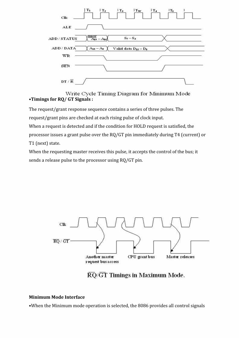
•Timings for RQ/ GT Signals :
The request/grant response sequence contains a series of three pulses. The
request/grant pins are checked at each rising pulse of clock input.
When a request is detected and if the condition for HOLD request is satisfied, the
processor issues a grant pulse over the RQ/GT pin immediately during T4 (current) or
T1 (next) state.
When the requesting master receives this pulse, it accepts the control of the bus; it
sends a release pulse to the processor using RQ/GT pin.
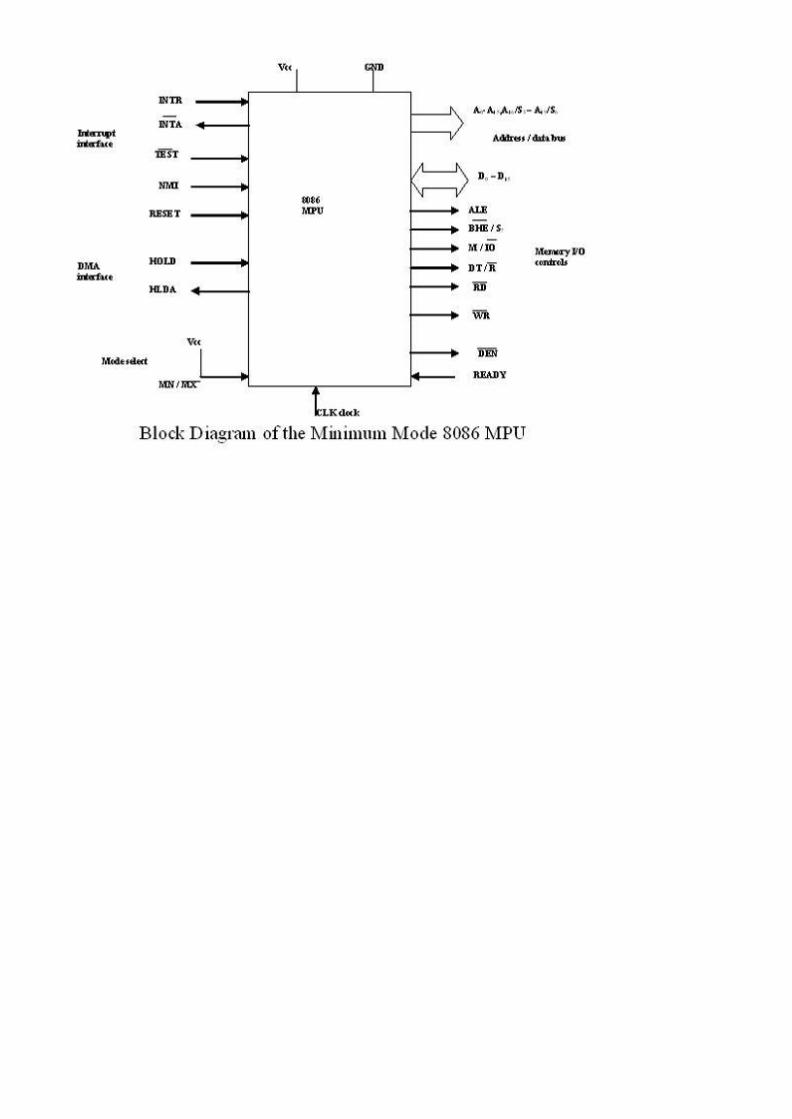
Minimum Mode Interface
•When the Minimum mode operation is selected, the 8086 provides all control signals
needed to implement the memory and I/O interface.The minimum mode signal can be
divided into the following basic groups : address/data bus, status, control, interrupt and
DMA.
•Address/Data Bus : these lines serve two functions. As an address bus is 20 bits long
and consists of signal lines A0 through A19. A19 represents the MSB and A0 LSB. A 20bit
address gives the 8086 a 1Mbyte memory address space. More over it has an
independent
I/O address space which is 64K bytes in length.
•The 16 data bus lines D0 through D15 are actually multiplexed with address lines A0
through A15 respectively. By multiplexed we mean that the bus work as an address bus
during first machine cycle and as a data bus during next machine cycles. D15 is the MSB
and D0 LSB.
•When acting as a data bus, they carry read/write data for memory, input/output data
for
I/O devices, and interrupt type codes from an interrupt controller.
Status signal:
The four most significant address lines A19 through A16 are also multiplexed but in this
case with status signals S6 through S3. These status bits are output on the bus at the
same
time that data are transferred over the other bus lines.
•Bit S4 and S3 together from a 2 bit binary code that identifies which of the 8086
internal
segment registers are used to generate the physical address that was output on the
address
bus during the current bus cycle.
•Code S4S3 = 00 identifies a register known as extra segment register as the source of
the segment address.
•Status line S5 reflects the status of another internal characteristic of the 8086. It is the
logic level of the internal enable flag. The last status bit S6 is always at the logic 0 level
•Control Signals :
The control signals are provided to support the 8086 memory I/O interfaces. They
control functions such as when the bus is to carry a valid address in which direction
data
are to be transferred over the bus, when valid write data are on the bus and when to put
read data on the system bus.
ALE is a pulse to logic 1 that signals external circuitry when a valid address word is on
the bus. This address must be latched in external circuitry on the 1-to-0 edge of the
pulse
•Another control signal that is produced during the bus cycle is BHE bank high enable.
Logic 0 on this used as a memory enable signal for the most significant byte half of the
data bus D8 through D1. These lines also serves a second function, which is as the S7
status line.
•Using the M/IO and DT/R lines, the 8086 signals which type of bus cycle is in progress
and in which direction data are to be transferred over the bus.
•The logic level of M/IO tells external circuitry whether a memory or I/O transfer is
taking place over the bus. Logic 1 at this output signals a memory operation and logic 0
an I/O operation.
•The direction of data transfer over the bus is signaled by the logic level output at DT/R.
When this line is logic 1 during the data transfer part of a bus cycle, the bus is in the
transmit mode. Therefore, data are either written into memory or output to an I/O
device.
•On the other hand, logic 0 at DT/R signals that the bus is in the receive mode. This
corresponds to reading data from memory or input of data from an input port.
•The signal read RD and write WR indicates that a read bus cycle or a write bus cycle is
in progress. The 8086 switches WR to logic 0 to signal external device that valid write or
output data are on the bus
• On the other hand, RD indicates that the 8086 is performing a read of data of the bus.
During read operations, one other control signal is also supplied. This is DEN ( data
enable) and it signals external devices when they should put data on the bus.
•There is one other control signal that is involved with the memory and I/O interface.
This is the READY signal.
•READY signal is used to insert wait states into the bus cycle such that it is extended by
a number of clock periods. This signal is provided by an external clock generator device
and can be supplied by the memory or I/O sub-system to signal the 8086 when they are
ready to permit the data transfer to be completed
Maximum Mode Interface
•When the 8086 is set for the maximum-mode configuration, it provides signals for
implementing a multiprocessor / coprocessor system environment.
•By multiprocessor environment we mean that one microprocessor exists in the system
and that each processor is executing its own program.
• Usually in this type of system environment, there are some system resources that are
common to all processors.
•They are called as global resources. There are also other resources that are assigned
to
specific processors. These are known as local or private resources.
•Coprocessor also means that there is a second processor in the system. In this two
processor does not access the bus at the same time.
•One passes the control of the system bus to the other and then may suspend its
operation.
•In the maximum-mode 8086 system, facilities are provided for implementing allocation
of global resources and passing bus control to other microprocessor or coprocessor .

UNIT-II
ADDRESSING MODES OF 8086:
Implied - the data value/data address is implicitly associated with the instruction.
Direct - the instruction operand specifies the memory address where data is located.
•Register indirect - instruction specifies a register containing an address, where data is
located. This addressing mode works with SI, DI, BX and BP registers.
•Register - references the data in a register or in a register pair.
•Immediate - the data is provided in the instruction.
•Based :- 8-bit or 16-bit instruction operand is added to the contents of a base register
(BX or BP), the resulting value is a pointer to location where data resides.
•Indexed :- 8-bit or 16-bit instruction operand is added to the contents of an index
register (SI or DI), the resulting value is a pointer to location where data resides
•Based Indexed :- the contents of a base register (BX or BP) is added to the contents
ofhan index register (SI or DI), the resulting value is a pointer to location where data
resides.
•Based Indexed with displacement :- 8-bit or 16-bit instruction operand is added to
the contents of a base register (BX or BP) and index register (SI or DI), the resulting
value is a pointer to location where data resides.
Instruction set of 8086:
Data transfer instructions
GENERAL – PURPOSE BYTE OR WORD TRANSFER INSTRUCTIONS:
MOV
PUSH
POP
XCHG
XLAT
SIMPLE INPUT AND OUTPUT PORT TRANSFER INSTRUCT
IN
OUT
SPECIAL ADDRESS TRANSFER INSTRUCTIONS
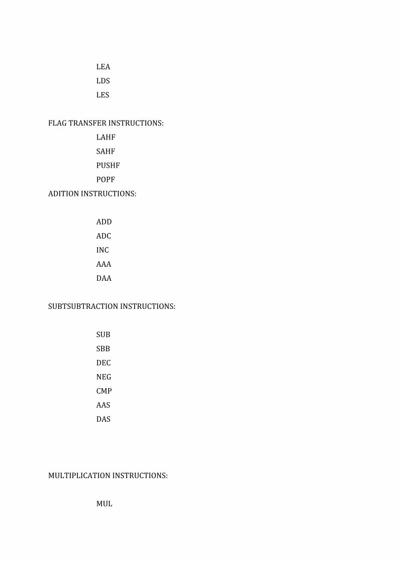
LEA
LDS
LES
FLAG TRANSFER INSTRUCTIONS:
LAHF
SAHF
PUSHF
POPF
ADITION INSTRUCTIONS:
ADD
ADC
INC
AAA
DAA
SUBTSUBTRACTION INSTRUCTIONS:
SUB
SBB
DEC
NEG
CMP
AAS
DAS
MULTIPLICATION INSTRUCTIONS:
MUL
IMUL
AAM
DIVISION INSTRUCTIONS:
DIV
IDIV
AAD
CBW
CWD
BIT MANIPULATION INSTRUCTIONS
LOGICAL INSTRUCTIONS:
NOT
AND
OR
XOR
TEST
SHIFT INSTRUCTIONS:
SHL / SAL
SHR
SAR
PROGRAM EXECUTION TRANSFER INSTRUCTIONS
UNCONDITIONAL TRANSFER INSTRUCTIONS:
CALL
RET
JMP
CONDITIONAL TRANSFER INSTRUCTIONS:
JA / JNBE
JAE / JNB
JB / JNAE
JBE / JNA

JC
JE / JZ
JG / JNLE
JGE / JNL
JL / JNGE
JLE / JNG
R JNC
JNE / JNZ
JNO
JNP / JPO
JNS
JO
JP / JPE
JS
ITERATION CONTROL INSTRUCTIONS:
LOOP
LOOPE / LOOPZ
LOOPNE / LOOPNZ
JCXZ
INTERRUPT INSTRUCTIONS:
INT
INTO
IRET
PROCESS CONTROL INSTRUCTIONS
FLAG SET / CLEAR INSTRUCTIONS:
STC
CLC
CMC
STD
CLD
STI
CLI
EXTERNAL HARDWARE SYNCHRONIZATION INSTRUCTIONS:
HLT
WAIT
ESC
LOCK
NOP
Instruction Description
AAA Instruction - ASCII Adjust after Addition
AAD Instruction - ASCII adjust before Division
AAM Instruction - ASCII adjust after Multiplication
AAS Instruction - ASCII Adjust for Subtraction
ADC Instruction - Add with carry.
ADD Instruction - ADD destination, source
AND Instruction - AND corresponding bits of two operands
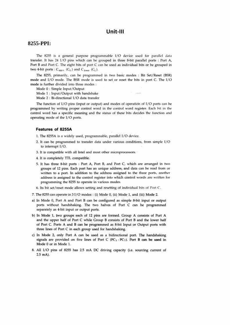
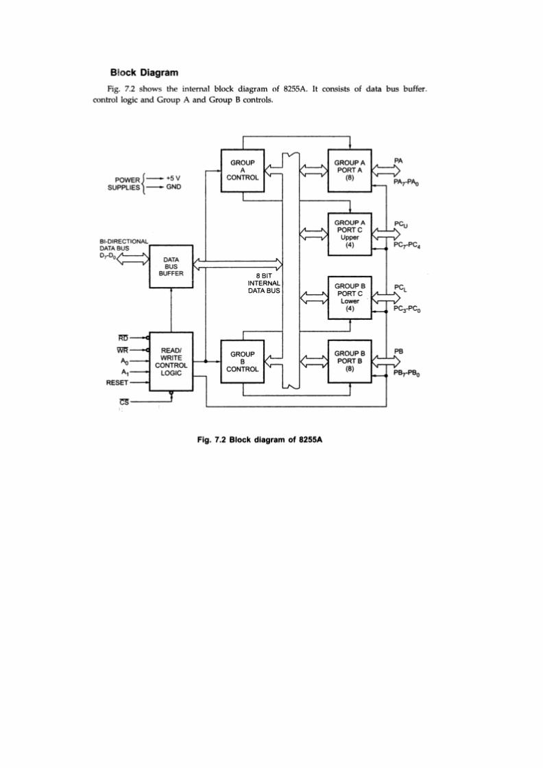
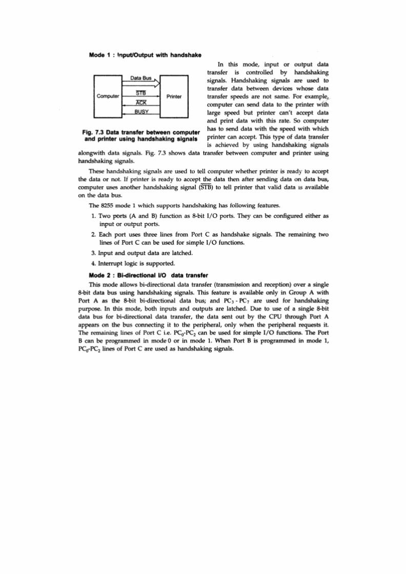
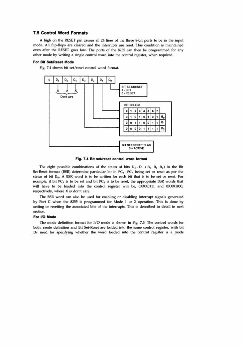
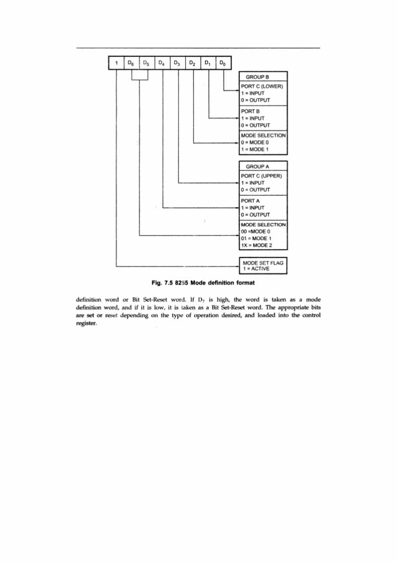
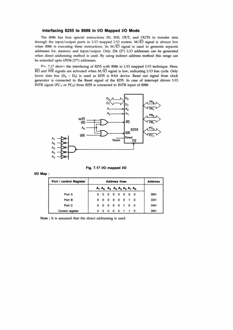
Unit-III
8255-PPI:

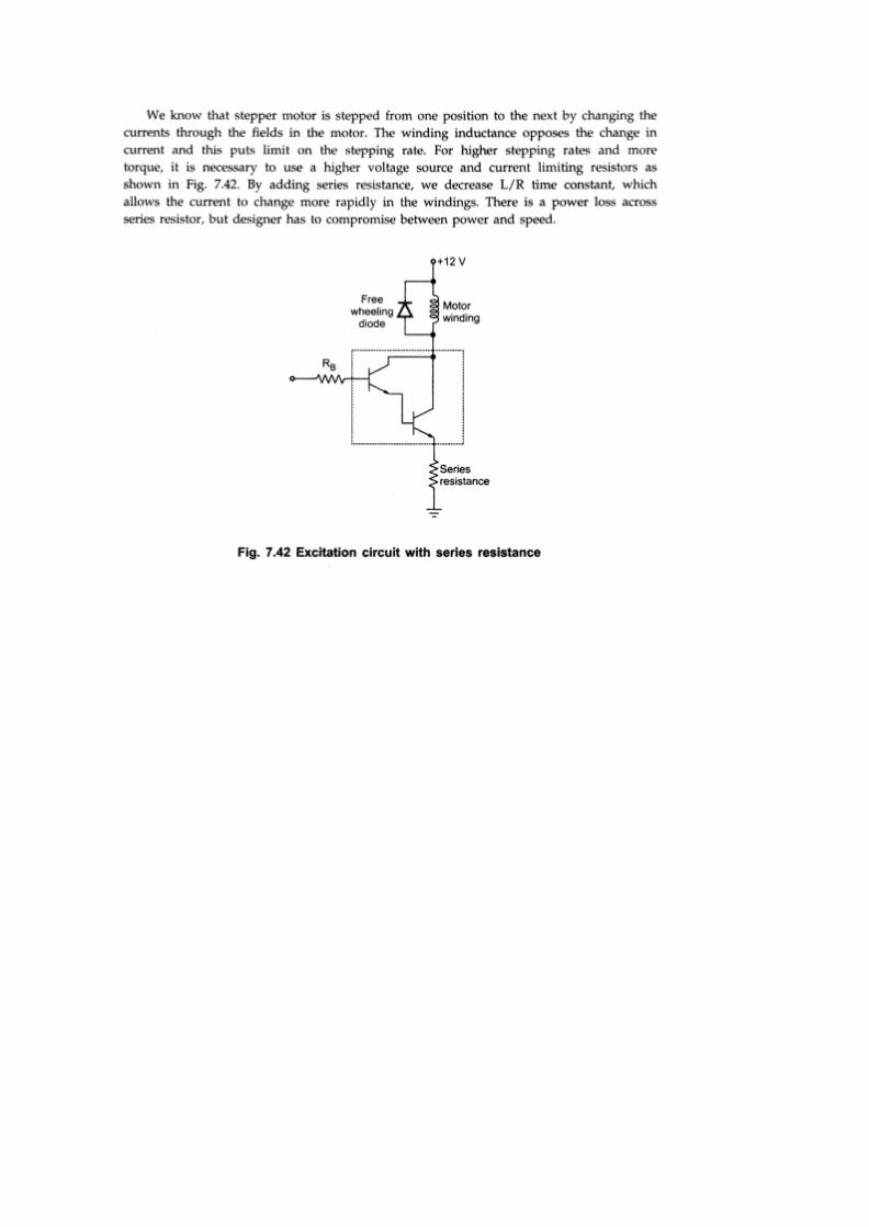
MEMORY INTERFACING:
•Control connections: A ROM usually has only one control input, while a RAM often has
one or two control inputs.
•The control input most often found on the ROM is the output enable ( OE ) or gate ( G
), this allows data to flow out of the output data pins of the ROM.
•If OE and the selected input are both active, then the output is enable, if OE is inactive,
the output is disabled at its high-impedance state.
•The OE connection enables and disables a set of three-state buffer located within the
memory device and must be active to read data.
•A RAM memory device has either one or two control inputs. If there is one control
input it is often called R/ W .
•This pin selects a read operation or a write operation only if the device is selected by
the selection input ( CS ). If the RAM has two control inputs, they are usually labeled WE
or W and OE or G .
•( WE ) write enable must be active to perform a memory write operation and OE must
be active to perform a memory read operation.
•When these two controls WE and OE are present, they must never be active at the
same time.
•The ROM read only memory permanently stores programs and data and data was
always present, even when power is disconnected.
•It is also called as nonvolatile memory.
•EPROM ( erasable programmable read only memory ) is also erasable if exposed to
high intensity ultraviolet light for about 20 minutes or less, depending upon the type of
EPROM.
•We have PROM (programmable read only memory )
•RMM ( read mostly memory ) is also called the flash memory.
•The flash memory is also called as an EEPROM (electrically erasable
programmable ROM), EAROM ( electrically alterable ROM ), or a NOVROM ( nonvolatile
ROM ).
•These memory devices are electrically erasable in the system, but require more time to
erase than a normal RAM.
•EPROM contains the series of 27XXX contains the following part numbers :
2704( 512 * 8 ), 2708(1K * 8 ), 2716( 2K * 8 ), 2732( 4K * 8 ), 2764( 8K * 8 ), 27128( 16K
* 8) etc..
•Each of these parts contains address pins, eight data connections, one or more chip
selection inputs ( CE ) and an output enable pin ( OE ).
•This device contains 11 address inputs and 8 data outputs.
•If both the pin connection CE and OE are at logic 0, data will appear on the output
connection . If both the pins are not at logic 0, the data output connections remains at
their high impedance or off state.
•To read data from the EPROM Vpp pin must be placed at a logic 1.
Static RAM Interfacing
The semiconductor RAM is broadly two types – Static RAM and Dynamic RAM.
•The semiconductor memories are organized as two dimensional arrays of memory
locations.
•For example 4K * 8 or 4K byte memory contains 4096 locations, where each locations
contains 8-bit data and only one of the 4096 locations can be selected at a time. Once a
location is selected all the bits in it are accessible using a group of conductors called
Data bus.
•For addressing the 4K bytes of memory, 12 address lines are required.
•In general to address a memory location out of N memory locations, we will require at
least n bits of address, i.e. n address lines where n = Log2 N.
•Thus if the microprocessor has n address lines, then it is able to address at the most N
locations of memory, where 2n=N. If out of N locations only P memory locations are to
be interfaced, then the least significant p address lines out of the available n lines can be
directly connected from the microprocessor to the memory chip while the remaining (n-
p) higher order address lines may be used for address decoding as inputs to the chip
selection logic.
•The memory address depends upon the hardware circuit used for decoding the chip
select ( CS ). The output of the decoding circuit is connected with the CS pin of the
memory chip.
•The general procedure of static memory interfacing with 8086 is briefly described as
follows:
1.Arrange the available memory chip so as to obtain 16- bit data bus width. The upper 8-
bit bank is called as odd address memory bank and the lower 8-bit bank is called as

even address memory bank.
2.Connect available memory address lines of memory chip with those of the
microprocessor and also connect the memory RD and WR inputs to the corresponding
processor control signals. Connect the 16-bit data bus of the memory bank with that of
the microprocessor 8086.
3.The remaining address lines of the microprocessor, BHE and A0 are used for decoding
the required chip select signals for the odd and even memory banks. The CS of memory
is derived from the o/p of the decoding circuit.
•As a good and efficient interfacing practice, the address map of the system should be
continuous as far as possible, i.e. there should not be no windows in the mapand no fold
back space should be allowed. A memory location should have a single address
corresponding to it, i.e. absolute decoding should be preferred and minimum hardware
should be used for decoding large capacity memory is required in a microcomputer
system, the memory subsystem is generally designed using dynamic RAM because there
are various advantages of dynamic RAM.
• E.g. higher packing density, lower cost and less power consumption. A typical static
RAM cell may require six transistors while the dynamic RAM cell requires only a
transistors along with a capacitor. Hence it is possible to obtain higher packaging
density and hence low cost units are available.
•The basic dynamic RAM cell uses a capacitor to store the charge as a representation of
data. This capacitor is manufactured as a diode that is reverse- biased so that the
storage capacitance comes into the picture.
•This storage capacitance is utilized for storing the charge representation of data but
the reverse-biased diode has leakage current that tends to discharge the capacitor
giving rise to the possibility of data loss. To avoid this possible data loss, the data stored
in a dynamic RAM cell must be refreshed after a fixed time interval regularly. The
process of refreshing the data in RAM is called as
Refresh cycle.
•The refresh activity is similar to reading the data from each and every cell of memory,
independent of the requirement of microprocessor. During this refresh period all other
operations related to the memory subsystem are suspended. Hence the refresh activity
causes loss of time, resulting in reduce system performance.
•However keeping in view the advantages of dynamic RAM, like low power
consumption, high packaging density and low cost, most of the advanced computing
system are designed using dynamic RAM, at the cost of operating
speed.
• A dedicated hardware chip called as dynamic RAM controller is the most important
part of the interfacing circuit.
•The Refresh cycle is different from the memory read cycle in the following aspects.
1.The memory address is not provided by the CPU address bus, rather it is generated by
a refresh mechanism counter called as refresh counter.
2.Unlike memory read cycle, more than one memory chip may be enabled at a time so
as to reduce the number of total memory refresh cycles.
3.The data enable control of the selected memory chip is deactivated, and data is not
allowed to appear on the system data bus during refresh, as more than one memory
units are refreshed simultaneously. This is to avoid the data from the different chips to
appear on the bus simultaneously.
4.Memory read is either a processor initiated or an external bus master initiated and
carried out by the refresh mechanism. Dynamic RAM is available in units of several
kilobits to megabits of memory.
This memory is arranged internally in a two dimensional matrix array so that it will
have n rows and m columns. The row address n and column address m are important
for the refreshing operation.
• For example, a typical 4K bit dynamic RAM chip has an internally arranged bit array of
dimension 64 * 64 , i.e. 64 rows and 64 columns. The row address and column address
will require 6 bits each. These 6 bits for each row address and column address will be
generated by the refresh counter, during the refresh cycles.
•A complete row of 64 cells is refreshed at a time to minimizes the refreshing time.
Thus the refresh counter needs to generate only row addresses. The row address are
multiplexed, over lower order address lines.
•The refresh signals act to control the multiplexer, i.e. when refresh cycle is in process
the refresh counter puts the row address over the address bus for refreshing.
Otherwise, the address bus of the processor is connected to the address bus of DRAM,
during normal processor initiated activities.
• A timer, called refresh timer, derives a pulse for refreshing action after each refresh
interval.
•Refresh interval can be qualitatively defined as the time for which a dynamic RAM cell
can hold data charge level practically constant, i.e. no data loss takes place.
• Suppose the typical dynamic RAM chip has 64 rows, then each row should be
refreshed after each refresh interval or in other words, all the 64 rows are to refreshed
in a single refresh interval.
•This refresh interval depends upon the manufacturing technology of the dynamic RAM
cell. It may range anywhere from 1ms to 3ms.
• Let us consider 2ms as a typical refresh time interval. Hence, the frequency of the
refresh pulses will be calculated as follows:
•Refresh Time ( per row ) tr = (2 * 10 -3) / 64.
•Refresh Frequency fr = 64 / ( 2 * 10 -3) = 32 * 103 Hz.
•The following block diagram explains the refreshing logic and 8086 interfacing with
dynamic RAM.
•Each chip is of 16K * 1-bit dynamic RAM cell array. The system contains two 16K byte
dynamic RAM units. All the address and data lines are assumed to be available from an
8086 microprocessor system.
•The OE pin controls output data buffer of the memory chips. The CE pins are active
high chip selects of memory chips. The refresh cycle starts, if the refresh output of the
refresh timer goes high, OE and CE also tend to go high.
•The high CE enables the memory chip for refreshing, while high OE prevents the data
from appearing on the data bus, as discussed in memory refresh cycle. The 16K * 1-bit
dynamic RAM has an internal array of 128*128 cells, requiring 7 bits for row address.
The lower order seven lines A0-A6 are multiplexed with the refresh counter output A10-
A16.
•If the RAM has two control inputs, they are usually labeled WE or W and OE or G .
•( WE ) write enable must be active to perform a memory write operation and OE must
be active to perform a memory read operation.
•When these two controls WE and OE are present, they must never be active at the
same time
•The ROM read only memory permanently stores programs and data and data was
always present, even when power is disconnected.
•It is also called as nonvolatile memory.
•EPROM ( erasable programmable read only memory ) is also erasable if exposed to
high intensity ultraviolet light for about 20 minutes or less, depending upon the type of
EPROM.
•We have PROM (programmable read only memory )
•RMM ( read mostly memory ) is also called the flash memory.
•The flash memory is also called as an EEPROM (electrically erasable programmable
ROM), EAROM ( electrically alterable ROM ), or a NOVROM ( nonvolatile ROM ).
•These memory devices are electrically erasable in the system, but require more time to
erase than a normal RAM.
•EPROM contains the series of 27XXX contains the following part numbers :
2704( 512 * 8 ), 2708(1K * 8 ), 2716( 2K * 8 ), 2732( 4K * 8 ), 2764( 8K * 8 ), 27128( 16K
* 8) etc..
•Each of these parts contains address pins, eight data connections, one or more chip
selection inputs ( CE ) and an output enable pin ( OE ).
•This device contains 11 address inputs and 8 data outputs.
•If both the pin connection CE and OE are at logic 0, data will appear on the output
connection . If both the pins are not at logic 0, the data output connections remains at
their high impedance or off state.
•To read data from the EPROM Vpp pin must be placed at a logic 1.
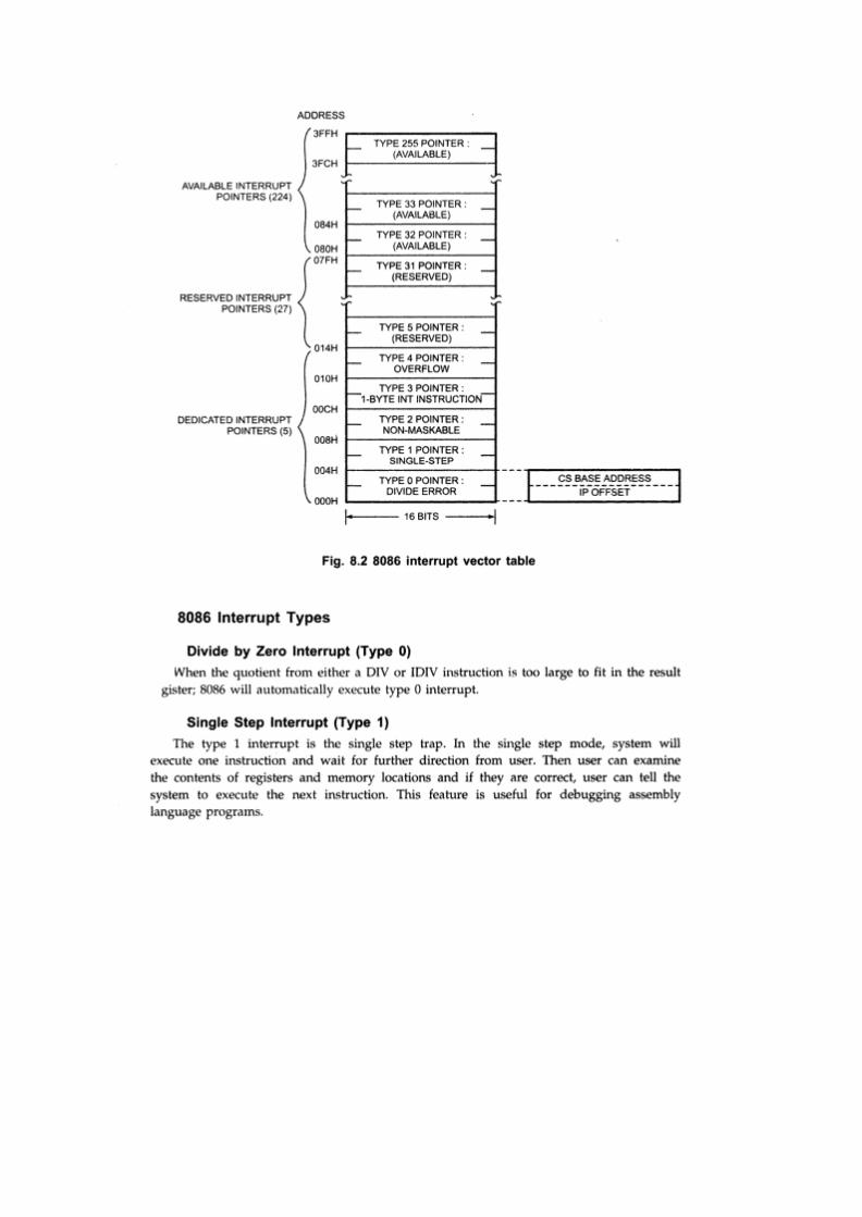
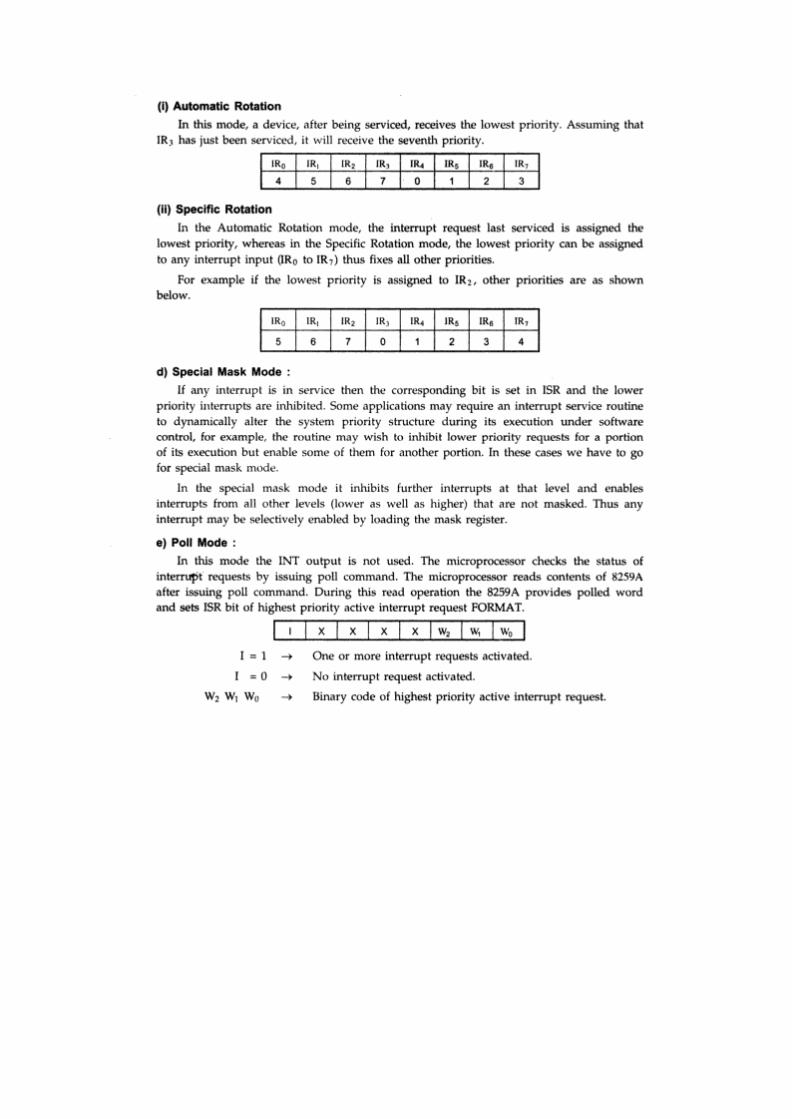
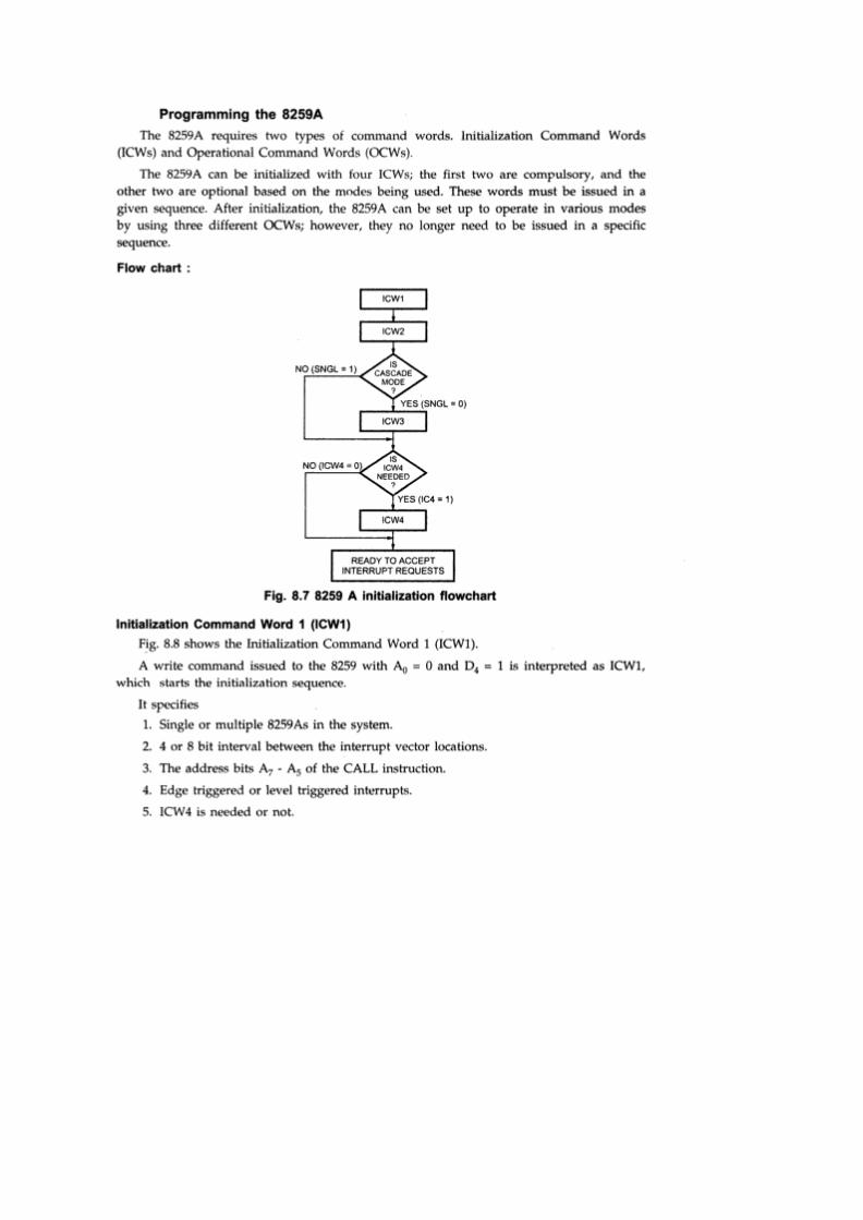
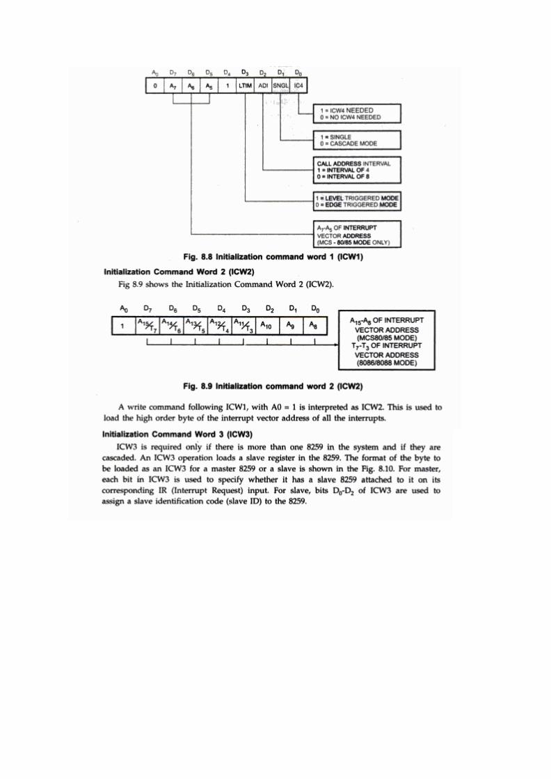
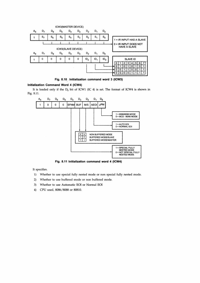
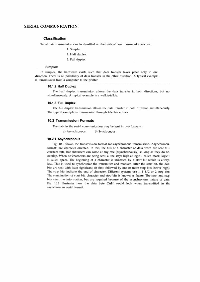
SERIAL COMMUNICATION:
Universal Synchronous Asynchronous Receiver Transmitter (USART)
The 8251 is a USART (Universal Synchronous Asynchronous Receiver Transmitter) for
serial data communication. As a peripheral device of a microcomputer system, the 8251
receives parallel data from the CPU and transmits serial data after conversion. This device
also receives serial data from the outside and transmits parallel data to the CPU after
conversion.
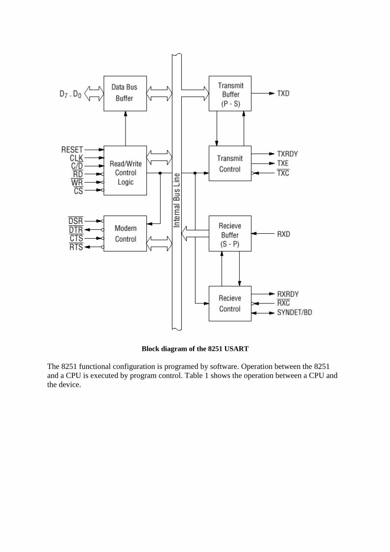
Block diagram of the 8251 USART
The 8251 functional configuration is programed by software. Operation between the 8251
and a CPU is executed by program control. Table 1 shows the operation between a CPU and
the device.
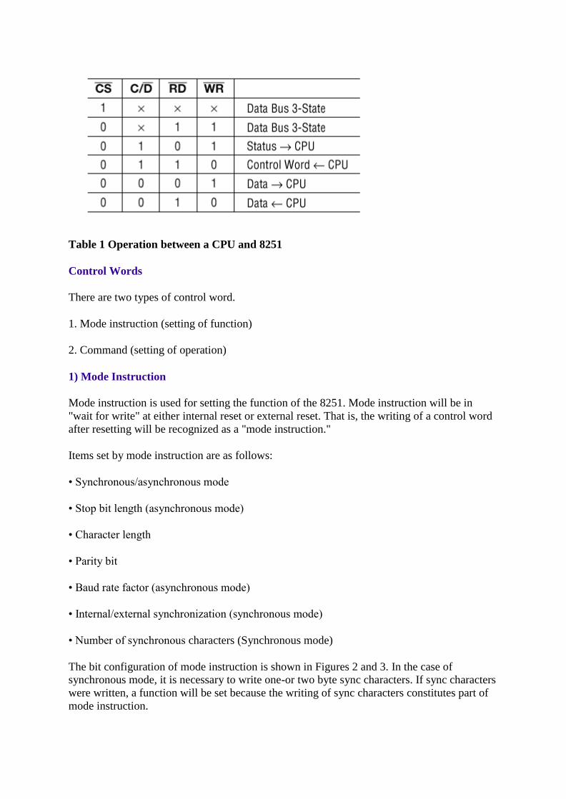
Table 1 Operation between a CPU and 8251
Control Words
There are two types of control word.
1. Mode instruction (setting of function)
2. Command (setting of operation)
1) Mode Instruction
Mode instruction is used for setting the function of the 8251. Mode instruction will be in
"wait for write" at either internal reset or external reset. That is, the writing of a control word
after resetting will be recognized as a "mode instruction."
Items set by mode instruction are as follows:
• Synchronous/asynchronous mode
• Stop bit length (asynchronous mode)
• Character length
• Parity bit
• Baud rate factor (asynchronous mode)
• Internal/external synchronization (synchronous mode)
• Number of synchronous characters (Synchronous mode)
The bit configuration of mode instruction is shown in Figures 2 and 3. In the case of
synchronous mode, it is necessary to write one-or two byte sync characters. If sync characters
were written, a function will be set because the writing of sync characters constitutes part of
mode instruction.
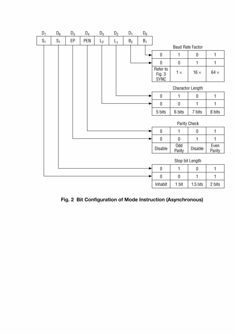
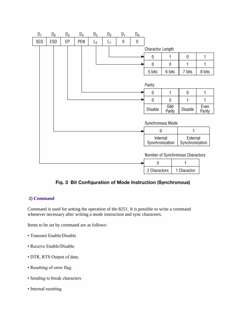
2) Command
Command is used for setting the operation of the 8251. It is possible to write a command
whenever necessary after writing a mode instruction and sync characters.
Items to be set by command are as follows:
• Transmit Enable/Disable
• Receive Enable/Disable
• DTR, RTS Output of data.
• Resetting of error flag.
• Sending to break characters
• Internal resetting
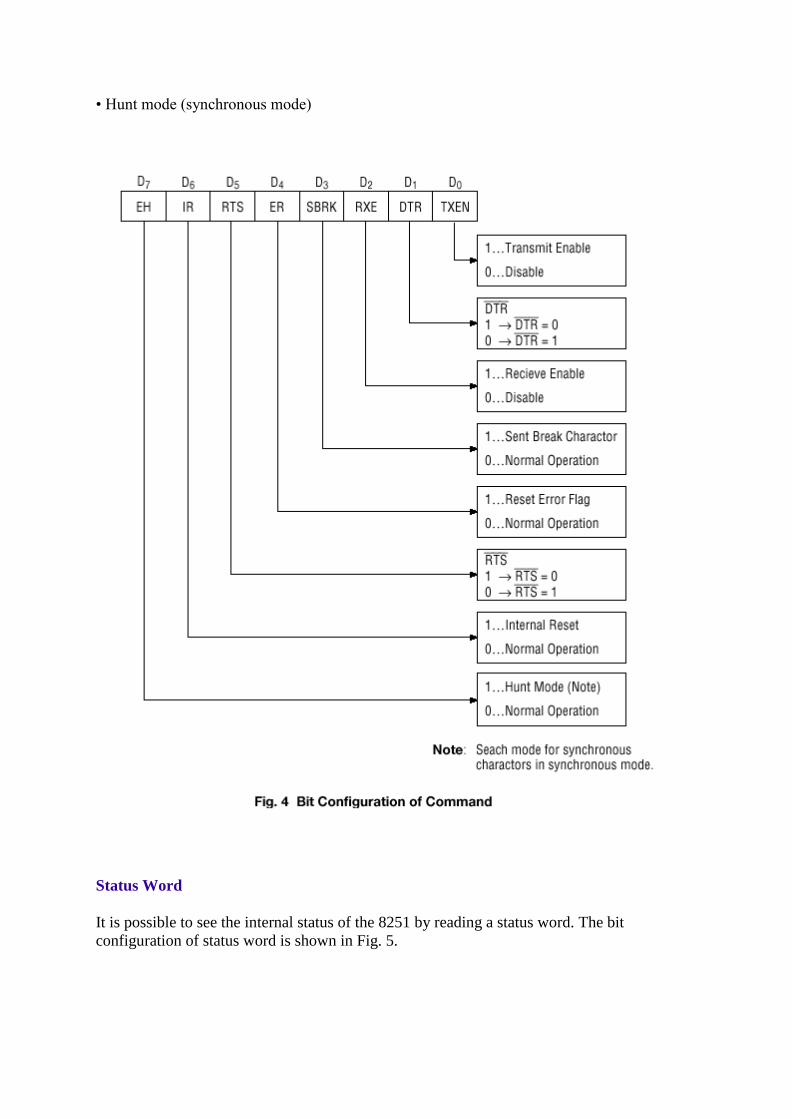
• Hunt mode (synchronous mode)
Status Word
It is possible to see the internal status of the 8251 by reading a status word. The bit
configuration of status word is shown in Fig. 5.
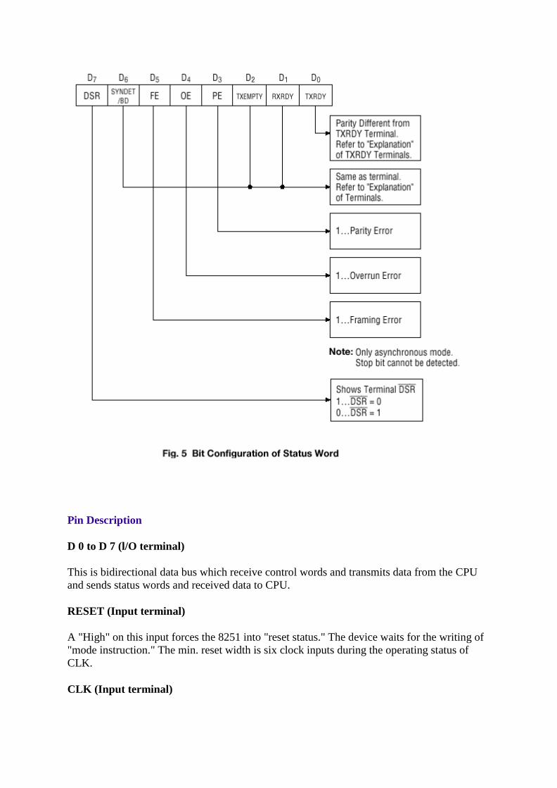
Pin Description
D 0 to D 7 (l/O terminal)
This is bidirectional data bus which receive control words and transmits data from the CPU
and sends status words and received data to CPU.
RESET (Input terminal)
A "High" on this input forces the 8251 into "reset status." The device waits for the writing of
"mode instruction." The min. reset width is six clock inputs during the operating status of
CLK.
CLK (Input terminal)
CLK signal is used to generate internal device timing. CLK signal is independent of RXC or
TXC. However, the frequency of CLK must be greater than 30 times the RXC and TXC at
Synchronous mode and Asynchronous "x1" mode, and must be greater than 5 times at
Asynchronous "x16" and "x64" mode.
WR (Input terminal)
This is the "active low" input terminal which receives a signal for writing transmit data and
control words from the CPU into the 8251.
RD (Input terminal)
This is the "active low" input terminal which receives a signal for reading receive data and
status words from the 8251.
C/D (Input terminal)
This is an input terminal which receives a signal for selecting data or command words and
status words when the 8251 is accessed by the CPU. If C/D = low, data will be accessed. If
C/D = high, command word or status word will be accessed.
CS (Input terminal)
This is the "active low" input terminal which selects the 8251 at low level when the CPU
accesses. Note: The device won‘t be in "standby status"; only setting CS = High.
TXD (output terminal)
This is an output terminal for transmitting data from which serial-converted data is sent out.
The device is in "mark status" (high level) after resetting or during a status when transmit is
disabled. It is also possible to set the device in "break status" (low level) by a command.
TXRDY (output terminal)
This is an output terminal which indicates that the 8251is ready to accept a transmitted data
character. But the terminal is always at low level if CTS = high or the device was set in "TX
disable status" by a command. Note: TXRDY status word indicates that transmit data
character is receivable, regardless of CTS or command. If the CPU writes a data character,
TXRDY will be reset by the leading edge or WR signal.
TXEMPTY (Output terminal)
This is an output terminal which indicates that the 8251 has transmitted all the characters and
had no data character. In "synchronous mode," the terminal is at high level, if transmit data
characters are no longer remaining and sync characters are automatically transmitted. If the
CPU writes a data character, TXEMPTY will be reset by the leading edge of WR signal. Note
: As the transmitter is disabled by setting CTS "High" or command, data written before
disable will be sent out. Then TXD and TXEMPTY will be "High". Even if a data is written
after disable, that data is not sent out and TXE will be "High".After the transmitter is enabled,
it sent out. (Refer to Timing Chart of Transmitter Control and Flag Timing)
TXC (Input terminal)
This is a clock input signal which determines the transfer speed of transmitted data. In
"synchronous mode," the baud rate will be the same as the frequency of TXC. In
"asynchronous mode", it is possible to select the baud rate factor by mode instruction. It can
be 1, 1/16 or 1/64 the TXC. The falling edge of TXC sifts the serial data out of the 8251.
RXD (input terminal)
This is a terminal which receives serial data.
RXRDY (Output terminal)
This is a terminal which indicates that the 8251 contains a character that is ready to READ. If
the CPU reads a data character, RXRDY will be reset by the leading edge of RD signal.
Unless the CPU reads a data character before the next one is received completely, the
preceding data will be lost. In such a case, an overrun error flag status word will be set.
RXC (Input terminal)
This is a clock input signal which determines the transfer speed of received data. In
"synchronous mode," the baud rate is the same as the frequency of RXC. In "asynchronous
mode," it is possible to select the baud rate factor by mode instruction. It can be 1, 1/16, 1/64
the RXC.
SYNDET/BD (Input or output terminal)
This is a terminal whose function changes according to mode. In "internal synchronous
mode." this terminal is at high level, if sync characters are received and synchronized. If a
status word is read, the terminal will be reset. In "external synchronous mode, "this is an
input terminal. A "High" on this input forces the 8251 to start receiving data characters.
In "asynchronous mode," this is an output terminal which generates "high level"output upon
the detection of a "break" character if receiver data contains a "low-level" space between the
stop bits of two continuous characters. The terminal will be reset, if RXD is at high level.
After Reset is active, the terminal will be output at low level.
DSR (Input terminal)
This is an input port for MODEM interface. The input status of the terminal can be
recognized by the CPU reading status words.
DTR (Output terminal)
This is an output port for MODEM interface. It is possible to set the status of DTR by a
command.
CTS (Input terminal)
This is an input terminal for MODEM interface which is used for controlling a transmit
circuit. The terminal controls data transmission if the device is set in "TX Enable" status by a
command. Data is transmitable if the terminal is at low level.
RTS (Output terminal)
This is an output port for MODEM interface. It is possible to set the status RTS by a
command.
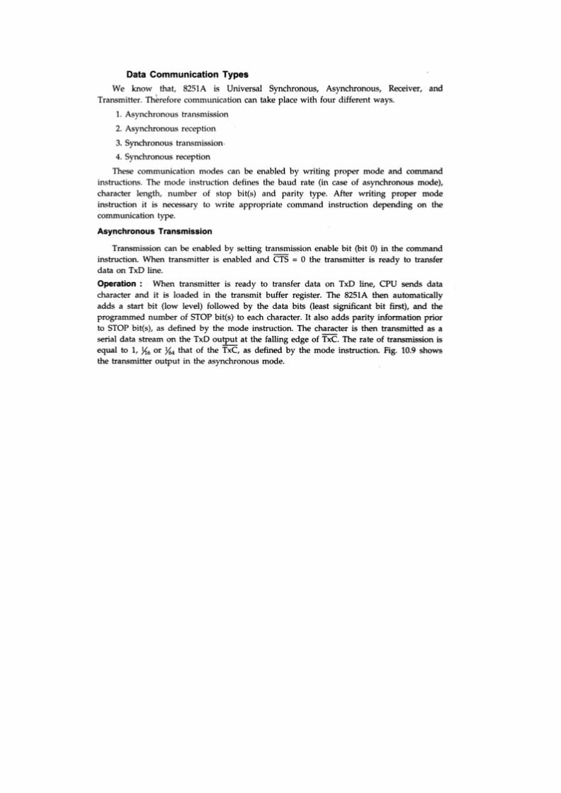
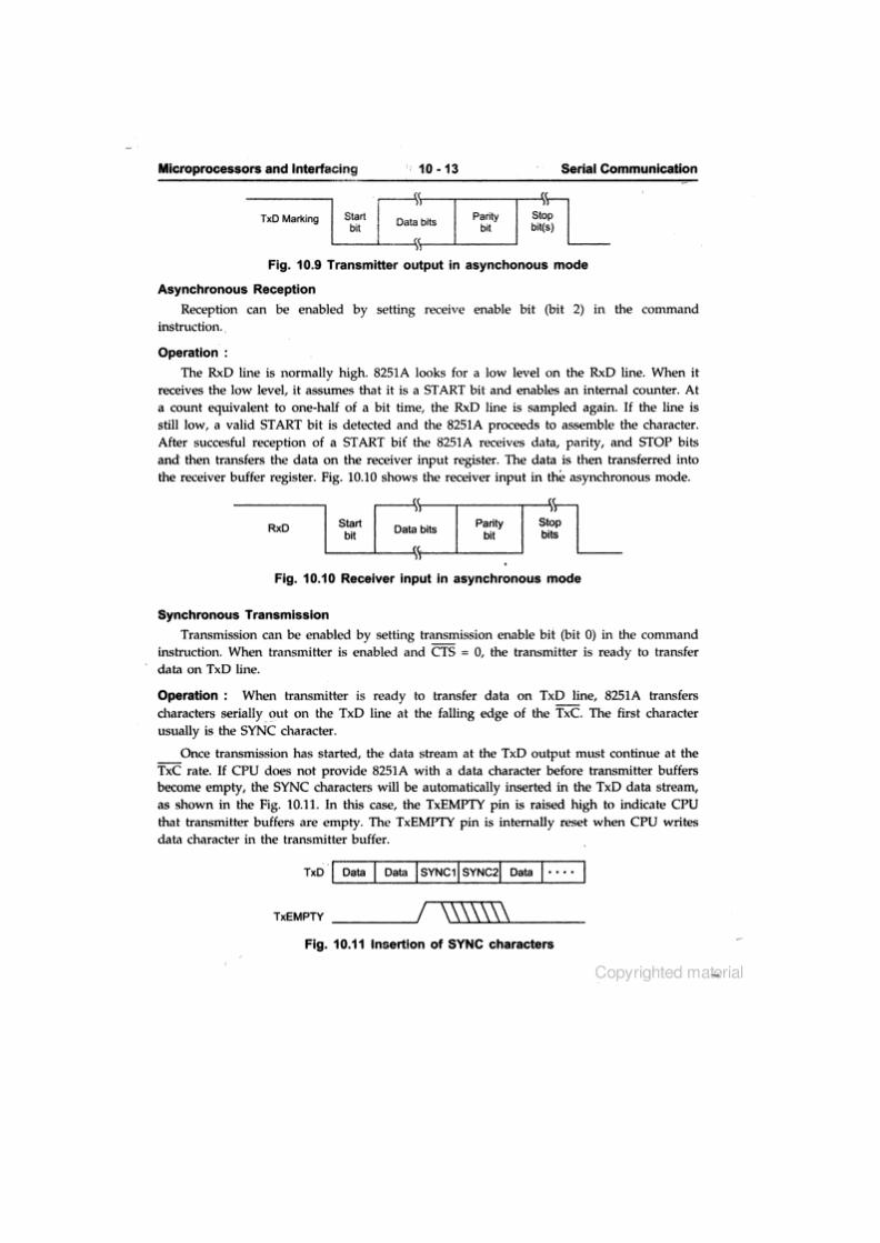
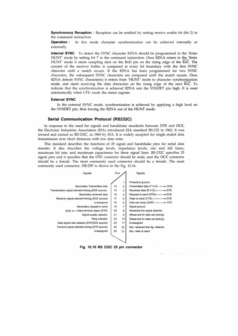
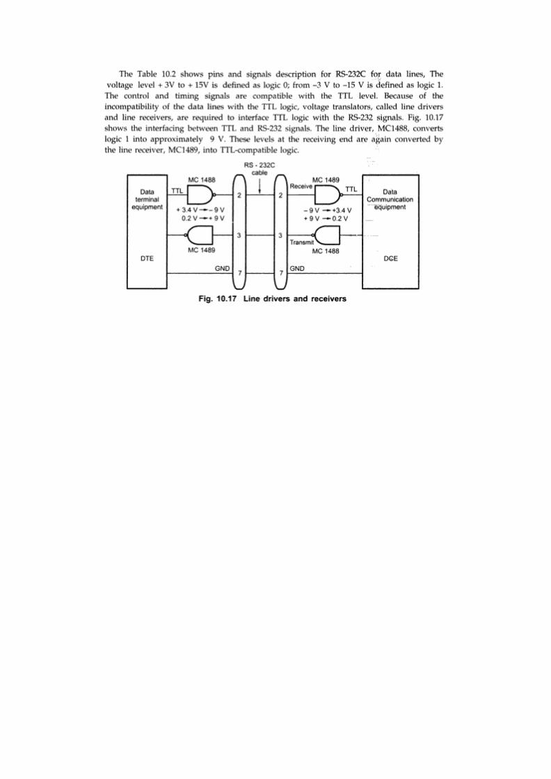
UNIT-IV
8051 MICROCONTROLLER:
The Intel 8051 microcontroller is one of the most popular general purpose
microcontrollers in use today. The success of the Intel 8051 spawned a number of clones
which are collectively referred to as the MCS-51 family of microcontrollers, which includes
chips from vendors such as Atmel, Philips, Infineon, and Texas Instruments
The Intel 8051 is an 8-bit microcontroller which means that most available operations are
limited to 8 bits. There are 3 basic "sizes" of the 8051: Short, Standard, and Extended. The
Short and Standard chips are often available in DIP (dual in-line package) form, but the
Extended 8051 models often have a different form factor, and are not "drop-in compatible".
All these things are called 8051 because they can all be programmed using 8051 assembly
language, and they all share certain features (although the different models all have their own
special features).
Some of the features that have made the 8051 popular are:
64 KB on chip program memory.
128 bytes on chip data memory(RAM).
4 reg banks.
128 user defined software flags.
8-bit data bus
16-bit address bus
32 general purpose registers each of 8 bits
16 bit timers (usually 2, but may have more, or less).
3 internal and 2 external interrupts.
Bit as well as byte addressable RAM area of 16 bytes.
Four 8-bit ports, (short models have two 8-bit ports).
16-bit program counter and data pointer.
1 Microsecond instruction cycle with 12 MHz Crystal.
8051 models may also have a number of special, model-specific features, such as UARTs,
ADC, OpAmps, etc...
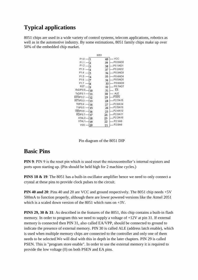
Typical applications
8051 chips are used in a wide variety of control systems, telecom applications, robotics as
well as in the automotive industry. By some estimations, 8051 family chips make up over
50% of the embedded chip market.
Pin diagram of the 8051 DIP
Basic Pins
PIN 9: PIN 9 is the reset pin which is used reset the microcontroller‘s internal registers and
ports upon starting up. (Pin should be held high for 2 machine cycles.)
PINS 18 & 19: The 8051 has a built-in oscillator amplifier hence we need to only connect a
crystal at these pins to provide clock pulses to the circuit.
PIN 40 and 20: Pins 40 and 20 are VCC and ground respectively. The 8051 chip needs +5V
500mA to function properly, although there are lower powered versions like the Atmel 2051
which is a scaled down version of the 8051 which runs on +3V.
PINS 29, 30 & 31: As described in the features of the 8051, this chip contains a built-in flash
memory. In order to program this we need to supply a voltage of +12V at pin 31. If external
memory is connected then PIN 31, also called EA/VPP, should be connected to ground to
indicate the presence of external memory. PIN 30 is called ALE (address latch enable), which
is used when multiple memory chips are connected to the controller and only one of them
needs to be selected.We will deal with this in depth in the later chapters. PIN 29 is called
PSEN. This is "program store enable". In order to use the external memory it is required to
provide the low voltage (0) on both PSEN and EA pins.
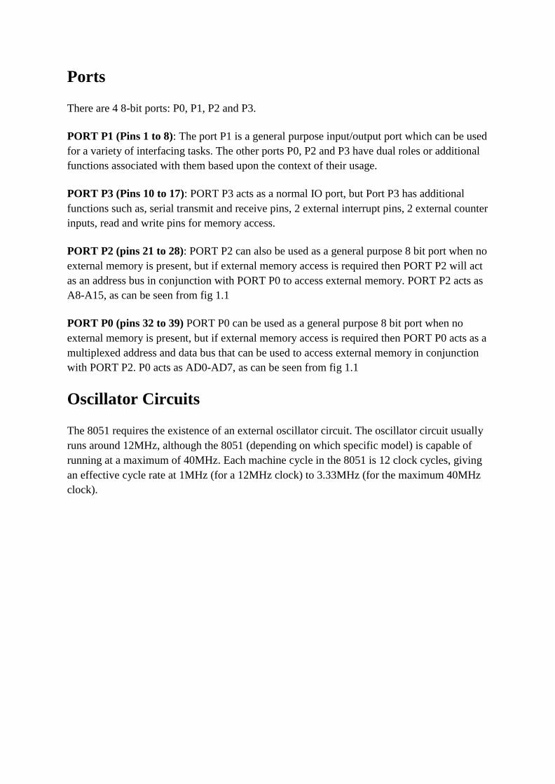
Ports
There are 4 8-bit ports: P0, P1, P2 and P3.
PORT P1 (Pins 1 to 8): The port P1 is a general purpose input/output port which can be used
for a variety of interfacing tasks. The other ports P0, P2 and P3 have dual roles or additional
functions associated with them based upon the context of their usage.
PORT P3 (Pins 10 to 17): PORT P3 acts as a normal IO port, but Port P3 has additional
functions such as, serial transmit and receive pins, 2 external interrupt pins, 2 external counter
inputs, read and write pins for memory access.
PORT P2 (pins 21 to 28): PORT P2 can also be used as a general purpose 8 bit port when no
external memory is present, but if external memory access is required then PORT P2 will act
as an address bus in conjunction with PORT P0 to access external memory. PORT P2 acts as
A8-A15, as can be seen from fig 1.1
PORT P0 (pins 32 to 39) PORT P0 can be used as a general purpose 8 bit port when no
external memory is present, but if external memory access is required then PORT P0 acts as a
multiplexed address and data bus that can be used to access external memory in conjunction
with PORT P2. P0 acts as AD0-AD7, as can be seen from fig 1.1
Oscillator Circuits
The 8051 requires the existence of an external oscillator circuit. The oscillator circuit usually
runs around 12MHz, although the 8051 (depending on which specific model) is capable of
running at a maximum of 40MHz. Each machine cycle in the 8051 is 12 clock cycles, giving
an effective cycle rate at 1MHz (for a 12MHz clock) to 3.33MHz (for the maximum 40MHz
clock).
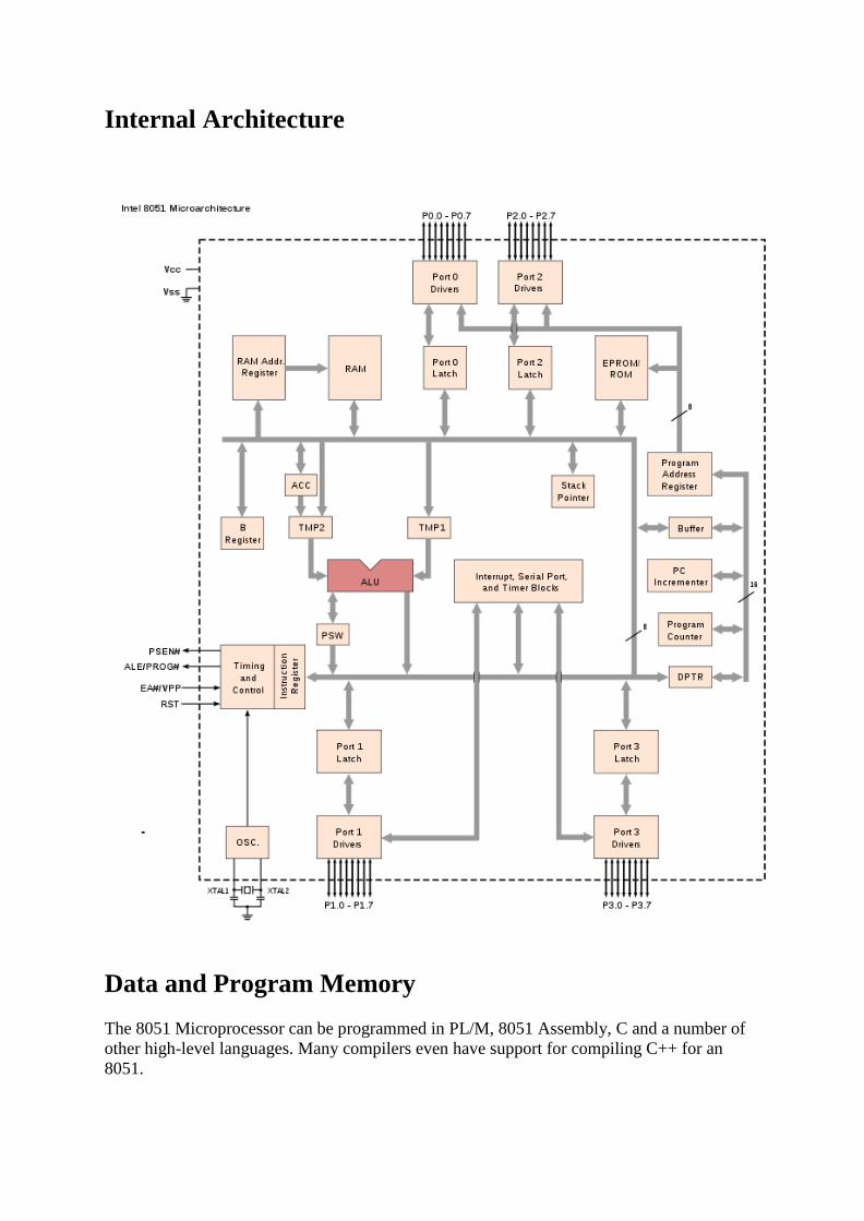
Internal Architecture
Data and Program Memory
The 8051 Microprocessor can be programmed in PL/M, 8051 Assembly, C and a number of
other high-level languages. Many compilers even have support for compiling C++ for an
8051.

Program memory in the 8051 is read-only, while the data memory is considered to be
read/write accessible. When stored on EEPROM or Flash, the program memory can be
rewritten when the microcontroller is in the special programmer circuit.
Program Start Address
The 8051 starts executing program instructions from address 0000 in the program memory.
Direct Memory
The 8051 has 256 bytes of internal addressable RAM, although only the first 128 bytes are
available for general use by the programmer. The first 128 bytes of RAM (from 0x00 to
0x7F) are called the Direct Memory, and can be used to store data.
Special Function Register
The Special Function Register (SFR) is the upper area of addressable memory, from address
0x80 to 0xFF. A, B, PSW, DPTR are called SFR.This area of memory cannot be used for data
or program storage, but is instead a series of memory-mapped ports and registers. All port
input and output can therefore be performed by memory mov operations on specified
addresses in the SFR. Also, different status registers are mapped into the SFR, for use in
checking the status of the 8051, and changing some operational parameters of the 8051.
General Purpose Registers
The 8051 has 4 selectable banks of 8 addressable 8-bit registers, R0 to R7. This means that
there are essentially 32 available general purpose registers, although only 8 (one bank) can be
directly accessed at a time. To access the other banks, we need to change the current bank
number in the flag status register.
A and B Registers
The A register is located in the SFR memory location 0xE0. The A register works in a similar
fashion to the AX register of x86 processors. The A register is called the accumulator, and
by default it receives the result of all arithmetic operations. The B register is used in a similar
manner, except that it can receive the extended answers from the multiply and divide
operations. When not being used for multiplication and Division, the B register is available as
an extra general-purpose register.
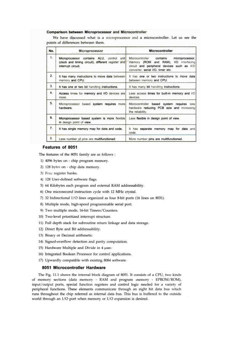

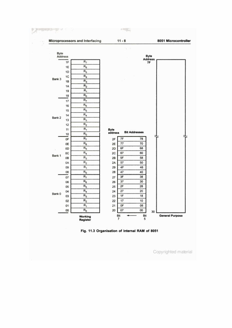
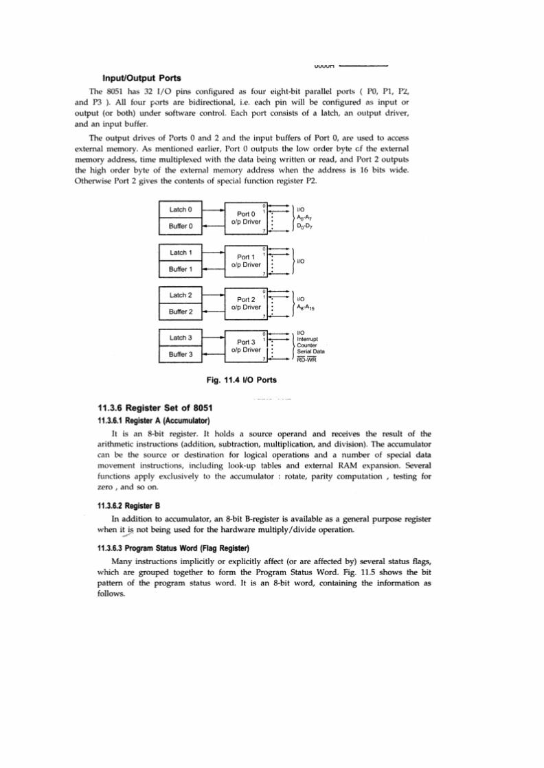
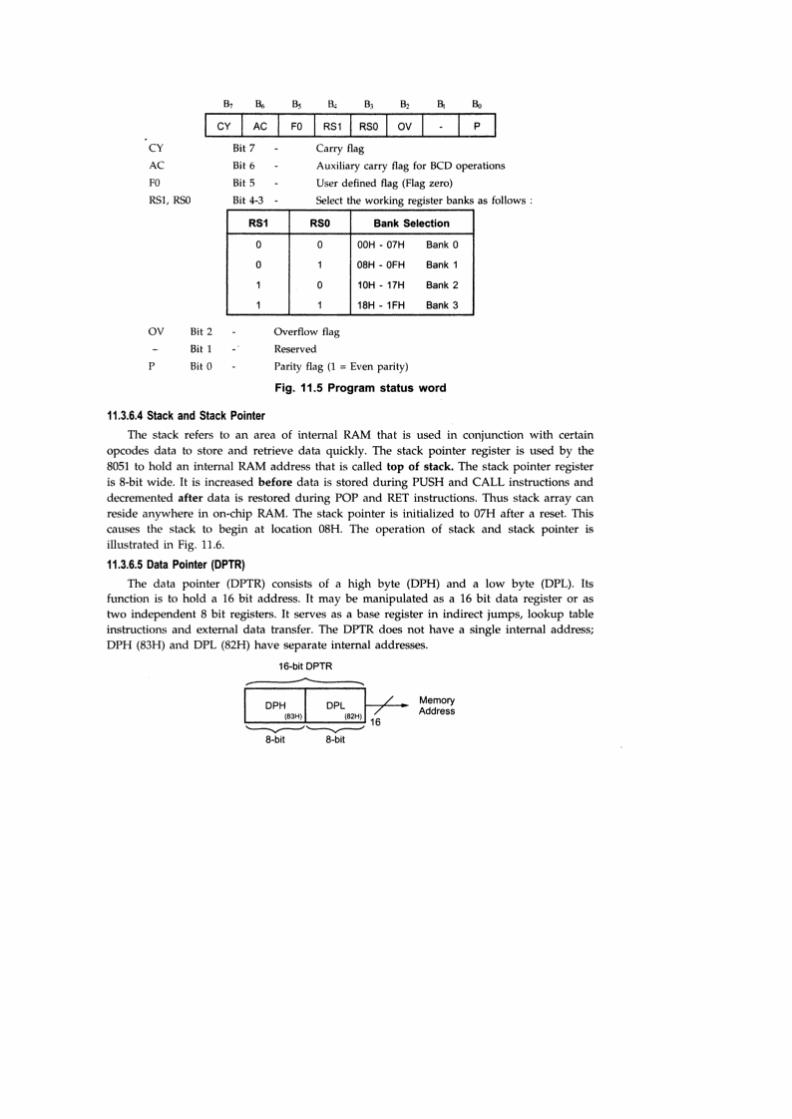
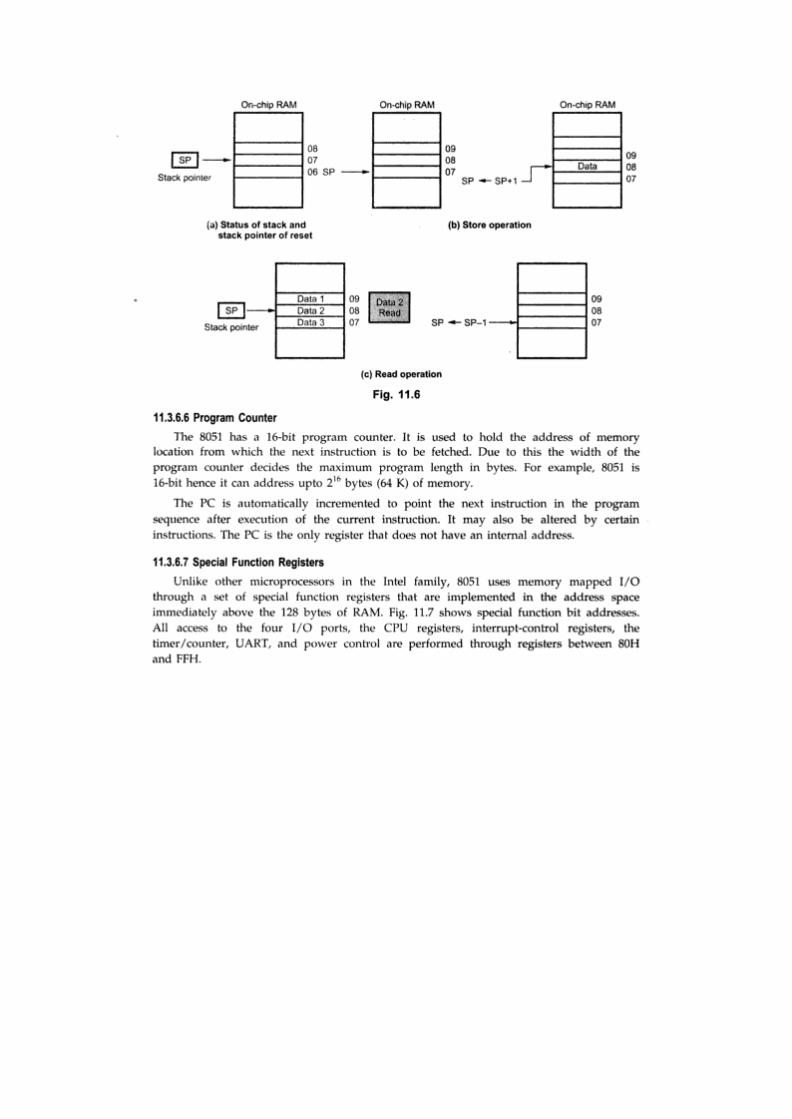
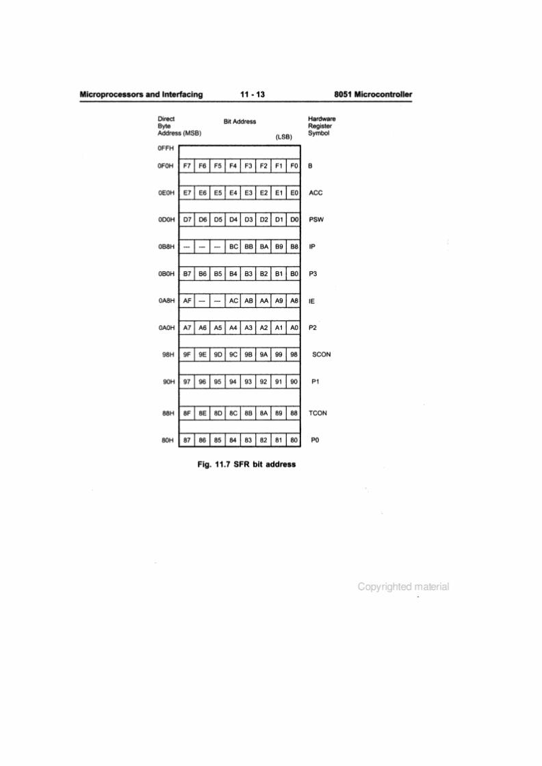
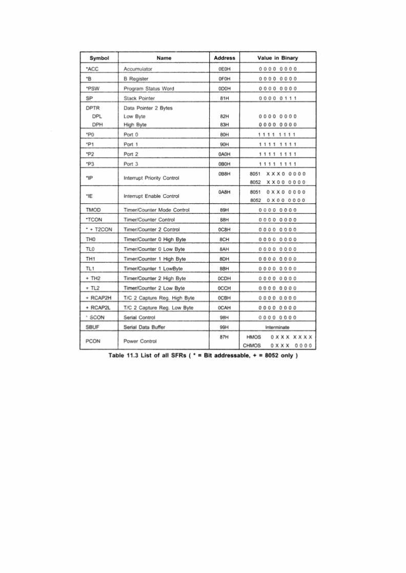
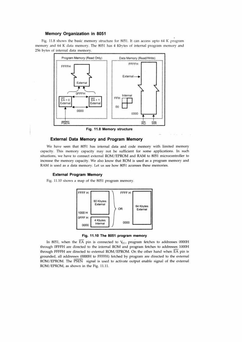

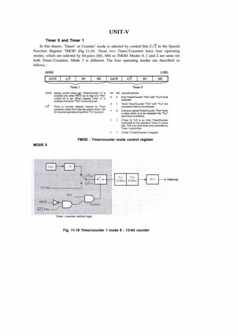
UNIT-V
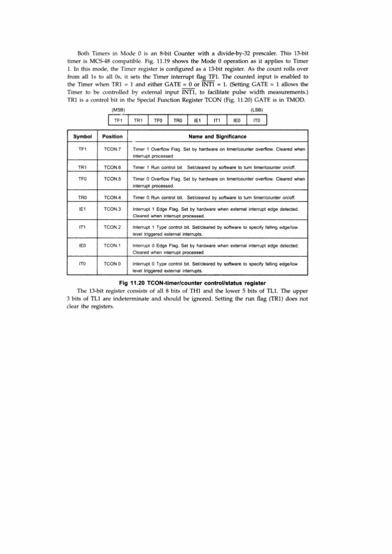
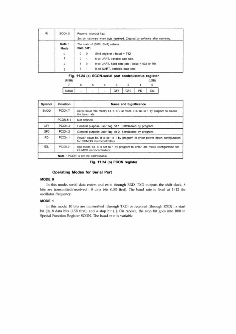
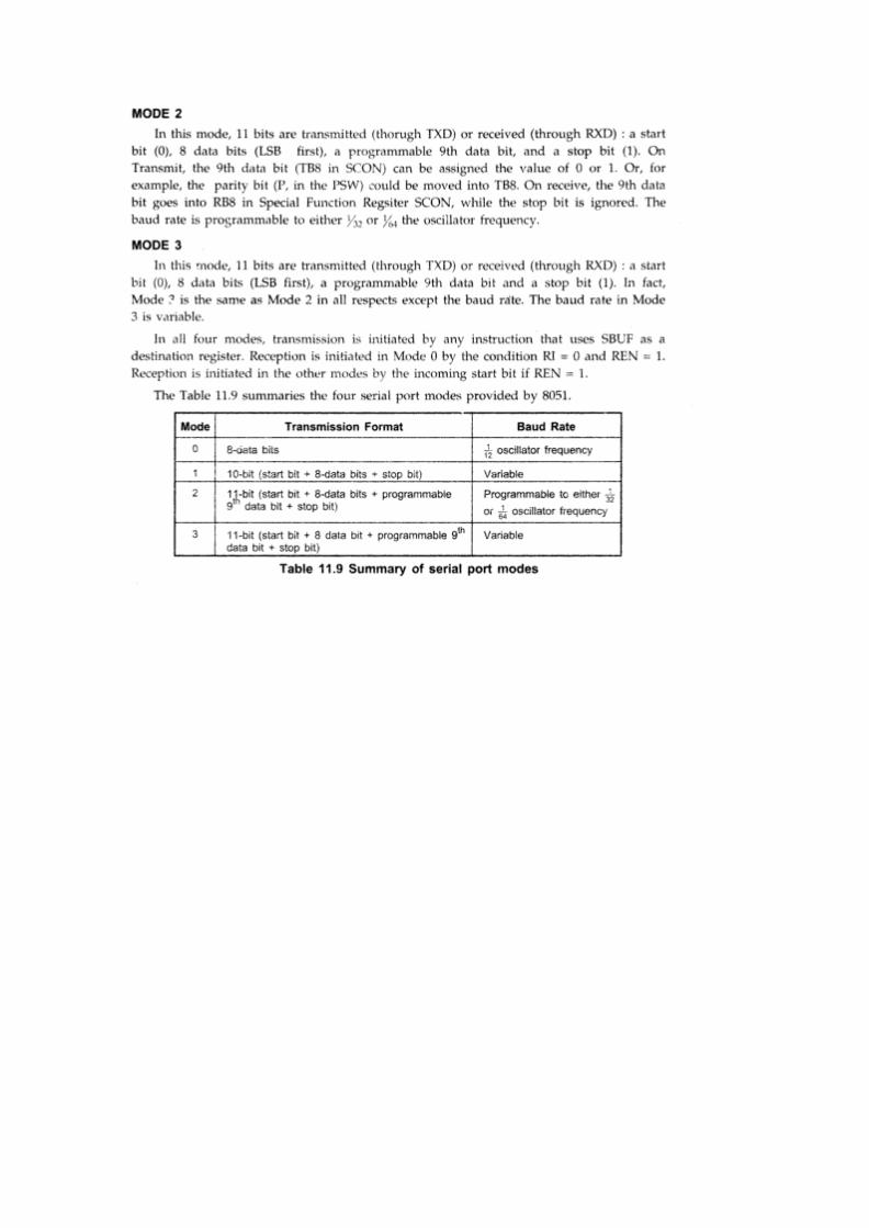

ADDITIONAL
15.ADDITIONAL TOPICS:
INTRODUCTION TO PENTIUM AND DUAL CORE PROCESSORS
DUAL CORE PROCESSORS
A multi-core processor is a single computing component with two or more
independent actual processors (called "cores"), which are the units that read and
execute program instructions.[1]
The instructions are ordinary CPU instructions such as add,
move data, and branch, but the multiple cores can run multiple instructions at the same time,
increasing overall speed for programs amenable to parallel. Manufacturers typically integrate
the cores onto a single integrated circuit die (known as a chip multiprocessor or CMP), or
onto multiple dies in a single chip package.
In which the number of cores is large enough that traditional multi-processor
techniques are no longer efficient— largely because of issues with congestion in supplying
instructions and data to the many processors. Processors were originally developed with only
one core. A many-core processor is a multi-core processor The many-core threshold is
roughly in the range of several tens of cores; above this threshold network on chip technology
is advantageous. Tilera processors feature a switch in each core to route data through an on-
chip mesh network to lessen the data congestion, enabling their core count to scale up to 100
cores.
A dual-core processor has two cores (e.g. AMD Phenom II X2, Intel Core Duo),
a quad-core processor contains four cores (e.g. AMD Phenom II X4, Intel's quad-core
processors, see i3, i5, and i7at Intel Core), a hexa-core processor contains six cores
(e.g. AMD Phenom II X6, Intel Core i7 Extreme Edition 980X), an octa-core
processor contains eight cores (e.g. Intel Xeon E7-2820, AMD FX-8150) A multi-core
processor implements multiprocessing in a single physical package. Designers may couple
cores in a multi-core device tightly or loosely. For example, cores may or may not
share caches, and they may implement message passing or shared memory inter-core
communication methods. Commonnetwork topologies to interconnect cores include bus, ring,
two-dimensional mesh, and crossbar.Homogeneous multi-core systems include only identical
cores, heterogeneous multi-core systems have cores that are not identical. Just as with single-
processor systems, cores in multi-core systems may implement architectures such
as superscalar, VLIW, vector processing, SIMD, or multithreading.
Multi-core processors are widely used across many application domains including general-
purpose,embedded, network, digital signal processing (DSP), and graphics.
Terminology
The terms multi-core and dual-core most commonly refer to some sort of central
processing unit (CPU), but are sometimes also applied todigital signal processors (DSP)
and system-on-a-chip (SoC circuit, unless otherwise noted. ). The terms are generally used
only to refer to multi-core microprocessors that are manufactured on the same integrated
circuit die; separate microprocessor dies in the same package are generally referred to by
another name, such as multi-chip module. This article uses the terms "multi-core" and "dual-
core" for CPUs manufactured on the same integrated circuits.
Commercial incentives
Several business motives drive the development of dual-core architectures. For
decades, it was possible to improve performance of a CPU by shrinking the area of the
integrated circuit, which drove down the cost per device on the IC. Alternatively, for the same
circuit area, more transistors could be utilized in the design, which increased functionality,
especially for CISC architectures. Clock rates also increased by orders of magnitude in the
decades of the late 20th century, from several megahertz in the 1980s to several gigahertz in
the early 2000s.
As the rate of clock speed improvements slowed, increased use of parallel computing
in the form of multi-core processors has been pursued to improve overall processing
performance. Multiple cores were used on the same CPU chip, which could then lead to
better sales of CPU chips with two or more cores. Intel has produced a 48-core processor for
research in cloud computing
Technical factors
Since computer manufacturers have long implemented symmetric
multiprocessing (SMP) designs using discrete CPUs, the issues regarding implementing
multi-core processor architecture and supporting it with software are well known.
Additionally:
Utilizing a proven processing-core design without architectural changes reduces design
risk significantly.
For general-purpose processors, much of the motivation for multi-core processors comes
from greatly diminished gains in processor performance from increasing the operating
frequency. This is due to three primary factors:
1. The memory wall; the increasing gap between processor and memory speeds.
This effect pushes cache sizes larger in order to mask the latency of memory.
This helps only to the extent that memory bandwidth is not the bottleneck in
performance.
2. The ILP wall; the increasing difficulty of finding enough parallelism in a single
instructions stream to keep a high-performance single-core processor busy.
3. The power wall; the trend of consuming exponentially increasing power with
each factorial increase of operating frequency. This increase can be mitigated by
"shrinking" the processor by using smaller traces for the same logic. The power
wall poses manufacturing, system design and deployment problems that have not
been justified in the face of the diminished gains in performance due to
the memory wall and ILP wall.

In order to continue delivering regular performance improvements for general-
purpose processors, manufacturers such as Intel and AMD have turned to multi-core designs,
sacrificing lower manufacturing-costs for higher performance in some applications and
systems. Multi-core architectures are being developed, but so are the alternatives. An
especially strong contender for established markets is the further integration of peripheral
functions into the chip.
The Pentium Dual-Core brand was used for mainstream x86
architecture microprocessors fromIntel from 2006 to 2009 when it was renamed to Pentium.
The processors are based on either the 32-bit Yonah or (with quite
different microarchitectures) 64-bit Merom-2M, Allendale, andWolfdale-3M core, targeted at
mobile or desktop computers.
In terms of features, price and performance at a given clock frequency, Pentium Dual-
Core processors were positioned above Celeron but below Core and Core 2 microprocessors
in Intel's product range. The Pentium Dual-Core was also a very popular choice for
overclocking, as it can deliver high performance (when overclocked) at a low price.
Processor cores
In 2006, Intel announced a plan[1]
to return the Pentium trademark from retirement to
the market, as a moniker of low-cost Core microarchitecture processors based on the single-
core Conroe-L but with 1 MiB of cache. The identification numbers for those
planned Pentiums were similar to the numbers of the latter Pentium Dual-
Core microprocessors, but with the first digit "1", instead of "2", suggesting their single-core
functionality. A single-core Conroe-L with 1 MiB cache was deemed as not strong enough to
distinguish the planned Pentiums from the Celerons, so it was replaced by dual-core CPUs,
adding "Dual-Core" to the line's name. Throughout 2009, Intel changed the name back from
Pentium Dual-Core to Pentium in its publications. Some processors were sold under both
names, but the newer E5400 through E6800 desktop and SU4100/T4x00 mobile processors
were not officially part of the Pentium Dual-Core line.
Comparison to the Pentium D
Although using the Pentium name, the desktop Pentium Dual-Core is based on the Core
microarchitecture, which can clearly be seen when comparing the specification to
the Pentium D, which is based on the NetBurst microarchitecture first introduced in the
Pentium 4. Below the 2 or 4 MiB of shared-L2-cache-enabled Core 2 Duo, the desktop
Pentium Dual-Core has 1 or 2 MiB of shared L2 Cache. In contrast, the Pentium D processors
have either 2 or 4 MiB of non-shared L2 cache. Additionally, the fastest-clocked Pentium D
has a factory boundary of 3.73 GHz, while the fastest-clocked desktop Pentium Dual-Core
reaches 3.2 GHz. A major difference among these processors is that the desktop Pentium
Dual Core processors have a TDP of only 65 W while the Pentium D ranges between 95 to
130 W. Despite the reduced clock speed, and lower amounts of cache, Pentium dual-core
outperfomed Pentium D by a fairly large margin.
Advantages
The proximity of multiple CPU cores on the same die allows the cache coherency circuitry to
operate at a much higher clock-rate than is possible if the signals have to travel off-chip.
Combining equivalent CPUs on a single die significantly improves the performance of cache
snoop (alternative: Bus snooping) operations. Put simply, this means that signals between
different CPUs travel shorter distances, and therefore those signals degrade less. These
higher-quality signals allow more data to be sent in a given time period, since individual
signals can be shorter and do not need to be repeated as often.The largest boost in
performance will likely be noticed in improved response-time while running CPU-intensive
processes, like antivirus scans, ripping/burning media (requiring file conversion), or file
searching. For example, if the automatic virus-scan runs while a movie is being watched, the
application running the movie is far less likely to be starved of processor power, as the
antivirus program will be assigned to a different processor core than the one running the
movie playback.
Assuming that the die can fit into the package, physically, the multi-core CPU designs require
much less printed circuit board (PCB) space than do multi-chip SMP designs. Also, a dual-
core processor uses slightly less power than two coupled single-core processors, principally
because of the decreased power required to drive signals external to the chip. Furthermore,
the cores share some circuitry, like the L2 cache and the interface to the front side bus (FSB).
In terms of competing technologies for the available silicon die area, multi-core design can
make use of proven CPU core library designs and produce a product with lower risk of design
error than devising a new wider core-design. Also, adding more cache suffers from
diminishing returns.[citation needed]
Multi-core chips also allow higher performance at lower energy. This can be a big factor in
mobile devices that operate on batteries. Since each core in multi-core is generally more
energy-efficient, the chip becomes more efficient than having a single large monolithic core.
This allows higher performance with less energy. The challenge of writing parallel code
clearly offsets this benefit.[4]
Disadvantages
Maximizing the utilization of the computing resources provided by multi-core
processors requires adjustments both to the operating system(OS) support and to existing
application software. Also, the ability of multi-core processors to increase application
performance depends on the use of multiple threads within applications. The situation is
improving: for example the Valve Corporation's Source engine offers multi-core
support,[5][6]
and Crytek has developed similar technologies for CryEngine 2, which powers
their game, Crysis. Emergent Game Technologies' Gamebryo engine includes their Floodgate
technology,[7]
which simplifies multicore development across game platforms. In
addition, Apple Inc.'s second latest OS, Mac OS X Snow Leopard has a built-in multi-core
facility called Grand Central Dispatch for Intel CPUs.
Integration of a multi-core chip drives chip production yields down and they are more
difficult to manage thermally than lower-density single-chip designs. Intel has partially
countered this first problem by creating its quad-core designs by combining two dual-core on
a single die with a unified cache, hence any two working dual-core dies can be used, as
opposed to producing four cores on a single die and requiring all four to work to produce a
quad-core. From an architectural point of view, ultimately, single CPU designs may make
better use of the silicon surface area than multiprocessing cores, so a development
commitment to this architecture may carry the risk of obsolescence. Finally, raw processing

power is not the only constraint on system performance. Two processing cores sharing the
same system bus and memory bandwidth limits the real-world performance advantage. If a
single core is close to being memory-bandwidth limited, going to dual-core might only give
30% to 70% improvement. If memory bandwidth is not a problem, a 90% improvement can
be expected[citation needed]
. It would be possible for an application that used two CPUs to end up
running faster on one dual-core if communication between the CPUs was the limiting factor,
which would count as more than 100% improvement.
Hardware
Trends
The general trend in processor development has moved from dual-, tri-, quad-, hexa-, octo-
core chips to ones with tens or even hundreds of cores. In addition, multi-core chips mixed
with simultaneous multithreading, memory-on-chip, and special-
purpose "heterogeneous" cores promise further performance and efficiency gains, especially
in processing multimedia, recognition and networking applications. There is also a trend of
improving energy-efficiency by focusing on performance-per-watt with advanced fine-grain
or ultra fine-grain power management and dynamic voltage and frequency
scaling (i.e. laptop computers and portable media players).
Architecture
The composition and balance of the cores in multi-core architecture show great variety. Some
architectures use one core design repeated consistently ("homogeneous"), while others use a
mixture of different cores, each optimized for a different, "heterogeneous" role.
The article "CPU designers debate multi-core future" by Rick Merritt, EE Times
2008,[8]
includes these comments:
Chuck Moore suggested computers should be more like cellphones, using a variety of
specialty cores to run modular software scheduled by a high-level applications programming
interface.
Atsushi Hasegawa, a senior chief engineer at Renesas, generally agreed. He suggested the
cellphone's use of many specialty cores working in concert is a good model for future multi-
core designs.
Anant Agarwal, founder and chief executive of startup Tilera, took the opposing view. He
said multi-core chips need to be homogeneous collections of general-purpose cores to keep
the software model simple.
Managing concurrency acquires a central role in developing parallel applications. The basic
steps in designing parallel applications are:
Partitioning
The partitioning stage of a design is intended to expose opportunities for parallel
execution. Hence, the focus is on defining a large number of small tasks in order to
yield what is termed a fine-grained decomposition of a problem.
Communication
The tasks generated by a partition are intended to execute concurrently but cannot, in
general, execute independently. The computation to be performed in one task will
typically require data associated with another task. Data must then be transferred
between tasks so as to allow computation to proceed. This information flow is
specified in the communication phase of a design.
Agglomeration
In the third stage, development moves from the abstract toward the concrete.
Developers revisit decisions made in the partitioning and communication phases with
a view to obtaining an algorithm that will execute efficiently on some class of parallel
computer. In particular, developers consider whether it is useful to combine, or
agglomerate, tasks identified by the partitioning phase, so as to provide a smaller
number of tasks, each of greater size. They also determine whether it is worthwhile to
replicate data and/or computation.
Mapping
In the fourth and final stage of the design of parallel algorithms, the developers
specify where each task is to execute. This mapping problem does not arise on
uniprocessors or on shared-memory computers that provide automatic task
scheduling.
On the other hand, on the server side, multicore processors are ideal because they allow many
users to connect to a site simultaneously and have independent threads of execution. This
allows for Web servers and application servers that have much better throughput.
PENTIUM PROCESSORS
Pentium is a brand used for a series of x86-compatible microprocessors produced by Intel. In
its most current form, a Pentium processor is a consumer-level product with a two-star
rating[1]
, above the low-end Atom and Celeron products but below the faster Core i3, i5 and
i7 lines as well as the high-end Xeon processors.
The name Pentium is originally derived from the Greek word pente (πέντε), meaning 'five' (as
the series was Intel's 5th generation microarchitecture, the P5), and the Latin ending -ium.
The current Pentium processors only share the name but are in fact based on the same
processor chips that are used in the Intel Core but are typically used with a lower clock
frequency, a partially disabled L3 cache and some of the advanced features such as Hyper-
threading andVirtualization disabled.
Overview
During development Intel generally identifies processors with codenames, such
as Prescott,Willamette, Coppermine, Katmai, Klamath or Deschutes. These usually become
widely known,] even after the processors are given official names on launch.
History
The original Pentium branded CPUs were expected to be named 586 or i586, to follow the
naming convention of previous generations (286,i386, i486). However, as the company
wanted to prevent their competitors from branding their processors with similar names, as
AMD had done with their Am486, Intel attempted to file a trademark on the name in the
United States, only to be denied because a series of numbers was not considered distinct.
Following Intel's previous series of 8086, 80186, 80286, 80386, and 80486 microprocessors,
the company's first P5-based processor was released as the original Intel Pentium on March
22, 1993. Due to its success, the Pentium brand would continue through several generations
of high-end processors beyond the original. In 2006, the Pentium brand briefly disappeared
from Intel's roadmaps,[3][4]
only to re-emerge in 2007.[5]
In 1998, Intel introduced the Celeron[6]
brand for low-priced microprocessors. With the 2006
introduction of the Intel Core brand as the company's new flagship line of processors, the
Pentium series was to be discontinued. However, due to a demand for mid-range dual-core
processors, the Pentium brand was re-purposed to be Intel's mid-range processor series, in
between the Celeron and Core series, continuing with the Pentium Dual-Core line.[7]
[8][9]
In 2009, the "Dual-Core" suffix was dropped, and new x86 microprocessors started carrying
the plain Pentium name again.
Pentium-branded processors
P5 microarchitecture based
The original Pentium and Pentium MMX processors were the superscalar follow-on to
the 80486 processor and were marketed from 1993 to 1999. Some versions of these were
available as Pentium OverDrive that would fit into older CPU sockets.
Pentium
P6 microarchitecture based
In parallel with the P5 microarchitecture, Intel developed the P6 microarchitecture and
started marketing it as the Pentium Pro for the high-end market in 1995. It introduced out-of-
order execution and an integrated second level cache on dual-chip processor package. The
second P6 generation replaced the original P5 with the Pentium II and rebranded the high-
end version as Pentium II Xeon. It was followed by a third version called the Pentium
III and Pentium III Xeon, respectively. The Pentium II line added the MMX instructions
that were also present in the Pentium MMX.
Versions of these processors for the Laptop market were initially called Mobile Pentium
II and Mobile Pentium III, later versions were called Pentium III-M. Starting with the
Pentium II, the Celeron brand was used for low-end versions of most Pentium processors
with a reduced feature set such as a smaller cache or missing power management features.
Pentium Pro
Pentium II
Pentium III
Netburst microarchitecture based
In 2000, Intel introduced a new microarchitecture called NetBurst, with a much longer
pipeline enabling higher clock frequencies than the P6 based processors. Initially, these were
called Pentium 4 and the high-end versions have since been called just Xeon. As with
Pentium III, there are both Mobile Pentium 4 and Pentium 4 M processors for the laptop
market, with Pentium 4 M denoting the more power-efficient versions. Enthusiasts version of
the Pentium 4 with the highest clock frequency were called Pentium 4 Extreme Edition.
The Pentium D was the first multi-core Pentium, integrating two Pentium 4 chips in one
package and was also available as the enthusiastPentium Extreme Edition.
Pentium 4
Pentium D
[Pentium M microarchitecture based
In 2003, Intel introduced a new processor based on the P6 microarchitecture called Pentium
M, which was much more power efficient than the Mobile Pentium 4, Pentium 4 M and
Pentium III M. Dual-core version of the Pentium M was developed under the code
name Yonah and sold under the marketing names Core Duo and Pentium Dual-Core. Unlike
Pentium D, it integrated both cores on a single chip. From this point, the Intel Core brand
name was used for the mainstream Intel processors and the Pentium brand became a low-end
version between Celeron and Core. All Pentium M based designs including Yonah are for the
mobile market.
Pentium M
Pentium Dual-Core
Core microarchitecture based
The Pentium Dual-Core name continued to be used when the Yonah design was extended
with 64 bit support, now called the Core microarchitecture. This microarchitecture
eventually replaced all NetBurst based processors across the four brands, Celeron, Pentium,
Core and Xeon. Pentium Dual-Core processors based on the Core microarchitecture use
the Allendale and Wolfdale-3M designs for desktop processors and Merom-2M for mobile
processors.
Pentium Dual-Core
Pentium (2009)
In 2009, Intel changed the naming system for Pentium processors, renaming the Wolfdale-3M
based processors to Pentium, without the Dual-Core name and introduced new single- and
dual-core processors based on Penryn under the Pentium name.
The Penryn core is the successor to the Merom core and Intel's 45 nm version of their mobile
series of Pentium microprocessors. The FSB is increased from 667 MHz to 800 MHz and the
voltage is lowered. Intel released the first Penryn Core, the Pentium T4200, in December,
2008. In June 2009, Intel released the first single-core processor to use the Pentium name,
a Consumer Ultra-Low Voltage (CULV) Penryn core called the Pentium SU2700.
In September 2009, Intel introduced the Pentium SU4000 series together with the Celeron
SU2000 and Core 2 Duo SU7000 series, which are dual-core CULV processors based on
Penryn-3M and using 800 MHz FSB. The Pentium SU4000 series has 2 MB L2 cache but is
otherwise basically identical to the other two lines.
Nehalem microarchitecture based
The Nehalem microarchitecture was introduced in late 2008 as a successor to the Core
microarchitecture, and in early 2010, a new PentiumG6950 processor based on
the Clarkdale design was introduced based on the Westmere refresh of Nehalem, which
were followed by the mobile P6xxx based on Arrandale a few months later.
On January 7, 2010, Intel launched a new Pentium model using the Clarkdale chip in parallel
with other desktop and mobile CPUs based on their new Westmere microarchitecture. The
first model in this series is the Pentium G6950. The Clarkdale chip is also used in the Core i3-
5xx and Core i5-6xx series and features a 32 nm process (as it is based on the Westmere
microarchitecture), integrated memory controller and 45 nm graphics controller and a third-
level cache. In the Pentium series, some features of Clarkdale are disabled. Compared to Core
i3, it lacks Hyper-Threading and the graphics controller in the Pentium runs at 533 MHz,
while in the Core i3 i3-5xx series they run at 733 MHz. Dual Video Decode that enables Blu-
ray picture-in picture hardware acceleration is disabled as well as Deep Color
and xvYCCsupport]. The memory controller in the Pentium supports DDR3-1066 max same
as the Core i3 i3-5xx series (ref:http://ark.intel.com/products/43529). The L3 cache is also 1
MB less than in the Core i3-5xx series.
Sandy Bridge microarchitecture based
The Sandy Bridge microarchitecture was released in the Pentium line on May 22, 2011.
aAll models share the following details: 2 cores, 2 logical processors (4 on Pentium 3xx
with Hyper-threading), CPUID signature 206A7, family 6 (06h), model 42 (02Ah),
stepping 7 (07h)
bTLB / cache 64-byte Prefetching; Data TLB0 2-MB or 4-MB pages, 4-way associative,
32 entries; Data TLB 4-KB Pages, 4-way set associative, 64 entries; Instruction TLB 4-
KB Pages, 4-way set associative, 128 entries, L2 TLB 1-MB, 4-way set associative, 64-
byte line size; Shared 2nd-level TLB 4 KB pages, 4-way set associative, 512 entries.
cAll models feature: On-chip Floating Point Unit, Enhanced Intel SpeedStep Technology
(EIST), Intel 64, XD bit (an NX bitimplementation), Intel VT-x, Smart Cache.
dAll models support: MMX, SSE, SSE2, SSE3, SSSE3, SSE4.1, SSE4.2
eHD Graphics (Sandy Bridge) contain 6 EUs as well as HD Graphics 2000, but does not
support the following technologies: Intel Quick Sync Video, InTru 3D, Clear Video HD,
Wireless Display, and it doesn't support 3D Video or 3D graphics acceleration.
Pentium compatible Intel processors
Due to its prominence, the term "Pentium compatible" is often used to describe any x86
processor that supports the IA-32 instruction set and architecture. Even though they do not
use the Pentium name, Intel also manufacturers other processors based on the Pentium series
for other markets. Most of these processors share the core design with one of the Pentium
processor lines, usually differing in the amount ofCPU cache, power efficiency or other
features. The notable exception is the Atom line, which is an independent design.
Celeron, a low-end version
Core, the mainstream version including Core 2 and Core i7, now placed above Pentium
Xeon, a high-end version used in servers and workstations
A100 (discontinued), an ultra-mobile version of Pentium M
EP80579, A system-on-a-chip based on Pentium M
Atom, current ultra-mobile processors
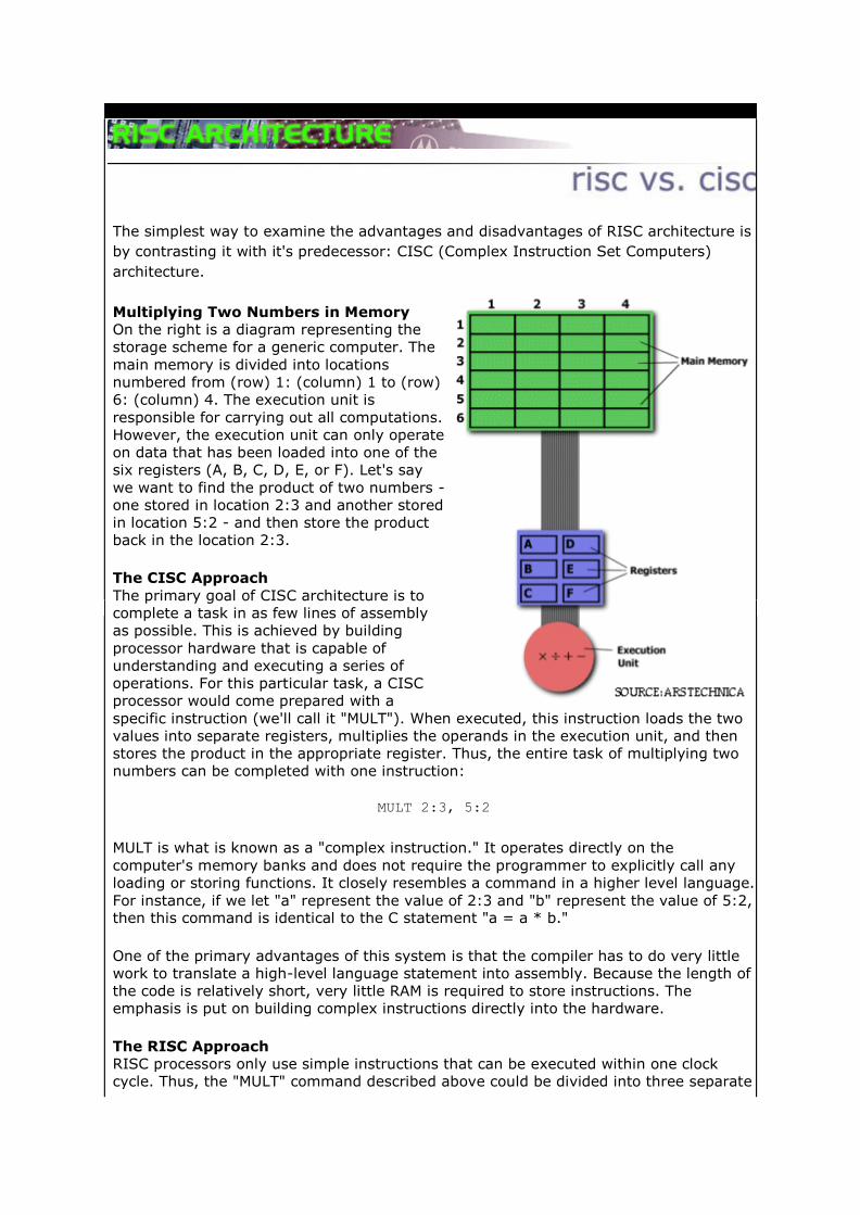
The simplest way to examine the advantages and disadvantages of RISC architecture is
by contrasting it with it's predecessor: CISC (Complex Instruction Set Computers)
architecture.
Multiplying Two Numbers in Memory
On the right is a diagram representing the
storage scheme for a generic computer. The
main memory is divided into locations
numbered from (row) 1: (column) 1 to (row)
6: (column) 4. The execution unit is
responsible for carrying out all computations.
However, the execution unit can only operate
on data that has been loaded into one of the
six registers (A, B, C, D, E, or F). Let's say
we want to find the product of two numbers -
one stored in location 2:3 and another stored
in location 5:2 - and then store the product
back in the location 2:3.
The CISC Approach
The primary goal of CISC architecture is to
complete a task in as few lines of assembly
as possible. This is achieved by building
processor hardware that is capable of
understanding and executing a series of
operations. For this particular task, a CISC
processor would come prepared with a
specific instruction (we'll call it "MULT"). When executed, this instruction loads the two
values into separate registers, multiplies the operands in the execution unit, and then
stores the product in the appropriate register. Thus, the entire task of multiplying two
numbers can be completed with one instruction:
MULT 2:3, 5:2
MULT is what is known as a "complex instruction." It operates directly on the
computer's memory banks and does not require the programmer to explicitly call any
loading or storing functions. It closely resembles a command in a higher level language.
For instance, if we let "a" represent the value of 2:3 and "b" represent the value of 5:2, then this command is identical to the C statement "a = a * b."
One of the primary advantages of this system is that the compiler has to do very little
work to translate a high-level language statement into assembly. Because the length of
the code is relatively short, very little RAM is required to store instructions. The
emphasis is put on building complex instructions directly into the hardware.
The RISC Approach
RISC processors only use simple instructions that can be executed within one clock
cycle. Thus, the "MULT" command described above could be divided into three separate
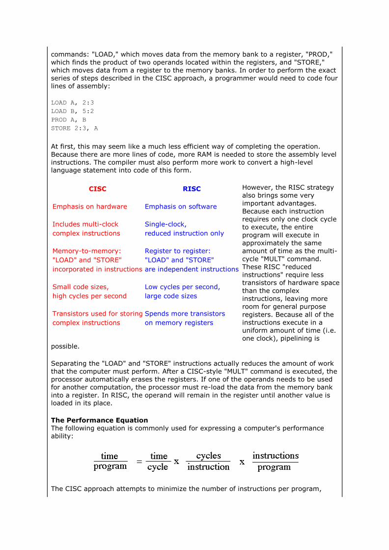
commands: "LOAD," which moves data from the memory bank to a register, "PROD,"
which finds the product of two operands located within the registers, and "STORE,"
which moves data from a register to the memory banks. In order to perform the exact
series of steps described in the CISC approach, a programmer would need to code four lines of assembly:
LOAD A, 2:3
LOAD B, 5:2
PROD A, B
STORE 2:3, A
At first, this may seem like a much less efficient way of completing the operation.
Because there are more lines of code, more RAM is needed to store the assembly level
instructions. The compiler must also perform more work to convert a high-level language statement into code of this form.
However, the RISC strategy
also brings some very
important advantages.
Because each instruction
requires only one clock cycle
to execute, the entire
program will execute in
approximately the same
amount of time as the multi-
cycle "MULT" command.
These RISC "reduced
instructions" require less
transistors of hardware space
than the complex
instructions, leaving more
room for general purpose
registers. Because all of the
instructions execute in a
uniform amount of time (i.e.
one clock), pipelining is
possible.
Separating the "LOAD" and "STORE" instructions actually reduces the amount of work
that the computer must perform. After a CISC-style "MULT" command is executed, the
processor automatically erases the registers. If one of the operands needs to be used
for another computation, the processor must re-load the data from the memory bank
into a register. In RISC, the operand will remain in the register until another value is loaded in its place.
The Performance Equation
The following equation is commonly used for expressing a computer's performance ability:
The CISC approach attempts to minimize the number of instructions per program,
CISC RISC
Emphasis on hardware Emphasis on software
Includes multi-clock
complex instructions Single-clock,
reduced instruction only
Memory-to-memory:
"LOAD" and "STORE"
incorporated in instructions
Register to register:
"LOAD" and "STORE"
are independent instructions
Small code sizes,
high cycles per second Low cycles per second,
large code sizes
Transistors used for storing
complex instructions Spends more transistors
on memory registers
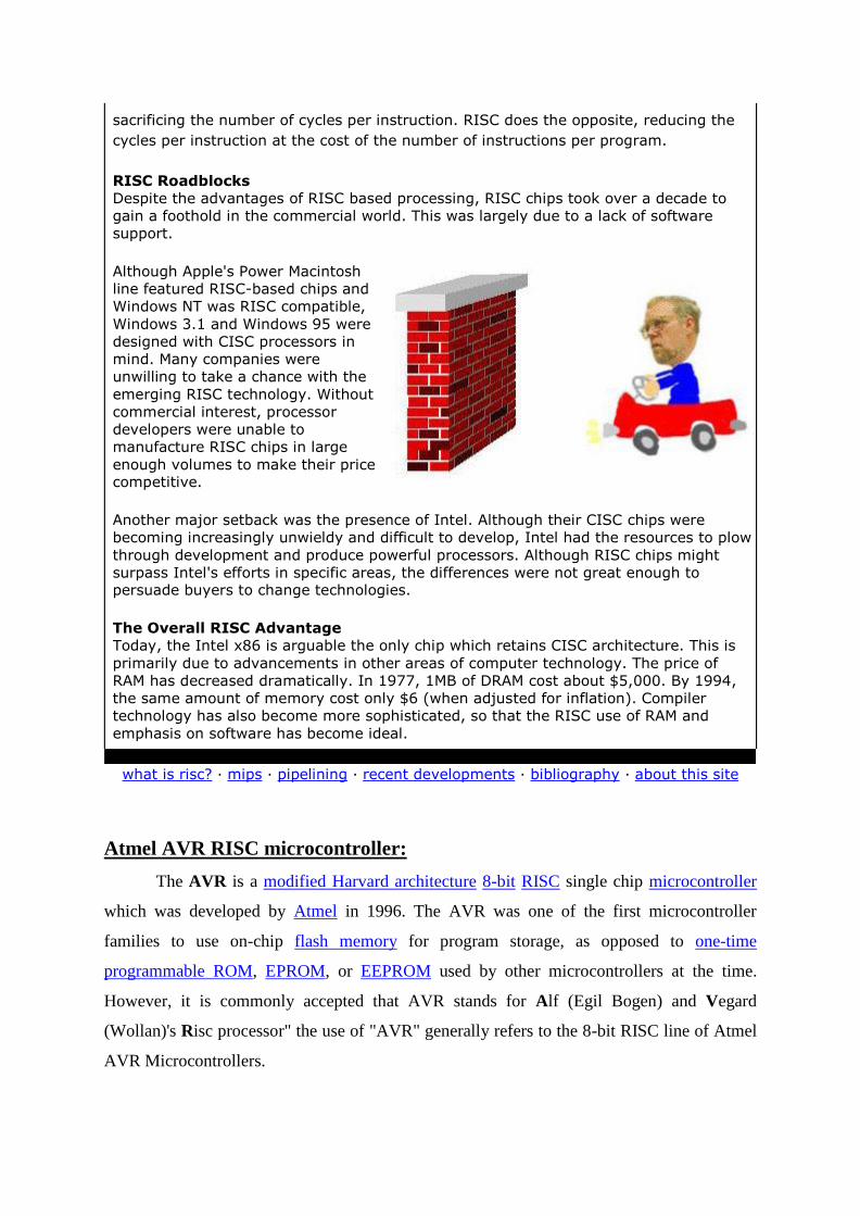
sacrificing the number of cycles per instruction. RISC does the opposite, reducing the
cycles per instruction at the cost of the number of instructions per program.
RISC Roadblocks
Despite the advantages of RISC based processing, RISC chips took over a decade to
gain a foothold in the commercial world. This was largely due to a lack of software
support.
Although Apple's Power Macintosh
line featured RISC-based chips and
Windows NT was RISC compatible,
Windows 3.1 and Windows 95 were
designed with CISC processors in
mind. Many companies were
unwilling to take a chance with the
emerging RISC technology. Without
commercial interest, processor
developers were unable to
manufacture RISC chips in large
enough volumes to make their price competitive.
Another major setback was the presence of Intel. Although their CISC chips were
becoming increasingly unwieldy and difficult to develop, Intel had the resources to plow
through development and produce powerful processors. Although RISC chips might
surpass Intel's efforts in specific areas, the differences were not great enough to persuade buyers to change technologies.
The Overall RISC Advantage
Today, the Intel x86 is arguable the only chip which retains CISC architecture. This is
primarily due to advancements in other areas of computer technology. The price of
RAM has decreased dramatically. In 1977, 1MB of DRAM cost about $5,000. By 1994,
the same amount of memory cost only $6 (when adjusted for inflation). Compiler
technology has also become more sophisticated, so that the RISC use of RAM and
emphasis on software has become ideal.
what is risc? · mips · pipelining · recent developments · bibliography · about this site
Atmel AVR RISC microcontroller:
The AVR is a modified Harvard architecture 8-bit RISC single chip microcontroller
which was developed by Atmel in 1996. The AVR was one of the first microcontroller
families to use on-chip flash memory for program storage, as opposed to one-time
programmable ROM, EPROM, or EEPROM used by other microcontrollers at the time.
However, it is commonly accepted that AVR stands for Alf (Egil Bogen) and Vegard
(Wollan)'s Risc processor" the use of "AVR" generally refers to the 8-bit RISC line of Atmel
AVR Microcontrollers.
Among the first of the AVR line was the AT90S8515, which in a 40-pin DIP package
has the same pinout as an 8051 microcontroller, including the external multiplexed address
and data bus. The polarity of the RESET line was opposite (8051's having an active-high
RESET, while the AVR has an active-low RESET) but other than that, the pinout was
identical.
overview
The AVR is a modified Harvard architecture machine where program and data are stored in
separate physical memory systems that appear in different address spaces, but having the
ability to read data items from program memory using special instructions.
Basic families
AVRs are generally classified into five broad groups:
tinyAVR — the ATtiny series
o 0.5–8 kB program memory
o 6–32-pin package
o Limited peripheral set
megaAVR — the ATmega series
o 4–256 kB program memory
o 28–100-pin package
o Extended instruction set (Multiply instructions and instructions for handling
larger program memories)
o Extensive peripheral set
XMEGA — the ATxmega series
o 16–384 kB program memory
o 44–64–100-pin package (A4, A3, A1)
o Extended performance features, such as DMA, "Event System", and
cryptography support.
o Extensive peripheral set with DACs
Application-specific AVR
o megaAVRs with special features not found on the other members of the AVR
family, such as LCD controller, USB controller, advanced PWM, CAN etc.
FPSLIC™ (AVR with FPGA)
o FPGA 5K to 40K gates
o SRAM for the AVR program code, unlike all other AVRs
o AVR core can run at up to 50 MHz [5]
32-bit AVRs
In 2006 Atmel released microcontrollers based on the new, 32-bit, AVR32
architecture. They include SIMD and DSP instructions, along with other audio and
video processing features. This 32-bit family of devices is intended to compete with
the ARM based processors. The instruction set is similar to other RISC cores, but is
not compatible with the original AVR or any of the various ARM cores.
Architecture
Flash, EEPROM, and SRAM are all integrated onto a single chip, removing the need
for external memory in most applications. Some devices have a parallel external bus option to
allow adding additional data memory or memory-mapped devices. Almost all devices (except
the smallest TinyAVR chips) have serial interfaces, which can be used to connect larger serial
EEPROMs or flash chips. The fast-access register file concept contains 32 x 8-bit general-
purpose working registers With a single clock cycle access time. This means that during one
single clock cycle, one Arithmetic Logic Unit (ALU)operation is executed. Two operands are
output from the register file, the operation is executed and the result is stored back in the
register file–in one clock cycle.
Six of the 32 registers can be used as three 16-bit indirect addresses register pointers for Data
Space addressing, enabling efficient address calculations. One of the three address pointers is
also used as the address pointer for the constant table look-up function.
These addedfunctionregistersarethe16-bitX-register, Y-register, and Z-register.
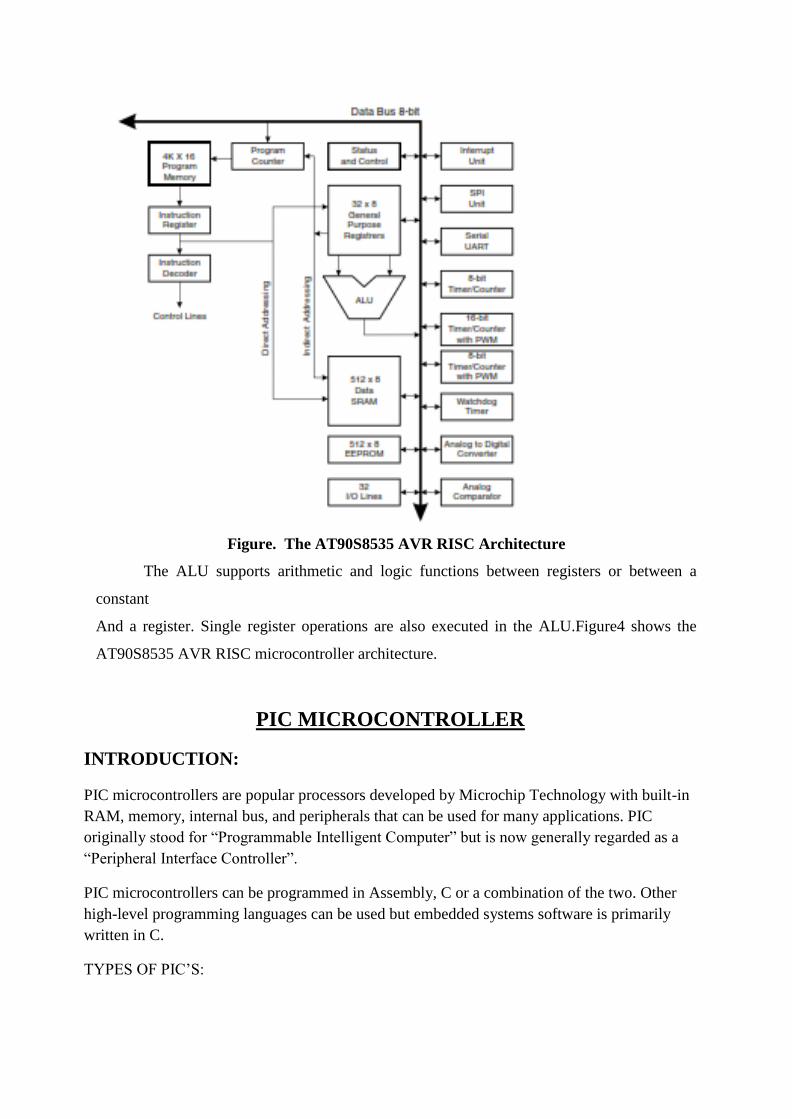
Figure. The AT90S8535 AVR RISC Architecture
The ALU supports arithmetic and logic functions between registers or between a
constant
And a register. Single register operations are also executed in the ALU.Figure4 shows the
AT90S8535 AVR RISC microcontroller architecture.
PIC MICROCONTROLLER
INTRODUCTION:
PIC microcontrollers are popular processors developed by Microchip Technology with built-in
RAM, memory, internal bus, and peripherals that can be used for many applications. PIC
originally stood for ―Programmable Intelligent Computer‖ but is now generally regarded as a
―Peripheral Interface Controller‖.
PIC microcontrollers can be programmed in Assembly, C or a combination of the two. Other
high-level programming languages can be used but embedded systems software is primarily
written in C.
TYPES OF PIC‘S:
PIC microcontrollers are broken up into two major categories: 8-bit microcontrollers and 16-bit
microcontrollers. Each category is further subdivided into product families as shown in the
following table:
8-bit MCU Product Family 16-bit MCU Product Family
PIC10
PIC12
PIC14
PIC16
PIC18
PIC24F
PIC24H
dsPIC30
dsPIC33
The microcontrollers in the PIC10 through PIC14 families are considered low-end
microcontrollers. PIC microcontrollers in the PIC16 and PIC18 families are considered mid-
level microcontrollers while 16-bit PICs are considered high-end microcontrollers.
FEATURES:
Family includes controllers from 16c61/62/64/71/74/710/715 etc.
They are RISC processors and uses Harvard architecture.
Different bus widths of data and program memory.
Data memory is 8 bit wide where as program memory is 12,14,16 bits wide.
The instruction holds immediate data along with instruction code.
Only 35 instructions.
Most instructions take 0.2 microseconds to execute when operated at 20 MHz.
Machine cycle consist of 4 clock pulses.
Instruction set is highly orthogonal.
1-3 Timers with 8/16 bit prescalar.
Watch Dog timer (WDT)
13-33 I/O pins.
3-12 interrupt Sources.
4/8 Channel, 8 bit on chip ADC.
Power on Reset. (POR)
Brown out Reset (BOR).
Capture/Compare/ PWM modules.
USART
Synchronous serial port (SSP) with SPI and I2C.
Power saving SLEEP mode.
Wide operating Voltage range 2.5 V to 6.0 V.Very Low power consumption.
Commercial,Industrial and Extended Temperature ranges.
Parallel slave port (PSP),8 bits wide with external RD,WR and CS controls.
PICs also come in several types of packages:
Plastic Dual Inline Package (PDIP),Small-Outline Transistor (SOT),Dual Flat No-lead
(DFN),Mini Small Outline Package (MSOP),Thin Quad Flat Pack (TQFP),Plastic Leaded Chip
Carrier (PLCC),CERamic QUADpack (CERQUAD),
The reason for the number of packages is that there are some PICs with 100 I/O pins! The
microcontrollers are basically rectangular or square shaped. The easiest package to work with is
DIP or PDIP because it is easily bread boardable and can easily be soldered.Writing your code
completely in C because it is much faster and easier than writing your code in Assembly or a
combination of languages.
PIC ARCHITECTURE:
ALU
Size is 8 bit Performs operations with temporary working register and (W register) and any
register file. W register 8 bit wide. It contains one of source operands during execution of
instruction and may serve as the destination for the result of operation. Used only for ALU
operations.
STATUS Register
7 6 5 4 3 2 1 0
0 0 RP0 T0 PD Z DC C
C = Carry Bit
DC = Digits Carry (Same as AC)
Z = Zero
TO = Reset status bit ( Time out bit)
PD = Reset status bit ( Power down)
These bits are used along with SLEEP mode. After coming out from SLEEP processor checks
these bits to determine which kind of event is responsible for bringing out of SLEEP mode.RP0
= Register Bank Select bit.If 0 selects bank 0 otherwise bank 1.
FSR Register (File Selection Register):
FSR is a pointer used for indirect memory addressing in the whole register file. In indirect
addressing mode one has to write address byte in FSR and then use INDF ( Indirect thro
FSR).INDF is used in instruction.
PCLATH (PC Latch):
Can be independently read or written like any other register.It‘s different from PC and is
separate entity. It is 5 bits.This is added with PCL (Program Counter Lower) so as to get 13 bit
address.
PROGRAM MEMORY
PIC 16c6X/7X is 2K or 4K.
11 bit or 12 bit address is used out of
13 bits in PC.
Maximum memory that can be accessed is 8K.
After reset program counter is cleared.
At 0000h there is ―goto Mainline‖ Instruction which takes PC to 0005h.
DATA MEMORY:
Register File Structure:They are the memory locations that are addressed Be instruction.There
is general purpose and special purpose register file.General purpose are 8 bit RAM locations
and special purpose are I/O ports and control registers.
ADDRESSING MODES:
Direct Addressing:
It uses 7 bits of instruction and the 8 bit from RP0.If bit is 0 then bank otherwise bank 1.
Indirect addressing
In this mode the 8 bit address of the location in register file to be accessed is written in FSR
and use INDF.
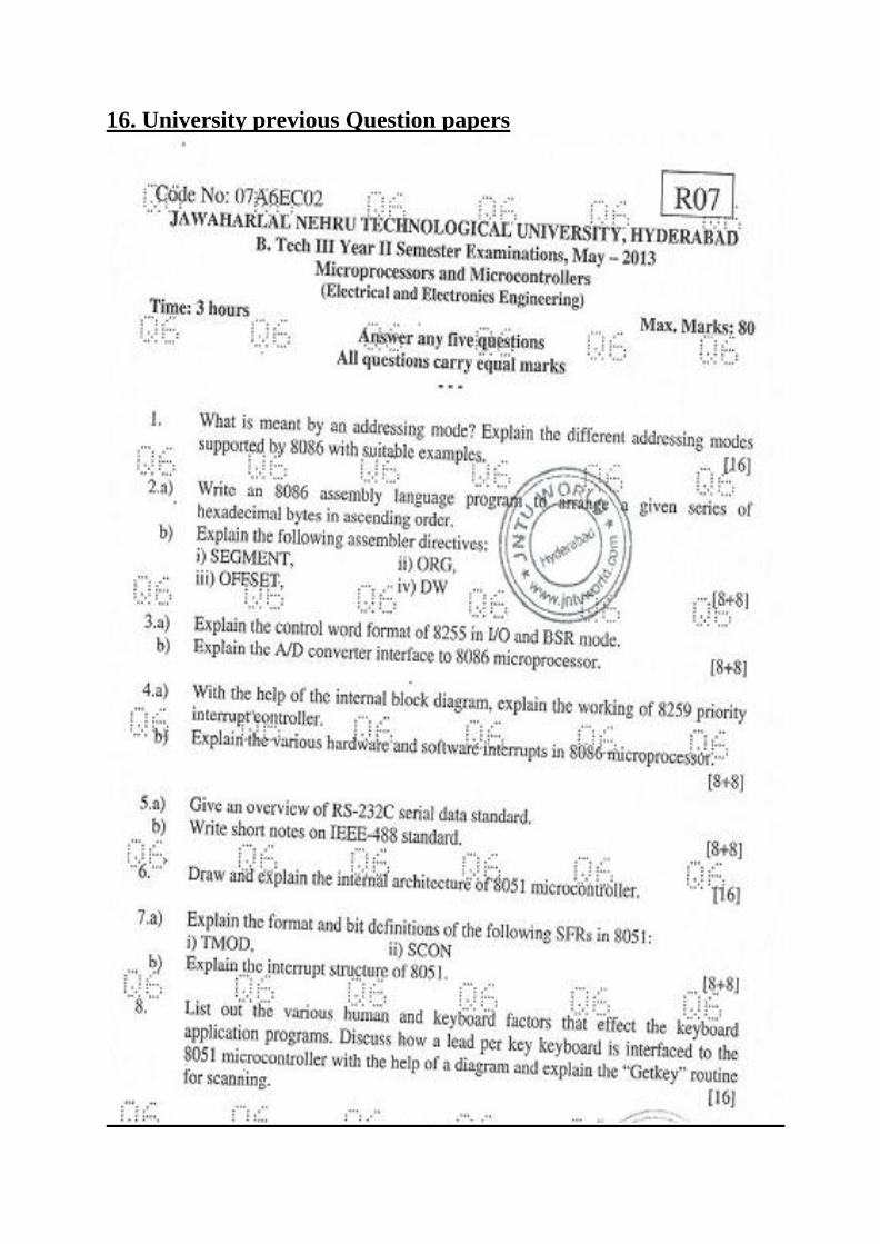
16. University previous Question papers
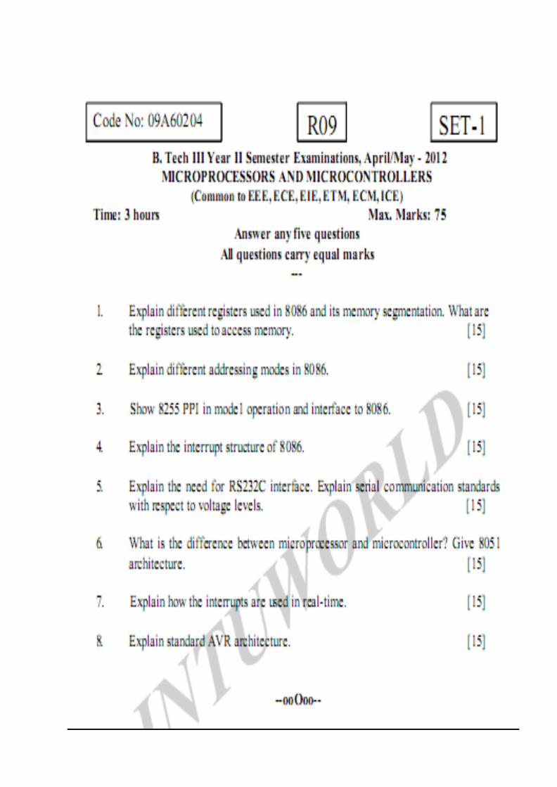
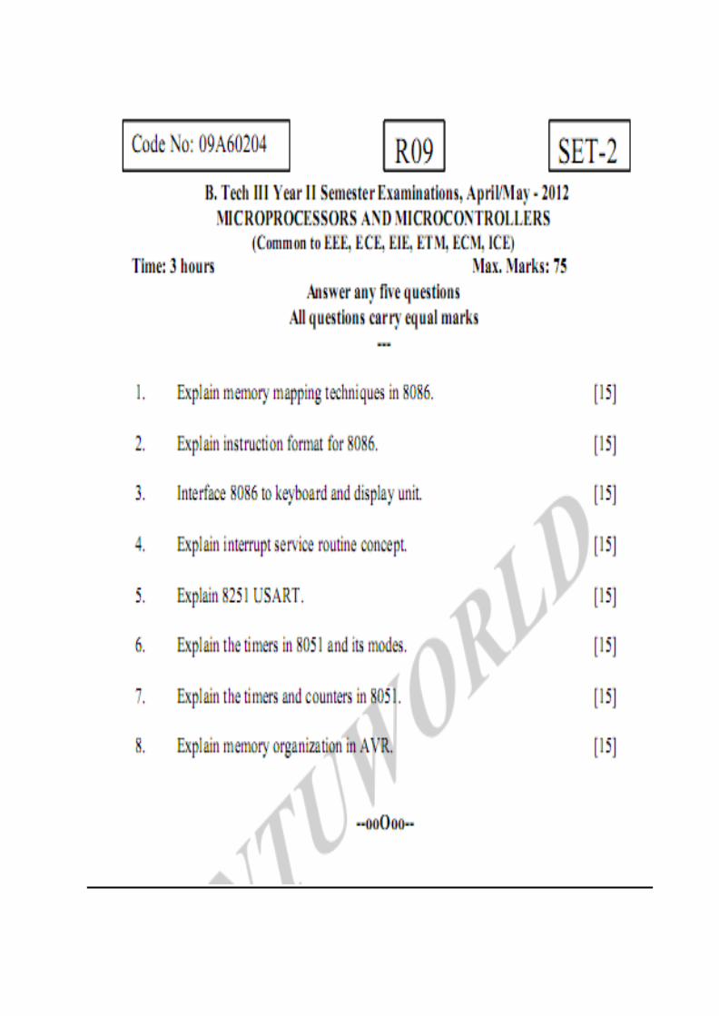
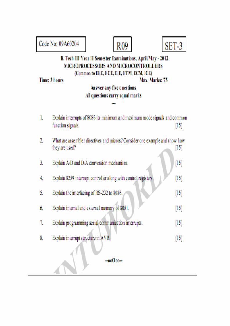
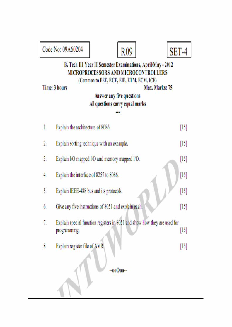


III B. Tech II Semester Regular Examinations, Apr/May 2010
MICROPROCESSORS AND INTERFACING (Common to ECE, BME, EIE)
Time: 3 Hours Max Marks: 80
Answer Any FIV Questions
All Questions Carry Equal Marks
1. a) Draw and explain the flag register of 8086 microprocessor.
b) Explain the different logical instructions of 8086 microprocessor. [8+8]
2. Write an assembly language program in 8086 to arrange the given series
of hexadecimal numbers in ascending order. [16]
3. With neat circuit diagram and timing diagrams, explain the minimum mode operation of 8086 microprocessor. [16]
4. Interface an 8255 with 8086 to work as an I/O port. Initialize port A as output port, port B as input port and port C as output port. Port A address should be 0740H.Write a program to sense switch positions SW0 –SW7
connected at port B. The sensed pattern is to be displayed in port A, to which 8 LEDs are connected, which the port C lower displays number of on switches out of the total eight switches. [16]
5. a) What is the difference between maskable and non-makeable interrupts?
Give some examples?
b) Discuss about the following control word formats of 8259:
i. Initialization Command Words (ICWs).
ii. Operational Command Words (OCWs) [6+10]
6. a) Discuss the types of serial communication.
b) With a neat circuit diagram, explain the interfacing of 8251 with 8086. [6+10]
7. a) What is meant by paging? Explain its advantages and disadvantages.
b) Explain the procedure of converting linear address into physical address. [8+8]
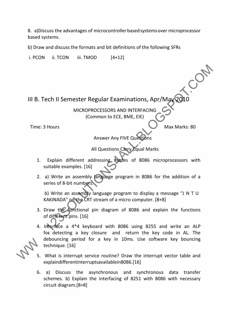
8. a)Discuss the advantages of microcontroller based systems over microprocessor based systems.
b) Draw and discuss the formats and bit definitions of the following SFRs
i. PCON ii. TCON iii. TMOD [4+12]
III B. Tech II Semester Regular Examinations, Apr/May 2010
MICROPROCESSORS AND INTERFACING (Common to ECE, BME, EIE)
Time: 3 Hours Max Marks: 80
Answer Any FIVE Questions
All Questions Carry Equal Marks
1. Explain different addressing modes of 8086 microprocessors with suitable examples. [16]
2. a) Write an assembly language program in 8086 for the addition of a series of 8-bit numbers.
b) Write an assembly language program to display a message “J N T U KAKINADA” on the CRT stream of a micro computer. [8+8]
3. Draw the functional pin diagram of 8086 and explain the functions of different pins. [16]
4. Interface a 4*4 keyboard with 8086 using 8255 and write an ALP for detecting a key closure and return the key code in AL. The debouncing period for a key in 10ms. Use software key bouncing technique. [16]
5. What is interrupt service routine? Draw the interrupt vector table and explaindifferentinterruptsavailablein8086.[16]
6. a) Discuss the asynchronous and synchronous data transfer schemes. b) Explain the interfacing of 8251 with 8086 with necessary circuit diagram.[8+8]
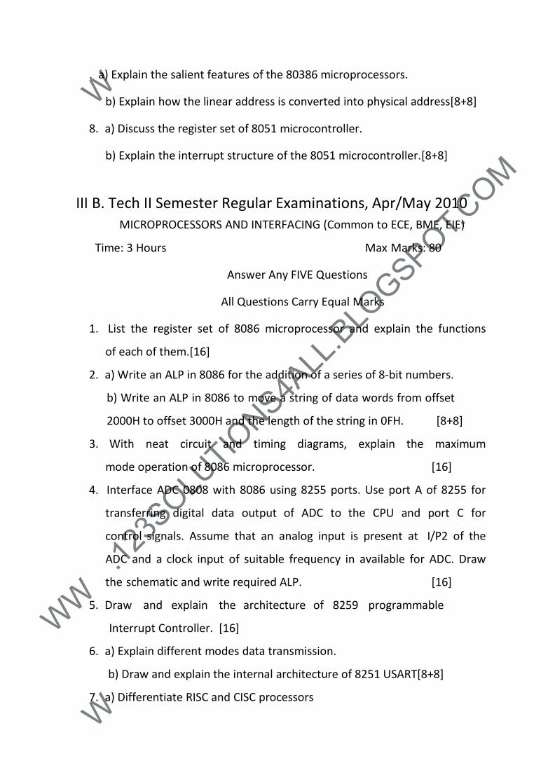
. a) Explain the salient features of the 80386 microprocessors.
b) Explain how the linear address is converted into physical address[8+8]
8. a) Discuss the register set of 8051 microcontroller.
b) Explain the interrupt structure of the 8051 microcontroller.[8+8]
III B. Tech II Semester Regular Examinations, Apr/May 2010
MICROPROCESSORS AND INTERFACING (Common to ECE, BME, EIE)
Time: 3 Hours Max Marks: 80
Answer Any FIVE Questions
All Questions Carry Equal Marks
1. List the register set of 8086 microprocessor and explain the functions
of each of them.[16]
2. a) Write an ALP in 8086 for the addition of a series of 8-bit numbers.
b) Write an ALP in 8086 to move a string of data words from offset
2000H to offset 3000H and the length of the string in 0FH. [8+8]
3. With neat circuit and timing diagrams, explain the maximum
mode operation of 8086 microprocessor. [16]
4. Interface ADC 0808 with 8086 using 8255 ports. Use port A of 8255 for
transferring digital data output of ADC to the CPU and port C for
control signals. Assume that an analog input is present at I/P2 of the
ADC and a clock input of suitable frequency in available for ADC. Draw
the schematic and write required ALP. [16]
5. Draw and explain the architecture of 8259 programmable
Interrupt Controller. [16]
6. a) Explain different modes data transmission.
b) Draw and explain the internal architecture of 8251 USART[8+8]
7. a) Differentiate RISC and CISC processors
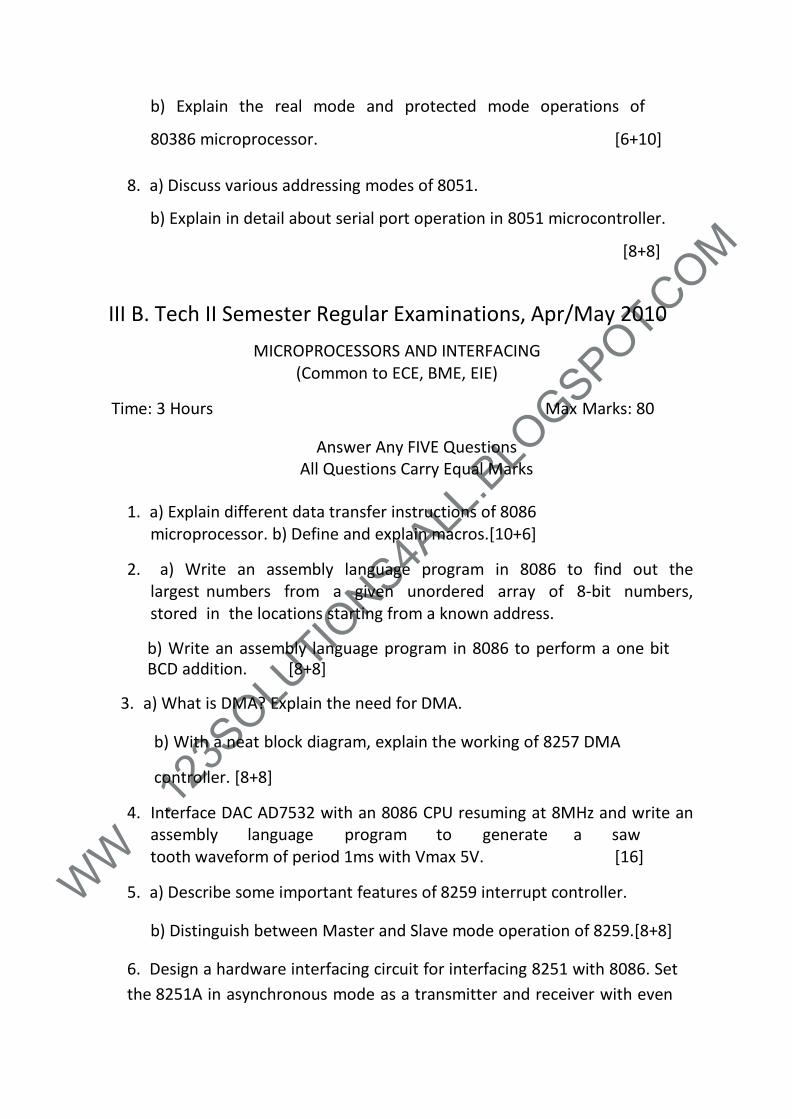
b) Explain the real mode and protected mode operations of
80386 microprocessor. [6+10]
8. a) Discuss various addressing modes of 8051.
b) Explain in detail about serial port operation in 8051 microcontroller.
[8+8]
III B. Tech II Semester Regular Examinations, Apr/May 2010
MICROPROCESSORS AND INTERFACING (Common to ECE, BME, EIE)
Time: 3 Hours Max Marks: 80
Answer Any FIVE Questions All Questions Carry Equal Marks
1. a) Explain different data transfer instructions of 8086
microprocessor. b) Define and explain macros.[10+6]
2. a) Write an assembly language program in 8086 to find out the largest numbers from a given unordered array of 8-bit numbers, stored in the locations starting from a known address.
b) Write an assembly language program in 8086 to perform a one bit BCD addition. [8+8]
3. a) What is DMA? Explain the need for DMA.
b) With a neat block diagram, explain the working of 8257 DMA
controller. [8+8]
4. Interface DAC AD7532 with an 8086 CPU resuming at 8MHz and write an assembly language program to generate a saw tooth waveform of period 1ms with Vmax 5V. [16]
5. a) Describe some important features of 8259 interrupt controller.
b) Distinguish between Master and Slave mode operation of 8259.[8+8]
6. Design a hardware interfacing circuit for interfacing 8251 with 8086. Set
the 8251A in asynchronous mode as a transmitter and receiver with even
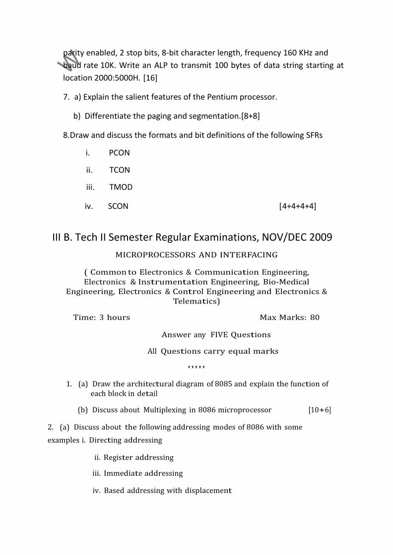
parity enabled, 2 stop bits, 8-bit character length, frequency 160 KHz and
baud rate 10K. Write an ALP to transmit 100 bytes of data string starting at
location 2000:5000H. [16]
7. a) Explain the salient features of the Pentium processor.
b) Differentiate the paging and segmentation.[8+8]
8.Draw and discuss the formats and bit definitions of the following SFRs
i. PCON
ii. TCON
iii. TMOD
iv. SCON [4+4+4+4]
III B. Tech II Semester Regular Examinations, NOV/DEC 2009
MICROPROCESSORS AND INTERFACING
( Common to Electronics & Communication Engineering, Electronics & Instrumentation Engineering, Bio-Medical
Engineering, Electronics & Control Engineering and Electronics & Telematics)
Time: 3 hours Max Marks: 80
Answer any FIVE Questions
All Questions carry equal marks
⋆ ⋆ ⋆ ⋆ ⋆
1. (a) Draw the architectural diagram of 8085 and explain the function of each block in detail
(b) Discuss about Multiplexing in 8086 microprocessor [10+6]
2. (a) Discuss about the following addressing modes of 8086 with some
examples i. Directing addressing
ii. Register addressing
iii. Immediate addressing
iv. Based addressing with displacement
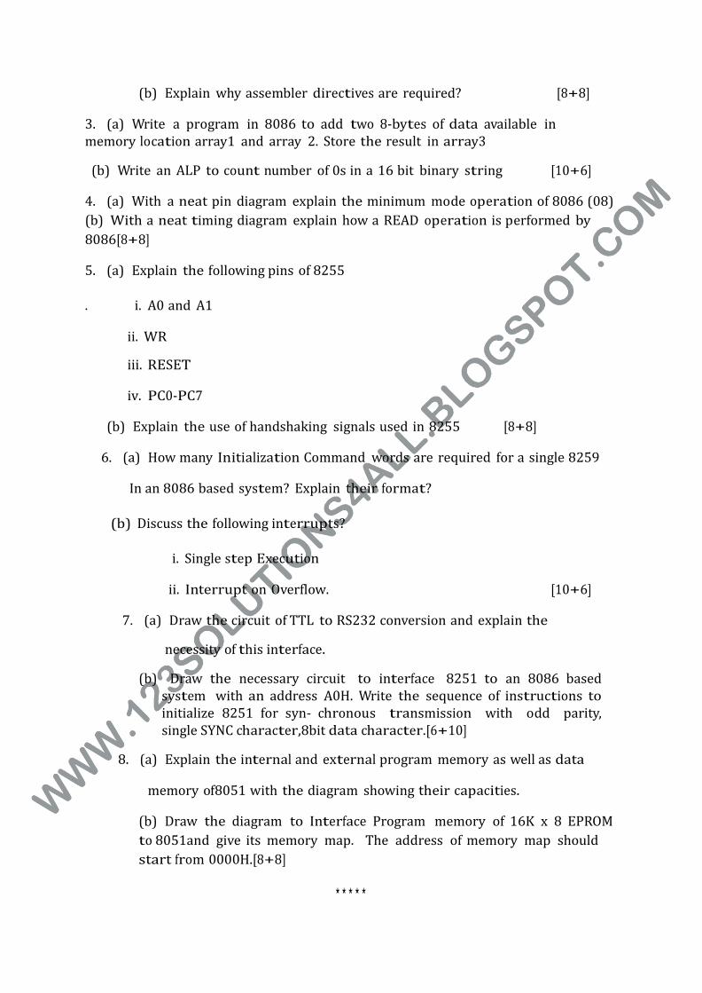
(b) Explain why assembler directives are required? [8+8]
3. (a) Write a program in 8086 to add two 8-bytes of data available in memory location array1 and array 2. Store the result in array3
(b) Write an ALP to count number of 0s in a 16 bit binary string [10+6]
4. (a) With a neat pin diagram explain the minimum mode operation of 8086 (08)
(b) With a neat timing diagram explain how a READ operation is performed by
8086[8+8]
5. (a) Explain the following pins of 8255
. i. A0 and A1
ii. WR
iii. RESET
iv. PC0-PC7
(b) Explain the use of handshaking signals used in 8255 [8+8]
6. (a) How many Initialization Command words are required for a single 8259
In an 8086 based system? Explain their format?
(b) Discuss the following interrupts?
i. Single step Execution
ii. Interrupt on Overflow. [10+6]
7. (a) Draw the circuit of TTL to RS232 conversion and explain the
necessity of this interface.
(b) Draw the necessary circuit to interface 8251 to an 8086 based system with an address A0H. Write the sequence of instructions to initialize 8251 for syn- chronous transmission with odd parity, single SYNC character,8bit data character.[6+10]
8. (a) Explain the internal and external program memory as well as data
memory of8051 with the diagram showing their capacities.
(b) Draw the diagram to Interface Program memory of 16K x 8 EPROM
to 8051and give its memory map. The address of memory map should
start from 0000H.[8+8]
⋆ ⋆ ⋆ ⋆ ⋆
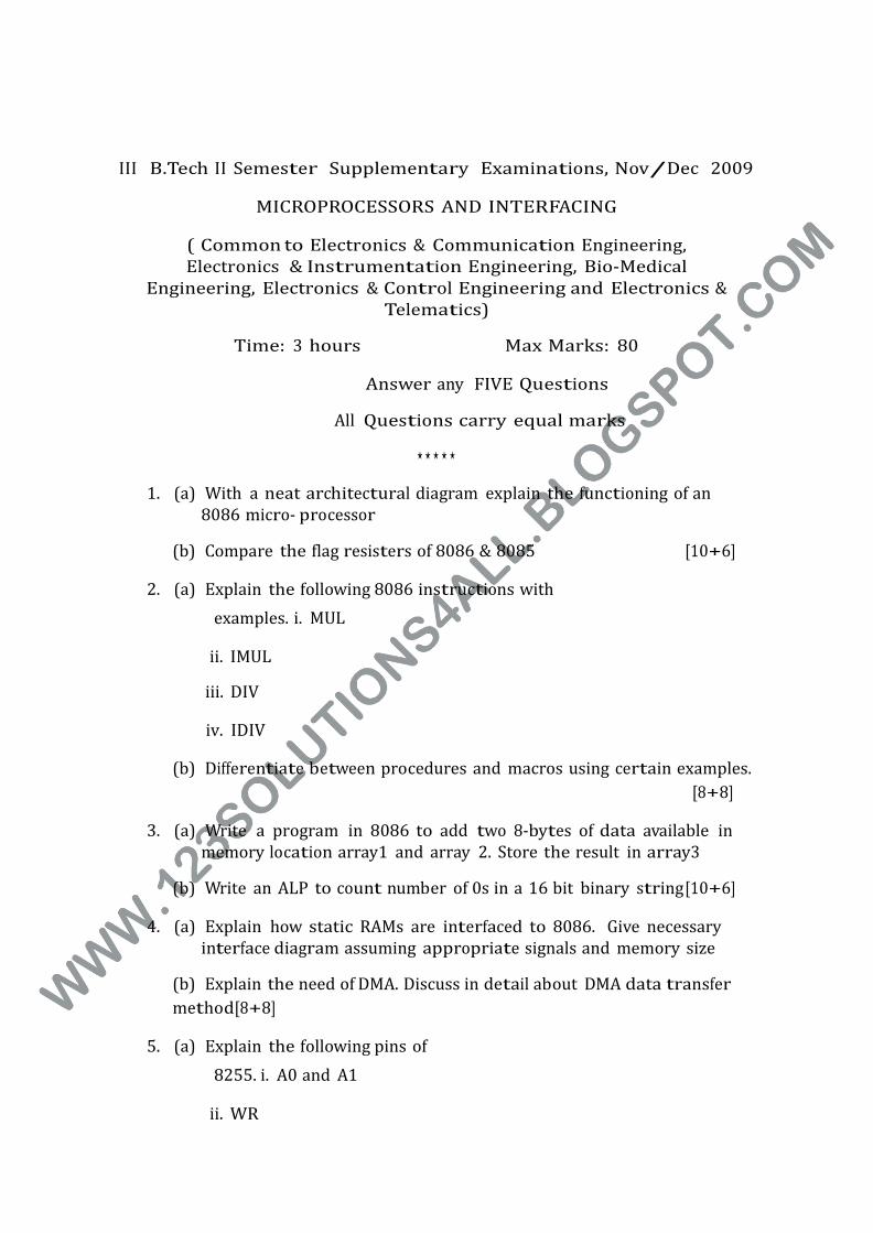
III B.Tech II Semester Supplementary Examinations, Nov/Dec 2009
MICROPROCESSORS AND INTERFACING
( Common to Electronics & Communication Engineering, Electronics & Instrumentation Engineering, Bio-Medical
Engineering, Electronics & Control Engineering and Electronics & Telematics)
Time: 3 hours Max Marks: 80
Answer any FIVE Questions
All Questions carry equal marks
⋆ ⋆ ⋆ ⋆ ⋆
1. (a) With a neat architectural diagram explain the functioning of an 8086 micro- processor
(b) Compare the flag resisters of 8086 & 8085 [10+6]
2. (a) Explain the following 8086 instructions with
examples. i. MUL
ii. IMUL
iii. DIV
iv. IDIV
(b) Differentiate between procedures and macros using certain examples.
[8+8]
3. (a) Write a program in 8086 to add two 8-bytes of data available in memory location array1 and array 2. Store the result in array3
(b) Write an ALP to count number of 0s in a 16 bit binary string [10+6]
4. (a) Explain how static RAMs are interfaced to 8086. Give necessary interface diagram assuming appropriate signals and memory size
(b) Explain the need of DMA. Discuss in detail about DMA data transfer
method[8+8]
5. (a) Explain the following pins of
8255. i. A0 and A1
ii. WR
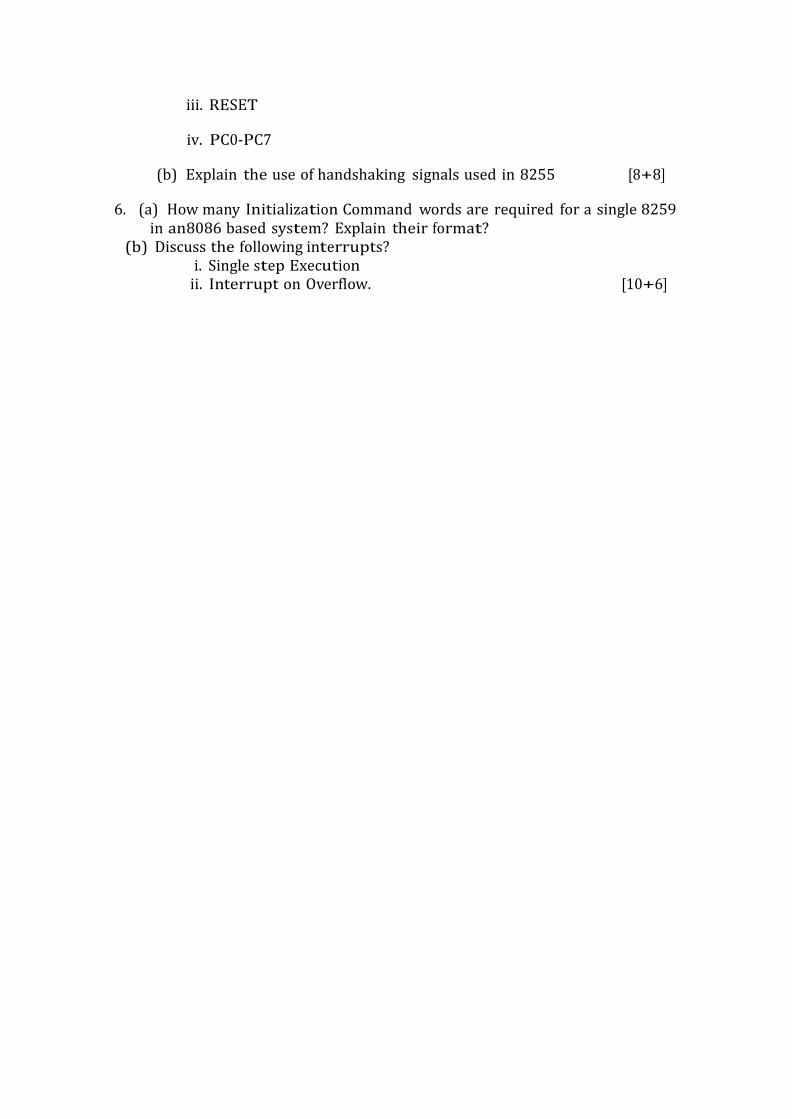
iii. RESET
iv. PC0-PC7
(b) Explain the use of handshaking signals used in 8255 [8+8]
6. (a) How many Initialization Command words are required for a single 8259 in an8086 based system? Explain their format? (b) Discuss the following interrupts?
i. Single step Execution ii. Interrupt on Overflow. [10+6]
1 of 1
7. (a) Explain why serial data transfer is mostly preferred over parallel data transfer.Give reasons. (b) Distinguish between data formats used for Synchronous and Asynchronous serial data transfer modes. [8+8]
8. (a) Draw and discuss the formats and bit definitions of the following registers of 8051.
i. IP ii. IE
(b) The internal RAM memory (128 bytes) is divided into three parts. Explain it with neat diagram? [8+8]
⋆ ⋆ ⋆ ⋆
III B.Tech II Semester Supplementary Examinations, Nov/Dec 2009
MICROPROCESSORS AND INTERFACING
( Common to Electronics & Communication Engineering, Electronics & Instrumentation Engineering, Bio-Medical
Engineering, Electronics & Control Engineering and Electronics & Telematics)
Time: 3 hours Max Marks: 80
Answer any FIVE Questions
All Questions carry equal marks
⋆ ⋆ ⋆ ⋆ ⋆
1. (a) Draw the architectural diagram of 8085 and explain the function of each block in detail
(b) Discuss about Multiplexing in 8086 microprocessor [10+6]
2. (a) Discuss about the following addressing modes of 8086 with some
examples i. Directing addressing
ii. Register addressing
iii. Immediate addressing
iv. Based addressing with displacement
(b) Explain why assembler directives are required? [8+8]
3. (a) Write an ALP in 8086 to sort a given set of 8-bit unsigned integers into as- cending order by bubble sort method
(b) Write an ALP in 8086 to display the string “WELCOME” on the screen
[10+6]
1 of 1
4. (a) With relevant pin diagrams explain the minimum and maximum mode oper- ations of 8086
(b) Explain briefly about DMA data transfer method. [12+4]
5. (a) Explain the modes of operation of 8255 with relevant diagrams?
(b) With a neat diagram explain how a 7-segment display is interfaced to 8086 using 8255? [8+8]
6. (a) Differentiate between Initialization Command Words and Operation Com- mand Words of 8259.
(b) Discuss about the interrupt priority schemes used in 8259. [10+6]
7. (a) Draw the circuit of RS232 to TTL conversion and explain this
interface?
(b) Draw the internal block diagram of 8251 USART and explain in detail about each block. [6+10]
8. (a) Explain the alternate functions of Port 0, Port 2 and Port 3.
(b) Draw and discuss the formats and bit definitions of TCON register in 8051. [8+8]
⋆ ⋆ ⋆ ⋆ ⋆
III B.Tech II Semester Supplementary Examinations, Nov/Dec 2009
MICROPROCESSORS AND INTERFACING
( Common to Electronics & Communication Engineering, Electronics & Instrumentation Engineering, Bio-Medical
Engineering, Electronics & Control Engineering and Electronics & Telematics)
Time: 3 hours Max Marks: 80
Answer any FIVE Questions
All Questions carry equal marks
⋆ ⋆ ⋆ ⋆ ⋆
1. Explain the function of following registers in 8086 microprocessor :
[4×4=16] (a)
AX,BX,CX,DX
(b) CS,DS,SS,ES

1 of 1
(c) BP,SP,SI,DI
(d) IP and Instruction Queue
2. (a) Discuss about the following addressing modes of 8086 with some
examples i. Directing addressing
ii. Register addressing
iii. Immediate addressing
iv. Based addressing with displacement
(b) Explain why assembler directives are required? [8+8]
3. (a) Write a program in 8086 to add two 8-bytes of data available in memory location array1 and array 2. Store the result in array3
(b) Write an ALP to count number of 0s in a 16 bit binary string [10+6]
4. (a) With relevant pin diagrams explain the minimum and maximum mode oper- ations of 8086
(b) Explain briefly about DMA data transfer method. [12+4]
5. (a) Write an ALP in 8086 to generate triangular waveform and give the necessary circuit setup with a DAC.
(b) Write an algorithm for driving a stepper motor. Assume that the desired direction stored in BL and the number of steps is stored in CL. Write a delay routine for 1 millisecond after each step movement. [8+8]
6. (a) How many Initialization Command words are required for a single 8259
in an
8086 based system? Explain their
format? (b) Discuss the following
interrupts?
i. Single step Execution
ii. Interrupt on Overflow. [10+6]
7. (a) Explain with a neat diagram the working of 8251
PCI. (b) Draw the interface circuits for data conversion
from
1 of 1
i. TTL to RS232C and
ii. RS232C to TTL [8+8]
8. (a) Discuss about various addressing modes of 8051.
(b) Explain the interrput structure of 8051 [8+8]
III B.Tech I Semester Examinations, November 2010
MICROPROCESSORS AND INTERFACING
Common to Information Technology, Instrumentation And Control Engineering, Electronics And Computer Engineering,
Computer Science And Engineering
Time: 3 hours Max Marks: 80
Answer any FIVE Questions
All Questions carry equal marks
1. (a) Explain the Interrupts of 80286 in the order of priority?
(b) Explain the salient features of Pentium Processor? [8+8]
2. (a) Explain memory addressing modes of 8086? Give an example for each ad- dressing mode?
(b) What is the purpose of Trap flag? Discuss how debugging feature is provided with the help of Trap flag in 8086? [8+8]
3. Describe the function of the following pins in 8086 maximum mode of
operation. (a) MN/ M X
(b) RQ/GT0 and RQ/GT1
(c) QS0 & QS1
(d) LOC K [16]
4. (a) Using REPEAT-UNTIL construct, develop a sequence of 8086 instructions that reads a character string from the keyboard and
1 of 1
after pressing the enter key the character string is to be displayed again.
(b) What is a procedure? Give an example to declare a procedure as near? Make this procedure as PUBLIC procedure? [8+8]
5. (a) Explain the application of stepper motor in microcomputers?
(b) Explain with a neat block diagram the working of dual slope ADC? How do you interface the dual slope ADC to microprocessor? Give the required instruction sequence to acquire one sample from ADC? [8+8]
6. (a) Discuss the following signal descriptions?
i. I N T0/I N T1
ii. TXD
iii. T0 AND T1
iv. RD
(b) Draw and discuss the formats and bit definitions of the following SFRs in 8051 microcontroller?
i. TMOD
ii. PSW [8+8]
7. In an 8086 based system it is necessary to serve 64 IRQs from different
initiators.The allocated address space for 8259s is from 0700h to 070FH.
Give the complete design by choosing the appropriate address locations
in the above range? Give the initialization sequence for all 8259’s with
each IRQ activated in level triggered mode and the starting interrupt is
type 40H? [16]
8. (a) What are the MODEM control lines? Explain the function of
each line?
Discuss how MODEM is controlled using these lines with necessary sequence of instructions?
(b) Interface 8251 with 8086 at address 0F0H. Initialize it in asynchronous mode, with 8 bit character size, baud rate factor 16, one start bit, two stop bits, even parity enable? [8+8]
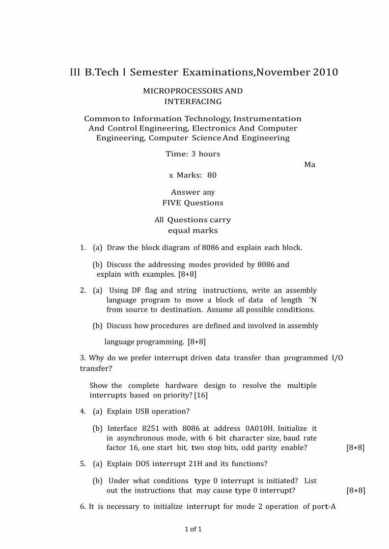
1 of 1
III B.Tech I Semester Examinations,November 2010
MICROPROCESSORS AND
INTERFACING
Common to Information Technology, Instrumentation And Control Engineering, Electronics And Computer
Engineering, Computer Science And Engineering
Time: 3 hours
Ma
x Marks: 80
Answer any
FIVE Questions
All Questions carry
equal marks
1. (a) Draw the block diagram of 8086 and explain each block.
(b) Discuss the addressing modes provided by 8086 and explain with examples. [8+8]
2. (a) Using DF flag and string instructions, write an assembly language program to move a block of data of length ‘N from source to destination. Assume all possible conditions.
(b) Discuss how procedures are defined and involved in assembly
language programming. [8+8]
3. Why do we prefer interrupt driven data transfer than programmed I/O
transfer?
Show the complete hardware design to resolve the multiple interrupts based on priority? [16]
4. (a) Explain USB operation?
(b) Interface 8251 with 8086 at address 0A010H. Initialize it in asynchronous mode, with 6 bit character size, baud rate factor 16, one start bit, two stop bits, odd parity enable? [8+8]
5. (a) Explain DOS interrupt 21H and its functions?
(b) Under what conditions type 0 interrupt is initiated? List out the instructions that may cause type 0 interrupt? [8+8]
6. It is necessary to initialize interrupt for mode 2 operation of port-A
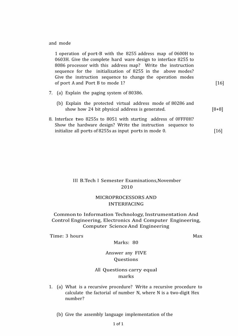
1 of 1
and mode
1 operation of port-B with the 8255 address map of 0600H to 0603H. Give the complete hard ware design to interface 8255 to 8086 processor with this address map? Write the instruction sequence for the initialization of 8255 in the above modes? Give the instruction sequence to change the operation modes of port A and Port B to mode 1? [16]
7. (a) Explain the paging system of 80386.
(b) Explain the protected virtual address mode of 80286 and show how 24 bit physical address is generated. [8+8]
8. Interface two 8255s to 8051 with starting address of 0FFF0H? Show the hardware design? Write the instruction sequence to initialize all ports of 8255s as input ports in mode 0. [16]
III B.Tech I Semester Examinations,November
2010
MICROPROCESSORS AND
INTERFACING
Common to Information Technology, Instrumentation And Control Engineering, Electronics And Computer Engineering,
Computer Science And Engineering
Time: 3 hours Max
Marks: 80
Answer any FIVE
Questions
All Questions carry equal
marks
1. (a) What is a recursive procedure? Write a recursive procedure to calculate the factorial of number N, where N is a two-digit Hex number?
(b) Give the assembly language implementation of the
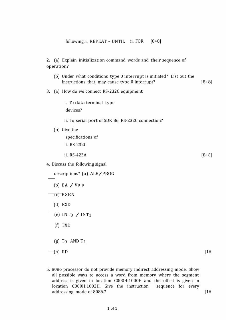
1 of 1
following. i. REPEAT – UNTIL ii. FOR [8+8]
2. (a) Explain initialization command words and their sequence of
operation?
(b) Under what conditions type 0 interrupt is initiated? List out the instructions that may cause type 0 interrupt? [8+8]
3. (a) How do we connect RS-232C equipment
i. To data terminal type
devices?
ii. To serial port of SDK 86, RS-232C connection?
(b) Give the
specifications of
i. RS-232C
ii. RS-423A [8+8]
4. Discuss the following signal
descriptions? (a) ALE/PROG
(b) EA / VP P
(c) P SEN
(d) RXD
(e) I N T0 / I N T1
(f ) TXD
(g) T0 AND T1
(h) RD [16]
5. 8086 processor do not provide memory indirect addressing mode. Show all possible ways to access a word from memory where the segment address is given in location C000H:1000H and the offset is given in location C000H:1002H. Give the instruction sequence for every addressing mode of 8086.? [16]
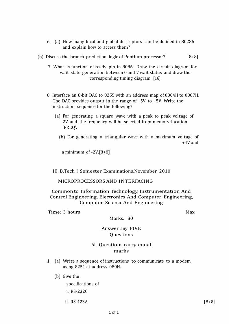
1 of 1
6. (a) How many local and global descriptors can be defined in 80286 and explain how to access them?
(b) Discuss the branch prediction logic of Pentium processor? [8+8]
7. What is function of ready pin in 8086. Draw the circuit diagram for wait state generation between 0 and 7 wait status and draw the
corresponding timing diagram. [16]
8. Interface an 8-bit DAC to 8255 with an address map of 0804H to 0807H. The DAC provides output in the range of +5V to - 5V. Write the instruction sequence for the following?
(a) For generating a square wave with a peak to peak voltage of 2V and the frequency will be selected from memory location ’FREQ’.
(b) For generating a triangular wave with a maximum voltage of +4V and
a minimum of -2V.[8+8]
III B.Tech I Semester Examinations,November 2010
MICROPROCESSORS AND INTERFACING
Common to Information Technology, Instrumentation And Control Engineering, Electronics And Computer Engineering,
Computer Science And Engineering
Time: 3 hours Max
Marks: 80
Answer any FIVE
Questions
All Questions carry equal
marks
1. (a) Write a sequence of instructions to communicate to a modem using 8251 at address 080H.
(b) Give the
specifications of
i. RS-232C
ii. RS-423A [8+8]
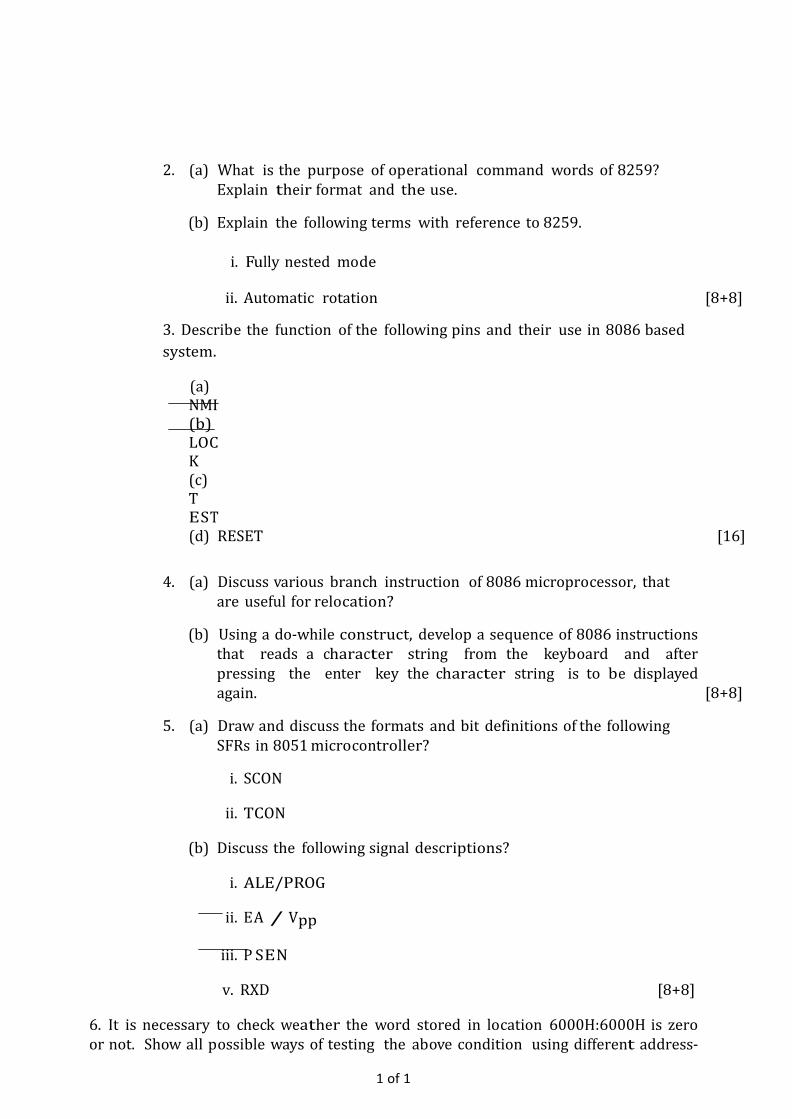
1 of 1
2. (a) What is the purpose of operational command words of 8259? Explain their format and the use.
(b) Explain the following terms with reference to 8259.
i. Fully nested mode
ii. Automatic rotation [8+8]
3. Describe the function of the following pins and their use in 8086 based
system.
(a) NMI (b) LOC K (c) T EST (d) RESET [16]
4. (a) Discuss various branch instruction of 8086 microprocessor, that are useful for relocation?
(b) Using a do-while construct, develop a sequence of 8086 instructions that reads a character string from the keyboard and after pressing the enter key the character string is to be displayed again. [8+8]
5. (a) Draw and discuss the formats and bit definitions of the following SFRs in 8051 microcontroller?
i. SCON
ii. TCON
(b) Discuss the following signal descriptions?
i. ALE/PROG
ii. EA / Vpp
iii. P SEN
v. RXD [8+8]
6. It is necessary to check weather the word stored in location 6000H:6000H is zero or not. Show all possible ways of testing the above condition using different address-
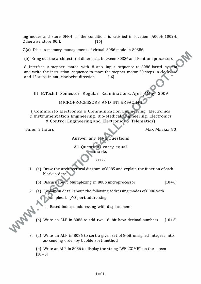
1 of 1
ing modes and store 0FFH if the condition is satisfied in location A000H:1002H. Otherwise store 00H. [16]
7.(a) Discuss memory management of virtual 8086 mode in 80386.
(b) Bring out the architectural differences between 80386 and Pentium processors.
8. Interface a stepper motor with 8-step input sequence to 8086 based system and write the instruction sequence to move the stepper motor 20 steps in clockwise and 12 steps in anti-clockwise direction. [16]
III B.Tech II Semester Regular Examinations, April/May 2009
MICROPROCESSORS AND INTERFACING
( Common to Electronics & Communication Engineering, Electronics & Instrumentation Engineering, Bio-Medical Engineering, Electronics
& Control Engineering and Electronics & Telematics)
Time: 3 hours Max Marks: 80
Answer any FIVE Questions
All Questions carry equal marks
⋆ ⋆ ⋆ ⋆ ⋆
1. (a) Draw the architectural diagram of 8085 and explain the function of each block in detail
(b) Discuss about Multiplexing in 8086 microprocessor [10+6]
2. (a) Explain in detail about the following addressing modes of 8086 with
examples. i. I/O port addressing
ii. Based indexed addressing with displacement
(b) Write an ALP in 8086 to add two 16- bit hexa decimal numbers [10+6]
3. (a) Write an ALP in 8086 to sort a given set of 8-bit unsigned integers into as- cending order by bubble sort method
(b) Write an ALP in 8086 to display the string “WELCOME” on the screen
[10+6]
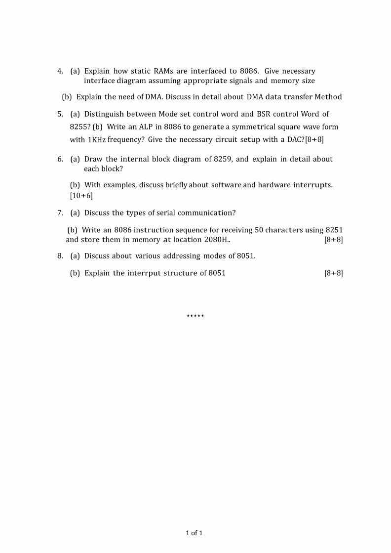
1 of 1
4. (a) Explain how static RAMs are interfaced to 8086. Give necessary interface diagram assuming appropriate signals and memory size
(b) Explain the need of DMA. Discuss in detail about DMA data transfer Method
5. (a) Distinguish between Mode set control word and BSR control Word of
8255? (b) Write an ALP in 8086 to generate a symmetrical square wave form
with 1KHz frequency? Give the necessary circuit setup with a DAC? [8+8]
6. (a) Draw the internal block diagram of 8259, and explain in detail about each block?
(b) With examples, discuss briefly about software and hardware interrupts.
[10+6]
7. (a) Discuss the types of serial communication?
(b) Write an 8086 instruction sequence for receiving 50 characters using 8251 and store them in memory at location 2080H.. [8+8]
8. (a) Discuss about various addressing modes of 8051.
(b) Explain the interrput structure of 8051 [8+8]
⋆ ⋆ ⋆ ⋆ ⋆
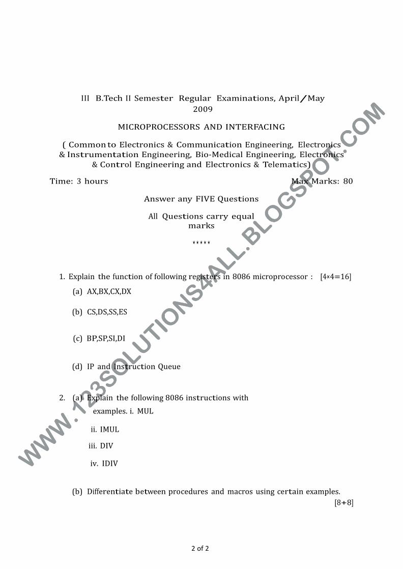
2 of 2
III B.Tech II Semester Regular Examinations, April/May
2009
MICROPROCESSORS AND INTERFACING
( Common to Electronics & Communication Engineering, Electronics & Instrumentation Engineering, Bio-Medical Engineering, Electronics
& Control Engineering and Electronics & Telematics)
Time: 3 hours Max Marks: 80
Answer any FIVE Questions
All Questions carry equal marks
⋆ ⋆ ⋆ ⋆ ⋆
1. Explain the function of following registers in 8086 microprocessor : [4×4=16]
(a) AX,BX,CX,DX
(b) CS,DS,SS,ES
(c) BP,SP,SI,DI
(d) IP and Instruction Queue
2. (a) Explain the following 8086 instructions with
examples. i. MUL
ii. IMUL
iii. DIV
iv. IDIV
(b) Differentiate between procedures and macros using certain examples.
[8+8]
2 of 2
3. (a) Write a program in 8086 to add two 8-bytes of data available in memory location array1 and array 2. Store the result in array3
(b) Write an ALP to count number of 0s in a 16 bit binary string [10+6]
4. (a) With a neat block diagram, explain the working of 8257 DMA
controller
(b) Explain briefly about memory interfacing with 8086 microprocessor
[10+6]
5. (a) Write an ALP in 8086 to generate triangular waveform and give the necessary circuit setup with a DAC.
(b) Write an algorithm for driving a stepper motor. Assume that the desired direction stored in BL and the number of steps is stored in CL. Write a delay routine for 1 millisecond after each step movement. [8+8]
6. (a) Distinguish between interrupts and exceptional handling interrupts
(b) Discuss about the following terms:
i. Vector interrupt table and lookup table.
ii. Interrupt service routines and subroutines. [8+8]
7. (a) Discuss the types of serial communication?
(b) Write an 8086 instruction sequence for receiving 50 characters using 8251 and store them in memory at location 2080H.. [8+8]
8. (a) Explain the internal and external program memory as well as data
memory of 8051 with the diagram showing their capacities.
(b) Draw the diagram to Interface Program memory of 16K x 8 EPROM to
8051and give its memory map. The address of memory map should start from 0000H. [8+8]
⋆ ⋆ ⋆ ⋆ ⋆
III B.Tech II Semester Regular Examinations, April/May 2009
MICROPROCESSORS AND INTERFACING
( Common to Electronics & Communication Engineering, Electronics & Instrumentation Engineering, Bio-Medical Engineering, Electronics &
Control Engineering and Electronics & Telematics)
Time: 3 hours Max Marks: 80
Answer any FIVE Questions
All Questions carry equal marks
⋆ ⋆ ⋆ ⋆ ⋆
1. (a) Compare the Interrupt structure of 8086 and 8085 Microprocessors. Also discuss about priorities of the interrupts in both the cases.
(b) With examples ,explain how multiplexing is implemented in 8086 Microproces- sor [10+6]
2. (a) Explain in detail about the following addressing modes of 8086 with
examples. i. I/O port addressing
ii. Based indexed addressing with displacement
(b) Write an ALP in 8086 to add two 16- bit hexa decimal numbers [10+6]
3. (a) Write an ALP in 8086 to count number of positive and negative numbers from an array of 8-bit integers
(b) Write an ALP in 8086 to exchange a block of N bytes of data between source and destination [8+8]
4. (a) With relevant pin diagrams explain the minimum and maximum mode oper- ations of 8086
(b) Explain briefly about DMA data transfer method. [12+4]
5. (a) With a neat internal architectural diagram, explain the features of
8255?
(b) Explain the interfacing of a stepper motor with 8086 using the ports of 8255? [8+8]
6. (a) What is the purpose of operational command words of 8259? Explain their format and the use?
(b) Discuss the following
interrupts. i. Divide Error
ii. Non Maskable interrupt
iii. Break Point interrupt [10+6]
7. (a) Write the instruction sequence in 8086 to initialize the 8251
(b) Draw and explain the block diagram of 8251. [8+8]
8. (a) Draw the architectural diagram of 8051 microcontroller and explain in detail about each block.
(b) Explain the basic differences between a microprocessor and a microcontroller.
[10+6]
17.Question bank:
UNIT-1
General definitions of mini computers etc,.
1. What are the advantages and the limitations microcontroller over a Microprocessor?
2. Describe the main blocks in a digital signal processor that are not in a general
Microprocessor?
3. Overview of 8085 Microprocessor
4. List the internal registers in 8085 microprocessor and their abbreviations and
lengths. Describe the primary function of each register.
5. Differentiate between NMI and MI interrupts
6. Explain how with external hardware TRAP can be masked
7. Explain the timing diagrams of 8085 when it is executing Memory mapped I/O
and I/O mapped I/O instructions
B) Explain the following pins of 8085 microprocessor
i) SID,SOD ii) ALE iii) HOLD,HLD iv) TRAP
8.Explain the features of 8086
9. Explain architecture if 8086
10. Explain the function of following registers in 8086 microprocessor.
a) AX, BX, CX, DX. b) CS, DS, SS, ES. C) BP, SP, SI ,DI.
d) IP & instruction queue e) Flags.
UNIT-2
1. List out the addressing modes of 8085, & Explain each with an example
2. Write a algorithm & ALP to reverse the bits in a 16-bit number & check weather it is a
Palindrome or not.
3.Explain all branch and call instructions
4. Write an ALP for Ascending and Descending of a series
5.Write an ALP for Matrix multiplication
6. Explain the meaning of the following 8086 instructions.
i) MOV [3845H],BX ii) ADD AX,[SI]
iii) MOV BX,2956H iv) ADC AX,BX.
7. Explain string instructions supported by 8086 processor.
8. Write a algorithm & ALP to reverse the bits in a 16-bit number & check weather it is a
Palindrome or not.
9. If BH = 0F3H what is the value of BH in hex after the instruction SAR BH, 1
10. IF AL = 78H and BL=73H explain how DAS instruction ( after subtracting BL
From AL ) adjusts to the BCD result
11. If CL=78H what is the value of CL after the instruction ROL CL, 3
12. Why AAD is to be executed before DIV instruction while converting unpacked
BCD to Binary number
13. Under what conditions REPE MOVS executes
14. Explain XLAT instruction to linearize transducer characteristics
15. Explain intra segment and inter segment branch instructions with examples the
instructions related to arithmetic and logical shift.
16. Explain all addressing modes with the assembler syntax and how effective
address is calculated
UNIT-3
1.How do you configure 8086 into minimum and maximum modes
2.Bring out the differences between 8086 and 8088 processors
3.Explain all the features in 8284
4.Why and when wait states are required. How do you insert wait states1.
5. . In an SDK-86 kit 128KB SRAM & 64KB EPROM is provided on system and provision
Expansion of another 128KB SRAM is given. Then on system SRAM address starts from
00000H & EPROM ends with FFFFFH. The expansion slot address map is from 80000H
To 9FFFFH. The size of SRAM chip is 64KB, EPROM chip size is 16KB.Give the
Complete memory interface and also the address map for complete memory map for
Individual chips..
6. What are the steps in interfacing peripherals with the micro processor?
7. Sketch and explain the interface of PPI 8255 to the 8086 microprocessor in
minimum mode. Interface 4 7 segment LEDs to display as a BCD counter
8. In the above question Q2 interface two keys UP and DOWN to the PPI. Write an
8086 assembly program segment such that when UP is pressed the counter counts
up every second. Similarly when DOWN key is pressed the counter decrements
every second
9. Sketch and explain the interface of 8279 to the 8086 microprocessor in minimum
mode. Interface 8x8 key pad and 16x 7 Seg LED display. Write an 8086 assembly
program to read the key codes of keys and display -NPTEL-INDIA
10. Sketch and explain the interface of PIT 8254 to the 8086 microprocessor in
minimum mode. Cascade two counters in the PIT. Write a program segment two
get one minute delay
11What are the differences in interfacing RWMs while 8086 is in minimum and
maximum modes?
12. Sketch and explain the interface of 32K x 16 RWMs using a decoder in minimum
mode. What is the maximum access time of ROMs such that it does not require
wait states when 8086 operates at 8 MHz?
13. Sketch and explain the timing diagrams in the above interface Question 2
14 Sketch and explain the 8086 bus activities during write machine cycle
15.Review on Interrupt Structure of 8086
16.Explain serial data transfer schemes
17.Pin configuration of 8251
18.Architectural features of 8251
19.Sending and receiving a character
UNIT-4
1. What are the advantages and disadvantages of using Harvard architecture in
8051?
2. How much maximum external program memory can be interfaced?
3. Explain PSW SFR. Give the application differences between Carry and Overflow
flags
4. What are the power consumptions in power down and idle modes
5. Explain Quasi Bidirectional ports of 8051
6. What is the status of all registers on reset?
7. What is the maximum delay the Timer0 produces when 8051 is operated at
12MHz?
8. Explain how in Serial communication mode 0 expands I/O lines with the help of
Shift
UNIT-5
1.explain timers/counters?
2.explain different modes of timers/counters?
3.explain serial communication concepts in 8051?
4.explain different modes in serial communication?
5.explain interrupt structure of 8051?
18.Assignment Questions
UNIT 1
1. Explain pin description of 8086 with functional pin daiagram.
2. Draw the 8086 architecture diagram and explain various blocks of the diagram. Detail
the Register organization in 8086.
3. What is memory segmentation? Describe physical memory organization. How to
calculate the physical memory address.
4. Describe minimum mode and maximum mode operation in 8086 along with Timing
diagrams.
5. Explain programmers model and flag register format of 8086
UNIT 2
1. Explain the instruction formats in 8086. give the complete instruction set of 8086 along
with examples.
2. What is an addressing mode? Explain various addressing modes of 8086 along with
examples.
3. What is an assembler directive and Macro? Give the differences between Procedure and
Macro.Explain Assembler directives, Procedures and Macros with the help of examples.
4. Write ALP for
a. to perform multi-byte addition.
b. to perform the sorting N numbers.
c. to display the string "GEETHANJALI"
d. to move a block of data from source to destination.
e. to evaluate the expression s = uv + v²
UNIT 3
1. Explain 8255 architecture and various modes of data transfer.
2. Keyboard and display interfacing
3. ADC and DAC interfacing
4. Stepper motor interfacing
5. Explain how memory is interfaced with 8086. Write memory connection diagrams for
minimum mode and maximum mode operation of 8086.
6. Explain interrupt structure of 8086. What is vector table? what are the operations done during
handling an interrupt service routine?
7. Explain why serial data transfer is mostly preferred over parallel data transfer.
Give reasons? Discuss the types of serial communication?
8. Draw the internal block diagram of 8251 USART and explain in detail about each
block.
9. With a neat circuit diagram, explain the interfacing of 8251 with 8086
10. Design a hardware interfacing circuit for interfacing 8251 with 8086. Set the 8251A in
asynchronous mode as a transmitter and receiver with even parity enabled, 2 stop bits, 8-
bit character length, frequency 160 KHz and baud rate 10K. Write an ALP to transmit 100
bytes of data string starting at location 2000:5000H.
11. Give the description about the following.
RS-232 standard
Ttl to rs232 conversion
Rs232 to ttl conversion.
UNIT-4
1.8051 microcontroller architecture
2. Register organization of 8051
3. Addressing modes and i/o ports of 8051.
4. Memory organisation of 8051.
5. Operation of I/O ports.
UNIT-5
1. programming Timer/counter and Various modes of operation of timers.
2. Serial communication operation
3. Memory interfacing
4. Programming external hardware interrupts
19. Unit-wise quiz questions
-----------------flag is used in 8086 for string manipulation instructions
A DF
B AF
C OF
D
8086 as -------------------- of segment registers
A 3
B 5
C 4
D 2
A ..……….. is an identifier that is assigned the address of the first byte of the instruction in
which it appears
A Operand
B mnemonic
Label
D Comment
In which instruction the flags are not affected
A LDS
B DAA
C ADC
D DAS
Data storage in stack is designed in _______________method.
First in first
out
B last in last out
first in last out
last in first out
--------------- instruction is used to call a procedure
A CALL
B RET
C PROC
D NEAR
--------------is a prefix used in 8086 machine language that simplifies the use of string primitives
with loops
REP
B LOOP

C LODS
D MOVS
LODSB instruction will automatically increment __________register.
A DI
B SI
C DS
D ES
----------- is a special component used in 8086 for block transfer of data to or from a port
A BMA
B DNA
C
The first operand in the IN instruction must be ----------register for byte transfer
A CL
B BL
AL
D DL
In ______________ environment two or more process is executed in a time multiplexed
fashion
A Uniprogramming
B Multiprogramming
C I/O operation
D DMA
Preventing two or more process from simultaneously entering their critical sections for
accessing a shared resource is called-----------------------
A Mutual sharing
B Mutual process
Mutual exclusion
D mutual accessing
…………….IC is used as clock generator for 8086
A 8087
B 8284
C 8088
D 8294
A processor is in minimum mode when its MN/MX pin is strapped to -------volts
A +50
B +5
C 0
D -5
8086 is interfaced with -------------Co-processor to perform float point calculations.
A 8089
B 8085
C 8087
D 8084
An instruction to be executed by the coprocessor is indicted when ----------instruction
appears in the program sequence
A TRUE
B FALSE
C TEST
D ESC
One of the following addressing modes is not possible in 8085.
A Indexed addressing
B Indirect addressing
C Direct addressing
D Indirect register address
The speed of a microprocessor is usually measured by the
A Microprocessor‘s throughput.
B Speed with which it performs I/P and O/P operations.
C Time required executing a basic instruction.
D Time required processing a small operation
Which of the following is an 8085 hardware interrupt?
A TRAP,
B RST6.5
C RST7.5,
D All the above
Which of the following is does NOT belong to 8085 flag register
A Carry flag
B Sign flag
C Zero flag
D One flag
DAD re instruction mean
A Add the content of specified reg. to center of HL & store the result in HL
B Add 8 bit data given in inst‖ to center of one & store the result in reg
C Add 10 bit data given in inst to contact of HL & stout the result in HL
D
None of the above
Instruction that sets the carry flag
A CY set
B STR
C STC
D Set CY
Instruction that avoids unnecessary jumps to terminate the prog
A NOP
HLT
C ei
D O
Instruction cycle can be dined as sum of
A Instruction fetch + Instruction decode
B Instruction fetch + instruction Execute
C Instruction fetch + instruction exit
D All of abov
Instruction cycle use ________ m/c cycle,
A 1-5
B 1-16
C 1-8
D None of above
Each m/c cycles have ________ T states
A 3 to 6t
B 3 to 10t
C 3 to 8t
D None of above
Which of the following does the task of displaying the result computed by the microprocessor?
A Cathode Ray Tube (CRT)
B Light-Emitting diodes (LED‘S)
C Laser printer
D All of the above.
In 8086 microprocessor which of the following is Not a register pair register
A B-C pair
F-G pair
C H-L pair
D D-E pair
Zero Flag is to _____ if the result of an arithmetic operation is zero.
1
B 0
C -
1
D 2
Two‘s complement representation of -2 is ________
A 0010
B 0110
C 1110
D 0011
If there are two operands, the _______ operand appears first.
A destination
B Destination
C source
D labe
An interrupt initiated by a signal on the NMI pin is called a __________
A NON maskable interrupt
B Number mask able interrupt
C NOT mask able interrupt
D None of the abov
There are two power connection for +5 volts in 8085 they are
A Vss and Vgg
Vcc and Vss
C Vcc and Vgg
D None of the above
Which of the following is the function of microprocessor
A Receiving input
B Performing computations.
C Storing data & instructions
D All of the above.
---------------- and --------------- lines provide the 8085 with a DMA capability by allowing
another processor on the same system bus to request control of the buses
A S0,S1
B Read and Write
C ALE and READY
D HOLD and HLDA
----------------and ------------------- instructions provide a means of moving two bytes between HL
register and a RAM address
A LDAX & STAX
B LHLD & SHLD
C LDA& STA
D PUSH & POP
The binary representation of decimal number 34.56is …………………..
A 100011.100
B 100010.110

C 100010.100
D 100011.111
The octal representation of hexadecimal number CD is ……………………….
A 315
B 305
C 335
D 312
8086 processor has ------------- address pins out of which ---------------- number of pins are used
as data pins
A 16,8
B 16,14
C 20,16
D 20,8
In 8086 is a --------------------bit microprocessor and is fabricated using ------------technology
A 16,CMOS
B 8,HMOS
C 20,NMOS
D 16,HMOS
_________ and___________instructions are specifically used to change the status of carry flag
A STI,CLI
B STC,CLC
C MOV,LEA
D DAA,XCHG
In 8086 the …………instruction is used to simplify the decrementing, testing and branching.
This instruction uses _______as Counter register.
Loop, CX
B JMP, CX
C DEC, AX
D INC, AX
Two general class of interrupt are__________________ and _______________
A Pointer and vector
B IN and OUT
C input and output
D internal ,external
A ________is a segment of code that needs to be written only once but whose basic structure can
be caused to be repeated several times within a source module but placing a single statement at
the point of each appearance
A Micro
B Macro
C prototype
D interrupt
Packed BCD format of number 01 02 04 05 is ------------------and unpacked BCD format
of Number 5789 is-------------------
A 10203040, 50 70 80 09
B 11223344, 55 67 78 99
C 1234, 05 07 08 09
D 10203040,05 07 08 09
In 8086 __________instruction is specially designed for executing procedure .this instruction
assumes the base address of the byte array is in BX register and the byte to be converted is in the
________register
A ASCII, CX
B EBCDIC, CX
C PCHL, AL
D XLAT, AL
In 8086 all programmed communication with the I/O ports is done by the ----------- and -----------
- instructions
A MOV, OUT
B LOAD, MOVE
C IN, OUT
D IN, LOAD
In 8086 the external interrupts is caused by a signal sent to CPU through one of its pins they are
__________and ___________.
A NMI, IRET
B INTR, RET
C NMI, INTR
D RET,IRET
In _____________ memory management system fragmentation problem appear. Fragmentation
problem can be eliminated by------------------allocation scheme
A Partition allocation, relocation partition
B virtual memory, relocation partition
C dynamic ,partition
D relocation partition, dynamic
57.8086 can be operated in Two modes they are -----------------------and--------------
A Minimum, Maximum
B External, internal
C Mode1, Mode2
D Data, address
-------------------IC is designed specifically to work with 8086 as programmable interrupt
controller, it contains--------number of pins
A 8259,28
B 8269,28
C 8279,26
D 8299,26
The 8087 internally stores all numbers in the ------------- format which uses 15 bits for the
exponent and -------- bits for the manitissa
A permanent real,32
B temporary real,64
C permanent integer,32
D temporary integer,64
8087 numeric data processor is specially designed to perform arithmetic operations it can operate
on data with length ranging from --------- to --------------
A 2, 6
B 2, 10
C 4, 8
D 4, 10
Interrupt type is given a number between _____and___________ and the address of the interrupt
pointer is found by multiplying the type by ___________if type is 9 then the interrupt pointer
will be in bytes----------------through ----------------
A 0 and 256, 5, 00025 through 00030
B 0 and 200, 4, 00020 through 00024
C 0 and 200,4, 00024 through 00028
D 0 and 255,4,00024 through 00027
he 8086 receives bus request through its ………. pin and issues grants from its ………… pin .A
request is made when a potential master sends ……. to ………… pin
A HOLD,HLDA,1,HOLD
B HLDA,HOLD,1,HLDA
C HOLD,HLDA,0,HOLD
D HLDA,HOLD,0,HLDA
Intel IC 8286 transceiver device contains ---------- tristate elements, ------------receivers and ------
-------drivers. In order to operate 8086 in minimum mode -----------number of 8286ICs are
needed.
A 8,4,4,2
B 10,5,5,1
C 6,3,3,1
D 16,8,8,2
The binary representation of hexadecimal number ABC is
10101011110
0
101010111000
011010111100
101010111111
Subtracting octal number 478 from octal number 568 results in ………………….
5
7
6
8
8085 micro processor is an --------------- device
PMOS
CMOS
NMOS
QMOS
--------------- register deals with sequencing the execution of instructions
Stack pointer
program counter
accumulator
flag
1. Mode 1 of 8255 is used for which of these I/O methods
( a) Bi-Directional Handshake
( b ) DMA I/O
( c ) Strobed or Hand Shake mode
( d ) Simple Input/Output
2 . If the 8255 is selected for addresses 0F800H to 0F806H,
which one of the following is the address of PORT C
(a) 0F806H
( b ) 0F802H
( c ) 0F804H
( d ) 0F800H
3 . If 8 seven segment led multiplexed displays including the
decimal point are connected. How many wires are needed to
connect the segments (not including power supply wires)?
( a) 15
( b ) 16
( c ) 56
( d ) 64
4 . The diode kept across the coil of a step per motor is for ?
( a) Shorting the Back EMF
( b ) To stop the step per motor
( c ) Stopping flow of current
( d ) Allowing flow of current
5 . In the A/D converter ADC0808 which of these signals tri
states the digital output of ADC
( a) EOC
( b ) ALE
( c ) SOC
( d ) OE
6 . The fourth response of the 8086 to an interrupt is which
one of the following ?
( a) Decrements the SP by 2 & pushes flag register
( b ) It disables interrupt flag
( c ) Decrements the SP& pushes current CS contents
( d ) Resets Trap Flag
7 . What is the size of the vector interrupt table?
( a) 256 bytes
( b ) 65536 bytes
( c ) 1024 bytes
( d ) 4096 bytes
8 . Which of these values in AH perform input from keyboard ?
( a) 02 ( b ) 09 ( c ) 17 ( d ) 01
9 . Which one of these BIOS services is used for Mouse
Operation?
( a) 10H
( b ) 13H
( c ) 16H
( d ) 33H
10. The PIC interrupt controller which Masks the Interrupt is?
( a) IRR
( b ) IMR
( c ) ISR
( d ) PR
11. Data line which can be transfer in only one direction is
referred as
( a) Half Duplex
( b ) Com plex
( c ) Full Duplex
( d ) Simplex
12. In the Synchronous mode the 8251 which signal indicates
that the specified Synchronous character is received?
( a) Tx C
( b ) SYNDET/BD
( c ) CLK
( d ) C/D
13. The outer loop counter for N numbers is
( a) N-1 ( b ) N-2 ( c ) N ( d ) N/2
1 4. If the CPU has not read a character from the 8251 before
the arrival of the next character. Which of the following errors
is supposed to have occurred?
( a) Even Parity error
( b ) Framing Error
( c ) Over Run Error
( d ) Odd Parity Error
15. USB stands for which one of the following?
( a) Universal Sequential Bus
( b ) Universal Serial Bus
( c ) College Bus
( d ) Universal Sequential Bus
16. The 8051 is a
( a) 32 bit micro controller
( b ) 24 bit micro controller
( c ) 1 6 bit micro controller
( d ) 8 bit micro controller
17. If the bit 8 th bit of memory location 20H is to be set, what
will be its bit addressable memory location?
( a) 09
( b ) 07
( c ) 06
( d ) 08
18. Counter or timer operation is chosen in which of these
registers?
( a) TLx
( b ) TCON
( c ) THx
( d ) TMOD
19. Serial port operates in Multi Processor mode in which of
these modes?
( a) Mode3
( b ) Mode2
( c ) Mode0
( d ) Mode1
20. The upper 8 bits of address bus are generated on which of
these ports?
( a) Port2
( b ) Port3
( c ) Port1
( d ) Port0
21 . Mode 1 of 8255 is used for which of these I/O methods
( a) Simple Input/ Output
( b ) DMA I/O
( c ) Bi-Directional Hand shake
( d ) Strobed or Hand Shake mode
22 . Two 8255‗s IC1&IC2 are connected to 8086 16 bit bus and
D0 to D7 are connected to IC1 and D8 to D15 are connected to
IC2. The base address signals A0&A1 goto IC1&IC2‗s A0&A1
pins respectively. If a decoded signal with a range of 0FFE0H
to 0FFE3H then What is the address of IC1PORT B register
( a) 0FFE2H
( b ) 0FFE0H
( c ) 0FFE3H
( d ) 0FFE1H
23 . If 8 seven segment led multiplexed displays including the
decimal point are all lighted up and each of these is biased to
carry 5mA. What is the total current drawn from the power
supply when all the segments are ON?
( a) 280 mA
( b ) 80 mA
( c ) 40 mA
( d ) 300 mA
24 . The diode kept across the coil of a stepper motor is for?
( a) Stopping flow of current
( b ) To stop the stepper motor
( c ) Allowing flow of current
( d ) Shorting the Back EMF
25 . In the A/D converter ADC 0808 which of these signals tri
states the digital output of ADC
( a) OE
( b ) SOC
( c ) EOC
( d ) ALE
..
..
26 . The fourth response of the 8086 to an interrupt is which
one of the following?
(a) Decrements the SP by 2 & pushes flag register
( b ) Resets Trap Flag
( c ) It disables interrupt flag
( d ) Decrements the SP& pushes current CS contents
27 . What is the segment address of the vector interrupt table?
( a) 0F0000H
( b ) 00000H
( c ) 10000H
( d ) 0F000H
28 . Which of these values in AH performs output on video
display of Ascii character in DL?
( a) 01
( b ) 09
( c ) 02
( d ) 17
29 . Which one of these BIOS services is used for Key Board
Operation ?
( a) 33H
( b ) 13H
( c ) 16H
( d ) 10H
30. The PIC interrupt controller connects the single 8086 IRQ
to how many IRQ input lines?
( a) 4
( b ) 8
( c ) 32
( d ) 16
31. Data line which can be transfer in only one direction is
referred as as
( a) Full Duplex
( b ) Half Duplex
( c ) Complex
( d ) Simplex
32. USART stands for which of the following?
( a) Unidirectional Synchronous Asynchronous Receiver
Transmitter
( b ) Unidirectional Sequential Asynchronous Receiver
Transmitter
( c ) Universal Synchronous Asynchronous Receiver
Transmitter
( d ) Universal Serial Addressed Receiver Transmitter
33. Which combination of the flags indicate that the source is
greater than the destination
( a) CY=1,Z=1
( b ) CY=0,Z=0
( c ) CY=0,Z=1
( d ) CY=1,Z=0
34. When a valid stop bit is not detected at the end of every
character in a synchronous mode, the error is
called as which one of the following?
( a) Over Run Error
( b ) Odd Parity Error
( c ) Even Parity error
( d ) Framing Error
35. USB stands for which one of the following?
( a) Universal Sequential Bus
( b ) Unidirectional Serial Bus
( c ) Universal Serial Bus
( d ) SMCE bus
36. The size of the ROM in 8051 is
( a) 32 K bytes
( b ) 16 K bytes
( c ) 4 K bytes
( d ) 8 K bytes
37. If the bit 8th bit of memory location 20H is to be set, what
will be its bit addressable memory location?
( a) 06
( b ) 09
( c ) 08
( d ) 07
38. The TF bit is in which of these registers?
( a) TCON
( b ) TLx
( c ) THx
( d ) TMOD
39. The interrupt vector address for timer 0 is which one of the
following addresses?
( a) 000BH
( b ) 0003H
( c ) 0023H
( d ) 0013H
40. The instruction used to access data from external memory
is which one of the following?
( a) MOV @
( b ) MOV
( c ) MOVC
( d ) MOV X
41 . The number of ports 8255 PPI has is
( a) 1 ( b ) 3 ( c ) 2 ( d ) 4
42 . If the control word 09BH is given to the control register of
the 8255 PPI then which of these options
are the condition of the ports
( a) PORT‗s A&B INPUT,PORT C OUTPUT
( b ) ALL PORT‘s INPUT
( c ) BIT SET RESET
( d ) ALL PORT‗s OUTPUT
43 . A key board is made using 12 keys connected not as a
matrix. How many pins of the I/O port are used?
( a) 12
( b ) 07
( c ) 11
( d ) 09
44 . What is the angle per step of a step per motor in full step
mode?
( a) 1.0 degrees
( b ) 1.8 degrees
( c ) 0.45 degrees
( d ) 0.9 degrees
45 . In the A/D converter ADC 0808 which of these signals is
used select an analog input channel to be digit is used
( a) ALE
( b ) SOC
( c ) OE
( d ) EOC
46 . The second response of the 8086 to an interrupt is which
one of the following?
( a) Resets Trap Flag
( b ) Decrements the SP by 2&pushes flag register
( c ) Decrements the SP & pushes current CS contents
( d ) It disables interrupt flag
47 . Which of these is called when an NMI occurs?
( a) INT3
( b ) INT2
( c ) INT0
( d ) INT1
48 . The DOS function AH=9 INT2 1H displays a message till
which one of this character is reached
( a) $ ( b ) × ( c ) # ( d ) *
49 . Which one of these BIOS services is used for
Communication Operation?
( a) 17H
( b ) 15H
( c ) 16H
( d ) 14H
50. The total number of interrupts available if all the 8 inputs
of PIC are each having a slave is?
( a) 128
( b ) 64
( c ) 256
( d ) 16
..
..
51. The USART used as Serial Communication controller is
( a) 8259
( b ) 8257
( c ) 8250
( d ) 8251
52. USART stands for which of the following ?
( a) Unidirectional Synchronous Asynchronous Receiver
Transmitter
( b ) Universal Synchronous Asynchronous Receiver
Transmitter
( c ) Unidirectional Sequential Asynchronous Receiver
Transmitter
( d ) Universal Serial Addressed Receiver Transmitter
53. Given the program shown below , What is the expression
evaluated by this program?
P db 5
Q db 6
R db 7
MOV AL,[P]
MUL AL
MOV BL,AL
MOV AL,[Q]
MUL AL
ADD AL,BL
MOV [R],AL
( a) R = P + Q2
( b ) R =(P + Q)2
( c ) R=(P2+ Q2 )
( d ) R=(P+Q)
54.If the CPU has not read a character from the 8251 before
the arrival of the next character. Which of the following errors
is supposed to have occurred?
( a) Even Parity error
( b ) Odd Parity Error
( c ) Framing Error
( d ) Over Run Error
55. Which one of these serial data transmission standards is
single ended and does not use low impedance drivers?
( a) RS449
( b ) RS232C
( c ) RS423A
( d ) RS422A
56. Which one of the following is the 8051 architecture based
upon?
( a) Princeton Architecture
( b ) Param Architecture
( c ) Harvard Architecture
( d ) Von Neumann Architecture
57. General purpose registers R0 to R7 can be referred as sets
of four banks (0to3) and also by memory location. If a register
R3 in Bank2 is referred, what is its internal ram location
address?
( a) 14H
( b ) 10H
( c ) 12H
( d ) 13H
58. Timer0 is functional as an 8 bit counter while timer 1 is
stopped in which of the following modes?
( a) Mode2
( b ) Mode1
( c ) Mode3
( d ) Mode0
59. Which of the following is the correct order of priority in
decreasing order from left to right?
( a) EX0,EX1,ET0,ET1,ES,
( b ) ES,EX1,ET0,E01,ET1
( c ) ET0,EX0,ET1,EX1,ES
( d ) EX0,ET0,EX1,ET1,ES
60. One of these signals indicates that address is available on
Port0?
( a) EA
( b ) RESET
( c ) ALE
( d ) PSEN
61 . The 8255 PPI has
( a) 28 pins
( b ) 16 pins
( c ) 40 pins
( d ) 64 pins
62 . Two 8255‗s IC1&IC2 are connected to 8086 16 bit bus and
D0 to D7 are connected to IC1 and D8 to D15 are connected to
IC2. The base address signals A0&A1 goto IC1&IC2‗s A0&A1
pins respectively. If a decoded signal with a range of 0FFE0H
to 0FFE3H then What is the address of IC1 PORTB register
( a) 0FFE2H
( b ) 0FFE3H
( c ) 0FFE1H
( d ) 0FFE0H
63 . A key board is made using 12 keys connected not as a
matrix. How many pins of the I/O port are used?
( a) 12
( b ) 07
( c ) 09
( d ) 11
64 . How many wires does as tepper motor effectively have?
( a) 4
( b ) 2
( c ) 3
( d ) 5
65 . An A/D converter which has a maximum output digital
value of 1023 need show many wires for connecting its digital
output to a peripheral chip
( a) 10
( b ) 13
( c ) 8
( d ) 12
66 . Which of these signals has the highest priority?
( a) IRQ
( b ) Hold
( c ) NMI
( d ) Reset
67 . What is the number of Software interrupts available in the
Interrupt Vector Table?
( a) 4096
( b ) 256
( c ) 1024
( d ) 512
68 . DOS is an abbreviation which stands for?
( a) Data Output Storage
( b ) Disk Operating Systems
( c ) Disk Output Storage
( d ) Device Operating System
69 . Which one of these BIOS services is used for Mouse

Operation?
( a) 33H
( b ) 13H
( c ) 16H
( d ) 10H
70. The PIC interrupt controller which indicates that a Interrupt
is being requested is?
( a) ISR ( b ) IRR ( c ) IMR ( d ) PR
71. The device from which data originates or terminates is
called
( a) DSR
( b ) DTR
( c ) DTE
( d ) DCE
72. USART stands for which of the following ?
( a) Unidirectional Synchronous Asynchronous Receiver
Transmitter
( b ) Universal Synchronous Asynchronous Receiver
Transmitter
..
..
( c ) Unidirectional Sequential Asynchronous Receiver
Transmitter
( d ) Universal Serial Addressed Receiver Transmitter
73. Given the program shown below, What is the value or R
after this program executes?
P db 5
Q db 6
R db 7
MOV AL,[P]
MUL AL
MOV BL,AL
MOV AL,[Q]
ADD AL,BL
MOV [R],AL
( a) R=(P2+Q1)[P2+Q]
( b ) R=(P+Q)
( c ) R=(P+Q)2
( d ) R=P+Q2
74. When a valid stop bit is not detected at the end of every
character in asynchronous mode, the error is
called as which one of the following?
( a) Odd Parity Error
( b ) Over Run Error
( c ) Even Parity error
( d ) Framing Error
75. USB stands for which one of the following?
( a) Universal Sequential Bus
( b ) Uni directional Serial Bus
( c ) Universal Serial Bus
( d ) Universal Sequential Bus
76. The 8051 micro controller does not have one of the
following as its built in peripheral?
( a) Timers
( b ) Counters
( c ) UART
( d ) DMA controller
77. Which of these registers cannot be decremented?
( a) SP
( b ) B register
( c ) Accumulator A
( d ) DPTR
78. One of these registers is loaded with the upper byte of the
terminal count?
( a) THx
( b ) TMOD
( c ) TLx
( d ) TCON
79. The bit which disables reception of serial data is which one
of the following?
( a) RB8
( b ) TB8
( c ) RI
( d ) REN
80. The instruction which activates the PSEN signal is which
one of the following?
( a) MOVC
( b ) MOV @
( c ) MOV
( d ) MOV X
81 .Which of these is Double Hand Shake
( a) STB followed by ACK
( b ) STB followed by ACK and removal of ACK
( c ) STB only
( d ) ACK followed by STB
82 . Two 8255‗s IC1&IC2 are connected to 8086 16 bit bus and
D0 to D7 are connected to IC1 and D8 to D15 are connected to
IC2. The base address signals A0&A1 goto IC1&IC2‗s A0&A1
pins respectively. If a decoded signal with arrange of 0FFE0H
to 0FFE3H then What is the address of IC1 PORTB register
( a) 0FFE2H
( b ) 0FFE0H
( c ) 0FFE3H
( d ) 0FFE1H
83 . A key board is made using12 keys connected as a matrix
of 4X3. How many pins of the I/O port are used?
( a) 12 ( b ) 09 ( c ) 07 ( d ) 11
84 .How many steps per revolution does a stepper motor in full
step mode take?
( a) 200
( b ) 400
( c ) 380
( d ) 220
85 . A n A/D converter which has a maximum output digital
value of 1023 need show many wires for connecting its digital
output to a peripheral chip
( a) 12 ( b ) 10 ( c ) 8 ( d ) 13
86 . Which of these signals has the second highest priority?
( a) NMI
( b ) Hold
( c ) Reset
( d ) Irq
87 . Which of these is called for doing Single Stepping?
( a) INT0
( b ) INT2
( c ) INT3
( d ) INT1
88 . Which of these values in AH perform input from key
board?
( a) 09 ( b ) 02 ( c ) 17 ( d ) 01
89 . Which one of these BIOS services is used for Video
Operation?
( a) 13H ( b ) 10H ( c ) 33H ( d ) 16H
90. The PIC interrupt controller which Masks the Interrupt is?
( a) PR
( b ) IRR
( c ) IMR
( d ) ISR
91. The device from which data originates or terminates is
called
( a) DSR ( b ) DTR ( c ) DTE ( d ) DCE
92. In the Synchronous mode the 8251 which signal indicates
that the specified Synchronous character is received?
( a) CLK
( b ) C/D
( c ) TxC
( d ) SYNDET/BD
93. Given the program shown below , What is the value or R
after this program executes?
P db 5
Q db 6
R db 7
MOV AL,[P]
MUL AL
MOV BL,AL
MOV AL,[Q]
ADD AL,BL
MOV [R],AL
( a) R =(P+Q)
( b ) R=(P+Q)2
( c ) R=(P2+Q1)[P2+Q]
( d ) R = P + Q 2
94. When a valid stop bit is not detected at the end of every
character in asynchronous mode, the error is called as which
one of the following?
( a) Over Run Error
( b ) Even Parity error
( c ) Framing Error
( d ) Odd Parity Error
95. USB connector has how many pins?
( a) 3 ( b ) 2 ( c ) 5 ( d ) 4
96. The 8051 micro controller is?
( a) 8 bits
( b ) 32 bits
( c ) 16 bits
( d ) 24 bits
97. Which of these registers cannot be decremented?
( a) SP
( b ) Accumulator A
( c ) DPTR
( d ) B register
98. Which one of the following starts the timer?
( a) IE1
( b ) TF
( c ) TR
( d ) IT1
99. The interrupt vector address for serial reception is which
one of the following addresses?
( a) 0003H
( b ) 0023H
( c ) 000B H
( d ) 0013H
100. The instruction used to access internal RAM is which one
of the following?
( a) MOV @
( b ) MOV
( c ) MOV X
( d ) MOVC
101. The number of ports 8255 PPI has is
( a) 3 ( b ) 2 ( c ) 1 ( d ) 4
102. When 8255 port is to be read then which of these
combinations is valid
( a) RD= 1 , W R= 0, R E S E T =0 , C S =0
( b ) RD= 0 , W R= 1, R E S E T =1 , C S =0
( c ) R D= 0 , W R= 1, R E S E T =0 , C S =1
( d ) R D= 0 , W R= 1, R E S E T =0 , C S =0
103 . Which of these key switches is non mechanical contact
type?
( a) MECHANICAL KEY SWITCHES
( b ) HALL EFFECT KEY SWITCHES
( c ) MAGNETIC REED KEY SWITCHES
( d ) MEMBRANE KEY SWITCHES
104 . How many steps per revolution does a stepper motor in
full step mode take?
(a) 220 ( b ) 200 ( c ) 400 ( d ) 380
105 . An A/D converter which has a maximum output digital
value of 1023 need show many wires for connecting its digital
output to a peripheral chip
( a) 10 ( b ) 13 ( c ) 12 ( d ) 8
106 . Which of these is used for Power brown out
management?
( a) Hold
( b ) NMI
( c ) Irq
( d ) Reset
107 . Which of these is called when a Divide Error occurs?
( a) INT3
( b ) INT1
( c ) INT2
( d ) INT0
108 . DOS Interrupts reside in the?
( a) ROM
( b ) Floppy Disk
( c ) Hard Disk
( d ) RAM
109 . For which one of these values of AL does the Video
interrupt sets 80X25 color video mode?
( a) 02H ( b ) 00H ( c ) 03H ( d ) 01H
11 0. Which of these Initialisation Command Word indicates
whether slave connected to the PIC IRQ pins?
( a) ICW3
( b ) ICW2
( c ) ICW4
( d ) ICW1
111. The device from which data originates or terminates is
called
( a) DSR ( b ) DTR ( c ) DTE ( d ) DCE
112. When the MODEM is ready to Transmit Data it Asserts
which one of these signals is asserted?
( a) DSR ( b ) CD ( c ) RTS ( d ) CTS
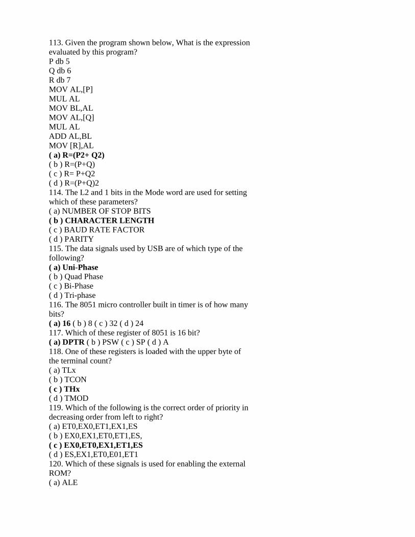
113. Given the program shown below, What is the expression
evaluated by this program?
P db 5
Q db 6
R db 7
MOV AL,[P]
MUL AL
MOV BL,AL
MOV AL,[Q]
MUL AL
ADD AL,BL
MOV [R],AL
( a) R=(P2+ Q2)
( b ) R=(P+Q)
( c ) R= P+Q2
( d ) R=(P+Q)2
114. The L2 and 1 bits in the Mode word are used for setting
which of these parameters?
( a) NUMBER OF STOP BITS
( b ) CHARACTER LENGTH
( c ) BAUD RATE FACTOR
( d ) PARITY
115. The data signals used by USB are of which type of the
following?
( a) Uni-Phase
( b ) Quad Phase
( c ) Bi-Phase
( d ) Tri-phase
116. The 8051 micro controller built in timer is of how many
bits?
( a) 16 ( b ) 8 ( c ) 32 ( d ) 24
117. Which of these register of 8051 is 16 bit?
( a) DPTR ( b ) PSW ( c ) SP ( d ) A
118. One of these registers is loaded with the upper byte of
the terminal count?
( a) TLx
( b ) TCON
( c ) THx
( d ) TMOD
119. Which of the following is the correct order of priority in
decreasing order from left to right?
( a) ET0,EX0,ET1,EX1,ES
( b ) EX0,EX1,ET0,ET1,ES,
( c ) EX0,ET0,EX1,ET1,ES
( d ) ES,EX1,ET0,E01,ET1
120. Which of these signals is used for enabling the external
ROM?
( a) ALE
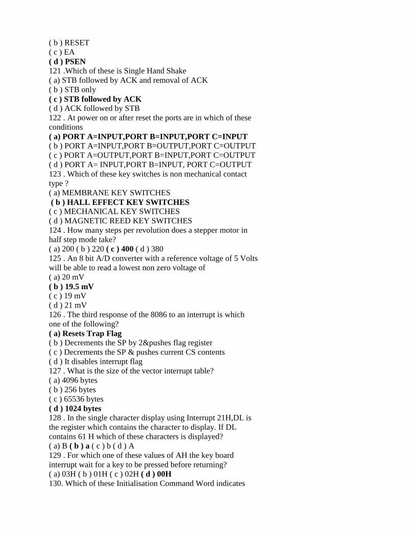
( b ) RESET
( c ) EA
( d ) PSEN
121 .Which of these is Single Hand Shake
( a) STB followed by ACK and removal of ACK
( b ) STB only
( c ) STB followed by ACK
( d ) ACK followed by STB
122 . At power on or after reset the ports are in which of these
conditions
( a) PORT A=INPUT,PORT B=INPUT,PORT C=INPUT
( b ) PORT A=INPUT,PORT B=OUTPUT,PORT C=OUTPUT
( c ) PORT A=OUTPUT,PORT B=INPUT,PORT C=OUTPUT
( d ) PORT A= INPUT,PORT B=INPUT, PORT C=OUTPUT
123 . Which of these key switches is non mechanical contact
type ?
( a) MEMBRANE KEY SWITCHES
( b ) HALL EFFECT KEY SWITCHES
( c ) MECHANICAL KEY SWITCHES
( d ) MAGNETIC REED KEY SWITCHES
124 . How many steps per revolution does a stepper motor in
half step mode take?
( a) 200 ( b ) 220 ( c ) 400 ( d ) 380
125 . An 8 bit A/D converter with a reference voltage of 5 Volts
will be able to read a lowest non zero voltage of
( a) 20 mV
( b ) 19.5 mV
( c ) 19 mV
( d ) 21 mV
126 . The third response of the 8086 to an interrupt is which
one of the following?
( a) Resets Trap Flag
( b ) Decrements the SP by 2&pushes flag register
( c ) Decrements the SP & pushes current CS contents
( d ) It disables interrupt flag
127 . What is the size of the vector interrupt table?
( a) 4096 bytes
( b ) 256 bytes
( c ) 65536 bytes
( d ) 1024 bytes
128 . In the single character display using Interrupt 21H,DL is
the register which contains the character to display. If DL
contains 61 H which of these characters is displayed?
( a) B ( b ) a ( c ) b ( d ) A
129 . For which one of these values of AH the key board
interrupt wait for a key to be pressed before returning?
( a) 03H ( b ) 01H ( c ) 02H ( d ) 00H
130. Which of these Initialisation Command Word indicates
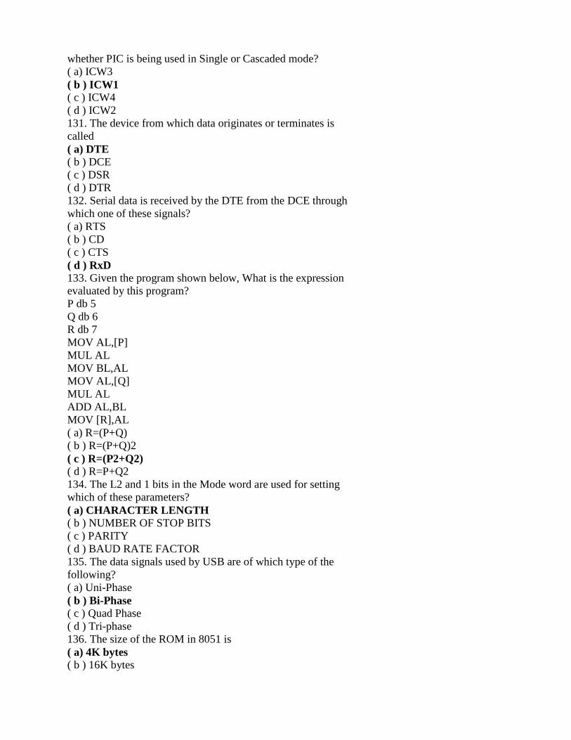
whether PIC is being used in Single or Cascaded mode?
( a) ICW3
( b ) ICW1
( c ) ICW4
( d ) ICW2
131. The device from which data originates or terminates is
called
( a) DTE
( b ) DCE
( c ) DSR
( d ) DTR
132. Serial data is received by the DTE from the DCE through
which one of these signals?
( a) RTS
( b ) CD
( c ) CTS
( d ) RxD
133. Given the program shown below, What is the expression
evaluated by this program?
P db 5
Q db 6
R db 7
MOV AL,[P]
MUL AL
MOV BL,AL
MOV AL,[Q]
MUL AL
ADD AL,BL
MOV [R],AL
( a) R=(P+Q)
( b ) R=(P+Q)2
( c ) R=(P2+Q2)
( d ) R=P+Q2
134. The L2 and 1 bits in the Mode word are used for setting
which of these parameters?
( a) CHARACTER LENGTH
( b ) NUMBER OF STOP BITS
( c ) PARITY
( d ) BAUD RATE FACTOR
135. The data signals used by USB are of which type of the
following?
( a) Uni-Phase
( b ) Bi-Phase
( c ) Quad Phase
( d ) Tri-phase
136. The size of the ROM in 8051 is
( a) 4K bytes
( b ) 16K bytes
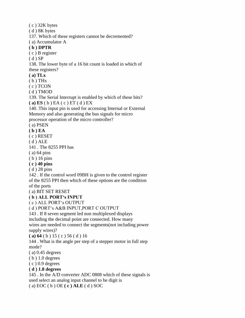
( c ) 32K bytes
( d ) 8K bytes
137. Which of these registers cannot be decremented?
( a) Accumulator A
( b ) DPTR
( c ) B register
( d ) SP
138. The lower byte of a 16 bit count is loaded in which of
these registers?
( a) TLx
( b ) THx
( c ) TCON
( d ) TMOD
139. The Serial Interrupt is enabled by which of these bits?
( a) ES ( b ) EA ( c ) ET ( d ) EX
140. This input pin is used for accessing Internal or External
Memory and also generating the bus signals for micro
processor operation of the micro controller?
( a) PSEN
( b ) EA
( c ) RESET
( d ) ALE
141 . The 8255 PPI has
( a) 64 pins
( b ) 16 pins
( c ) 40 pins
( d ) 28 pins
142 . If the control word 09BH is given to the control register
of the 8255 PPI then which of these options are the condition
of the ports
( a) BIT SET RESET
( b ) ALL PORT‘s INPUT
( c ) ALL PORT‗s OUTPUT
( d ) PORT‗s A&B INPUT,PORT C OUTPUT
143 . If 8 seven segment led non multiplexed displays
including the decimal point are connected. How many
wires are needed to connect the segments(not including power
supply wires)?
( a) 64 ( b ) 15 ( c ) 56 ( d ) 16
144 . What is the angle per step of a stepper motor in full step
mode?
( a) 0.45 degrees
( b ) 1.0 degrees
( c ) 0.9 degrees
( d ) 1.8 degrees
145 . In the A/D converter ADC 0808 which of these signals is
used select an analog input channel to be digit is
( a) EOC ( b ) OE ( c ) ALE ( d ) SOC
146 . When an interrupt service is over, what is the instruction
which makes 8086 continue executing the program it was
executing before the Interrupt occurred
( a) JMP ( b ) ESC ( c ) IRET ( d ) RET
147 . What is the offset address of INT 20H in the vector
interrupt table?
( a) 0050D
( b ) 0050H
( c ) 0080D
( d ) 0080H
148 . The DOS function AH=9 INT 21H displays a message till
which one of this character is reached
( a) × ( b ) $ ( c ) # ( d ) *
149 . Which one of these BIOS services is used for Printer
Operation?
( a) 15H ( b ) 14H ( c ) 17H ( d ) 16H
150. The PIC interrupt controller connects the single 8086 IRQ
to how many IRQ input lines?
( a) 16 ( b ) 8 ( c ) 4 ( d ) 32
151. The UART used as Serial Communication controller is
( a) 8257 ( b ) 8251 ( c ) 8250 ( d ) 8259
152. How many registers does 8251 have?
( a) 3 ( b ) 2 ( c ) 1 ( d ) 4
153. Which one of these instructions could be used for
swapping in a sort program
( a) XCHG AX,DX
( b ) SBB AX,DX
( c ) SUB AX¡ DX
( d ) MOV AX,BX
154. If B1=0 and B0=0 in the mode register of the 8251.The
USART is working in which of these modes?
( a) Synchronous mode
( b ) Asynchronous mode with BRF=16
( c ) Asynchronous mode with BRF=64
( d ) Asynchronous mode with BRF=1
155. The serial data transmission standards which uses
differential Rx & Tx signals is which one of the following?
( a) RS232C
( b ) RS449
( c ) RS423A
( d ) RS422A
156. The 8051 is a
( a) 16 bit micro controller
( b ) 24 bit micro controller
( c ) 8 bit micro controller
( d ) 32 bit micro controller
157. Which of the registers R0 to R7 support indirect
addressing?
( a) R6 & R7
( b ) R0 & R6
( c ) R0 & R7
( d ) R0 & R1
158. Which of these modes the timer is a 16 bit timer?
( a) Mode 2
( b ) Mode 3
( c ) Mode 1
( d ) Mode 0
159. The mode in which serial port operates like a shift register
is which one of the following?
( a) Mode0
( b ) Mode2
( c ) Mode3
( d ) Mode1
160. The instruction used to access data from external
memory is which one of the following?
( a) MOV @
( b ) MOV
( c ) MOVC
( d ) MOV X
161 . Group B port assignments of 8255 is
( a) Port B & Lower Port C
( b ) Port A & Upper Port C
( c ) Port B & Upper Port C
( d ) Port A & Lower Port C
162 . If the control word 00 is given to the control register of
the 8255 PPI then which of these options are the condition of
the ports
( a) BIT SET RESET
( b ) ALL PORT‗s OUTPUT
( c ) PORT‗s A&B INPUT, PORT C OUTPUT
( d ) ALL PORT‗s INPUT
163 . If 8 seven segment led non multiplexed displays
including the decimal point are all lighted up and each
of these is biased to carry 5mA.What is the total current drawn
from the power supply when all the segments
are ON?
( a) 280 mA
( b ) 40 mA
( c ) 80 mA
( d ) 320 mA
164 . The electro mechanical device which produces
mechanical displacement in proportion to an applied
voltage is know as
( a) Solenoid
( b ) Contactor
( c ) Actuator
( d ) Relay
165 . In a D/A converter the output voltage is
( a) Voltage
( b ) Pulses
( c ) current
( d ) Ramp
166 . When an interrupt service is over, what is the instruction
which makes 8086 continue executing the program it was
executing before the Interrupt occurred
( a) JMP
( b ) IRET
( c ) ESC
( d ) RET
167 . Which of these is called Break Point Interrupt?
( a) INT2
( b ) INT1
( c ) INT0
( d ) INT3
168 . Which of these values in AH performs output on video
display of Ascii character in DL?
( a) 17 ( b ) 01 ( c ) 09 ( d ) 02
169 . Which one of these BIOS services is used for Printer
Operation?
( a) 16H ( b ) 14H ( c ) 15H ( d ) 17H
170. The PIC interrupt controller which indicates that an
Interrupt is already in service is?
( a) ISR ( b ) IRR ( c ) IMR ( d ) PR
171. Communications which take place in either direction
between two systems, but can only occur in one direction at a
time is known as
( a) Complex
( b ) Half Duplex
( c ) Full Duplex
( d ) Simplex
172. The 8251 gets its clock from which of these signals?
( a) SYNDET/BD
( b ) C/D
( c ) CLK
( d ) TxC
173. Which combination of the flags indicate that the source is
equal to the destination
( a) CY=1,Z=1
( b ) CY=0,Z=0
( c ) CY=1,Z=0
( d ) CY=0,Z=1
174. Which of these bits in status register is used to clear all
errors?
( a) ER ( b ) EN ( c ) RTS ( d ) IR
175. The serial data transmission standards which uses
differential Rx& Tx signals is which one of the following?
( a) RS449
( b ) RS232C
( c ) RS423A
( d ) RS422A
176. The size of the internal data RAM in 8051 is
( a) 128 bytes
( b ) 256 bytes
( c ) 32 bytes
( d ) 1K bytes
177.Which of these register of 8051 is 16 bit?
( a) DPTR
( b ) A
( c ) PSW
( d ) SP
178. Counter or timer operation is chosen in which of these
registers?
( a) TLx
( b ) THx
( c ) TCON
( d ) TMOD
179. Which of these modes is a standard UART mode?
( a) Mode3
( b ) Mode0
( c ) Mode1
( d ) Mode2
180. The instruction used to access data from external
memory is which one of the following?
( a) MOV @
( b ) MOV
( c ) MOV X
( d ) MOVC
181 . Which of these is Double Hand Shake
( a) STB only
( b ) STB followed by ACK
( c ) STB followed by ACK and removal of ACK
( d ) ACK followed by STB
182 . At power on or after reset the ports are in which of these
conditions
( a) PORT A=INPUT,PORT B=INPUT, PORT C=INPUT
( b ) PORT A=INPUT,PORT B=INPUT, PORT C=OUT PUT
( c ) PORT A=INPUT, PORT B=OUTPUT, PORT C=OUTPUT
( d ) PORT A=OUTPUT, PORT B=INPUT, PORT C=OUTPUT
183 . Which of these Peripheral ICs is made for interfacing
Keyboards and Multiplexed LED displays?
( a) 8259 ( b ) 8237 ( c ) 8251 ( d ) 8279
184 . Which of these motors works like a digital system
( a) DC MOTOR
( b ) STEPPER MOTOR
( c ) INDUCTION MOTOR
( d ) SYNCHRONOUS MOTOR
185 . An 8 bit A/D converter with a reference voltage of 5 Volts
will be able to read a lowest non zero voltage of
( a) 20 mV ( b ) 19.5 mV ( c ) 21 mV ( d ) 19 mV
186 . The third response of the 8086 to an interrupt is which
one of the following?
( a) Decrements the SP& pushes current CS contents
( b ) Resets Trap Flag
( c ) It disables interrupt flag
( d ) Decrements the SP by 2& pushes flag register
187 . Which of these is called for doing Single Stepping?
( a) INT3
( b ) INT1
( c ) INT0
( d ) INT2
188 . In the single character display using Interrupt 21H, DL is
the register which contains the character to display. If DL
contains 41H which of these characters is displayed?
( a) A ( b ) B ( c ) b ( d ) a
189 . For which one of these values of AL does the Video
interrupt sets 80X25 color video mode?
( a) 03H ( b ) 00H ( c ) 02H ( d ) 01H
190. Which of these Initialisation Command Word indicates
whether PIC is being used in Single or Cascaded mode?
( a) ICW2
( b ) ICW4
( c ) ICW1
( d ) ICW3
191. The device from which data originates or terminates is
called
( a) DT R
( b ) DCE
( c ) DTE
( d ) DSR
192. Serial data is received by the DTE from the DCE through
which one of these signals?
( a) RxD
( b ) CD
( c ) RTS
( d ) CTS
193. Given the program shown below, What is the expression
evaluated by this program?
P db 5
Q db 6
R db 7
S db 6
MOV AL,[P]
MOV BL,[Q]
ADD AL,BL
MUL AL
ADD AL,R
MOV CL,S
DIV CL
( a) ((P+Q)2+R/S
( b ) (P+Q2+R)/s
( c ) ((P +Q)2+R)/S
( d ) ( P+(Q+R)2)/S
194. Which of these parameters are set by the S2& S1 bits?
( a) BAUD RATE FACTOR
( b ) PARITY
( c ) CHARACTER LENGTH
( d ) NUMBER OF STOP BITS
195. The data signals used by USB are of which type of the
following?
( a) Uni-Phase
( b ) Quad Phase
( c ) Bi - Phase
( d ) Tri-phase
196. The 8051 is a
( a) 24 bit micro controller
( b ) 16 bit micro controller
( c ) 8 bit micro controller
( d ) 32 bit micro controller
197. Which of these registers cannot be decremented?
( a) B register
( b ) SP
( c ) Accumulator A
( d ) DPTR
198. Which of these modes the timer is a 16 bit timer?
( a) Mode 3
( b ) Mode 0
( c ) Mode 2
( d ) Mode 1
199. The mode in which serial port operates like a shift register
is which one of the following?
( a) Mode 0
( b ) Mode 1
( c ) Mode 3
( d ) Mode 2
200. Which of these signals is used for enabling the external
ROM ?
( a) EA
( b ) RESET
( c ) ALE
( d ) PSEN
20.Tutorial classes
Hard copies will be attached
21. Known gaps
1. The MPMC subject as per the curriculum is not matching with the advance microcontrollers
like AVR,PIC and ARM.
2. As per industry applications the known gap of TTL compatible devices like RS-232,GPIB is
not present in MPMC which in the JNTU curriculum.
3. As per industry applications the known gap of DOS and BIOS Interrupts, 8259 Interrrupt
controller and DMA controller are not present in MPMC which is in JNTUH curriculum
4. As per industry applications the known gap of microprocessor real time applications are not
present in MPMC subject which in the JNTU curriculum like home applications.
Actions taken:
The following topics are taken to fill the known gaps
1.RISC vs CISC ,AVR ,ARM,PIC architectures
2. RS-2332,& GPIB
3. DOS & BIOS INTERRUPTS,8279,8257
4. Real time applications.
22. Discussion topics
UNIT 1:
o 8086 architecture
o Flag register organization
o Pin diagram of 8086
o Minimum mode and maximum mode operations
UNIT-2:
o Instruction Formats
o Addressing Modes
o Instruction Set
UNIT-3
o 8255 Architecture
o A/D and D/A Interfacing
o Keyboard/Display Interfacing
o Memory Interfacing
o Interrupt structure of 8086
o Architecture of 8251 USART
UNIT-4:
o Microcontroller architecture
o Register organization of 8051
o Memory organization
o i/0 ports
o memory interfacing
UNIT 5:
o Timer/counter operations
o Serial communication operation.
23. References, Journals, websites and E-links
Text books:-
1. Advanced Microprocessors and peripherals, A.K Ray and K.M Burch and TMH 2000
2. Micro controllers-Deshmukh, TMH
3. 8086 and 80286 microprocessors, hardware and software interfacing, -Walter A. Triebel Singh
4. Microprocessor architecture, programming and applications with 8085, by Ramesh Goankar
5. Advanced Microprocessors and Interfacing, Badri Ram, TMH
Reference Text Books:-
1. Microprocessor and interfacing-Douglas V.Hall, 2007
2. The 8088 and 8086 microprocessor-PHI, 4th Edition, 2003
3. Microcomputer systems, the 8086/8088 Family, architecture, Programming & Design, Yu-Chang Liu & Glenn
A Gibson, PHI
4. The Intel Microprocessor, 8086/8088, 80186, 80286, 80386 and 80486 programming and interfacing by Barry
B. Brey
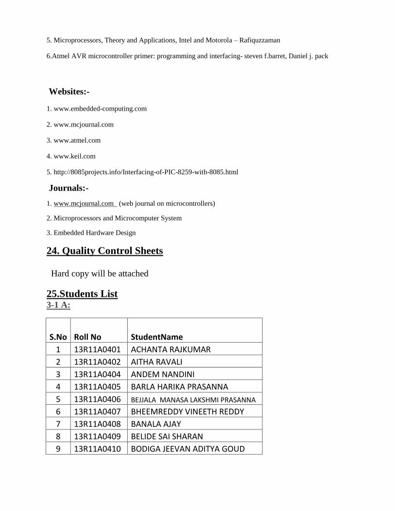
5. Microprocessors, Theory and Applications, Intel and Motorola – Rafiquzzaman
6.Atmel AVR microcontroller primer: programming and interfacing- steven f.barret, Daniel j. pack
Websites:-
1. www.embedded-computing.com
2. www.mcjournal.com
3. www.atmel.com
4. www.keil.com
5. http://8085projects.info/Interfacing-of-PIC-8259-with-8085.html
Journals:-
1. www.mcjournal.com (web journal on microcontrollers)
2. Microprocessors and Microcomputer System
3. Embedded Hardware Design
24. Quality Control Sheets
Hard copy will be attached
25.Students List 3-1 A:
S.No Roll No StudentName
1 13R11A0401 ACHANTA RAJKUMAR
2 13R11A0402 AITHA RAVALI
3 13R11A0404 ANDEM NANDINI
4 13R11A0405 BARLA HARIKA PRASANNA
5 13R11A0406 BEJJALA MANASA LAKSHMI PRASANNA
6 13R11A0407 BHEEMREDDY VINEETH REDDY
7 13R11A0408 BANALA AJAY
8 13R11A0409 BELIDE SAI SHARAN
9 13R11A0410 BODIGA JEEVAN ADITYA GOUD
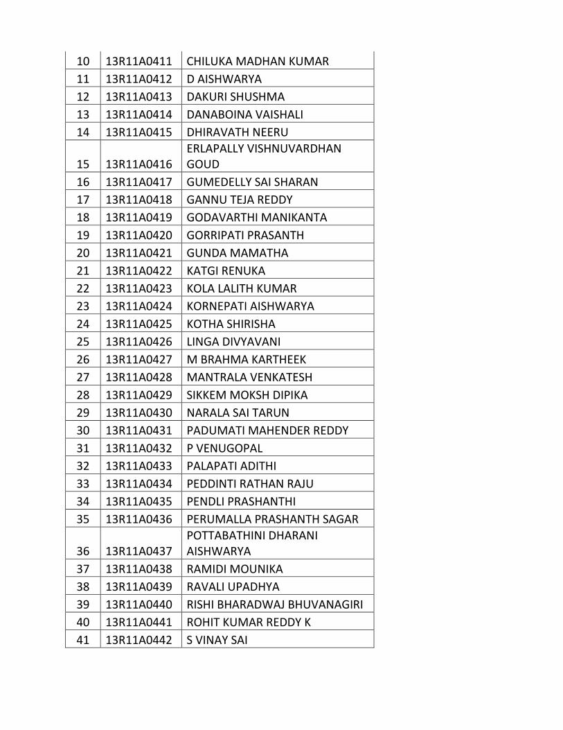
10 13R11A0411 CHILUKA MADHAN KUMAR
11 13R11A0412 D AISHWARYA
12 13R11A0413 DAKURI SHUSHMA
13 13R11A0414 DANABOINA VAISHALI
14 13R11A0415 DHIRAVATH NEERU
15 13R11A0416 ERLAPALLY VISHNUVARDHAN GOUD
16 13R11A0417 GUMEDELLY SAI SHARAN
17 13R11A0418 GANNU TEJA REDDY
18 13R11A0419 GODAVARTHI MANIKANTA
19 13R11A0420 GORRIPATI PRASANTH
20 13R11A0421 GUNDA MAMATHA
21 13R11A0422 KATGI RENUKA
22 13R11A0423 KOLA LALITH KUMAR
23 13R11A0424 KORNEPATI AISHWARYA
24 13R11A0425 KOTHA SHIRISHA
25 13R11A0426 LINGA DIVYAVANI
26 13R11A0427 M BRAHMA KARTHEEK
27 13R11A0428 MANTRALA VENKATESH
28 13R11A0429 SIKKEM MOKSH DIPIKA
29 13R11A0430 NARALA SAI TARUN
30 13R11A0431 PADUMATI MAHENDER REDDY
31 13R11A0432 P VENUGOPAL
32 13R11A0433 PALAPATI ADITHI
33 13R11A0434 PEDDINTI RATHAN RAJU
34 13R11A0435 PENDLI PRASHANTHI
35 13R11A0436 PERUMALLA PRASHANTH SAGAR
36 13R11A0437 POTTABATHINI DHARANI AISHWARYA
37 13R11A0438 RAMIDI MOUNIKA
38 13R11A0439 RAVALI UPADHYA
39 13R11A0440 RISHI BHARADWAJ BHUVANAGIRI
40 13R11A0441 ROHIT KUMAR REDDY K
41 13R11A0442 S VINAY SAI
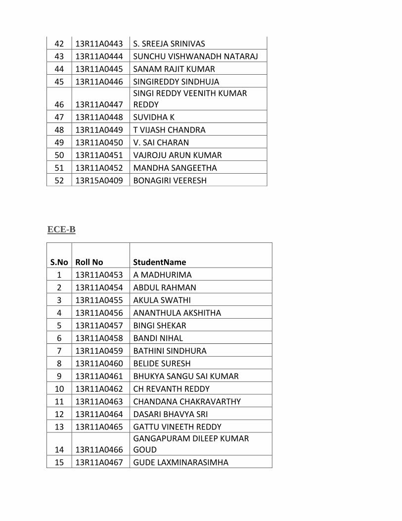
42 13R11A0443 S. SREEJA SRINIVAS
43 13R11A0444 SUNCHU VISHWANADH NATARAJ
44 13R11A0445 SANAM RAJIT KUMAR
45 13R11A0446 SINGIREDDY SINDHUJA
46 13R11A0447 SINGI REDDY VEENITH KUMAR REDDY
47 13R11A0448 SUVIDHA K
48 13R11A0449 T VIJASH CHANDRA
49 13R11A0450 V. SAI CHARAN
50 13R11A0451 VAJROJU ARUN KUMAR
51 13R11A0452 MANDHA SANGEETHA
52 13R15A0409 BONAGIRI VEERESH
ECE-B
S.No Roll No StudentName
1 13R11A0453 A MADHURIMA
2 13R11A0454 ABDUL RAHMAN
3 13R11A0455 AKULA SWATHI
4 13R11A0456 ANANTHULA AKSHITHA
5 13R11A0457 BINGI SHEKAR
6 13R11A0458 BANDI NIHAL
7 13R11A0459 BATHINI SINDHURA
8 13R11A0460 BELIDE SURESH
9 13R11A0461 BHUKYA SANGU SAI KUMAR
10 13R11A0462 CH REVANTH REDDY
11 13R11A0463 CHANDANA CHAKRAVARTHY
12 13R11A0464 DASARI BHAVYA SRI
13 13R11A0465 GATTU VINEETH REDDY
14 13R11A0466 GANGAPURAM DILEEP KUMAR GOUD
15 13R11A0467 GUDE LAXMINARASIMHA

16 13R11A0468 GAINI S PRAVEEN KUMAR
17 13R11A0469 GUNJI RAVI DEVA RAJ
18 13R11A0470 GUNTUKA PRANAYA
19 13R11A0471 KANUKOLLU S V S RAMANA KIRAN
20 13R11A0472 KOUDDEVI SUDHAKAR
21 13R11A0473 KURUSALI SREE NIDHI
22 13R11A0474 LINGAMPALLI VIVEKAR
23 13R11A0475 MARTHA MOUNIKA
24 13R11A0476 M SRINIDHI
25 13R11A0477 MALLESWARAPU VINUSHA
26 13R11A0478 MONICA JADHAV
27 13R11A0479 MUTHALE ANIL
28 13R11A0480 N MAHITHA REDDY
29 13R11A0481 N YAMINI
30 13R11A0482 NIDAMANURI SAMEERA
31 13R11A0483 NIKHILA BADDAM
32 13R11A0484 PHATALE AKSHAY KUMAR
33 13R11A0485 P PRIYANKA
34 13R11A0486 PV GAYATHRI
35 13R11A0487 PATHI VENKATESH
36 13R11A0488 PONDUGULA BHARGAVI
37 13R11A0489 POTHIREDDY ANUSHA
38 13R11A0490 RENJU K R
39 13R11A0491 S ASHWITH REDDY
40 13R11A0492 SARITA KUMARI
41 13R11A0493 GAYATRI T
42 13R11A0494 T SUMA
43 13R11A0495 TALARI NEETHIKA
44 13R11A0496 V ANJANI KUMAR
45 13R11A0497 V S SRINATH
46 13R11A0498 VANGETI AMULYA REDDY
47 13R11A0499 VEERA ABHINAY GOUD
48 13R11A04A0 PAIDIPALA ANUSHA
49 13R11A04A1 RUDHRA RAJU SAI SUMANTH
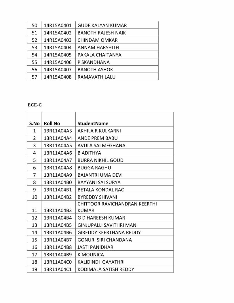
50 14R15A0401 GUDE KALYAN KUMAR
51 14R15A0402 BANOTH RAJESH NAIK
52 14R15A0403 CHINDAM OMKAR
53 14R15A0404 ANNAM HARSHITH
54 14R15A0405 PAKALA CHAITANYA
55 14R15A0406 P SKANDHANA
56 14R15A0407 BANOTH ASHOK
57 14R15A0408 RAMAVATH LALU
ECE-C
S.No Roll No StudentName
1 13R11A04A3 AKHILA R KULKARNI
2 13R11A04A4 ANDE PREM BABU
3 13R11A04A5 AVULA SAI MEGHANA
4 13R11A04A6 B ADITHYA
5 13R11A04A7 BURRA NIKHIL GOUD
6 13R11A04A8 BUGGA RAGHU
7 13R11A04A9 BAJANTRI UMA DEVI
8 13R11A04B0 BAYYANI SAI SURYA
9 13R11A04B1 BETALA KONDAL RAO
10 13R11A04B2 BYREDDY SHIVANI
11 13R11A04B3 CHITTOOR RAVICHANDRAN KEERTHI KUMAR
12 13R11A04B4 G D HAREESH KUMAR
13 13R11A04B5 GINJUPALLI SAVITHRI MANI
14 13R11A04B6 GIREDDY KEERTHANA REDDY
15 13R11A04B7 GONURI SIRI CHANDANA
16 13R11A04B8 JASTI PANIDHAR
17 13R11A04B9 K MOUNICA
18 13R11A04C0 KALIDINDI GAYATHRI
19 13R11A04C1 KODIMALA SATISH REDDY
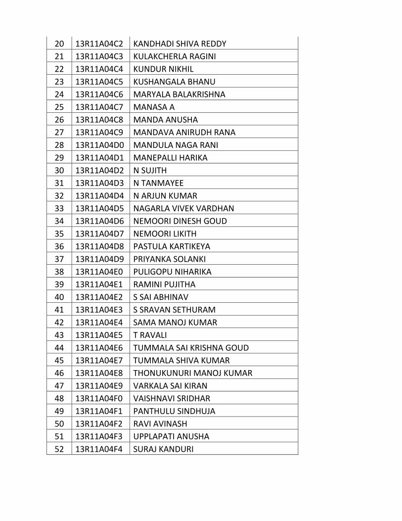
20 13R11A04C2 KANDHADI SHIVA REDDY
21 13R11A04C3 KULAKCHERLA RAGINI
22 13R11A04C4 KUNDUR NIKHIL
23 13R11A04C5 KUSHANGALA BHANU
24 13R11A04C6 MARYALA BALAKRISHNA
25 13R11A04C7 MANASA A
26 13R11A04C8 MANDA ANUSHA
27 13R11A04C9 MANDAVA ANIRUDH RANA
28 13R11A04D0 MANDULA NAGA RANI
29 13R11A04D1 MANEPALLI HARIKA
30 13R11A04D2 N SUJITH
31 13R11A04D3 N TANMAYEE
32 13R11A04D4 N ARJUN KUMAR
33 13R11A04D5 NAGARLA VIVEK VARDHAN
34 13R11A04D6 NEMOORI DINESH GOUD
35 13R11A04D7 NEMOORI LIKITH
36 13R11A04D8 PASTULA KARTIKEYA
37 13R11A04D9 PRIYANKA SOLANKI
38 13R11A04E0 PULIGOPU NIHARIKA
39 13R11A04E1 RAMINI PUJITHA
40 13R11A04E2 S SAI ABHINAV
41 13R11A04E3 S SRAVAN SETHURAM
42 13R11A04E4 SAMA MANOJ KUMAR
43 13R11A04E5 T RAVALI
44 13R11A04E6 TUMMALA SAI KRISHNA GOUD
45 13R11A04E7 TUMMALA SHIVA KUMAR
46 13R11A04E8 THONUKUNURI MANOJ KUMAR
47 13R11A04E9 VARKALA SAI KIRAN
48 13R11A04F0 VAISHNAVI SRIDHAR
49 13R11A04F1 PANTHULU SINDHUJA
50 13R11A04F2 RAVI AVINASH
51 13R11A04F3 UPPLAPATI ANUSHA
52 13R11A04F4 SURAJ KANDURI

ECE-D
S.No Roll No StudentName
1 13R11A04F5 A RAMA THEJA
2 13R11A04F7 ANUGU PRASHANTH
3 13R11A04F8 ARACHANA DASH
4 13R11A04F9 CHAVALI NAGARJUNA
5 13R11A04G0 CHIGURUPATI MEENAKSHI
6 13R11A04G1 D SRI RAMYA
7 13R11A04G2 DEEKONDA RAJSHREE
8 13R11A04G3 G MANIDEEP
9 13R11A04G4 GATADI VADDE PREM SAGAR
10 13R11A04G5 GOGU JEEVITHA SPANDANA REDDY
11 13R11A04G6 GOLLURI SINDHUJA
12 13R11A04G7 GOPANABOENA SAI KRANTHI KUMAR
13 13R11A04G8 GUNTIMADUGU SAI RESHMA
14 13R11A04G9 K DARSHAN
15 13R11A04H0 K. ANIRUDH
16 13R11A04H1 KOMIRISHETTY AKHILA
17 13R11A04H2 KOPPU MOUNIKA
18 13R11A04H3 KANNE RAVI KUMAR
19 13R11A04H4 KARRA VINEELA
20 13R11A04H5 KANUKALA SIDDHARTH
21 13R11A04H6 KATHI SHIVARAM REDDY
22 13R11A04H7 KOMANDLA SRIKANTH REDDY
23 13R11A04H8 KONDAM PADMA
24 13R11A04H9 KRISHNA ASHOK MORE
25 13R11A04J0 LINGAMPALLY RAJASRI
26 13R11A04J1 M ROHITH SAI SHASHANK
27 13R11A04J2 M TANVIKA
28 13R11A04J3 MALIHA AZAM
29 13R11A04J4 MANSHA NEYAZ
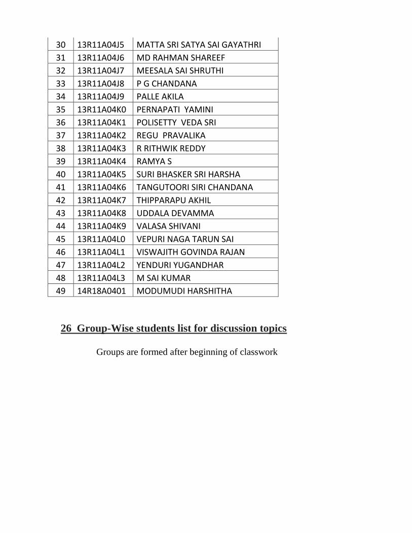
30 13R11A04J5 MATTA SRI SATYA SAI GAYATHRI
31 13R11A04J6 MD RAHMAN SHAREEF
32 13R11A04J7 MEESALA SAI SHRUTHI
33 13R11A04J8 P G CHANDANA
34 13R11A04J9 PALLE AKILA
35 13R11A04K0 PERNAPATI YAMINI
36 13R11A04K1 POLISETTY VEDA SRI
37 13R11A04K2 REGU PRAVALIKA
38 13R11A04K3 R RITHWIK REDDY
39 13R11A04K4 RAMYA S
40 13R11A04K5 SURI BHASKER SRI HARSHA
41 13R11A04K6 TANGUTOORI SIRI CHANDANA
42 13R11A04K7 THIPPARAPU AKHIL
43 13R11A04K8 UDDALA DEVAMMA
44 13R11A04K9 VALASA SHIVANI
45 13R11A04L0 VEPURI NAGA TARUN SAI
46 13R11A04L1 VISWAJITH GOVINDA RAJAN
47 13R11A04L2 YENDURI YUGANDHAR
48 13R11A04L3 M SAI KUMAR
49 14R18A0401 MODUMUDI HARSHITHA
26 Group-Wise students list for discussion topics
Groups are formed after beginning of classwork