Unit-8 mpmc
31
Unit-VIII ARM 32 Bit MCUs Introduction to 16/32 Bit processors – ARM architecture and organization – ARM / Thumb programming model – ARM / Thumb instruction set – Development tools. A1.1 About the ARM architecture The ARM architecture has evolved to a point where it supports implementations across a wide spectrum of performance points. Over two billion parts have shipped, establishing it as the dominant architecture across many market segments. The architectural simplicity of ARM processors has traditionally led to very small implementations, and small implementations allow devices with very low power consumption. Implementation size, performance, and very low power consumption remain key attributes in the development of the ARM architecture. The ARM is a Reduced Instruction Set Computer (RISC), as it incorporates these typical RISC architecture features: • a large uniform register file • a load/store architecture, where data-processing operations only operate on register contents, not directly on memory contents • simple addressing modes, with all load/store addresses being determined from register contents and instruction fields only • uniform and fixed-length instruction fields, to simplify instruction decode. In addition, the ARM architecture provides: • control over both the Arithmetic Logic Unit (ALU) and shifter in most data-processing instructions to maximize the use of an ALU and a shifter • auto-increment and auto-decrement addressing modes to optimize program loops • Load and Store Multiple instructions to maximize data throughput
-
Upload
mani-kanta-reddy -
Category
Documents
-
view
181 -
download
5
Transcript of Unit-8 mpmc
Unit-VIII
ARM 32 Bit MCUs
Introduction to 16/32 Bit processors – ARM architecture and organization – ARM / Thumb programming model – ARM / Thumb instruction set – Development tools.
A1.1 About the ARM architectureThe ARM architecture has evolved to a point where it supports implementations across a wide spectrum of performance points. Over two billion parts have shipped, establishing it as the dominant architecture across many market segments. The architectural simplicity of ARM processors has traditionally led to very small implementations, and small implementations allow devices with very low power consumption. Implementation size, performance, and very low power consumption remain key attributes in the development of the ARM architecture.The ARM is a Reduced Instruction Set Computer (RISC), as it incorporates these typical RISC architecturefeatures:• a large uniform register file• a load/store architecture, where data-processing operations only operate on register contents, notdirectly on memory contents• simple addressing modes, with all load/store addresses being determined from register contents andinstruction fields only• uniform and fixed-length instruction fields, to simplify instruction decode.In addition, the ARM architecture provides:• control over both the Arithmetic Logic Unit (ALU) and shifter in most data-processing instructionsto maximize the use of an ALU and a shifter• auto-increment and auto-decrement addressing modes to optimize program loops• Load and Store Multiple instructions to maximize data throughput• conditional execution of almost all instructions to maximize execution throughput.These enhancements to a basic RISC architecture allow ARM processors to achieve a good balance of highperformance, small code size, low power consumption, and small silicon area.
ARM7 internals
Core block diagram
A1.1.1 ARM registers

ARM has 31 general-purpose 32-bit registers. At any one time, 16 of these registers are visible. The otherregisters are used to speed up exception processing. All the register specifiers in ARM instructions canaddress any of the 16 visible registers.The main bank of 16 registers is used by all unprivileged code. These are the User mode registers. Usermode is different from all other modes as it is unprivileged, which means:• User mode can only switch to another processor mode by generating an exception. The SWIinstruction provides this facility from program control.• Memory systems and coprocessors might allow User mode less access to memory and coprocessorfunctionality than a privileged mode.Three of the 16 visible registers have special roles:Stack pointer Software normally uses R13 as a Stack Pointer (SP). R13 is used by the PUSH and POPinstructions in T variants, and by the SRS and RFE instructions from ARMv6.Link register Register 14 is the Link Register (LR). This register holds the address of the nextinstruction after a Branch and Link (BL or BLX) instruction, which is the instructionused to make a subroutine call. It is also used for return address information on entryto exception modes. At all other times, R14 can be used as a general-purposeregister.Program counter Register 15 is the Program Counter (PC). It can be used in most instructions asa pointer to the instruction which is two instructions after the instruction beingexecuted. In ARM state, all ARM instructions are four bytes long (one 32-bit word)and are always aligned on a word boundary. This means that the bottom two bits ofthe PC are always zero, and therefore the PC contains only 30 non-constant bits.Two other processor states are supported by some versions of the architecture.Thumb® state is supported on T variants, and Jazelle® state on J variants. The PC canbe halfword (16-bit) and byte aligned respectively in these states.The remaining 13 registers have no special hardware purpose. Their uses are defined purely by software.For more details on registers, refer to Registers on page A2-4.
A1.1.2 ExceptionsARM supports seven types of exception, and a privileged processing mode for each type. The seven typesof exception are:• reset• attempted execution of an Undefined instruction• software interrupt (SWI) instructions, can be used to make a call to an operating system• Prefetch Abort, an instruction fetch memory abort• Data Abort, a data access memory abort• IRQ, normal interrupt• FIQ, fast interrupt.
When an exception occurs, some of the standard registers are replaced with registers specific to theexception mode. All exception modes have replacement banked registers for R13 and R14. The fastinterrupt mode has additional banked registers for fast interrupt processing.When an exception handler is entered, R14 holds the return address for exception processing. This is usedto return after the exception is processed and to address the instruction that caused the exception.Register 13 is banked across exception modes to provide each exception handler with a private stack pointer.The fast interrupt mode also banks registers 8 to 12 so that interrupt processing can begin without the needto save or restore these registers.There is a sixth privileged processing mode, System mode, which uses the User mode registers. This is usedto run tasks that require privileged access to memory and/or coprocessors, without limitations on whichexceptions can occur during the task.In addition to the above, reset shares the same privileged mode as SWIs.For more details on exceptions, refer to Exceptions on page A2-16.The exception processWhen an exception occurs, the ARM processor halts execution in a defined manner and begins execution atone of a number of fixed addresses in memory, known as the exception vectors. There is a separate vectorlocation for each exception, including reset. Behavior is defined for normal running systems (see sectionA2.6) and debug events (see Chapter D3 Coprocessor 14, the Debug Coprocessor)An operating system installs a handler on every exception at initialization. Privileged operating system tasksare normally run in System mode to allow exceptions to occur within the operating system without state loss.Introduction
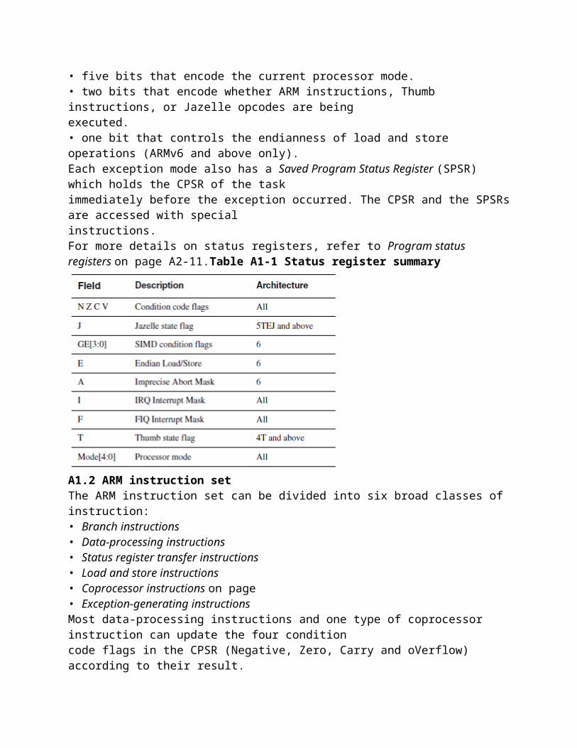
A1.1.3 Status registersAll processor state other than the general-purpose register contents is held in status registers. The currentoperating processor status is in the Current Program Status Register (CPSR). The CPSR holds:• four condition code flags (Negative, Zero, Carry and oVerflow).• one sticky (Q) flag (ARMv5 and above only). This encodes whether saturation has occurred insaturated arithmetic instructions, or signed overflow in some specific multiply accumulateinstructions.• four GE (Greater than or Equal) flags (ARMv6 and above only). These encode the followingconditions separately for each operation in parallel instructions:— whether the results of signed operations were non-negative— whether unsigned operations produced a carry or a borrow.• two interrupt disable bits, one for each type of interrupt (two in ARMv5 and below).
• one (A) bit imprecise abort mask (from ARMv6)• five bits that encode the current processor mode.• two bits that encode whether ARM instructions, Thumb instructions, or Jazelle opcodes are beingexecuted.• one bit that controls the endianness of load and store operations (ARMv6 and above only).Each exception mode also has a Saved Program Status Register (SPSR) which holds the CPSR of the taskimmediately before the exception occurred. The CPSR and the SPSRs are accessed with specialinstructions.For more details on status registers, refer to Program status registers on page A2-11.Table A1-1 Status register summary
A1.2 ARM instruction setThe ARM instruction set can be divided into six broad classes of instruction:• Branch instructions• Data-processing instructions • Status register transfer instructions • Load and store instructions • Coprocessor instructions on page • Exception-generating instructionsMost data-processing instructions and one type of coprocessor instruction can update the four conditioncode flags in the CPSR (Negative, Zero, Carry and oVerflow) according to their result.Almost all ARM instructions contain a 4-bit condition field. One value of this field specifies that theinstruction is executed unconditionally.Fourteen other values specify conditional execution of the instruction. If the condition code flags indicatethat the corresponding condition is true when the instruction starts executing, it executes normally.Otherwise, the instruction does nothing. The 14 available conditions allow:
• tests for equality and non-equality• tests for <, <=, >, and >= inequalities, in both signed and unsigned arithmetic• each condition code flag to be tested individually.The sixteenth value of the condition field encodes alternative instructions. These do not allow conditionalexecution. Before ARMv5 these instructions were UNPREDICTABLE.
A1.2.1 Branch instructionsAs well as allowing many data-processing or load instructions to change control flow by writing the PC, astandard Branch instruction is provided with a 24-bit signed word offset, allowing forward and backwardbranches of up to 32MB.There is a Branch and Link (BL) option that also preserves the address of the instruction after the branch inR14, the LR. This provides a subroutine call which can be returned from by copying the LR into the PC.There are also branch instructions which can switch instruction set, so that execution continues at the branchtarget using the Thumb instruction set or Jazelle opcodes. Thumb support allows ARM code to call Thumbsubroutines, and ARM subroutines to return to a Thumb caller. Similar instructions in the Thumb instructionset allow the corresponding Thumb → ARM switches. An overview of the Thumb instruction set isprovided in Chapter A6 The Thumb Instruction Set.The BXJ instruction introduced with the J variant of ARMv5, and present in ARMv6, provides thearchitected mechanism for entry to Jazelle state, and the associated assertion of the J flag in the CPSR.A1.2.2 Data-processing instructionsThe data-processing instructions perform calculations on the general-purpose registers. There are five typesof data-processing instructions:• Arithmetic/logic instructions• Comparison instructions• Single Instruction Multiple Data (SIMD) instructions• Multiply instructions on page A1-8• Miscellaneous Data Processing instructions on page A1-8.Arithmetic/logic instructionsThe following arithmetic/logic instructions share a common instruction format. These perform an arithmeticor logical operation on up to two source operands, and write the result to a destination register. They canalso optionally update the condition code flags, based on the result.
Of the two source operands:• one is always a register• the other has two basic forms:— an immediate value— a register value, optionally shifted.If the operand is a shifted register, the shift amount can be either an immediate value or the value of anotherregister. Five types of shift can be specified. Every arithmetic/logic instruction can therefore perform anarithmetic/logic operation and a shift operation. As a result, ARM does not have dedicated shift instructions.The Program Counter (PC) is a general-purpose register, and therefore arithmetic/logic instructions canwrite their results directly to the PC. This allows easy implementation of a variety of jump instructions.Comparison instructionsThe comparison instructions use the same instruction format as the arithmetic/logic instructions. Theseperform an arithmetic or logical operation on two source operands, but do not write the result to a register.They always update the condition flags, based on the result.The source operands of comparison instructions take the same forms as those of arithmetic/logicinstructions, including the ability to incorporate a shift operation.Single Instruction Multiple Data (SIMD) instructionsThe add and subtract instructions treat each operand as two parallel 16-bit numbers, or four parallel 8-bitnumbers. They can be treated as signed or unsigned. The operations can optionally be saturating, wraparound, or the results can be halved to avoid overflow.These instructions are available in ARMv6.Multiply instructionsThere are several classes of multiply instructions, introduced at different times into the architecture. SeeMultiply instructions on page A3-10 for details.Miscellaneous Data Processing instructionsThese include Count Leading Zeros (CLZ) and Unsigned Sum of Absolute Differences with optionalAccumulate (USAD8 and USADA8).A1.2.3 Status register transfer instructionsThe status register transfer instructions transfer the contents of the CPSR or an SPSR to or from ageneral-purpose register. Writing to the CPSR can:• set the values of the condition code flags• set the values of the interrupt enable bits• set the processor mode and state• alter the endianness of Load and Store operations.
A1.2.4 Load and store instructionsThe following load and store instructions are available:• Load and Store Register• Load and Store Multiple registers on page A1-9• Load and Store Register Exclusive on page A1-9.There are also swap and swap byte instructions, but their use is deprecated in ARMv6. It is recommendedthat all software migrates to using the load and store register exclusive instructions.Load and Store RegisterLoad Register instructions can load a 64-bit doubleword, a 32-bit word, a 16-bit halfword, or an 8-bit bytefrom memory into a register or registers. Byte and halfword loads can be automatically zero-extended orsign-extended as they are loaded.Store Register instructions can store a 64-bit doubleword, a 32-bit word, a 16-bit halfword, or an 8-bit bytefrom a register or registers to memory.From ARMv6, unaligned loads and stores of words and halfwords are supported, accessing the specifiedbyte addresses. Prior to ARMv6, unaligned 32-bit loads rotated data, all 32-bit stores were aligned, and theother affected instructions UNPREDICTABLE.Load and Store Register instructions have three primary addressing modes, all of which use a base registerand an offset specified by the instruction:• In offset addressing, the memory address is formed by adding or subtracting an offset to or from thebase register value.• In pre-indexed addressing, the memory address is formed in the same way as for offset addressing.As a side effect, the memory address is also written back to the base register.• In post-indexed addressing, the memory address is the base register value. As a side effect, an offsetis added to or subtracted from the base register value and the result is written back to the base register.In each case, the offset can be either an immediate or the value of an index register. Register-based offsetscan also be scaled with shift operations.As the PC is a general-purpose register, a 32-bit value can be loaded directly into the PC to perform a jumpto any address in the 4GB memory space.Load and Store Multiple registersLoad Multiple (LDM) and Store Multiple (STM) instructions perform a block transfer of any number ofthe general-purpose registers to or from memory. Four addressing modes are provided:• pre-increment
• post-increment• pre-decrement• post-decrement.The base address is specified by a register value, which can be optionally updated after the transfer. As thesubroutine return address and PC values are in general-purpose registers, very efficient subroutine entry andexit sequences can be constructed with LDM and STM:• A single STM instruction at subroutine entry can push register contents and the return address onto thestack, updating the stack pointer in the process.• A single LDM instruction at subroutine exit can restore register contents from the stack, load the PCwith the return address, and update the stack pointer.LDM and STM instructions also allow very efficient code for block copies and similar data movementalgorithms.Load and Store Register ExclusiveThese instructions support cooperative memory synchronization. They are designed to provide the atomicbehavior required for semaphores without locking all system resources between the load and store phases.See LDREX on page A4-52 and STREX on page A4-202 for details.A1.2.5 Coprocessor instructionsThere are three types of coprocessor instructions:Data-processing instructionsThese start a coprocessor-specific internal operation.Data transfer instructionsThese transfer coprocessor data to or from memory. The address of the transfer is calculatedby the ARM processor.Register transfer instructionsThese allow a coprocessor value to be transferred to or from an ARM register, or a pair ofARM registers.A1.2.6 Exception-generating instructionsTwo types of instruction are designed to cause specific exceptions to occur.Software interrupt instructionsSWI instructions cause a software interrupt exception to occur. These are normally used tomake calls to an operating system, to request an OS-defined service. The exception entrycaused by a SWI instruction also changes to a privileged processor mode. This allows anunprivileged task to gain access to privileged functions, but only in ways permitted by theOS.Software breakpoint instructionsBKPT instructions cause an abort exception to occur. If suitable debugger software is installedon the abort vector, an abort exception generated in this fashion is treated as a breakpoint.If debug hardware is present in the system, it can instead treat a BKPT instruction directly asa breakpoint, preventing the abort exception from occurring.
In addition to the above, the following types of instruction cause an Undefined Instruction exception tooccur:• coprocessor instructions which are not recognized by any hardware coprocessor• most instruction words that have not yet been allocated a meaning as an ARM instruction.In each case, this exception is normally used either to generate a suitable error or to initiate softwareemulation of the instruction.A2.1 Data typesARM processors support the following data types:Byte 8 bitsHalfword 16 bitsWord 32 bitsNote• Support for halfwords was introduced in version 4.• ARMv6 has introduced unaligned data support for words and halfwords. See Unaligned accesssupport on page A2-38 for more information.• When any of these types is described as unsigned, the N-bit data value represents a non-negativeinteger in the range 0 to +2N-1, using normal binary format.• When any of these types is described as signed, the N-bit data value represents an integer in the range-2N-1 to +2N-1-1, using two's complement format.• Most data operations, for example ADD, are performed on word quantities. Long multiplies support64-bit results with or without accumulation. ARMv5TE introduced some halfword multiplyoperations. ARMv6 introduced a variety of Single Instruction Multiple Data (SIMD) instructionsoperating on two halfwords or four bytes in parallel.• Load and store operations can transfer bytes, halfwords, or words to and from memory, automaticallyzero-extending or sign-extending bytes or halfwords as they are loaded. Load and store operationsthat transfer two or more words to and from memory are also provided.• ARM instructions are exactly one word and are aligned on a four-byte boundary. Thumb® instructionsare exactly one halfword and are aligned on a two-byte boundary. Jazelle® opcodes are a variablenumber of bytes in length and can appear at any byte alignment.
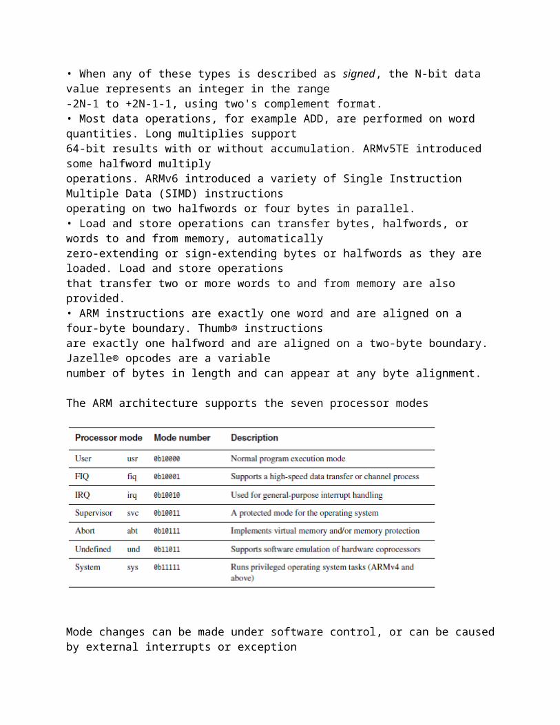
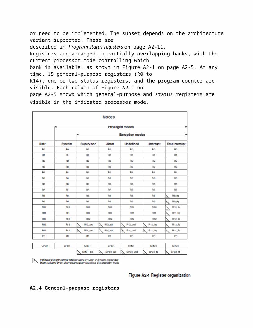
The ARM architecture supports the seven processor modes
Mode changes can be made under software control, or can be caused by external interrupts or exceptionprocessing.Most application programs execute in User mode. When the processor is in User mode, the program beingexecuted is unable to access some protected system resources or to change mode, other than by causing anexception to occur (see Exceptions on page A2-16). This allows a suitably-written operating system tocontrol the use of system resources.The modes other than User mode are known as privileged modes. They have full access to system resourcesand can change mode freely. Five of them are known as exception modes:• FIQ• IRQ• Supervisor• Abort• Undefined.These are entered when specific exceptions occur. Each of them has some additional registers to avoidcorrupting User mode state when the exception occurs (see Registers on page A2-4 for details).The remaining mode is System mode, which is not entered by any exception and has exactly the sameregisters available as User mode. However, it is a privileged mode and is therefore not subject to the Usermode restrictions. It is intended for use by operating system tasks that need access to system resources, butwish to avoid using the additional registers associated with the exception modes. Avoiding such use ensuresthat the task state is not corrupted by the occurrence of any exception.
A2.3 RegistersThe ARM processor has a total of 37 registers:• Thirty-one general-purpose registers, including a program counter. These registers are 32 bits wideand are described in General-purpose registers on page A2-6.• Six status registers. These registers are also 32 bits wide, but only some of the 32 bits are allocatedor need to be implemented. The subset depends on the architecture variant supported. These aredescribed in Program status registers on page A2-11.Registers are arranged in partially overlapping banks, with the current processor mode controlling whichbank is available, as shown in Figure A2-1 on page A2-5. At any time, 15 general-purpose registers (R0 toR14), one or two status registers, and the program counter are visible. Each column of Figure A2-1 onpage A2-5 shows which general-purpose and status registers are visible in the indicated processor mode.
A2.4 General-purpose registersThe general-purpose registers R0 to R15 can be split into three groups. These groups differ in the way theyare banked and in their special-purpose uses:• The unbanked registers, R0 to R7• The banked registers, R8 to R14• Register 15, the PC, is described in Register 15 and the program counter on page A2-9.A2.4.1 The unbanked registers, R0 to R7Registers R0 to R7 are unbanked registers. This means that each of them refers to the same 32-bit physicalregister in all processor modes. They are completely general-purpose registers, with no special uses impliedby the architecture, and can be used wherever an instruction allows a general-purpose register to bespecified.A2.4.2 The banked registers, R8 to R14
Registers R8 to R14 are banked registers. The physical register referred to by each of them depends on thecurrent processor mode. Where a particular physical register is intended, without depending on the currentprocessor mode, a more specific name (as described below) is used. Almost all instructions allow the bankedregisters to be used wherever a general-purpose register is allowed.NoteThere are a few exceptions to this rule for processors pre-ARMv6, and they are noted in the individualinstruction descriptions. Where a restriction exists on the use of banked registers, it always applies to all ofR8 to R14. For example, R8 to R12 are subject to such restrictions even in systems in which FIQ mode isnever used and so only one physical version of the register is ever in use.Registers R8 to R12 have two banked physical registers each. One is used in all processor modes other thanFIQ mode, and the other is used in FIQ mode. Where it is necessary to be specific about which version isbeing referred to, the first group of physical registers are referred to as R8_usr to R12_usr and the secondgroup as R8_fiq to R12_fiq.Registers R8 to R12 do not have any dedicated special purposes in the architecture. However, for interruptsthat are simple enough to be processed using registers R8 to R14 only, the existence of separate FIQ modeversions of these registers allows very fast interrupt processing.Registers R13 and R14 have six banked physical registers each. One is used in User and System modes, andeach of the remaining five is used in one of the five exception modes. Where it is necessary to be specificabout which version is being referred to, you use names of the form:R13_<mode>R14_<mode>where <mode> is the appropriate one of usr, svc (for Supervisor mode), abt, und, irq and fiq.
Register R13 is normally used as a stack pointer and is also known as the SP. The SRS instruction, introducedin ARMv6, is the only ARM instruction that uses R13 in a special-case manner. There are other suchinstructions in the Thumb instruction set, as described in Chapter A6 The Thumb Instruction Set.Each exception mode has its own banked version of R13. Suitable uses for these banked versions of R13depend on the architecture version:• In architecture versions earlier than ARMv6, each banked version of R13 will normally be initialized
to point to a stack dedicated to that exception mode. On entry, the exception handler typically storesthe values of other registers that it wants to use on this stack. By reloading these values into theregister when it returns, the exception handler can ensure that it does not corrupt the state of theprogram that was being executed when the exception occurred.If fewer exception-handling stacks are desired in a system than this implies, it is possible instead toinitialize the banked version of R13 for an exception mode to point to a small area of memory that isused for temporary storage while transferring to another exception mode and its stack. For example,suppose that there is a requirement for an IRQ handler to use the Supervisor mode stack to storeSPSR_irq, R0 to R3, R12, R14_irq, and then to execute in Supervisor mode with IRQs enabled. Thiscan be achieved by initializing R13_irq to point to a four-word temporary storage area, and using thefollowing code sequence on entry to the handler:STMIA R13, (R0-R3) ; Put R0-R3 into temporary storageMRS R0, SPSR ; Move banked SPSR and R12-R14 intoMOV R1, R12 ; unbanked registersMOV R2, R13MOV R3, R14MRS R12, CPSR ; Use read/modify/write sequenceBIC R12, R12, #0x1F ; on CPSR to switch to SupervisorORR R12, R12, #0x13 ; modeMSR CPSR_c, R12STMFD R13!, (R1,R3) ; Push original {R12, R14_irq}, thenSTR R0, [R13,#-20]! ; SPSR_irq with a gap for R0-R3LDMIA R2, {R0-R3} ; Reload R0-R3 from temporary storageBIC R12, R12, #0x80 ; Modify and write CPSR again toMSR CPSR_c, R12 ; re-enable IRQsSTMIB R13, {R0-R3} ; Store R0-R3 in the gap left on the; stack for them• In ARMv6 and above, it is recommended that the OS designer should decide how manyexception-handling stacks are required in the system, and select a suitable processor mode in whichto handle the exceptions that use each stack. For example, one exception-handling stack might berequired to be locked into real memory and be used for aborts and high-priority interrupts, whileanother could use virtual memory and be used for SWIs, Undefined instructions and low-priorityinterrupts. Suitable processor modes in this example might be Abort mode and Supervisor moderespectively.The banked version of R13 for each of the selected modes is then initialized to point to thecorresponding stack, and the other banked versions of R13 are normally not used. Each exceptionhandler starts with an SRS instruction to store the exception return information to the appropriate
stack, followed (if necessary) by a CPS instruction to switch to the appropriate mode and possibly
re-enable interrupts, after which other registers can be saved on that stack. So in the above example,an Undefined Instruction handler that wants to re-enable interrupts immediately would start with thefollowing two instructions:SRSFD #svc_mode!CPSIE i, #svc_modeThe handler can then operate entirely in Supervisor mode, using the virtual memory stack pointed toby R13_svc.Register R14 (also known as the Link Register or LR) has two special functions in the architecture:• In each mode, the mode's own version of R14 is used to hold subroutine return addresses. When asubroutine call is performed by a BL or BLX instruction, R14 is set to the subroutine return address. Thesubroutine return is performed by copying R14 back to the program counter. This is typically donein one of the two following ways:— Execute a BX LR instruction.NoteAn MOV PC,LR instruction will perform the same function as BX LR if the code to which it returnsuses the current instruction set, but will not return correctly from an ARM subroutine calledby Thumb code, or from a Thumb subroutine called by ARM code. The use of MOV PC,LRinstructions for subroutine return is therefore deprecated.— On subroutine entry, store R14 to the stack with an instruction of the form:STMFD SP!,{<registers>,LR}and use a matching instruction to return:LDMFD SP!,{<registers>,PC}• When an exception occurs, the appropriate exception mode's version of R14 is set to the exceptionreturn address (offset by a small constant for some exceptions). The exception return is performed ina similar way to a subroutine return, but using slightly different instructions to ensure full restorationof the state of the program that was being executed when the exception occurred. See Exceptions onpage A2-16 for more details.Register R14 can be treated as a general-purpose register at all other times.NoteWhen nested exceptions are possible, the two special-purpose uses might conflict. For example, if an IRQ
interrupt occurs when a program is being executed in User mode, none of the User mode registers arenecessarily corrupted. But if an interrupt handler running in IRQ mode re-enables IRQ interrupts and anested IRQ interrupt occurs, any value the outer interrupt handler is holding in R14_irq at the time isoverwritten by the return address of the nested interrupt.System programmers need to be careful about such interactions. The usual way to deal with them is toensure that the appropriate version of R14 does not hold anything significant at times when nestedexceptions can occur. When this is hard to do in a straightforward way, it is usually best to change to another
processor mode during entry to the exception handler, before re-enabling interrupts or otherwise allowingnested exceptions to occur. (In ARMv4 and above, System mode is often the best mode to use for thispurpose.)A2.4.3 Register 15 and the program counterRegister R15 (R15) is often used in place of the other general-purpose registers to produce variousspecial-case effects. These are instruction-specific and so are described in the individual instructiondescriptions.There are also many instruction-specific restrictions on the use of R15. these are also noted in the individualinstruction descriptions. Usually, the instruction is UNPREDICTABLE if R15 is used in a manner that breaksthese restrictions.If an instruction description neither describes a special-case effect when R15 is used nor places restrictionson its use, R15 is used to read or write the Program Counter (PC), as described in:• Reading the program counter• Writing the program counter on page A2-10.Reading the program counterWhen an instruction reads the PC, the value read depends on which instruction set it comes from:• For an ARM instruction, the value read is the address of the instruction plus 8 bytes. Bits [1:0] of thisvalue are always zero, because ARM instructions are always word-aligned.• For a Thumb instruction, the value read is the address of the instruction plus 4 bytes. Bit [0] of thisvalue is always zero, because Thumb instructions are always halfword-aligned.This way of reading the PC is primarily used for quick, position-independent addressing of nearbyinstructions and data, including position-independent branching within a program.
An exception to the above rule occurs when an ARM STR or STM instruction stores R15. Such instructionscan store either the address of the instruction plus 8 bytes, like other instructions that read R15, or theaddress of the instruction plus 12 bytes. Whether the offset of 8 or the offset of 12 is used isIMPLEMENTATION DEFINED. An implementation must use the same offset for all ARM STR and STMinstructions that store R15. It cannot use 8 for some of them and 12 for others.Because of this exception, it is usually best to avoid the use of STR and STM instructions that store R15. If thisis difficult, use a suitable instruction sequence in the program to ascertain which offset the implementationuses. For example, if R0 points to an available word of memory, then the following instructions put the offsetof the implementation in R0:SUB R1, PC, #4 ; R1 = address of following STR instructionSTR PC, [R0] ; Store address of STR instruction + offset,LDR R0, [R0] ; then reload itSUB R0, R0, R1 ; Calculate the offset as the difference
The rules about how R15 is read apply only to reads by instructions. In particular, they do not necessarilydescribe the values placed on a hardware address bus during instruction fetches. Like all other details ofhardware interfaces, such values are IMPLEMENTATION DEFINED.Writing the program counterWhen an instruction writes the PC, the normal result is that the value written to the PC is treated as aninstruction address and a branch occurs to that address.Since ARM instructions are required to be word-aligned, values they write to the PC are normally expectedto have bits[1:0] == 0b00. Similarly, Thumb instructions are required to be halfword-aligned and so valuesthey write to the PC are normally expected to have bit[0] == 0.The precise rules depend on the current instruction set state and the architecture version:• In T variants of ARMv4 and above, including all variants of ARMv6 and above, bit[0] of a valuewritten to R15 in Thumb state is ignored unless the instruction description says otherwise. If bit[0]of the PC is implemented (which depends on whether and how the Jazelle Extension is implemented),then zero must be written to it regardless of the value written to bit[0] of R15.• In ARMv6 and above, bits[1:0] of a value written to R15 in ARM state are ignored unless theinstruction description says otherwise. Bit[1] of the PC must be written as zero regardless of the valuewritten to bit[1] of R15. If bit[0] of the PC is implemented (which depends on how the JazelleExtension is implemented), then zero must be written to it.
• In all variants of ARMv4 and ARMv5, bits[1:0] of a value written to R15 in ARM state must be 0b00.If they are not, the results are UNPREDICTABLE.Several instructions have their own rules for interpreting values written to R15. For example, BX and otherinstructions designed to transfer between ARM and Thumb states use bit[0] of the value to select whetherto execute the code at the destination address in ARM state or Thumb state. Special rules of this type aredescribed on the individual instruction pages, and override the general rules in this section.
A2.5 Program status registersThe Current Program Status Register (CPSR) is accessible in all processor modes. It contains conditioncode flags, interrupt disable bits, the current processor mode, and other status and control information. Eachexception mode also has a Saved Program Status Register (SPSR), that is used to preserve the value of theCPSR when the associated exception occurs.NoteUser mode and System mode do not have an SPSR, because they are not exception modes. All instructionsthat read or write the SPSR are UNPREDICTABLE when executed in User mode or System mode.
A2.5.1 Types of PSR bitsPSR bits fall into four categories, depending on the way in which they can be updated:Reserved bits Reserved for future expansion. Implementations must read these bits as 0 and ignorewrites to them. For maximum compatibility with future extensions to thearchitecture, they must be written with values read from the same bits.User-writable bits Can be written from any mode. The N, Z, C, V, Q, GE[3:0], and E bits areuser-writable.Privileged bits Can be written from any privileged mode. Writes to privileged bits in User mode areignored. The A, I, F, and M[4:0] bits are privileged.Execution state bits Can be written from any privileged mode. Writes to execution state bits in Usermode are ignored. The J and T bits are execution state bits, and are always zero in
ARM state.Privileged MSR instructions that write to the CPSR execution state bits must writezeros to them, in order to avoid changing them. If ones are written to either or bothof them, the resulting behavior is UNPREDICTABLE. This restriction applies only tothe CPSR execution state bits, not the SPSR execution state bits.A2.5.2 The condition code flagsThe N, Z, C, and V (Negative, Zero, Carry and oVerflow) bits are collectively known as the condition codeflags, often referred to as flags. The condition code flags in the CPSR can be tested by most instructions todetermine whether the instruction is to be executed.
The condition code flags are usually modified by:• Execution of a comparison instruction (CMN, CMP, TEQ or TST).• Execution of some other arithmetic, logical or move instruction, where the destination register of theinstruction is not R15. Most of these instructions have both a flag-preserving and a flag-settingvariant, with the latter being selected by adding an S qualifier to the instruction mnemonic. Some ofthese instructions only have a flag-preserving version. This is noted in the individual instructiondescriptions.In either case, the new condition code flags (after the instruction has been executed) usually mean:N Is set to bit 31 of the result of the instruction. If this result is regarded as a two's complementsigned integer, then N = 1 if the result is negative and N = 0 if it is positive or zero.Z Is set to 1 if the result of the instruction is zero (this often indicates an equal result from acomparison), and to 0 otherwise.C Is set in one of four ways:• For an addition, including the comparison instruction CMN, C is set to 1 if the additionproduced a carry (that is, an unsigned overflow), and to 0 otherwise.• For a subtraction, including the comparison instruction CMP, C is set to 0 if thesubtraction produced a borrow (that is, an unsigned underflow), and to 1 otherwise.• For non-addition/subtractions that incorporate a shift operation, C is set to the last bitshifted out of the value by the shifter.• For other non-addition/subtractions, C is normally left unchanged (but see theindividual instruction descriptions for any special cases).V Is set in one of two ways:• For an addition or subtraction, V is set to 1 if signed overflow occurred, regarding theoperands and result as two's complement signed integers.• For non-addition/subtractions, V is normally left unchanged (but see the individualinstruction descriptions for any special cases).The flags can be modified in these additional ways:• Execution of an MSR instruction, as part of its function of writing a new value to the CPSR or SPSR.• Execution of MRC instructions with destination register R15. The purpose of such instructions is totransfer coprocessor-generated condition code flag values to the ARM processor.
• Execution of some variants of the LDM instruction. These variants copy the SPSR to the CPSR, andtheir main intended use is for returning from exceptions.• Execution of an RFE instruction in a privileged mode that loads a new value into the CPSR frommemory.• Execution of flag-setting variants of arithmetic and logical instructions whose destination register isR15. These also copy the SPSR to the CPSR, and are intended for returning from exceptions.
A2.5.3 The Q flagIn E variants of ARMv5 and above, bit[27] of the CPSR is known as the Q flag and is used to indicatewhether overflow and/or saturation has occurred in some DSP-oriented instructions. Similarly, bit[27] ofeach SPSR is a Q flag, and is used to preserve and restore the CPSR Q flag if an exception occurs. SeeSaturated integer arithmetic on page A2-69 for more information.In architecture versions prior to ARMv5, and in non-E variants of ARMv5, bit[27] of the CPSR and SPSRsmust be treated as a reserved bit, as described in Types of PSR bits on page A2-11.A2.5.4 The GE[3:0] bitsIn ARMv6, the SIMD instructions use bits[19:16] as Greater than or Equal (GE) flags for individual bytesor halfwords of the result. You can use these flags to control a later SEL instruction, see SEL on page A4-127for more details.Instructions that operate on halfwords:• set or clear GE[3:2] together, based on the result of the top halfword calculation• set or clear GE[1:0] together, based on the result of the bottom halfword calculation.Instructions that operate on bytes:• set or clear GE[3] according to the result of the top byte calculation• set or clear GE[2] according to the result of the second byte calculation• set or clear GE[1] according to the result of the third byte calculation• set or clear GE[0] according to the result of the bottom byte calculation.Each bit is set (otherwise cleared) if the results of the corresponding calculation are as follows:• for unsigned byte addition, if the result is greater than or equal to 28• for unsigned halfword addition, if the result is greater than or equal to 216• for unsigned subtraction, if the result is greater than or equal to zero• for signed arithmetic, if the result is greater than or equal to zero.In architecture versions prior to ARMv6, bits[19:16] of the CPSR and SPSRs must be treated as a reserved.
Development Tools
• Complete development/prototyping system
• Prototyping/demonstration board• Silicon Labs IDE– Source code editor– Project manager– Flash programmer– Full speed in-circuit debugging- Run control- Single-stepping- Real-time breakpoints- Stack monitor– Register/memory inspection & modification– Conditional memory watchpoints– Single-step and animated execution modes– Variable watch window• MCU configuration wizardT H I R D P A R T Y T O O L S U P P O R T• Broad range of third-party compilers anddevelopment tools available• Flash programming and source-level debug ofOMF-51 object files is fully supportedToolStick DEVELOPMENT PLATFORM• Fully contained evaluation and developmentsystem in a USB stick• Risk free evaluation of Silicon Labs’ tool suite• Programming options available
B U I L T- I N D E B U GEvery microcontroller from Silicon Labs includes on-chip debug circuitry that supports nonintrusive,full-speed, in-circuit debugging of the production part installed in the user’s endapplication. This integration eliminates the sockets, external emulation hardware andperformance-degrading cables typical of emulators. Emulators are never required!C O M P R E H E N S I V E D E V E L O P M E N T K I T SSilicon Labs’ comprehensive development kits provide everything needed to developcomplex electronic systems quickly and easily. These kits come complete with all requiredhardware and software and outperform traditional “emulators” at a fraction of the cost.Development kits are available for sale on our website at www.silabs.com.I N T E G R A T E D D E V E L O P M E N T E N V I R O N M E N T ( I D E )Silicon Labs’ IDE combines an editor, project manager, code development tools anda debugger into a single, intuitive environment for code development and in-system debug.No additional target RAM, program memory or communications channels are required. Thedevelopment kits come complete with an integrated 8051 macro assembler, C compilerand linker.
A Standard Windows® Menus and Toolbars provide optimum access to all IDE featuresincluding the editor, debugger, customizable tool menu and online help.B Project Window offers clear visibility and easy management of all files associated with

design project.C Source Editor Window helps create programs using the language-sensitive, fullfeaturededitor. Debugging assembly or C language programs with the source in full view is supported. Useful debug features, such as breakpoint markers and program counter location, dramatically speed debugging.D Output Window conveniently displays the assembler output and listing file.E, F Register Windows and Memory Windows help in examining and directly modifyingmemory, register and Flash contents during debugging. These flexible windows are automatically updated each time program execution stops, and values that changed are highlighted.System Requirements:• PC Win2K or later• One available USB port• 128 MB RAM and 100 MB free hard drive
space recommended
The USB ToolStick platform is a fully contained evaluation and development system in a USB stick that demonstrates Silicon Labs’ easy-to-usedevelopment tools. The ToolStick, along with only a PC with a USB port, allows designers to develop and debug application firmware directly on thetarget microcontroller using the Silicon Labs Integrated Development Environment (IDE). Once complete, designers can replace the Daughter Card witha Programming Adapter and program devices for use in their actual system.Base AdapterThe Base Adapter connects to the PC using a USB connector and supports any Daughter Card orProgramming Adapter.Daughter CardThe target MCU and application circuitry are located on the Daughter Card; the IDE interfaces with this MCU. The Daughter Card plugs into the Base Adapter.Programming AdapterThe Programming Adapter provides the appropriate mechanical socket to program a blank device. The Programming Adapter plugs into the Base Adapter.The following chart shows the Keil development tools and how they interface to each other.
![MpMc 2marks (Unit 1 to 5) [Q & a]](https://static.fdocuments.net/doc/165x107/552515885503467c6f8b46cd/mpmc-2marks-unit-1-to-5-q-a.jpg)