MOSFET breakdown and snapback modelling for … breakdown and snapback modelling for ESD protection...
15
Title FirstName LastName – Activity / Group 1 © imec 2004 MOSFET breakdown and snapback modelling for ESD protection design in the state of the art CMOS Vesselin Vassilev IMEC, Belgium [email protected] © imec 2004 VV @ MOS-AK meeting, Stuttgard, 7/5/2004 e-mail: [email protected] 2 output buffers: - drain-substrate junction breakdown - power dissipation ESD is a serious reliability problem for the IC’s CMOS input gates: - oxide breakdown GATE DRAIN SOURCE METAL internal chip issues - as V dd to V ss current path and more ... ESD acts as a current source ! 1- 3 ns 10A / kV I ESD ~ [A], t ESD ~ [ns] CDM ESD
Transcript of MOSFET breakdown and snapback modelling for … breakdown and snapback modelling for ESD protection...

Title
FirstName LastName – Activity / Group 1
© imec 2004
MOSFET breakdown and snapback modelling for ESD
protection design in the state of the art CMOS Vesselin Vassilev
IMEC, [email protected]
© imec 2004 VV @ MOS-AK meeting, Stuttgard, 7/5/2004 e-mail: [email protected] 2
Ø output buffers:- drain-substrate junction breakdown - power dissipation
ESD is a serious reliability problem for the IC’s
ØCMOS input gates:- oxide breakdown
GATE
DRAINSOURCE
METAL
Ø internal chip issues- as Vdd to Vss current path
Ø and more ...
ESD acts as a current source !
1- 3 ns
10A / kV
IESD ~ [A], tESD ~ [ns]
CDMESD

Title
FirstName LastName – Activity / Group 2
© imec 2004 VV @ MOS-AK meeting, Stuttgard, 7/5/2004 e-mail: [email protected] 3
CharacterizationESD thresholds
CMOS technology
Device & Circuit ESD (re)design
YOU are inTROUBLE, askfor consultancy
Be happy, YOU are great
Is your managementstill calm ?
yes
no yes
no
ExtractionESD models
ESD qualification
SpecsOK ?
CAD and/orexperiment
CharacterizationESD thresholds
CMOS technology
Device & Circuit ESD (re)design
YOU are inTROUBLE, askfor consultancy
Be happy, YOU are great
Is your managementstill calm ?
yes
no yes
no
ExtractionESD models
ESD qualification
SpecsOK ?
CAD and/orexperiment
A CAD ASSISTED ESD DESIGN FLOW IS NEEDED
© imec 2004 VV @ MOS-AK meeting, Stuttgard, 7/5/2004 e-mail: [email protected] 4
OBJECTIVES
Ø ESD valid models for the state-of-the-art MOSFETs
Ø Parameter extraction procedures
Ø Integration in a common design environment
Ø Circuit level ESD protection optimization
Development of a simulation based ESD protection design methodology :

Title
FirstName LastName – Activity / Group 3
© imec 2004 VV @ MOS-AK meeting, Stuttgard, 7/5/2004 e-mail: [email protected] 5
OUTLINEOUTLINE
Ø INTRODUCTION
Ø IMPACT OF THE TECHNOLOGY SCALING ON THE MOSFET BREAKDOWN AND SNAPBACK
Ø ADVANCED MOSFET SNAPBACK MODEL
Ø PARAMETER EXTRACTION
Ø APPLICATION TO ESD CIRCUIT OPTIMIZATION
Ø CONCLUSIONS
Ø INTRODUCTION
Ø IMPACT OF THE TECHNOLOGY SCALING ON THE MOSFET BREAKDOWN AND SNAPBACK
Ø ADVANCED MOSFET SNAPBACK MODEL
Ø PARAMETER EXTRACTION
Ø APPLICATION TO ESD CIRCUIT OPTIMIZATION
Ø CONCLUSIONS
© imec 2004 VV @ MOS-AK meeting, Stuttgard, 7/5/2004 e-mail: [email protected] 6
The purpose is to limit the voltages that appear at the various circuit nodes and to route the ESD current through a “known path”
Concept of On-Chip ESD Protection INTRODUCTION
ESD
Title
FirstName LastName – Activity / Group 4
© imec 2004 VV @ MOS-AK meeting, Stuttgard, 7/5/2004 e-mail: [email protected] 7
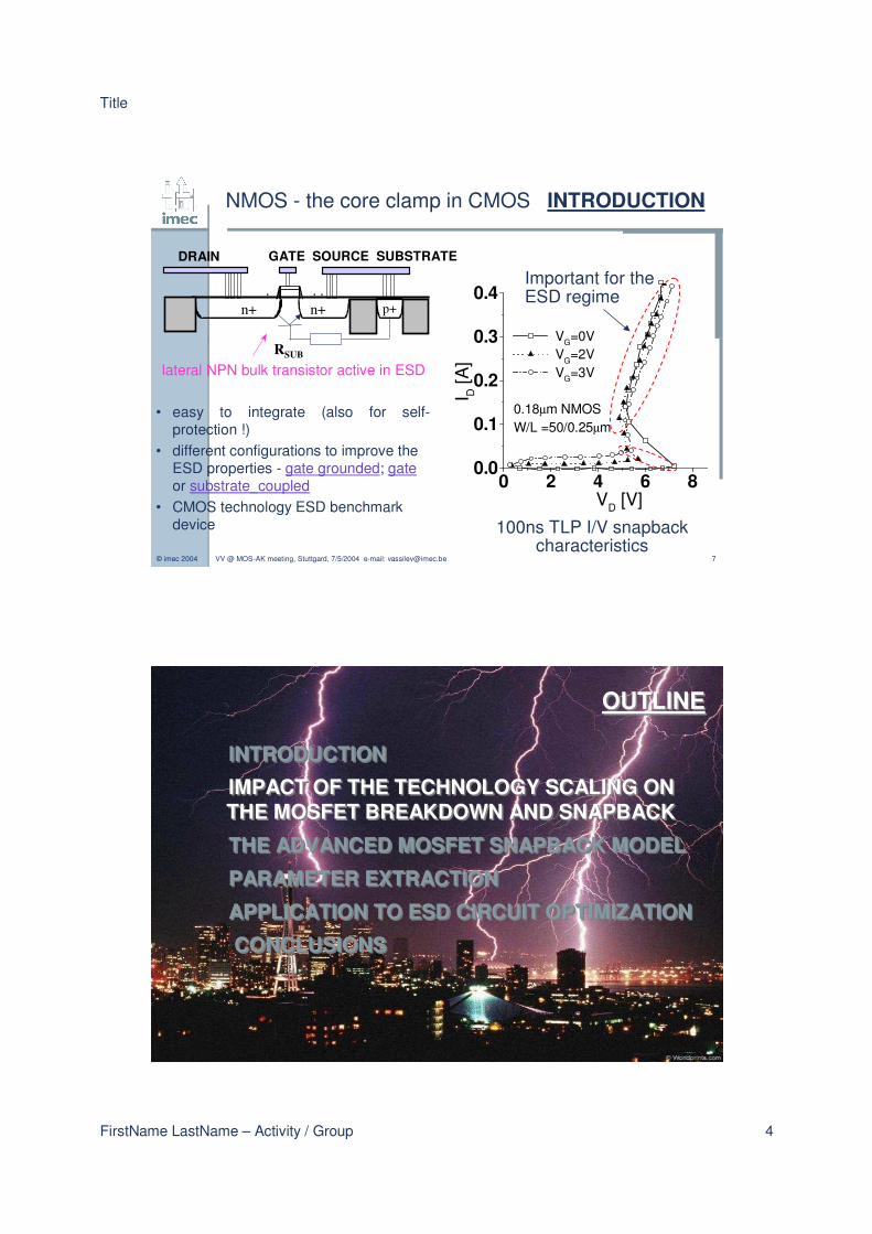
NMOS - the core clamp in CMOS INTRODUCTION
0 2 4 6 80.0
0.1
0.2
0.3
0.4
VD [V]
I D [A
]
VG=0V VG=2V VG=3V
0.18µm NMOSW/L =50/0.25µm
100ns TLP I/V snapback characteristics
lateral NPN bulk transistor active in ESD
n+ n+ p+
DRAIN GATE SOURCE SUBSTRATE
RSUB
• easy to integrate (also for self-protection !)
• different configurations to improve the ESD properties - gate grounded; gateor substrate coupled
• CMOS technology ESD benchmark device
Important for theESD regime
© imec 2004 VV @ MOS-AK meeting, Stuttgard, 7/5/2004 e-mail: [email protected] 8
OUTLINEOUTLINE
Ø INTRODUCTION
Ø IMPACT OF THE TECHNOLOGY SCALING ON THE MOSFET BREAKDOWN AND SNAPBACK
Ø THE ADVANCED MOSFET SNAPBACK MODEL
Ø PARAMETER EXTRACTION
Ø APPLICATION TO ESD CIRCUIT OPTIMIZATION
Ø CONCLUSIONS
Ø INTRODUCTION
Ø IMPACT OF THE TECHNOLOGY SCALING ON THE MOSFET BREAKDOWN AND SNAPBACK
Ø THE ADVANCED MOSFET SNAPBACK MODEL
Ø PARAMETER EXTRACTION
Ø APPLICATION TO ESD CIRCUIT OPTIMIZATION
Ø CONCLUSIONS
Title
FirstName LastName – Activity / Group 5
© imec 2004 VV @ MOS-AK meeting, Stuttgard, 7/5/2004 e-mail: [email protected] 9
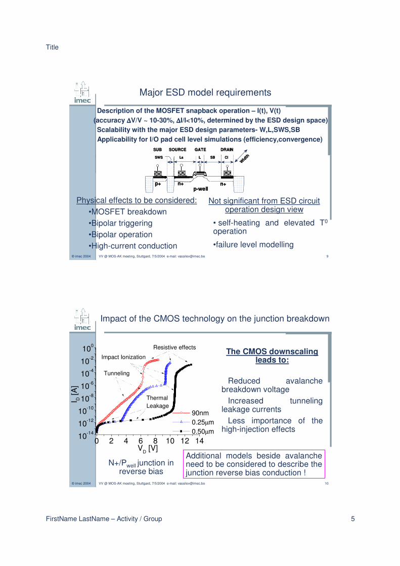
Physical effects to be considered:•MOSFET breakdown•Bipolar triggering•Bipolar operation •High-current conduction
Ø Description of the MOSFET snapback operation – I(t), V(t)(accuracy ∆∆∆∆V/V ~ 10-30%, ∆∆∆∆I/I<10%, determined by the ESD design space)
Ø Scalability with the major ESD design parameters- W,L,SWS,SBØ Applicability for I/O pad cell level simulations (efficiency,convergence)
Not significant from ESD circuit operation design view
• self-heating and elevated T0
operation
•failure level modelling
p+
L
n+n+
SOURCE DRAINGATE
p-well
SUB
SWS SBLs ClW
idth
p+
L
n+n+
SOURCE DRAINGATE
p-well
SUB
SWS SBLs ClW
idth
Major ESD model requirements
© imec 2004 VV @ MOS-AK meeting, Stuttgard, 7/5/2004 e-mail: [email protected] 10
Impact of the CMOS technology on the junction breakdown
0 2 4 6 8 10 12 1410-14
10-12
10-10
10-8
10-6
10-4
10-2
100
Thermal Leakage
Resistive effects
Tunneling
Impact Ionization
90nm 0.25µm 0.50µm
I D [A
]
VD [V]
N+/Pwell junction in reverse bias
The CMOS downscaling leads to:
üReduced avalanche breakdown voltageü Increased tunneling leakage currentsü Less importance of the high-injection effects
Additional models beside avalanche need to be considered to describe the junction reverse bias conduction !

Title
FirstName LastName – Activity / Group 6
© imec 2004 VV @ MOS-AK meeting, Stuttgard, 7/5/2004 e-mail: [email protected] 11
0 2 4 6 8 10 12 1410-15
10-13
10-11
10-9
10-7
10-5
10-3
10-1∆VBR? ∆VBR VBR
0.5µm CMOS
0.25µmCMOS
90nm CMOS
solid symbols : non-gated N+/PWell lateral diodeopen symbols : NMOS @ VG=0 (ggNMOS) device
I C/D
[A]
VC/D [V]
The breakdown of the NMOS (i.e. gated N+/Pwelljunction) is becomingincreasingly dependant on the gate field !
N+/Pwell junction in reverse breakdown
Impact of the CMOS technology on the junction breakdown behaviour: effects of the drain-gate field
© imec 2004 VV @ MOS-AK meeting, Stuttgard, 7/5/2004 e-mail: [email protected] 12
-1 0 1 2 3 4 5 6
4
5
6
7
8
9
symbols: dataline: model
90nm device
250nm device
∆V/ V ~10%
fit B
fit A
2VB
RM
OS-V
BR
diod
e [V]
VG [V]
Modeling the breakdown voltage dependence on the gate bias is needed to describe the observed ESD behaviour of
the MOSFET
� �� � � ���� ������ � � � �
•at low VGD (I.e. high drain-gate vertical field)
•at high |VGD| (I.e. low drain-gate vertical field)
� �� � � ���� ����� ������ � �� � �
� ��
��
�
�
����� � �
��� ������ �
�� � �
����� �
� �
� �� �
� ��
�
� �� �
� �� �� �� �
�
�
using the empirical model
Impact of the CMOS technology on the junction breakdown behaviour: effects of the drain-gate field

Title
FirstName LastName – Activity / Group 7
© imec 2004 VV @ MOS-AK meeting, Stuttgard, 7/5/2004 e-mail: [email protected] 13
OUTLINEOUTLINE
Ø INTRODUCTION
Ø IMPACT OF THE TECHNOLOGY SCALING ON THE MOSFET BREAKDOWN AND SNAPBACK
Ø THE ADVANCED MOSFET SNAPBACK MODEL
Ø PARAMETER EXTRACTION
Ø APPLICATION TO ESD CIRCUIT OPTIMIZATION
Ø CONCLUSIONS
Ø INTRODUCTION
Ø IMPACT OF THE TECHNOLOGY SCALING ON THE MOSFET BREAKDOWN AND SNAPBACK
Ø THE ADVANCED MOSFET SNAPBACK MODEL
Ø PARAMETER EXTRACTION
Ø APPLICATION TO ESD CIRCUIT OPTIMIZATION
Ø CONCLUSIONS
© imec 2004 VV @ MOS-AK meeting, Stuttgard, 7/5/2004 e-mail: [email protected] 14
ESD model topology and basic equations
IC
ICHID
Iavc
IDG
ISUB
RBI
RE
VRSUB
IS
DS
B
G
Iavch
CE
Bi
Iave Iavch
RCIE
ISG üEquivalent circuit model (to ease the practical implementation) üAnalog HDL implementation of the equation defined current/potential generation sources üSymmetrical topology for D/S (Important for variable polarity ESD stress e.g. CDM)üCapacitance model-the same as for the the intrinsic MOSFET
Accurate description of the actual physics and the observed ESD behaviour can be achieved
VG=0..4 V
VD [V]
I [m
A]
ITOTAL
IBJT
ICHANNELVG=0..4 V
VD [V]
I [m
A]
ITOTAL
IBJT
ICHANNEL

Title
FirstName LastName – Activity / Group 8
© imec 2004 VV @ MOS-AK meeting, Stuttgard, 7/5/2004 e-mail: [email protected] 15
ESD model topology and basic equations
Current generation sources Avalanche multiplication factors(modified Miller expressions)
•VCBi,VDBi – calculated by the model•VDsat – from the channel current model•VBR
MOS = VD @ Em=Ecritii – a semi-
empirical model that is function of VG, extracted from the measurements •km, n – extracted , cvds,cvsat-fitted
Ic, Ich- self-consistently calculatedIgen = IBTBT+ITAT – generated by the high field tunneling currents
� � ��
� � ��
�� � � ����
��� �� ��
� � � � �
� � �
� �
�
�
���
� ��
� �
�
���� �� � � �
� �� �� �� �� �� ��
�
�� �
������
�
�
����� �������� � �� � � � �
�
�
�
���
� ��
� �
�
���� �� � � �
� �� �� �� �� �� ��
�
�� �
������
�
�
����� �������� � �� � � � �
�
�
�� ��
� �
� ���� ��� �� ��� �
� ������� ���� �
� ��� ���� ��� �� ��� ���� ���
� �
� � ��� ��� �
� �� � ��
� �
� � �� �� �� �� �� �� �� �� � � �� � � �
� � �� �� �� �� �� �� �� �� �� � � �
© imec 2004 VV @ MOS-AK meeting, Stuttgard, 7/5/2004 e-mail: [email protected] 16
Typical comparison with experiments
0 2 4 6 8 10 120
20m
40m
60m
80m
100m
VG=0V MEASUREMENT VG=1V MEASUREMENT VG=2V MEASUREMENT VG=3V MEASUREMENT VG=4V MEASUREMENT COMPACT SIMULATION
I D [A
]
VD [V]
10n 100n02468
10
measured simulated with base transit time=0ns simulated with base transit time=5.5ns (LG=1.2µm)
∆Vpeak
VD ID
VD [V
]
time [s]0.00.20.40.60.81.01.2
I D [A
]
100n 200n 300n 400n 500n 600n02468
10VHBM=120V
VD [V
]
time [s]
measured simulated
Quasistatic snapback I/VESD time domain operation-
Human Body Model ESD stress

Title
FirstName LastName – Activity / Group 9
© imec 2004 VV @ MOS-AK meeting, Stuttgard, 7/5/2004 e-mail: [email protected] 17
Analog Artist/CADENCE INTEGRATION
TLP 200mA
•implementation in the standard CADENCE PDK environment•SPECTRE&HSPICE simulation
voltage waveforms current waveforms
© imec 2004 VV @ MOS-AK meeting, Stuttgard, 7/5/2004 e-mail: [email protected] 18
OUTLINEOUTLINE
Ø INTRODUCTION
Ø IMPACT OF THE TECHNOLOGY SCALING ON THE MOSFET BREAKDOWN AND SNAPBACK
Ø THE ADVANCED MOSFET SNAPBACK MODEL
Ø PARAMETER EXTRACTION
Ø APPLICATION TO ESD CIRCUIT OPTIMIZATION
Ø CONCLUSIONS
Ø INTRODUCTION
Ø IMPACT OF THE TECHNOLOGY SCALING ON THE MOSFET BREAKDOWN AND SNAPBACK
Ø THE ADVANCED MOSFET SNAPBACK MODEL
Ø PARAMETER EXTRACTION
Ø APPLICATION TO ESD CIRCUIT OPTIMIZATION
Ø CONCLUSIONS

Title
FirstName LastName – Activity / Group 10
© imec 2004 VV @ MOS-AK meeting, Stuttgard, 7/5/2004 e-mail: [email protected] 19
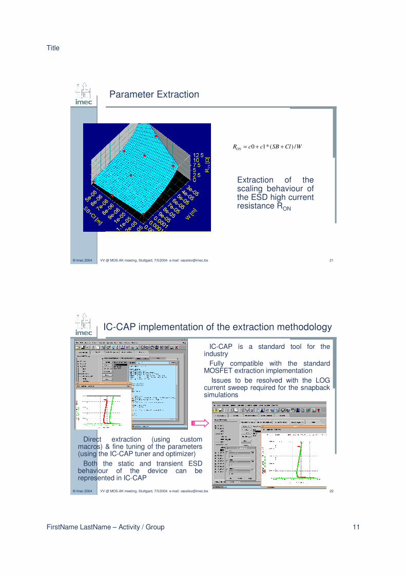
Parameter Extraction
Ø The intrinsic MOSFET – a library modelØExtraction of the bipolar parameters as function of the ESD layout variables
-multiplication factors Mb,Mch
-substrate potential and tunneling sources-current gain β-high current ‘on’ resistance-base transit time
ØScaling of the parameters - based on physically based semi-empirical expressions
IC
ICHID
Iavc
IDG
ISUB
RBI
RE
VRSUB
IS
DS
B
G
Iavch
CE
Bi
Iave Iavch
RCIE
ISG
p+
L
n+n+
SOURCE DRAINGATE
p-well
SUB
SWS SBLs ClW
idth
p+
L
n+n+
SOURCE DRAINGATE
p-well
SUB
SWS SBLs ClW
idth
The ESD model parameters are extracted from an array of structures using reverse solutions of the model equations (whenever possible) and applied to representative parts of the experimental characteristics.
© imec 2004 VV @ MOS-AK meeting, Stuttgard, 7/5/2004 e-mail: [email protected] 20
Parameter Extraction
0 2 4 6 8 1010 -15
10 -13
10 -11
10 -9
10 -7
10 -5
10 -3
10 -1
90nm deviceVBR
(2)
(1)
ID=ISUB
ID=IGD
M: km=1, n=2
ITAT: A1=8.89 10-11
B1=4.78 10-7/2
IBTBT: A2v=1.05 10-8
B2v=5.03 107
ICMEAS n+/Pw diode
ITAT(Em
lat) extracted
Mb.ITAT(Emlat) simulated
IDMEAS @ VG=0 (ggNMOS)
IBTBT (Em
vert) extracted ISUB=Mb.(IBTBT+ ITAT)
I D [A
]
VD [V]0 2 4 6 8 10 12
10 -15
10 -13
10 -11
10 -9
10 -7
10 -5
10 -3
10 -1
250nm device
ID=ISUB
VBR
IBTBT(Emlateral )
A2l=6.62 104
B2l=9.01
Mb: km=1, n=2
IBTBT(Emvert )
A2v=1.19 10-10
B2v=9.41 107
(2) (1)
ICMEAS n+/Pw diode
IBTBT(Emlat) extracted
Mb.IBTBT(Emlat) simulated
IDMEAS @VG=0 (ggNMOS)
IBTBT(Emvert) extracted
Mb.(IBTBT(Emlat)+IBTBT(Em
vert)) simulated
I D [A
]
VD [V]
Illustration of the 2-step self-consistent extraction of the breakdown and substrate tunneling currents models (the resistive behaviour model after breakdown and the high-current conduction are extracted separately)
Symbols:measurementSolid lines:extraction/simulation
Title
FirstName LastName – Activity / Group 11
© imec 2004 VV @ MOS-AK meeting, Stuttgard, 7/5/2004 e-mail: [email protected] 21
voltage waveforms current waveforms
Parameter Extraction
Extraction of the scaling behaviour of the ESD high current resistance RON
0 1*( ) /ONR c c SB Cl W= + +
© imec 2004 VV @ MOS-AK meeting, Stuttgard, 7/5/2004 e-mail: [email protected] 22
IC-CAP implementation of the extraction methodology
ØDirect extraction (using custom macros) & fine tuning of the parameters (using the IC-CAP tuner and optimizer)ØBoth the static and transient ESD behaviour of the device can be represented in IC-CAP
ü IC-CAP is a standard tool for the industryü Fully compatible with the standard MOSFET extraction implementation ü Issues to be resolved with the LOG current sweep required for the snapback simulations

Title
FirstName LastName – Activity / Group 12
© imec 2004 VV @ MOS-AK meeting, Stuttgard, 7/5/2004 e-mail: [email protected] 23
OUTLINEOUTLINE
Ø INTRODUCTION
Ø IMPACT OF THE TECHNOLOGY SCALING ON THE MOSFET BREAKDOWN AND SNAPBACK
Ø ADVANCED MOSFET SNAPBACK MODEL
Ø PARAMETER EXTRACTION
Ø APPLICATION TO ESD CIRCUIT OPTIMIZATION
Ø CONCLUSIONS
Ø INTRODUCTION
Ø IMPACT OF THE TECHNOLOGY SCALING ON THE MOSFET BREAKDOWN AND SNAPBACK
Ø ADVANCED MOSFET SNAPBACK MODEL
Ø PARAMETER EXTRACTION
Ø APPLICATION TO ESD CIRCUIT OPTIMIZATION
Ø CONCLUSIONS
© imec 2004 VV @ MOS-AK meeting, Stuttgard, 7/5/2004 e-mail: [email protected] 24
Application Examples : Multifinger device triggering
SS
SUB
D
p+
S D
G G G G
n+SWS2
SWS1
SS
SUB
D
p+
S D
G G G G
n+SWS2
SWS1
n+ n+ p+
DRAIN GATE - SOURCE - SUBSTRATE
RW ~ SWS
n+ n+ p+
DRAIN GATE - SOURCE - SUBSTRATE
RW ~ SWS
100p 1n 10n 100n0
1
2
3
4
5
6
7
8kV 6kV
4kV
2kV
8kV
4kV
2kV
6kV
VP
AD [V
]
time [s]0.0
0.5
1.0
1.5
2.0
2.5
3.0
3.5HBM stress
I ES
D [A
]
Due to the different substrate resistance of the multifinger NMOS, finger non-uniform ESD conductance can be established,which has to be avoided in the protection design
solid symbols: innermost fingers; open symbols: outermost fingers
Title
FirstName LastName – Activity / Group 13
© imec 2004 VV @ MOS-AK meeting, Stuttgard, 7/5/2004 e-mail: [email protected] 25
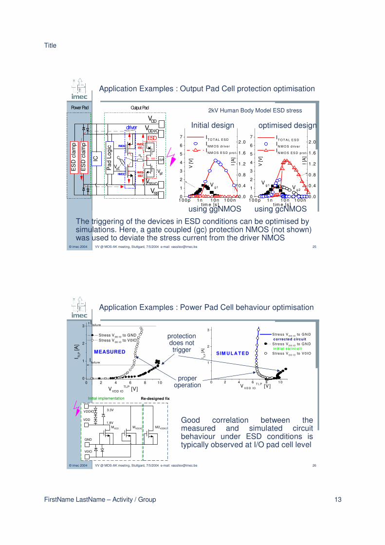
Application Examples : Output Pad Cell protection optimisation
VDD
VSS
NMOS
ESD
OUT
PMOS
Pad
Log
ic
VDD I/O
VSS I/O
ES
D c
lam
p
ES
D c
lam
p
Power Pad Output Pad
Cdg
driver
Vg1Vg2
Riso
NMOSESD
PMOSESD
IC
100p 1n 10n 100n0
1
2
3
4
5
6
7
V [V
]
t im e [s ]
0 .0
0 .4
0 .8
1 .2
1 .6
2 .0
V g1
IT O T A L E SD IN M O S d r ive r IN M O S E S D p ro t
I [A
]
100 p 1n 10 n 100n0
1
2
3
4
5
6
7
V g1 V g2
V [V
]
t im e [s ]
0 .0
0 .4
0 .8
1 .2
1 .6
2 .0 IT O T A L E S D IN M O S d rive r IN M O S ES D p ro t
I [A
]
2kV Human Body Model ESD stress
using ggNMOS using gcNMOS
The triggering of the devices in ESD conditions can be optimised by simulations. Here, a gate coupled (gc) protection NMOS (not shown) was used to deviate the stress current from the driver NMOS
Initial design optimised design
© imec 2004 VV @ MOS-AK meeting, Stuttgard, 7/5/2004 e-mail: [email protected] 26
Application Examples : Power Pad Cell behaviour optimisation
0 2 4 6 8 100
1
2
3
MEASURED
Ifailure
Ifailure
Stress VDD IO to GND Stress VDD IO to V0IO
I TLP [A
]
VVDD IOTLP [V]
MVDD MVDDIO
VDDIO
VDD
GND
V0IO
M2VDDIO
Initial implementation
3.3V
1.8V
Re-designed fix
0 2 4 6 8 10
1
2
3
S IM U L A T E D
S tress V D D IO to G N D correc ted c ircuit
S tress V D D IO to G N D initial sic ircuit
S tress V D D IO to V 0 IO
I TLP [A
]
V V D D IOT L P [V ]
Good correlation between the measured and simulated circuit behaviour under ESD conditions is typically observed at I/O pad cell level
protection does not trigger
proper operation

Title
FirstName LastName – Activity / Group 14
© imec 2004 VV @ MOS-AK meeting, Stuttgard, 7/5/2004 e-mail: [email protected] 27
OUTLINEOUTLINE
Ø INTRODUCTION
Ø IMPACT OF THE TECHNOLOGY SCALING ON THE MOSFET BREAKDOWN AND SNAPBACK
Ø ADVANCED MOSFET SNAPBACK MODEL
Ø PARAMETER EXTRACTION
Ø APPLICATION TO ESD CIRCUIT OPTIMIZATION
Ø CONCLUSIONS
Ø INTRODUCTION
Ø IMPACT OF THE TECHNOLOGY SCALING ON THE MOSFET BREAKDOWN AND SNAPBACK
Ø ADVANCED MOSFET SNAPBACK MODEL
Ø PARAMETER EXTRACTION
Ø APPLICATION TO ESD CIRCUIT OPTIMIZATION
Ø CONCLUSIONS
© imec 2004 VV @ MOS-AK meeting, Stuttgard, 7/5/2004 e-mail: [email protected] 28
CONCLUSIONS
ü EMPLOYING A GOOD CAD BASED ESD DESIGN METHODOLOGY ALLOWS TO UNDERSTAND AND OPTIMISE THE DEVICE AND CIRCUIT BEHAVIOUR IN A FASTER AND MUCH MORE RELIABLE APPROACH, NOT USING ANY BLACK MAGIC
ü THE EXTENSION OF THE STANDARD LIBRARY MOSFET MODELS TO MODELS VALID UNDER ESD STRESS WAS SHOWN TO BE POSSIBLE AND WAS VERIFIED FOR CMOS TECHNOLOGY DEVICES RANGING FROM 0.5µµµµm down to 90nm
ü THE MOSFET OPERATION UNDER ESD STRESS REQUIRES TO CONSIDER SOME SPECIFIC PHYSICAL EFFECTS
Title
FirstName LastName – Activity / Group 15
© imec 2004 VV @ MOS-AK meeting, Stuttgard, 7/5/2004 e-mail: [email protected] 29
Guido GroesenekenPhilippe JansenNatarajan MahadevaSteven ThjisTom Daenen
In a company close to you…
Acknowledgments: Acknowledgments:
�����������
Worldwide collaboration with more than 450 companies and institutes.
IMEC – Kapeldreef 75 – B-3001 Leuven – Belgium – Tel. +32 16 281211 – Fax +32 16 229400 – www.imec.be


![AN OBATA TYPE RESULT FOR THE FIRST …vassilev/CRLichObata.pdf2 S. IVANOV AND D. VASSILEV 1. Introduction The classical theorems of Lichnerowicz [29] and Obata [33] give correspondingly](https://static.fdocuments.net/doc/165x107/5f1062037e708231d448d66e/an-obata-type-result-for-the-first-vassilev-2-s-ivanov-and-d-vassilev-1-introduction.jpg)


