
MoOx back contact for CdS/CdTe thin film solar cells: Preparation, device characteristics, and...
7
MoO x back contact for CdS/CdTe thin film solar cells: Preparation, device characteristics, and stability Hao Lin a , Irfan b , Wei Xia a , Hsiang N. Wu a , Yongli Gao b , Ching W. Tang a,b,n a Department of Chemical Engineering, University of Rochester, NY 14627, United States b Department of Physics and Astronomy, University of Rochester, NY 14627, United States article info Article history: Received 9 September 2011 Received in revised form 20 December 2011 Accepted 2 January 2012 Keywords: CdTe solar cells MoO x Ohmic contact Stability abstract A novel MoO x back contact buffer has been successfully developed for thin-film CdS/CdTe solar cells. To achieve a good ohmic contact, water rinse step is necessary in order to remove surface residues from the CdTe surface prior to MoO x deposition by thermal evaporation. With MoO x as the high work function buffer, various metals can be used as the electrode to realize an ohmic back contact to p–CdTe. Thermal and light soaking stability of CdTe cells is also improved with the MoO x buffer acting as a diffusion barrier to minimize the interaction between the metal electrode and CdTe. The best performance is obtained with MoO x /Ni as the back contact for the CdS/CdTe solar cell. & 2012 Elsevier B.V. All rights reserved. 1. Introduction CdS/CdTe thin-film photovoltaic technology plays a key role in today’s fast growing photovoltaic industry, having achieved module efficiency reportedly as high as 11.7% and substantial cost reduction in manufacturing to $0.75/peak Watt [1]. The record CdS/CdTe cell efficiency remained 16.5% [2] for a decade, which was recently reported to be improved to 17.3% [1]. Although higher efficiency can be expected from bandgap consideration alone, the practical diffi- culty lies in obtaining sufficiently high p-doped CdTe [3,4]. In addition, it is difficult to realize ohmic contact to p–CdTe partly because it has a high work function of 5.7 eV, which is higher than that of most common metals. So far, the most efficient CdTe cells were produced with Cu-containing back contacts, including the use of Cu x Te [2]. However, the stability of Cu-containing contacts remained a critical issue due to Cu diffusion [5]. To address the stability issues, Cu-free back contact buffers including Sb 2 Te 3 [6] and ZnTe [7, 8] for p–CdTe have been investigated in several studies. However, the problems of inferior cell performances or contact instability associated with these Cu-free contacts have not been sufficiently understood or optimized. In this study, we have explored a new type of Cu-free contact to p–CdTe based on transitional metal oxides, which are well known for their application as high work function contacts in the field of organic electronics. In organic solar cells [9] and organic light emitting diodes [10], transition metal oxides including molybdenum oxide, nickel oxide, tungsten oxide, and vanadium oxide have been utilized as anode buffer layers to enhance the ohmic contact between indium-tin oxide (ITO) and organic layers. In particular, molyb- denum oxide (MoO x ) has been reported to have extraordinarily high work function (^ s ¼ 6.80–6.86 eV) and can be readily pre- pared by vapor deposition [11,12]. Our previous study has shown that MoO x is useful as a low-resistance back contact buffer to p– CdTe in place of the solution etching treatment method [13]. In this paper, our work on further optimization of MoO x contacts will be described, including the effects of pre- and post- MoO x deposition treatments on the cell efficiency and stability. 2. Experimental Superstrate n-CdS/p-CdTe solar cells were fabricated using previously reported procedures [14]. Briefly, 100 nm CdS films were first deposited on fluorine-doped tin oxide (FTO) substrates (Pilkington, TEC 15) using a chemical bath deposition (CBD) method [15]. CdTe films with 4 mm thickness were then deposited on the CdS films by the close-space sublimation (CSS) method [16]. The CSS deposition temperatures were 550 1C and 640 1C for the substrate and the source, respectively. The deposi- tion ambient was 1.5 Torr O 2 . The typical deposition rate under these conditions was 1 mm/min. Subsequently, a vapor cad- mium chloride (VCC) treatment was applied to the CdS/CdTe stacked films. This treatment was also carried out in a CSS setup Contents lists available at SciVerse ScienceDirect journal homepage: www.elsevier.com/locate/solmat Solar Energy Materials & Solar Cells 0927-0248/$ - see front matter & 2012 Elsevier B.V. All rights reserved. doi:10.1016/j.solmat.2012.01.001 n Corresponding author at: Department of Chemical Engineering, University of Rochester, NY 14627, United States. Tel.: þ1 585 2753552; fax: þ1 585 2733237. E-mail address: [email protected] (C.W. Tang). Solar Energy Materials & Solar Cells 99 (2012) 349–355
Transcript of MoOx back contact for CdS/CdTe thin film solar cells: Preparation, device characteristics, and...

Solar Energy Materials & Solar Cells 99 (2012) 349–355
Contents lists available at SciVerse ScienceDirect
Solar Energy Materials & Solar Cells
0927-02
doi:10.1
n Corr
Rochest
E-m
journal homepage: www.elsevier.com/locate/solmat
MoOx back contact for CdS/CdTe thin film solar cells: Preparation, devicecharacteristics, and stability
Hao Lin a, Irfan b, Wei Xia a, Hsiang N. Wu a, Yongli Gao b, Ching W. Tang a,b,n
a Department of Chemical Engineering, University of Rochester, NY 14627, United Statesb Department of Physics and Astronomy, University of Rochester, NY 14627, United States
a r t i c l e i n f o
Article history:
Received 9 September 2011
Received in revised form
20 December 2011
Accepted 2 January 2012
Keywords:
CdTe solar cells
MoOx
Ohmic contact
Stability
48/$ - see front matter & 2012 Elsevier B.V. A
016/j.solmat.2012.01.001
esponding author at: Department of Chemic
er, NY 14627, United States. Tel.: þ1 585 275
ail address: [email protected] (C.W. T
a b s t r a c t
A novel MoOx back contact buffer has been successfully developed for thin-film CdS/CdTe solar cells. To
achieve a good ohmic contact, water rinse step is necessary in order to remove surface residues from
the CdTe surface prior to MoOx deposition by thermal evaporation. With MoOx as the high work
function buffer, various metals can be used as the electrode to realize an ohmic back contact to p–CdTe.
Thermal and light soaking stability of CdTe cells is also improved with the MoOx buffer acting as a
diffusion barrier to minimize the interaction between the metal electrode and CdTe. The best
performance is obtained with MoOx/Ni as the back contact for the CdS/CdTe solar cell.
& 2012 Elsevier B.V. All rights reserved.
1. Introduction
CdS/CdTe thin-film photovoltaic technology plays a key role intoday’s fast growing photovoltaic industry, having achieved moduleefficiency reportedly as high as 11.7% and substantial cost reductionin manufacturing to $0.75/peak Watt [1]. The record CdS/CdTe cellefficiency remained 16.5% [2] for a decade, which was recentlyreported to be improved to 17.3% [1]. Although higher efficiency canbe expected from bandgap consideration alone, the practical diffi-culty lies in obtaining sufficiently high p-doped CdTe [3,4]. Inaddition, it is difficult to realize ohmic contact to p–CdTe partlybecause it has a high work function of 5.7 eV, which is higher thanthat of most common metals. So far, the most efficient CdTe cellswere produced with Cu-containing back contacts, including the useof CuxTe [2]. However, the stability of Cu-containing contactsremained a critical issue due to Cu diffusion [5]. To address thestability issues, Cu-free back contact buffers including Sb2Te3 [6] andZnTe [7,8] for p–CdTe have been investigated in several studies.However, the problems of inferior cell performances or contactinstability associated with these Cu-free contacts have not beensufficiently understood or optimized. In this study, we have exploreda new type of Cu-free contact to p–CdTe based on transitional metaloxides, which are well known for their application as high workfunction contacts in the field of organic electronics.
ll rights reserved.
al Engineering, University of
3552; fax: þ1 585 2733237.
ang).
In organic solar cells [9] and organic light emitting diodes [10],transition metal oxides including molybdenum oxide, nickeloxide, tungsten oxide, and vanadium oxide have been utilizedas anode buffer layers to enhance the ohmic contact betweenindium-tin oxide (ITO) and organic layers. In particular, molyb-denum oxide (MoOx) has been reported to have extraordinarilyhigh work function (^s¼6.80–6.86 eV) and can be readily pre-pared by vapor deposition [11,12]. Our previous study has shownthat MoOx is useful as a low-resistance back contact buffer to p–CdTe in place of the solution etching treatment method [13]. Inthis paper, our work on further optimization of MoOx contactswill be described, including the effects of pre- and post- MoOx
deposition treatments on the cell efficiency and stability.
2. Experimental
Superstrate n-CdS/p-CdTe solar cells were fabricated usingpreviously reported procedures [14]. Briefly, �100 nm CdS filmswere first deposited on fluorine-doped tin oxide (FTO) substrates(Pilkington, TEC 15) using a chemical bath deposition (CBD)method [15]. CdTe films with �4 mm thickness were thendeposited on the CdS films by the close-space sublimation (CSS)method [16]. The CSS deposition temperatures were 550 1C and640 1C for the substrate and the source, respectively. The deposi-tion ambient was 1.5 Torr O2. The typical deposition rate underthese conditions was �1 mm/min. Subsequently, a vapor cad-mium chloride (VCC) treatment was applied to the CdS/CdTestacked films. This treatment was also carried out in a CSS setup

-500
-20
0
20
40
J (m
A/c
m2 )
V (mV)
With water rinseWithout water rinse
0 500 1000
Fig. 1. J–V characteristics of CdTe cells with and without water rinse after VCC
treatment.
194
Inte
nsity
(a.u
.)
Binding energy (eV)
With water rinseWithout water rinse
Cl 2p
196 198 200 202 204 206
Fig. 2. XPS spectra of the Cl 2p core levels for CdTe surface with and without
water rinse after VCC treatment.
H. Lin et al. / Solar Energy Materials & Solar Cells 99 (2012) 349–355350
at 400 1C for both substrate and source. The treatment ambientwas 10 Torr O2 and 40 Torr N2. The treatment duration was4–6 min.
After the VCC treatment, the CdTe films were thoroughlyrinsed under a deionized water flow for several minutes and thendried under a nitrogen flow. As a back contact buffer layer, a40 nm MoOx film was thermally evaporated from MoO3 powder(Alfa Aesar, 99.95%) onto the CdTe films at a deposition rate of�5.0 A/s in a vacuum of 1�10�5 Torr, followed by the depositionof a 200 nm metal electrode by DC sputtering in 5 mTorr Arambient under 100 W power. The applied metals included Ni, Mo,Cr, Al, and Mg, and the deposition rates were 7.4, 10.8, 6.3, 6.3,and 25.0 A/s, respectively. Optional MoOx buffers were sputteredfrom a MoO3 target in an ambient of 3.0 mTorr Ar. The depositionrate for MoOx in Ar was 3.3 A/s under a power of 50 W. The activearea of the CdTe solar cell, typically about 0.1 cm2, was isolated byscribing the CdS/CdTe/MoOx/metal stack layers with a razor blade.
Thermal annealing and light soaking tests were applied to cellswith MoOx buffers. Thermal annealing was carried out at 200 1C ina tube furnace under a vacuum of �40 mTorr. Light soaking wascarried out in a custom-made light box with compact fluores-cence lamps with a light intensity of approximately 1 kW/m2. Theequilibrium temperature during the test was around 44 1C.
The current-voltage (J–V) data were obtained using a Keithleysourcemeter (Model 2400) and a tungsten-lamp-based solar simu-lator (Solux 3SS4736 50 W solar simulator). The solar simulator wascalibrated with a silicon photodiode (Hamamatsu S1787–12). Theincident light intensity on the solar cell was 80 mW/cm2. The valuesof the current density were corrected by integrating the photo-response of the cells with AM 1.5 solar spectrum.
X-ray photoemission spectroscopy (XPS) measurements werecarried out with a Surface Science Laboratories’ SSX-100, equippedwith a monochromatic Al anode x-ray gun (Ka 1486.6 eV). The basepressure of the system is 9�10�11 Torr. The spot size of the x-raywas chosen to be 1 mm in diameter and the resolution selected forenergy analyzer was 0.5 eV.
Cadmium concentrations in the rinsing solution were deter-mined using a Perkin-Elmer AAnalyst 600 atomic absorptionspectrophotometer equipped with longitudinal Zeeman back-ground correction and a transverse heated graphite furnace(Perkin-Elmer Life and Analytical Sciences). A Perkin-Elmer Cdelectrodeless discharge lamp (EDL) was the light emission source.The cadmium concentrations of the samples were obtained byregression analysis from cadmium standards with concentrationsranging from 1 to 10 ng/mL.
3. Results and discussion
3.1. CdTe surface cleaning process
In this study, we found that surface cleaning can critically affectthe cells fabricated with vapor-deposited MoOx as the back contactbuffer. First, we examined the effect of water rinse. After VCCtreatment, the CdTe film was rinsed in deionized water and thendried under N2 flow prior to the deposition of MoOx/Ni back contact.A control cell without water rinse was also prepared. J–V character-istics are shown in Fig. 1. With water rinse, normal J–V characteristicsand device performance (Z¼12.4%, Jsc¼21.4 mA/cm2, Voc¼813 mV,FF¼71.4%) are obtained for the cell. In contrast, a severe roll-over inthe forward bias direction is observed in the control cell. This roll-over behavior results in substantially inferior device performance(Z¼7.9%, Jsc¼21.3 mA/cm2, Voc¼783 mV, FF¼47.4%).
As a standard device fabrication process, VCC treatment iscommonly carried out in an oxygen containing atmosphere atelevated temperatures [17]. This process is known to produce
residues, identified as Cd3Cl2O2 and Te6O11Cl2 on the CdTe surfacein one study [18]. We have used different methods to removesurface residues produced by VCC treatment, including thermaldesorption in vacuum and solvent rinse. We also explored VCCtreatment in an oxygen-free atmosphere with the hope of redu-cing the residue formation. So far, water rinse appears to be mosteffective in removing the residues. We have examined thechemical composition of the CdTe surface with XPS. A key findingis that water-soluble and chlorine-containing compounds arepresent on the CdTe surface after subjecting CdTe to VCC treat-ment. As shown in Fig. 2, for the CdTe film without water rinse,the XPS spectrum shows a strong Cl 2p peak with a bindingenergy of 198.7 eV. With water rinse, Cl 2p peak is undetectable.In addition, we have determined the Cd content in the chlorine-containing compound through atomic absorption analysis. Weinfer from the analysis that the residue contains Cd3Cl2O2 or amixed composition of CdCl2 and CdO. The thickness of this layer isabout 0.9–2.5 A. The fact that the residue cannot be removed bythermal desorption in vacuum is consistent with the knownthermal stability of Cd3Cl2O2, which is non-volatile up to 600 1C[18]. The existence of a thin layer of Cd3Cl2O2 is a plausible causefor the reduction of the work function of MoOx and consequently
0.4
0.6
0.8
1.0
Thermal evaporationSputteringA
bsor
banc
e
H. Lin et al. / Solar Energy Materials & Solar Cells 99 (2012) 349–355 351
the roll-over behaviors observed in the cells without water rinseprior to the back contact formation.
The work function of MoOx is highly sensitive to surfacecontamination. For instance, air exposure of MoOx after MoOx
deposition reduced the work function from 6.80 eV to 5.24 eV[12]. In our research, we found that the ohmicity of CdTe/MoOx islargely controlled by the deposition of the first few monolayers ofMoOx on the CdTe surface. The existence of a thin layer of residuemay substantially compensate the work function of MoOx, whichwe suggest is the reason for the roll-over in Fig. 1.
3.2. MoOx deposition methods
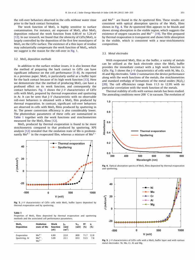
In addition to the surface residue issues, it is also known thatthe method of preparing the back contact to CdTe can havesignificant influence on the cell performance [5–8]. As reportedin a previous paper, MoOx is particularly useful as a buffer layerfor the back contact because of its high work function [13]. Herewe demonstrate that the method of producing MoOx can have aprofound effect on its work function, and consequently thecontact behaviors. Fig. 3 shows the J–V characteristics of CdTecells with MoOx prepared by thermal evaporation and sputteringin Ar. It can be seen that J–V characteristic with no observableroll-over behaviors is obtained with a MoOx film produced bythermal evaporation. In contrast, significant roll-over behaviorsare observed in cells with MoOx films produced by sputtering inAr. The power conversion efficiency is also considerably lower.The photovoltaic parameters of these cells are summarized inTable 1 together with the work functions and stoichiometriesmeasured for the MoOx films [12].
MoOx produced by thermal evaporation is found to be morestoichiometric compared to that produced by sputtering. XPSanalysis [12] revealed that the oxidation state of Mo is predomi-nantly Mo6þ in the evaporated film, whereas a mixture of Mo5þ
-500
-20
0
20
40
J (m
A/c
m2 )
V (mV)
Thermal evaporationSputtering
0 500 1000
Fig. 3. J–V characteristics of CdTe cells with MoOx buffer layers deposited by
thermal evaporation and by sputtering.
Table 1Properties of MoOx films deposited by thermal evaporation and sputtering
methods and the associated cell performance parameters.
MoOx
DepositionOxidationstate of Mo
Workfunction(eV)
Jsc
(mA/cm2)
Voc
(mV)FF(%)
g(%)
Evaporation Mo6þ 6.80 22.0 809 71.7 12.8
Sputtering, Ar Mo6þ ,
Mo5þ
5.09 22.1 653 53.5 7.8
and Mo6þ are found in the Ar-sputtered film. These results areconsistent with optical absorption spectra of the MoOx filmsshown in Fig. 4. The Ar-sputtered film appears to be bluish andshows strong absorption in the visible region, which suggests theexistence of oxygen vacancies and Mo5þ [19]. The film preparedby thermal evaporation is transparent and shows little absorptionin the visible, which is consistent with a near-stoichiometriccomposition.
3.3. Metal electrodes
With evaporated MoOx film as the buffer, a variety of metalscan be utilized as the back electrode since the MoOx bufferprovides the immediate contact with a high work function toCdTe. Fig. 5 shows the J–V characteristics of cells with Ni, Mo, Cr,Al and Mg electrodes. Table 2 summarizes the device performancealong with the work functions of the metals, the stoichiometriesand standard enthalpy of formations of the metal oxides (MxOy)[20]. The cell efficiencies range from 11.5 to 12.9% with noparticular correlation with the work function of the metals.
Thermal stability of cells with various metals has been studied.The annealing conditions were 200 1C in vacuum. The evolution of
3000.0
0.2
Wavelength (nm)400 500 600 700 800
Fig. 4. Optical absorption spectra of MoOx films deposited by thermal evaporation
and sputtering.
-500
-20
0
20
40NiMoCrAlMg
J (m
A/c
m2 )
V (mV)0 500 1000
Fig. 5. J–V characteristics of CdTe cells with a MoOx buffer layer and with various
metal electrodes: Ni, Mo, Cr, Al and Mg.

H. Lin et al. / Solar Energy Materials & Solar Cells 99 (2012) 349–355352
the cell performance parameters is plotted in Fig. 6. The changesin the cell efficiency and series resistance after an annealingduration of 19.0 hr are summarized in Table 3. Regardless of themetal electrode, the rate of cell degradation appears to be thefastest in the first 4.5 hr, after which the rate is almost zero. Thecells with Ni and Mo electrodes are the most stable, with a
Table 2Properties of metals applied to CdTe/MoOx films and the associated
function (Fm), possible metal oxides (MxOy) and standard enthalpy
Metal Um (eV) MxOy: Standard enthalpyof formation (kJ/mol)
Ni 5.04–5.35 Ni2O3: �489.5
Mo 4.36–4.95 MoO3: �745.1
Cr 4.5 Cr2O3: �1139.7
Al 4.06–4.26 Al2O3: �1675.7
Mg 3.66
0
5
10
Ni Mo Cr Al
Annealing duration (hr)
η (%
)
400
600
800
Ni Mo Cr Al
Annealing duration (hr)
Voc
(mV)
0 5 10 15 20
0 5 10 15 20
Fig. 6. Evolution of cell performance parameters during the thermal annealing test: (a
factor.
decrease in efficiency of 13.5% and 16.9%, respectively. In contrast,the cell with Al electrode is the least stable, showing a degrada-tion of 63.2% in efficiency along with a large increase in the seriesresistance. In all cases, the cell degradation is associated with thedevelopment of the roll-over behaviors. The J–V curves of thesecells are shown in Fig. 7.
device performance parameters. The properties include work
of formation of the metal oxides.
Jsc
(mA/cm2)Voc
(mV)FF(%)
g(%)
22.0 808 72.6 12.9
21.9 817 68.1 12.2
22.0 805 65.0 11.5
22.3 815 68.4 12.4
21.7 811 71.9 12.7
5
10
15
20
25
Ni Mo Cr Al
Jsc
(mA
/cm
2 )
Annealing duration (hr)
020
40
60
Ni Mo Cr Al
Annealing duration (hr)
FF (%
)
5 10 15 20
0 5 10 15 20
) efficiency, (b) short-circuit current density, (c) open-circuit voltage, and (d) fill

H. Lin et al. / Solar Energy Materials & Solar Cells 99 (2012) 349–355 353
The development of roll-over behaviors can be attributed tothe reactivity of the back contact metal with the MoOx buffer.Such a reaction will result in the partial reduction of MoOx and alowering of its work function. Therefore the effectiveness of theMoOx as a high work function is compromised. The severeinstability associated with the Al back contact can be related toits large standard enthalpy of formation of Al2O3 (�1675.7 kJ/mol)compared to that of MoO3 (�745.1 kJ/mol), favoring the abstrac-tion of oxygen from MoOx in contact with Al. As a result, the cellwith Al shows much stronger roll-over behavior compared to theother metals. The cells with Ni and Mo are most stable, which is
Table 3Efficiencies (Z) and series resistance (Rs) for cells before and after thermal
annealing test.
Ni Mo Cr Al
Z Before annealing (%) 12.6 12.4 11.3 12.5
After annealing (%) 10.9 10.3 7.8 4.6
Change (%) �13.5 �16.9 �31.0 �63.2
Rs Before annealing (O cm2) 4.5 4.7 7.3 4.8
After annealing (O cm2) 9.1 9.5 16.3 129.7
Change (%) þ102.2 þ102.1 þ123.3 þ2602.1
-20
0
20
40
Before annealing After annealing
-20
0
20
40
V (mV)
Before annealing After annealing
J (m
A/c
m2 )
J (m
A/c
m2 )
-500 0 500 1000
V (mV)-500 0 500 1000
Fig. 7. J–V characteristics for cells before and after thermal annealing tests. The con
consistent with their much lower standard enthalpy of formationof their oxides.
3.4. Light soaking test
Light soaking experiments were carried out on CdTe cells withMoOx as the buffer layer and Ni as the back electrode. The cellwithout MoOx buffer was used as the control. Both cells weresubjected to light soaking under open circuit for a duration of 395days in laboratory ambient at an average temperature of 44 1C.The evolution of the cell performance parameters is shown inFig. 8. Although both cells suffer overall efficiency degradation,the cell with the MoOx buffer shows improved stability (with anefficiency decrease by 16.9%) over the cell without the buffer(with an efficiency decrease by 23.9%), indicating that MoOx
buffer is effective in slowing the cell degradation induced by Nidiffusion during light soaking [21].
4. Conclusions
We have found that the CdS/CdTe thin film solar cell isimproved by using MoOx as the back contact buffer layer. Toachieve an ohmic contact, however, it is necessary to remove
-20
0
20
40
J (m
A/c
m2 )
Before annealing After annealing
-500
-20
0
20
40
J (m
A/c
m2 )
V (mV)
Before annealing After annealing
0 500 1000
-500V (mV)
0 500 1000
tact electrodes for each cell in the figures are: (a) Ni, (b) Mo, (c) Cr, and (d) Al.

0
5
10
MoOx/Ni
Ni
η (%
)
5
10
15
20
25
MoOx/Ni
Ni
Jsc
(mA
/cm
2 )
500
600
700
800
Light soaking duration (day)
MoOx/Ni
Ni
Voc
(mV)
040
50
60
70
Light soaking duration (day)
MoOx/Ni
Ni
FF (%
)
100 200 300 4000 100 200 300 400
Light soaking duration (day)0
Light soaking duration (day)100 200 300 4000 100 200 300 400
Fig. 8. Evolution of cell performance parameters during the light soaking test: (a) efficiency, (b) short-circuit current density, (c) open-circuit voltage, and (d) fill factor.
H. Lin et al. / Solar Energy Materials & Solar Cells 99 (2012) 349–355354
surface residues from the CdTe surface and use thermal evapora-tion for the deposition of MoOx film. With MoOx as the backcontact buffer, various metals with different work functions canbe used as the back contact electrode to achieve relatively highefficiencies. However, significant differences in degradation withthermal annealing were observed. Cells with high work functionmetals including Ni and Mo as the back electrode show betterstability compared to those with low work function metals suchas Al. Light soaking tests show that the stability of the cell is alsoenhanced with MoOx as the back contact buffer.
Acknowledgments
This work was partially supported by Rohm and Haas Com-pany. HL thanks Bob Gelein for the AA characterization andDr. David Weiss for discussion on the manuscripts.
References
[1] First Solar Inc. website at: /http://www.firstsolar.com/S.[2] X. Wu, J.C. Keane, R.G. Dhere, C. DeHart, D.S. Albin, A. Duda, T.A. Gessert,
S. Asher, D.H. Levi, P. Sheldon, 16.5%-Efficient CdS/CdTe polycrystalline thin-film solar cell, in: Proceedings of the 17th IEEE European Photovoltaic SolarEnergy Conference, Munich, Germany, 2001, pp. 995–1000.
[3] J. Sites, J. Pan, Strategies to increase CdTe solar-cell voltage, Thin Solid Films
515 (2007) 6099–6102.[4] A.L. Fahrenbruch, Exploring back contact technology to increase CdS/CdTe
solar cell efficiency, in: Materials Research Society Symposium Proceedings
1012, 2007, pp. 283–290.[5] K.D. Dobson, I. Visoly-Fisher, G. Hodes, D. Cahen, Stability of CdTe/CdS thin-
film solar cells, Solar Energy Materials and Solar Cells 62 (2000) 295–325.[6] D.L. Batzner, A. Romeo, M. Terheggen, M. Dobeli, H. Zogg, A.N. Tiwari, Stability
aspects in CdTe/CdS solar cells, Thin Solid Films 451–452 (2004) 536–543.[7] A.D. Compaan, A. Gupta, J. Drayton, S.H. Lee, S. Wang, 14% sputtered thin-film
solar cells based on CdTe, Physica Status Solidi B-Basic Research 241 (2004)
779–782.[8] D. Rioux, D.W. Niles, H. Hochst, ZnTe—A potential interlayer to form low-
resistance back contacts in CdS/CdTe solar cells, Journal of Applied Physics 73
(1993) 8381–8385.[9] M.D. Irwin, B. Buchholz, A.W. Hains, R.P.H. Chang, T.J. Marks, p-Type
semiconducting nickel oxide as an efficiency-enhancing anode interfacial
layer in polymer bulk-heterojunction solar cells, Proceedings of the National
Academy of Sciences of the United States of America 105 (2008) 2783–2787.[10] H. You, Y.F. Dai, Z.Q. Zhang, D.G. Ma, Improved performances of organic light-
emitting diodes with metal oxide as anode buffer, Journal of Applied Physics
101 (2007) 026105/1–026105/3.[11] M. Kroger, S. Hamwi, J. Meyer, T. Riedl, W. Kowalsky, A. Kahn, Role of the
deep-lying electronic states of MoO3 in the enhancement of hole-injection in
organic thin films, Applied Physics Letters 95 (2009) 123301/1–123301/3.[12] M.L. Zhang, Irfan, H.J. Ding, Y.L. Gao, C.W. Tang, Organic Schottky barrier
photovoltaic cells based on MoOx/C60, Applied Physics Letters 96 (2010)
183301/1–183301/3.[13] H. Lin, W. Xia, H.N. Wu, C.W. Tang, CdS/CdTe solar cells with MoOx as back
contact buffers, Applied Physics Letters 97 (2010) 123504/1–123504/3.

H. Lin et al. / Solar Energy Materials & Solar Cells 99 (2012) 349–355 355
[14] W. Xia, J.A. Welt, H. Lin, H.N. Wu, M.H. Ho, C.W. Tang, Fabricationof Cd1�xZnxS films with controllable zinc doping using a vapor zincchloride treatment, Solar Energy Materials and Solar Cells 94 (2010)2113–2118.
[15] T.L. Chu, S.S. Chu, N. Schultz, C. Wang, C.Q. Wu, Solution-grown cadmium-sulfide films for photovoltaci devices, Journal of Electrochemical Society 139(1992) 2443–2446.
[16] N. Romeo, A. Bosio, A. Romeo, An innovative process suitable to producehigh-efficiency CdTe/CdS thin-film modules, Solar Energy Materials and SolarCells 94 (2010) 2–7.
[17] B.E. McCandless, K.D. Dobson, Processing options for CdTe thin film solarcells, Solar Energy 77 (2004) 839–856.
[18] D.M. Waters, D. Niles, T.A. Gessert, D. Albin, D.H. Rose, P. Sheldon, Surfaceanalysis of CdTe after various pre-contact treatments, in: Proceedings of theSecond IEEE World Conference and Exhibition on Photovoltaic Solar EnergyConversion, Vienna, Austria, 1998, pp. 1043–1046.
[19] V.K. Sabhapathi, O.M. Hussain, P.S. Reddy, K.T.R. Reddy, S. Uthanna,B.S. Naidu, P.J. Reddy, Optical-absorption studies in molybdenum trioxidethin-films, Physica Status Solidi a-Applied Research 148 (1995) 167–173.
[20] W.M. ‘‘Mickey’’ Haynes, Handbook of Chemistry and Physics Online, 91stEdition, Taylor and Francis Group, 2010–2011.
[21] S.H. Demtsu, D.S. Albin, J.W. Pankow, A. Davies, Stability study of CdS/CdTesolar cells made with Ag and Ni back-contacts, Solar Energy Materials andSolar Cells 90 (2006) 2934–2943.


![2< ' # '9& *#: & ; · QDs (e.g., CdTe-CdS and CdTe-ZnS QDs) were achieved via organic synthesis [3e,f]. It is worth noting that, these orQDs cannot be directly used in bioapplications](https://static.fdocuments.net/doc/165x107/5f4c449da14099768c22651d/2-9-qds-eg-cdte-cds-and-cdte-zns-qds-were-achieved.jpg)


![High-efficiency CdTe/CdS core-shell nanocrystals in water ... · Semiconductor quantum dots (QDs) have found important applications including biological labeling , 2], light-emitting](https://static.fdocuments.net/doc/165x107/5f0d67d67e708231d43a319f/high-efficiency-cdtecds-core-shell-nanocrystals-in-water-semiconductor-quantum.jpg)

