Modulation Techniques for Biomedical Implanted - MDPI.com
23
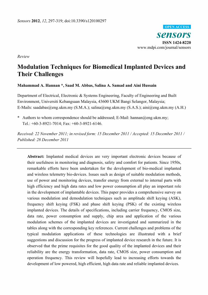
Sensors 2012, 12, 297-319; doi:10.3390/s120100297 sensors ISSN 1424-8220 www.mdpi.com/journal/sensors Review Modulation Techniques for Biomedical Implanted Devices and Their Challenges Mahammad A. Hannan *, Saad M. Abbas, Salina A. Samad and Aini Hussain Department of Electrical, Electronic & Systems Engineering, Faculty of Engineering and Built Environment, Universiti Kebangsaan Malaysia, 43600 UKM Bangi Selangor, Malaysia; E-Mails: [email protected] (S.M.A.); [email protected] (S.A.S.); [email protected] (A.H.) * Authors to whom correspondence should be addressed; E-Mail: [email protected]; Tel.: +60-3-8921-7014; Fax: +60-3-8921-6146. Received: 22 November 2011; in revised form: 15 December 2011 / Accepted: 15 December 2011 / Published: 28 December 2011 Abstract: Implanted medical devices are very important electronic devices because of their usefulness in monitoring and diagnosis, safety and comfort for patients. Since 1950s, remarkable efforts have been undertaken for the development of bio-medical implanted and wireless telemetry bio-devices. Issues such as design of suitable modulation methods, use of power and monitoring devices, transfer energy from external to internal parts with high efficiency and high data rates and low power consumption all play an important role in the development of implantable devices. This paper provides a comprehensive survey on various modulation and demodulation techniques such as amplitude shift keying (ASK), frequency shift keying (FSK) and phase shift keying (PSK) of the existing wireless implanted devices. The details of specifications, including carrier frequency, CMOS size, data rate, power consumption and supply, chip area and application of the various modulation schemes of the implanted devices are investigated and summarized in the tables along with the corresponding key references. Current challenges and problems of the typical modulation applications of these technologies are illustrated with a brief suggestions and discussion for the progress of implanted device research in the future. It is observed that the prime requisites for the good quality of the implanted devices and their reliability are the energy transformation, data rate, CMOS size, power consumption and operation frequency. This review will hopefully lead to increasing efforts towards the development of low powered, high efficient, high data rate and reliable implanted devices. OPEN ACCESS
Transcript of Modulation Techniques for Biomedical Implanted - MDPI.com
Sensors 2012, 12, 297-319; doi:10.3390/s120100297
sensors ISSN 1424-8220
www.mdpi.com/journal/sensors
Review
Modulation Techniques for Biomedical Implanted Devices and Their Challenges
Mahammad A. Hannan *, Saad M. Abbas, Salina A. Samad and Aini Hussain
Department of Electrical, Electronic & Systems Engineering, Faculty of Engineering and Built
Environment, Universiti Kebangsaan Malaysia, 43600 UKM Bangi Selangor, Malaysia;
E-Mails: [email protected] (S.M.A.); [email protected] (S.A.S.); [email protected] (A.H.)
* Authors to whom correspondence should be addressed; E-Mail: [email protected];
Tel.: +60-3-8921-7014; Fax: +60-3-8921-6146.
Received: 22 November 2011; in revised form: 15 December 2011 / Accepted: 15 December 2011 /
Published: 28 December 2011
Abstract: Implanted medical devices are very important electronic devices because of
their usefulness in monitoring and diagnosis, safety and comfort for patients. Since 1950s,
remarkable efforts have been undertaken for the development of bio-medical implanted
and wireless telemetry bio-devices. Issues such as design of suitable modulation methods,
use of power and monitoring devices, transfer energy from external to internal parts with
high efficiency and high data rates and low power consumption all play an important role
in the development of implantable devices. This paper provides a comprehensive survey on
various modulation and demodulation techniques such as amplitude shift keying (ASK),
frequency shift keying (FSK) and phase shift keying (PSK) of the existing wireless
implanted devices. The details of specifications, including carrier frequency, CMOS size,
data rate, power consumption and supply, chip area and application of the various
modulation schemes of the implanted devices are investigated and summarized in the
tables along with the corresponding key references. Current challenges and problems of the
typical modulation applications of these technologies are illustrated with a brief
suggestions and discussion for the progress of implanted device research in the future. It is
observed that the prime requisites for the good quality of the implanted devices and their
reliability are the energy transformation, data rate, CMOS size, power consumption and
operation frequency. This review will hopefully lead to increasing efforts towards the
development of low powered, high efficient, high data rate and reliable implanted devices.
OPEN ACCESS
Sensors 2012, 12
298
Keywords: modulation techniques; bio-medical/wireless implanted devices; power
amplifiers; inductive coupling link
1. Introduction
Biomedical implantable devices have been available for more than sixty years. The first transistorized
biomedical implanted device was designed and developed by Earl Bakken in 1957 for the cardiac
pacemaker [1]. Investigations on implanted devices have been focused of the most important issues of
biomedical implants, which are patient safety and comfort [2]. This can be achieved by reducing the
power consumption and ensuring efficient energy transfer to the implanted devices [3]. Therefore,
wireless energy transfer is an important issue for implanted devices [4].
Implanted medical devices are electronic devices that monitor and diagnose the electromyography
(EMG), electrocardiogram (ECG), electroretiuogram (ERG) and electrooculography (EOG) of the
patient and send current to various parts of a patient body. In general, the implanted device consists of
two parts: the internal part located underneath the body skin and an external part. i.e., controller [5,6].
The external part is used for powering the combination and sending data to the outside world.
Implantable devices are self-operating devices which adjust their operation depending upon the
patient’s condition. These devices do not rely on external sources of power. Thus, low power
consumption and high data rate are the main requirements for medical implant devices [7]. In order to
minimize cost, patient trauma and risk associated with the repeated surgeries, it is necessary to increase
the lifetime of implanted batteries by conserving energy at every stage of a device’s operation. Thus, in
order to consume the power during monitoring and diagnosis, implanted devices powered by RF
signals through inductive coupling links are used to reduce the complexity of the system [8].
There are many methods to conserve power and reduce the interference on nearby electronics by
choosing the suitable modulation and suitable design of the modulator and demodulator. Details of the
modulation and demodulation of wireless telemetry and implanted devices such as amplitude shift
keying (ASK), frequency shift keying (FSK) and phase shift keying (PSK) have been discussed in
many reviews. However, still there are many drawbacks with the communication systems of the
existing designed and developed devices. There are a lot of papers in the field of wireless low power
electronics, such as optical biomedical sensing [9], cochlear implants [10] biomedical wireless sensor
networks [11], intelligent biomedical devices [12] and body sensors [13]. This paper provides a
detailed review of the literature concerning the design of low power transmitters for different forms of
digital bandpass modulations used in implanted devices covering the period from 2000 to 2011. The
purpose of this review is to discuss and classify all the types of digital modulation used in wireless
telemetry bio-devices and biomedical implanted devices to provide a good background on the
challenges and problems that are being faced and to develop appropriate solutions.
2. Systems Overview
In general, wireless telemetry bio-devices and biomedical implanted devices mainly consist of two
parts: an external one, located outside the human body and an internal part, located inside the human
Sensors 2012, 12
299
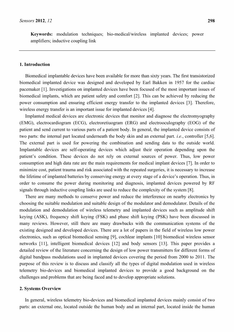
body. The external part is used to supply power and transmit the data to the internal part through an
inductive coupling link as well as monitor the data from the human body [14,15]. Details of the data
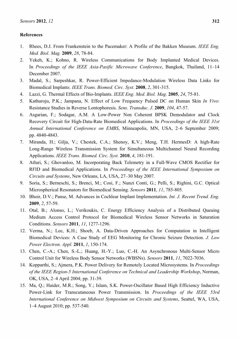
transmission between the parts are shown in Figure 1.
Figure 1. Architecture for data and power transmission system.
2.1. Power Supply Technologies
The power supply technologies used in the aforesaid devices can be classified according to the
applications of the implanted devices. Generally, the implanted devices can be powered by batteries
such as in the case of pacemakers, cochlear implants, retinal prosthesis, brain implants, etc. However,
the limited lifetime of the implanted batteries lead to many challenges to improve their longevity. The
wireless telemetry bio-devices can also be powered by radio frequency (RF) signals, transmitting
power from the external part to the internal part through an inductive coupling coil and then converted
into AC and DC voltage [16]. Another source of harvested energy is used to power the implanted devices
such as knee implants that use the vibration of piezoelectric materials [17] or body motion [18].
2.2. Wireless Communication Technologies for Implanted Devices
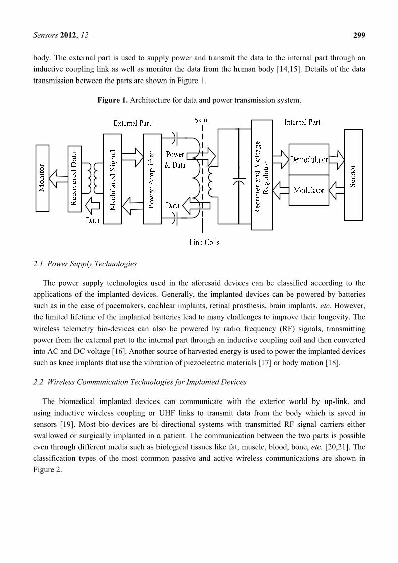
The biomedical implanted devices can communicate with the exterior world by up-link, and
using inductive wireless coupling or UHF links to transmit data from the body which is saved in
sensors [19]. Most bio-devices are bi-directional systems with transmitted RF signal carriers either
swallowed or surgically implanted in a patient. The communication between the two parts is possible
even through different media such as biological tissues like fat, muscle, blood, bone, etc. [20,21]. The
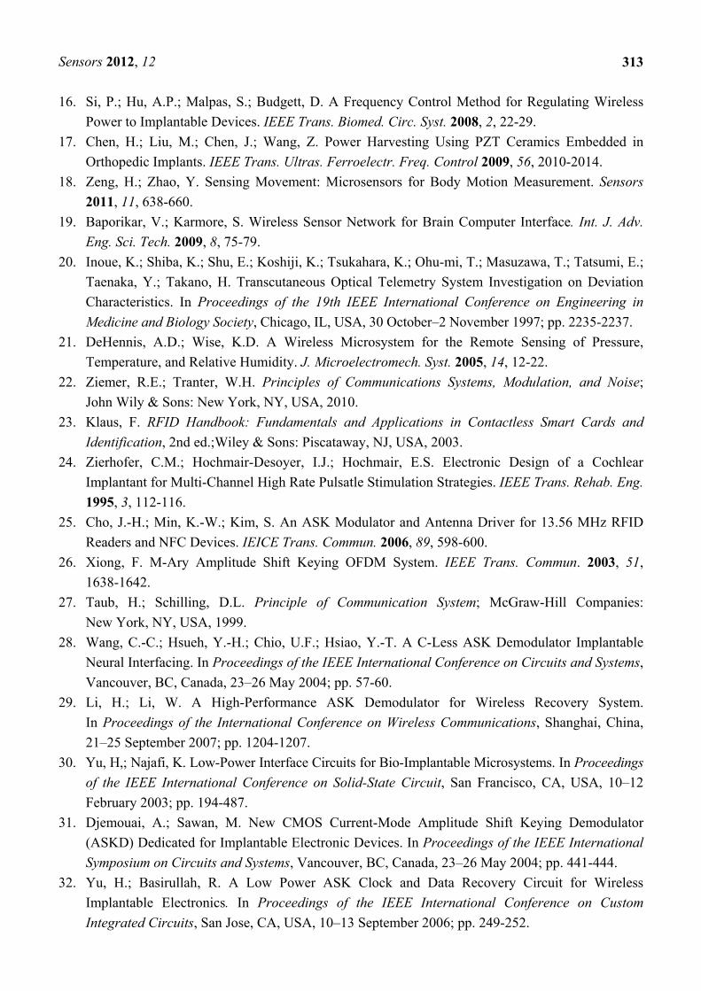
classification types of the most common passive and active wireless communications are shown in
Figure 2.
Sensors 2012, 12
300
Figure 2. Communication technologies for wireless telemetry.
2.3. Characteristics of the Implantable Devices
There are several characteristics that are shared by most biomedical implantable devices as follows:
i. Low Power Consumption: low power consumption is the main requirement for medical implant
devices where the large dissipation in power increases the possibility to damage the soft tissues
in the human body. Changing or charging batteries can be inconvenient, difficult, costly and
even risky for the patient; all implantable medical devices need to consume as little energy as
possible.
ii. High Reliability: A failure of an implantable medical device can result on inconvenience, pain,
damage or even death for the patient. Maintenance is also costly and risky. Thus, reliability for
the implanted devices must be very high.
iii. Low Voltage Signals: Most of the natural signals are inside the human bodies as well as the
output of the transducers are in the V or mV range, which requires special care in sensing and
amplifying.
iv. Low Frequencies: The natural frequency span of biological signals varies from a fraction
of a hertz to several kilohertz, However, most of the implantable devices are powered by
low-frequency (<1 MHz signal) magnetically coupled coils (often modulated to include the
data telemetry). Nowadays, the designers design the bio-implanted devices to operate in the
medical implant communications service (MICS) band.
v. Small Size: Implantable devices need to be as small as possible, so as to be less invasive to the
human body. This does not always means that the silicon area should be as small as possible,
because increasing the silicon area to minimize external components can reduce overall size. In
addition the use of some methods such as auto-zeroing techniques, FPGA methods, and
artificial intelligence methods can help minimize the overall size.
Sensors 2012, 12
301
3. Modulation Techniques
Digital modulation techniques impress the digital signal onto a carrier signal for data transmission.
A sequence of digital data is used to alter the parameter of a high frequency called carrier signal. Thus,
signal transmission takes place by modulating different parameters like amplitude, phase and frequency
of the signal. Modulation techniques provide high data rate transmission, data security, quality signal,
simple architecture, low power consumption, good performance over a fading communication channel,
increased channel capability, greater accuracy in the presence of noise and distortion, etc. [22]. However,
there are a number of tradeoffs in the digital modulation like hard to design complex structured,
disadvantages of analog counterparts and bandwidth size. The main criteria for choosing the kind of
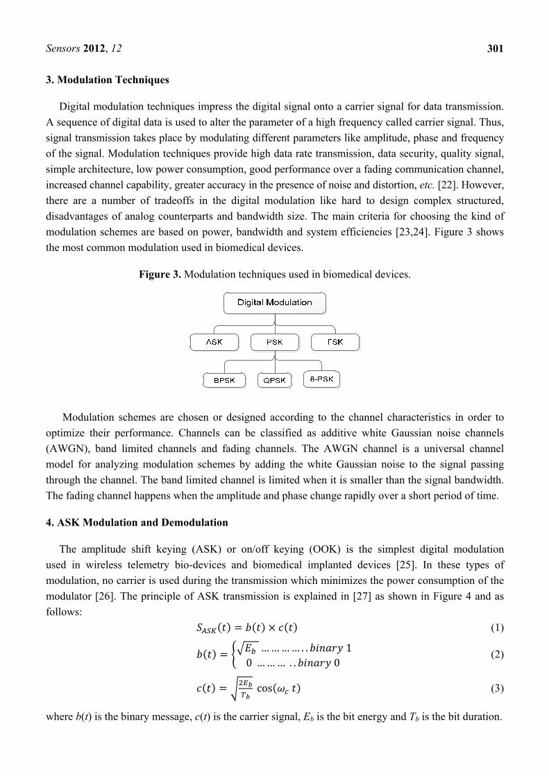
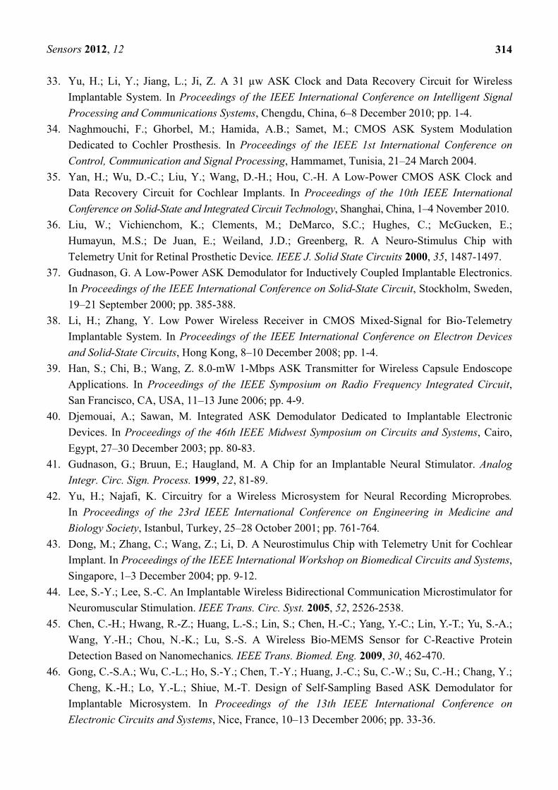
modulation schemes are based on power, bandwidth and system efficiencies [23,24]. Figure 3 shows
the most common modulation used in biomedical devices.
Figure 3. Modulation techniques used in biomedical devices.
Modulation schemes are chosen or designed according to the channel characteristics in order to
optimize their performance. Channels can be classified as additive white Gaussian noise channels
(AWGN), band limited channels and fading channels. The AWGN channel is a universal channel
model for analyzing modulation schemes by adding the white Gaussian noise to the signal passing
through the channel. The band limited channel is limited when it is smaller than the signal bandwidth.
The fading channel happens when the amplitude and phase change rapidly over a short period of time.
4. ASK Modulation and Demodulation
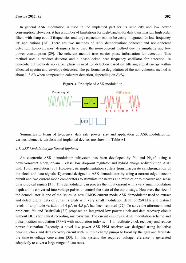
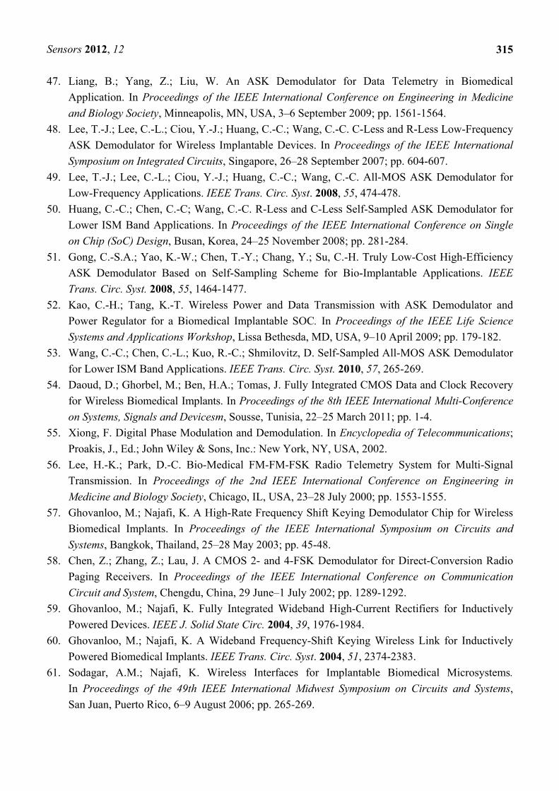
The amplitude shift keying (ASK) or on/off keying (OOK) is the simplest digital modulation
used in wireless telemetry bio-devices and biomedical implanted devices [25]. In these types of
modulation, no carrier is used during the transmission which minimizes the power consumption of the
modulator [26]. The principle of ASK transmission is explained in [27] as shown in Figure 4 and as
follows:
(1) … … … … . . 10 … … … . . 0 (2)
cos (3)
where b(t) is the binary message, c(t) is the carrier signal, Eb is the bit energy and Tb is the bit duration.
Sensors 2012, 12
302
In general ASK modulation is used in the implanted part for its simplicity and low power
consumption. However, it has a number of limitations for high-bandwidth data transmission, high order
filters with sharp cut off frequencies and large capacitors cannot be easily integrated for low-frequency
RF applications [28]. There are two methods of ASK demodulation: coherent and non-coherent
detection, however, most designers have used the non-coherent method due its simplicity and low
power consumption [29]. The coherent method uses carrier phase information for detection. This
method uses a product detector and a phase-locked beat frequency oscillator for detection. In
non-coherent methods no carrier phase is used for detection based on filtering signal energy within
allocated spectra and envelope detectors. The performance degradation of the non-coherent method is
about 1–3 dB when compared to coherent detection, depending on Eb/N0.
Figure 4. Principle of ASK modulation.
Summaries in terms of frequency, data rate, power, size and application of ASK modulator for
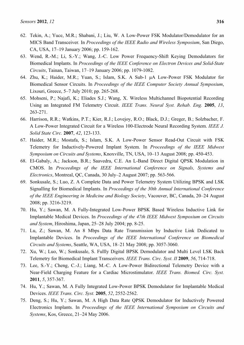
various telemetric wireless and implanted devices are shown in Table A1.
4.1. ASK Modulation for Neural Implants
An electronic ASK demodulator subsystem has been developed by Yu and Najafi using a
power-on-reset block, op/am E class, low drop-out regulator and hybrid charge redistribution ADC
with 10-bit resolution [30]. However, its implementation suffers from inaccurate synchronization of
the clock and data signals. Djemouai designed a ASK demodulator by using a current edge detector
circuit and two current mode comparators to stimulate the nerves and muscles or to measure and sense
physiological signals [31]. This demodulator can process the input current with a very smal modulation
depth and is converted into voltage pulses to control the state of the ouput stage. However, the size of
the demodulator is one of the issues. A new CMOS current mode ASK demodulator used to extract
and detect digital data of current signals with very small modulation depth of 250 kHz and distinct
levels of amplitude variation of 4 μA to 4.5 μA has been reported [22]. To solve the aforementioned
problems, Yu and Basirullah [32] proposed an integrated low power clock and data recovery circuit
without DLLs for neural recording microsystem. The circuit employs a ASK modulation scheme and
pulse position modulation (PPM) with modulation index m = 1 to facilitate clock recovery and reduce
power dissipation. Recently, a novel low power ASK-PPM receiver was designed using inductive
peaking, clock and data recovery circuit with multiple charge pumps to boost up the gain and facilitate
the time-to-voltage conversion [33]. In this system, the required voltage reference is generated
adaptively to cover a large range of data rates.
Sensors 2012, 12
303
4.2. ASK Modulation for Cochlear Implants
The electronic system of the modulator and demodulator is replaced by a NAND gate, diode and RC with CMOS transistor to control the carrier signal for cochlear prostheses [34]. This system used five inverters in order to satisfy the constraint of integration and to generate an oscillation operated carrier frequency of 20 MHz. Recently, Yan et al. [35] proposed a monostable circuit for low-power CMOS ASK system with clock and data recovery for cochlear implants integrated under 0.18 µm CMOS technology. Pulse width modulation (PWM) signals with delay-locked loops (DLL) are used to recover and resynchronize the clock and data of the system [36]. However, the expense of increased area and overhead power are problems in this system.
4.3. ASK Modulation for Complex Implants
Gunnar tested an ASK modulator with 200 Kbps carrier frequency to achieve high small-signal bandwidth with low power levels and this unit worked better for complex implants such as stimulating electrode arrays or visual implants [37]. A high performance and low power consumption unit without capacitor and resistor and with clock recovery circuit of 10 MHz carrier frequency, 0.35 µm CMOS, 2 Mbps data rate and less than 84 µw ASK demodulator was developed for complex implants [29]. The wireless receiver of the ASK demodulator consisted of a current source, a class AB operational amplifiers with common source, a track and latch stage and a Schmitt trigger. To reduce the CMOS size, Li and Zhang [38] developed a novel mixed-signal interface for bio-telemetry complex implantable systemd consisting of a digital processing circuit and analog front-end. The system included power amplifier, ASK demodulator, clock extraction and power recovery without passive elements, i.e., capacitor and resistor. The CMOS size is reduced to 0.18 µm, which is less than that of other complex implant systems and in addition, the power supply is only 1.8 V.
4.4. ASK Modulation for Wireless Telemetry and Endoscopic Implants
In wireless capsule endoscopic systems, the data transmission from inside to outside the human body is high to achieve high quality medical images, so for quality internal biomedical imaging, Han et al. [39] proposed a pseudo differential stacked class-A power amplifier based on phase lock loop (PLL) and RF conversion circuit. In the system, a 20 MHz, 0.25 µm CMOS, 1 Mbps data rate, 3.62 mm2 chip area of 3.17 mA power consumption ASK modulator is used to generate the low frequency carrier by a voltage controlled oscillator and convert the low frequency ASK signal into the 2.4 GHz industrial scientific and medical (ISM) band. However, the sizes of the demodulators are still not up to the level needed. Therefore, after a detailed review of the demodulators like CMOS current mode [40], wireless capsule endoscopic application [39], neuro-stimulus chip for retinal prosthetics, neuromuscular, cochlear devices [36,41-44] and nano-mechanics based C-reactive protein detection [45], Gong et al. [46] proposed a self-sampling demodulator without passive elements consisting of a pulse shaper, voltage scalar, level contractor and self-sampler. Again in 2009, Liang et al. [47] designed an ASK demodulator for wireless telemetry biomedical applications, which supports data rates up to 300 kbps and detects envelopes with a modulation index of 1% or more. The circuit design includes a single-to-differential OTA, a current mode full-wave rectifier, a log-domain peak detector, a variable-gain amplifier and a comparator.

Sensors 2012, 12
304
4.5. ASK Modulation for General Implant Applications
To reduce the size of the implanted devices, a low-efficient RF induced capacitor-less, i.e., C-less
ASK demodulator was developed to regulate the stable output voltage. The detailed characteristics
of the proposed demodulator are shown in [28]. In order to further reduce the size of implantable
devices, Lee et al. [48,49] developed C-less and R-less without trigger envelope detectors. These
demodulators improve the noise margin and also reduce the quantity of transistors. Huang et al. [50]
also designed a ASK demodulator without passive elements and with only 15 CMOS transistors. The
demodulator has a high bandwidth of 300 MHz for lower ISM band frequencies, which is enough for
almost all kinds of biomedical implantations. Gong et al. [51] developed their previous work [46]
further, providing the ability of working over a small modulation index without any passive elements
using a self- sampling scheme to reduce the chip area and cost as well as to receive higher efficiency.
Kao et al. [52] designed an ASK demodulator based on a maximum modulation index up to 2.86% and
a 50% maximum modulation rate. The size of the CMOS is comparatively smaller in this general
category of biomedical implants. The modulation index and rate are designed as: 100% (4) 100% (5)
where VH and VL represent the maximum and minimum amplitudes of the modulated signal wave form
in which the modulation index increases the efficiency of the system and reduces the size. Data rate is
the rate at which information is being transferred and operating carrier is the suitable operating
frequency in the modulation rate or signaling speeds that contributes to transfer data rate with high
efficiency.
To reduce the power consumption in medical implanted devices an ASK demodulator without using
any passive elements has been designed [53]. It consists of a rectifier, an envelope detector, digital
shaper and load driver. In general, non-coherent ASK modulators are sensitive to the carrier frequency
and modulation index. To avoid this disadvantage, a new circuit based comparator is designed in an
ASK demodulator including a full wave rectifier, a voltage reference and a small capacitor to filter the
high frequency components and a signal formatter circuit [54].
5. FSK Modulation and Demodulation
FSK is one of earliest and most suitable modulation techniques for digital modulation. The principle
of FSK modulation is to send binary data with two different frequencies and the resultant modulated
signal is regarded as amplitude modulation (AM) of different carrier frequencies. There are two types
of FSK modulation: i.e., non-coherent or discontinuous and coherent FSK modulation [55]. In the
non-coherent types of FSK modulation different frequencies is represented by binary 1 and 0 as follows: cos 2 , 1 , 1 cos 2 , 1 , 0 (6)
Sensors 2012, 12
305
where ϕ1 and ϕ2 are initial phases at t = 0 and they are not the same in general. T is the bit period of
the binary data. This type can be generated by switching the modulator output line between two
different oscillators. However, in the coherent types of FSK modulation, the two coherent signals have
the same initial phase ϕ at t = 0 as follows: cos 2 , 1 , 1 cos 2 , 1 , 0 (7)
In this section, a detailed summary of FSK modulation in terms of frequency, data rate, power, sizes
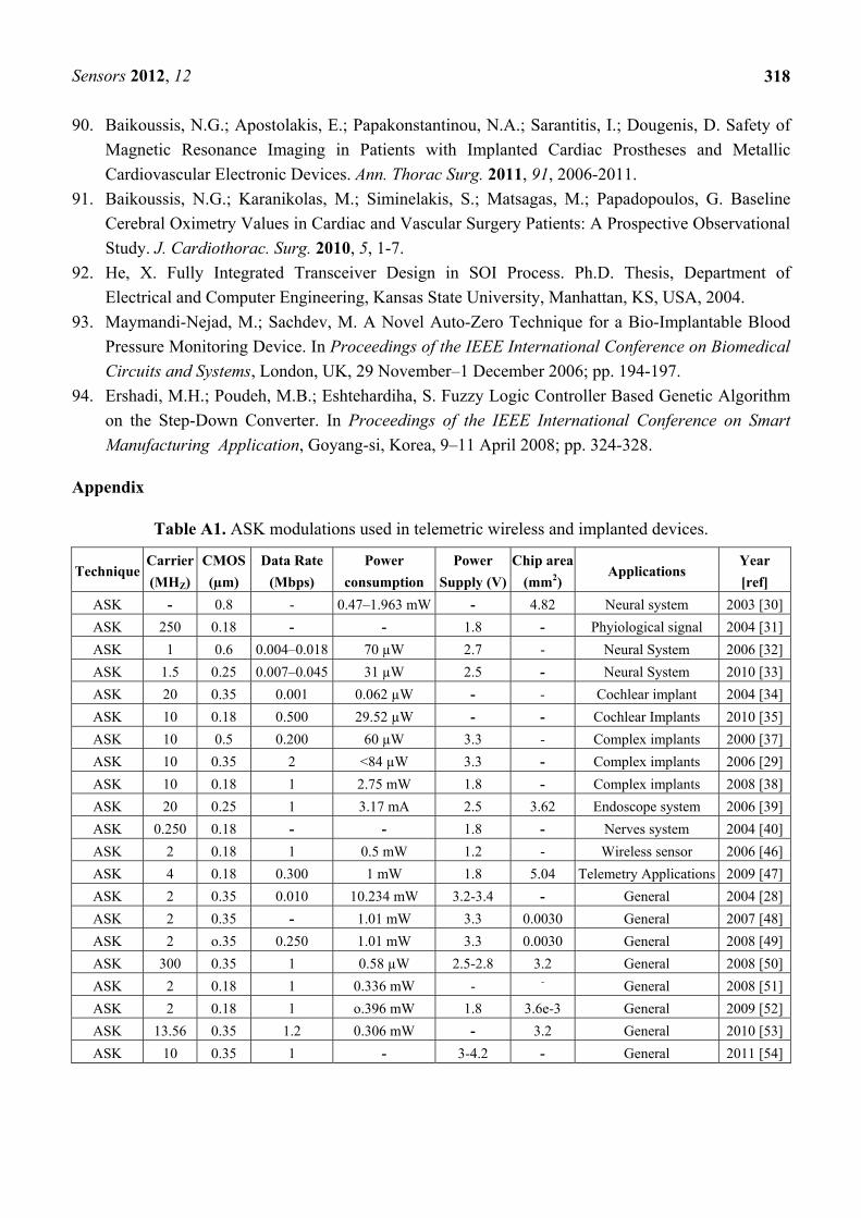
and applications of various telemetric wireless and implanted devices is listed in Table A2.
5.1. FSK Modulation for Biological Implants
It is usually necessary for a nurse to be near a patient all the time for monitoring and watching
the patient’s condition. To avoid this situation, a new kind of low cost monitoring system is
developed [56] that consists of a transmitter and receiver. The transmitter is located near the patient or
can be attached to him and the receiver located in the monitoring room to be watched and monitored
by the physician and the nurses. The multi-signal of the system is modulated by analog FM modulation
and FSK carrier frequencies at 447 MHz. However, the system suffers from interfacing between the
signals and noise. To address the above issues, a low-power FSK modulator and demodulator for
biological signals can be used to reduce the noise. The transmitter side of the system can also be used a
four stage differential ring VCO with tone frequency located at 402–405 MHz carrier frequency.
5.2. FSK Modulation for General Implants
Much research has been focused on various types of biomedical implant devices. In this regards,
Ghovanloo and Najafi [57] developed an FSK protocol and compared it with the ASK protocol. The
developed high rate data transfer protocol receives the serial bit from the input clock, extracted from
2 MHz to 20 MHz FSK carrier signal. The extracted FSK signal is as follows: sin 2 sin 2 (8)
A novel 4-FSK demodulator technique was used to improve the bit error rate (BER) performance
and to increase the decision accuracy of the system by generating additional zero-crossing using a
modified ZIFZCO with clocks [58]. However, this device has relative high power consumption.
Ghovanloo and Najafi [59] further developed this work in [57] using the same carrier frequency to
reduce the power consumption and chip area. The demodulator circuit of the system is developed with
a data rate to carrier frequency ratio up to 67% to require a much lesser power consumption of
0.38 mW. Again, Ghovanloo and Najafi [60] developed a three FSK demodulator circuit with data-rate
up to carrier-frequency ratio up to 67% in 5–10 MHz. This novel method was used to send data
inductively to a wireless biomedical implant with 4 Mbps data rates. The power consumption and the
chip area of the implanted devices are comparatively less than that of the previous system.
CMOS technology is very popular for designing an effective modulator. Accordingly, Sodagar and
and Najafi [61] reviewed many of the implanted circuits and devices that used standard CMOS
technologies. Tekin et al. [62] have developed a low power FSK modulator/demodulator for an MICS
Sensors 2012, 12
306
band transceiver to reduce the CMOS size and chip area. Wend et al. [63] developed two different
types of demodulators such as an analogue FSK (AFSK) and a digital FSK (DFSK) for general
implanted devices. The AFSK consists of a signal balance mixer and a comparator, however, the
DFSK consists of only one block. Both demodulators are implemented in 0.18 µm CMOS technology
with a power supply of 1 V. The AFSK demodulator occupies a chip area of 0.016 mm2 and the data
rate is 2.5 Mbps. The DFSK occupies a chip area of 0.004 mm2 and the data rate is up to 5 Mbps. The
power consumption of ASFK and DFSK demodulators are 0.47 mW and 0.022 mW, respectively.
5.3. FSK Modulation for Physiological Implants
To monitor the various physiological parameters inside the human body, the transmitter unit sends
the sensor data outside the human body as explained by Zhu et al. [64]. This paper proposed a new
low-power (FSK) modulator for biomedical sensors. The new circuit integrates the modulation
functionality into the oscillator itself by using the data signal to control the oscillation frequency, and
the circuit can generate a tunable carrier frequency for different data signals. The author compared his
work with another works such as Mohseni et al. [65], which provided one silicon chip which combines
single-channel and multi channel with lower dissipation. Harrison et al. [66] developed a prototype
integrated circuit for wireless neural recording from 100-channel microelectrode. Haider et al. [67]
proposed a system consisting of a FSK generator block and data generator used for low-voltage and
low-power operation. However, Zhu et al. [64] developed a FSK modulator for biomedical sensor
circuits that has better properties for physiological implants.
6. PSK Modulation and Demodulation
Phase shift keying (PSK) constitutes a large class of digital modulation techniques. In the last
decades PSK modulation has been widely used in wireless communication for biomedical modulation
techniques. This review includes the important research which has used PSK modulation in biomedical
applications. In PSK modulation, correlated or matched filter implementation of the coherent detector
are compared with a reference signal. The reference signal is generated by the carrier recovery circuit,
which is synchronous to the received signal in terms of frequency and phase. However, the differential
coherent demodulator is non-coherent in the sense that phase coherent reference signals are not
required, which is used to overcome the adversary effect of the random phase in the received signal.
The most common digital schemes appropriate for biomedical data transmission are briefly described
as PSK, binary PSK (BPSK), differential PSK (DPSK), quadrature PSK (QPSK), differential quadrature
PSK (DQPSK), offset quadrature PSK (OQPSK) and quasi-coherent PSK (QCPSK) in [68,69], as
shown in Table A3.
6.1. PSK Modulation for Various Stimulator Implants
A stimulator is an agent that excites some functional activity of the human body. Accordingly, Hu
and Sawan [70] developed a fully integrated neuromuscular stimulator with a BPSK demodulator
using COSTAS loop topology. The demodulator consists of comparator, multipliers, loop filters, VCO
and 90° phase shifter. The BPSK demodulator can be modified as a QPSK demodulator to get double
Sensors 2012, 12
307
the data transfer rate. These types of demodulators are complex in function. To reduce the complexity
of the system and to achieve low power and high data rate transmission, Lu and Sawan [71] designed a
system with two modulators and two demodulators using OQPSK modulation. The circuit was
integrated in 0.18 µm CMOS technology and operated with 13.56 MHz carrier frequency to achieve
8 Mbps data rates, i.e., very fast transmission. The power consumption of the modulators and
demodulators is relative low. The BPSK modulation was also used to transmit data and power from the
external part to the implant and the load shift keying (LSK) modulation is used to transmit the received
data from the implant to the external part [72]. The implanted device consists of a BPSK demodulator
that functions as a brain stimulator-based PLL. Lee et al. [73] proposed a bio-device for transcutaneous
wireless telemetry using the near-field inductive coupling technique with round-wire coils for a cardiac
micro stimulator. PSK modulation is used to decode the transmission data.
6.2. PSK Modulation for General Implants
To reduce the size and power consumption, Hu and Sawan [74] further developed their previous
work keeping the same parameters in [70] but using BPSK modulation for general body implants. The
BPSK demodulators in [70,71] were further developed by Deng et al. [75] using QPSK modulation
and modified COSTAS loop technology. The program was simulated using same carrier frequency of
13.56 MHz with a data rate of 4 Mbps, i.e., faster data transmission. Again, a BPSK demodulator is
designed using a phase frequency detector based PLL for robust performance [76]. Two different
circuit implementationa for demodulator with a carrier frequency of 13.56 MHz are used in this system.
6.3. PSK Modulation for Neural Implants
Most implantable devices use an inductive coupling link to transmit both power and data between
coils using the same carrier frequency. The system circuit configuration is complex. Zhou et al. [77]
separated the power and data, then transmitted them with different frequencies using DPSK modulation
employing two transmitters and two receivers. The system power is transmitted with 1 MHz carrier
frequency and the data is transmitted with 20 MHz carrier frequency. This method made the system
simpler by reducing the circuit complexity. However, the as-developed system is big in size and has
higher power consumption compared with other systems. The model of the system is as follows: 0 (9) ∞ 1 (10)
where ω1 and ω2 are frequency components of the two resonant tanks, respectively. L1 and L2 are the
inductances and C1 and C2 are the capacitances of a linearized model coupling between two resonant
tanks, respectively. K is the coupling coefficient between coils that results in frequencies splitting
away from their original values. When k ≠ 0, both resonant tanks will contain frequency components
ω1 and ω2. However, no interference is present at k = 0, i.e., the power and data resonant tanks remain
at their original frequencies. When k = 1, the upper frequency shifts to infinity. Again, when L1 >> L2
and ω1 ≈ ω2, the frequency of the power resonant tank is hardly affected due to the small amount of
interference from the data transmitter.
Sensors 2012, 12
308
A non-coherent PSK receiver without PLL was developed by using a band pass sampling theory for neural implants [78]. Zhou et al. [79] further developed his prior system [77] using a DPSK modulation in the analog domain to cancel the interference signal for a dual-band. This system is able to cancel 12 dB interferences signals without using complex filters. The system still suffered from high power consumption. In general, wireless powered signal-to-noise ratio (SNR) of the received signal is high for the short-range in neural implants. To overcome this situation, Gong et al. [80] proposed a quasi-coherent PSK (QCPSK) demodulator employing a direct carrier processing to extract the timing signals.
In order to eliminate the power interference in the data receiver in neural implants, a fully integrated DPSK is used for high density biomedical implants through dual-band telemetry [81]. The carrier frequency of the power and data rate are separated within a minimum sampling rate which results in reduced chip area and makes it possible for all blocks to be implemented in one chip. This system suffers from relatively high power consumption. Power consumption is an essential key in biomedical implantable devices. To achieve reduced power consumption, a BPSK demodulator based on a digital-analog hybrid COSTAS loop and a digital multiplier is proposed in [82]. The digital multiplier is used in place of an analog multiplier to reduce the power consumption.
6.4. PSK Modulation for Complex Implants
Complex implants are very sensitive to data transmission problems. In this regard, a new fully digital BPSK demodulator and load shift keying (LSK) has been used in complex implanted devices to reduce the power consumption and increase the data transmission rate [83]. The back telemetry technique is used in this work and verified through simulation and measurement. The obtained results show that the system improves the data transmission rate compared to conventional bi-level back telemetry. Furthermore, Xu et al. [84] improved their previous work in [83] by using a fully digital BPSK demodulator based on digital PLL and a multi level LSK modulator to generate the incoming BPSK signal data for complex implants with higher data rate back telemetry.
Retinal and cochlear complex implants require high speed data transfer. A novel BPSK data demodulator and clock recovery circuit based on noncoherence is developed in [85,86] in which the developed circuit works with the outstanding data-to-carrier-frequency ratio of 100%. The demodulator powered the implanted device with high data rate and low power consumption, as can be seen in Table A3. The demodulator is implemented in a 0.18 µm CMOS process with 10–20 MHz carrier frequency. The power consumption is only 119–310 µW with this 10–20 Mbps data rate, which are a lower power consumption and higher data rate compared to the previous work.
The analysis, investigation and experimental measurements for high data rates have been developed using FPGA/CLPC programming [87]. The n-PSK demodulator was programmed with VHDL to generate digital binary quadrature and eight PSK signals. In this system the carrier frequency was chosen to be 135 kHz operated by inductively coupled RF power and a modified hybrid class E and F power amplifier was used to simulate the system. Asgarian and Sodagar [88] proposed his further designed modulator based on QPSK using FPGA/CPLD for implantable telemetry applications. The local clock oscillator is used at 25.175 MHZ with a carrier frequency of 12.5 MHZ. This proposed design has low power consumption and is small in size, which makes it suitable for biomedical applications. To improve the high data rate transmission and reduced the system complexity, Asgarian

Sensors 2012, 12
309
and Sodagar [89] proposed a phase-silence-shift keying (PSSK) modulation. PSSK modulation needs double the bandwidth of PSK modulation.
7. Current Challenges and Problems
Biomedical device technology has been recently used for medical applications in the human body
by monitoring or recording many signals such as EMG, ECG, EOG and ERG and monitoring or
diagnosing the current conditions of implantable devices such as retinal implants, cochlear implants,
pacemakers, brain implants and for wireless capsule endoscopy. Two of the most important issues for
biomedical implants are patients’ safety and comfort. These can be achieved by reducing the power
consumption, switching losses, choosing suitable modulation and carrier frequency according to a
MICS table and by increasing the efficient energy transfer capabilities , for example, using near-field
wireless energy transfer that results in electromagnetic fields that would not heat the tissues. However,
for example, heating of pacemaker leads is the major problem undermining magnetic resonance
imaging. Therefore, hundreds of patients with a pacemaker or implantable cardioverter face safety and
reliability issues [90,91]. Typically a wireless biomedical devices consists of two parts, the external
part that transmits RF signals to the internal part through an inductive coupling downlink using variety
of modulated signals such as ASK, FSK, PSK (BPSK, QPSK, DBPSK, DQPSK, OQPSK), and it must
transmit with high efficiency and low power consumption. Thus, an aim of research into implantable
biomedical devices is to develop such devices with low power consumption, efficient energy transfer,
the highest data rate, efficient power amplifiers, small size and low-cost, so many parameters need to
be considered, as discussed in the following sections.
7.1. Adopting the Proper Method to Choose the Suitable Modulation Used for the Wireless Telemetry
Adopting aproper method to choose the suitable modulation to be used for the wireless telemetry
depends on the nature and type of the implanted device. Some implanted devices such as brain, retinal,
cochlear implants, and wireless capsule endoscopy require high data rate transmission [35,38,39].
Thus, the advantages and disadvantages of the suitable modulations used in biomedical devices and
biotelemetry systems need to be focused. For example, the BPSK modulation offers a practical circuit
implementation by transmitting 1-bit binary data by the influence of shifted carrier frequency, which
does not change the phase carrier of the sine wave. However, there is a change in the carrier phase to a
negative sine wave for 0-bit. Thus, the BPSK is only able to modulate 1-bit/symbol, which may not
provide a high enough data rate due to the bandwidth limitations and and the demodulator power
consumption [27]. These problems can be solved by techniques offering high data rates like QPSK and
n-PSK modulation. However, these suffer from complicated structures and high power consumption,
as explained in Section 6. The FSK is general uses two signals with different frequencies to represent
binary 1 and 0. These modulations offer high date rates and suffered from complications and size
issues [22,26] as explained in Section 6. The PSK and FSK are used for implanted devices which need
high data rates such as retinal and cochlear implants. We have seen that ASK modulation is more
suitable than FSK and PSK for implant devices and telemetry systems within a short range. Thus,
modulation with simple hardware implementation and small in size, fast and reliable transmission, less
power consumption and constant RF signal would be the best choice for a wireless telemetry system.
Sensors 2012, 12
310
7.2. Suitable Carrier Frequency
The carrier frequency is very important in designing implanted devices and biotelemetry systems.
Most of the implantable devices are powered by low frequency, less than 1 MHz, however, the
standard safety levels with respect to human body exposure to radio frequency electromagnetic fields
is 3 kHz–30 GHz [4]. The standards frequencies according to the MICS are specified between the
frequencies of 402–405 MHz, which involves a number of allowable frequencies such as 27 MHz. The
second standard is the ISM standard dealing with 13.56 MHz band. The RFID standard deals with
125–135 kHz for low frequency bands. The low and high frequencies between 3 kHz–30 MHz are
widely used in transcutaneous wireless due to its ability penetrate water and skin over a short range.
7.3. Suitable Power and Class Amplifier
The power amplifier plays an important role in low and high frequency bands to amplify the signal
to a certain coupling coil which transmits the power and data to the implantable devices. Thus, an
implant system needs a highly efficient power amplifier. The suitable class of amplifier is very
important to transmit a stable RF signal with high efficiency compared to these conventional
amplifiers such as class A, B, C [92]. In general, class E and F amplifiers have the same properties and
are widely used in implantable devices and telemetry systems. The E class amplifier requires only one
active device within kHz to several MHz, in which shifting resonance frequency decreases the output
power transmission. Thus, an automatic frequency correction circuit is needed for high rates of data
transmission. However, F class amplifiers require at least two active devices, which increases the
power consumption and size. The frequency is limited in low frequencies due to its switching losses.
Thus, higher frequencies and inductively coupled system are suitable for better response and
comparatively efficient even in the case of frequency shifting.
7.4. Coils Used in the Wireless Telemetry System
The wireless inductive coupling use the magnetic field to transfer data and power from the external
part to the internal part. In general, RF short-range communication transmits a low power irradiated
from the reader coil antenna to offer fixed sinusoidal carrier amplitude that provides a stable wireless
transfer power. The bio-device system is composed by a primary coil integrated and isolated inside the
human body and a secondary coil located outside the body. In most cases, the primary coil is tuned in
series resonance to provide a low impedance load for driving the transmitter coil, whereas the secondary
coil is almost invariably in parallel. Thus, to have better power transfer efficiency of inductive coupling
link both sides of the link are tuned at the same resonant frequency and the stability of the RF signal
need to provide a high readability at the implant device in terms of the distances from the reader coil.
7.5. Size of the Implanted Devices
Implantable devices need to be as small as possible, so as to be less invasive for the human body.
The batteries in biomedical implants have several problems such as limited life time, chemical side
effects and being large in size. Researchers are trying to eliminate the use of batteries from implanted
devices in the human body and have proposed various solutions to power implantable devices such as
Sensors 2012, 12
311
using inductive coupling link, power harvesting with piezoelectric material and body motion. The
silicon area should be as small as possible to minimize external components that can reduce the overall
size of implantable devices. Reducing the complexity of the electronic block circuits and the number
of the passive elements such as capacitors and resistors would help to reduce the size of the implanted
devices. This can be achieved by developing techniques and methods such as auto-zero technique [93],
FPGA methods [86] and artificial intelligence methods [94].
7.6. Low-Cost and Simplest Design
In the 1950s, when the first biomedical implantable devices was implanted, the focus was on
scientific success, and the economic aspectd were not important at that time. However, with the
increasing use of the biomedical implantable devices, the economy of the implantable devices is very
important. in addition to safety and comfort for the patient. Thus, low-cost and simple designs became
an important factor and challenges for the designers.
8. Conclusions and Suggestions
This article outlines the various modulation techniques and their suitability for wireless data
transmission for bio-medical implanted devices. The different modulation schemes show different
types of bandwidth data transmission and frequencies. The ASK modulation is based on on/off keying,
multiplication of the binary message and the carrier signal used for low power consumption, while the
FSK mode is the most suitable digital modulation, which sends binary data with two different
frequencies and the resultant modulated signal is represented by binary 1 and 0. PSK is the largest
class of digital modulation applied in complex bio-medical implanted devices by coupling inductive
link to transmit both power and data between coils using the same carrier frequency. The review
investigated and observed that the quality of the implanted devices and their reliability depends on the
modulation scheme in terms of data transmission, operating frequency and power consumption. The
main challenges in existing biomedical devices are the data transfer rated, suitable modulation and
carrier frequency for wireless transmission, size, cost and design. Highly efficient systems with
minimum error, and enhanced encoding of information to protect the data acquired from the human
body must be designed. Thus, choosing a suitable modulating technique is very important to achieve
high data transfer rates according to the implanted applications. This study explained the existing
implantable biomedical devices, their characteristics, challenges and problems in aiming to develop
low power consumption, efficient energy transfer, highest data rate, efficient power amplifiers, small
size and low-cost, reliable future biomedical implantable devices and their modulation techniques. To
achieve the aforesaid aims, advanced techniques like artificial intelligence can be use to provide a
stable RF signal and offers flexibility for updating the data to the implanted devices using automatic
frequency control programs. This research will lead the increasing need to develop new and improved
implanted and wireless telemetry devices.
Sensors 2012, 12
312
References
1. Rhees, D.J. From Frankenstein to the Pacemaker: A Profile of the Bakken Museum. IEEE Eng.
Med. Biol. Mag. 2009, 28, 78-84.
2. Yekeh, K.; Kohno, R. Wireless Communications for Body Implanted Medical Devices.
In Proceedings of the IEEE Asia-Pasific Microwave Conference, Bangkok, Thailand, 11–14
December 2007.
3. Madal, S.; Sarpeshkar, R. Power-Efficient Impedance-Modulation Wireless Data Links for
Biomedical Implants. IEEE Trans. Biomed. Circ. Syst. 2008, 2, 301-315.
4. Lazzi, G. Thermal Effects of Bio-Implants. IEEE Eng. Med. Biol. Mag. 2005, 24, 75-81.
5. Kathuroju, P.K.; Jampana, N. Effect of Low Frequency Pulsed DC on Human Skin In Vivo:
Resistance Studies in Reverse Lontophoresis. Sens. Transduc. J. 2009, 104, 47-57.
6. Asgarian, F.; Sodagar, A.M. A Low-Power Non Coherent BPSK Demodulator and Clock
Recovery Circuit for High-Data-Rate Biomedical Applications. In Proceedings of the IEEE 31st
Annual International Conference on EMBS, Minneapolis, MN, USA, 2–6 September 2009;
pp. 4840-4843.
7. Miranda, H.; Gilja, V.; Chestek, C.A.; Shenoy, K.V.; Meng, T.H. HermesD: A high-Rate
Long-Range Wireless Transmission System for Simultaneous Multichannel Neural Recording
Applications. IEEE Trans. Biomed. Circ. Syst. 2010, 4, 181-191.
8. Atluri, S.; Ghovanloo, M. Incorporating Back Telemetry in a Full-Wave CMOS Rectifier for
RFID and Biomedical Applications. In Proceedings of the IEEE International Symposium on
Circuits and Systems, New Orleans, LA, USA, 27–30 May 2007.
9. Soria, S.; Berneschi, S.; Brenci, M.; Cosi, F.; Nunzi Conti, G.; Pelli, S.; Righini, G.C. Optical
Microspherical Resonators for Biomedical Sensing. Sensors 2011, 11, 785-805.
10. Bhoir, D.V.; Panse, M. Advances in Cochlear Implant Implementation. Int. J. Recent Trend. Eng.
2009, 2, 57-59.
11. Otal, B.; Alonso, L.; Verikoukis, C. Energy Efficiency Analysis of a Distributed Queuing
Medium Access Control Protocol for Biomedical Wireless Sensor Networks in Saturation
Conditions. Sensors 2011, 11, 1277-1296.
12. Verma, N.; Lee, K.H.; Shoeb, A. Data-Driven Approaches for Computation in Intelligent
Biomedical Devices: A Case Study of EEG Monitoring for Chronic Seizure Detection. J. Low
Power Electron. Appl. 2011, 1, 150-174.
13. Chen, C.-A.; Chen, S.-L.; Huang, H.-Y.; Luo, C.-H. An Asynchronous Multi-Sensor Micro
Control Unit for Wireless Body Sensor Networks (WBSNs). Sensors 2011, 11, 7022-7036.
14. Kopparthi, S.; Ajmera, P.K. Power Delivery for Remotely Located Microsystems. In Proceedings
of the IEEE Region-5 International Conference on Technical and Leadership Workshop, Norman,
OK, USA, 2–4 April 2004; pp. 31-39.
15. Ma, Q.; Haider, M.R.; Song, Y.; Islam, S.K. Power-Oscillator Based High Efficiency Inductive
Power-Link for Transcutaneous Power Transmission. In Proceedings of the IEEE 53rd
International Conference on Midwest Symposium on Circuits and Systems, Seattel, WA, USA,
1–4 August 2010; pp. 537-540.
Sensors 2012, 12
313
16. Si, P.; Hu, A.P.; Malpas, S.; Budgett, D. A Frequency Control Method for Regulating Wireless
Power to Implantable Devices. IEEE Trans. Biomed. Circ. Syst. 2008, 2, 22-29.
17. Chen, H.; Liu, M.; Chen, J.; Wang, Z. Power Harvesting Using PZT Ceramics Embedded in
Orthopedic Implants. IEEE Trans. Ultras. Ferroelectr. Freq. Control 2009, 56, 2010-2014.
18. Zeng, H.; Zhao, Y. Sensing Movement: Microsensors for Body Motion Measurement. Sensors
2011, 11, 638-660.
19. Baporikar, V.; Karmore, S. Wireless Sensor Network for Brain Computer Interface. Int. J. Adv.
Eng. Sci. Tech. 2009, 8, 75-79.
20. Inoue, K.; Shiba, K.; Shu, E.; Koshiji, K.; Tsukahara, K.; Ohu-mi, T.; Masuzawa, T.; Tatsumi, E.;
Taenaka, Y.; Takano, H. Transcutaneous Optical Telemetry System Investigation on Deviation
Characteristics. In Proceedings of the 19th IEEE International Conference on Engineering in
Medicine and Biology Society, Chicago, IL, USA, 30 October–2 November 1997; pp. 2235-2237.
21. DeHennis, A.D.; Wise, K.D. A Wireless Microsystem for the Remote Sensing of Pressure,
Temperature, and Relative Humidity. J. Microelectromech. Syst. 2005, 14, 12-22.
22. Ziemer, R.E.; Tranter, W.H. Principles of Communications Systems, Modulation, and Noise;
John Wily & Sons: New York, NY, USA, 2010.
23. Klaus, F. RFID Handbook: Fundamentals and Applications in Contactless Smart Cards and
Identification, 2nd ed.;Wiley & Sons: Piscataway, NJ, USA, 2003.
24. Zierhofer, C.M.; Hochmair-Desoyer, I.J.; Hochmair, E.S. Electronic Design of a Cochlear
Implantant for Multi-Channel High Rate Pulsatle Stimulation Strategies. IEEE Trans. Rehab. Eng.
1995, 3, 112-116.
25. Cho, J.-H.; Min, K.-W.; Kim, S. An ASK Modulator and Antenna Driver for 13.56 MHz RFID
Readers and NFC Devices. IEICE Trans. Commun. 2006, 89, 598-600.
26. Xiong, F. M-Ary Amplitude Shift Keying OFDM System. IEEE Trans. Commun. 2003, 51,
1638-1642.
27. Taub, H.; Schilling, D.L. Principle of Communication System; McGraw-Hill Companies:
New York, NY, USA, 1999.
28. Wang, C.-C.; Hsueh, Y.-H.; Chio, U.F.; Hsiao, Y.-T. A C-Less ASK Demodulator Implantable
Neural Interfacing. In Proceedings of the IEEE International Conference on Circuits and Systems,
Vancouver, BC, Canada, 23–26 May 2004; pp. 57-60.
29. Li, H.; Li, W. A High-Performance ASK Demodulator for Wireless Recovery System.
In Proceedings of the International Conference on Wireless Communications, Shanghai, China,
21–25 September 2007; pp. 1204-1207.
30. Yu, H,; Najafi, K. Low-Power Interface Circuits for Bio-Implantable Microsystems. In Proceedings
of the IEEE International Conference on Solid-State Circuit, San Francisco, CA, USA, 10–12
February 2003; pp. 194-487.
31. Djemouai, A.; Sawan, M. New CMOS Current-Mode Amplitude Shift Keying Demodulator
(ASKD) Dedicated for Implantable Electronic Devices. In Proceedings of the IEEE International
Symposium on Circuits and Systems, Vancouver, BC, Canada, 23–26 May 2004; pp. 441-444.
32. Yu, H.; Basirullah, R. A Low Power ASK Clock and Data Recovery Circuit for Wireless
Implantable Electronics. In Proceedings of the IEEE International Conference on Custom
Integrated Circuits, San Jose, CA, USA, 10–13 September 2006; pp. 249-252.
Sensors 2012, 12
314
33. Yu, H.; Li, Y.; Jiang, L.; Ji, Z. A 31 µw ASK Clock and Data Recovery Circuit for Wireless
Implantable System. In Proceedings of the IEEE International Conference on Intelligent Signal
Processing and Communications Systems, Chengdu, China, 6–8 December 2010; pp. 1-4.
34. Naghmouchi, F.; Ghorbel, M.; Hamida, A.B.; Samet, M.; CMOS ASK System Modulation
Dedicated to Cochler Prosthesis. In Proceedings of the IEEE 1st International Conference on
Control, Communication and Signal Processing, Hammamet, Tunisia, 21–24 March 2004.
35. Yan, H.; Wu, D.-C.; Liu, Y.; Wang, D.-H.; Hou, C.-H. A Low-Power CMOS ASK Clock and
Data Recovery Circuit for Cochlear Implants. In Proceedings of the 10th IEEE International
Conference on Solid-State and Integrated Circuit Technology, Shanghai, China, 1–4 November 2010.
36. Liu, W.; Vichienchom, K.; Clements, M.; DeMarco, S.C.; Hughes, C.; McGucken, E.;
Humayun, M.S.; De Juan, E.; Weiland, J.D.; Greenberg, R. A Neuro-Stimulus Chip with
Telemetry Unit for Retinal Prosthetic Device. IEEE J. Solid State Circuits 2000, 35, 1487-1497.
37. Gudnason, G. A Low-Power ASK Demodulator for Inductively Coupled Implantable Electronics.
In Proceedings of the IEEE International Conference on Solid-State Circuit, Stockholm, Sweden,
19–21 September 2000; pp. 385-388.
38. Li, H.; Zhang, Y. Low Power Wireless Receiver in CMOS Mixed-Signal for Bio-Telemetry
Implantable System. In Proceedings of the IEEE International Conference on Electron Devices
and Solid-State Circuits, Hong Kong, 8–10 December 2008; pp. 1-4.
39. Han, S.; Chi, B.; Wang, Z. 8.0-mW 1-Mbps ASK Transmitter for Wireless Capsule Endoscope
Applications. In Proceedings of the IEEE Symposium on Radio Frequency Integrated Circuit,
San Francisco, CA, USA, 11–13 June 2006; pp. 4-9.
40. Djemouai, A.; Sawan, M. Integrated ASK Demodulator Dedicated to Implantable Electronic
Devices. In Proceedings of the 46th IEEE Midwest Symposium on Circuits and Systems, Cairo,
Egypt, 27–30 December 2003; pp. 80-83.
41. Gudnason, G.; Bruun, E.; Haugland, M. A Chip for an Implantable Neural Stimulator. Analog
Integr. Circ. Sign. Process. 1999, 22, 81-89.
42. Yu, H.; Najafi, K. Circuitry for a Wireless Microsystem for Neural Recording Microprobes.
In Proceedings of the 23rd IEEE International Conference on Engineering in Medicine and
Biology Society, Istanbul, Turkey, 25–28 October 2001; pp. 761-764.
43. Dong, M.; Zhang, C.; Wang, Z.; Li, D. A Neurostimulus Chip with Telemetry Unit for Cochlear
Implant. In Proceedings of the IEEE International Workshop on Biomedical Circuits and Systems,
Singapore, 1–3 December 2004; pp. 9-12.
44. Lee, S.-Y.; Lee, S.-C. An Implantable Wireless Bidirectional Communication Microstimulator for
Neuromuscular Stimulation. IEEE Trans. Circ. Syst. 2005, 52, 2526-2538.
45. Chen, C.-H.; Hwang, R.-Z.; Huang, L.-S.; Lin, S.; Chen, H.-C.; Yang, Y.-C.; Lin, Y.-T.; Yu, S.-A.;
Wang, Y.-H.; Chou, N.-K.; Lu, S.-S. A Wireless Bio-MEMS Sensor for C-Reactive Protein
Detection Based on Nanomechanics. IEEE Trans. Biomed. Eng. 2009, 30, 462-470.
46. Gong, C.-S.A.; Wu, C.-L.; Ho, S.-Y.; Chen, T.-Y.; Huang, J.-C.; Su, C.-W.; Su, C.-H.; Chang, Y.;
Cheng, K.-H.; Lo, Y.-L.; Shiue, M.-T. Design of Self-Sampling Based ASK Demodulator for
Implantable Microsystem. In Proceedings of the 13th IEEE International Conference on
Electronic Circuits and Systems, Nice, France, 10–13 December 2006; pp. 33-36.
Sensors 2012, 12
315
47. Liang, B.; Yang, Z.; Liu, W. An ASK Demodulator for Data Telemetry in Biomedical
Application. In Proceedings of the IEEE International Conference on Engineering in Medicine
and Biology Society, Minneapolis, MN, USA, 3–6 September 2009; pp. 1561-1564.
48. Lee, T.-J.; Lee, C.-L.; Ciou, Y.-J.; Huang, C.-C.; Wang, C.-C. C-Less and R-Less Low-Frequency
ASK Demodulator for Wireless Implantable Devices. In Proceedings of the IEEE International
Symposium on Integrated Circuits, Singapore, 26–28 September 2007; pp. 604-607.
49. Lee, T.-J.; Lee, C.-L.; Ciou, Y.-J.; Huang, C.-C.; Wang, C.-C. All-MOS ASK Demodulator for
Low-Frequency Applications. IEEE Trans. Circ. Syst. 2008, 55, 474-478.
50. Huang, C.-C.; Chen, C.-C; Wang, C.-C. R-Less and C-Less Self-Sampled ASK Demodulator for
Lower ISM Band Applications. In Proceedings of the IEEE International Conference on Single
on Chip (SoC) Design, Busan, Korea, 24–25 November 2008; pp. 281-284.
51. Gong, C.-S.A.; Yao, K.-W.; Chen, T.-Y.; Chang, Y.; Su, C.-H. Truly Low-Cost High-Efficiency
ASK Demodulator Based on Self-Sampling Scheme for Bio-Implantable Applications. IEEE
Trans. Circ. Syst. 2008, 55, 1464-1477.
52. Kao, C.-H.; Tang, K.-T. Wireless Power and Data Transmission with ASK Demodulator and
Power Regulator for a Biomedical Implantable SOC. In Proceedings of the IEEE Life Science
Systems and Applications Workshop, Lissa Bethesda, MD, USA, 9–10 April 2009; pp. 179-182.
53. Wang, C.-C.; Chen, C.-L.; Kuo, R.-C.; Shmilovitz, D. Self-Sampled All-MOS ASK Demodulator
for Lower ISM Band Applications. IEEE Trans. Circ. Syst. 2010, 57, 265-269.
54. Daoud, D.; Ghorbel, M.; Ben, H.A.; Tomas, J. Fully Integrated CMOS Data and Clock Recovery
for Wireless Biomedical Implants. In Proceedings of the 8th IEEE International Multi-Conference
on Systems, Signals and Devicesm, Sousse, Tunisia, 22–25 March 2011; pp. 1-4.
55. Xiong, F. Digital Phase Modulation and Demodulation. In Encyclopedia of Telecommunications;
Proakis, J., Ed.; John Wiley & Sons, Inc.: New York, NY, USA, 2002.
56. Lee, H.-K.; Park, D.-C. Bio-Medical FM-FM-FSK Radio Telemetry System for Multi-Signal
Transmission. In Proceedings of the 2nd IEEE International Conference on Engineering in
Medicine and Biology Society, Chicago, IL, USA, 23–28 July 2000; pp. 1553-1555.
57. Ghovanloo, M.; Najafi, K. A High-Rate Frequency Shift Keying Demodulator Chip for Wireless
Biomedical Implants. In Proceedings of the IEEE International Symposium on Circuits and
Systems, Bangkok, Thailand, 25–28 May 2003; pp. 45-48.
58. Chen, Z.; Zhang, Z.; Lau, J. A CMOS 2- and 4-FSK Demodulator for Direct-Conversion Radio
Paging Receivers. In Proceedings of the IEEE International Conference on Communication
Circuit and System, Chengdu, China, 29 June–1 July 2002; pp. 1289-1292.
59. Ghovanloo, M.; Najafi, K. Fully Integrated Wideband High-Current Rectifiers for Inductively
Powered Devices. IEEE J. Solid State Circ. 2004, 39, 1976-1984.
60. Ghovanloo, M.; Najafi, K. A Wideband Frequency-Shift Keying Wireless Link for Inductively
Powered Biomedical Implants. IEEE Trans. Circ. Syst. 2004, 51, 2374-2383.
61. Sodagar, A.M.; Najafi, K. Wireless Interfaces for Implantable Biomedical Microsystems.
In Proceedings of the 49th IEEE International Midwest Symposium on Circuits and Systems,
San Juan, Puerto Rico, 6–9 August 2006; pp. 265-269.
Sensors 2012, 12
316
62. Tekin, A.; Yuce, M.R.; Shabani, J.; Liu, W. A Low-Power FSK Modulator/Demodulator for an
MICS Band Transceiver. In Proceedings of the IEEE Radio and Wireless Symposium, San Diego,
CA, USA, 17–19 January 2006; pp. 159-162.
63. Wend, R.-M.; Li, S.-Y.; Wang, J.-C. Low Power Frequency-Shift Keying Demodulators for
Biomedical Implants. In Proceedings of the IEEE Conference on Electron Devices and Solid-State
Circuits, Tainan, Taiwan, 17–19 January 2006; pp. 1079-1082.
64. Zhu, K.; Haider, M.R.; Yuan, S.; Islam, S.K. A Sub-1 μA Low-Power FSK Modulator for
Biomedical Sensor Circuits. In Proceedings of the IEEE Computer Society Annual Symposium,
Lixouri, Greece, 5–7 July 2010; pp. 265-268.
65. Mohseni, P.; Najafi, K.; Eliades S.J.; Wang, X. Wireless Multichannel Biopotential Recording
Using an Integrated FM Telemetry Circuit. IEEE Trans. Neural Syst. Rehab. Eng. 2005, 13,
263-271.
66. Harrison, R.R.; Watkins, P.T.; Kier, R.J.; Lovejoy, R.O.; Black, D.J.; Greger, B.; Solzbacher, F.
A Low-Power Integrated Circuit for a Wireless 100-Electrode Neural Recording System. IEEE J.
Solid State Circ. 2007, 42, 123-133.
67. Haider, M.R.; Mostafa, S.; Islam, S.K. A Low-Power Sensor Read-Out Circuit with FSK
Telemetry for Inductively-Powered Implant System. In Proceedings of the IEEE Midwest
Symposium on Circuits and Systems, Knoxville, TN, USA, 10–13 August 2008; pp. 450-453.
68. El-Gabaly, A.; Jackson, B.R.; Saavedra, C.E. An L-Band Direct Digital QPSK Modulation in
CMOS. In Proceedings of the IEEE International Conference on Signals, Systems and
Electronics, Montreal, QC, Canada, 30 July–2 August 2007; pp. 563-566.
69. Sonkusale, S.; Luo, Z. A Complete Data and Power Telemetry System Utilizing BPSK and LSK
Signalling for Biomedical Implants. In Proceedings of the 30th Annual International Conference
of the IEEE Engineering in Medicine and Biology Society, Vacouver, BC, Canada, 20–24 August
2008; pp. 3216-3219.
70. Hu, Y.; Sawan, M. A Fully-Integrated Low-Power BPSK Based Wireless Inductive Link for
Implantable Medical Devices. In Proceedings of the 47th IEEE Midwest Symposium on Circuits
and System, Hiroshima, Japan, 25–28 July 2004; pp. 8-25.
71. Lu, Z.; Sawan, M. An 8 Mbps Data Rate Transmission by Inductive Link Dedicated to
Implantable Devices. In Proceedings of the IEEE International Conference on Biomedical
Circuits and Systems, Seattle, WA, USA, 18–21 May 2008; pp. 3057-3060.
72. Xu, W.; Luo, W.; Sonkusale, S. Fullly Digital BPSK Demodulator and Multi Level LSK Back
Telemetry for Biomedical Implant Transceivers. IEEE Trans. Circ. Syst. II 2009, 56, 714-718.
73. Lee, S.-Y.; Cheng, C.-J.; Liang, M.-C. A Low-Power Bidirectional Telemetry Device with a
Near-Field Charging Feature for a Cardiac Microstimulator. IEEE Trans. Biomed. Circ. Syst.
2011, 5, 357-367.
74. Hu, Y.; Sawan, M. A Fully Integrated Low-Power BPSK Demodulator for Implantable Medical
Devices. IEEE Trans. Circ. Syst. 2005, 52, 2552-2562.
75. Deng, S.; Hu, Y.; Sawan, M. A High Data Rate QPSK Demodulator for Inductively Powered
Electronics Implants. In Proceedings of the IEEE International Symposium on Circuits and
Systems, Kos, Greece, 21–24 May 2006.

Sensors 2012, 12
317
76. Luo, Z.; Sonkusale, S. A Novel BPSK Demodulator for Biological Implants. IEEE Trans. Circ.
Syst. Part I 2008, 55, 1478-1484.
77. Zhou, M.; Liu, W.; Wang, G.; Sivaprakasam, M.; Yuce, M.R.; Weiland, J.D.; Humayun, M.S.
A Transcutaneous Data Telemetry System Tolerant to Power Telemetry Interference.
In Proceedings of the 28th IEEE International Conference on Engineering in Medicine and
Biology Society, New York, NY, USA, 30 August–3 September 2006; pp. 5884-5887.
78. Zhou, M.; Liu, W. A Non-Coherent PSK Receiver with Interference-Canceling for Transcutaneous
Neural Implants. In Proceedings of the IEEE Conference on Solid-State Circuit, San Francisco,
CA, USA, 11–15 February 2007; pp. 156-593.
79. Zhou, M.; Yuce, M.R.; Liu, W. A Non-Coherent DPSK Data Receiver with Interference Cancellation
for Dual-Band Transcutaneous Telemetries. IEEE J. Sold State Circ. 2008, 43, 2003-2012.
80. Gong, C.-S.A.; Yao, K.-W.; Shiue, M.-T.; Lin, P.-Y.; Huang, C.-N. A Miniaturized PSK
Demodulation Device fo Short-Range Wireless Neural Prosthetic Systems. In Proceedings of the
2nd IEEE International Conference on Bioinformatics and Biomedical Engneering, Shanghai,
China, 16–18 May 2008; pp. 1565-1568.
81. Kim, J.; Chae, M.S.; Wu, L.; Liu, W. A Fully Integrated DPSK Demodulator for High Density
Biomedical Implants. In Proceedings of the IEEE International Conference on Biomedical
Circuits and Systems, Baltimore, USA, 20–22 November 2008; pp. 93-96.
82. Li, C.P.; Wu, Z.H.; Li, B. A New Integrated Low-Power BPSK Demodulator for Wireless
Implantable Neural Recording System. In Proceedings of the IEEE International Conference on
Electron Devices and Solid-State Circuits, Hong Kong, 15–17 December 2010; pp. 1-4.
83. Sonkusale, S.; Luo, Z. A Wireless Data and Power Telemetry System Using Novel BPSK
Demodulator for Non-Destructive Evaluation of Structures. In Proceedings of the Sixth IEEE
Sensors Conference, Atlanta, GA, USA, 28–31 October 2007, pp. 300-303.
84. Xu, W.; Luo, Z.; Sonkusale, S. Biomedical Implant Transceiver with Novel Multi Level LSK
Back Telemetry and Fully Digital BPSK Demodulation. In Proceedings of 2009 IEEE 35th
Annual Northeast Bioengineering Conference, Cambridge, MA, USA, 3–5 April 2009.
85. Elamary, G.; Chester, G.; Neasham, J. An Analysis of Wireless Inductive Coupling for High Data
Rate Biomedical Telemetry Using a New VHDL n-PSK Modulator. In Proceedings of the 16th
IEEE International Conference on Electronics Circuits and Systems, Yasmine Hammamet,
Tunisia, 13–16 December 2009; pp. 211-214.
86. Elamary, G.; Chester, G.; Neasham, J. A Simple Digital VHDL QPSK Modulator Designed Using
CPLD/FPGAs for Biomedical Devices Applications. In Proceedings of the World Congress on
Biomedical Engineering, London, UK, 1–3 July 2009.
87. Kim, D.K.; Lee, H.S. Phase-Silence-Shift-Keying for Power-Efficient Modulator. IEICE Trans.
Commun. 2009, E92-B, 2324-2326.
88. Asgarian, F.; Sodagar, A.M. A High-Data-Rate Low-Power BPSK Demodulator and Clock
Recovery Circuit for Implantable Biomedical Devices. In Proceedings of the 4th IEEE
International Conference on Neural Engineering, Antalya, Turkey, 29 April–2 May 2009.
89. Asgarian, F.; Sodagar, A.M. A Carrier-Frequency-Independent BPSK Demodulator with 100%
Data-Rate-to-Carrier-Frequency Ratio. In Proceedings of the IEEE International Conference on
Biomedical Circuits and Systems, Paphos, Cyprus, 3–5 November 2010; pp. 29-32.
Sensors 2012, 12
318
90. Baikoussis, N.G.; Apostolakis, E.; Papakonstantinou, N.A.; Sarantitis, I.; Dougenis, D. Safety of
Magnetic Resonance Imaging in Patients with Implanted Cardiac Prostheses and Metallic
Cardiovascular Electronic Devices. Ann. Thorac Surg. 2011, 91, 2006-2011.
91. Baikoussis, N.G.; Karanikolas, M.; Siminelakis, S.; Matsagas, M.; Papadopoulos, G. Baseline
Cerebral Oximetry Values in Cardiac and Vascular Surgery Patients: A Prospective Observational
Study. J. Cardiothorac. Surg. 2010, 5, 1-7.
92. He, X. Fully Integrated Transceiver Design in SOI Process. Ph.D. Thesis, Department of
Electrical and Computer Engineering, Kansas State University, Manhattan, KS, USA, 2004.
93. Maymandi-Nejad, M.; Sachdev, M. A Novel Auto-Zero Technique for a Bio-Implantable Blood
Pressure Monitoring Device. In Proceedings of the IEEE International Conference on Biomedical
Circuits and Systems, London, UK, 29 November–1 December 2006; pp. 194-197.
94. Ershadi, M.H.; Poudeh, M.B.; Eshtehardiha, S. Fuzzy Logic Controller Based Genetic Algorithm
on the Step-Down Converter. In Proceedings of the IEEE International Conference on Smart
Manufacturing Application, Goyang-si, Korea, 9–11 April 2008; pp. 324-328.
Appendix
Table A1. ASK modulations used in telemetric wireless and implanted devices.
Year
[ref] Applications
Chip area
(mm2)
Power
Supply (V)
Power
consumption
Data Rate
(Mbps)
CMOS
(µm)
Carrier
(MHZ) Technique
2003 [30] Neural system 4.82 - 0.47–1.963 mW- 0.8 - ASK
2004 [31] Phyiological signal - 1.8 - - 0.18 250 ASK
2006 [32] Neural System - 2.7 70 µW 0.004–0.018 0.6 1 ASK
2010 [33] Neural System - 2.5 31 µW 0.007–0.045 0.25 1.5 ASK
2004 [34] Cochlear implant - - 0.062 µW 0.001 0.35 20 ASK
2010 [35] Cochlear Implants - - 29.52 µW 0.500 0.18 10 ASK
2000 [37] Complex implants - 3.3 60 µW 0.200 0.5 10 ASK
2006 [29] Complex implants - 3.3 <84 µW 2 0.35 10 ASK
2008 [38] Complex implants - 1.8 2.75 mW 1 0.18 10 ASK
2006 [39] Endoscope system 3.62 2.5 3.17 mA 1 0.25 20 ASK
2004 [40] Nerves system - 1.8 - - 0.18 0.250 ASK
2006 [46] Wireless sensor - 1.2 0.5 mW 1 0.18 2 ASK
2009 [47] Telemetry Applications5.04 1.8 1 mW 0.300 0.18 4 ASK
2004 [28] General - 3.2-3.4 10.234 mW 0.010 0.35 2 ASK
2007 [48] General 0.0030 3.3 1.01 mW - 0.35 2 ASK
2008 [49] General 0.0030 3.3 1.01 mW 0.250 o.35 2 ASK
2008 [50] General 3.2 2.5-2.8 0.58 µW 1 0.35 300 ASK
2008 [51] General - - 0.336 mW 1 0.18 2 ASK
2009 [52] General 3.6e-3 1.8 o.396 mW 1 0.18 2 ASK
2010 [53] General 3.2 - 0.306 mW 1.2 0.35 13.56 ASK
2011 [54] General - 3-4.2 - 1 0.35 10 ASK
Sensors 2012, 12
319
Table A2. FSK modulations used in telemetric wireless and implanted devices.
Year
[Ref] Applications
Chip area
(mm2)
Power
Supply
Power
consumption
Data Rate
(Mbps)
CMOS
Technology
(µm)
Operated
Carrier (MHZ) Technique
2000 [56] ECG - Low battery- - - 447 FSK
2002 [57] General 0.67 5 0.55 mW 1 1.5 2–20 FSK
2002 [58] General 0.78 3 3 mW - 0.35 - FSK
2003 [59] General 0.41 5 0.5 mW 2 1.5 2–20 FSK
2004 [60] General 0.29 5 0.38 mW 4 1.5 5–10 FSK
2006 [62] Biological signal- 1.5 33.41 µA - 0.18 402–405 FSK
2007 [63] General 0.016 1 0.47 mW 2.5 0.18 22/5 AFSK
2007 [63] General 0.004 1 0.022 mW 5 0.18 5/10 DFSK
2010 [64] Physiological
sensors 0.003 2.5 0.02 mW
450
kbps–Mbps 0.35 6.459 FSK
2005 [65] Physiological
sensors 0.21 1.5 - 0.001 1.5 88–108 FSK
2007 [66] Physiological
sensors 0.39 3.3 0.550–1.2 mW0.330 0.5 433 FSK
2008 [67] Physiological
sensors - 3 0.431 mW 0.250 0.5 0.536 FSK
Table A3. PSK modulations used in telemetric wireless and implanted devices.
Year
[ref] Applications
Chip area
(mm2)
Power
Supply
Power
consumption
Data Rate
(Mbps)
CMOS
Technology
(µm)
Operated Carrier
(MHZ) Technique
2004 [70]Neuromuscular
stimulator 400 × 370 1.8 0.414 mW 1.12 0.18 13.56 BPSK
2008 [71 ]Neuromuscular
stimulator - 1.8 - 8 0.18 13.56 OQPSK
2008 [72]Brain stimulator 0.1 3.3 5 mW 0.1–1.69 0.5 13.56 BPSK
2011 [73]Cardiac stimulator1.5 × 1.6 5 31.5 µW 60 bpm 0.35 0.250 PSK
2005 [74]General 0.19 1.8 0.610 mW 1.51 0.18 13.56 BPSK
2006 [75]General - 1.8 0.75 mW 4 0.18 13.56 QPSK
2008 [76]General 1 - 3 mW 0.020 0.5 13.56 BPSK
2006 [77]Neural System - - 6 mW 1–2 - 20 DPSK
2007 [78]Neural System 2.6 × 1.7 - 6.2 mW 1–2 0.35 Multi frequency PSK
2008 [79]Neural System 2.6 × 1.7 - 6.2 mW 1–2 0.35 20 DPSK
2008 [80]Neural prosthesis 0.005 1.8–3.3 0.059 mW 0.800 0.18 - QCPSK
2008 [81]Neural Implants 1.4 × 1 - 8.4 mW 4 0.35 22 DPSK
2010 [82]Neural System 0.17 3.3 485.4 µW 2 0.35 10 BPSK
2008 [83]Complex System - - 2.3 mW 0.800 0.5 13.56 BPSK–LSK
2009 [84]Complex System 536 × 546 µm2 1.65–3.32.3 mW - 0.5 13.56 BPSK–LSK
2009 [85]Complex System - 1.8 310 µW 20 0.18 10 BPSK
2010 [86]visual prostheses - 1.8 119 µW 10 0.18 10 BPSK
© 2012 by the authors; licensee MDPI, Basel, Switzerland. This article is an open access article distributed under the terms and conditions of the Creative Commons Attribution license (http://creativecommons.org/licenses/by/3.0/).