2014 Jongho Lee Dissertation Graphene Field Effect Transistors for High Performance Flexible

Modelling GrapheneField-Effect Transistors
SOFIA SJÖLANDERMASTER´S THESISDEPARTMENT OF ELECTRICAL AND INFORMATION TECHNOLOGYFACULTY OF ENGINEERING | LTH | LUND UNIVERSITY
Printed by Tryckeriet i E-huset, Lund 2018
SOFIA
SJÖLA
ND
ERM
odelling Graphene Field-Effect Transistors
LUN
D 2018
Series of Master’s thesesDepartment of Electrical and Information Technology
LU/LTH-EIT 2018-617
http://www.eit.lth.se
Lund University,Faculty of Engineering
&School of Electronic Engineering and Computer Science
Queen Mary University of London
Master’s Thesis
MODELLING GRAPHENEFIELD-EFFECT TRANSISTORS
June 26, 2017
Author:Sofia Sjölander
Supervisors:Yang HaoJing TianErik Lind
Examiner:Mats Gustafsson
Abstract
Today, transistors with 20 nanometer (nm) channel length are in mass produc-tion and many researchers believe that we are reaching a limit with downsiz-ing conventionally used silicon metal-oxide-semiconductor field-effect transistors(MOSFETs) [1]. To keep up with the trend of making the transistor smaller,new channel materials are studied, and graphene has come into the spotlight.Graphene became a serious contender mostly due to its high mobility, but otherproperties such as high velocity saturation and the two-dimensional (2D) natureof the material have gained more attention in recent years [2–4].
The first graphene field-effect transistor (GFET) was reported in 2004, sincemany transistors with graphene as a channel material have been successfullyfabricated [3]. It is important to have accurate simulation models that showcaseall the peculiar behaviours of GFETs. Even though several new models with highaccuracy, have been presented in recent years, few theoretical explanations exist.This thesis work focuses greatly on the theory behind two different simulationmodels for GFETs. Several parameter approximations are investigated, withfocus on the possibility of showcasing negative differential resistance (NDR).
In conclusion, we can see that the drift-diffusion (DD) model show goodagreement with data and showcases NDR, while the virtual source (VS) model ismore unstable and does not give NDR. I hope this thesis can act as a knowledgebase, to facilitate for future simulation models.
i
Populärvetenskapligsammanfattning
Transistor av materialet grafen
En av världens största uppfinningar är också den minsta av dom alla. Transis-torn storlek är endast 1/5000 av ett hårstrå. Men låt inte detta lura er, tackvare denna smarta uppfinning utför din mobil mer och mer avancerade uppgifter.
Transistorn sägs vara en av de största uppfinningarna i modern historia. Upp-finningen har nämnts i samma klass som bilen och telefonen. Idag finns tran-sistorn i nästan all modern elektronik, vilket inte är så chockerande då 2 913276 327 576 980 000 000 stycken transistorer har tillverkats industriellt sedan1947 [5]. Siffran blir inte mer greppbar bara för att man ser hur många tran-sistorer det är per person på jorden; 388 436 843 677 stycken transistorer perperson.
Trots detta, är inte transistorn något som diskuteras i vardagliga samman-hang. Så vad är en transistor? Enkelt uttryckt så är det en elektronikkompo-nent, som kan efterliknas vid en ventil. Vanligtvis har transistorn tre terminaler,vid varje terminal kan spänningen regleras. Beroende på spänningsstyrkorna än-dras strömsignalen genom komponenten.
Har du märkt att våra tv-apparater, datorer och telefoner tycks bli mindre,lättare och smidigare trots att de har högre prestanda, kan lagra mer infor-mation och arbetar snabbare? Detta är till stor del tack vare utvecklingen avtransistorerna. Idag finns det transistorer så små som 20 nanometer (nm) imassproduktion [3]. Okej, tänker du då, hur stort är 20 nm? Det är en mycketbra fråga, som inte är helt enkel att svara på. Generellt brukar man säga attett hårstrå på ditt huvud är 0.1 mm, det betyder att 20 nm endast är 1/5000av ett hårstrå. Transistorerna vi tillverkar idag är med andra ord otroligt små.
De flesta transistorer som används idag görs av Kisel. Men när dessa ska
ii

tillverkas så små som 20 nm börjar det bli problem med materialet Kisel. Detblir läckage och oönskade kapacitanser som gör att mer energi krävs för att fåönskad effekt. Forskare behövde därför fundera på om det är möjligt att bytaut Kisel mot något bättre material. Materialet grafen kom upp som tänkbarersättare. Grafen är gjort av Kol-atomer och är ett otroligt starkt material.Materialet är dessutom bättre än någon metall på att leda ström.
I denna rapport tittar jag närmare på speciella egenskaper hos grafen. Jaggår sedan vidare till teorin bakom grafen-transistorer, här beskriver jag vad somhänder när man ändrar spänningen vid de olika terminalerna. Jag har skapatvisuella bilder för att se vad som händer inne i transistorn. Till sist, beskriverjag hur man kan skapa en matematisk modell som beskriver strömmen som gårgenom grafen-transistorn.
Målet med mitt arbete var att på ett grundläggande sätt förklara teorinbakom de matematiska modellerna för grafen-transistorer. Ofta måste fören-klingar göras då det är svårt att beskriva allt i en transistor matematiskt. Jaghar undersökt vad tidigare forskare har gjort och jämfört olika förenklingar samthur dessa påverkar strömsignalen.
iii

Preface
This master thesis was carried out at Queen Mary University of London (QMUL)in London, United Kingdom. It was a final project to finish my Master of Sciencein Engineering Nanoscience with focus on high speed devices and nanoelectron-ics.
Firstly, I would like to thank Prof. Mats Gustafsson who introduced me tothe interesting field of antennas and helped me get in contact with the rightperson at QMUL. A big thank you to Prof. Yang Hao, who welcomed mewith open arms to QMUL and his research group. At QMUL I would also liketo express my gratitude to my supervisor Jing Tian, who was always willingto answer my questions both in person and through emails. Many invaluablediscussions have taken place at QMUL, they have given me insight in the field ofgraphene and graphene field-effect transistors (GFETs), as well as other valuablelessons such as the difference between a scientist and an engineer.
A special thanks also goes to my supervisor Dr. Erik Lind from Lund Uni-versity, Faculty of Engineering (LTH), who have been a great help not only withadministrative paperwork, but also with guidance and insight into the subject.
Lastly, but by no means least, thank you to my family and my partner Max.
iv
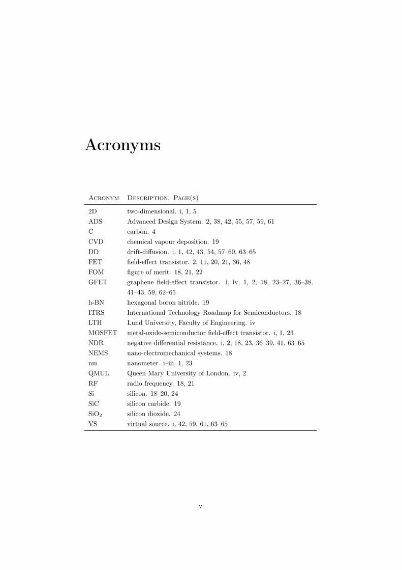
Acronyms
Acronym Description. Page(s)
2D two-dimensional. i, 1, 5ADS Advanced Design System. 2, 38, 42, 55, 57, 59, 61C carbon. 4CVD chemical vapour deposition. 19DD drift-diffusion. i, 1, 42, 43, 54, 57–60, 63–65FET field-effect transistor. 2, 11, 20, 21, 36, 48FOM figure of merit. 18, 21, 22GFET graphene field-effect transistor. i, iv, 1, 2, 18, 23–27, 36–38,
41–43, 59, 62–65h-BN hexagonal boron nitride. 19ITRS International Technology Roadmap for Semiconductors. 18LTH Lund University, Faculty of Engineering. ivMOSFET metal-oxide-semiconductor field-effect transistor. i, 1, 23NDR negative differential resistance. i, 2, 18, 23, 36–39, 41, 63–65NEMS nano-electromechanical systems. 18nm nanometer. i–iii, 1, 23QMUL Queen Mary University of London. iv, 2RF radio frequency. 18, 21Si silicon. 18–20, 24SiC silicon carbide. 19SiO2 silicon dioxide. 24VS virtual source. i, 42, 59, 61, 63–65
v

Notations
Notation Description. Page(s)
α Capacitance weighting factor. 27, 45, 46, 58, 59aC−C The carbon-carbon distance, approximately 1.42 Å [6]. 5–8, 16,
72, 74Av Intrinsic voltage gain. 18, 21, 23c Speed of light. 9, 13–15Cox−back Back-gate oxide capacitance. 27, 46, 48, 55–57Cox−top Top-gate oxide capacitance. 27, 46, 48, 55–57, 60Cq Quantum capacitance. 27, 45–47, 55, 56, 64∆ Spatial inhomogeneity of potential. 50, 56E Energy. 7–9, 13, 14, 16, 67–69, 73–76E Electric field. 44Ed Energy at Dirac point. 10, 11, 24–26, 28–31, 34, 35, 46, 48, 54Ef Fermi energy. 10, 11, 24–26, 28–31, 34, 35, 46, 48, 54εox−back Back-gate oxide permittivity. 27, 56εox−top Top-gate oxide permittivity. 27, 56fmax Maximum oscillation frequency. 18, 22fT Cut-off frequency. 18, 22, 23gm Transconductance. 21, 53H Hamiltonian operator. 67–69, 71–74, 76S Overlap integral. 68–71h Planck constant, 6.626 · 10−34 Js [7].h0 Hopping integral between nearest atom neighbours, see equa-
tion (A.26). 7, 73, 74h1 Hopping integral between next-nearest atom neighbours, see
equation (A.35). 7, 74~ Reduced Planck constant, h/(2π), see h. 8, 9, 11, 13, 14, 16,
26, 27, 46, 48, 50, 53, 56, 57, 75, 76
vi

Notation Description. Page(s)
Ids Current between drain and source. 21, 34, 37–39, 42, 44, 54–59,61, 65
k Boltzmann constant, 1.38 · 10−23 J/K, [7]. 11, 14, 26, 27, 45,46, 48, 54, 56, 57, 60
k Wave vector, (kx, ky). 7–9, 13, 14, 67, 70, 72–76kx Wave number in x-direction. 7, 72, 74–76ky Wave number in y-direction. 7, 16, 72, 74–76L Transistor channel length. 1, 44, 54–56, 58–60λ Mean free path. 1, 16, 43m Mass. 9, 13, 14n Electron density. 10, 11, 25, 26, 38, 48, 50, 52npud Charge density for electron-hole puddles.. 50, 52, 55, 57–59, 62,
63Ω The optical phonon energy. 53p Hole density. 10, 11, 25, 26, 38, 48, 50, 52Q Transport sheet charge density. 42, 44, 48, 54–56, 58, 60, 63q Elementary charge. 25–27, 45, 46, 48, 50, 53, 55–58, 60Qnet Net mobile sheet charge density. 48, 49, 53Qt Charge density relevant for transport. 48–50Qtot Total charge density relevant for transport.. 50T Temperature in Kelvin, T=300K in all calculations. 11, 26, 27,
45, 46, 48, 54, 56, 57, 60tox−back Back-gate oxide thickness. 27, 56tox−top Top-gate oxide thickness. 27, 56, 60, 63µ Mobility. 44, 48, 50–52, 54–56, 58–60V Channel-to-ground potential. 27, 29, 44, 55, 56, 64Vch Channel potential. 23, 25–31, 33–36, 38, 40, 44–48, 50, 52, 53,
55–59, 64Vdirac Gate voltage at Dirac point. 11, 24, 28, 29, 35Vdirac−0 Gate voltage at Dirac point when Vds = 0. 25, 29–31, 33–36Vdirac−0−back Back gate voltage at Dirac point when Vds = 0 and Vgs−top = 0.
26, 37–40, 56Vdirac−0−top Top gate voltage at Dirac point when Vds = 0 and Vgs−back = 0.
26, 37–40, 56, 60vdrift Drift velocity. 42, 44, 60, 61Vds Drain-to-source potential. 24–31, 33–41, 44, 54–61, 64, 65vF Fermi velocity for graphene approximately 106 m/s [8–10]. 8,
11, 15, 16, 26, 27, 46, 48, 50, 52–57, 59, 75, 76
vii

Notation Description. Page(s)
Vfb Flat-band voltage. 25Vgs Gate-to-source potential. 21, 24, 27–31, 33–40, 60Vgs−back Back-gate-to-source potential. 24, 26, 27, 37–40, 56Vgs−top Top-gate-to-source potential. 24, 26, 27, 38, 56Vin Input potential. 21Vout Output potential. 21vsat Velocity saturation. 44, 48, 52–54, 56, 58–60, 64φt The thermal voltage kT/q. 60W Transistor channel width. 42, 44, 54–56, 58, 61ψ The orbital wavefunction. 67–70, 72, 73, 75, 76
viii

Contents
Abstract i
Populärvetenskaplig sammanfattning ii
Preface iv
Acronyms v
Notations vi
1 Introduction 11.1 Background . . . . . . . . . . . . . . . . . . . . . . . . . . . . . . 11.2 Aim . . . . . . . . . . . . . . . . . . . . . . . . . . . . . . . . . . 21.3 Report Structure . . . . . . . . . . . . . . . . . . . . . . . . . . . 2
2 Graphene 42.1 Atomic Structure . . . . . . . . . . . . . . . . . . . . . . . . . . . 42.2 Band Structure . . . . . . . . . . . . . . . . . . . . . . . . . . . . 62.3 Anti-particles . . . . . . . . . . . . . . . . . . . . . . . . . . . . . 92.4 Local Equilibrium . . . . . . . . . . . . . . . . . . . . . . . . . . 102.5 Charge Density . . . . . . . . . . . . . . . . . . . . . . . . . . . . 102.6 Klein Tunnelling . . . . . . . . . . . . . . . . . . . . . . . . . . . 11
2.6.1 Single relativistic electron . . . . . . . . . . . . . . . . . . 132.6.2 Massless relativistic particle . . . . . . . . . . . . . . . . . 14
2.7 Physical Parameter Values . . . . . . . . . . . . . . . . . . . . . . 162.8 Applications . . . . . . . . . . . . . . . . . . . . . . . . . . . . . . 18
3 Field-Effect Transistor 203.1 Analogue Amplifier . . . . . . . . . . . . . . . . . . . . . . . . . . 21
ix

4 Graphene Field-Effect Transistor 234.1 Basic Principles . . . . . . . . . . . . . . . . . . . . . . . . . . . . 244.2 Carrier Density Inside the Channel . . . . . . . . . . . . . . . . . 25
4.2.1 Channel Potential . . . . . . . . . . . . . . . . . . . . . . 254.2.2 Biasing Configurations . . . . . . . . . . . . . . . . . . . . 27
4.3 Negative Differential Resistance . . . . . . . . . . . . . . . . . . . 364.3.1 Theoretical Explanation . . . . . . . . . . . . . . . . . . . 37
5 Modelling Graphene Field-Effect Transistor 425.1 Ballistic Transport . . . . . . . . . . . . . . . . . . . . . . . . . . 43
5.1.1 Quasi-Ballistic Transport . . . . . . . . . . . . . . . . . . 435.2 Drift-Diffusion Model . . . . . . . . . . . . . . . . . . . . . . . . 43
5.2.1 Drift Velocity and New Current Expression . . . . . . . . 445.2.2 Capacitance Weighting Factor . . . . . . . . . . . . . . . . 455.2.3 Quantum Capacitance . . . . . . . . . . . . . . . . . . . . 465.2.4 dV/dVch . . . . . . . . . . . . . . . . . . . . . . . . . . . 465.2.5 Carrier Density . . . . . . . . . . . . . . . . . . . . . . . . 485.2.6 Mobility . . . . . . . . . . . . . . . . . . . . . . . . . . . . 505.2.7 Velocity Saturation . . . . . . . . . . . . . . . . . . . . . . 525.2.8 Simulation Model 1 . . . . . . . . . . . . . . . . . . . . . 545.2.9 Simulation Model 2 . . . . . . . . . . . . . . . . . . . . . 565.2.10 Simulation Model 3 . . . . . . . . . . . . . . . . . . . . . 57
5.3 Virtual Source Model . . . . . . . . . . . . . . . . . . . . . . . . . 595.3.1 Simulation Model 4 . . . . . . . . . . . . . . . . . . . . . 61
6 Discussion of Result 626.1 Further Work . . . . . . . . . . . . . . . . . . . . . . . . . . . . . 65
Appendices 66
A Graphene energy dispersion using tight-binding approximation 67
B Weyl Hamiltonian for graphene 75
x
Chapter 1
Introduction
1.1 Background
In 1965, Gordon E. Moore published the paper Cramming more componentsonto integrated circuits [11]. In the paper, Moore projected that the numberof transistors per integrated circuit would have an annual doubling. Mooreupdated his prediction in 1975, to a doubling every second year. Today, theprediction is commonly known as “Moore’s law” and even though over half acentury has passed, the prediction is still true [12]. Transistors with 20 nanome-ter (nm) channel length are in mass production and many researchers believethat we are reaching a limit with downsizing conventionally used silicon metal-oxide-semiconductor field-effect transistors (MOSFETs) [1]. To keep up withthe trend of making the transistor smaller, new channel materials are studiedand graphene has come into the spotlight. Graphene became a serious contendermostly due to its high mobility, but other properties such as high velocity sat-uration and the two-dimensional (2D) nature of the material have gained moreattention in recent years [2–4].
The first graphene MOSFET was reported in 2007 [13] and since then, a num-ber of graphene field-effect transistors (GFETs) have been fabricated [3]. Eventhough plenty of working transistors have been created, modeling GFETs re-mains complicated and complex. Several GFET models using the drift-diffusion(DD) model have been presented in the past [14–16]. These models are onlyvalid when the channel length L is longer than the mean free path λ, otherwiseshort channel effects have to be taken into consideration. As the down-scalingof transistors and GFETs continues, it remains important to create accuratemodels that do not ignore the effects that occur in short channel devices.
1

1.2 Aim
As far as developing simulation models is concerned, one of the greatest chal-lenges lies in combining high accuracy with simple mathematics, the latter toallow implementation and model understanding. To create accurate models,it is important to have good fundamental knowledge. I have experienced thatthere are many articles with advanced GFETs simulation models, but few thatexplain the particular behaviours that we see in GFETs.
Therefore, the main goal of the Master’s thesis is to describe, explain, show-case along with mathematically prove the different behaviours in GFETs. Iwant to showcase equations as well as visual images to simplify the understand-ing of the complicated behaviours of GFETs. I hope to create a good basis, forsomeone to read who is interested in modelling GFETs.
This thesis work will then use the theory when comparing some differentsimulation models. I will look into how they are built and how this ties inwith the theory. I aim to get an understanding of why different models giveaccurate and inaccurate results, as well as which approximations work and why.I will only look at models that can or have been implemented in the hardwaredescription language Verilog-A. These models can be run with the simulationprogram Advanced Design System (ADS) [17]. I will use MATLAB [18] toanalyse, compare and verify equations at earlier stages.
During my studies, I have always been encouraged to do background researchand understand the usefulness of my work result, which is why a part of mythesis report will focus on the state of art, prospects and obstacles of grapheneas well as GFETs.
My thesis work will take place at Queen Mary University of London (QMUL),in the Electronics department. At the department, a group of people are focus-ing on negative differential resistance (NDR) in GFETs. Therefore I will favourmodels that manage to showcase that particular phenomena. I will also focuson understanding the different explanations for the phenomena.
1.3 Report Structure
This report focuses greatly on the theory behind GFET. Chapter 2 Grapheneexplores graphene from the atomic to the practical scale. It is followed byChapter 3 Field-Effect Transistor, that gives a general introduction to field-effecttransistors (FETs). Chapter 4 Graphene Field-Effect Transistor and Chapter 5Modelling Graphene Field-Effect Transistor both focus on GFETs, the first onthe theory and visual representation to understand the transport behaviours,while the latter presents different simulation models. Finally, concluding with
2

Chapter 6 Discussion of Result that discusses the different models together withan idea of what I think can be done in future work. A list of acronyms as wellas notations are shown in the pre-matter, please refer back to these lists if anabbreviation is unclear.
3
Chapter 2
Graphene
Graphene is a fascinating material that not only conducts heat and electricitybetter than any other metal, but is also transparent and flexible. The ma-terial can withstand mechanical deformation and be folded without breaking.Graphene has high impermeability for gases and is chemically inert and stable.What makes graphene unique and so intriguing is that all these sought-afterproperties are combined into one single material [3].
In this chapter, graphene is described in depth. The chapter starts of onthe atomic scale and continues to up-scale to the band structure, charge densityand concludes with graphene applications.
2.1 Atomic Structure
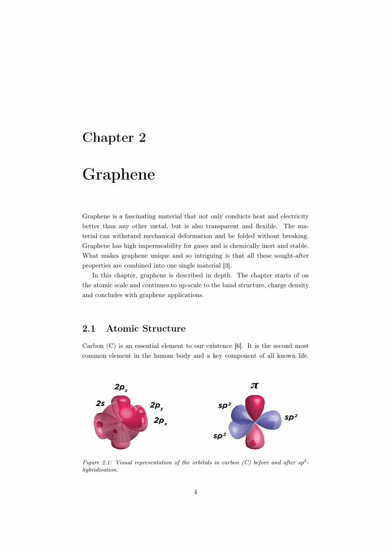
Carbon (C) is an essential element to our existence [6]. It is the second mostcommon element in the human body and a key component of all known life.
2s
2px
2pz
π
sp2
sp2
sp22py
Figure 2.1: Visual representation of the orbitals in carbon (C) before and after sp2-hybridisation.
4
Still, it was very recently discovered that carbon in its two-dimensional (2D)form, can be stable under ambient conditions [10].
Carbon has got four valence electrons in the 2s, 2px, 2py and 2pz or-bitals. Through sp2-hybridisation, three sp2 orbitals are created, connectingeach orbital to the adjacent carbon neighbour with a strong covalent in-planeσ-bond [6, 19]. The connected carbon atoms create a single-layered honeycombstructure material known as graphene [3, 6, 20]. The last valence electron, fromthe 2pz orbital, creates the π-orbital perpendicular to the other orbitals. Theπ-orbitals define the thickness and enable high conductivity in graphene [19],which is why graphene under many circumstances can be treated as a materialwith just one conduction electron per atom [21].
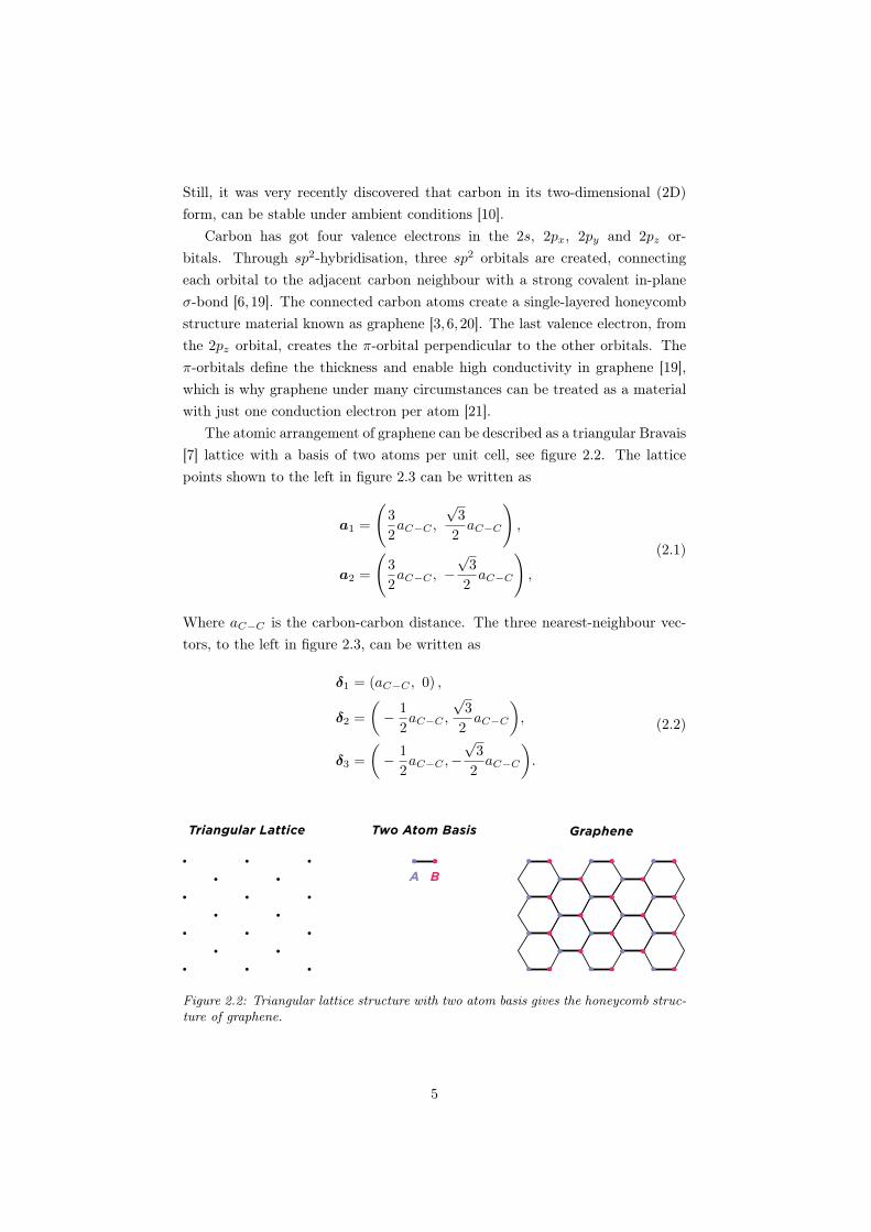
The atomic arrangement of graphene can be described as a triangular Bravais[7] lattice with a basis of two atoms per unit cell, see figure 2.2. The latticepoints shown to the left in figure 2.3 can be written as
a1 =
(3
2aC−C ,
√3
2aC−C
),
a2 =
(3
2aC−C , −
√3
2aC−C
),
(2.1)
Where aC−C is the carbon-carbon distance. The three nearest-neighbour vec-tors, to the left in figure 2.3, can be written as
δ1 = (aC−C , 0) ,
δ2 =
(− 1
2aC−C ,
√3
2aC−C
),
δ3 =
(− 1
2aC−C ,−
√3
2aC−C
).
(2.2)
GrapheneTwo Atom Basis
A B
Triangular Lattice
Figure 2.2: Triangular lattice structure with two atom basis gives the honeycomb struc-ture of graphene.
5

b1
b2
a1
∂1
∂2
∂3
a2
Reciprocal SpaceReal Space
Figure 2.3: Lattice structure for graphene, in real (left) and reciprocal space (K-space)(right).
The Wigner-Seitz cell definition is typically used to describe the primitivecell in a crystal. The area of the Wigner-Seitz cell is defined as containingexactly one Bravais lattice point (in this case the basis of two atoms) as well asthe area constructed by separating the bisectors in between each lattice pointwith perpendicular lines. The hexagonal Wigner–Seitz cell for graphene, in realspace, is shown in figure 2.3 to the left.
Real space gives a good understanding of the atomic arrangement, but someaspects are difficult to showcase, therefore reciprocal space (also known as mo-mentum space or K-space) can be used. For example, reciprocal space showswave interactions more clearly, which is useful when working with electronicmaterials on a low scale [22]. After conversion, the reciprocal lattice vectors, a1
and a2 in figure 2.3, can be written as
b1 =
(2π
3aC−C,
2π√3aC−C
),
b2 =
(2π
3aC−C, − 2π√
3aC−C
).
(2.3)
The Wigner-Seitz cell in reciprocal space, commonly known as the the firstBrillouin zone [6, 23], is marked to the right in figure 2.3.
2.2 Band Structure
Graphene can, as was mentioned earlier, be treated as a material containing onlyone conduction electron per atom [21]. Therefore, to get a better understandingof graphene, it is wise to look at the energy dispersion (band structure) of the
6
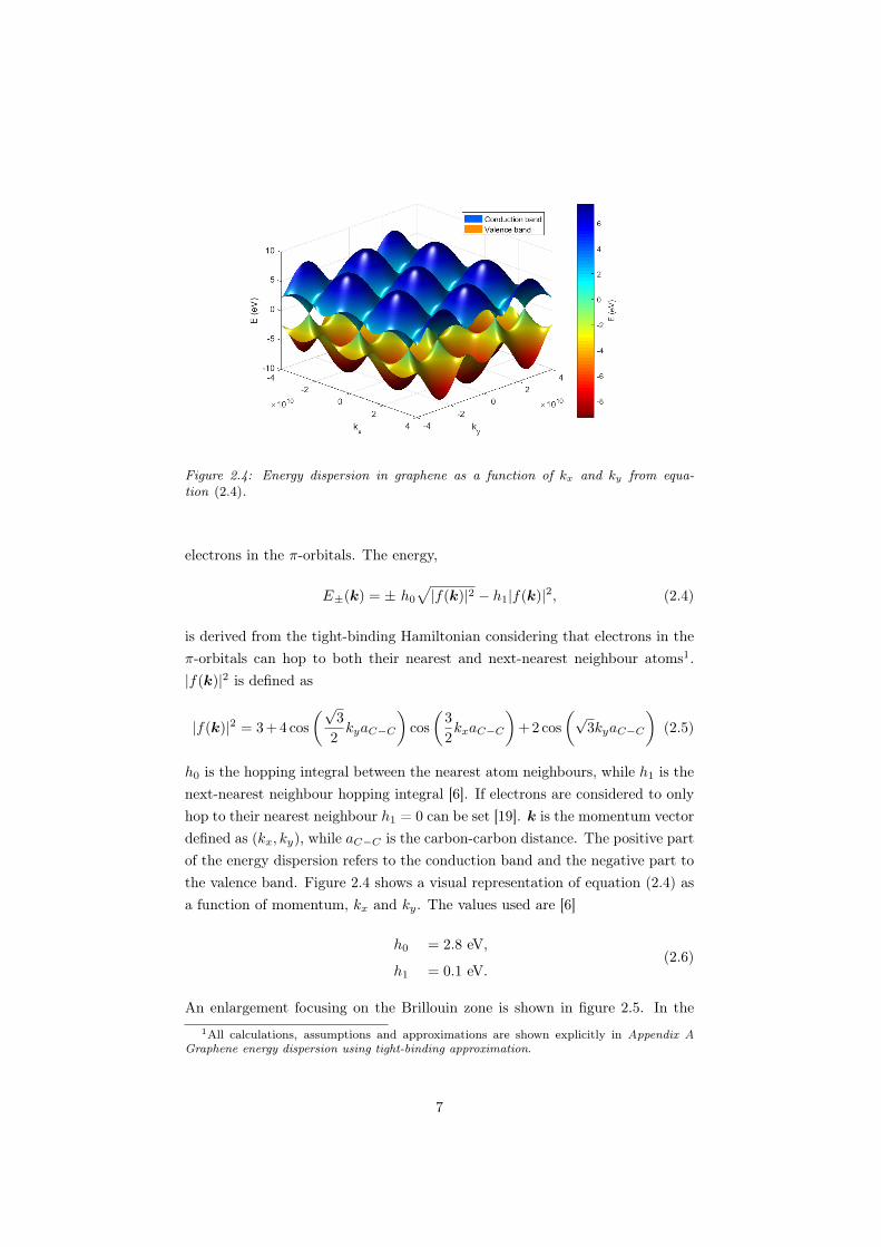
Figure 2.4: Energy dispersion in graphene as a function of kx and ky from equa-tion (2.4).
electrons in the π-orbitals. The energy,
E±(k) = ± h0
√|f(k)|2 − h1|f(k)|2, (2.4)
is derived from the tight-binding Hamiltonian considering that electrons in theπ-orbitals can hop to both their nearest and next-nearest neighbour atoms1.|f(k)|2 is defined as
|f(k)|2 = 3 + 4 cos
(√3
2kyaC−C
)cos
(3
2kxaC−C
)+ 2 cos
(√3kyaC−C
)(2.5)
h0 is the hopping integral between the nearest atom neighbours, while h1 is thenext-nearest neighbour hopping integral [6]. If electrons are considered to onlyhop to their nearest neighbour h1 = 0 can be set [19]. k is the momentum vectordefined as (kx, ky), while aC−C is the carbon-carbon distance. The positive partof the energy dispersion refers to the conduction band and the negative part tothe valence band. Figure 2.4 shows a visual representation of equation (2.4) asa function of momentum, kx and ky. The values used are [6]
h0 = 2.8 eV,
h1 = 0.1 eV.(2.6)
An enlargement focusing on the Brillouin zone is shown in figure 2.5. In the1All calculations, assumptions and approximations are shown explicitly in Appendix A
Graphene energy dispersion using tight-binding approximation.
7
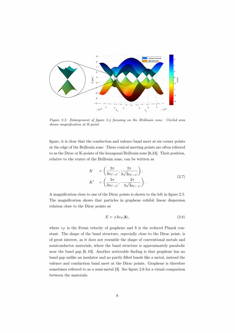
Figure 2.5: Enlargement of figure 2.4 focusing on the Brillouin zone. Circled areashows magnification at K-point.
figure, it is clear that the conduction and valence band meet at six corner pointsat the edge of the Brillouin zone. These conical meeting points are often referredto as the Dirac or K-points of the hexagonal Brillouin zone [6,24]. Their position,relative to the centre of the Brillouin zone, can be written as
K =
(2π
3aC−C,
2π
3√
3aC−C
),
K ′ =
(2π
3aC−C,− 2π
3√
3aC−C
).
(2.7)
A magnification close to one of the Dirac points is shown to the left in figure 2.5.The magnification shows that particles in graphene exhibit linear dispersionrelation close to the Dirac points as
E = ±~vF |k|, (2.8)
where vF is the Fermi velocity of graphene and ~ is the reduced Planck con-stant. The shape of the band structure, especially close to the Dirac point, isof great interest, as it does not resemble the shape of conventional metals andsemiconductor materials, where the band structure is approximately parabolicnear the band gap [6, 10]. Another noticeable finding is that graphene has noband gap unlike an insulator and no partly filled bands like a metal, instead thevalence and conduction band meet at the Dirac points. Graphene is thereforesometimes referred to as a semi-metal [3]. See figure 2.6 for a visual comparisonbetween the materials.
8

k
E
METAL
k
E
GRAPHENEINSULATOR
k
E
Figure 2.6: Energy dispersion for an insulator, a metal and graphene.
2.3 Anti-particles
The linear energy dispersion of graphene closely resembles the Dirac spectrumof massless Dirac particles [6]. An essential feature of the Dirac spectrum isthe existence of anti-particles: electrons and positrons (fermions). For Diracparticles with massm, there is an energy band gap between the minimal electronenergy, E0 = mc2, and the maximal positron energy, −E0. This means that thesize of the energy band gap depends on the mass of the fermions, decreasing forparticles with less mass. Far away from the band gap, the energy of the Diracfermion depends linearly on the wave vector as
E = ±~c|k|, (2.9)
where c is the speed of light. For Dirac particles without mass the band gap iszero and the linear relation, in equation (2.9), holds at any energy [10]. Thislinear energy dispersion in massless Dirac fermions, is very similar to thatof graphene, which is why graphene is often compared with massless Diracfermions. It is an interesting similarity since it explains a lot of the specificcharacteristics in graphene, that are normally seen for Dirac particles. Morespecifically for graphene, this means that for any electron state with a positiveenergy E, a corresponding conjugated hole state with energy -E must exist.This property is often referred to as the charge-conjugation symmetry [9,10,24].Electrons and holes in graphene are interconnected, which is rare in other com-monly used materials where electrons and holes are described by separate (non-connected) Schrödinger equations [6, 8].
9

-0.2 -0.15 -0.1 -0.05 0 0.05 0.1 0.15 0.2
Ef - E
d [eV]
0
0.5
1
1.5
2
2.5
3
3.5
Carr
ier
density [cm
-2]
×1012
n
p
n+p
Figure 2.7: Carrier densities for electrons n and holes p, versus the difference betweenthe Fermi level and the Dirac point Ef − Ed.
2.4 Local Equilibrium
Before merging further into the traits of graphene it is important to clarifysome expressions. A system that does not exchange matter or heat with thesurroundings, where the variables of the system are independent of time but varywith position, is said to be in non-uniform equilibrium. For a system to be innon-uniform equilibrium the electrochemical potential, also known as the Fermilevel, has to be constant. If a voltage is applied over a graphene sheet the Fermilevel cannot be constant and non-uniform equilibrium cannot be established.But, if in some small neighbourhood of a point one can assume that the potentialis close to constant the system is said to be in local (non-uniform) equilibrium.For these local points quasi-Fermi levels can be established [25]. In this reportthe expression Fermi level, with the notation Ef , will be used for both Fermilevels and quasi-Fermi levels . Now that the notation of Ef has been clarifiedlet us move on to the charge density.
2.5 Charge Density
At absolute zero temperature, in neutral and discrepancy free graphene, thevalence band is completely filled and the conduction band is empty, meaningthat the Fermi level Ef goes straight through the Dirac point Ed [21]. Howeverif a potential is applied, creating an electric field, the Fermi level moves whichtherefore change the charge density. For electrons and holes, the charge densities
10

can be expressed as
n =2(kT )2
π(~vF )2F1
(Ef − EdkT
), (2.10)
p =2(kT )2
π(~vF )2F1
(−Ef − Ed
kT
). (2.11)
F1(·) is the first-order Fermi-Dirac integral, k is Boltzmann constant and Ef−Edis the distance between the Fermi level and the Dirac point. As |Ef − Ed|gets larger, the total charge density n + p, will increase, thereby increasingthe conductivity and thus making graphene more metallic [7]. This effect isknown as the electric field effect, and was shown experimentally in one of thefirst publications about graphene. The effect is a fundamental trait used inelectronic devices, for example in field-effect transistors (FETs) [26].
Unfortunately, graphene is normally not as simple as described above. Itis common that, even in unloaded graphene, due to discrepancies and imper-fections as well as materials in conjunction interacting with graphene, thatEf 6= Ed [6]. This means that the conductivity minimum might might oc-cur when no potential is applied, but rather when a specific potential is appliedmoving the levels so that Ef = Ed. The potential needed is referred to as theDirac voltage Vdirac [20].
2.6 Klein Tunnelling
In conventional mechanics, where particles is described as point masses, par-ticles cannot propagate through a region where the potential energy is higherthan the total energy of the particle. However, in (non-relativistic) quantummechanics, particles are described by a probability wave from the Schrödingerequation. When a probability wave hits a potential barrier, it will go inside thebarrier, contrary to conventional mechanics. The wave will decay exponentiallyinside the barrier, with greater damping for higher barriers. For thick and highbarriers, the wave will be very dampened for a long period, so that only a tinypart or no part at all comes out on the other side of the barrier. Hence, theprobability of tunnelling and the transmission coefficient will be small. How-ever, for a thinner and lower barriers a greater part of the probability wave canpenetrate, which increases the probability of tunnelling and gives a higher trans-mission coefficient. This phenomena, when the total energy of the particle doesnot exceed that of the potential barrier, but it still goes through the barrier, isknown as quantum tunnelling [27].
Then again, as we have discovered electrons and holes in graphene are notdescribed by the Schrödinger equation. So, it is intriguing to see what happens
11
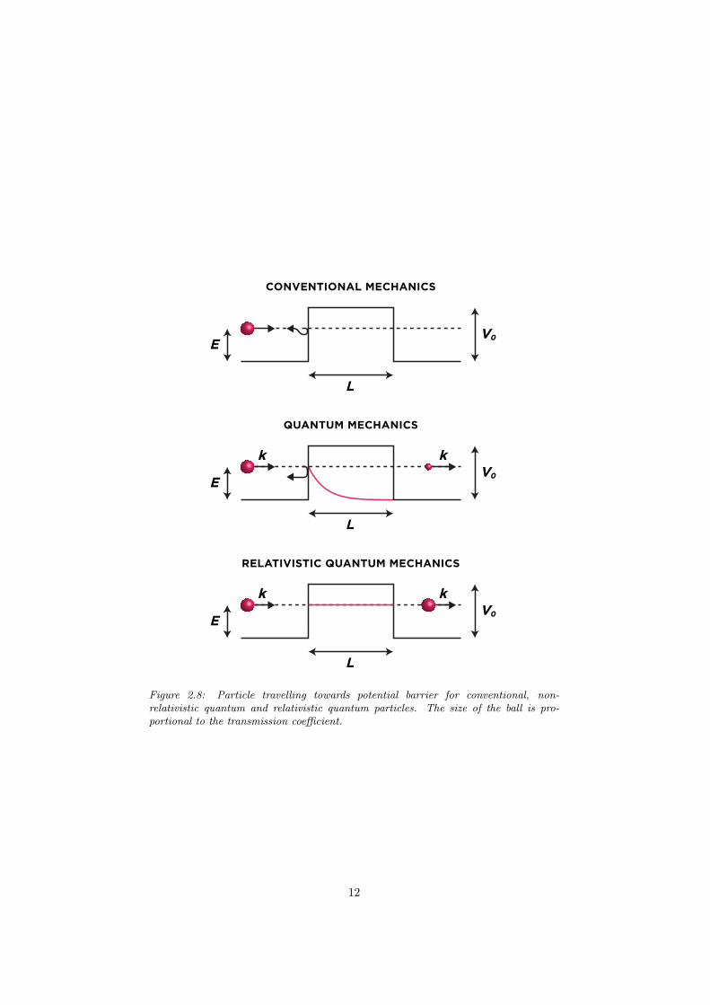
CONVENTIONAL MECHANICS
V0E
L
L
V0E
k k
QUANTUM MECHANICS
L
V0E
k k
RELATIVISTIC QUANTUM MECHANICS
Figure 2.8: Particle travelling towards potential barrier for conventional, non-relativistic quantum and relativistic quantum particles. The size of the ball is pro-portional to the transmission coefficient.
12

-0.8 -0.6 -0.4 -0.2 0.2 0.4 0.6 0.8
×1012
-1
-0.5
0.5
1
×106
k
E (eV)
E+
E-
L
R
Figure 2.9: Energy dispersion for relativistic electrons from equation (2.12). L and Rrepresents asymptotes and when the mass m goes to zero.
the Dirac equation is applied to the barrier problem. To get a better under-standing of the problem, let us start by looking at what happens with a singlerelativistic electron.
2.6.1 Single relativistic electron
The energy eigenvalues of the Dirac equation for a single relativistic electron,with mass m, can be written as
E = ±√
(~ck)2 + (mc2)2, (2.12)
and is shown visually in figure 2.9. The upper branch E+ represents the positivepart of the equation and the lower branch E− represent the negative part of theequation. From the figure it can be seen that, for real values of k we must haveE > mc2 or E < −mc2. Let us imagine that an electron is in a positive energystate E+ and that it is travelling in the positive x-direction as seen in figure 2.9.At some point the electron encounters a potential barrier V0. If E − V0 > mc2
the electron will continue travelling in the positive x-direction, but with a wavenumber that now has to satisfy
E − V0 =√
(~ck)2 + (mc2)2. (2.13)
13
Equation (2.13) can only be satisfied if k2 > 0, which means that k cannot beimaginary. For positive group velocity, k also has to be positive. On the otherhand, if the potential very high so that E−V0 < −mc2, the wave number mustsatisfy
E − V0 = −√
(~ck)2 + (mc2)2. (2.14)
For equation (2.14) to be satisfied k cannot be imaginary. The electron will bein the E− branch, but for it to have a positive group velocity, k also have to benegative. This means that the particle continues to propagate in the positivex-direction with a negative k-value. This is what Klein noted in his famouspublication Die Reflexion von Elektronen an einem Potentialsprung nach derrelativistischen Dynamik von Dirac from 1929 [28].
If the value of V0 is something in between our two examples, −mc2 <
E − V0 < mc2, then the dispersion relationship in equation (2.12) can onlybe satisfied if k2 < 0. That means that k has to be imaginary. An imaginarywave number gives a exponential decay, just like in quantum mechanics, there-fore if this condition is fulfilled, the wave will be completely or partly reflected.
Perfect transmission is accomplish if the value of V0 goes to infinity, thisis the phenomena known as Klein paradox [29]. The essence of the paradoxlies in the prediction that when a relativistic quantum particle, described bythe Dirac equation, travels towards a barrier, such as in figure 2.8, the barrierbecomes more transparent with increased potential V0, in contrast to a conven-tional non-relativistic particle, described by the Schrödinger equation, where theprobability of tunnelling decreases with increased potential [8]. Even though theparadox is well accepted there are still different theoretical explanations [30].One common and intuitive explanation is that, a strong potential is repulsivefor electrons but attractive for holes, which results in holes being carriers [31].
2.6.2 Massless relativistic particle
When the massm, in equation (2.12) and figure 2.9, goes towards zero the energydispersion E will coincide with the two lines L and R. Particles belonging toline L have a negative group velocity, therefore travelling in the left direction,while particles on line R have a positive group velocity and will travel in theright direction. This means that there is no gap between the lowest energy ofE+ and the highest energy of E−, hence there is no imaginary k-phase wherethe wave can be reflected. The expression,
E = ±~c|k|. (2.15)
always holds for the massless case [29]. Once again it is noticable that equa-
14

L
V0E
Figure 2.10: Klein tunnelling in graphene.
tion (2.15) is very similar to equation (2.8), except that the speed of light c, isused instead of the Fermi velocity vF ≈ c/300 [8].
The transmission probability for particles in graphene is derived to furtheremphasise the theory of Klein tunnelling. For simplicity, a perfectly rectangularpotential barrier such as
V (x) =
V0, if 0 < x < L
0, otherwise,(2.16)
is used, see figure 2.10. The Dirac-like Hamiltonian for graphene, sometimesreferred to as the Weyl Hamiltonian2, in equation (B.10), is used together witha factor for the potential barrier V0. The incoming graphene particle is assumedto propagate with an angle γ1 in respect to the x-axis. The expression for thetransmission probability can be written as [8]
T = 1− |r|2
= 1−
∣∣∣∣∣∣∣∣2ieiγ1 sin(c1L)
sin(γ1)− c2 sin(γ2)
c2
(e−ic1L cos(γ1 + γ2) + eic1L cos(γ1 − γ2)
)− 2i sin(c1L)
∣∣∣∣∣∣∣∣2
(2.17)2The Weyl Hamiltonian is described further in Appendix B Weyl Hamiltonian for graphene
15

where the variables are defined as
c1 =
√(E − V0)2
~2vF 2− ky2, (2.18)
c2 = sgn(E) sgn(E − V0), (2.19)
γ2 = arctan
(kyc1
). (2.20)
Equation (2.17) can be simplified for when |V0| |E| as
T =cos2(γ1)
1− cos2(c1L) sin2(γ1). (2.21)
The result in equation (2.21) show that perfect transmission always occurs whenparticles travel parallel to the x-axis, in other words when γ1 = 0. The same ap-plies for all values that satisfy c1L = πn, n ∈ Z [8]. In summary, for high enoughbarriers particles, who travel parallel to the x-axis, tunnel through unimpeded.
Throughout this section we have seen why Klein tunnelling is such an impor-tant trait to consider for graphene. The key fact to remember for graphene, isthat both electrons and holes can be charge carriers in the channel at the sametime. In regions where the particle energy is higher than the barrier energy,charge transport is assured by electrons, whereas when the particle energy islower than the barrier energy, holes assure the charge transport role. Thereforein graphene devices, when one uses the term barrier, it does not indicate a re-gion with total reflection or exponential dampening, but rather a region wherecharge transport is undertaken by holes instead of electrons [9].
2.7 Physical Parameter Values
When using graphene in electronic application it is important to know its exactphysical parameter values. Table 2.1 contains a summary of important param-eters for graphene. These values are used in this work, unless otherwise stated.
Parameter Value Unit Reference
Carbon-carbon distance, aC−C 1.42 Å [6]Mean free path, λ 0.3 µm [20,32]Fermi velocity, vF 106 m/s [8–10]Maximum current density 108 A/cm2 [3, 20,33]Strength per density 48 000 kNm/kg [3]
Table 2.1: Physical properties of graphene
16

Figure 2.11: Visual representation of the strength of graphene [35].
The extreme strength shown in graphene is because of the strong σ-bondbetween the carbon atoms. Professor James Hone of Columbia University ex-pressed the strength of graphene in a very eloquent way [34]
Our research establishes graphene as the strongest material evermeasured, some 200 times stronger than structural steel. It wouldtake an elephant, balanced on a pencil, to break through a sheet ofgraphene the thickness of Saran Wrap.
A visual representation of the expression is shown in figure 2.11.Another well known and important trait for graphene is its mobility. The
high mobility has often been seen as the main reason why researchers have hadso high beliefs for material [3]. It has been shown that free standing graphenehas the highest carrier mobility of all semiconductors [36, 37]. The carrier mo-bility, for free standing graphene, is limited almost only by the acoustic phononscattering.
Yet, no parameter value for the mobility is shown in table 2.1. Grapheneis usually placed on or between materials, which due to Coulomb scatteringand optical surface phonons, decreases the mobility. Other factors such as thequality of graphene, temperature as well as applied electric field also effectsthe mobility in graphene [38]. To accurately calculate the carrier mobility, ina electronic device with graphene, these different effects have to be taken intoconsideration, hence why no static value can be added to table 2.1. The mobilityis discussed further in Section 5.2.6 Mobility.
17

2.8 Applications
The chapter is concluded with this final section on the prospects and obstaclesfor electronic graphene applications.
There are many different areas where graphene is a prosperous materialcandidate for electronic applications. Experts talk about graphene having a bigimpact in technological fields such as wearable and flexible devices, photonicdevices, nano-electromechanical systems (NEMS), solar cells, batteries, superdense data storages, bioelectronics as well as high-frequency devices. A closerlook into patent applications shows that the dominant fields are synthesis andelectronics which suggest that graphene is still at an early stage of development[3].
Graphene is process compatible with conventional processing of semicon-ductors, which puts the material in a favourable position [20]. Thanks to theprocess compatibility, it is possible to integrate graphene components in to sili-con (Si)-based electronics with the possibility of gradually replacing Si [3]. TheInternational Technology Roadmap for Semiconductors (ITRS) have stated thatthey consider graphene to be a possible candidate for post-Si electronics [39].
The first graphene integrated circuit, in which all components, includinginductors and graphene field-effect transistors (GFETs), integrated on a wafer,was created in 2011 [1]. Positive results from the circuit showed that graphenedevices with useful functionality and performance can be accomplished [3].
Using graphene as a channel material in transistors is an exciting idea be-cause of the high mobility, current density and because particles in grapheneshow relativistic behaviour [3]. However, graphene gives a poor on-off currentratio due to its lack of energy band, which is why it is not suitable for logic cir-cuits [16]. The missing band gap is often discussed as a big obstacle for graphenein electronic applications. A band gap can be opened, but it comes with thecost of decreased mobility. It has therefore been expressed that it would bebetter to use graphene in new applications rather than as a material to replaceSi [1]. One example is negative differential resistance (NDR), a phenomena thatis normally only seen in two-terminal devices [9].
In analogue and radio frequency (RF) circuits, a band gap is not as im-portant. Instead, other figure of merit (FOM) such as the intrinsic gain Av,maximum oscillation frequency fmax and cut-off frequency fT play larger role,all of which are possible to achieve without a band gap [16]. The theory ofintrinsic gain, maximum and cut-off frequency are described further in chapterChapter 3 Field-Effect Transistor.
For possible applications, the problems with manufacturing has to be over-come. The cost of manufacturing good quality graphene is today too high for
18

commercial use. Different techniques are developed and used to create graphene;micro-mechanical cleavage, chemical vapour deposition (CVD), growth on alter-native substrates as silicon carbide (SiC) and hexagonal boron nitride (h-BN)are among some of the most common techniques [3]. Micro-mechanical cleavagewas the technique originally used by Andre Geim and Konstantin Novoselov [40].The technique was for a long time the best to get large single crystalline struc-tures. It is still often used in fundamental research because of its low costand simplicity. In essence, the only tools needed are a pencil and some tape.CVD is a useful processing technique since it is used commercially for manyother materials, however the method still has to improve to consistently createlarge single crystalline graphene sheets. Growth on alternative substrates haveseveral benefits such as speed, better lattice match and higher control over thethickness to ensure that only one monolayer is deposited. But even though bothSiC and h-BN give better results quicker, the cost is still too high compared toconventionally used Si substrates. In 2011, the cost of SiC was about 25-30times more expensive than Si [3].
19

Chapter 3
Field-Effect Transistor
A field-effect transistor (FET) is an electronic device with at least three ter-minals: source, drain and gate. A channel, where the current can flow, is inbetween the source and drain. An insulator is placed in between the channeland the gate terminal. Figure 3.1 shows this conventional layout. In mostconventional FETs silicon (Si) is used as a channel material [3].
As its name suggests, FETs relies on an electric field. When a potentialis applied to the gate, an electric field is created. The electric field repelsor attracts electrons in the channel thereby altering the number of free chargecarriers (electrons or holes) available for conduction, hence changing the channelconductivity [41]. The transistor is in its on-state when the free carrier densityin the channel is high, on the contrary when the free carrier density is lowthe transistor is said to be in its off-state. Conventional FETs are unipolartransistors meaning that the majority charge carriers in the channel are electronsor holes [20].
Source
Top-gate
Insulator
ChannelSubstrate
Drain
Figure 3.1: Layout of typical FET.
20

3.1 Analogue Amplifier
FETs can be used in logic or analogue and radio frequency (RF) applications. Inthe latter case, the FETs are commonly used as analogue amplifiers. A typicalset-up is shown in figure 3.2. A potential Vgs applied between gate and source,controls the current Ids flowing between drain and source. The current Idsflows through the resistor RL, causing a voltage drop and therefore the outputpotential Vout is altered. The difference between the output Vout and inputvoltage Vin = Vgs gives the important figure of merit (FOM) called intrinsicvoltage gain,
Av =VoutVin
=VoutVgs
. (3.1)
From the definition, it can be seen that the intrinsic voltage gain depends onboth the transconductance,
gm =dIdsdVgs
, (3.2)
and the load resistance, RL. To improve the value of Av, large currents mustbe achieved. This can be done by enhancing the carrier concentration andvelocity. There are different methods that can be used for enhancement, somecommon methods include channel doping, channel material choice as well as sizereduction of channel and gate insulator [20].
Vgs
=
Vin
Vout
RL
GD
S
Figure 3.2: Schematic of an analogue amplifier using FET.
Voltage gain Av > 1 is required in general-purpose electronic circuits, suchas analogue voltage amplifiers and digital logic gates. [3]
21
Two other important FOM is the cut-off frequency fT and the maximumoscillation frequency fmax. The cut-off frequency is defined as the frequencyat which the energy flowing through the system is no longer attenuated. Thisoccurs when intrinsic current gain decreases to unity, so that the current gainis 0 dB . The maximum oscillation frequency on the other hand, is defined asthe frequency at which the power gain is 0 dB [7].
22
Chapter 4
Graphene Field-EffectTransistor
In graphene field-effect transistors (GFETs), the channel material is graphene.The first GFET was reported in 2004, this was a back-gated device that showedthat it was possible to use graphene as a channel material. However, the tran-sistor had intrinsic voltage smaller than unity Av < 1, and it suffered fromlarge parasitic capacitances and therefore could not be integrated with othercomponents [3]. The first graphene metal-oxide-semiconductor field-effect tran-sistor (MOSFET) was reported in 2007. The results showed that the currentcould be controlled with the applied gate voltage and the envisaged capabil-ity of GFETs was confirmed [13]. After that a number of transistors, that usegraphene as a channel material, have been successfully fabricated [3]. In 2010, areport showed a successful fabrication of a GFET with Av > 1 [42]. Year 2012,a group of researchers fabricated a GFET with 67 nanometer (nm) gate lengthand the impressive cut-off frequency fT = 427 GHz [43]. The fast developmentof GFETs is a good indicator for the potential of the device.
In this chapter we will discuss the theory behind GFETs. The chapter beginswith Section 4.1 Basic Principles where the basic principles are explained alongwith some notations. Section 4.2 Carrier Density Inside the Channel furtherexplores the carrier density as well as the channel potential Vch, for differentbiasing conditions. The chapter is concluded with Section 4.3 Negative Differ-ential Resistance, where the theoretical explanation as well as needed biasingconditions for negative differential resistance (NDR) are discussed.
23

4.1 Basic Principles
A very basic GFET-layout is used in this work. Starting with a wafer, an oxidelayer is deposited. The oxide both acts as a back-gate oxide as well as a materialonto which graphene can be grown more easily. The combination of silicon (Si)wafer and silicon dioxide (SiO2) is commonly mentioned in literature [3,44,45].On the oxide the graphene layer is grown, and subsequently the source and drainterminals as well as the gate-oxide and the gate terminal. The back terminal isplaced at the bottom of the sample. See figure 4.1 for a visual representation. Itis conventional to ground the source and consider it the reference potential in thedevice [16]. For simplicity, only the part under the gate terminal is consideredin GFET simulations, this region is called the intrinsic device [14].
SourceTop-gate
Top-oxide
Graphene
Drain
Back-gate
Back-oxide
Substrate
Figure 4.1: Layout of typical GFET.
The carrier concentration in the channel is modulated by the applied gate-to-source voltage Vgs. In figure 4.1, as in many GFETs, two gates are usedto modulate the potential: top-gate Vgs−top and back-gate Vgs−back [16]. Theapplied voltages creates a field-effect in the channel which repels or attractselectrons or holes. To achieve a high effect for the applied potentials Vgs−topand Vgs−back, it is important to use thin and high-K (dielectric constant) oxidesbetween the gates and the channel [3].
The Dirac voltage Vdirac, is a parameter commonly used in analysis, mod-elling and discussions of GFETs. We have earlier in this report defined it as thegate potential when the Fermi-level Ef , passes through the Dirac point Ed, seeSection 2.5 Charge Density. This still holds true for GFETs, if there is no chargedifference between source and drain Vds = 0. For that particular case one couldthink of Vdirac as the gate potential where the majority charge concentration inthe channel changes sign [6, 46]. However, for the more general case the Dirac
24
-0.2 -0.15 -0.1 -0.05 0 0.05 0.1 0.15 0.2
Vch
[V]
0
0.5
1
1.5
2
2.5
3
3.5
Ca
rrie
r d
en
sity [
cm
-2]
×1012
n
p
n+p
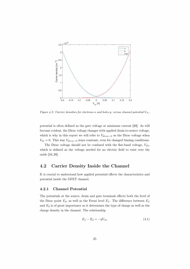
Figure 4.2: Carrier densities for electrons n and holes p, versus channel potential Vch.
potential is often defined as the gate voltage at minimum current [20]. As willbecome evident, the Dirac voltage changes with applied drain-to-source voltage,which is why in this report we will refer to Vdirac−0 as the Dirac voltage whenVds = 0. This way Vdirac−0 stays constant, even for changed biasing conditions.
The Dirac voltage should not be confused with the flat-band voltage, Vfb,which is defined as the voltage needed for no electric field to exist over theoxide [16,20].
4.2 Carrier Density Inside the Channel
It is crucial to understand how applied potential effects the characteristics andpotential inside the GFET channel.
4.2.1 Channel Potential
The potentials at the source, drain and gate terminals effects both the level ofthe Dirac point Ed, as well as the Fermi level Ef . The difference between Efand Ed is of great importance as it determines the type of charge as well as thecharge density in the channel. The relationship
Ef − Ed = −qVch, (4.1)
25

Cox-top
Cox-back
V’gs-top
V’gs-back
Vch
Cq
V
Figure 4.3: Equivalent circuit of GFET electrostatics used to calculate the channelpotential Vch.
is commonly used, where Vch is known as the channel potential. If Vch < 0,then Ef is above Ed, on the contrary if Vch > 0, then Ef is below Ed [15].Vch is discussed and used in many GFET simulations and in modelling, wewill therefore often refer to it instead of Ed and Ef [14–16, 47, 48]. Vch can besubstituted into equations (2.10) and (2.11), hence giving
n =2(kT )2
π(~vF )2F1
(−qVchkT
), (4.2)
p =2(kT )2
π(~vF )2F1
(qVchkT
). (4.3)
Figure 4.2 shows a plot of equations (4.2) and (4.3). In the figure, the effectof the channel potential on the carrier density is clear; for Vch < 0, the carrierdensity of electrons will be the highest, while for Vch > 0 the carrier density forholes will be the highest.
To calculate Vch in GFETs, an equivalent capacitive circuit of the GFET gateelectrostatics can be used, see figure 4.3. Both top- and back-gate potentialsare regulated as
Vgs−top′ = Vgs−top − Vdirac−0−top, (4.4)
Vgs−back′ = Vgs−back − Vdirac−0−back. (4.5)
Vgs−top and Vgs−back are the applied top- and back-gate voltages while Vdirac−0−top
and Vdirac−0−back are the Dirac voltages when Vds = 0 as well as when the re-spective gate voltage is zero. Vgs−back = 0 for Vdirac−0−top and Vgs−top = 0 forVdirac−0−back. [15]. The gate-oxide capacitance for respective top- and back-gate
26
are calculated as
Cox−top =εox−toptox−top
, (4.6)
Cox−back =εox−backtox−back
, (4.7)
where t is the oxide thickness and ε is the oxide permittivity [45]. The exactexpression for the quantum capacitance Cq is [14, 49]
Cq =2q2kT
π(~vF )2ln
(2
(1 + cosh
(qVchkT
))). (4.8)
V in figure 4.3 is the voltage drop between the channel and ground. V getsa relatively simple expression when source is grounded; at the source end thevoltage drop is zero V (x = 0) = 0, while at the drain end the voltage drop it isequal to the drain-to-source voltage V (x = L) = Vds [16].
The expression
Vch = − (Vgs−top′ − V ) · Cox−top + (Vgs−back
′ − V ) · Cox−backCox−top + Cox−back + α(Vch)Cq(Vch)
, (4.9)
can be derived from figure 4.3 [15,45]. The simplified expression
Vch = − (Vgs−top′ − V ) · Cox−top
Cox−top + α(Vch)Cq(Vch), (4.10)
should be used if the device does not have a back-gate terminal [48].
α =kT
qVch·F1
(qVchkT
)− F1
(− qVchkT
)ln(
2(
1 + cosh(qVchkT
))) , (4.11)
is the capacitance weighting factor [15]. It is possible to calculate the value ofVch in both equations (4.9) and (4.10), if the values of V and Vgs are known.
4.2.2 Biasing Configurations
Different biasing configurations are studied in this section, to get a better un-derstanding of the carrier density inside the channel of GFETs. No back-gateis used for the sake of simplicity, and the top-gate is therefore denoted as Vgs.The source is grounded in all configurations. Visual images are used to givea clearer understanding of how the channel looks, but note that the imagesare representative rather than mathematically correct. However, as shown inthe images, the voltage drop in the channel should always be the highest whenthe Fermi energy passes through the Dirac point, as the resistivity there is the
27

S DE
f
Vch
Ed
(a) Scenario A.1.
S D
Ef
Ed
(b) Scenario A.2.
S DE
f
Vch
Ed
(c) Scenario A.3.
Figure 4.4: First instance of scenarios.
highest [45,50].In the first instance, scenarios A.1–A.3, it is assumed that there is no po-
tential difference between source and drain, Vds ≈ 0.
Scenario A.1: Vgs < Vdirac. In this scenario Ef is below Ed, Vch > 0. Fromfigure 4.2, this means that there will be a high concentration of holes. Fordecreased values of Vgs, Ef and Ed move further away from each other, whichincreases the hole concentration and thereby the conductivity in the channel.But, when Vgs is increased, Ef and Ed move closer together, thereby decreasingVch.
Scenario A.2: Vgs = Vdirac. With this applied potential, Ef goes through Ed,Vch = 0. This means that the minimum charge density for electrons and holesis reached, see figure 4.2. The conductivity in the channel is very low.
Scenario A.3: Vgs > Vdirac. In this scenario, Ef is above Ed, Vch < 0. As
28

-1.5 -1 -0.5 0 0.5 1 1.5 2 2.5 3 3.5
Vgs
[V]
-1
-0.8
-0.6
-0.4
-0.2
0
0.2
0.4
0.6
0.8
Vch [
V]
Vds
= 0 V
Vdirac-0
= 0.5 V
Vch
at drain
Vch
at source
O V
Figure 4.5: Channel potential Vch for when the drain-to-source voltage Vds ≈ 0 V andthe Dirac voltage Vdirac−0 = 0.5 V, scenario A.1-A.3.
can be seen in figure 4.2, this means that the electron density is high. AsVgs is increased, Ef and Ed move further apart, decreasing Vch and thereforeincreasing the electron concentration, hence again increasing the conductivityin the channel [16].
Equation (4.10) is used in MATLAB [18] to calculate Vch in scenarios A.1–A.3, the result is displayed in figure 4.5. Vch is calculated at source and drain,since V is only known at these points. The results are in good agreement withthe theory. Vch has the same value at both source and drain, and as expectedVch changes sign at Vgs = Vdirac. The correlating charge densities are alsocalculated at source and drain, see figure 4.6. In the figure it is somewhatdifficult to see all curve values since they overlap. Nevertheless, we can see thatthe results agree with the theory and that same pattern is followed; first highcharge density for holes, which becomes smaller as Vgs increases towards Vdirac.When Vgs > Vdirac electrons dominate the channel, with increasing density forlarger values of Vgs.
Moving on, in the second instance of scenarios, it is assumed that Vds 0
creating a clear potential difference between source and drain. This means thatcharges can flow in the channel.
Scenario B.1: Vgs < Vdirac−0. In this scenario, Ef is below Ed everywherein the channel, Vch > 0. The hole density is high and holes travel from drainto source generating a current in the same direction. Holes are said to be
29

-1.5 -1 -0.5 0 0.5 1 1.5 2 2.5 3 3.5
Vgs
[V]
0
1
2
3
4
5
6
Ca
rrie
r d
en
sity [
cm
-2]
×1013
Vds
= 0 V
Vdirac-0
= 0.5 V
n at drain
p at drain
n at source
p at source
Figure 4.6: Carrier density when the drain-to-source voltage Vds ≈ 0 V and the Diracvoltage Vdirac−0 = 0.5 V, scenario A.1-A.3.
the majority charge carriers. As Vgs increases the difference between Ed andEf decreases, which means the hole density will decrease, which decreases thechannel conductivity and thereby the current.
Scenario B.2: Vgs = Vdirac−0. In this scenario, Ef coincides with Ed at thesource end, Vch = 0. This occurrence is often referred to as the Dirac cone beingintroduced into the channel, see figure 4.7b. Of course, one should note thatthe Dirac cones are not moving into the channel, it is merely an expression. Itwould have been more correct to say that at this occurrence, there is a pointin the channel where Ef and Ed coincide. Ef is below Ed in the rest of thechannel, Vch > 0. Holes are still majority charge carriers for this scenario,but the channel conductivity is lower compared to scenario B.1 [16]. The localchannel resistivity is inversely proportional to the local carrier density, whichmeans that most of the voltage drop occurs at the source side where the localcarrier density is the lowest [50].
Scenario B.3: Vdirac−0 < Vgs < Vdirac−0 + Vds. Increasing the potential fur-ther creates this interesting scenario. Ef is above Ed, Vch < 0, in part of thechannel, while Ef is below Ed, Vch > 0, in the other part of the channel. At theside closest to source, where Vch < 0, there is a high density of free electrons.The potential difference, Vds, will push the electrons from source to drain, con-tributing to the current in the opposite direction. Simultaneously, on the drainside, where Vch > 0, holes will have a higher density and the potential differ-
30
ence will push the holes from drain to source, contributing to the current in thesame direction. Increased gate voltage will decrease the part where Vch > 0,hence decreasing the hole density, this it is often described as the Dirac conemoving further into the channel. When the Dirac cone reaches the middle of thechannel both carrier concentrations are equal. However, the minimum currentwill probably not occur exactly at this point, since the mobility of holes andelectrons often differ.
Scenario B.4: Vgs = Vdirac−0 +Vds. Ef and Ed coincide, Vch = 0, at the drainside and in the rest of the channel Vch < 0. One could say that at this pointthe Dirac cone have moved all the way through the channel from the source tothe drain side.
Scenario B.5: Vgs > Vdirac−0 + Vds. As the voltage continues to increase Efand Ed move away from each other everywhere in the channel, Vch < 0. Theelectron density and the conductivity thereby continue to increase [16].
Calculations are again made with MATLAB [18] for scenarios B.1–B.5. Theresults are displayed in figures 4.8 and 4.9. Figure 4.8 shows that the sourceside is Vch = 0 when Vgs = Vdirac−0, while at drain end is Vch = 0 first atVgs = Vdirac−0 + Vds. As expected, that means that for certain values Vch havedifferent signs throughout the channel, meaning that both electrons and holeswill be charge carriers and thereby contribute to the current. This can also beseen clearly in figure 4.9 where the type of majority charge carriers differs fromsource and drain when Vdirac−0 < Vgs < Vdirac−0 + Vds.
31

S
D
Ef
Vch
Ed
(a) Scenario B.1.
S
D
Ef
Vch
Ed
(b) Scenario B.2.
S
D
Ef
Vch
Ed
(c) Scenario B.3.
S
D
Ef
Vch
Ed
(d) Scenario B.4.
S
D
Ef
Vch
Ed
(e) Scenario B.5.
Figure 4.7: Second instance of scenarios.
32

-1.5 -1 -0.5 0 0.5 1 1.5 2 2.5 3 3.5
Vgs
[V]
-1
-0.8
-0.6
-0.4
-0.2
0
0.2
0.4
0.6
0.8
1
Vch [
V]
Vds
= 1.5 V
Vdirac-0
= 0.5 V
Vch
at drain
Vch
at source
O V
Figure 4.8: Channel potential Vch when the drain-to-source voltage Vds ≈ 1.5 V andthe Dirac voltage Vdirac−0 = 0.5 V, scenarios B.1–B.5.
-1.5 -1 -0.5 0 0.5 1 1.5 2 2.5 3 3.5
Vgs
[V]
0
1
2
3
4
5
6
7
Ca
rrie
r d
en
sity [
cm
-2]
×1013
Vds
= 1.5 V
Vdirac-0
= 0.5 V
n at drain
p at drain
n at source
p at source
Figure 4.9: Carrier density when the drain-to-source voltage Vds ≈ 1.5 V and the Diracvoltage Vdirac−0 = 0.5 V, scenarios B.1–B.5.
For these first two instances of scenarios, A and B, Vds has been constantwhile the value of Vgs has increased. Let us now continue by looking at athird and last instance of scenarios where Vgs is static while Vds changes, here
33
S DE
f
Vch
Ed
(a) Scenario C.1.
S
D
Ef
Vch
Ed
(b) Scenario C.2.
S
D
Ef
Vch
Ed
(c) Scenario C.3.
Figure 4.10: Last instance of scenarios.
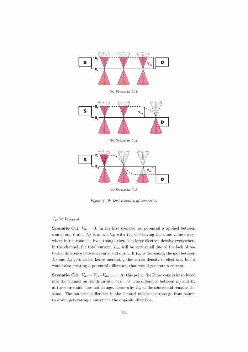
Vgs Vdirac−0.
Scenario C.1: Vds = 0. In the first scenario, no potential is applied betweensource and drain. Ef is above Ed, with Vch < 0 having the same value every-where in the channel. Even though there is a large electron density everywherein the channel, the total current, Ids, will be very small due to the lack of po-tential difference between source and drain. If Vds is decreased, the gap betweenEf and Ed gets wider, hence increasing the carrier density of electrons, but itwould also creating a potential difference, that would generate a current.
Scenario C.2: Vds = Vgs−Vdirac−0. At this point, the Dirac cone is introducedinto the channel on the drain side, Vch = 0. The difference between Ef and Edat the source side does not change, hence why Vch at the source end remains thesame. The potential difference in the channel makes electrons go from sourceto drain, generating a current in the opposite direction.
34

Scenario C.3: Vds > Vgs − Vdirac. Ef is below the Ed, Vch > 0, close to thedrain side. As Vds continues to increase, the Dirac cone moves throughout thechannel. However, since Vch remains constant the source end, the Dirac conecannot move all the way. The channel will have both negative and positive Vch,meaning that both electrons and holes will contribute to the current [16].
-1 -0.5 0 0.5 1 1.5 2 2.5 3
Vds
[V]
-0.8
-0.6
-0.4
-0.2
0
0.2
0.4
0.6
Vch [
V]
Vgs
= 2 V
Vdirac-0
= 0.5 VV
ch at drain
Vch
at source
O V
Figure 4.11: Channel potential Vch when the gate-to-source voltage Vgs = 2.0 V andthe Dirac voltage Vdirac−0 = 0.5 V, scenarios C.1–C.3.
35

-1 -0.5 0 0.5 1 1.5 2 2.5 3
Vds
[V]
0
0.5
1
1.5
2
2.5
3
3.5
4
4.5
Ca
rrie
r d
en
sity [
cm
-2]
×1013
Vgs
= 2 V
Vdirac-0
= 0.5 V
n at drain
p at drain
n at source
p at source
Figure 4.12: Carrier density when the gate-to-source voltage Vgs = 2.0 V and the Diracvoltage Vdirac−0 = 0.5 V, scenarios C.1–C.3.
Final calculations using MATLAB [18] are displayed in figures 4.11 and 4.12.In figure 4.11, the theory of Vch remaining constant at the source end is con-firmed. It is also shown that the potential Vch at the drain end, change sign atVgs = Vgs − Vdirac−0, just like anticipated. In figure 4.12, it can be seen thatboth electrons and holes will contribute to the current for Vds > Vgs−Vdirac−0.
In summary, the most important thing that we can note from this is thatin some scenarios, both electrons and hole contribute to the total current. Inregions where Vch < 0, charge transport will be assured by electrons, and onthe contrary where Vch > 0, holes assume the charge transport role.
When discussing general field-effect transistors (FETs), it is accustomed toexpress the channel as either n-type, when electrons are charge carriers, or p-type, when the charge carriers are holes. That the channel can be adjusted, tobe both n- and p-type, is referred to the transistor as having ambipolar charac-teristics. This is an unusual trait of FETs, since most conventional transistorsare either n- or p-type, not both [8, 9].
4.3 Negative Differential Resistance
An interesting phenomena, that in GFETs is associated with the ambipolartransport, is the negative differential resistance (NDR). The term negative re-sistance refers to when an increased voltage across a device’s terminals results
36

-5 0 5 10 15 20
Vgs-top
[V]
1.2
1.4
1.6
1.8
2
2.2
2.4
2.6
2.8
3
3.2
I ds [
mA
]
Vgs-back
= 7 V
Vdirac-0-top
= 0.5 V
Vdirac-0-back
= 0 V
5 V
5.2 V
5.4 V
5.6 V
5.8 V
6 V
Figure 4.13: Drain-to-source current Ids, versus gate-to-source potential Vgs. Vds =5− 6 V, Vgs−back = 7 V, Vdirac−0−top = 0.5 V and Vdirac−0−back = 0 V.
in a decrease in the electric current. Mathematically NDR can be described as
∆v
∆i< 0, (4.12)
whiledIdsdVds
< 0. (4.13)
is used more specifically for GFETs [9]. Theoretical and experimental resultsshow that NDR occurs in GFETs with all sorts of graphene quality, oxides andgate lengths [9, 38, 50]. It is a general feature of graphene that occurs undercertain biasing conditions [50]. Other devices where NDR can be observedare resonant tunnel diodes, single-electron-transistors and Esaki diodes. Thesedevices have a high peak-to-valley current ratio but they suffer due to low peakcurrent densities. Because of the high current carrying capabilities of GFETs,the devices do not suffer from low peak current densities [38], which is one ofthe main advantages with using GFETs for NDR. Another advantage, is thatit is a three-terminal device, where the gate controls the current flow, whichmeans that the NDR behaviour can be switched on and off.
4.3.1 Theoretical Explanation
In 2012, a group of researchers proposed that the NDR phenomena, in GFETs,occurs as a result of the ambipolar transport [50]. However in 2015, Sharma et
37

2 3 4 5 6 7 8
Vgs-top
[V]
1.2
1.4
1.6
1.8
2
2.2
2.4
2.6
I ds [
mA
]
Vgs-back
= 7 V
Vdirac-0-top
= 0.5 V
Vdirac-0-back
= 0 V
5 V
5.2 V
5.4 V
5.6 V
5.8 V
6 V
Figure 4.14: Enlargment of figure 4.13 showing the drain-to-source current Ids, versusgate-to-source potential Vgs. Vds = 5− 6 V, Vgs−back = 7 V, Vdirac−0−top = 0.5 V andVdirac−0−back = 0 V.
al. showed that the ambipolar transport can only be part of the reason. Thegroup proposed that NDR occurs due to the competition between the carrierdrift velocity and carrier density [38].
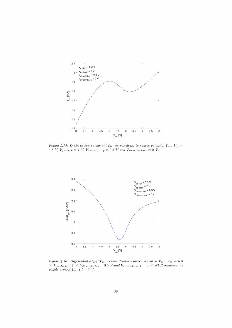
A double-gated GFETmodel is simulated in Advanced Design System (ADS)[17] and displayed using MATLAB [18] in figure 4.13. The simulation modelis described further in Section 5.2.10 Simulation Model 3. Figure 4.13 showsIds versus Vgs−top for six different values of Vds. As can be seen, the point ofminimum current moves to the right for increased potential which leads to anoverlap in the curves around 5 V. The area is enlarged in figure 4.13, between 5
and 6 V it is clear that the simulations with less applied potential Vds, producelarger currents. This means, that for these bias values NDR behaviour shouldbe visible. A new simulation is therefore made with the potential value Vgs−topchosen somewhere in the region where the curves overlap. The simulation resultsare shown in figure 4.15, where NDR is clearly visible.
The value of dIds/dVds is shown in figure 4.16, to more easily observe wherethe negative differential starts and ends. Extracted from the figure, the NDRoccurs around Vds ≈ 5−6 V. To understand the behaviour, the channel potentialVch as well as the carrier densities n and p, are calculated using equations (4.2),(4.3) and (4.9), as in previous scenarios. Figures 4.17 and 4.18 show the resultof the calculations. Ids increases linearly for low values of Vds, however fromfigure 4.18, it can be seen that the electron carrier density decreases with in-
38
3 3.5 4 4.5 5 5.5 6 6.5 7 7.5 8
Vds
[V]
1.4
1.5
1.6
1.7
1.8
1.9
2
2.1
I ds [
mA
]V
gs-top = 5.3 V
Vgs-back
= 7 V
Vdirac-0-top
= 0.5 V
Vdirac-0-back
= 0 V
Figure 4.15: Drain-to-source current Ids, versus drain-to-source potential Vds. Vgs =5.3 V, Vgs−back = 7 V, Vdirac−0−top = 0.5 V and Vdirac−0−back = 0 V.
3 3.5 4 4.5 5 5.5 6 6.5 7 7.5 8
Vds
[V]
-0.2
-0.1
0
0.1
0.2
0.3
0.4
diff(
I ds)
[mA
/V]
Vgs-top
= 5.3 V
Vgs-back
= 7 V
Vdirac-0-top
= 0.5 V
Vdirac-0-back
= 0 V
Figure 4.16: Differential dIds/dVgs, versus drain-to-source potential Vds. Vgs = 5.3V, Vgs−back = 7 V, Vdirac−0−top = 0.5 V and Vdirac−0−back = 0 V. NDR behaviour isvisible around Vds ≈ 5− 6 V.
39

3 3.5 4 4.5 5 5.5 6 6.5 7 7.5 8
Vds
[V]
-1.5
-1
-0.5
0
0.5
1V
ch [
V]
Vgs-top
= 5.3 V
Vgs-back
= 7 V
Vdirac-0-top
= 0.5 V
Vdirac-0-back
= 0 V
Vch
at drain
Vch
at source
O V
Figure 4.17: Channel potential Vch, versus applied drain-to-source potential Vds. Vgs =5.3 V, Vgs−back = 7 V, Vdirac−0−top = 0.5 V and Vdirac−0−back = 0 V.
3 3.5 4 4.5 5 5.5 6 6.5 7 7.5 8
Vds
[V]
0
5
10
15
Ca
rrie
r d
en
sity [
cm
-2]
×1013
Vgs-top
= 5.3 V
Vgs-back
= 7 V
Vdirac-0-top
= 0.5 V
Vdirac-0-back
= 0 V
n at drain
p at drain
n at source
p at source
Figure 4.18: Charge densities n and p, versus channel potential Vch. Vgs = 5.3 V,Vgs−back = 7 V, Vdirac−0−top = 0.5 V and Vdirac−0−back = 0 V.
40

creased Vds. The current continues to grow because a greater potential leadsto an increased drift velocity. The drift velocity continues to increase until itreaches the velocity saturation, which is inversely proportional to the squareroot of the total carrier density. This means that the velocity saturation is highfor low carrier densities, while the velocity saturates at lower values for highcarrier densities [45].
If NDR is wanted in a GFET, it is important to know about the physicsbehind the phenomena as it will help when choosing biasing conditions. ForNDR to be visible an increase in the potential Vds needs to lead to a decreasein carrier density. However, the total carrier density should be large enoughto cause velocity saturation [45], otherwise no NDR will be visible. This oftenmeans applying large gate potentials, which has been done in this simulationexample.
41

Chapter 5
Modelling GrapheneField-Effect Transistor
In this chapter, different simulation models for graphene field-effect transistors(GFETs) are investigated further. All models must be compatible with thehardware description language Verilog-A. This means that we are restricted tothe models that we can solve analytically, since the program cannot solve equa-tions numerically. However, equations are solved numerically in MATLAB [18],to compare and validate calculations as well as approximations before imple-mentation. The full models are run using the simulation program AdvancedDesign System (ADS) [17].
The general current expression for GFETs can be written as
Ids = −WQ(x)vdrift(x), (5.1)
where W is the width of the channel, Q is the charge carrier density and vdriftis the drift velocity of the carriers [14,16,45,51]. The assumptions, calculationsand approximations made to 5.1 will determine the accuracy of the model.
This chapter contains four different simulation models, all of which havebeen implemented in Verilog-A and run with ADS [17]. All models have beenexplained and most calculations are shown explicitly. The chapter begins withSection 5.1 Ballistic Transport that clarifies how transistor length effects whatmodel that can be used. Section 5.2 Drift-Diffusion Model compares differentparameter approximations for the drift-diffusion (DD) model, all calculationsand graphs are displayed using MATLAB [18]. Finally, Section 5.3 VirtualSource Model gives a short introduction into the virtual source (VS) model.
42
5.1 Ballistic Transport
The basic concept of local equilibrium have been discussed in Section 2.4 LocalEquilibrium. The assumption of local equilibrium in GFETs is based on thefact that electrons scatter and collide inside the channel. The average lengtheach electron travels before a scattering event is called the mean free path λ
[25]. When the channel length becomes smaller, going towards λ, the carriersstart travelling without experiencing any collisions or scatterings that impedetheir motion. This type of transport is called ballistic transport. When noscattering or collisions occur, the assumption of local equilibrium is no longervalid. Therefore no (quasi-)Fermi levels can be defined, which is one of thereasons why modelling of ballistic semiconductors is more complicated [52]. Themean free path for graphene, see table 2.1, is relatively long which means thatballistic transport cannot be ignored even for transistors that normally are seenas long channel devices. Additionally, ballistic behaviour for GFETs has beendetected for device lengths longer than 10 µm [3].
5.1.1 Quasi-Ballistic Transport
In literature, the common way to denote quasi-ballistic transport, is any devicein which ballisticity can be detected to such degree that it cannot be neglected,irrespectively of the channel length [25, 53]. In quasi-ballistic devices, high en-ergy carriers travel ballistically while other particles travel diffusively. Thismeans that a model for quasi-ballistic transport has to consider both collision-free and collision-dominated transport [53].
One interesting point in quasi-ballistic transport models is that quasi Fermilevels cannot be determined. This makes the carrier mobility a questionableconcept from a theoretical standpoint. Nevertheless, the mobility can still bemeasured practically even in the smallest devices [54].
5.2 Drift-Diffusion Model
The drift-diffusion (DD) model is commonly used in literature as well as sci-entific reports. The model is made under the assumption of local equilibrium.Local equilibrium enables calculations of local quasi-Fermi levels, from which thecarrier distribution can be calculated using Fermi-Dirac statistics [25]. However,because local equilibrium must be established, the DD model have a distinctrestriction; the model can only be used on GFETs with channel length longerthan the mean free path λ [14].
43

5.2.1 Drift Velocity and New Current Expression
To calculate the current of the model we firstly focus on the last part of equa-tion (5.1), the drift velocity vdrift. The drift velocity can be written as
vdrift =µE
1 + µ|E|vsat
=µ(−dVdx )
1 +µ|− dVdx |vsat
, (5.2)
where µ is the mobility, V is the potential in the channel compared to ground,and vsat is the saturation velocity [15, 45]. Substituting the expression fromequation (5.2) into equation (5.1) gives
Ids = −WQ(x)µ(−dVdx
)1 +
µ|− dVdx |vsat
. (5.3)
Upon first glance, the expression seems daunting, but after some re-arrangementand calculations,
Ids
(1 +
µ|dVdx |vsat
)= WQ(x)µ
(dV
dx
),
L∫0
Ids
(1 +
µ|dVdx |vsat
)dx =
L∫0
WQ(x)µ
(dV
dx
)dx,
Ids
L+
L∫0
µ|dVdx |vsat
dx
= W
L∫0
Q(x)µ
(dV
dx
)dx,
Ids
L+
∣∣∣∣∣∣Vds∫0
µ
vsatdV
∣∣∣∣∣∣ = W
Vds∫0
Q(x)µdV,
(5.4)
a relatively simple form,
Ids = W
Vds∫0
Q(x)µdV
L+
∣∣∣∣∣Vds∫0 µvsat
dV
∣∣∣∣∣, (5.5)
can be found. The dilemma with equation (5.5) is that the integral is overV , instead of the preferable Vch, which most of our variables have a knowndependency on. Because the relationship between V and Vch is well knownfrom equation (4.9), the following replacement
dV = dVdVchdVch
= dVchdV
dVch, (5.6)
44
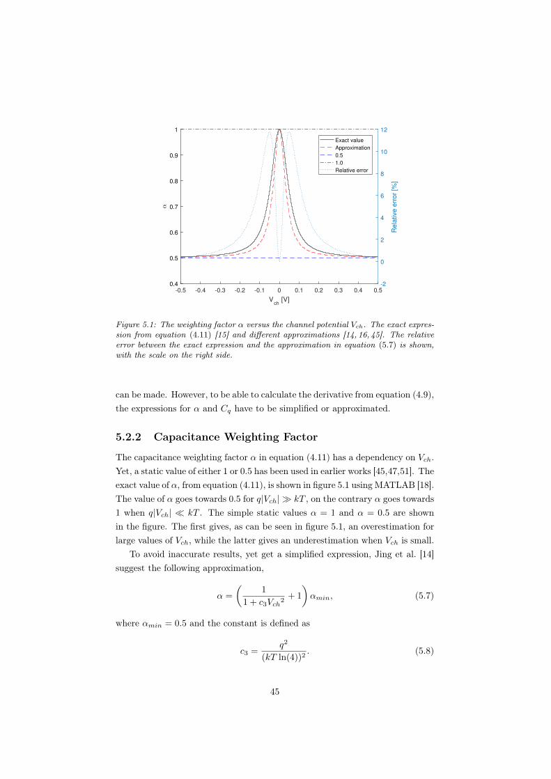
-0.5 -0.4 -0.3 -0.2 -0.1 0 0.1 0.2 0.3 0.4 0.5
Vch
[V]
0.4
0.5
0.6
0.7
0.8
0.9
1
α
-2
0
2
4
6
8
10
12
Re
lative
err
or
[%]
Exact value
Approximation
0.5
1.0
Relative error
Figure 5.1: The weighting factor α versus the channel potential Vch. The exact expres-sion from equation (4.11) [15] and different approximations [14, 16, 45]. The relativeerror between the exact expression and the approximation in equation (5.7) is shown,with the scale on the right side.
can be made. However, to be able to calculate the derivative from equation (4.9),the expressions for α and Cq have to be simplified or approximated.
5.2.2 Capacitance Weighting Factor
The capacitance weighting factor α in equation (4.11) has a dependency on Vch.Yet, a static value of either 1 or 0.5 has been used in earlier works [45,47,51]. Theexact value of α, from equation (4.11), is shown in figure 5.1 using MATLAB [18].The value of α goes towards 0.5 for q|Vch| kT , on the contrary α goes towards1 when q|Vch| kT . The simple static values α = 1 and α = 0.5 are shownin the figure. The first gives, as can be seen in figure 5.1, an overestimation forlarge values of Vch, while the latter gives an underestimation when Vch is small.
To avoid inaccurate results, yet get a simplified expression, Jing et al. [14]suggest the following approximation,
α =
(1
1 + c3Vch2+ 1
)αmin, (5.7)
where αmin = 0.5 and the constant is defined as
c3 =q2
(kT ln(4))2. (5.8)
45

Using MATLAB [18], the relative error, between equation (5.7) and equa-tion (4.11), is calculated. The biggest error occurs when Ef and Ed are inclose proximity of each other, with maximum value of 11.78% . The relativeerror becomes almost undistinguishable for large values of |Vch|.
5.2.3 Quantum Capacitance
Because of the complexity of equation (4.8) approximations are commonly ac-cepted. Two different approximations as well as the exact value are shown infigure 5.2. A very simple approximation expressed as
Cq = 2qc4|Vch| (5.9)
can be used [47], where the constant c4 is defined as
c4 =q2
π(~vF )2. (5.10)
However, the approximation in equation (5.9) is inaccurate in the proximity ofVch = 0. Another approximation, commonly known as the square-root-basedapproximation,
Cq =2q2kT ln(4)
π(~vF )2
√1 +
(qVch
kT ln(4)
)2
, (5.11)
can be used to improve the accuracy [51]. The relative error, between thesquare-root approximation and the exact result, is calculated and displayedwith MATLAB [18], the maximum relative error is 7.97%.
5.2.4 dV/dVch
The derivative of equation (4.9) can be written in a simple form if one assumesthat capacitance weighting factor α = 1 and if one ignores the fact that thequantum capacitance Cq depends on Vch. This gives the expression
dV
dVch= 1 +
Cq(Vch)
Cox−top + Cox−back. (5.12)
If one instead uses equation (5.7) for α and the square-root approximation inequation (4.8) for Cq substituted into equation (4.9), the derivative can beexpressed as
dV
dVch= 1 +
c5αmin(2 + c3Vch
2(3 + 2c3Vch
2))
(1 + c3Vch2)32
. (5.13)
46

-0.2 -0.15 -0.1 -0.05 0 0.05 0.1 0.15 0.2
Vch
[V]
0
5
10
15
20
25
30
35
40
45
50
Ca
pa
cita
nce
[µ
F/c
m2]
-8
-7
-6
-5
-4
-3
-2
-1
0
Re
lative
err
or
[%]
Exact model
Square-root approximation
Other approximation
Relative error
Figure 5.2: Quantum capacitance Cq. Exact value, square-root approximation [51] aswell as a second approximation [16]. The relative error between the exact expressionin equation (4.8) and the approximation in equation (5.11) is shown, with the scale onthe right side.
-0.2 -0.15 -0.1 -0.05 0 0.05 0.1 0.15 0.2
Vch
[V]
2
3
4
5
6
7
8
9
10
dV
/dV
ch
-5
-4
-3
-2
-1
0
1
Re
lative
diffe
ren
ce
[%
]
Approximation 1
Approximation 2
Relative difference
Figure 5.3: Two approximations for dV/dVch. Approximation 1 corresponds to equa-tion (5.12), while Approximation 2 corresponds to equation (5.13). The relative dif-ference is shown, with the scale on the right side.
47

Where the definition of c3 is shown in equation (5.8) and c5 is defined as
c5 =2q2kT ln(4)
(Cox−top + Cox−back)π(~vF )2. (5.14)
Equations (4.6) and (4.7) show further details about Cox−top and Cox−back.A comparison of the two approximations for dV/dVch from equations (5.12)and (5.13) are shown in figure 5.3. The figure shows that the biggest differenceoccurs in the vicinity of Vch = 0, with maximum value -4.7%.
5.2.5 Carrier Density
There are three important parameters that have not been discussed yet: Q(x),µ and vsat. The net mobile sheet charge density Qnet can be used as the chargecarrier density, and is expressed as
Qnet = |q(p− n)|. (5.15)
Equation (5.15) is useful for conventional field-effect transistors (FETs). How-ever, this approximation underestimates the carrier density for when Ef andEd are in close proximity, because holes and electrons in graphene both addi-tively contribute to the overall current, as discussed in Section 4.2.2 BiasingConfigurations. Accurate result is therefore only given from equation (5.15)when q|Vch| kT . The charge density relevant for transport,
Qt = q(p+ n), (5.16)
can be used as a mean to improve the model [51]. Equation (5.16) goes towardsequation (5.15) when q|Vch| kT , but gives a better approximation for smallvalues of Vch. Figure 5.4 shows a comparison of equations (5.15) and (5.16).
Using the exact expression for Qt demands calculations of n and p with theFermi-Dirac integral, which is not completely trivial. A simplification proposedby Parrish et al. [51] can be written as
Qt ≈qπ(kT )2
3(~vF )2+
q3Vch2
π(~vF )2, (5.17)
and will be used in this report. The simplification shows good agreement withthe exact data, see figure 5.5. The maximum relative error is only 0.0001%.
Another constant is introduced, to simplify for later calculations:
c6 =π(kT )2
3(~vF )2, (5.18)
48
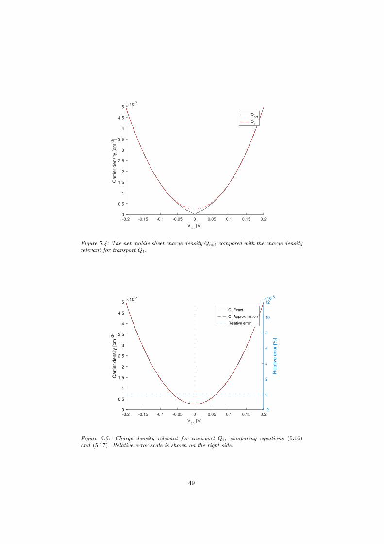
-0.2 -0.15 -0.1 -0.05 0 0.05 0.1 0.15 0.2
Vch
[V]
0
0.5
1
1.5
2
2.5
3
3.5
4
4.5
5
Ca
rrie
r d
en
sity [
cm
-2]
×10-7
Qnet
Qt
Figure 5.4: The net mobile sheet charge density Qnet compared with the charge densityrelevant for transport Qt.
-0.2 -0.15 -0.1 -0.05 0 0.05 0.1 0.15 0.2
Vch
[V]
0
0.5
1
1.5
2
2.5
3
3.5
4
4.5
5
Ca
rrie
r d
en
sity [
cm
-2]
×10-7
-2
0
2
4
6
8
10
12
Re
lative
err
or
[%]
×10-5
Qt Exact
Qt Approximation
Relative error
Figure 5.5: Charge density relevant for transport Qt, comparing equations (5.16)and (5.17). Relative error scale is shown on the right side.
49

-0.2 -0.15 -0.1 -0.05 0 0.05 0.1 0.15 0.2
Vch
[V]
0
1
2
3
4
5
6
Ca
rrie
r d
en
sity [
cm
-2]
×10-7
Qt without n
pud
Qtot
with npud
Figure 5.6: Comparison between the Qt and Qtot from equations (5.19) and (5.21).
Together with c4 in equation (5.10) this gives the very short expression
Qt = q(c6 + c4Vch2). (5.19)
Finally, the residual charge density known as electron-hole puddles,
npud =∆2
π(~vF )2(5.20)
where ∆ is the spatial inhomogeneity of potential resulting in the puddles [15],has to be added to the expression. This gives
Qtot = q(c6 + c4Vch2 + npud). (5.21)
5.2.6 Mobility
The second undefined parameter, is the mobility µ. The effective carrier mobilityµeff is defined as
µeff =nµn + pµp + npud
(µn+µp
2
)n+ p+ npud
, (5.22)
where µn and µp are the low field mobilities for electrons and holes. However,the fact that the mobility decreases with increased carrier density also has to
50

-1 -0.8 -0.6 -0.4 -0.2 0 0.2 0.4 0.6 0.8 1
Vch
[V]
400
500
600
700
800
900
1000
1100
1200
1300
Mo
bili
ty [
cm
2/(
Vs)]
Definition
Approximation 1
Approximation 2
Figure 5.7: Comparison between different approximations for the effective mobilityµeff . The definition from equation (5.22) is shown in comparison with Approxima-tion 1 from equation (5.23) [14] as well as the more practical Approximation 2 fromequation (5.25) [55].
-0.2 -0.15 -0.1 -0.05 0 0.05 0.1 0.15 0.2
Vch
[V]
950
1000
1050
1100
1150
1200
1250
1300
Mo
bili
ty [
cm
2/(
Vs)]
-1
-0.8
-0.6
-0.4
-0.2
0
0.2
0.4
0.6
0.8
Re
lative
diffe
ren
ce
[%
]
Definition
Approximation 1
Approximation 2
Relative difference
Figure 5.8: Enlargment of figure 5.7, comparing different approximations for the effec-tive mobility µeff . The definition from equation (5.22) is shown in comparison withApproximation 1 from equation (5.23) [14] as well as the more practical Approxima-tion 2 from equation (5.25) [55]. The relative difference between Approximation 1 and2 is shown, with the scale on the right side
51

be taken into consideration. An added factor such as
µeff =nµn + pµp + npud
(µn+µp
2
)n+ p+ npud
(s
s+ Vch2
), (5.23)
give better agreement with reality [55]. s is in the unit the square of the referencechannel potential, used as an empirical fitting parameter. Once again, we wantto avoid complicated calculations and instead have a dependency on Vch, asthis will help us for future calculations. A simplification for µnp is suggested byDorgan et al. [55] and can be written as follows
µnp =
(14(µp − µn)Vch√
1 + c3Vch2+µp + µn
2
). (5.24)
Together with the approximated expression for (n+ p), in equation (5.19), theexpression
µeff =
(14(µp − µn)(c6 + c4Vch
2)Vch
(c6 + c4Vch2 + npud)√
1 + c3Vch2+µp + µn
2
)(s
s+ Vch2
)(5.25)
is derived. The constants are defined in equations (5.8), (5.10) and (5.18).The expressions for mobility in equations (5.22), (5.23) and (5.25) are shown infigures 5.7 and 5.8. The relative difference between equations (5.23) and (5.25)is also shown. The biggest difference occurs in the proximity of Vch = 0 withthe value 0.9% .
5.2.7 Velocity Saturation
Finally the third variable, vsat is reviewed. Velocity saturation is assumed tobe caused by scattering of phonons, once the carrier reaches a specific energythreshold, it will immediately scatter [56]. In some literature [16, 47], vsat hasbeen modelled as being constant, for example as
vsat =2vFπ. (5.26)
However, the velocity saturation changes with Vch, as we know from Section 4.3Negative Differential Resistance. Therefore, other approximations of vsat haveto be used to accurately represent this dependency. To model vsat as beinginversely proportional to Vch has been fairly popular. A fitting parameter isoften added to improve the accuracy of the model [16, 51, 56]. One simple
52

-0.2 -0.15 -0.1 -0.05 0 0.05 0.1 0.15 0.2
Vch
[V]
0
0.1
0.2
0.3
0.4
0.5
0.6
0.7
0.8
0.9
1
vsa
t/vf
-6
-4
-2
0
2
4
6
8
Re
lative
diffe
ren
ce
[%
]
Constant
Approximation 1
Approximation 2
Approximation 3
Relative difference
Figure 5.9: Four approximations for vsat. The constant approximation correspondsto equation (5.26) [16], Approximation 1 corresponds to equation (5.27) [16, 51, 56],Approximation 2 corresponds to equation (5.28) [15, 57] and finally the continuousfunction in Approximation 3 corresponds to equation (5.29) [14]. The relative differ-ence between Approximation 2 and 3 is shown, with the scale on the right side.
example, without a fitting parameter, is
vsat =~Ω
~√
πQnetq
, (5.27)
where ~Ω is the optical phonon energy [16, 51, 56]. Equation (5.27) providesgood results for high values of |Vch|, but goes to infinity as Vch goes towardszero, giving unrealistic values. A two-region model such as,
vsat =
2qΩ
π2~vFQnet
√πQnet(~vF )2
q −(~Ω
2
)2, when |Qnet| ≥ q Ω2
2πvF 2 ,
2vFπ , when |Qnet| < q Ω2
2πvF 2 ,(5.28)
can be used to avoid the inaccuracy in the proximity of Vch = 0 [15,57]. However,a two-region model is not optimal since it causes problems, for example by givingdiscontinuities in gm. A continuous model that does not go to infinity would beoptimal. The approximation
vsat = vF
(vsat(max)−vsat(min)
vF
1 + c7Vch2+vsat(min)
vF
), (5.29)
53

0 0.5 1 1.5
Vds
[V]
0
20
40
60
80
100
120
140
160
I ds [µ
A/µ
m]
Vgs-top
= -1 V
Vgs-top
= 0 V
Vgs-top
= 1 V
Vgs-top
= 2 V
Figure 5.10: Drain-to-source current Ids versus drain-to-source potential Vds shownfor both measured data provided by Wang et al. [32] and DD model derived from equa-tion (5.33).
wherec7 =
( q
5kT
)2
, (5.30)
gives reasonable results with a continuous function [14]. Figure 5.9 shows acomparison between the approximations. The relative difference between equa-tions (5.28) and (5.29) is visible with the scale on the right side. The differenceis biggest when Ed and Ef are in close proximity with each other, with themaximum difference 6.84%.
5.2.8 Simulation Model 1
My first simulation model begins with the expression described in equation (5.5).The model assumes that the mobility is not dependent on the potential, in thesame manner as has been done by Jiménez [47]. Furthermore, vsat is also saidto be independent on the potential, as in equation (5.26). This means that theexpression can be simplified
Ids =
µWVds∫0
Q(x)dV
L+ µπ|Vds|2vF
. (5.31)
54
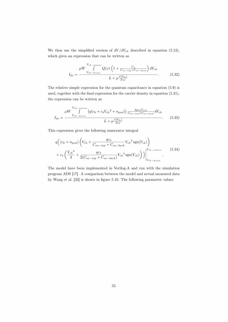
We then use the simplified version of dV /dVch described in equation (5.12),which gives an expression that can be written as
Ids =
µWVch−source∫Vch−drain
Q(x)(
1 +Cq
Cox−top+Cox−back
)dVch
L+ µπ|Vds|2vF
. (5.32)
The relative simple expression for the quantum capacitance in equation (5.9) isused, together with the final expression for the carrier density in equation (5.21),the expression can be written as
Ids =
µWVch−source∫Vch−drain
(q(c6 + c4Vch
2 + npud)) 2qc4|Vch|Cox−top+Cox−back
dVch
L+ µπ|Vds|2vF
. (5.33)
This expression gives the following numerator integral
q(
(c6 + npud)
(Vch +
qc4Cox−top + Cox−back
Vch2 sgn(Vch)
)
+ c4
(Vch
3
3+
qc42(Cox−top + Cox−back)
Vch4 sgn(Vch)
))∣∣∣∣∣Vch−source
Vch−drain
.
(5.34)
The model have been implemented in Verilog-A and run with the simulationprogram ADS [17]. A comparison between the model and actual measured databy Wang et al. [32] is shown in figure 5.10. The following parameter values
55
L = 5 µm, (5.35)
W = 1 µm, (5.36)
tox−top = 15 nm, (5.37)
tox−back = 300 nm, (5.38)
εox−top = 8.9, (5.39)
εox−back = 3.9, (5.40)
Vgs−back = 0 V, (5.41)
Vdirac−0−top = 1.1 V, (5.42)
Vdirac−0−back = 11 V, (5.43)
Rsource = 2 mΩ, (5.44)
Rdrain = 2 mΩ, (5.45)
µn = 920 cm2/(Vs), (5.46)
µp = 1330 cm2/(Vs), (5.47)
∆ = 0.092 V2, (5.48)
are used in the simulation, all of which are extracted from the measured databy Wang et al. [32]. Vgs−top have four different values; -1,0,1 and 2 V as shownin the figure. The mobility is assumed to be constant in this simple simulationmodel and is taken as a average between the hole and electron mobility.
5.2.9 Simulation Model 2
In this simulation model we start by making the same assumptions as in Sec-tion 5.2.8 Simulation Model 1; the mobility µ is independent of the potential,the velocity saturation vsat is said to be constant as in equation (5.26) anddV /dVch is described by equation (5.12). This gives us the same expression asin equation (5.32). However, moving forward we use the more accurate square-root approximation in equation (5.11) for the quantum capacitance Cq. Thefollowing expression is obtained
Ids =
µWVch−source∫Vch−drain
Q(x)
1 +
2q2kT ln(4)
π(~vF )2
√1+(
qVchkT ln(4)
)2
Cox−top+Cox−back
dVch
L+ µ
∣∣∣∣∣Vds∫0 1vsat(Vch)dV
∣∣∣∣∣. (5.49)
56

0 0.5 1 1.5
Vds
[V]
0
20
40
60
80
100
120
140
160
I ds [µ
A/µ
m]
Vgs-top
= -1 V
Vgs-top
= 0 V
Vgs-top
= 1 V
Vgs-top
= 2 V
Figure 5.11: Drain-to-source current Ids versus drain-to-source potential Vds shownfor both measured data provided by Wang et al. [32] and DD model derived from equa-tion (5.49).
The numerator integral can then be calculated analytically, which gives
qc43Vch
3 − c88(c3)3/2
arcsinh (√c3Vch)
+√
1 + c3Vch2
(c88c3
Vch +c84Vch
3
)∣∣∣∣∣Vch−source
Vch−drain
+ q (c6 + npud)Vds
(5.50)where the constants are defined as equations (5.8), (5.10) and (5.18) as well as
c8 =1
Cox−top + Cox−back· 2q5kT ln(4)
π2(~vF )4. (5.51)
The model is implemented in Verilog-A and run using the simulation pro-gram ADS [17]. The same parameter values as in Section 5.2.8 SimulationModel 1, equations (5.35)–(5.48) are used, with the result shown in figure 5.11.
5.2.10 Simulation Model 3
In this section we derive a simulation model that uses the most the more pre-cise approximations described in previous sections. The mobility is thereforenot assumed to be independent of the potential, but instead as described in
57

0 0.5 1 1.5
Vds
[V]
0
20
40
60
80
100
120
140
160
I ds [µ
A/µ
m]
Vgs-top
= -1 V
Vgs-top
= 0 V
Vgs-top
= 1 V
Vgs-top
= 2 V
Figure 5.12: Drain-to-source current Ids versus drain-to-source potential Vds shownfor both measured data provided by Wang et al. [32] and DD model derived from equa-tions (5.53) and (5.54).
equation (5.25). Equation (5.13) is substituted into equation (5.5) which gives
Ids = W
Vch−source∫Vch−drain
Qµ
(1 +
c5αmin(2+c3Vch2(3+2c3Vch
2))(1+c4Vch2)
32
)dVch
L+
∣∣∣∣∣Vch−source∫Vch−drain
µvsat
(1 + c5αmin(2+c3Vch2(3+2c3Vch2))
(1+c4Vch2)32
)dVch
∣∣∣∣∣. (5.52)
Substituting equations (5.21), (5.25) and (5.29) into equation (5.52) gives anexpression, with the numerator
W
Vch−source∫Vch−drain
(q(c6 + c4Vch
2 + npud))
·(
14(µp − µn)(c6 + c4Vch2)Vch
(c6 + c4Vch2 + npud)√
1 + c3Vch2+µp + µn
2
)(s
s+ Vch2
)·
(1 +
c5αmin(2 + c3Vch
2(3 + 2c3Vch
2))
(1 + c4Vch2)32
)dVch.
(5.53)
58

and the denominator
L+
∣∣∣∣∣∣∣∣Vch−source∫Vch−drain
(14(µp−µn)(c6+c4Vch
2)Vch
(c6+c4Vch2+npud)√
1+c3Vch2+
µp+µn2
)(s
s+Vch2
)vF
(vsat(max)−vsat(min)
vF
1+c7Vch2 + vsat(min)vF
)∣∣∣∣∣∣∣∣
·
∣∣∣∣∣(
1 +c5αmin
(2 + c3Vch
2(3 + 2c3Vch
2))
(1 + c4Vch2)32
)dVch
∣∣∣∣∣ .(5.54)
To simplify the calculation of the expression we assume is assumed that Vch fornpud is the average value of Vch−drain and Vch−source, the same approximationhas been made by Jing et al. [14]. The expression is solved analytically andimplemented in Verilog-A. A simulation is made using ADS [17]. Figure 5.12shows a comparison between measured data, from Wang et al. [32], and thesimulated DD model from equations (5.53) and (5.54). The same parametervalues as in Section 5.2.8 Simulation Model 1, equations (5.35)–(5.48) are used.
5.3 Virtual Source Model
The model described in this section focuses on ballistic transport and is there-fore applicable for shorter channels where the ballistic transport is dominant.However, adjustments can be made to the model so that it works also in thediffusive regime.
The VS model is an alternative transport model based on the concept of one(or several) virtual source(s). The height of the VS modulates the number ofcharge carriers injected. All carriers that exceed the potential of the VS are saidto travel ballistically to the other terminal with a drift velocity in accordancewith the potential difference between source and drain Vds [4, 25,32].
For graphene this means that a positive drain-to-source potential Vds willcreate an electric field that makes holes travel from drain to source, while elec-trons will travel from source to drain. According to the VS model, the electronsthat are injected from the source with energies higher than the VS at source,travel ballistically through the channel to the drain side. Simultaneously, holesinjected from the drain side, with energies lower than the VS at source, willtravel ballistically to the source side. Both electrons and holes contribute to thedrain-to-source current Ids. The carriers that cannot pass the barrier on theirrespective side are reflected back [4, 48,52].
The principle for ballistic transport starts off the same way as any other longchannel GFETs. The gate voltages electrostatics controls the charge density atthe virtual sources. The concentrations at the virtual sources can be calculated
59
as [4, 32,48]
QV S−elec = Cox−topc9φt ln
(1 + e
Vgs−Vt−elecc9φt
)+Qdis, (5.55)
QV S−hole = Cox−topc9φt ln
(1 + e
Vgs+Vt−holec9φt
)+Qdis, , (5.56)
where Vt−elec and Vt−hole can be found by solving
Vt−elec = Vdirac−0−top − c10φt1
1 + e
Vgs−(Vt−elec− c10φt2 )c10φt
2
, (5.57)
Vt−hole = Vdirac−0−top − c10φt1
1 + e
Vgs+(Vt−hole+ c10φt2 )c10φt
2
.. (5.58)
Some clarification regarding the notations are in order; Qdis is the charge densityas a result of electron-hole puddles, both c10 and c9 are related to the sub-threshold, and φt is the thermal voltage defined as
φt =kT
q. (5.59)
Qdis, c9, c10 and the oxide thickness tox−top are fitting parameters that have tobe adjusted to experimental data or numerical calculations, for each simulation[32,48].
Calculation of the drift velocity can be done in a similar manner as for theDD model. Rakheja et al. [48] presents the following equation
vdrift =Vdsµ
L
(1 +
(Vdsvsat
)β) 1β
,
=Vdsµ
L
(1 +
(VdsµvV S0L
)β) 1β
(5.60)
The expression is presented in a different manner but contains the same com-ponents; a dependency on the mobility µ and the velocity saturation vsat. L isthe length of the transistor channel, vV S0 is the carrier injection velocity at thevirtual source and β is a fitting parameter. The injection velocity and mobilityare the same for both holes and electrons [48]. Instead a contact resistancesare used as a means to compensate for the different behaviours in the hole andelectron branch. Rhole < Relec for when the hole transport is larger [4].
What is interesting with this approximation is that the final current expres-
60

sionIds = W (QV S−elec +QV S−hole)vdrift, (5.61)
can be found in a relatively simple manner.
5.3.1 Simulation Model 4
The final simulation model is implemented in Verilog-A and run using ADS [17].The parameters used are taken from Rakheja et al. [48] or the parameter isassumed to be the same as for the other simulations.
0 0.5 1 1.5
Vds
[V]
0
200
400
600
800
1000
1200
1400
1600
I ds [µ
A/µ
m]
Vgs-top
= -1 V
Vgs-top
= 0 V
Vgs-top
= 1 V
Vgs-top
= 2 V
Figure 5.13: Drain-to-source current Ids versus drain-to-source potential Vds shownfor both measured data provided by Rakheja et al. [48] and VS model derived fromequation (5.61).
61

Chapter 6
Discussion of Result
I realised, already at the beginning of my thesis work, that there was a lack offundamental explanations for the advanced simulation models used for graphenefield-effect transistors (GFETs). Graphene and GFETs are relatively new fields,so it is not peculiar that there is room for improvement and that the educationalmaterial is sparse at some levels.
Simultaneously, researchers try to push the limits and be first in discoveringthe next revolutionary step for graphene. This means that there is an abundanceof advanced articles to read, but not much that cover the fundamentals. I wantto note that we cannot expect articles to explain every detail as most publisherhave strict length limits. But I still find it rather discouraging that the reader isassumed to have a deep understanding of not only electronics, but also physics,quantum mechanics, mathematics and fabrication processes. That is why Idecided to put a large emphasis on the theory behind GFETs, maybe it couldmake more people discover the interesting fields of graphene and GFETs.
If the fundamental knowledge is missing, I experienced that it is demandingto understand why some simulation models are more or less accurate. Thatevery author seems to claim that their model is as accurate as it can get doesnot make it any easier. On several occasions, [14–16, 32, 47, 53] authors useanother person’s findings together with their own improvements. However, Ihave from time to time encountered articles where it seems like the author hasnot fully understood the theory from the previous author, on which they arenow building their model.
Furthermore, if a basic understanding is missing, notations and terms canget lost and mixed together, which means that two simulation models can havethe same terms, yet mean different things. For example, Rakheja et al. [48]present a simulation model that has the parameter Qdis. This parameter is saidto describe the electron-hole puddles, which has been denoted as npud in other
62

-1 -0.8 -0.6 -0.4 -0.2 0 0.2 0.4 0.6 0.8 1
Vgs
[V]
2.5
3
3.5
4
4.5
5
5.5
6
6.5
Qx0 [
cm
2]
×10-7
-0.5
0
0.5
1
1.5
2
2.5
3
Re
lative
err
or
[%]
Qx0e
+ Qx0h
Definition
Qx0e
+ Qx0h
Appr 1
Relative error
Figure 6.1: Comparison between the charge density QV S−elec and QV S−hole from equa-tions (5.55) and (5.56) [48], and the charge density in equations (4.2) and (4.3).
simulation models [15, 16]. However, in the former model the parameter is alsoused as a fitting parameter, which means that it has to be adjusted. For me,that is something that is likely to create confusion.
When I started my thesis work, my first choice was to look at the virtualsource (VS) model since it works even in the ballistic regime. However, themodel did not succeed in showing negative differential resistance (NDR). Thenext question therefore became why did it not showcase NDR. As describedin this report, the theory behind NDR has been under debate and differenttheories have been put forward. Again, I felt like the fundamental knowledgewas missing. I therefore decided to not only research the theory behind grapheneand GFETs, but also to look at the more commonly used drift-diffusion (DD)model that I know manages to showcase NDR.
Comparing the VS model with the DD model is complicated. A simplecomparison is shown in figure 6.1. The values of Qdis, c9, c10 and tox−top havebeen adjusted according to the model by Rakheja et al. [48] and the value ofnpud has been set so that the two graphs give good agreement. We can see thatthe graphs have a relatively similar shape which can give us an indication thatthe calculations of the charge carrier density are done in an equivalent manner.
Therefore, to get a better understanding of NDR, I decided to investigatewhat parameters, in the DD model, are important for the NDR. My hypothesiswas that if I made too large approximations in the parameters such as the
63

velocity saturation, the NDR would not be visible. However, all DD modelsshowed NDR. The only simulation that did not show NDR was the VS model.This behaviour is somewhat peculiar as I was expecting NDR not to be visible onthe account of the explanation from Sharma et al. [38], see Section 4.3 NegativeDifferential Resistance. However, due to a mishap in my programming, I didsome simulations where the drain-to-source voltage Vds in the denominator wasset to 1. For those instances, NDR was not present. Unfortunately, since theequation have been re-written, it is not simple to draw any type of conclusionfrom what that means for the physical device.
Going through the different parameters in the DD model, to see what ap-proximations are made, was an important part of my work. It gave me a goodinsight into what approximations have been made successfully in earlier worksas well as a good understanding of the physics behind the GFET. The relativeerror differed from 11.78% for the weighting factor, see figure 5.1, to as littleas 0.0001% for the charge density relevant for transport, see figure 5.5. Mostparameters yield inaccuracy, particularly in the vicinity of the Dirac point, sothat for small values of |Vch|, the model is inaccurate. As a consequence, undercertain biasing conditions, analogue properties are altered, which can drasticallyaffect the outcome of the circuit design. The approximation improvements inSection 5.2 Drift-Diffusion Model all look minuscule, but together they amountin a big difference for the end result, as can be seen in figure 5.10.
In figure 6.2, the three DD models are shown in the same graph. It isquite arduous to see, but the second simulation model in Section 5.2.9 Simula-tion Model 2 actually give less accurate result than the simple first simulationmodel in Section 5.2.8 Simulation Model 1. This is because the first modeloverestimates dV /dVch while Cq is underestimated. This means that these twoparameters actually help to compensate each other, giving a more accurate endresult. If we use the most accurate approximation of Cq, as in simulation model2, there is no compensation and the result give a greater overestimation. Overallwe can see that the denominator is too small for the first two simulations sincevsat is overestimated, as can bee seen in figure 5.9.
The DD model was pleasant to work with as most parameters have a clearphysical meaning. This also makes it easier for users who are interested in usingthe model, rather than understanding all of its different aspects. On the otherhand, the DD model does not consider particles that travel ballistically. Eventhough the model gives good agreement with data, one should expect it to failfor smaller resistor lengths. Ballistic transport is extremely important as thechannel length continues to decrease, which is one of the reasons why I wantedto focus also on other models than the DD model. Unfortunately, from myexperience, the VS model is much more complex to use. To be able to use the
64

0 0.5 1 1.5
Vds
[V]
0
20
40
60
80
100
120
140
160
I ds [µ
A/µ
m]
Vgs-top
= -1 V
Vgs-top
= 0 V
Vgs-top
= 1 V
Vgs-top
= 2 V
Figure 6.2: Drain-to-source current Ids versus drain-to-source potential Vds shown forboth measured data provided by Wang et al. [32] and three different DD models. Modelfrom Section 5.2.8 Simulation Model 1 is shown with dotted. Model from Section 5.2.9Simulation Model 2 is shown with dashed lines. The last model from Section 5.2.10Simulation Model 3 is shown with sold lines.
model, experimental data as well as numerical calculations are needed to matchwith the simulation data. The model needs improvement and a reduction in theamount of fitting parameters. I think that if the theory was studied further,with the knowledge that I have gained from the DD model, the reason why NDRis not visible would become clear.
6.1 Further Work
I believe that, for this field to continue to develop, the fundamental knowledgeof all the different properties of graphene and GFETs is crucial. From this,we will be able to understand what assumptions we make and why they failor work. For future work, I believe that the VS model should be investigatedfurther. I think the model has good potential, especially since it can be adjustedto function both in the diffusive and ballistic regime. Like I mentioned before, Ithink fewer fitting parameters with clearer physical meaning is central in futurework.
65

Appendices
66
Appendix A
Graphene energy dispersionusing tight-bindingapproximation
The following Appendix describes in detail how to calculate the energy dis-persion of graphene using the tight-binding approximation. The tight-bindingapproximation assumes that the electronic wavefunction is well approximatedby a sum of atomic orbitals. Since graphene is described as a triangular Bra-vais lattice with a base of two atoms the final wavefunction is made out of twonormalised orbital bases
ψ = CAψA + CBψB . (A.1)
Each one can be written as
ψA =1√N
∑A
e2πik·rAφA(r − rA), (A.2)
andψB =
1√N
∑B
e2πik·rAφB(r − rB). (A.3)
ψA has a sum of all the atomic orbitals belonging to the group of lattice pointsnamed A, see figure 2.2. ψB on the other hand has the sum over the latticepoints B, see figure 2.2.
The Hamiltonian operator is used in quantum mechanics and correspondsto the total energy of a system. It can be written as
Hψ = Eψ, (A.4)
67

where E is the eigen energy of the system [6, 58]. To calculate E the equationis modified as follows
ψ∗Hψ = ψ∗Eψ∫ψ∗Hψ dτ =
∫ψ∗Eψ dτ∫
ψ∗Hψ dτ = E
∫ψ∗ψ dτ,
(A.5)
where the integral calculated over all space. From this the estimated expectationvalue of the energy E can be calculated as
E =
∫ψ∗Hψ dτ∫ψ∗ψ dτ
. (A.6)
Substituting the expression from equation (A.1) gives
E =
∫(CAψA + CBψB)∗H(CAψA + CBψB) dτ∫(CAψA + CBψB)∗(CAψA + CBψB) dτ
. (A.7)
Next, the expressions in equations (A.2) and (A.3) are added
E =C∗ACA
∫ψ∗AHψA dτ + C∗ACB
∫ψ∗AHψB dτ + C∗BCB
∫ψ∗BHψB dτ + C∗BCA
∫ψ∗BHψA dτ
C∗ACA∫ψ∗AψA dτ + C∗ACB
∫ψ∗AψB dτ + C∗BCB
∫ψ∗BψB dτ + C∗BCA
∫ψ∗BψA dτ
.
(A.8)The widely used notation of ∫
ψ∗JψI dτ = 〈ψ∗J |ψI〉 (A.9)
is used to simplified the expression a bit. Which gives
E =C∗ACA 〈ψ∗A|H|ψA〉+ C∗ACB 〈ψ∗A|H|ψB〉+ C∗BCB 〈ψ∗B |H|ψB〉+ C∗BCA 〈ψ∗B |H|ψA〉
C∗ACA 〈ψ∗A|ψA〉+ C∗ACB 〈ψ∗A|ψB〉+ C∗BCB 〈ψ∗B |ψB〉+ C∗BCA 〈ψ∗B |ψA〉(A.10)
The so called overlap integrals are given the following notations
SAA = 〈ψ∗A|ψA〉 ,
SBB = 〈ψ∗B |ψB〉 ,
SAB = 〈ψ∗A|ψB〉 ,
SBA = 〈ψ∗B |ψA〉 .
(A.11)
68

The hopping integrals get the following notations
HAA = 〈ψ∗A|H|ψA〉 ,
HBB = 〈ψ∗B |H|ψB〉 ,
HAB = 〈ψ∗A|H|ψB〉 ,
HBA = 〈ψ∗B |H|ψA〉 = H∗AB .
(A.12)
From these notations the expression can be simplified to
E =CACAHAA + CACBHAB + CBCBHBB + CBCAHBA
CACASAA + CACBSAB + CBCBSBB + CBCASBA. (A.13)
Moving the denominator of the expression over to the other side, the expressioncan be written as
E(CACASAA + CACBSAB + CBCBSBB + CBCASBA)
= CACAHAA + CACBHAB + CBCBHBB + CBCAHBA.(A.14)
Which we write in matrix shape to
[CA CB
] [ESAA ESAB
ESBA ESBB
][CA
CB
]=[CA CB
] [HAA HAB
HBA HBB
][CA
CB
][CA CB
] [HAA − ESAA HAB − ESABHBA − ESBA HBB − ESBB
][CA
CB
]= 0.
From this, one can derive the secular determinant∣∣∣∣∣HAA − ESAA HAB − ESABHBA − ESBA HBB − ESBB
∣∣∣∣∣ = 0, (A.15)
that becomes
(HAA−ESAA)(HBB −ESBB)− (HAB −ESAB)(HBA−ESBA) = 0. (A.16)
Solving for E gives
E = −HABSBA +HBASAB −HAASBB −HBBSAA2 (SAASBB − SABSBA)
±
√HABSBA +HBASAB −HAASBB −HBBSAA
2 (SAASBB − SABSBA)−HAAHBB +HABHBA
(A.17)The assumption that there is no orbital overlap (Huckel approximations) makes
69

the calculations more manageable [6, 58]. The assumption can be written as
〈φ∗(r − rI)|φ(r − rJ)〉 =
0, if rI 6= rJ ,
1, if rI = rJ .(A.18)
From this assumption the calculation of the overlap integral becomes simpler.SAA in (A.19) still looks very complex. But all terms containing two differentlattice point will be zero since there is no orbital overlap, (A.18). On the otherhand when a term have the same lattice point, it will remain and add 1/N tothe total sum. A total of N lattice points means that the value of SAA will be1, thanks to the normalisation of the wave functions. Note A and A′ are in thecalculations to make it easier to differentiate, but both are referring to the sameatom basis and will be constituted of the same lattice vectors.
SAA′ =
∫ψ∗AψA′ dτ =
1
N
∑A
e−ik·rA∑A′
eik·rA′ 〈φ∗(r − rA)|φ(r − rA′)〉
=1
Neik·(a1−a1) 〈φ∗(r − a1)|φ(r − a1)〉
+1
Neik·(a1−a2) 〈φ∗(r − a2)|φ(r − a1)〉
...
+1
Neik·(a1−aN ) 〈φ∗(r − aN )|φ(r − a1)〉
+1
Neik·(a2−a1) 〈φ∗(r − a1)|φ(r − a2)〉
+1
Neik·(a2−a2) 〈φ∗(r − a2)|φ(r − a2)〉
...
+1
Neik·(a2−aN ) 〈φ∗(r − aN )|φ(r − a2)〉
...
+1
Neik·(aN−a1) 〈φ∗(r − a1)|φ(r − aN )〉
+1
Neik·(aN−a2) 〈φ∗(r − a2)|φ(r − aN )〉
...
+1
Neik·(aN−aN ) 〈φ∗(r − aN )|φ(r − aN )〉
=1
N(e0 · 1)N = 1
(A.19)
70

Since the wave functions in graphene are equal, SBB = SAA and therefore
SBB = 1. (A.20)
Calculating the other overlap integrals in the same manner gives
SAB = 0,
SBA = SAB = 0.(A.21)
Now the name “overlap integral” is clarified. When two wave functions donot overlap at all, the value will be zero. On the contrary, if we are looking attwo wave functions that completely overlap, in the normalised case, the vale ofthe overlap integral will be one.
Unfortunately, calculating the hopping integrals is not as easy as calculatingthe overlap integrals. When calculating the hopping integrals, it is importantto know which approximations can be made. A common assumption is that theatoms only interact with their nearest neighbour atoms. But other approxima-tions, such as next-nearest, next-next-nearest neighbour and so on can also beused to get a more precise expression. For simplicity, we start by looking atwhen atoms are only assumed to interact with their nearest neighbours. Thismeans that
〈φ∗(r − rI)|H|φ(r − rJ)〉 =
0, if |rI − rJ | > |δ1,2,3|
> 0, otherwise(A.22)
71

The hopping integral HAB can then be calculated as
HAB =
∫ψ∗AHψB dτ =
1
N
∑A
e−ik·rA∑B
eik·rB 〈φ∗(r − rA)|H|φ(r − rB)〉
=1
Neik·(b1−a1) 〈φ∗(r − a1)|H|φ(r − b1)〉
+1
Neik·(b1−a2) 〈φ∗(r − a2)|H|φ(r − b1)〉
...
+1
Neik·(b1−aN ) 〈φ∗(r − aN )|H|φ(r − b1)〉
+1
Neik·(b2−a1) 〈φ∗(r − a1)|H|φ(r − b2)〉
+1
Neik·(b2−a2) 〈φ∗(r − a2)|H|φ(r − b2)〉
...
+1
Neik·(b2−aN ) 〈φ∗(r − aN )|H|φ(r − b2)〉
...
+1
Neik·(bN−a1) 〈φ∗(r − a1)|H|φ(r − bN )〉
+1
Neik·(bN−a2) 〈φ∗(r − a2)|H|φ(r − bN )〉
...
+1
Neik·(bN−aN ) 〈φ∗(r − aN )|H|φ(r − bN )〉 .
(A.23)The only terms that will remain, is when bm − an is equal to −δ1, −δ2 or −δ3since that means that the terms are neighbours. The exponential part will bethe same for all terms
eik·(−δ1) + eik·(−δ2) + eik·(−δ3). (A.24)
When using the fact that k = (kx, ky) as well as the values of δ1,2,3 as specifiedin (2.2), the expression can be written explicitly as
f(k) = eikxaC−C + e−iaC−C
(12kx+
√3
2 ky)
+ e−iaC−C
(12kx−
√3
2 ky)
= eikxaC−C + 2 cos
(√3
2kyaC−C
)e−i
12kxaC−C .
(A.25)
72
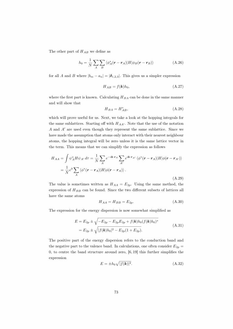
The other part of HAB we define as
h0 =1
N
∑A
∑B
〈φ∗A(r − rA)|H|φB(r − rB)〉 (A.26)
for all A and B where |bm − an| = |δ1,2,3|. This gives us a simpler expression
HAB = f(k)h0, (A.27)
where the first part is known. Calculating HBA can be done in the same mannerand will show that
HBA = H∗AB , (A.28)
which will prove useful for us. Next, we take a look at the hopping integrals forthe same sublattices. Starting off with HAA′ . Note that the use of the notationA and A′ are used even though they represent the same sublattice. Since wehave made the assumption that atoms only interact with their nearest neighbouratoms, the hopping integral will be zero unless it is the same lattice vector inthe term. This means that we can simplify the expression as follows
HAA =
∫ψ∗AHψA′ dτ =
1
N
∑A
e−ik·rA∑A′
eik·rA′ 〈φ∗(r − rA)|H|φ(r − rA′)〉
=1
Ne0∑A
〈φ∗(r − rA)|H|φ(r − rA)〉 .
(A.29)The value is sometimes written as HAA = E2p. Using the same method, theexpression of HBB can be found. Since the two different subsets of lattices allhave the same atoms
HAA = HBB = E2p. (A.30)
The expression for the energy dispersion is now somewhat simplified as
E = E2p ±√−E2p − E2pE2p + f(k)h0(f(k)h0)∗
= E2p ±√|f(k)h0|2 − E2p(1 + E2p).
(A.31)
The positive part of the energy dispersion refers to the conduction band andthe negative part to the valence band. In calculations, one often consider E2p =
0, to centre the band structure around zero, [6, 19] this further simplifies theexpression
E = ±h0
√|f(k)|2. (A.32)
73

We already know the value of |f(k)|2, which can be simplified as
|f(k)|2 = f∗(k)f(k)
=
(e−ikxaC−C + e
iaC−C(
12kx+
√3
2 ky)
+ eiaC−C
(12kx−
√3
2 ky))
·(eikxaC−C + e
−iaC−C(
12kx+
√3
2 ky)
+ e−iaC−C
(12kx−
√3
2 ky))
= 3 + 4 cos
(√3
2kyaC−C
)cos
(3
2kxaC−C
)+ 2 cos
(√3kyaC−C
).
(A.33)Using the same method and technique, while instead approximating so that
the orbitals interact also with their next-nearest neighbours. The energy dis-persion for this approximation can be written as
E±(k) = ± h0
√|f(k)|2 − h1|f(k)|2, (A.34)
where h0 is the hopping integral as described earlier and h1 is the next-nearestneighbour hopping energy defined as
h1 =1
N
∑A
∑B
〈φ∗A(r − rA)|H|φB(r − rB)〉 (A.35)
for all A and B where |bm − an| = |δ1′,2′,3′,4′,5′,6′ | [19, 58].
74

Appendix B
Weyl Hamiltonian forgraphene
Equation 2.9 describes the dispersion relation in graphene near the K-points,the equation is shown figure 2.9 as L and R. Even though (2.9) is often referredto as being linear, |k| does not necessarily have to be linear. For example, ifk = (kx, ky), the energy dispersion is
Eψ = ±~vF√kx2 + ky2 (B.1)
which is not linear. But with some small tricks the useful Weyl Hamiltonian forgraphene can be derived. Firstly, using the deBroglie relationship
p = ~k, (B.2)
the expression for E can be re-written as
Eψ = ±vF√
(~kx)2 + (~ky)2ψ = ±vF√
(px)2 + (py)2ψ. (B.3)
Next, using the following relationship
p = −i~∇, (B.4)
the expression can be written as
Eψ = ±vF√
(−1)2i2~2∇2ψ = ±~vF√−∇2ψ,
= ±i~vF√∇2ψ.
(B.5)
75

Here we can see that we need to take the square root of the Laplacian operator,which makes the problem less trivial than it first appeared. But with the helpof Pythagoras theorem, the absolute value of k can be written in a differentmanner.
k2 = kx2 + ky
2, (B.6)
together with a re-write version of k as a linear function
|k| = k = σxkx + σyky. (B.7)
From this a relationship between σ and k can be expressed such as
k = σxkx + σyky
⇔
k2 = (σxkx + σyky)2
⇔
kx2 + ky
2 = σ2xkx
2 + (σxσy + σyσx)kxky + σ2yky
2
⇔ σ2x = 1
σ2y = 1
σxσy + σyσx = 0.
(B.8)
A re-write of (B.5), using equations (B.2) and (B.4) as well and the notationσ = (σx, σy) gives [29]
Eψ = ±i~vFσ · k = ±ivFσ · p = ±vFσ · (−i~∇) (B.9)
Which is how we get the Hamiltonian for massless Dirac particles, the so calledWeyl Hamiltonian [59]
H = −i~vFσ ·∇, (B.10)
commonly used in research literature [29].
Eψ = ±i~vF(σx
δ
δx+ σy
δ
δy
)ψ. (B.11)
76

Bibliography
[1] F. Schwierz, “Graphene transistors: status, prospects, and problems,”Proc. IEEE, vol. 101, no. 7, pp. 1567–1584, May 2013. [Online]. Available:http://ieeexplore.ieee.org/document/6518205/ [Accessed: 03-Oct-2016].
[2] C. Pugnaghi et al., “Semianalytical quantum model for graphene field-effect transistors,” J. Appl. Phys., vol. 116, no. 114505, pp. 1–9, 2014.[Online]. Available: http://scitation.aip.org/content/aip/journal/jap/116/11/10.1063/1.4895993 [Accessed: 04-Oct-2016].
[3] A. C. Ferrari et al., “Science and technology roadmap for graphene,related two-dimensional crystals, and hybrid systems,” Nanoscale,vol. 7, no. 11, pp. 4598–4810, 2015. [Online]. Available: http://dx.doi.org/10.1039/C4NR01600A [Accessed: 11-Oct-2016].
[4] S. Rakheja et al., “A unified charge-current compact model for ambipolaroperation in quasi-ballistic graphene transistors: Experimental verificationand circuit-analysis demonstration,” in 2013 IEEE International ElectronDevices Meeting. Washington, DC, USA: IEEE, Dec. 2013, pp. 5.5.1–5.5.4. [Online]. Available: http://ieeexplore.ieee.org/document/6724568/[Accessed: 15-Nov-2016].
[5] J. Handy, “How many transistors have ever shipped?” Forbes, 2014.[Online]. Available: https://www.forbes.com/sites/jimhandy/2014/05/26/how-many-transistors-have-ever-shipped/#2a03e9c04425 [Accessed: 29-Oct-2016].
[6] A. H. Castro Neto, F. Guinea, N. M. R. Peres, K. S. Novoselov,and A. K. Geim, “The electronic properties of graphene,” Rev.Mod. Phys., vol. 81, no. 1, p. 109, 2009. [Online]. Available:http://link.aps.org/doi/10.1103/RevModPhys.81.109 [Accessed: 7-Oct-2016].
77
[7] W. Liu, Fundamentals of III-V Devices: HBTs, MESFETs, andHFETs/HEMTs. New York: John Wiley & Sons Inc., 1999.
[8] M. I. Katsnelson, K. S. Novoselov, and A. K. Geim, “Chiral tunnelling andthe klein paradox in graphene,” Nature Phys., vol. 2, no. 9, pp. 620–625,2006. [Online]. Available: http://www.nature.com/nphys/journal/v2/n9/suppinfo/nphys384_S1.html [Accessed: 31-Oct-2016].
[9] D. Dragoman and M. Dragoman, “Negative differential resistance ofelectrons in graphene barrier,” Appl. Phys. Lett., vol. 90, no. 14,pp. 143 111–1–143 111–3, 2007. [Online]. Available: http://scitation.aip.org/content/aip/journal/apl/90/14/10.1063/1.2719670 [Accessed: 27-Oct-2016].
[10] M. I. Katsnelson, “Graphene: carbon in two dimensions,” Mater.Today, vol. 10, no. 1–2, pp. 20–27, 2007. [Online]. Available: http://www.sciencedirect.com/science/article/pii/S1369702106717886 [Accessed:31-Oct-2016].
[11] G. E. Moore, “Cramming more components onto integrated circuits,” Elec-tronics, vol. 38, no. 8, Apr. 1965.
[12] G. E. Moore, “No exponential is forever: but “forever" can be delayed!” inSolid-State Circuits Conference, 2003. Digest of Technical Papers. ISSCC.2003 IEEE International. IEEE, 2003, pp. 20–23. [Online]. Available:http://ieeexplore.ieee.org/document/1234194 [Accessed: 03-Oct-2016].
[13] M. C. Lemme, T. J. Echtermeyer, M. Baus, and H. Kurz, “A graphene field-effect device,” IEEE Electron Device Lett., vol. 28, no. 4, pp. 282–284, apr2007. [Online]. Available: http://ieeexplore.ieee.org/document/4137639/[Accessed: 09-Jan-2017].
[14] J. Tian, A. Katsounaros, D. Smith, and Y. Hao, “Graphene field-effecttransistor model with improved carrier mobility analysis,” IEEE Trans.Electron Devices, vol. 62, no. 10, pp. 3433–3440, 2015. [Online]. Available:http://ieeexplore.ieee.org/document/7230253/ [Accessed: 03-Oct-2016].
[15] G. M. Landauer, D. Jimenez, and J. L. González, “An accurate and verilog-a compatible compact model for graphene field-effect transistors,” IEEETrans. Nanotechnol., vol. 13, no. 5, pp. 895–904, 2014. [Online]. Available:http://ieeexplore.ieee.org/document/6825842/ [Accessed: 25-Oct-2016].
[16] D. Jimenez and O. Moldovan, “Explicit drain-current model of graphenefield-effect transistors targeting analog and radio-frequency applications,”
78

IEEE Trans. Electron Devices, vol. 58, no. 11, pp. 4049–4052,2011. [Online]. Available: http://ieeexplore.ieee.org/abstract/document/6018290/ [Accessed: 25-Oct-2016].
[17] “Advanced design system (ads) 2016.01,” Keysight Technologies, SantaRosa, CA, United States, 2016. [Online]. Available: http://www.keysight.com/en/pc-1297113/advanced-design-system
[18] “Matlab version 9.0.0.341360 (r2016a),” The Mathworks, Inc., Natick,Massachusetts, United States, 2016. [Online]. Available: http://www.mathworks.com/products/matlab/
[19] M. Andersson, “Characterisation and modelling of graphene FETs for ter-ahertz mixers and detectors,” Ph.D. dissertation, Chalmers University ofTechnology, Gothenburg, 2016.
[20] D. Reddy, L. F. Register, G. D. Carpenter, and S. K. Banerjee, “Graphenefield-effect transistors,” J. Phys. D: Appl. Phys., vol. 44, no. 31, pp.1–20, 2011. [Online]. Available: http://stacks.iop.org/0022-3727/44/i=31/a=313001 [Accessed: 26-Oct-2016].
[21] P. R. Wallace, “The band theory of graphite,” Phys. Rev., vol. 71, pp.622–634, May 1947. [Online]. Available: http://link.aps.org/doi/10.1103/PhysRev.71.622 [Accessed: 3-Feb-2017].
[22] R. J. Tilley, Crystals and crystal structures. John Wiley & Sons, 2006.
[23] W. Setyawan and S. Curtarolo, “High-throughput electronic band structurecalculations: Challenges and tools,” Comput. Mater. Sci., vol. 49, no. 2,pp. 299 – 312, 2010. [Online]. Available: http://www.sciencedirect.com/science/article/pii/S0927025610002697 [Accessed: 5-Dec-2016].
[24] V. Nam Do, V. Nguyen Hung, P. Dollfus, and A. Bournel, “Electronictransport and spin-polarization effects of relativisticlike particles inmesoscopic graphene structures,” J. Appl. Phys., vol. 104, no. 6,pp. 063 708–1–063 708–7, 2008. [Online]. Available: http://scitation.aip.org/content/aip/journal/jap/104/6/10.1063/1.2980045 [Accessed: 28-Oct-2016].
[25] A. Mangla, “Modeling nanoscale quasi-ballistic MOS transistors: a circuitdesign perspective,” Ph.D. dissertation, École Polytechnique Fédérale deLausanne, Lausanne, 2014. [Online]. Available: https://infoscience.epfl.ch/record/203255/files/EPFL_TH6385.pdf [Accessed: 14-Oct-2016].
79

[26] M. O. Goerbig, “Electronic properties of graphene in a strong magneticfield,” Rev. Mod. Phys., vol. 83, no. 4, p. 1193, 2011. [Online].Available: http://journals.aps.org/rmp/abstract/10.1103/RevModPhys.83.1193 [Accessed: 23-Feb-2017].
[27] C. González, J. Ruiz, R. Bonilla, and A. Ávila, “Quan-tum tunnelling demonstration using a low-cost experimental setup,”in Micro-Nanoelectronics, Technology and Applications (EAMTA),2013 7th Argentine School of Micro-Nanoelectronics, Technologyand Applications. IEEE, 2013, pp. 78–85. [Online]. Available:http://ieeexplore.ieee.org/abstract/document/6621082/ [Accessed: 2-Mar-2017].
[28] O. Klein, “Die reflexion von elektronen an einem potentialsprungnach der relativistischen dynamik von dirac,” Zeitschrift für Physik,vol. 53, no. 3, pp. 157–165, 1929. [Online]. Available: https://link.springer.com/article/10.1007%2FBF01339716 [Accessed: 9-Mar-2017].
[29] T. Robinson, “On klein tunneling in graphene,” Am. J. Phys., vol. 80, no. 2,pp. 141–147, 2012.
[30] N. Dombey and A. Calogeracos, “Seventy years of the klein paradox,”Phys. Rep., vol. 315, no. 1, pp. 41–58, 1999. [Online]. Available: http://www.sciencedirect.com/science/article/pii/S037015739900023X [Accessed:9-Mar-2017].
[31] H. Hai, F. Xing-Qiu, and H. Rong-Sheng, “Klein paradox of two-dimensional dirac electrons in circular well potential,” Commun.Theor. Phys., vol. 58, no. 2, p. 205–208, 2010. [Online]. Available:http://stacks.iop.org/0253-6102/58/i=2/a=06 [Accessed: 9-Mar-2017].
[32] H. Wang, A. Hsu, J. Kong, D. A. Antoniadis, and T. Palacios,“Compact virtual-source current-voltage model for top-and back-gatedgraphene field-effect transistors,” IEEE Trans. Electron Devices, vol. 58,no. 5, pp. 1523–1533, 2011. [Online]. Available: http://ieeexplore.ieee.org/document/5735198/ [Accessed: 31-Oct-2016].
[33] Y.-S. Woo, S.-A. Seo, D.-C. Kim, and H.-J. Chung, “Electronic device usinga two-dimensional sheet material, transparent display and methods offabricating the same,” U.S. Patent 8 513 653, aug, 2013. [Online]. Available:https://www.google.co.uk/patents/US8513653 [Accessed: 13-Oct-2016].
80

[34] C. News, “Columbia engineers prove graphene is the strongest material,”Columbia News, 2008. [Online]. Available: http://www.columbia.edu/cu/news/08/07/graphene.html [Accessed: 09-Mar-2017].
[35] S. Mirsky, “Elephant illustrates important point,” Sci. Am., 2011. [Online].Available: https://www.scientificamerican.com/article/balancing-act/[Accessed: 10-Mar-2017].
[36] E. H. Hwang and S. Das Sarma, “Acoustic phonon scatteringlimited carrier mobility in two-dimensional extrinsic graphene,” Phys.Rev. B, vol. 77, p. 115449, Mar 2008. [Online]. Available: https://link.aps.org/doi/10.1103/PhysRevB.77.115449 [Accessed: 31-Oct-2016].
[37] K. Bolotin et al., “Ultrahigh electron mobility in suspended graphene,”Solid State Commun., vol. 146, no. 9–10, pp. 351 – 355, 2008.[Online]. Available: http://www.sciencedirect.com/science/article/pii/S0038109808001178 [Accessed: 31-Oct-2016].
[38] P. Sharma, L. S. Bernard, A. Bazigos, A. Magrez, and A. M. Ionescu,“Room-temperature negative differential resistance in graphene field effecttransistors: Experiments and theory,” ACS Nano, vol. 9, no. 1, pp.620–625, 2015. [Online]. Available: http://dx.doi.org/10.1021/nn5059437[Accessed: 28-Oct-2016].
[39] H. Bennett et al., “International technology roadmap for semiconductors2.0 - 2015 edition - beyond CMOS,” 2015. [Online]. Available:http://www.semiconductors.org/clientuploads/Research_Technology/ITRS/2015/6_2015%20ITRS%202.0%20Beyond%20CMOS.pdf [Accessed:1-Jan-2017].
[40] A. K. Geim and K. S. Novoselov, “The rise of graphene,” Nat. Mater.,vol. 6, no. 3, pp. 183–191, 2007. [Online]. Available: http://www.nature.com/nmat/journal/v6/n3/abs/nmat1849.html [Accessed: 7-Jan-2017].
[41] W. Shockley, “A unipolar “field-effect” transistor,” Proc. IRE, vol. 40,no. 11, pp. 1365–1376, nov 1952. [Online]. Available: http://ieeexplore.ieee.org/document/4050836/ [Accessed: 29-Oct-2016].
[42] S.-L. Li, H. Miyazaki, A. Kumatani, A. Kanda, and K. Tsukagoshi,“Low operating bias and matched input- output characteristics ingraphene logic inverters,” Nano Lett., vol. 10, no. 7, pp. 2357–2362,2010. [Online]. Available: http://pubs.acs.org/doi/abs/10.1021/nl100031x[Accessed: 24-Mar-20170].
81

[43] R. Cheng et al., “High-frequency self-aligned graphene transistorswith transferred gate stacks,” Proc. Natl. Acad. Sci. U.S.A., vol.109, no. 29, pp. 11 588–11 592, 2012. [Online]. Available: http://www.pnas.org/content/109/29/11588 [Accessed: 11-Jan-2017].
[44] F. Schwierz, “Graphene transistors,” Nat. Nanotech., vol. 5, no. 7,pp. 487–496, 2010. [Online]. Available: http://www.nature.com/nnano/journal/v5/n7/full/nnano.2010.89.html [Accessed: 3-Nov-2016].
[45] S. A. Thiele, J. A. Schaefer, and F. Schwierz, “Modeling of graphenemetal-oxide-semiconductor field-effect transistors with gapless large-areagraphene channels,” J. Appl. Phys., vol. 107, no. 9, pp. 094 505–1–094 505–8,2010. [Online]. Available: http://aip.scitation.org/doi/10.1063/1.3357398[Accessed: 17-Jan-2017].
[46] R. Yan et al., “Determination of graphene work function and graphene-insulator-semiconductor band alignment by internal photoemissionspectroscopy,” Appl. Phys. Lett., vol. 101, no. 2, pp. 022 105–1–022 105–4,2012. [Online]. Available: http://aip.scitation.org/doi/10.1063/1.4734955[Accessed: 11-Jan-2017].
[47] D. Jimenez, “Explicit drain current, charge and capacitance modelof graphene field-effect transistors,” IEEE Trans. Electron Devices,vol. 58, no. 12, pp. 4377–4383, dec 2011. [Online]. Available:http://ieeexplore.ieee.org/document/6054021/ [Accessed: 21-Nov-2016].
[48] S. Rakheja et al., “An ambipolar virtual-source-based charge-currentcompact model for nanoscale graphene transistors,” IEEE Trans.Nanotechnol., vol. 13, no. 5, pp. 1005–1013, 2014. [Online]. Available:http://ieeexplore.ieee.org/document/6868269/ [Accessed: 15-Nov-2016].
[49] T. Fang, A. Konar, H. Xing, and D. Jena, “Carrier statisticsand quantum capacitance of graphene sheets and ribbons,” Appl.Phys. Lett., vol. 91, no. 9, pp. 092 109–1–092 109–3, aug 2007.[Online]. Available: http://scitation.aip.org/content/aip/journal/apl/91/9/10.1063/1.2776887 [Accessed: 7-Nov-2016].
[50] Y. Wu et al., “Three-terminal graphene negative differential resistancedevices,” ACS Nano, vol. 6, no. 3, pp. 2610–2616, 2012. [Online]. Available:http://dx.doi.org/10.1021/nn205106z [Accessed: 27-Oct-2016].
[51] K. N. Parrish, M. E. Ramón, S. K. Banerjee, and D. Akinwande, “A com-pact model for graphene fets for linear and non-linear circuits,” in IEEE
82
17th International Conference on Simulation of Semiconductor Processesand Devices, Denver, CO, USA, 2012, pp. 75–78.
[52] A. Mangla, J.-M. Sallese, C. Sampedro, F. Gamiz, and C. Enz, “Role ofthe gate in ballistic nanowire SOI MOSFETs,” Solid-State Electron., vol.112, pp. 24–28, 2015. [Online]. Available: http://www.sciencedirect.com/science/article/pii/S0038110115000556 [Accessed: 24-Oct-2016].
[53] A. Mangla, J.-M. Sallese, C. Sampedro, F. Gamiz, and C. Enz, “Modelingthe channel charge and potential in quasi-ballistic nanoscale double-gateMOSFETs,” IEEE Trans. Electron Devices, vol. 61, no. 8, pp. 2640–2646,2014. [Online]. Available: http://ieeexplore.ieee.org/document/6832484/[Accessed: 18-Oct-2016].
[54] E. Gnani, A. Gnudi, S. Reggiani, and G. Baccarani, “Quasi-ballistictransport in nanowire field-effect transistors,” IEEE Trans. ElectronDevices, vol. 55, no. 11, pp. 2918–2930, 2008. [Online]. Available:http://ieeexplore.ieee.org/document/4648223/ [Accessed: 26-Oct-2016].
[55] V. E. Dorgan, M.-H. Bae, and E. Pop, “Mobility and saturation velocityin graphene on sio2,” Appl. Phys. Lett., vol. 97, no. 8, pp. 082 112–1–082 112–3, 2010. [Online]. Available: http://dx.doi.org/10.1063/1.3483130[Accessed: 13-Feb-2017].
[56] I. Meric et al., “Current saturation in zero-bandgap, top-gated graphenefield-effect transistors,” Nat. Nanotech., vol. 3, no. 11, pp. 654–659, 2008.[Online]. Available: http://www.nature.com/nnano/journal/v3/n11/full/nnano.2008.268.html [Accessed: 3-Nov-2016].
[57] S. Thiele and F. Schwierz, “Modeling of the steady state characteristics oflarge-area graphene field-effect transistors,” J. Appl. Phys., vol. 110, no. 3,p. 034506, 2011. [Online]. Available: http://aip.scitation.org/doi/10.1063/1.3606583 [Accessed: 3-Nov-2016].
[58] P. A. M. Dirac, The principles of quantum mechanics, 3rd ed. ClarendonPress, 1974.
[59] L. Lu et al., “Experimental observation of weyl points,” Science,vol. 349, no. 6248, pp. 622–624, 2015. [Online]. Available: http://science.sciencemag.org/content/349/6248/622 [Accessed: 9-Mar-2017].
83

Modelling GrapheneField-Effect Transistors
SOFIA SJÖLANDERMASTER´S THESISDEPARTMENT OF ELECTRICAL AND INFORMATION TECHNOLOGYFACULTY OF ENGINEERING | LTH | LUND UNIVERSITY
Printed by Tryckeriet i E-huset, Lund 2018
SOFIA
SJÖLA
ND
ERM
odelling Graphene Field-Effect Transistors
LUN
D 2018
Series of Master’s thesesDepartment of Electrical and Information Technology
LU/LTH-EIT 2018-617
http://www.eit.lth.se