
Mobility and homogeneity efiects on the power conversion e ...
211
Mobility and homogeneity effects on the power conversion efficiency of solar cells Von der Fakult¨ at Informatik, Elektrotechnik und Informationstechnik der Universit¨ at Stuttgart zur Erlangung der W¨ urde eines Doktor-Ingenieurs (Dr.-Ing.) genehmigte Abhandlung Vorgelegt von Julian Mattheis geboren am 14.12.1975 in Hannover Hauptberichter: Prof. Dr. rer. nat. habil. J. H. Werner Mitberichter: Prof. Dr. rer. nat. habil. U. Rau Prof. Dr. E. Kasper Tag der Einreichung: 20.06.2007 Tag der m¨ undlichen Pr¨ ufung: 08.01.2008 Institut f¨ ur Physikalische Elektronik der Universit¨ at Stuttgart 2008
Transcript of Mobility and homogeneity efiects on the power conversion e ...

Mobility and homogeneity effectson the power conversion efficiency
of solar cells
Von der Fakultat Informatik, Elektrotechnik und Informationstechnik
der Universitat Stuttgart zur Erlangung der Wurde eines
Doktor-Ingenieurs (Dr.-Ing.) genehmigte Abhandlung
Vorgelegt von
Julian Mattheis
geboren am 14.12.1975 in Hannover
Hauptberichter: Prof. Dr. rer. nat. habil. J. H. Werner
Mitberichter: Prof. Dr. rer. nat. habil. U. Rau
Prof. Dr. E. Kasper
Tag der Einreichung: 20.06.2007
Tag der mundlichen Prufung: 08.01.2008
Institut fur Physikalische Elektronik der Universitat Stuttgart
2008


Contents
Abstract v
Zusammenfassung vii
1 Introduction 1
1.1 Structure . . . . . . . . . . . . . . . . . . . . . . . . . . . . . . . . . . 2
2 Efficiency limits of solar cells 4
2.1 Classification of solar cell models . . . . . . . . . . . . . . . . . . . . . 5
2.1.1 Classification scheme . . . . . . . . . . . . . . . . . . . . . . . . 7
2.2 Current-voltage characteristic of solar cells . . . . . . . . . . . . . . . . 9
2.3 Radiative efficiency limit . . . . . . . . . . . . . . . . . . . . . . . . . . 9
2.3.1 Complete carrier collection . . . . . . . . . . . . . . . . . . . . . 10
2.3.2 Incomplete carrier collection . . . . . . . . . . . . . . . . . . . . 14
2.4 Classical diode theory . . . . . . . . . . . . . . . . . . . . . . . . . . . 15
2.4.1 Incomplete carrier collection . . . . . . . . . . . . . . . . . . . . 15
2.4.2 Complete carrier collection . . . . . . . . . . . . . . . . . . . . . 16
3 Generalized efficiency limit 18
3.1 Radiative recombination and photon recycling . . . . . . . . . . . . . . 19
3.2 Photon recycling in the literature . . . . . . . . . . . . . . . . . . . . . 20
3.3 Diffusion equation with reabsorption . . . . . . . . . . . . . . . . . . . 22
3.3.1 Parameter normalization . . . . . . . . . . . . . . . . . . . . . . 24
3.3.2 Free parameters . . . . . . . . . . . . . . . . . . . . . . . . . . . 26
3.4 Results with constant absorption coefficient . . . . . . . . . . . . . . . 27
3.4.1 Radiative efficiency limit . . . . . . . . . . . . . . . . . . . . . . 28
i
ii CONTENTS
3.4.2 Non-radiative recombination . . . . . . . . . . . . . . . . . . . . 32
3.5 Photon recycling and detailed balance . . . . . . . . . . . . . . . . . . 35
3.5.1 Radiation balance in equilibrium . . . . . . . . . . . . . . . . . 35
3.5.2 Non-equilibrium concentration profile . . . . . . . . . . . . . . . 40
3.5.3 Radiation balance in non-equilibrium . . . . . . . . . . . . . . . 42
3.5.4 Reciprocity between solar cell and light emitting diode . . . . . 47
3.6 Critical mobility . . . . . . . . . . . . . . . . . . . . . . . . . . . . . . . 49
3.6.1 High mobility limit - absorptance . . . . . . . . . . . . . . . . . 50
3.6.2 Low mobility limit . . . . . . . . . . . . . . . . . . . . . . . . . 52
3.6.3 Critical mobility in the radiative recombination limit . . . . . . 55
3.6.4 Critical mobility for non-radiative recombination . . . . . . . . 57
3.7 Analytical approximation . . . . . . . . . . . . . . . . . . . . . . . . . . 57
3.7.1 Analytical approximations in the literature . . . . . . . . . . . . 59
3.7.2 Two-layer model . . . . . . . . . . . . . . . . . . . . . . . . . . 61
3.7.3 Modified-lifetime model . . . . . . . . . . . . . . . . . . . . . . 61
3.7.4 Evaluation of the approximation . . . . . . . . . . . . . . . . . . 64
3.8 Energy-dependent absorption coefficient . . . . . . . . . . . . . . . . . 71
3.8.1 Thickness-dependent current enhancement . . . . . . . . . . . . 75
3.8.2 Thickness-dependent efficiency enhancement . . . . . . . . . . . 77
3.8.3 Maximum open circuit voltage . . . . . . . . . . . . . . . . . . . 79
3.9 Maximum efficiencies of real materials . . . . . . . . . . . . . . . . . . 80
3.9.1 Analytical approximation . . . . . . . . . . . . . . . . . . . . . 82
3.9.2 Critical mobility . . . . . . . . . . . . . . . . . . . . . . . . . . 89
3.9.3 Discussion . . . . . . . . . . . . . . . . . . . . . . . . . . . . . . 91
3.10 Limitations to the model . . . . . . . . . . . . . . . . . . . . . . . . . . 95
3.11 Conclusion . . . . . . . . . . . . . . . . . . . . . . . . . . . . . . . . . . 96
4 Band gap fluctuations 98
4.1 Disorder and band gap fluctuations . . . . . . . . . . . . . . . . . . . . 101
4.2 Band gap fluctuations model . . . . . . . . . . . . . . . . . . . . . . . . 101
4.2.1 Light absorption . . . . . . . . . . . . . . . . . . . . . . . . . . 103
4.2.2 Light emission . . . . . . . . . . . . . . . . . . . . . . . . . . . . 104
4.2.3 Discussion . . . . . . . . . . . . . . . . . . . . . . . . . . . . . . 113

CONTENTS iii
4.3 Numerical approach . . . . . . . . . . . . . . . . . . . . . . . . . . . . . 115
4.3.1 Formulation of the problem . . . . . . . . . . . . . . . . . . . . 116
4.3.2 Correlated band gap sequence . . . . . . . . . . . . . . . . . . . 118
4.3.3 Discussion . . . . . . . . . . . . . . . . . . . . . . . . . . . . . . 119
4.4 Experimental results . . . . . . . . . . . . . . . . . . . . . . . . . . . . 121
4.5 Discussion . . . . . . . . . . . . . . . . . . . . . . . . . . . . . . . . . . 124
4.5.1 Length-scale of band gap fluctuations . . . . . . . . . . . . . . . 124
4.5.2 Origin of band gap fluctuations . . . . . . . . . . . . . . . . . . 128
4.5.3 Model refinements . . . . . . . . . . . . . . . . . . . . . . . . . 130
4.5.4 Implications for solar cell performance . . . . . . . . . . . . . . 133
4.6 Conclusions . . . . . . . . . . . . . . . . . . . . . . . . . . . . . . . . . 134
5 Outlook 136
A Radiative efficiency limit with energy-dependent absorptance 138
A.1 Inhomogeneous band gap . . . . . . . . . . . . . . . . . . . . . . . . . . 138
A.2 Optimal absorptance . . . . . . . . . . . . . . . . . . . . . . . . . . . . 140
B Derivation and numerical implementation of the photon recycling
scheme 144
B.1 Exponential Integrals . . . . . . . . . . . . . . . . . . . . . . . . . . . . 144
B.2 Diffusion equation with reabsorption . . . . . . . . . . . . . . . . . . . 146
B.2.1 Linear matrix formalism . . . . . . . . . . . . . . . . . . . . . . 146
B.2.2 Transport . . . . . . . . . . . . . . . . . . . . . . . . . . . . . . 149
B.2.3 Recombination . . . . . . . . . . . . . . . . . . . . . . . . . . . 149
B.2.4 Direct internal generation . . . . . . . . . . . . . . . . . . . . . 150
B.2.5 Internal generation after multiple reflections . . . . . . . . . . . 153
B.2.6 External generation . . . . . . . . . . . . . . . . . . . . . . . . . 160
B.3 Generation terms . . . . . . . . . . . . . . . . . . . . . . . . . . . . . . 162
B.3.1 Internal generation . . . . . . . . . . . . . . . . . . . . . . . . . 163
B.3.2 External generation . . . . . . . . . . . . . . . . . . . . . . . . . 166
B.4 Diffusion operator . . . . . . . . . . . . . . . . . . . . . . . . . . . . . . 168
B.5 Boundary conditions . . . . . . . . . . . . . . . . . . . . . . . . . . . . 169
B.5.1 Back contact . . . . . . . . . . . . . . . . . . . . . . . . . . . . 169

iv CONTENTS
B.5.2 Junction . . . . . . . . . . . . . . . . . . . . . . . . . . . . . . . 170
B.6 Discussion . . . . . . . . . . . . . . . . . . . . . . . . . . . . . . . . . . 170
B.6.1 Reabsorption matrix . . . . . . . . . . . . . . . . . . . . . . . . 170
B.6.2 Energy superposition . . . . . . . . . . . . . . . . . . . . . . . . 171
B.7 Numerical error sources . . . . . . . . . . . . . . . . . . . . . . . . . . . 171
B.7.1 Optical limitations - absorption length . . . . . . . . . . . . . . 171
B.7.2 Electrical limitations - diffusion length . . . . . . . . . . . . . . 173
C Derivation of the two-layer model 174
Nomenclature 179
Bibliography 184
Curriculum Vitae 194
List of Publications 195
Danksagung 197

Abstract
The thesis on hand investigates the interplay between detailed radiation balances and
charge carrier transport. The first part analyzes the role of limited carrier transport for
the efficiency limits of pn-junction solar cells. The second part points out the influence
of transport on the absorption and emission of light in inhomogeneous semiconductors.
By incorporating an integral term that accounts for the repeated internal emission
and reabsorption of photons (the so-called photon recycling) into the diffusion equation
for the minority carriers, the first part of the thesis develops a self-consistent model
that is capable of describing the power conversion efficiencies of existing devices as well
as of devices in the radiative recombination limit. The model thus closes the gap be-
tween the classical diode theory and the Shockley Queisser detailed balance efficiency
limit. While the model converges towards the Shockley Queisser limit when recombi-
nation is exclusively radiative and the minority carrier mobility is infinity, it converges
towards the classical diode theory once the minority carrier lifetime is dominated by
non-radiative recombination. It is shown that the classical diode theory without the
inclusion of photon recycling produces accurate results only if the minority carrier life-
time is at least ten times smaller than the radiative lifetime. The thesis shows that even
in the radiative recombination limit, charge carrier transport is extremely important.
The efficiency is reduced drastically once the minority carrier mobility drops below a
critical mobility even under otherwise most ideal conditions. A closed-form expression
is derived for this critical mobility, which depends on the absorption coefficient and
the doping concentration. The thesis thus presents a universal criterion that needs
to be fulfilled by any photovoltaic material in order to obtain high power conversion
efficiency. The numerical results are analyzed and compared to an analytical approx-
imation. This approximation is capable of describing the efficiency of solar cells with
assumed energy-independent absorption coefficient. While it also accurately predicts
v

vi ABSTRACT
the open circuit voltage of solar cells with energy-dependent absorption coefficient, it
is only a rough estimate for the short circuit current. The thesis applies the developed
model to solar cells made of crystalline silicon, amorphous silicon and Cu(In,Ga)Se2
(CIGS). It shows that crystalline silicon solar cells neither have transport problems in
the radiative recombination limit nor in existing devices. In Cu(In,Ga)Se2 solar cells,
mobilities are at most two orders of magnitude above the critical mobility and guaran-
tee complete carrier collection only close to the radiative limit. Existing devices utilize
graded band gaps equally as a means of passivating the back contact and for increasing
carrier collection in the bulk. Amorphous silicon solar cells, however, not only need to
overcome insufficient carrier collection in existing devices by means of built-in electric
fields, but also come close to being limited by carrier collection even in the radiative
limit.
The second part of the thesis investigates the role of carrier transport for the absorp-
tion and emission of light in semiconductors with band gap fluctuations. The chapter
develops an analytical statistical model to describe the absorption and emission spec-
tra of such inhomogeneous semiconductors. Particular emphasis is placed on the role
of the length-scale of the band gap fluctuations. As it turns out, the crucial quan-
tity with respect to the emission spectrum is the ratio of the charge carrier transport
length and the length-scale of the band gap fluctuations. Both, absorption edge and
emission peak are broadened by band gap fluctuations. While the absorption spec-
trum is not influenced by the length scale of the fluctuations, the developed model
shows that the spectral position of the emission peak relative to the absorption edge
depends on the ratio of fluctuation length and transport length. Comparison with
numerical simulations underlines the importance of the fluctuation length in relation
to the diffusion length and also points out the influence of the magnitude of the band
gap fluctuations in terms of the standard deviation of the fluctuations. The model is
applied to experimental absorption and photoluminescence data of Cu(In,Ga)Se2 thin
films with varying gallium content. The ternary compounds CuInSe2 and CuGaSe2
exhibit the smallest magnitude of fluctuations with standard deviations in the range
of 20− 40 meV. The fact that the quaternary compounds show standard deviations of
up to 65 meV points to alloy disorder as one possible source of band gap fluctuations.
All observed fluctuations occur on a very small length scale that is at least ten times
smaller than the electron diffusion length of approximately 1 µm.

Zusammenfassung
Die vorliegende Arbeit untersucht das Zusammenspiel von detailierten Strahlungs-
gleichgewichten mit dem Transport von Ladungstragern. Der erste Teil analysiert
die Bedeutung von begrenztem Ladungstragertransport fur die Wirkungsgradgrenzen
von pn-Ubergang Solarzellen. Der zweite Teil zeigt den Einfluss von Transport auf die
Absorption und Emission von Licht in inhomogenen Halbleitern auf.
Zur Berucksichtigung der wiederholten internen Emission und Reabsorption von
Photonen (des sog. Photon Recyclings) baut der erste Teil der Arbeit einen Inte-
gralterm in die Diffusionsgleichung fur die Minoritatsladungstrager ein. Dadurch wird
wird ein selbstkonsistentes Modell entwickelt, das in der Lage ist, den Wirkungsgrad
von realen Solarzellen ebenso zu beschreiben wie den idealen Wirkungsgrad im Limit
strahlender Rekombination. Das Modell schließt somit die Lucke zwischen der klassi-
schen Diodentheorie und dem aus der detailierten Bilanz abgeleiteten Shockley Queisser
Wirkungsgrad Limit. Wahrend das Modell gegen das Shockley Queisser Limit kon-
vergiert, wenn Rekombination ausschließlich strahlend und die Minoritatstrager Be-
weglichkeit unendlich ist, geht es in die klassische Diodentheorie uber, wenn die Mi-
noritatstragerlebensdauer durch nicht-strahlende Rekombination dominiert wird. Es
wird gezeigt, dass die klassische Diodentheorie ohne die Berucksichtigung von Photon
Recycling nur hinreichend genaue Resultate produziert, wenn die Minoritatstragerle-
bensdauer mindestens zehnmal kleiner ist als die strahlende Lebensdauer. Die Ar-
beit zeigt, dass Ladungstragertransport sogar im strahlenden Wirkungsgrad Limit
von hochster Wichtigkeit ist. Selbst unter ansonsten idealen Bedingungen wird der
Wirkungsgrad drastisch reduziert, sobald die Minoritatstragerbeweglichkeit kleiner als
eine kritische Beweglichkeit ist. Es wird ein einfacher analytischer Ausdruck fur die kri-
tische Beweglichkeit hergeleitet, die vom Absorptionskoeffizienten und der Dotierung
abhangt. Damit prasentiert diese Arbeit ein universales Kriterium, das von jedem
vii

viii ZUSAMMENFASSUNG
photovoltaischen Material erfullt werden muss, um einen hohen Wirkungsgrad zu er-
reichen. Die numerischen Resultate werden analysiert und mit einem analytischen
Modell verglichen. Dieses analytische Modell ist in der Lage, den Wirkungsgrad von
Solarzellen mit energieunabhangigem Absorptionskoeffizienten zu beschreiben. Wah-
rend es ebenso die Leerlaufspannung von Solarzellen mit energieabhangigem Absorp-
tionskoeffizienten korrekt approximiert, erbringt das analytische Modell in diesem Fall
jedoch nur eine ungefahre Naherung fur den Kurzschlussstrom. Die Arbeit wendet das
entwickelte Modell auf Solarzellen aus kristallinem und amorphem Silizium und aus
Cu(In,Ga)Se2 an. Es zeigt sich, dass Solarzellen aus kristallinem Silizium weder im
strahlenden Limit noch in existierenden Solarzellen durch eine zu kleine Beweglichkeit
begrenzt sind. In Solarzellen aus Cu(In,Ga)Se2 sind die Mobilitaten nur maximal zwei
Großenordnungen großer als die kritische Beweglichkeit und garantieren vollstandige
Ladungstragersammlung daher nur sehr dicht am strahlenden Limit. Real existierende
Zellen nutzen gradierte Bandlucken zur Sammlungsunterstutzung im Volumen ebenso
wie zur Ruckseitenpassivierung. Solarzellen aus amorphem Silizium hingegen mussen
nicht nur in realen Bauelementen eingebaute elektrische Felder zur Sammlungsun-
terstutzung einsetzen. Auch im Grenzfall rein strahlender Rekombination sind die
Mobilitaten in der Nahe der kritischen Mobilitat und somit unter Umstanden nicht
ausreichend, um eine vollstandige Ladungstragersammlung zu gewahrleisten.
Der zweite Teil der Arbeit untersucht die Bedeutung von Ladungstragertransport
fur die Absorption und Emission von Licht in Halbleitern mit Bandluckenfluktuatio-
nen. Dieses Kapitel entwickelt ein analytisches statistisches Modell zur Beschreibung
von Absorptions- und Emissionsspektren solch inhomogener Halbleiter. Besonderes
Augenmerk wird dabei auf die Rolle der Langenskala von Bandluckenfluktuationen
gelegt. Wie sich herausstellt, ist die entscheidende Große in Bezug auf das Emission-
sspektrum das Verhaltnis aus der charakteristischen Ladungstrager Transportlange und
der Fluktuationslange der Bandluckenfluktuationen. Sowohl Absorptionskante als auch
der Emissionspeak werden durch Bandluckenfluktuationen verbreitert. Wahrend das
Absorptionsspektrum jedoch unbeeinflusst von der Langenskala der Fluktuationen ist,
zeigt das entwickelte Modell, dass die spektrale Position des Emissionspeaks relativ
zur Lage der Absorptionskante von dem Verhaltnis aus Transportlange und Fluktu-
ationslange abhangt. Der Vergleich mit numerischen Simulationen unterstreicht die
Bedeutung der Fluktuationslange im Vergleich zur Transportlange. Aufgezeigt wird

ZUSAMMENFASSUNG ix
außerdem der Einfluss der Fluktuationshohe, ausgedruckt durch die Standardabwei-
chung der Fluktuationen. Das Modell wird auf experimentelle Absorptions- und Pho-
tolumineszenzdaten von Cu(In,Ga)Se2 Filmen mit verschiedenem Gallimgehalt ange-
wandt. die ternaren Verbindungen CuInSe2 und CuGaSe2 weisen die geringsten Fluk-
tuationen mit Standardabweichungen zwischen 20 und 40 meV auf. Der Umstand,
dass die quaternaren Systeme Standardabweichungen von bis zu 65 meV besitzen,
deutet darauf hin, dass Unordnung infolge der Legierung eine mogliche Ursache der
Bandluckenfluktuationen darstellen. Alle beobachteten Fluktuationen besitzen eine
sehr kurze Fluktuationslange, die mindestens zehnmal kleiner ist als die Elektronen
Diffusionslange von ca. 1 µm.


Chapter 1
Introduction
Today, the biggest share of the world output of solar cells is made of crystalline sili-
con. This dominance of crystalline silicon is owed to the long history of experience in
silicon microelectronics [1]. From a perspective based on the suitability of silicon as a
photovoltaic absorber material, however, this dominance seems rather astonishing. In
particular, the low absorption coefficient seems to disqualify the indirect semiconductor
silicon as the photovoltaic material of choice.
Therefore, a lot of effort has been put in the investigation of new high-absorption
thin-film materials [2–4], such as amorphous silicon [5], Cu(In,Ga)Se2 [6], organic semi-
conductors [7], or organic dyes [8]. However, so far, these so-called second generation [9]
thin-film solar cells have not yet lived up to expectations. They all fall short of achiev-
ing the efficiencies reached with conventional first-generation silicon solar cells.
Of course, the absorption of light is only the first step to the successful conversion
of optical into electrical energy. The photo-generated charge carriers also need to
be separated before they recombine. Obviously, this requires high carrier lifetimes.
However, one factor which is often overlooked in this context is the importance of charge
carrier transport. High lifetimes guarantee high open circuit voltages. Additional high
mobilities are needed to achieve high short circuit current. While many of the new
materials under consideration, in particular the organic materials, feature excellent
lifetimes and open circuit voltages, most of them suffer from low short circuit currents
caused by insufficient carrier mobilities.
This problem is well known in existing devices. Means to improve carrier collection
include the application of pin structures in amorphous silicon, graded band gaps in
1
2 CHAPTER 1. INTRODUCTION
Cu(In,Ga)Se2, or enlarged junction areas in the case of dye-sensitized solar cells.
However, up to now it remains unclear, what influence carrier transport has on the
efficiency limits of solar cells. Such efficiency limits have only been calculated for de-
vices with assumed complete carrier collection. The efficiency limits of photovoltaic
energy conversion are reached when all heat-dissipating loss-mechanisms are avoided.
In accordance with the principle of detailed balance, the only unavoidable loss mech-
anism is radiative recombination. This is because in thermodynamic equilibrium all
thermal radiation from outside the solar cell needs to be balanced by an equal radiation
flux from within the cell. Hence, a general treatment of solar cell efficiencies needs to
address radiation balances as well as charge carrier transport.
An extra dimension is added to the problem by inhomogeneous material parameters,
such as the fundamental band gap. While the laws governing the radiative interaction
between the solar cell and its ambience, i.e., the reciprocity between light absorption
and emission, are still valid locally on a microscopic scale, they need to be modified on
a macroscopic level. Once again, the description of the macroscopic radiation balances
needs to take into account transport phenomena.
1.1 Structure
This thesis investigates the role of carrier transport and inhomogeneous band gaps for
the radiation balances between absorbed and emitted radiation, which determine the
efficiency limits of pn-junction solar cells. The thesis is structured as follows:
Chapter 2 delineates existing theories to describe the efficiencies of solar cells. It
classifies solar cells according to complete and incomplete collection of photo-generated
carriers and points out the shortcomings of the existing theories when it comes to
describe the efficiencies of solar cells with incomplete carrier collection.
Chapter 3 is the main chapter of this thesis. It develops a generalized numerical
model that combines issues of carrier transport and radiation balances which is capable
of describing solar cell efficiencies for all combinations of radiative or non-radiative re-
combination and complete or incomplete carrier collection. The chapter points out the
importance of carrier transport for the solar cell efficiency even under otherwise most
ideal conditions. It shows that the efficiency is reduced sharply once the mobility drops
below a critical mobility. Subsequently, the chapter develops an analytical approxima-

1.1 STRUCTURE 3
tion of the numerical model. It closes with the efficiency limits of real pn junction solar
cells made from crystalline silicon, amorphous silicon, and Cu(In,Ga)Se2.
Chapter 4 develops an analytical model to describe light absorption and emission
in semiconductors with fluctuations of the fundamental band gap. It focusses on the
relationship between carrier transport and the length-scale of band gap fluctuations.
The model is applied to Cu(In,Ga)Se2 layers with different gallium content. It is shown
that the gallium content influences the extent of band gap fluctuations and that all
observed fluctuations occur on a length-scale which is much smaller than the electron
diffusion length.

Chapter 2
Efficiency limits of solar cells
Abstract: This chapter discusses existing solar cell theories. It categorizes the
theories along the dimensions of charge carrier recombination and charge carrier
transport (carrier collection). The detailed balance efficiency limit presented by
Shockley and Queisser describes the radiative recombination limit with complete
carrier collection. The classical diode theory in turn holds for non-radiative
recombination and incomplete as well as complete carrier collection. For the
case of complete carrier collection, a simple combination of the detailed balance
theory with the classical diode theory is given by adding up radiative and non-
radiative recombination currents.
In very general terms, there are three pillars that constitute a solar cell’s photovoltaic
ability to convert solar energy into electrical energy:
(i) Carrier generation,
(ii) Carrier recombination, and
(iii) Carrier transport.
This chapter analyzes the influence of these three pillars on the power conversion
efficiency of a solar cell. It shortly delineates the two main currently existing theories
describing solar cell efficiencies. Subsequently, the chapter presents a classification
scheme to distinguish solar cell modelling approaches according to the ideality of carrier
recombination and carrier transport. By placing the two theories into the classification
scheme, it points out, where they fail to converge.
4

2.1 CLASSIFICATION OF SOLAR CELL MODELS 5
Until now, there existed two completely different approaches to calculate the ef-
ficiency of ideal and non-ideal solar cells. For the ideal case Shockley and Queisser
(SQ) [10] developed their detailed balance theory as described in section 2.3.1. The
efficiency of non-ideal pn-junction solar cells on the other hand is based on the solu-
tion of the continuity equation as described by Shockley’s diode equation [11], which
is recapitulated in section 2.4.
2.1 Classification of solar cell models
Shockley-Queisser (SQ) theory
Shockley and Queisser regard the solar cell as a black box as sketched in Fig. 2.2 and
base their derivation of the current/voltage characteristic on the radiation balance
between the solar cell and its ambience. In their view, the cell consists only of a light
absorbing and emitting surface with two electrical terminals. They do not account for
internal (microscopic) processes; only externally visible (macroscopic) quantities are
considered. Their idealized conception of the three pillars outlined above is structured
as follows:
(i) Carrier generation is completely defined by the macroscopic absorptance a which
ideally depends only on the band gap energy Eg (cf. Eq. (2.5)) and the photon
flux of solar and ambient black body irradiation impinging on the surface of the
solar cell.
(ii) Carrier recombination is exclusively radiative. Due to the required balance of
absorbed and emitted radiation in thermodynamic equilibrium, radiative recom-
bination cannot be prevented and is described by the macroscopic radiative re-
combination current which equals the emitted photon flux. The radiative recom-
bination current depends only on the absorptance a, the cell temperature T , and
the voltage V at the terminals.
(iii) Carrier transport is a microscopic phenomenon taking place within the black box.
In the SQ theory, carrier collection is assumed to be ideal, and the concept of
transport therefore simply does not exist.

6 CHAPTER 2. EFFICIENCY LIMITS OF SOLAR CELLS
Summing up, the radiative SQ efficiency limit of a solar cell depends only on the
magnitude and spectral distribution of the solar irradiation, the cell temperature, and
the band gap energy of the absorber material.
Classical diode theory (CDT)
In contrast to the SQ theory, the classical diode theory does not treat the solar cell
as a black box. Instead, it looks at the interior, replacing the macroscopic quantities
by microscopic quantities that describe the local opto-electronic phenomena within the
solar cell.
(i) Carrier generation is described by Lambert-Beer’s law of absorption. The ab-
sorptance a(E) is replaced by the absorption coefficient α(E).
(ii) Carrier recombination is described by the local recombination rate, which under
low level injection conditions is determined by the minority carrier lifetime τ .
(iii) Carrier transport is determined by the gradient of the electro-chemical potential
of the minority carriers. In the case of a homogeneous material without electrical
field, carrier transport is exclusively diffusive.
As pointed out above, the classical diode theory consists of solving the continuity
equation for the minority carriers. The approach is thereby explicitly based on carrier
transport, which had been completely disregarded in the SQ approach.
The emission of photons, however, which is essential to the SQ theory is not being
tagged by the classical diode theory. Without accounting for the photons emitted by
the solar cell, though, the compliance of the detailed radiation balance between the
solar cell and its ambience becomes intrinsically impossible.
Therefore, it is intuitively obvious that the classical diode theory does not result in
the same maximum efficiencies as the SQ theory.
Unified model
Consequently, a model that unifies the SQ theory with the classical diode theory needs
to tackle the question of how to incorporate the detailed radiation balance of absorbed
and emitted photons into a microscopic transport approach.
2.1 CLASSIFICATION OF SOLAR CELL MODELS 7
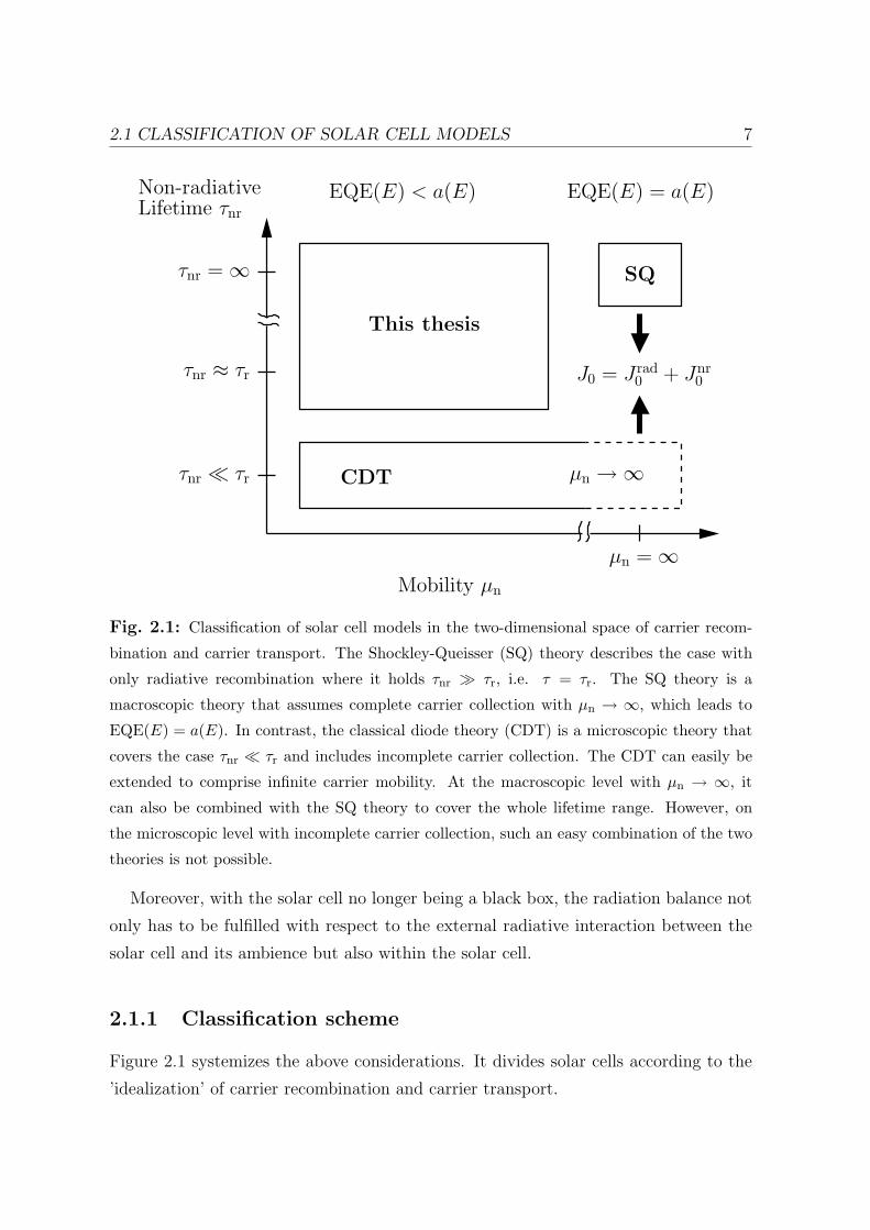
Non-radiativeLifetime τnr
SQ
CDT µn →∞τnr ¿ τr
τnr ≈ τr
τnr = ∞
µn = ∞
This thesis
Mobility µn
J0 = J rad0 + Jnr
0
EQE(E) < a(E) EQE(E) = a(E)
Fig. 2.1: Classification of solar cell models in the two-dimensional space of carrier recom-
bination and carrier transport. The Shockley-Queisser (SQ) theory describes the case with
only radiative recombination where it holds τnr À τr, i.e. τ = τr. The SQ theory is a
macroscopic theory that assumes complete carrier collection with µn → ∞, which leads to
EQE(E) = a(E). In contrast, the classical diode theory (CDT) is a microscopic theory that
covers the case τnr ¿ τr and includes incomplete carrier collection. The CDT can easily be
extended to comprise infinite carrier mobility. At the macroscopic level with µn → ∞, it
can also be combined with the SQ theory to cover the whole lifetime range. However, on
the microscopic level with incomplete carrier collection, such an easy combination of the two
theories is not possible.
Moreover, with the solar cell no longer being a black box, the radiation balance not
only has to be fulfilled with respect to the external radiative interaction between the
solar cell and its ambience but also within the solar cell.
2.1.1 Classification scheme
Figure 2.1 systemizes the above considerations. It divides solar cells according to the
’idealization’ of carrier recombination and carrier transport.

8 CHAPTER 2. EFFICIENCY LIMITS OF SOLAR CELLS
With respect to recombination, the ideal case is reached, when carriers only re-
combine radiatively. The crucial parameter for recombination is the minority carrier
lifetime, which consists of a radiative lifetime τr and a lifetime τnr for non-radiative
processes and is computed with 1/τ = 1/τr + 1/τnr.
The second dimension is the dimension of carrier transport as expressed by the
minority carrier mobility µn. Ideally, µn is infinity. Then, the spatial resolution of the
solar cell becomes obsolete, since all generated carriers are collected independent of the
position of the generation. In this case, a macroscopic solar cell model is sufficient to
describe the cell’s efficiency.
The ideal carrier transport also makes a spatial resolution of carrier generation
unnecessary. The solar cell is completely defined by macroscopic quantities, such as
the absorptance spectrum a(E), where E is the photon energy.
As a consequence of the infinite mobility, the probability to collect an absorbed
photon under short circuit conditions becomes unity. Therefore, the external quan-
tum efficiency EQE(E) as defined by the number of collected electrons divided by the
number of incident photons under short circuit conditions equals the absorptance a(E).
Non-ideal transport requires a spatial resolution in the direction of current transport.
The macroscopic approach has to be replaced by a microscopic approach that includes
the spatial resolution of carrier generation, recombination, and transport. Not all
absorbed photon are collected and it holds EQE(E) < a(E).
The SQ theory assumes only radiative recombination, i.e. τ = τr, and also complete
carrier collection, i.e. µn →∞. Conversely, the classical diode theory (CDT) is suited
for solar cells with non-ideal recombination and non-ideal carrier collection. While
the diode theory can easily be extended to comprise complete carrier collection, such
an extension is not so straightforward when recombination is dominated by radiative
recombination.
The existing theories are well equipped to describe the case of complete carrier
collection, where the solar cell is only described as a black box with macroscopic prop-
erties. However, they fail to describe the combination of incomplete carrier collection
with radiative recombination.
In the following, I recapitulate the SQ theory and the diode theory. The next chapter
will then address the task of providing the missing link between the theories.

2.2 CURRENT-VOLTAGE CHARACTERISTIC OF SOLAR CELLS 9
2.2 Current-voltage characteristic of solar cells
Throughout this thesis, all solar cells are considered ideal insofar that their series
resistance is zero and their parallel resistance is infinity. Therefore, they exhibit the
current/voltage characteristic
J(V ) = J0
(exp
(qV
kBT
)− 1
)− Jsc, (2.1)
where J0 is the saturation current density and Jsc is the short circuit current density.
The applied voltage is V , q is the elementary charge, kB is Boltzmann’s constant, and
T is the absolute temperature.
From the saturation current J0 and the short circuit current Jsc one obtains the
open circuit voltage
Voc =kBT
qln
(Jsc
J0
+ 1
), (2.2)
the fill factor with the phenomenological expression [12]
FF =uoc − ln (uoc + 0.72)
uoc + 1(2.3)
with uoc = qVoc/(kBT ), and the efficiency
η =qJscVocFF
Pin
, (2.4)
where Pin is the areal power density of the illumination. Throughout this thesis I use
the global AM1.5g spectrum scaled to Pin = 100 mW/ cm2 from Ref. [13].
2.3 Radiative efficiency limit
This section discusses the maximum power conversion efficiency of a single junction
solar cell, as determined by the detailed radiation balance between the solar cell and
its ambience. This maximum efficiency is called detailed balance efficiency limit or
radiative efficiency limit. In the radiative efficiency limit, radiative recombination is
the only loss mechanism. As will be shown below, such radiative recombination cannot
be circumvented.
Section 2.3.1 analyzes the radiative efficiency limit of solar cells with infinite mo-
bility and the resulting consequences as described above. Section 2.3.2 discusses the
implications of a non-ideal quantum efficiency for the detailed balance efficiency, which
constitutes the basis for the detailed analysis presented in chapter 3.

10 CHAPTER 2. EFFICIENCY LIMITS OF SOLAR CELLS
Jel
ΦemΦsun Φbb
Solar cell
Φsun − Φabssun Φbb − Φabs
bb
Fig. 2.2: Sketch of a solar cell as seen by Shockley and Queisser. The cell is a black box
with complete carrier collection. Internal processes are not accounted for. Only the external
radiation fluxes and the electrical current drawn from the cell are considered. From the
incoming solar radiation Φsun and the ambient black body irradiation Φbb only the fluxes
Φabssun and Φabs
bb are absorbed. The rest is transmitted (or rather: reflected, since the back side
is perfectly reflected). The absorbed fluxes are balanced by the voltage-dependent emission
flux Φem and the electrical current Jel.
2.3.1 Complete carrier collection
As it turns out, the absorptance spectrum a(E) of the solar cell, where E is the the
photon energy, is the crucial material characteristic that determines the solar cell’s
radiative efficiency limit. In this section, I recapitulate the case of a solar cell with
homogenous material parameters, in particular a homogeneous band gap energy Eg,
which ideally results in a step like absorptance function. Appendix A presents the
influence of lateral fluctuations of the band gap energy, which cause a broadening of
the absorption spectrum, on the radiative efficiency limit. It also discusses the existence
of an optimal absorptance spectrum that would result in an ultimate efficiency limit
for a given irradiation spectrum.
Homogeneous band gap
The maximum power conversion efficiency of a solar cell with homogeneous band gap
is given by the radiative recombination limit and depends only on the cell temperature,
the spectral distribution of the solar irradiation, and on the band gap energy Eg of the
semiconductor acting as the photovoltaic absorber material. This theoretical efficiency
limit was initially presented by Shockley and Queisser [10] and consists of a very much

2.3 RADIATIVE EFFICIENCY LIMIT 11
idealized thermodynamic approach that is based on the detailed balance between the
radiation fluxes absorbed and emitted by the solar cell. Geometrical extensions as well
as optical and electrical material parameters are not accounted for. The solar cell is
regarded as a black box, and only external radiation fluxes and currents are balanced
as sketched in Fig. 2.2.
The ideal solar cell is completely characterized by its absorptance a(E) expressed
by the Heavyside function
a(E) =
1, E ≥ Eg
0, E < Eg,(2.5)
where E is the photon energy.
From this starting point Shockley and Queisser based their derivation of the radiative
efficiency limit on four basic assumptions:
(i) All photons with energy larger than the band gap Eg are completely absorbed
and generate one electron/hole pair each.
(ii) Under short circuit conditions all photo-generated carriers are collected and con-
tribute to the photocurrent Jsc.
(iii) Spontaneous emission of photons by radiative recombination of electron/hole
pairs is the only loss mechanism as required by the principle of detailed balance.
(iv) All photons emitted by radiative recombination have the same chemical potential
µ.
Hidden within these four assumptions are two important aspects. Assumption (i) im-
plicitly requires virtually infinite thickness of the photovoltaic absorber and assumption
(ii) and (iv) require virtually infinite mobility of the photogenerated minority carriers.
Given the above assumptions, Shockley and Queisser now calculate the saturation cur-
rent J0 of the solar cell from the thermodynamic equilibrium in the dark and compute
the short circuit current Jsc from the irradiating solar spectrum. They therewith ar-
rive at the current/voltage characteristic of the solar cell from which they derive the
conversion efficiency. In this section I recapitulate these calculations.
The fundamental starting point for the calculation of the SQ efficiency limit is the
principle of detailed balance, which states that in thermodynamic equilibrium, every
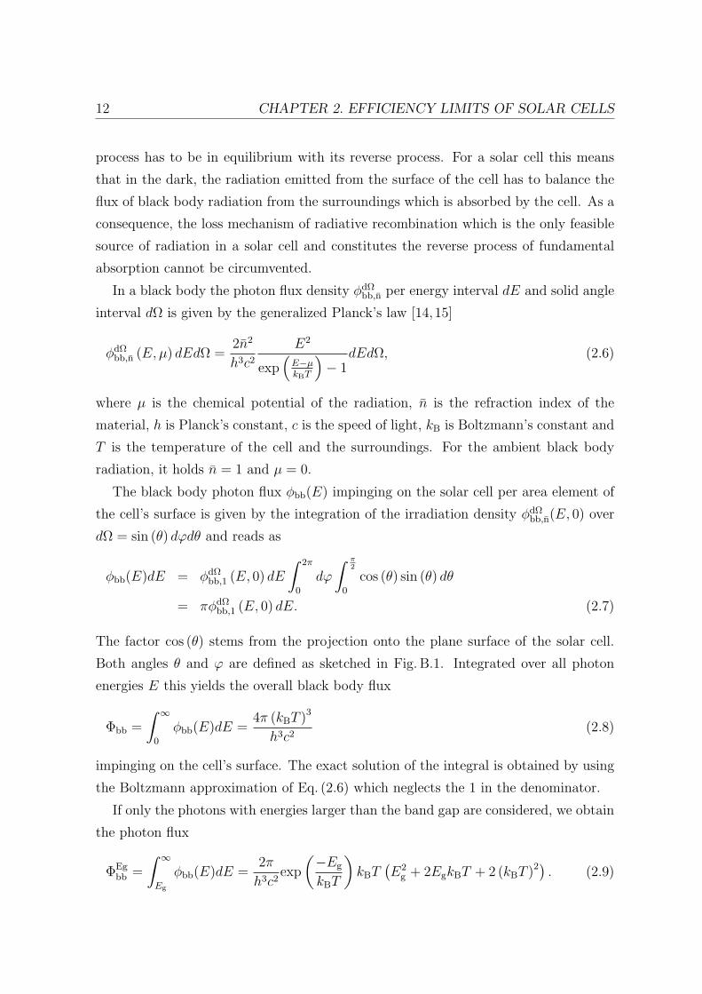
12 CHAPTER 2. EFFICIENCY LIMITS OF SOLAR CELLS
process has to be in equilibrium with its reverse process. For a solar cell this means
that in the dark, the radiation emitted from the surface of the cell has to balance the
flux of black body radiation from the surroundings which is absorbed by the cell. As a
consequence, the loss mechanism of radiative recombination which is the only feasible
source of radiation in a solar cell and constitutes the reverse process of fundamental
absorption cannot be circumvented.
In a black body the photon flux density φdΩbb,n per energy interval dE and solid angle
interval dΩ is given by the generalized Planck’s law [14,15]
φdΩbb,n (E, µ) dEdΩ =
2n2
h3c2
E2
exp(
E−µkBT
)− 1
dEdΩ, (2.6)
where µ is the chemical potential of the radiation, n is the refraction index of the
material, h is Planck’s constant, c is the speed of light, kB is Boltzmann’s constant and
T is the temperature of the cell and the surroundings. For the ambient black body
radiation, it holds n = 1 and µ = 0.
The black body photon flux φbb(E) impinging on the solar cell per area element of
the cell’s surface is given by the integration of the irradiation density φdΩbb,n(E, 0) over
dΩ = sin (θ) dϕdθ and reads as
φbb(E)dE = φdΩbb,1 (E, 0) dE
∫ 2π
0
dϕ
∫ π2
0
cos (θ) sin (θ) dθ
= πφdΩbb,1 (E, 0) dE. (2.7)
The factor cos (θ) stems from the projection onto the plane surface of the solar cell.
Both angles θ and ϕ are defined as sketched in Fig. B.1. Integrated over all photon
energies E this yields the overall black body flux
Φbb =
∫ ∞
0
φbb(E)dE =4π (kBT )3
h3c2(2.8)
impinging on the cell’s surface. The exact solution of the integral is obtained by using
the Boltzmann approximation of Eq. (2.6) which neglects the 1 in the denominator.
If only the photons with energies larger than the band gap are considered, we obtain
the photon flux
ΦEgbb =
∫ ∞
Eg
φbb(E)dE =2π
h3c2exp
(−Eg
kBT
)kBT
(E2
g + 2EgkBT + 2 (kBT )2) . (2.9)

2.3 RADIATIVE EFFICIENCY LIMIT 13
The black body photon flux absorbed by the solar cell is given by the integration of
the irradiation density φdΩbb,n(E, 0) over dE and dΩ = sin (θ) dϕdθ and reads as1
Φabsbb =
∫ ∞
0
a (E) φdΩbb,n (E, 0) dE
∫ 2π
0
dϕ
∫ θc
0
cos (θ) sin (θ) dθ
=
∫ ∞
0
a (E) φbb(E)dE. (2.10)
Due to Snellius’ law of refraction the half sphere outside of the cell will be mapped
onto the cone with critical angle θc = arcsin (1/n). Therefore, the interaction between
cell and surroundings only affects radiation (inside the cell) within angles smaller than
θc.2 For the step function Eq. (2.5) we find Φabs
bb = ΦEgbb .
With the equilibrium emission current Φem(V = 0) in the dark being equal to the
absorbed black body radiation ΦEgbb from the ambience we obtain from Eq. (2.10) the
emission current under short-circuit conditions with V = 0. Next, we need to derive the
current voltage dependence of the emission current. Whereas the chemical potential of
the emitted photons is µ = 0 in thermal equilibrium, it holds µ = EFn − EFp > 0 if a
voltage V is applied or if the cell is illuminated. Here, EFn and EFp are the quasi-Fermi
levels for electrons and holes respectively. Under the assumption that the mobility µn
of the minority carriers is large enough to guarantee that all carrier gradients will
immediately be levelled out, µ is constant throughout the cell and equal to the applied
voltage qV . This means that all photons emitted by radiative recombination have
the same chemical potential µ = qV (assumption (iv)). Therewith and by using the
Boltzmann approximation of Eq. (2.6) which is valid for E − µ À kT , the emission
current caused by radiative recombination is given by
Φem (V ) = π
∫ ∞
0
a (E) φdΩbb,1 (E, V ) dE ≈ ΦEg
bbexp
(qV
kBT
). (2.11)
Next, we consider the solar cell under illumination and compute the electrical current
Jsc under short-circuit conditions. The solar irradiation impinges vertically on the solar
cell surface with an integrated photon flux density
Φsun =
∫ ∞
0
φsun(E)dE, (2.12)
1Note that throughout this thesis I assume a perfectly reflecting back side which means that
radiative interaction is limited to the front surface. Note also that all fluxes are denoted as particle
flux densities per unit area ( cm−2 s−1)2Note the equivalence of either integrating φdΩ
bb,1(E, 0) from θ = 0 to π/2 outside the cell surface
or integrating φdΩbb,n(E, 0) from θ = 0 to θc inside the cell.

14 CHAPTER 2. EFFICIENCY LIMITS OF SOLAR CELLS
where φsun(E) is the spectral density of the solar spectrum. In analogy to Eq. (2.9), I
define the photon flux ΦEgsun which includes all photons with an energy larger than the
band gap.
For a step-function absorptance, all photons with energies E ≥ Eg are being ab-
sorbed and generate one electron/hole pair each regardless of any surplus energy (as-
sumption (i)). The absorbed photon flux Φabssun is equal to ΦEg
sun. From balancing in-
coming and outgoing photon fluxes and the electrical current under short-circuit con-
ditions as depicted in Fig. 2.2, it holds for the electrical current Jel(V = 0) = Jsc =
ΦEgsun + ΦEg
bb − Φem(V = 0), i.e. Jsc = ΦEgsun. This means that under short-circuit con-
ditions all excess carriers are completely collected and contribute to the current Jsc
(assumption (ii)).
Balancing incoming and drawn off currents for V 6= 0 leads to the current/voltage
characteristic
Jel (V ) = ΦEgsun + ΦEg
bb − Φem (V ) = ΦEgsun − ΦEg
bb
(exp
(qV
kBT
)− 1
), (2.13)
with the short circuit current Jsc = ΦEgsun and the saturation current J0 = ΦEg
bb (cmp.
Eq. (2.1). Note again that all currents are denoted as particle currents and have to be
multiplied with the elementary charge q to obtain electrical currents.
2.3.2 Incomplete carrier collection
When transport is non-ideal, the quantum efficiency no longer equals the absorptance.
The short-circuit current is given by
Jsc =
∫ ∞
0
EQE(E)φsun(E)dE. (2.14)
As Rau shows in his disquisition on the reciprocity between photovoltaic quantum
efficiency and electroluminescent emission of solar cells [16], the excess emission current
caused by radiative recombination reads as
Φem (V )− ΦEgbb =
∫ ∞
0
EQE (E) φbb(E)dE
exp
(qV
kBT
)− 1
. (2.15)
In analogy to Eq. (2.13), the short circuit and the emission current yield the cur-
rent/voltage characteristic of the solar cell.
There exists no closed-form expression for the quantum efficiency EQE. Therefore,
the next chapter derives a numerical computation scheme.

2.4 CLASSICAL DIODE THEORY 15
2.4 Classical diode theory
2.4.1 Incomplete carrier collection
Shockley’s and Queisser’s detailed balance considerations give the overall efficiency
limit for any single band gap material in dependence of the semiconductor’s band gap
Eg. They do not take into account geometrical extensions and either incomplete absorp-
tion or incomplete carrier collection. A real solar cell is far from being perfect though.
Therefore, it has to be treated differently. In this section, the cell is still ideal insofar as
there are no parasitic Ohmic losses. I will consider an abrupt one-sided pn+-junction
where I also neglect absorption and recombination in either emitter or space-charge
region. Non-idealities are expressed by finite mobility µn of the minority carriers (in
our case electrons), by the finite absorptance of the cell in terms of cell thickness d and
absorption coefficient α and by non-radiative recombination mechanisms as expressed
by the lifetime τ .
In contrast to the SQ efficiency limit the following classical derivation of the diode
equation is based on charge carrier transport or, more precisely, diffusive minority
carrier transport in the quasi-neutral base region of the absorber material. To describe
the current/voltage characteristic of an abrupt one-sided pn-junction under low-level
injection conditions with n(x) ¿ p(x) ≈ NA, one has to solve the diffusion equation [17]
Dnd2n
dx2− n− n0
τ= −Gsun (x) (2.16)
for the minority carriers (electrons for p-type doped samples) in the quasi-neutral base
of the device with the boundary conditions
n (x = 0) = n0exp
(qV
kBT
)(2.17)
at the edge of the space charge region (x = 0) and
dn
dx
∣∣∣∣∣x=d
=−Sn
Dn
(n (x = d)− n0) (2.18)
at the back contact (x = d). Here, Dn = (kBT/q)µn is the electron diffusion constant, τ
is the electron lifetime and Sn is the electron recombination velocity at the back contact
(which ideally equals zero). Also, n0 = n2i /NA is the electron concentration in thermal
equilibrium where ni is the intrinsic carrier concentration and NA is the doping density.

16 CHAPTER 2. EFFICIENCY LIMITS OF SOLAR CELLS
Carriers are generated by external excitation with the generation rate Gsun(x) and
recombine with the (low level injection) recombination rate R = (n−n0)/τ . Calculating
the current Jel (V ) = Dndn/dx at x = 0 yields the current/voltage characteristic
Jel (V ) = Jsc − J0
(exp
(qV
kBT
)− 1
)(2.19)
where with Sn = 0, J0 is given by
J0 =Dnn0
Ln
1− 2
1 + exp(
2dLn
) =
Dnn0
Ln
tanh
(d
Ln
). (2.20)
Here, Ln =√
Dnτ is the diffusion length of the minority carriers.
The short-circuit current Jsc depends on the generation profile Gsun(x). For a thick
cell with d À 1/α(E), where α(E) is the absorption coefficient, the easiest approach
is [18]
Gsun(x,E) = φsun(E)α(E)exp (−α(E)x) , (2.21)
where φsun(E) is the incident photon flux. With Sn = 0 we obtain
Jsc =
∫ ∞
0
φsun(E)αLn
1− α2L2n
1− αLn + 2
αLnexp (−αd)− exp(−dLn
)
exp(
dLn
)+ exp
(−dLn
) dE
=
∫ ∞
0
φsun(E)αLn
1− α2L2n
tanh
(d
Ln
)− αLn +
αLnexp (−αd)
cosh(
dLn
) dE. (2.22)
2.4.2 Complete carrier collection
In the case of ideal transport with µn → ∞, the derivations of the previous section
simplify significantly. Under short circuit conditions, all absorbed photons are collected
and the short circuit current
Jsc =
∫ ∞
0
(1− exp (−αd)) φsun(E)dE =
∫ ∞
0
a(E)φsun(E)dE = JSQsc (2.23)
is equal to the maximum achievable short circuit current JSQsc .
For the non-radiative recombination current, the high mobility limit reads as
Jnr0 =
n0d
τnr
. (2.24)
2.4 CLASSICAL DIODE THEORY 17
If the non-radiative lifetime is comparable to the radiative lifetime then the overall
recombination current is the sum of non-radiative and radiative recombination current
according to J0 = Jnr0 + J rad
0 , where J rad0 is given by Eq. (2.9). Note that this simple
summing up of the recombination currents is only applicable in the limit of complete
carrier collection with µn →∞. Otherwise, the spatially resolved recombination rates
have to be added up, which is accomplished by adding up the inverse lifetimes. For
the solution of the diffusion equation Eq. (2.16), this adding up of the inverse lifetimes
does not lead to a simple linear superposition of the recombination currents, as can be
verified by looking at Eq. (2.20).
And besides, at this point, microscopic detailed balance arguments come into play,
which brings us to the elaborated model presented in the next chapter.

Chapter 3
Generalized efficiency limit
Abstract: This chapter presents a self-consistent model that combines charge
carrier transport and detailed radiation balances to describe the efficiency of solar
cells in the whole range of non-radiative and radiative recombination as well as
complete and incomplete carrier collection. An extra generation term accounting
for the absorption and reemission of photons emitted by radiative recombination
(photon recycling) is incorporated into the diffusion equation, thereby fulfilling
internal and external radiation balances. The chapter shows that if the minority
carrier mobility drops below a critical mobility then the solar cell efficiency is
reduced drastically even in the otherwise most ideal case. It presents an analytical
approximation of the numerical model. After having discussed the hypothetical
case of an energy-independent absorption coefficient, the model is extended to
energy-dependent light absorption and applied to experimental absorption data
of crystalline silicon, amorphous silicon, and Cu(In,Ga)Se2. While for crystalline
silicon, transport is not a limiting factor, solar cells made of amorphous silicon
or Cu(In,Ga)Se2 need to utilize built-in electric fields or band gap grading to
enhance carrier collection. Amorphous silicon comes close to having an inherent
mobility problem even in the radiative recombination limit.
Based on the considerations presented in the previous chapter, this chapter develops
a generalized model that combines the SQ theory with the classical diode theory by
incorporating the detailed radiation balance of absorbed and emitted photons into a
microscopic transport approach.
18

3.1 RADIATIVE RECOMBINATION AND PHOTON RECYCLING 19
3.1 Radiative recombination and photon recycling
Understanding the interaction between photons and electrons inside a semiconductor
begins with fundamental light absorption. A photon is absorbed by exciting a valence
electron into the conduction band, thereby creating an electron/hole pair. After a
certain time, this electron/hole pair will recombine again, thereby dispensing its surplus
energy either in form of phonons to the crystal lattice (non-radiative recombination) or
by emitting a photon (radiative recombination). Non-radiative recombination would
lead to an increase in the cell temperature, were it not for the assumed perfect thermal
coupling to the surroundings which act as an ideal heat sink. With such perfect thermal
coupling, however, the surplus energy is simply transferred to the ambience in form of
heat. It is irretrievably lost for the utilization of electrical energy.
In contrast, radiative recombination is not such a simple one-step mechanism. Dur-
ing the radiative recombination of an electron/hole pair, a photon is spontaneously
emitted into an arbitrary direction. This photon is either emitted through the surface
of the cell or it is reabsorbed along its path within the solar cell. In the latter case, it
generates an additional electron/hole pair, which in turn can again recombine radia-
tively and emit another photon. The repeated absorption and emission of photons is
called photon recycling (PR). As will be shown in this chapter, the photon recycling
process supplies the missing link between the SQ theory and the classical diode theory.
It is the basis for the internal and external radiation balances.
Furthermore, the additional generation rate caused by reabsorbed photons effec-
tively decreases the loss of carriers caused by radiative recombination. Radiatively
recombining carriers are only lost if they recombine close to the surface. Deep within
the bulk material they are completely recycled and therefore not lost at all. As a con-
sequence, the internal generation caused by photon recycling leads to an increase in
cell efficiency when compared to the case without photon recycling.
After surveying the treatment of the photon recycling effect in the literature, quan-
tifying the internal generation rate will be the main element in the model developed in
section 3.3.

20 CHAPTER 3. GENERALIZED EFFICIENCY LIMIT
3.2 Photon recycling in the literature
The effect of photon recycling (PR) was first addressed by Dumke [19], Moss [20], and
Landsberg [21] as early as 1957. Dumke was already aware of the fact that the PR
would lead to an infinite radiative lifetime deep in the bulk. He also pointed out the
relevance of photonic transport in addition to electron transport.
First experimental evidence of the PR effect was reported another 10 years later
in the late 1960ies and early 1970ies. As was to be expected, the effect gained im-
portance in direct semiconductors with low radiative and high non-radiative lifetimes
such as GaAs that were used for optoelectronic devices. Carr [22] and later Carr and
Kameda [23] discovered PR effects in luminescence measurements with GaAs sam-
ples and termed them ’self-excitation’. Hwang [24] found reabsorption of photons to
influence the quantum efficiency of radiative recombination determined in photolumi-
nescence experiments with heavily doped GaAs. Stern and Woodall [25] were the first
to introduce the denotation ’photon recycling’. They found PR effects to reduce the
threshold current of GaAs double-heterostructure lasers by roughly 20 %.
The first rigorous theoretical treatment was presented in 1977 by Kuriyama et al. [26]
who used their theory to analyze quantum efficiencies and diffusion lengths in AlGaAs
heterostructures. Whereas previously, small quantum efficiencies [27] and large surface
recombination velocities [24] had led to a domination of non-radiative recombination
which made the treatment of PR effects superfluous, the development of higher quality
crystals now required the consideration of photon recycling. Analysis without the
consideration of PR yielded obviously false internal quantum efficiencies and, thus,
made a detailed theoretical treatment indispensable.
Despite being the first treatment of PR, the publication of Kuriyama et al. [26] still
remains the basis for virtually all following publications. Additionally to providing
the theoretical treatment to compute the internal generation rate caused by radiative
interaction within the semiconductor, they also developed an iterative scheme to solve
the integro-differential equation resulting from the formulation of the problem, which is
still widely used amongst scholars working on the topic. Using the fundamental system
of the homogeneous solution they compute the contribution of each reabsorption cycle
from the previous carrier profile. The initial profile is obtained from the analytical
solution without PR.

3.2 PHOTON RECYCLING IN THE LITERATURE 21
Almost simultaneously, Asbeck [28] derived a (numerical) expression for a modi-
fied radiative lifetime that includes reabsorption of photons. Mettler [29] modified
Kuriyama’s rather complex derivation with cylindrical coordinates, and developed the
approach also used in this thesis.
Following publications extended the treatments to include, for instance, graded band
gaps [30,31], transient effects [32–35], optical modulation [36], pin structures [37], and
two-dimensional effects [38].
Various procedures have been proposed for the mathematical formulation of the
problem. For perfect optical confinement, an infinite spatially periodic continuation
of the problem allows for an anharmonic Fourier analysis [39]. Also, perturbational
and variational methods have been developed [40–42]. However, these mathematically
more sophisticated approaches suffer from their limited applicability arising from the
dependence of the PR effect on device geometry, energy dependencies, and operating
conditions.
Special emphasis was placed on analytical approximations that allowed for incor-
porating the PR effect as modified lifetime and diffusion constant into the classical
diffusion equation [40, 43–50]. These approaches and either their usefulness or the
potential conflicts with respect to the detailed balance principle will be discussed sep-
arately in section 3.7.1 in the context of developing analytical approximations for the
solar cell efficiency.
Most of the above publications dealt with light emitting diodes and lasers and the
role of photon recycling for the experimental determination of lifetimes and quantum
efficiencies. The relevance of PR for solar cells was not investigated until 1991 when
Parrott [51] and Durbin and Gray [52] presented simulations of solar cell efficiencies
at the 22nd IEEE PVSEC conference. In a further publication [53], Durbin and Gray
refined their numerical model. They investigated the influence of photon recycling on
the efficiency of solar cells but restrained themselves to the practical cases with non-
radiative recombination being the dominant recombination process. A similar focus was
also chosen by Badescu and Landsberg [54], Yamamoto et al. [55], and Balenzategui
and Martı [56].
Parrott [57] was the first to relate photon recycling and the detailed balance effi-
ciency limit of Shockley and Queisser. However, while deriving his model for spatially
dependent chemical potential of the emitted photons, all his computations are carried
22 CHAPTER 3. GENERALIZED EFFICIENCY LIMIT
out under the assumptions that the chemical potential is constant within one absorp-
tion length. Especially for low mobilities and for the relevant energy range close to the
band gap, where the absorption coefficient is very small, this approximation is rather
crude.
The objective of this thesis is to provide a detailed and, particularly important,
self-consistent model that combines the diffusion equation with the detailed balance
approach. Special emphasis is placed on finite carrier transport in the radiative ef-
ficiency limit and the interplay between photon recycling and the detailed balance
principle. This approach differs from most other contributions in the literature insofar
as the detailed radiation balances provide a relentless limit that imposes strict checks
for the numerical accuracy of the computations. For instance, these radiation balance
checks call for the self-consistent averaging of all generation rates, thereby warranting
the conservation of particles1. In the practical cases discussed in the vast variety of the
literature, these strict conditions were not imposed. On the one hand this greatly sim-
plified the equations entering in the numerical model but on the other hand deprived
the model of an accuracy check that - with regard to the complexity of the equations
- might prove utterly necessary to guarantee the accuracy of the obtained results.
3.3 Diffusion equation with reabsorption
This section tackles the task of incorporating the photon recycling effect into a micro-
scopic transport approach. The starting point will be the classical diode theory, i.e.
the minority carrier diffusion equation (2.16), which is valid under low-level injection
conditions. The photon recycling leaves everything unchanged except for an additional
generation term caused by reabsorbed photons.
For the mathematical treatment of the photon recycling effect, a one-dimensional
description of electron transport is still sufficient but has to be complemented by the
three-dimensional emission of photons by recombining electron/hole pairs. Photons
emitted by radiative recombination which are reabsorbed cause an extra generation of
carriers. The diffusion equation (2.16) is extended to
Dnd2n
dx2+ Gint (x)− n
τr
− n− n0
τnr
= −Gsun (x)−Gbb (x) , (3.1)
1In the literature, such averaging was only performed by Durbin and Gray [53].

3.3 DIFFUSION EQUATION WITH REABSORPTION 23
1
2
3
4
(b) Textured(a) Plane
Fig. 3.1: In a solar cell with plane surface (a) all external rays impinging on the front
surface are refracted towards the surface normal due to the higher refractive index n inside
the semiconductor. Internally emitted rays leave the cell if the emission angle is smaller than
the critical angle θc = arcsin (1/n) (ray 1). If the emission angle is larger than θc then the
ray is internally reflected until it is completely absorbed within the solar cell (ray 2). In a cell
with textured surface (b) an external ray is randomized upon transmitting the front surface.
The same accounts for internally emitted rays. These internal rays are transmitted with the
transmission probability tlamb (rays 3) and reflected with the probability 1− tlamb (rays 4).
where recombination is split up into radiative recombination with the radiative lifetime
τr and non-radiative recombination with the non-radiative lifetime τnr. The external
generation consists of the equilibrium black body generation rate Gbb and the non-
equilibrium solar generation rate Gsun. The extra internal generation is accounted for
by adding the internal generation rate
Gint (xg) =
∫ xr=d
xr=0
δGint (xg, xr) = const
∫ d
0
fr(xg, xr)n(xr)dxr (3.2)
caused by radiative recombination throughout the sample. Here, δGint(xg, xr) denotes
the generation rate at x = xg that is caused by radiatively recombining carriers in the
incremental plain xr < x < xr + δxr. As will be shown in appendix B, δGint(xg, xr) de-
pends on the electron concentration at xr and the optical interaction function fr(xg, xg).
To obtain the overall internal generation rate at x = xg one has to integrate over all
possible recombination events, that is over the whole thickness of the solar cell from
xr = 0 to xr = d. For all terms that include light reflection at or light transmission
through the front surface of the solar cell, the nature of the front surface has to be
considered as well. As sketched in Fig. 3.1, I distinguish two cases, namely (a) a plane
and (b) a textured front surface.
The detailed derivation of the model is provided in appendix B. The appendix starts

24 CHAPTER 3. GENERALIZED EFFICIENCY LIMIT
by reformulating the diffusion equation as a linear matrix equation based on linear op-
erators. Then it gives expressions for the transport operator and the recombination
operator. Subsequently, it derives an expression for the internal generation rate, start-
ing with the direct radiative interaction between two locations in the cell, and followed
by the inclusion of multiple reflections. Finally, it derives expressions for the external
generation rates Gbb and Gsun caused by black body and solar irradiation respectively.
3.3.1 Parameter normalization
The major difference between the Shockley-Queisser detailed balance treatment and
the considerations of the preceding section is, that non-ideal phenomena in terms of
optical absorption and electrical transport can be analyzed with the latter approach.
The analysis is not restricted to infinite mobility and complete absorption anymore as
it had been in the SQ theory. Now the solar cell features the finite thickness d, the
absorption coefficient α, the minority carrier mobility µn, the doping density NA, and
the non-radiative lifetime τnr.
In the following sections I investigate the influence of these device and material
parameters on the saturation current J0 and the short circuit current Jsc, and conse-
quently on the power conversion efficiency η. To obtain Jsc, I solve the matrix equation
obtained from the discretization of Eq. (3.3) performed in appendix B with illumination
for the boundary conditions V = 0 at x = 0. Subsequently, I solve the matrix equation
without illumination for V = (kBT/q) ln (2) at x = 0 to obtain J0. From Jsc and J0 I
obtain the open-circuit voltage, the fill factor and the efficiency in dependence of µnorm
and Eg (cf. section 2.2).
In order to facilitate the analysis of the influence of the different parameters, I sum
up several quantities in normalized parameters. To investigate the influence and mutual
interplay of these parameters, it is convenient to introduce the normalized length ξ =
α0x, where α0 = α (E = Eg + kBT ) is the absorption coefficient at a photon energy
Eg + kBT . The electron concentration is normalized to ν = n/n0 with n0 = n2i /NA
being the equilibrium electron concentration that in turn depends on the intrinsic
carrier concentration ni and the doping density NA. Additionally, I normalize the
photon fluxes on the black body flux ΦEgbb as defined in Eq. (2.9).

3.3 DIFFUSION EQUATION WITH REABSORPTION 25
By dividing Eq. (3.1) by α0ΦEgbb one obtains the dimensionless equation
µnormd2ν
dξ2+ γint (ξ)− ν (ξ) (1 + ϑr)
τ rnorm
= −γsun (ξ)− γbb (ξ)− ϑr
τ rnorm
(3.3)
with ϑr = τr/τnr and with the dimensionless rates γi = Gi/(α0Φ
Egbb
). All dependencies
on α0, µn and NA are summed up in the normallized mobility
µnorm =µ
µref
(3.4)
with the reference mobility
µref =qΦEg
bb
kBTα0n0
=q2πNA
(E2
g + 2EgkBT + 2 (kBT )2)
h3c2NCNVα0
. (3.5)
Here, I used n2i = NCNVexp (−Eg/(kBT )) with NC and NV being the effective densi-
ties of states in the conduction and the valence band respectively. With τr given by
Eq. (B.21), the normalized lifetime
τ rnorm =
α0ΦEgbbτr
n0
=α0Φ
Egbb
R0
=α02πexp
(−Eg
kBT
)kBT
(E2
g + 2EgkBT + 2 (kBT )2)
h3c2∫∞
Egα (E) 4πφdΩ
bb,n (E, 0) dE(3.6)
and the dimensionless rates γi only depend on the band gap Eg and on the functional
dependence of the absorption coefficient α(E) on the energy E as listed in Tab. 3.2.
• For an energy-independent absorption coefficient α = α0 for E ≥ Eg and α = 0
for E < Eg it holds R0 = 4α0n2ΦEg
bb (cf. Eq. (2.9) and Eq. (B.19)) and therewith
τ rnorm(const) =
1
4n2. (3.7)
• With α(E) = α0
√(E − Eg)/kBT for a direct semiconductor we obtain the Boltz-
mann approximation of the normalized lifetime
τ rnorm(direct) =
4(E2
g + 2EgkBT + 2 (kBT )2)√
πn2(4E2
g + 12EgkBT + 15 (kBT )2) ≈1√πn2
(3.8)
• In an indirect semiconductor it holds α(E) = α0 (E − Eg)2 /(kBT )2 and therewith
we obtain the normalized lifetime
τ rnorm(indirect) =
E2g + 2EgkBT + 2 (kBT )2
4n2(E2
g + 6EgkBT + 12 (kBT )2) ≈1
4n2(3.9)

26 CHAPTER 3. GENERALIZED EFFICIENCY LIMIT
The approximations in the previous equations (3.8) and (3.9) are valid as long the
band gap Eg is larger than the thermal energy kBT , which is the case for semiconductors
commonly used for solar cells with Eg > 1 eV and kBT = 26 meV at room temperature.
In all three cases the generation rates γi are independent of α0 as well. Thus, only
the functional dependence of the absorption coefficient on the energy influences the
normalized generation profiles.
For the electrical current
Jel = Dndn
dx= µnormΦEg
bb
dν
dξ(3.10)
only the normalized mobility µnorm is relevant and therefore also the efficiency only
depends on the normalized lifetime and normalized mobility.
This result shows that in the ideal case where radiative recombination is the only
loss mechanism, it is impossible to distinguish between the influence of the optical
absorption in terms of α0 and the influence of the minority carrier mobility µn for a
given normalized thickness d/α0 and given front and back side reflectivities. Only the
product µnα0 is relevant for the achievable efficiency. In the non-ideal case of non-
radiative recombination however, electrical and optical effects can be separated. This
will be described below in section 3.4.2. The repeated emission and reabsorption of
photons causes an effective optical transport of charge carriers. The fact that only the
product µnα0 is important for the current-voltage characteristic of the device shows
the virtual equivalence of optical and electrical carrier transport.
3.3.2 Free parameters
As a consequence of the normalization, the number of parameters is reduced and the
only free parameters in the model are
(i) the band gap energy Eg,
(ii) the normalized mobility µnorm = µ/µref ,
(iii) the normalized thickness α0d,
(iv) the nature (textured or plane) of the front surface,
(v) the lifetime ratio ϑr of radiative and non-radiative lifetime, and

3.4 RESULTS WITH CONSTANT ABSORPTION COEFFICIENT 27
Tab. 3.1: Standard parameters used for the computations of the reabsorption scheme.
Eg n d %f %b Sn α(E) front surface
1 eV 3 10/α0 0 1 0 α0 textured
(vi) the energy-dependence of the absorption coefficient α(E) (constant, square root,
parabolic).
All discussions are first performed for the theoretical case with constant absorption
coefficient to emphasize fundamental dependencies. Afterwards, I discuss the cases of
direct and indirect semiconductors. If not indicated otherwise, all computations use
the parameters listed in Tab. 3.1. In fact, these parameters are also free parameters
but they are not varied in this thesis. The thickness is chosen in a way that guarantees
virtually complete absorption but still allows for a sufficiently accurate discretization
(cf. appendix B.7). The reflection coefficients %f and %b and the back contact recom-
bination velocity are part of the model but are assumed to be ideal throughout the
whole chapter, since no new fundamental insights are expected that do not hold for
the classical diode treatment as well.
3.4 Results with constant absorption coefficient
This section discusses the influence of the different parameters on the short circuit
current Jsc and the saturation current J0 for the case of constant absorption coefficient.
I begin the analysis with the radiative efficiency limit, i.e. with radiative recombination
being the only loss mechanism. For a sufficiently thick sample that guarantees virtually
complete light absorption, I investigate the influence of normalized mobility and band
gap energy. Subsequently, I analyze the impact of reduced sample thickness, combined
with light trapping effects of a randomly textured front surface. Finally, I discuss the
influence of non-radiative recombination.
The emphasis of this section lies in the descriptive presentation of the simulation
results. The discussion of the results, analytical approximations, and explanations
for the results are performed in the subsequent sections. Section 3.8 investigates the
influence of energy-dependent absorption coefficient. All discussions before section 3.8
assume a constant α(E) = α0 for E > Eg.

28 CHAPTER 3. GENERALIZED EFFICIENCY LIMIT
3.4.1 Radiative efficiency limit
In the SQ theory as described in section 2.3.1 the radiative efficiency limit of a solar
cell depends only on the band gap energy Eg of the absorber material. The band
gap energy defines the absorptance and consequently the number of absorbed photons
from solar and black body irradiation, which in turn determine the short circuit current
JSQsc = ΦEg
sun and the saturation current JSQ0 = ΦEg
bb . Varying the band gap results in
a varying spectral match to the two spectra and, thus, in a varying efficiency. Figure
3.2a displays the SQ efficiency limit for an AM1.5G spectrum [13] versus the band gap
energy (stars). For a band gap Eg = 1.15 eV and Eg = 1.35 eV the efficiency reaches
its maximum of approximately 33 %.
Figure 3.2a also displays the simulation results for a solar cell with radiative recombi-
nation as the only loss mechanism (assumption (iii) on page 11) but with finite mobility
µnorm. For very large µnorm the efficiency is equivalent to the efficiency limit calculated
by Shockley and Queisser. The large thickness α0d = 10 guarantees complete light
absorption (assumption (i)) and the large mobility guarantees complete collection of
the generated carriers (assumption (ii)/(iv)). The photon recycling processes guaran-
tee the fulfillment of the detailed internal and external radiation balances. Thus, all
assumptions of the SQ theory are fulfilled, and with increasing mobility, the simulated
efficiency converges towards the SQ efficiency. Upon decreasing the mobility µnorm, the
carrier collection is diminished, which leads to a reduction in the short circuit current
and consequently a reduction in the efficiency.
As demonstrated in Fig. 3.2b, the influence of the mobility is completely independent
of the band gap energy: The short circuit current Jsc(Eg, µnorm) normalized to the
achievable maximum value JSQsc (Eg) for the respective band gap is constant for all
band gap energies. Therefore, I restrict all following analyses to the band gap energy
Eg = 1 eV.
Figure 3.3a demonstrates the influence of the mobility on the short circuit and
the saturation current. The figure shows J0 and Jsc normalized to JSQ0 = ΦEg
bb and
JSQsc = ΦEg
sun versus the normalized mobility µnorm. For sufficiently large mobilities
the normalized currents approach unity i.e. the Shockley-Queisser limit. However,
reducing the normalized mobility below a critical value µcrit results in a sharp drop of
the extracted currents. Section 3.6 derives an analytical expression for µcrit.
Due to the spectral independence of the absorption coefficient α(E) = α0 and the

3.4 RESULTS WITH CONSTANT ABSORPTION COEFFICIENT 29
0.8 1.0 1.2 1.4 1.6
0.4
0.6
0.8
1.0100
Nor
m. C
urre
nt J
/ J S
Q
(b)
0.1
norm = 0.01
1
10
0.1
norm = 0.01
110
0.8 1.0 1.2 1.4 1.6
10
15
20
25
30
35
10010
1
0.1
norm = 0.01
SQ limit
Effi
cien
cy
[%]
Band Gap Energy Eg [eV]
(a)
Fig. 3.2: a) Radiative efficiency (no non-radiative recombination) vs. band gap energy
Eg. The absorption coefficient is α = α0, the normalized thickness is α0d = 10, and the
front surface is textured. All parameters are listed in Tab. 3.1. For increasing mobility the
efficiency approaches the Shockley Queisser limit (stars). For lower normalized mobilities
however, the efficiency is reduced drastically, even though radiative recombination is the only
loss mechanism. b) The efficiency loss is caused by reduced carrier collection manifested in a
reduced short circuit current Jsc. The loss in Jsc(Eg) when compared to the maximum value
JSQsc (Eg) is completely independent of the band gap energy Eg.
textured front surface, the generation profiles caused by black body and solar irradia-
tion are identical except for their magnitude. Therefore, J0 and Jsc exhibit the same
dependency on µnorm and, thus, the open circuit voltage Voc as depicted in Fig. 3.3b
is completely independent of the normalized mobility. Consequently, the reduction of
the efficiency with decreasing µnorm is exclusively caused by the reduction of the short
circuit current.
As Fig. 3.3a shows, Jsc and J0 saturate (with increasing mobility) at lower levels
when the sample thickness d is reduced. This effect stems from the reduced absorp-

30 CHAPTER 3. GENERALIZED EFFICIENCY LIMIT
10-3 10-1 101 103
0.95
1.00
1.05
= 0, text., Eg = 1 eV
Nor
m. V
olta
ge V
OC /
VS
QO
C
(b)
10-3 10-1 101 1030.01
0.1
1 1
0.1
0d = 10-3
Nor
m. C
urr.
J SC /
JSQ
SC,
J 0 / JS
Q0
Normalized Mobility norm
(a)
0.01
Fig. 3.3: Short circuit current Jsc and saturation current J0 normalized to the maximum
currents in the Shockley Queisser limit vs. the normalized mobility µnorm (a). The currents
approach their maximum value for sufficiently large mobility. With decreasing normalized
mobility µnorm, both, short circuit current and saturation current drop sharply once µnorm
falls below a critical mobility µcrit. Due to the identical dependency of Jsc and J0 on µnorm,
the open circuit voltage is for all thicknesses completely independent of the mobility (b). The
absorption coefficient is α = α0, the band gap is Eg = 1 eV, and the front surface is textured.
All parameters are taken from Tab. 3.1
tance which in turn defines the maximum achievable current. Since the absorption
coefficient is energy-independent, the absorptance is identical for solar and black body
irradiation. Consequently, the normalized short circuit and saturation current are iden-
tical. Accordingly, the open circuit voltage is not only independent of the mobility but
also independent of the sample thickness.
For low mobilities on the other hand, the absorptance has no influence on the cur-
rents. The diffusion length is much smaller than the absorption length and Jsc and J0
are limited by transport rather than optics.

3.4 RESULTS WITH CONSTANT ABSORPTION COEFFICIENT 31
10-3 10-2 10-1 100
0.20.40.60.81.0 (b) plane
Absorptance
100
1
Abs
orpt
ance
a,
Nor
m. C
urr. J S
C/ J
SQ
SC
Norm. Thickness 0d
norm =0.01
100
1
norm =0.01
0.20.40.60.81.0 (a) textured
Absorptance
Fig. 3.4: Currents J0 and Jsc normalized to the maximum values in the Shockley-Queisser
limit vs cell thickness d for a textured (a) and plane (b) front surface. The absorption
coefficient is α = α0 and the band gap is Eg = 1 eV, all other parameters are listed in
Tab. 3.1. For low d the currents are limited by the incomplete absorbtance of the cell (open
squares). For low mobilities µnorm the current saturates at lower levels. This is because once
the sample thickness is larger than the diffusion length, further increase of the thickness will
not lead to increased carrier collection even though the absorptance might still be increased.
3.4.1.1 Light trapping
Figures 3.4a and b demonstrate the absorption losses due to decreasing sample thick-
ness for a solar cell with either textured (a) or plane (b) front surface. The figures
display the absorptance (squares) and the short circuit current (lines) vs. the normal-
ized thickness α0d.
Complete light absorption is only maintained as long as the sample is thicker than
a critical thickness dcrit, below which the absorptance drops drastically. I define the

32 CHAPTER 3. GENERALIZED EFFICIENCY LIMIT
critical thickness as the thickness at which it holds a(dcrit) = 0.5. For thicknesses
below dcrit the current is limited by incomplete light absorption and the mobility has
no impact on the current. With increasing thickness and corresponding saturating
absorptance the current is limited by the diffusion length if the mobility is too low.
In a solar cell with textured front surface the critical thickness is by roughly a
factor of ten lower than in a solar cell with plane front surface. This effect is due to
two reasons. Firstly, the incident light is diffracted and traverses the sample at an
angle, thus experiencing a longer passage than light with normal incidence on a plane
surface. Secondly, all rays are internally reflected at the front surface with the increased
reflection coefficient 1−tlamb = 1−(1−%f)/n2, leading to efficient light trapping within
the sample.
Note that in a solar cell with plane front surface, solar irradiation and black body
irradiation cause slightly different generation profiles because of the different angular
distribution of the impinging radiation. While the solar spectrum includes only rays
with normal incidence, the black body spectrum impinges on the front surface from all
directions and consequently, the rays within the sample cover all angles lower than the
critical angle θc = arcsin (1/n). Therefore, (i) the average path length is larger for black
body irradiation than for solar irradiation and, thus, the absorptance is increased and
(ii) carriers are generated closer to the front surface which leads to increased collection
for low mobility. In total, the normalized saturation current is slightly larger than the
normalized short circuit current. However, the effect is only very slight.
3.4.2 Non-radiative recombination
So far, radiative recombination was the only recombination mechanism considered in
our investigation. But of course, besides finite mobility and absorption real solar
cells also exhibit non-radiative recombination mechanisms such as Auger- or Shockley-
Read-Hall recombination. All non-radiative recombination processes only affect excess
carriers and can be expressed by a lifetime τnr. In the normalized differential equation
Eq. (3.3), the non-radiative recombination rate Rnr = (n − n0)/τnr is expressed as
ϑr > 0.
Naturally, non-radiative recombination processes reduce the resulting electron con-
centration. If τnr is much smaller than τr that is ϑr À 1 then radiative recombination
plays only a minor role and reabsorption can be neglected. In this case the conventional

3.4 RESULTS WITH CONSTANT ABSORPTION COEFFICIENT 33
diode treatment of section 2.4 is sufficient to describe the current/voltage characteristic
of the device. For ϑr ¿ 1 non-radiative recombination can be neglected.
As in the ideal case with radiative recombination as the only recombination pro-
cess, all dependencies on α0 and µn are summed up in the normalized mobility µnorm
for all values of ϑr. However, this holds only for a given ratio ϑr of radiative and
non-radiative recombination. Assuming that τnr is independent of α0 then ϑr would
of course depend on α0. For a given τnr, an increase of the absorption would reduce
the radiative lifetime τr and thus also decrease ϑr. Therewith, the overall recombina-
tion will be reduced although the radiative recombination rate R0 has been enlarged.
This astonishing paradox stems from the reabsorption mechanism which recycles the
emitted photons and therewith makes radiative recombination a far more desirable loss
mechanism than non-radiative recombination. While the latter leads to an irreversible
loss of all recombining charge carriers the former only induces a partial loss of carriers.
Due to the competitive nature of all recombination processes, enlarging the radiative
recombination rate implies an effective reduction of non-radiative recombination.
Figures 3.5a-d illustrate how the currents J0 and Jsc, the open circuit voltage Voc,
and the efficiency η depend on the ratio ϑr of radiative and non-radiative recombination
(solid lines). The quantities are displayed for the two normalized mobilities µnorm = 1
and µnorm = 104. With increasing non-radiative recombination (increasing ϑr) the
recombination current J0 increases as well (Fig. 3.5a). In contrast, the short circuit
current in Fig. 3.5b decreases with increasing ϑr due to the decreasing diffusion length
and the resulting reduced carrier collection. In both cases, a higher mobility increases
the currents. For Jsc, only the diffusion length, i.e. the product of mobility and lifetime,
is relevant, and, thus, the losses induced by decreasing lifetime can be compensated
with high mobility (cmp. section 3.7). Therewith, almost complete carrier collection
can be achieved even with miserable lifetimes.
Combined, J0 and Jsc lead to a reduced Voc with increasing ϑr (Fig. 3.5c). While
the mobility has no influence on Voc in the radiative limit for ϑr → 0, the open circuit
voltage is slightly higher for lower mobilities when non-radiative recombination comes
into play. However, the mobility by no means has the compensating effect it has on
the short circuit current. For the open circuit voltage the crucial factor is definitely
the lifetime. Since both, Jsc and Voc, decrease with increasing ϑr, also the efficiency is
decreased (Fig. 3.5d). For high mobilities, η is dominated by Voc as long as the short

34 CHAPTER 3. GENERALIZED EFFICIENCY LIMIT
100
102
104(c)
104
1
104
1
J0 / JS
Q0
(b)
0.7
0.8
0.9
1.0
norm=1
1
104 VO
C / V
SQ
OC
(a)
10-1 101 103
0.20.40.60.81.0
JS
C / JS
QS
C
104
10-1 101 103
0.20.40.60.81.0
(d)
Lifetime Ratio r / nr
/
SQ
Fig. 3.5: Solar cell output parameters vs. the lifetime ratio ϑr of radiative and non-
radiative lifetime for different normalized mobilities µnorm = 1 and µnorm = 104. Solid lines
represent the numerical calculations including photon recycling (PR), dashed lines stand for
the classical approach obtained by leaving out the PR term. The classical approach yields
reasonable results only if the non-radiative lifetime is at least ten times smaller than the
radiative lifetime, i.e. for ϑr > 10. Whereas losses in the short circuit current Jsc for low
lifetimes can be compensated by increasing the mobility (b), the open circuit voltage is almost
exclusively dominated by the lifetime (c). For high mobilities, the efficiency is limited by Voc,
for low mobilities, Jsc is the limiting factor (d). The absorption coefficient is α = α0, the
normalized thickness is α0d = 10, the band gap is Eg = 1 eV, and the front surface is textured.
All parameters are listed in Tab. 3.1.
circuit current remains high. For low mobilities, however, the efficiency is dominated
by the drastic losses in Jsc.
For comparison, the results from the classical diode theory are displayed as well
(dashed lines). In this context, classical diode theory means leaving out the internal

3.5 PHOTON RECYCLING AND DETAILED BALANCE 35
generation rate γint in Eq. (3.3) that is caused by photon recycling. If recombination
is dominated by non-radiative recombination, i.e. for ϑr > 10, photon recycling is
negligible and and the classical diode theory is sufficiently accurate; the results with
or without the inclusion of photon recycling converge.
With decreasing ϑr, radiative recombination and PR become much more important.
The classical diode theory is not sufficient to describe the efficiency in the radiative
limit. In the form chosen here, the classical theory predicts efficiencies that are far
below the SQ limit. A detailed discussion will be given in section 3.7.
3.5 Photon recycling and detailed balance
This section analyzes the influence of the photon recycling (PR) on the spatial dis-
tribution of the electron concentration in the solar cell. It also discusses how the PR
mechanism leads to the compliance of the internal and external radiation balances.
Only with the inclusion of PR, the principle of detailed balance is warranted. All dis-
cussions are performed in the radiative recombination limit with τnr À τr and assume
a perfect back contact with the back surface recombination velocity Sn = 0.
3.5.1 Radiation balance in equilibrium
In thermodynamic equilibrium, all processes have to be in equilibrium with their reverse
process. Therefore, photon and electron densities have to be constant throughout the
cell. The electron concentration is given by the equilibrium value n(x) = n0 and the
radiative recombination rate equals the generation rate R(x) = G(x) = R0.
This section analyzes how the reabsorption scheme developed in this chapter com-
plies the internal and external radiation balances and leads to the required constant
electron and photon distribution. For the numerical computation, the self-consistency
of the model is particularly important in order to avoid a violation of the detailed
balance principle
3.5.1.1 Internal radiation balance
Let us first consider a solar cell with a perfectly reflecting front and back side, i.e.
without any radiative interaction with its surroundings. Let us further assume ϑr = 0,

36 CHAPTER 3. GENERALIZED EFFICIENCY LIMIT
i.e. only radiative recombination. Then all right hand side excitation terms in Eq. (3.3)
vanish. Let us now assume the equilibrium situation with n(x) being constant. In the
following, I analyze, what requirements this equilibrium situation poses for the internal
generation rate γint and whether the approach developed above is capable of meeting
those requirements.
For any given constant electron distribution, the curvature d2ν/dξ2 is zero. Thus, it
follows from Eq. (3.3) without the external generation rates that the internal generation
rate
γint(ξ) =ν(ξ)
τ rnorm
(3.11)
equals the radiative recombination rate. According to Eq. (3.2) and with help of R0 =
4α0n2ΦEg
bb = α0ΦEgbb/τ r
norm from Eq. (B.19) and Eq. (3.7) the internal generation rate
reads as
γint(ξ) =1
α0ΦEgbb
∫ α0d
0
∫ ∞
0
r0(E)ν(ξr)fr(E, ξ, ξr)dEdξr, (3.12)
where fr(ξ, ξr, E) is the radiative interaction function that describes the probability
with which a photon emitted at ξr is reabsorbed at ξ.
For the sake of simplicity, let us restrict the following derivation to the case of energy
independent absorption coefficient α(E) = α0 for E ≥ Eg. Then, the interaction
function fr becomes independent of the photon energy and the energy integral is given
by Eq. (2.9). With help of R0 = 4α0n2ΦEg
bb = α0ΦEgbb/τ r
norm we thus obtain
γint(ξ) =1
α0ΦEgbb
∫ α0d
0
ν(ξr)fr(ξ, ξr)dξr
∫ ∞
0
r0(E)dE
=R0
α0ΦEgbb
∫ α0d
0
ν(ξr)fr(ξ, ξr)dξr =1
τ rnorm
∫ α0d
0
ν(ξr)fr(ξ, ξr)dξr. (3.13)
Inserting this result into Eq. (3.11) and keeping in mind that ν(ξ) is constant yields
the requirement
∫ α0d
0
fr(ξ, ξr)dξr = 1 (3.14)
which needs to be fulfilled in order to satisfy the equilibrium condition of a constant
electron distribution and to comply the condition of photon conservation.

3.5 PHOTON RECYCLING AND DETAILED BALANCE 37
Since both sides of the solar cell are ideal mirrors, no photons can leave the cell. The
probability that a photon which is emitted at a certain location within the cell will be
reabsorbed at some point within the cell is unity. Therewith, the condition Eq. (3.14)
is intuitively fulfilled.
Another approach is to regard the perfectly reflecting surfaces as the infinite con-
tinuation of the solar cell (at least optically). Then, radiative interaction occurs only
via direct paths of light and we obtain from Eq. (B.26)
fr(ξ, ξr) =1
2Ei (|ξ − ξr|) . (3.15)
Since for the exponential integral Ei (ξ) defined in Eq. (B.3) it holds
1
2
∫ ∞
−∞Ei (ξ) dξ = 1, (3.16)
the radiative interaction function fr is indeed a normalized probability function and
Eq. (3.14) is fulfilled.
Therewith, we arrive at the conclusion that the reabsorption scheme presented in
this chapter leads to the compliance of internal radiation balances.
The requirement Eq. (3.14) is also extremely important for the accuracy of the dis-
cretization scheme utilized for the numerical computations as presented in appendix
B. In our selfconsistent approach which averages recombination and generation over
each interval, it is guaranteed that no photons are lost or unintendedly generated.
Except for Ref. [53], all other approaches in the literature neglect such averaging.
While this might be justified for most applications, the averaging increases the precision
of the computations substantially and is absolutely necessary to reproduce such results
as the equilibrium situation discussed above.
In the discretization scheme used to solve the differential equation (3.3), the internal
generation rate γint(ξ) = PRn(ξ) is expressed as a Matrix multiplication (cmp. section
B.2.1). Now Eq. (3.14) implies that the sum of each row and each column in the
matrix A representing the internal generation normalized to R0 equals unity. Due to
the perfect reflection at front and back side, a certain amount of photons emitted by
recombination in a given interval δxr generates exactly as many electrons throughout
the cell.
So far we have only proven that any constant electron distribution is a solution
to the differential equation Eq. (3.3). The result ν(ξ) = 1 is only determined by the
boundary condition at ξ = 0.
38 CHAPTER 3. GENERALIZED EFFICIENCY LIMIT
In fact, this argument leads us to a rather astonishing conclusion, namely, that the
ideal diode discussed here is really no diode at all because there is no way an electric
current can flow. For the special case discussed here with perfectly reflecting front and
back side and only radiative recombination being allowed, no radiation can leave the
cell and there will not be an electrical recombination current. The electron distribution
will always be constant even with an applied voltage V 6= 0. There will be no carrier
gradients and the arising electron concentration is ν(ξ) = exp (qV/kBT ) =const.
The situation changes for ϑr > 0. Then, non-radiative recombination takes place
for V > 0 and the equilibrium situation is only reached for ν(ξ) = 1.
3.5.1.2 External radiation balance
Let us next consider a solar cell in the radiative recombination limit where the front
side is not perfectly reflecting. Then, there will be radiative interaction between the
cell and its ambience via the front surface. Recombination shall again be exclusively
radiative.
In thermal equilibrium, the semiconductor now not only needs to be in equilibrium
with itself but also with its surroundings. We have to consider the generation γbb(ξ)
caused by the ambient black body radiation as well. With the equilibrium electron
concentration again being constant ν(ξ) = 1 throughout the absorber, there exists an
equilibrium of recombination and generation which, according to Eq. (3.3), reads as
1
τ rnorm
= γbb(ξ) + γint(ξ). (3.17)
In analogy to Eq. (3.14) and with τ rnorm = 1/(4n2), we rewrite this equation and obtain
the condition
∫ α0d
0
fr(ξ, ξr)dξr +1
4n2γbb(ξ) = 1, (3.18)
which needs to be shown in the following.
Essentially, this equation states that all radiation losses through the front surface
have to be balanced by the incident black body radiation. It therewith implicitly
includes the external radiation balance.
By using γint from Eq. (B.28) and Eq. (B.27) and γbb from Eq. (B.38) for a plane
front surface or γint from Eq. (B.36) and γbb from Eq. (B.41) for a textured surface,

3.5 PHOTON RECYCLING AND DETAILED BALANCE 39
the above condition can in principle be proven. Here, I restrict the analysis to a semi
infinite solar cell with a plane front surface at ξ = 0. For angles smaller than the
critical angle θc = arcsin (1/n), the reflection coefficient is %f = 0.
The key to fulfilling the condition Eq. (3.18) lies in the connection between the
exponential integral functions Ei1 (z, θc) and Ei2 (z, θc), which is given by
Ei2 (z, θc) =
∫ ∞
z
Ei1 (ξ, θc) dξ (3.19)
as shown in Eq. (B.6) in the appendix. As a result, all generation functions basically
feature identical spatial dependencies.
Let us start with the internal radiative interaction fr. For the case discussed here,
fr(ξ, ξr) is limited to the direct interaction between ξ and ξr and one reflection at the
front surface for angles θ > θc. According to Eq. (B.27) it holds
fr(ξ, ξr) =1
2Ei (|ξ − ξr|) +
1
2Ei
(ξ + ξr
cos (θc)
). (3.20)
For the semi infinite sample with d →∞ we have to solve the integral∫∞0
fr(ξ, ξr)dξr.
By splitting up the first integral and using the substitution u = ±(ξ − ξr) as well as∫∞0
Ei (ξ) dξ (cmp. Eq. (3.16)) we obtain∫ ∞
0
1
2Ei (|ξ − ξr|) dξr =
∫ ξ
0
1
2Ei (u) du +
∫ ∞
0
1
2Ei (u) du
= 1−∫ ∞
ξ
1
2Ei (u) du = 1− 1
2Ei2 (ξ, 0) . (3.21)
Accordingly, the second term in Eq. (3.20) yields the integral∫ ∞
0
1
2Ei
(ξ + ξr
cos (θc)
)dξr =
1
2Ei2 (ξ, cos (θc)) . (3.22)
Hence, it holds∫ ∞
0
fr(ξ, ξr)dξr = 1− 1
2Ei2 (ξ, 0) +
1
2Ei2 (ξ, cos (θc)) . (3.23)
From Eq. (B.38) the black body generation rate is given as
γbb(ξ) = 2n2 Ei2 (ξ, 0)− Ei2 (ξ, θc) . (3.24)
Combining Eq. (3.23), and Eq. (3.24) then yields the condition Eq. (3.18).
We have thus shown that the thermal equilibrium holds outside the cell as well as
within the cell and also across the front interface where the change in refractive index
occurs.

40 CHAPTER 3. GENERALIZED EFFICIENCY LIMIT
3.5.2 Non-equilibrium concentration profile
Figures 3.6a-d demonstrate the impact of PR on the electron profile in the solar cell
with and without illumination. The figures display the profiles ν(ξ) = n(ξ)/n0 versus
the absorber depth ξ = α0x in the dark under applied voltage V = (kBT/q) ln (2) (J0
condition, (a), (b)) and under 1 sun illumination and short circuit (Jsc condition, (c),
(d)). Recombination is purely radiative, all other parameters are listed in Tab. 3.1.
Profile in the dark
Let us first consider the dark case. The electron concentration at the front surface at
ξ = 0 is given by the boundary condition ν(0) = 2 (cmp. section 3.4). Without PR (i.e.
by leaving out the internal generation rate γint in Eq. (3.3)), the electron concentration
decreases exponentially towards the back contact. Due to the approach Rr = n/τr
instead of Rr = ∆n/τr, ν(ξ) approaches zero deep in the absorber.
By including the internal generation rate in Eq. (3.3) and thereby accounting for the
recycling of photons, the electron concentration is substantially increased throughout
the sample. Therefore, also the absolute value of the gradient at ξ = 0 is reduced,
which means that the recombination current according to Eq. (3.10) is always lower
than in the classical approach (cf. Fig. 3.5a). The photon recycling ensures that ν(ξ)
never drops below the equilibrium concentration ν = 1, even deep in the absorber.
The PR effect is all the more pronounced the lower the normalized mobility. This
is because the optical transport of photons from radiative recombination leads to in-
creased carrier injection far away from the junction, which can be pictured as an
increased ’effective diffusion length’. For low mobilities, i.e. low diffusion lengths
Lnorm =√
µnormτ rnorm the role of optical transport in comparison to diffusive transport
increases, and the impact of the PR on the electron profile is amplified.
Profile under illumination
Next, we consider the illuminated case (Fig. 3.6c, d). The illumination generates excess
carriers. Due to the short circuit condition, it holds ν(0) = 1. Again, the PR increases
the electron concentration. Therewith, the gradient at ξ = 0 is enlarged, which leads
to an enhanced short circuit current in comparison to the case without PR (cmp.
Fig. 3.5b)

3.5 PHOTON RECYCLING AND DETAILED BALANCE 41
0.40.81.21.62.0
without PR
/ ref=1
Ele
ctro
n C
once
ntra
tion n
/ n0
/ ref=104
(a)
with PR
5.0x10¹¹
1.0x10¹²
/ ref=1
dark, V = kBT/q ln(2) 1 sun ill., V = 0
(c)
2 4 6 8 10
0.40.81.21.62.0
(b)2 4 6 8 10
2.0x10⁸
4.0x10⁸
/ ref=104
Absorber Depth 0 x
Ele
ctro
n C
once
ntra
tion n
/ n0
(d)
Fig. 3.6: Electron profiles with (solid lines) and without (dashed lines) PR in the dark under
applied forward voltage (a, b) and under illumination without voltage (c, d). The absorption
coefficient is α = α0, the normalized thickness is α0d = 10, the band gap is Eg = 1 eV,
and the front surface is textured. The parameters are listed in Tab. 3.1. Only radiative
recombination is allowed (ϑr = 0). The normalized mobilities are µnorm = 1 and µnorm = 104.
The photon recycling significantly increases the electron concentration throughout the sample
and therewith increases the efficiency. For lower mobilities the PR effect is more pronounced.
Interestingly, the electron concentration is a function which is monotonically increas-
ing with the absorber depth ξ. This finding holds true independent of the thickness of
the solar cell. At first glance, this result seems astonishing: Photons are only entering
the cell from the front side, why should illumination then result in a higher electron
concentration deep in the bulk?
To understand this apparent paradox, consider a thick solar cell in the dark with
only radiative recombination, no recombination at the back contact and a perfectly
reflecting back side. Upon switching on the light, carriers are generated primarily close
to the front surface. There will be excess photons and electrons close to the front side

42 CHAPTER 3. GENERALIZED EFFICIENCY LIMIT
but deep in the bulk, electrons and photon concentrations still possess their equilibrium
values. Therefore, there will be a net photon flux and a diffusive electron flux towards
the bulk (in positive x-direction). Since neither photons nor electrons can be lost in
the bulk, this net elctron/photon flux into the bulk persists only until a steady state
is reached. Such a steady state implies that at each point the photon flux into the
bulk has to be balanced by an electron flux out of the bulk and vice versa. Under
illumination (and V < Voc), there will always be a net photon flux into the cell, the
emitted photon flux cannot exceed the incident photon flux. Extending this reasoning
to within the absorber implies that there cannot be a net photon flux out of the bulk (in
negative x-direction) at any point. Therefore, there cannot be a steady state electron
flux in positive x-direction. This means that there cannot be any negative gradients
in the electron concentrations, i.e. that the electron concentration is a function which
monotonically increases towards the back contact. In contrast, the electron profile
obtained with the classical diode theory without PR does decrease towards the back
contact and therewith violates the principle of detailed balance.
The number of electrons exiting the cell at the junction (at the front side) depends
on the bias conditions of the solar cell which determine the electron concentration at
x = 0. As long as V < Voc, there will be an electron current flowing out of the cell.
Under open circuit conditions, there is no net current flow and, thus, the gradient
dn(x)/dx at x = 0 vanishes. Therefore, the electron concentration under open circuit
conditions will simply be constant n(x) = n0exp (qVoc/(kBT )) throughout the absorber.
With Voc being independent of the mobility µnorm as shown in Fig. 3.3, this means that
under open circuit conditions also n(x) is independent of µnorm.2
3.5.3 Radiation balance in non-equilibrium
Sections 3.5.1.1 and 3.5.1.2 have shown how the photon recycling mechanism leads
to a constant equilibrium concentration within the cell by guaranteeing the internal
and external detailed balance requirements. We have included the incoming black
body radiation in form of the generation rate γbb. However, we have hitherto not yet
scrutinized the other direction of external radiative interaction, namely the emission
2Note however that these considerations hold only in the radiative recombination limit and for a
perfect back side. As soon as non-radiative recombination is introduced carriers can be lost in the
bulk as well and the electron distribution is not monotonically increasing any more.

3.5 PHOTON RECYCLING AND DETAILED BALANCE 43
of radiation.
This section takes a closer look at the emitted radiation, first deriving an expression
how to compute the emission current for a given voltage from the electron profile
and then discussing the relation between radiative recombination current and emitted
radiation.
3.5.3.1 Reciprocity of emission and absorption
In principle, a complete derivation of the emitted radiation that is in line with the
derivations for the internal and external generation rates in section 3.3 would include
direct and reflected rays of light and would also include the cases of plane and textured
front surfaces. However, I will refrain from performing all derivations here. Instead,
I restrict the analysis to direct emission of radiation through a plane surface for an
energy-independent absorption coefficient α(E) = α0 for E ≥ Eg. From the obtained
result I exemplarily show the reciprocity between emitted radiation and the absorption
of black body radiation thereby providing an easy way to calculating the emission
current if the black body generation rate γbb(ξ) and the electron concentration ν(ξ)
are known.
In analogy to Eq. (B.25) the photon flux directly emitted through the (plane) front
surface at x = 0 from recombination within the infinitesimal plane δx = at x reads as
δΦem(x) =
∫ ∞
0
∫ 2π
0
dϕ
∫ θc
0
r0
4πν(x)(1− %f)exp
( −αx
cos (θ)
)cos (θ)
δx
cos (θ)sin (θ) dθdE.
(3.25)
Note that r0/(4π)ν(x)δx/cos (θ) is the emitted photon flux per solid angle interval
and (1− %f)exp (−αx/cos (θ)) cos (θ), where %f is the reflection coefficient of the front
surface, denotes the emission probability through the front surface. In this last term,
the factor cos (θ) stems from the projection onto the front surface (cmp. Eq. (2.7)),
which is needed because the areal photon flux density Φem of the emitted radiation
refers to a unit front surface area.
Using Eq. (B.4) and keeping in mind that α = α0 is constant we obtain
δΦem(x) =R0
2ν(x)(1− %f) Ei2 (αx, 0)− Ei2 (αx, θc) δx. (3.26)
With R0 =∫∞0
r0(E)dE = 4α0n2ΦEg
bb from Eq. (B.19) and Eq. (2.9) this yields the

44 CHAPTER 3. GENERALIZED EFFICIENCY LIMIT
normalized expression
δΦem(ξ)
ΦEgbb
= 2n2ν(ξ) Ei2 (ξ, 0)− Ei2 (ξ, θc) δξ. (3.27)
Comparison with the direct black body generation rate γbb(ξ) as given in Eq. (3.24)
finally brings us to the reciprocity relation
δΦem(ξ)
ΦEgbb
= γbb(ξ)ν(ξ)δξ. (3.28)
This relation is not only valid for direct rays as shown here, but also for multiple
reflections. It stems from the fundamental theorem of the reversibility of the direction
of light. In our case this means that the probability of absorbing a photon impinging
on the surface from a certain direction at the location ξ is identical to the probability
of emitting a photon generated by recombination at ξ into the same direction.
The total flux of emitted photons is given by the integral
Φem(ξ)
ΦEgbb
=
∫ α0d
0
γbb(ξ)ν(ξ)δξ. (3.29)
3.5.3.2 Emission flux and recombination current
In this section I discuss the relation between emitted radiation and the recombination
current. In thermodynamic equilibrium, the emitted photon flux Φem(V = 0) is equal
to the part of the black body radiation that is absorbed by the solar cell. This fol-
lows directly from Eq. (3.29). In equilibrium, the electron concentration is ν(ξ) = 1
throughout the whole solar cell (see section 3.5.1). Then, the overall emitted radiation
is simply determined by the absorptance a of the sample and reads as
Φem(V = 0)
ΦEgbb
=
∫ α0d
0
γbb(ξ)δξ = a(α0d). (3.30)
Assuming a thick solar cell with a(d) = 1 for E ≥ Eg it holds Φem(V = 0) = ΦEgbb .
Let us now take a look at the voltage dependence of the emission current. Shockley
an Queisser simply assumed (cf. Eq. (2.11)) the exponential voltage dependence
Φem (V ) = ΦEgbbexp
(qV
kBT
). (3.31)
They have also tacitly equated the saturation current J0 with the emission flux Φem(V =
0) = ΦEgbb . But this assumption would imply that in the radiative recombination limit

3.5 PHOTON RECYCLING AND DETAILED BALANCE 45
all diodes with the same band gap Eg would exhibit the same current/voltage char-
acteristic in the dark regardless of their minority carrier mobility µn. As shown in
Fig. 3.3 this is obviously not the case. But when the saturation current J0 depends on
the mobility how does this affect the emission flux without violating the equilibrium
condition Φem(V = 0) = ΦEgbb? Furthermore, this equilibrium condition also has to hold
in the case of additional non-radiative recombination.
Let us consider a diode in the dark to which we apply a certain voltage V which leads
to the electrical recombination current Jrec = J radrec +Jnr
rec consisting of the radiative part
J radrec and the non-radiative part Jnr
rec. To obtain the relation between emitted photon flux
and injected electron current we balance all fluxes being injected or extracted from the
cell. Balancing the recombination current with the absorbed black body photon current
Φabsbb = ΦEg
bb and the emitted photon flux Φem leads to Jel(V ) = J radrec (V ) + Jnr
rec(V ) =
ΦEgbb − Φem(V ) 3.
Let us first assume completely immobile carriers, i.e. µnorm = 0. Then it is not
possible to inject or extract carriers. In that case, there will not be an electric cur-
rent, no matter how high the voltage is increased. Therefore, the emitted photon flux
Φem(V ) = ΦEgbb is independent of the applied voltage and equal to the flux of incoming
black body radiation. Except for a voltage dependent delta peak at ξ = 0 caused by
the boundary condition Eq. (2.17) the electron distribution is constant with ν(ξ) = 1.
In the other extreme case with µnorm → ∞ the electron distribution is also con-
stant but voltage-dependent with ν(ξ) = exp (qV/ (kBT )). This electron distribution
is associated with the highest possible splitting of the quasi-Fermi levels, i.e. the high-
est chemical potential of the emitted photons µ(ξ) = EFn(ξ) − EFp(ξ) = V . For a
given voltage and lifetime this implies that recombination and emission current are
maximized for µnorm →∞.
In general, the saturation current J0 = J rad0 (µnorm, ϑr) + Jnr
0 (µnorm, ϑr), where J rad0
is the radiative part and Jnr0 is the non-radiative part, is a function of the normalized
mobility µnorm and the ratio ϑr of radiative and non-radiative lifetime. Then the
recombination current obeys the diode characteristic
Jrec(V ) = −J0(µnorm, ϑr)
(exp
(qV
kBT
)− 1
)(3.32)
3Throughout this chapter I follow the convention that recombination currents are negative and
photo currents Jsc are positive.

46 CHAPTER 3. GENERALIZED EFFICIENCY LIMIT
0.05 0.10 0.15
1
10
100
10-4
Nor
m. E
mis
sion
Flu
x em
/ E
gbb
(b)
102
110-2
norm = 0
0.05 0.10 0.15
1
10
100102
110-2
norm = 10-4
Nor
m. R
ecom
b. C
urr. J el
/ E
gbb
Voltage V [V]
(a)
Fig. 3.7: Normalized recombination current (a) and emission flux (b) in the radiative
recombination limit versus applied voltage V . The absorption coefficient is α = α0, the
normalized thickness is α0d = 10, the band gap is Eg = 1 eV, and the front surface is
textured. All parameters are listed in Tab. 3.1. The saturation current J0 increases with
increasing normalized mobility µnorm until it reaches the Shockley-Queisser limit J rad0 =
JSQ0 = ΦEg
bb (a). The emission flux (b) consists of a superposition of a constant part ΦEgbb plus
an exponentially voltage-dependent part. In compliance with the detailed balance principle
it holds Φem(V = 0) = ΦEgbb for all mobilities.
With Φem(V ) = ΦEgbb − J rad
rec (V )− Jnrrec(V ) we obtain the emission
Φem(V ) = (J rad0 (µnorm, ϑr) + Jnr
0 (µnorm, ϑr))
(exp
(qV
kBT
)− 1
)+ ΦEg
bb . (3.33)
Figures 3.7a and b display the normalized recombination current Jel(V )/ΦEgbb and the
emission current Φem(V )/ΦEgbb versus the applied voltage in the radiative recombination
limit with ϑr = 0 for a textured cell (parameters see Tab. 3.1). The figures illustrate
how the electrical recombination current and the emitted radiation are affected by
the mobility µnorm. For V = 0 the emission is always Φem(V = 0) = ΦEgbb . While
for µnorm = 0 it holds Jrec = 0 and Φem = ΦEgbb , emission and recombination current

3.5 PHOTON RECYCLING AND DETAILED BALANCE 47
increase with increasing mobility until they approach the Shockley-Queisser limit Φem =
ΦEgbbexp (qV/(kBT )) where it holds J0 = J rad
0 = Φem(V = 0) = ΦEgbb . For sufficiently
high voltages, the equilibrium fraction ΦEgbb of the emission flux becomes negligible and
emission flux and recombination current are equal.
3.5.4 Reciprocity between solar cell and light emitting diode
The radiative efficiency limit of a solar cell is based on the radiative interaction between
the solar cell and its surroundings. While light emission is the reason for the upper
limit of solar cells, it is also utilized in light emitting diodes (LEDs). Such LEDs are
reciprocal devices to solar cells. Whereas the former convert electrical energy into
optical energy, the latter convert optical energy into electrical energy.
However, the reciprocity between solar cells and LEDs does not automatically imply
that both devices have the same material requirements in terms of lifetime and mobility.
This section analyzes the relationship between solar cell and LED performance and
points out the different material criteria to obtain high performance device.
Whereas the performance of a solar cell is measured by its power conversion effi-
ciency, the performance of a light emitting diode is mostly not quantified in energy
terms but in terms of the (external) quantum efficiency
EQELED =Φem(V )− ΦEg
bb
Jel(V ). (3.34)
that states which part of the electrical current Jel is converted into the excess photon
flux Φem − ΦEgbb .
On page 58 in section 3.7, we will see that the quantum efficiency of a solar cell is
linked to the emission flux (cmp. Eq. (3.55)). In Ref. [16], Rau shows that the LED
quantum efficiency in turn is coupled to the open circuit voltage of a solar cell.
Under the assumption that radiative and non-radiative recombination current obey
the same dependency on the applied voltage we rewrite Eq. (3.34) at V = kBT/qln (2)
to obtain
EQELED =J rad
0
J rad0 + Jnr
0
=Jsc
J rad0 + Jnr
0
× J rad0
Jsc
= exp
(qVoc
kBT
)exp
(−qV radoc
kBT
)= exp
(q
kBT
(Voc − V rad
oc
)), (3.35)

48 CHAPTER 3. GENERALIZED EFFICIENCY LIMIT
10-2
10-1
10010-4
10-2
r / nr = 1 / S
QEQE
LED
EQE
LED
/ S
Q
(c)
(b)
10-2
10-1
100
norm=1
104
102
(a)
10-1 101 103 105
10-2
10-1
100
10-4
10-2
r / nr = 1
Norm. Mobility norm Lifetime Ratio r / nr
10-1 101 103
10-2
10-1
100
104
102norm=1
(d)
Fig. 3.8: Solar cell efficiency η/ηSQ (a, c) and LED quantum efficiency EQELED (b, d)
versus the normalized mobility µnorm (a, b)and the lifetime ratio ϑr of radiative and non-
radiative lifetime (c, d). Whereas the decrease of the power conversion efficiency η caused by
non-radiative recombination can be compensated by a sufficiently high mobility µnorm, the
quantum efficiency EQELED depends almost exclusively on the non-radiative carrier lifetime
and is hardly influenced by the mobility. The absorption coefficient is α = α0, the normalized
thickness is α0d = 10, the band gap is Eg = 1 eV, and the front surface is textured. All
parameters are identical to the parameters used in Fig. 3.5.
where V radoc is the open circuit voltage that would be achieved if the device were domi-
nated by radiative recombination only. In a first order approximation, V radoc is equal to
V SQoc . The relation Eq. (3.35) demonstrates that the LED quantum efficiency EQELED,
i.e. the quality of an LED is coupled directly to the open circuit voltage of the device
when acting as a solar cell. Therefore, the crucial material parameter to obtain a good
quantum efficiency EQELED is - just as for the open circuit voltage Voc - the lifetime
ratio τr/τnr.

3.6 CRITICAL MOBILITY 49
Figures 3.8a-d display the normalized solar cell efficiency η/ηSQ (a, c) and the LED
quantum efficiency EQELED (b, d) vs. the normalized mobility µnorm (a, b) and the
lifetime ratio τr/τnr (c, d). The figures clearly underline that the carrier mobility has
only minor effects on the LED quantum efficiency. For a light emitting diode the
relevant parameter is the carrier lifetime or more precisely the ratio ϑr of radiative
and non-radiative lifetime. Comparison with Fig. 3.5c on page 34 points out the anal-
ogy of LED quantum efficiency and open circuit voltage. Both quantities are almost
exclusively governed by the carrier lifetime.
These considerations show that the material requirements to obtain a good light
emitting diode are not necessarily equivalent to the requirements necessary to obtain
a good solar cell. Whereas for the LED a high lifetime is essential, the solar cell
additionally needs a high carrier mobility (cf. section 3.6). In a solar cell it is not
enough to prevent non-radiative recombination. One also has to ensure the transport
of photo-generated minority carriers out of the cell.
3.6 Critical mobility
In section 3.4.1 we have seen that even in the radiative efficiency limit the power
conversion efficiency strongly depends on carrier transport and drops sharply once
the normalized carrier mobility µnorm drops below a critical value µcrit. This section
derives an expression for this critical mobility. The critical mobility provides a means
to assess the suitability of a material with respect to photovoltaic energy conversion.
Moreover, it gives an estimate, whether the upper efficiency limit of a photovoltaic
absorber material needs to be computed numerically (which is the case for µ < µcrit)
or whether the limit is given by the SQ limit corresponding to the material’s band gap
(for µ > µcrit).
This section is structured in the following manner: I derive expressions for the
radiative recombination current in the high mobility limit and in the low mobility
limit. Then I define the critical mobility as the intersect between the resulting two
limiting asymptotes. For very high mobilities on the one hand, the maximum radiative
recombination current J rad0 (µnorm → ∞) is given by the absorptance of the solar cell.
For very low mobilities on the other hand, certain simplifications can be made that
allow for an analytical solution of the integro-differential equation Eq. (3.3).

50 CHAPTER 3. GENERALIZED EFFICIENCY LIMIT
3.6.1 High mobility limit - absorptance
The maximal short circuit current that can be extracted from a solar cell for sufficiently
high carrier mobility is given by the number of absorbed photons. The same holds
true for the radiative recombination current with respect to the ambient black body
irradiation. This section derives an expression for the absorptance a(d) of a solar cell
with energy-independent absorption coefficient α(E) = α0 for E ≥ Eg and thickness
d. Then the average absorptance is identical for solar and black body irradiation and
for µnorm →∞ it holds J rad0 /ΦEg
bb = Jsc/JSQsc = a(d).4
3.6.1.1 Textured front surface
Let us consider the photon fluxes at the cell’s front surface in Fig. B.3. Since the
textured surface leads to a complete randomization, the angle at which the incident
irradiation impinges on the cell becomes irrelevant and, thus, the absorptance is iden-
tical for solar and black body irradiation.5 With %b = 1, there is no light transmission
through the sample and the absorptance a(d) is simply determined by the total re-
flectance of the cell according to
a(d) = 1− %f − tlambΦlambref
ΦEgbb + ΦEg
sun
= 1− %f − tlambtcellΦlambem
ΦEgbb + ΦEg
sun
, (3.36)
where I used Φlambref = tcellΦ
lambem . With help of tlamb = (1− %f) /n2 from Eq. (B.30) and
Φlambem from Eq. (B.40) plus Eq. (B.42) this yields
a(d) =(1− %f) (1− tcell)
1− tcell +(1−%f)
n2 tcell=
(1− %f) (1/tcell − 1) n2
(1/tcell − 1) n2 + 1− %f
. (3.37)
Figure 3.9b depicts the term 1/tcell − 1 with the transmission probability tcell =
2Ei3 (2α0d, 0) according to Eq. (B.31) vs. the cell thickness α0d. For α0d < 0.1, this
expression can be approximated linearly by 1/tcell − 1 ≈ 4α0d. For larger thicknesses
α0d > 0.1, the expression 1/tcell − 1 cancels out in Eq. (3.37). Therefore, the given
approximation holds for all thicknesses and we obtain the simplified relation
a(d) ≈ (1− %f) 4α0dn2
4α0dn2 + (1− %f)=
(1− %f) d
d + dcrit
. (3.38)
4Due to the different angular distributions of the two spectra, this is not entirely true for a cell
with a plane front surface5This holds only at a given energy when the absorption coefficient is energy-dependent.

3.6 CRITICAL MOBILITY 51
10-1 100 101 102
100
102
104
numerical
analy-tical
Normalized Thickness d / 0
rational approx.
4 0d
(b)
10-1 100 101 102
0.6
0.8
1.0
Abs
orpt
ance
a 1 / tlambcell -1
(a)
Fig. 3.9: a) Absorptance vs. cell thickness for a textured solar cell with energy-independent
absorption coefficient. The band gap is Eg = 1 eV, all other parameters are listed in Tab.
3.1. The numerical results (open squares) are identical to the exact solution Eq. (3.37) (solid
line) which is approximated by the rational function Eq. (3.38) (dashed line). b) Functions
underlying the approximation in a). Below a thickness α0d ≈ 0.1 both functions 1/tcell − 1
and 4α0d are identical.
This expression is identical to the one derived in Ref. [14]. Here, the critical thickness
dcrit =(1− %f)
4α0n2(3.39)
is defined as the thickness at which it holds a(d) = 0.5(1− %f).
Figure 3.9a depicts the absorptance vs. the sample thickness for the constant ab-
sorption coefficient α = α0 and %f = 0. The absorptance is unity for large sample
thicknesses but drops sharply for d < dcrit.

52 CHAPTER 3. GENERALIZED EFFICIENCY LIMIT
3.6.1.2 Plane front surface
For a plane front surface the absorptance differs slightly for solar irradiation with
normal incidence and black body irradiation with spherical incidence. For normal
incidence and with %b = 1 the absorptance reads as
a(d) = (1− %f)1− exp (−2α0d)
1− %fexp (−2α0d), (3.40)
where %f is the reflection coefficient of the front surface. From a(dcrit) = 0.5(1− %f) we
obtain the critical thickness
dcrit =ln (2− %f)
2α0
. (3.41)
Figure 3.10 compares the absorptance of a solar cell with textured front surface and
plane front surface. There is no direct reflection at the front surface, i.e. it holds %f = 0.
All other parameters are listed in Tab. 3.1. Numerical simulation results are depicted
as solid squares for the textured and open squares for the plane front surface. Also
displayed are the analytical expressions Eq. (3.38) (solid line) and Eq. (3.40) (dashed
line).
By texturing the front surface, the critical thickness below which incomplete ab-
sorption occurs is more than ten times lower than in a sample with plane surface. This
effect stems from two causes. Firstly, the incident light is diffracted and traverses the
sample at an angle, thus experiencing a longer passage than light with normal inci-
dence on a plane surface. Secondly, rays are internally reflected at the front surface
with the increased internal reflection coefficient 1− tlamb = 1− (1− %f)/n2. Especially
for %f = 0 light rays with normal incidence only traverse the cell twice in cells with
plane front surface. In a textured cell, however, the reflection at the front surface with
1 − tlamb = 1 − 1/n2 = 0.88 (for n = 3) leads to efficient light trapping within the
sample.
3.6.2 Low mobility limit
In this section I analyze the radiative recombination current in the limit µnorm → 0. I
begin with a recapitulation of the non-radiative recombination current from the clas-
sical diode theory to emphasize the analogies between non-radiative and radiative re-
combination.

3.6 CRITICAL MOBILITY 53
10-3 10-2 10-1 100
0.2
0.4
0.6
0.8
1.0
dtextcrit dplane
crit
A
bsor
ptan
ce a
Norm. Thickness 0d
texturedplane
Fig. 3.10: Absorptance of a solar cell with textured (solid squares, solid line) and plane
front surface (open squares, dashed line). The absorption coefficient is α = α0 and the band
gap is Eg = 1 eV. The reflection coefficient is %f = 0, all other parameters are listed in Tab.
3.1. Squares represent numerical simulation results and lines are the analytical expressions
Eq. (3.38) (solid line) and Eq. (3.40) (dashed line). The fact that the critical thickness at
which it holds a(dcrit) = 0.5 is more than ten times larger for a plane than for a textured
front surface underlines the importance of Lambertian light trapping for thin solar cells.
3.6.2.1 Non-radiative recombination
For a real solar cell far from the radiative efficiency limit, the non-radiative recombi-
nation current is given by Eq. (2.20). Normalized, this equation turns into
Jnr0
ΦEgbb
=
õnorm
τnrnorm
tanh
(α0d√
µnormτnrnorm
), (3.42)
where the normalized mobility and non-radiative lifetime are given by µnorm = kBTα0
n0µn/(qΦEgbb) (cmp. Eq. (3.4) and Eq. (3.5)) and τnr
norm = α0ΦEgbbτnr/n0 (cmp. Eq. (3.6)).
To analyze the influence of the carrier mobility µnorm, we shall consider the limiting

54 CHAPTER 3. GENERALIZED EFFICIENCY LIMIT
cases µnorm → ∞ and µnorm → 0. For µnorm → ∞ and with help of tanh (x) ≈ x for
|x| → 0, Eq. (3.42) turns into
limµnorm→∞
Jnr0
ΦEgbb
=
õnorm
τnrnorm
α0d√µnormτnr
norm
=α0d
τnrnorm
. (3.43)
For µnorm → 0 and with help of tanh (x) → 1 for x →∞ it holds
limµnorm→0
Jnr0
ΦEgbb
=
õnorm
τnrnorm
. (3.44)
3.6.2.2 Radiative recombination
As mentioned in section 3.6.1, the maximum radiative saturation current, which is
reached for µnorm → ∞, is given by the absorptance. In the following, I derive an
expression for the limit µnorm → 0. For the sake of simplicity, I restrict the derivation
to the case of an energy-independent absorption coefficient α(E) = α0 for E ≥ Eg.
To obtain the radiative saturation current, we have to solve the integro differential
equation (3.3) in the dark with the boundary condition ν(ξ = 0) = 2. For short
diffusion lengths, the electron distribution will decay towards ν(ξ) = 1 deep in the
bulk. If the diffusion length, i.e. if the normalized mobility is small enough the decay
is so steep that we can approximate ν(ξr) in the internal generation rate by ν(ξ) ≈ 1.
With this approximation the internal generation rate from Eq. (3.13) reads as
γint(ξ) =1
τ rnorm
∫ α0d
0
ν(ξ)fr(ξ, ξr)dξr ≈ 1
τ rnorm
∫ α0d
0
fr(ξ, ξr)dξr. (3.45)
The integral of the radiative interaction function fr(ξ, ξr) is obtained from the equilib-
rium situation as described in section 3.5.1.2. In thermodynamic equilibrium it holds
ν(ξ) = 1 for all ξ (the applied voltage is V = 0). Then the integro-differential equation
Eq. (3.3) simplifies to Eq. (3.17) and we obtain Eq. (3.18), which slightly rearranged
reads as
γint(ξ) =1
τ rnorm
∫ α0d
0
fr(ξ, ξr)dξr = −γbb(ξ) +1
τ rnorm
. (3.46)
Therewith, we obtain the low mobility limit of the integro-differential equation
Eq. (3.3) in the dark with applied voltage V = (kBT/q)ln (2) (boundary condition

3.6 CRITICAL MOBILITY 55
ν(ξ = 0) = 2) as the ordinary differential equation
µnormd2ν
dξ2− ν
τ rnorm
= −γbb(ξ)− γint(ξ)
≈ − 1
τ rnorm
. (3.47)
Using δν = ν − 1, this becomes the simple homogeneous differential equation
µnormd2δν
dξ2− δν
τ rnorm
= 0, (3.48)
which together with the boundary conditions δν(ξ = 0) = 1 and dδν/dξ|ξ=α0d = 0
leads to
limµnorm→0
J rad0
ΦEgbb
=
õnorm
τ rnorm
tanh
(α0d√
µnormτ rnorm
). (3.49)
This result is identical to the non-radiative recombination current Eq. (3.42) with only
the lifetime replaced by the radiative lifetime τ rnorm = 1/(4n2). Keeping in mind that
this result is only valid in the low mobility limit, we simplify further to obtain
limµnorm→0
J rad0
ΦEgbb
=
õnorm
τ rnorm
= 2n√
µnorm. (3.50)
3.6.3 Critical mobility in the radiative recombination limit
The previous two sections have provided analytical expressions for the radiative re-
combination current in the high and in the low mobility limit. Since in the radiative
recombination limit the short circuit current and the saturation current normalized
to their respective maximum values are identical (cf. section 3.4.1), these expressions
hold for the short circuit current as well.
Figure 3.11a displays the normalized short circuit current versus the normalized
mobility for a cell with textured front surface. The intersect of the low mobility limit
Jsc/JSQsc → 2n
õnorm = 2n
√µn/µref and the high mobility limit Jsc/J
SQsc → a(d)
defines the critical mobility
µradcrit =
µref
4n2a2(d) =
qΦEgbbNA
4n2kBTα0n2i
a2(d). (3.51)
If the minority carrier mobility drops below the critical mobility µcrit the short circuit
current and therewith the efficiency drops drastically. Materials with lower mobility

56 CHAPTER 3. GENERALIZED EFFICIENCY LIMIT
10-2 100 102
0.1
1
10
100classical
d > 1
Lifetime Ratio r / nr
Crit
ical
Mob
ility
crit /
ref
(b)
10-3 10-1 101
0.1
1
classical
d = 1
d = 10-3
Nor
m. C
urr.
J SC /
JSQ
SC
Norm. Mobility norm
(a)
crit(d)
Fig. 3.11: a) Normalized short circuit current in the radiative recombination limit vs.
normalized mobility for different absorber thicknesses α0d = 10−3 and α0d = 1. The intersect
of low mobility limit and high mobility limit, i.e. absorptance, defines the critical mobility
µcrit. b) Critical mobility vs. lifetime ratio ϑr for thick solar cells with α0d > 1, for which the
critical mobility is given by Eq. (3.53). For comparison, Fig. a) also displays the normalized
short circuit current calculated with the classical diode theory (dotted line, cf. section 3.4.2).
As Fig. b) shows, the radiative critical mobility obtained from the classical solution is by a
factor of 550 too large. The absorption coefficient is α = α0, the band gap is Eg = 1 eV, and
the front surface is textured. All parameters are taken from Tab. 3.1.
than the critical mobility µradcrit in the radiative limit are not suited as photovoltaic
absorber material without current-enhancing device features such as built-in electric
fields.
For comparison, Fig. 3.11a also displays the short circuit current that would be
obtained from a computation based on the classical diode theory, i.e. based on the
solution of Eq. (3.1) without the internal generation rate Gint. Figure 3.11b clearly
conveys the impact of the photon recycling in the radiative limit. The radiative critical

3.7 ANALYTICAL APPROXIMATION 57
mobility in the classical case is 550 times larger than µradcrit from Eq. (3.51).
3.6.4 Critical mobility for non-radiative recombination
Section 3.7.3 will derive the low mobility limit for the general case. From this limit as
expressed by Eq. (3.61), we derive the general critical mobility
µcrit =µref
τnorm
(a(d)JSQ
sc /kα
F0 + Frexp (−2kαα0d)
)2
. (3.52)
The normalized lifetime τnorm and the parameters F0, Fr, and kα are defined by the
modified lifetime model in section 3.7.3. With increasing non-radiative recombination,
i.e. with decreasing τnorm, the critical mobility is increased linearly. A lower lifetime
has to be compensated by a higher mobility in order to maintain sufficient carrier
collection. While in the classical limit, only the diffusion length, i.e. the product of
lifetime and mobility, determines the short circuit current, the situation changes when
coming closer to the radiative limit, where Jsc is proportional to the ratio√
µnorm/τ rnorm.
This shift will be discussed during the analytical approximation in the next section.
For thick solar cells with α0d > 1 reflections at the back side can be neglected.
It follows a = 1, F0 = JSQsc , Fr = 0, and kα = 2 (for a Lambertian front surface).
Therewith, Eq. (3.52) simplifies to
µcrit = µref
(1
4n2+ n2ϑr
)= µrad
crit + µref n2ϑr. (3.53)
This dependence of the critical mobility on the ratio ϑr of radiative and non-radiative
lifetime is illustrated in Fig. 3.11b. The critical mobility approaches its radiative limit
µradcrit for ϑr ≤ 10−3. For increasing non-radiative recombination, where the diffusion
length, i. e. the product of lifetime and mobility, is the crucial factor for the collection
of carriers, µcrit is proportional to ϑr.
3.7 Analytical approximation
The objective of this section is to provide an analytical approach that is capable of
computing the efficiency of solar cells over the whole lifetime range. As the previous
sections have shown, the rigorous treatment of the photon recycling leads to a rather
complicated model that can only be solved numerically. For a simpler applicability and
58 CHAPTER 3. GENERALIZED EFFICIENCY LIMIT
also to understand the fundamental consequences of the PR, it would be desirable to
have a simple analytical model that approximates the numerical results. Moreover, such
a model can also serve as a test to verify the validity of the numerical computations.
Let me proleptically anticipate the results: To my knowledge, there is no consistent
classical approach that is capable of correctly reproducing the dependence of both, short
circuit current and saturation current on the mobility in the radiative recombination
limit. The reason for this lies in an inherent contradiction:
As we have seen in section 3.4.1, J0 and Jsc feature an identical dependence on the
mobility in the radiative recombination limit. This is because the radiative recombi-
nation current J rad0 is linked to the emission flux Φem at V = (kBT/q)ln (2) via the flux
balance J rad0 = Φem − ΦEg
bb and the emission flux in turn is linked to the short circuit
current via a reciprocity relation [16].
The short circuit current can be written as
Jsc = EQE ΦEgsun, (3.54)
where EQE is the external quantum efficiency, i.e. the percentage of the impinging
photons that contributes to the short circuit current.6
From the reciprocity theorem derived by Rau [16] it follows for the excess emission
flux
Φem − ΦEgbb = J rad
0 = EQE ΦEgbb . (3.55)
Since these two equations are valid for all mobilities, it is obvious that Jsc and J rad0
have to obey the same dependence on the mobility.
The situation changes when non-radiative recombination becomes dominant. Then,
J0 = J rad0 + Jnr
0 is no longer linked directly to the emission current, but depends also
on non-radiative recombination.
To illustrate the resulting dependence on the mobility, let us look at the low mobility
limit: The saturation current is given by
J0/ΦEgbb =
√µnorm/τnorm (3.56)
(cmp. Eq. (3.44)), but as will be shown below, the low mobility limit of the short
circuit current is given by
Jsc/JSQsc =
√µnormτnorm (3.57)
6For a constant absorption coefficient α(E) = α0, EQE(E) is constant for all energies E ≥ Eg.

3.7 ANALYTICAL APPROXIMATION 59
(cmp. Eq. (3.61)).
These reciprocity considerations for the low mobility limit underline the impossibility
to reproduce all effects of the photon recycling with one consistent model that is based
on the classical approach. Therefore, in the next sections I present two separate models
to compute J0 and Jsc.
Before doing so, I review the attempts to introduce analytical approximations of
the photon recycling effect in the literature. Then I introduce a two-layer model that
captures the fundamental effect of the PR, namely that deep in the volume of the solar
cell, there is no limitation induced by radiative recombination because all photons are
recycled. This model provides a surprisingly accurate approximation for the saturation
current. However, as pointed out above, the short circuit current is not reproduced by
this model as accurately as desired. Therefore, I derive the short circuit current from
a phenomenological extension of the classical diode theory. Subsequently, I discuss the
quality of the approximations.
3.7.1 Analytical approximations in the literature
From the very discovery of the photon recycling effect, there have been several sug-
gestions for analytical approximations of the relatively complex formulation of the
problem. Probably the most well-known ansatz consists of the lifetime enhancement
factor introduced by Asbeck in 1977 [28]. Asbeck calculates the fraction Fe(d, n) of the
emitted photons that are reabsorbed in the solar cell. Neglecting carrier diffusion he
assumes that in steady state, i.e. under open circuit conditions, the minority carrier
concentration is constant throughout the sample. The lifetime is then given by
1
τeff
=1
τnr
+1− Fe(d, n)
τr
. (3.58)
This implies that of all photons from radiative recombination only the fraction 1 −Fe(d, n) which is emitted from the cell contributes to the limitation of the lifetime.
Therefore, the radiative lifetime is effectively enhanced by the lifetime multiplication
factor 1/(1− Fe).
This approach has found ample use to describe the lifetimes and internal quantum
efficiencies extracted from photoluminescence measurements [58–63]. For these steady
state measurements, it is well suited. However, it is questionable, what the obtained
lifetimes tell us about the photovoltaic performance of the devices. Obviously, the

60 CHAPTER 3. GENERALIZED EFFICIENCY LIMIT
lifetime can be applied to the open circuit case to compute the open circuit voltage
Voc. However, it is not suited to describe the non-steady-state case including the
diffusion of carriers as has been attempted by Kerr et al. [64].
For the non-steady-state situation, besides carrier recombination, one needs to con-
sider carrier transport. Dumke pointed out the influence of photon recycling on the
diffusion constant already in 1957 [19]. He derived a diffusion constant
Deff = Dn +1
3τrα2. (3.59)
Similar or slightly modified expressions have also been found by other authors who
approximated the PR term in the diffusion equation by using Taylor expansions or by
using other methods such as variational or perturbational methods [39–41,44,46,48,65].
However, Eq. (3.59) is only valid under certain conditions, for instance, αLn > 1.
These more sophisticated approaches tried to convert the integro-differential Eq. (3.1)
with PR into a quasi-classical diffusion equation with modified lifetimes and diffusion
constants. As it turns out, such a quasi-classical diffusion equation can indeed be de-
rived. Both, lifetime and diffusion constant are, however, functions of the applied bias
voltage V and of the spatial coordinate x [46, 49,50,53,57].
Therewith, the derived quasi-classical diffusion equation can not be solved analyti-
cally. Just as the initial integro-differential equation 3.1, a numerical scheme is required
for the solution of the problem.
Rossin and Sidorov [45,66] proposed an analytical solution for the transport equation
under short circuit conditions, but had to use multiple assumptions that restrict the
applicability of the approximation to only a handful of special cases.
Von Roos [47] addressed the influence of photon recycling on the saturation current.
While he derived a relatively simple expression, his approach suffers from not account-
ing for the external detailed balance principle. Therefore, his approach obviously yields
erroneous results when coming close to the radiative recombination limit, i.e. when
PR effects start to matter in the first place.
Summing up, there are no analytical models available that are capable of computing
the current/voltage characteristics of solar cells in the complete lifetime and mobility
range. The following sections try to fill this gap.

3.7 ANALYTICAL APPROXIMATION 61
3.7.2 Two-layer model
The two-layer model is based on the following considerations: Deep in the bulk of
the solar cell, all photons emitted from radiatively recombining electron/hole-pairs are
reabsorbed. Therefore, there exists no such thing as a loss mechanism inflicted by
radiative recombination. The radiative lifetime is infinity.
Close, i.e. within one absorption length to the front surface, however, internally
emitted photons can actually leave the cell via external emission through the front
surface. These emitted photons are irretrievably lost to the system.
The idea of the two-layer model is to approximate the exponential emission charac-
teristic by a discrete approach. I divide the absorber into two regions as illustrated in
Fig. 3.12. In region 1 close to the front surface, all radiatively recombining electrons are
assumed to be lost to the system, photon recycling does not exist (0 % PR). In region
2 in the bulk, all photons are completely recycled thereby completely compensating
radiative recombination (100 % PR). In terms of the radiative lifetime this implies
the ’standard’ radiative lifetime τ rnorm = 1/(4n2) in region 1 and an infinite radiative
lifetime in region 2.
With these assumptions, I arrive at a classical treatment that solves the diffusion
equation in both layers and in conjunction with the boundary conditions at the interface
between the two regions leads to an analytical solution for the electron concentration
and the resulting electrical current. The mathematical derivation of the two-layer
model is given in appendix C.
As will be shown in section 3.7.4, the saturation current computed with the current
two-layer approach is a surprisingly accurate approximation of the numerical results
from the ’exact’ PR treatment. However, as it turns out, the approximation of the short
circuit current lacks the desired accuracy. Therefore, I will introduce a phenomenolog-
ical approach in section 3.7.3 that yields an approximation of the short circuit current
from a modified classical approach with a rather simple substitution of the radiative
lifetime.
3.7.3 Modified-lifetime model
The goal of this section is to provide an approximation of the photon recycling effect on
the short circuit current by slightly modifying the classical approach without PR. This

62 CHAPTER 3. GENERALIZED EFFICIENCY LIMIT
τ = τnr
Region 2:
EC
EV
hν hν
τ−1 = τ−1r + τ−1
nr
Region 1:
Norm. Coordinate ξ
α0dξpr
hν
Fig. 3.12: Two-layer model of the solar cell. The solar cell is divided into a top layer
(region 1) and a bottom layer. In region 1 with 0 ≤ ξ ≤ ξpr, there is no photon recycling at
all, all photons emitted by radiative recombination leave the cell through the front surface,
it holds τ−1 = τ−1r + τ−1
nr . In region 2 with ξpr ≤ ξ ≤ α0d, all photons emitted by radiative
recombination are completely recycled, it holds τ = τnr.
approach will not reproduce the saturation current correctly, let alone fulfill detailed
balance requirements. It is, however, capable of reproducing the short circuit current
more precisely than the two-layer approximation. The idea of this approach is to
analyze the effect of the PR on Jsc in the radiative limit and then modify the classical
approach in such a way that the same radiative limit is obtained.
In the high mobility limit, all generated excess carriers are collected and both, PR
treatment as well as classical diode treatment result in the same limit of unity for the
short circuit current Jsc normalized to the maximum current JSQsc .
From section 3.6.2 we know that in the radiative limit the low mobility limit of
short circuit and radiative saturation current is given by√
µnorm/τ rnorm = 2n
õnorm
(cf. Eq. (3.50)). In the following, I recapitulate the low mobility limit predicted by

3.7 ANALYTICAL APPROXIMATION 63
the classical diode theory and subsequently present a modification of the lifetime that
ensures the accordance with the radiative limit.
The classical one-layer treatment as presented in section 2.4 with gsun according to
Eq. (C.2) results in the same differential equation as Eq. (C.3) extended over the whole
absorber thickness. The short circuit current then reads as
Jsc
JSQsc
=k2
αL2norm
1− k2αL2
norm
F0
JSQsc
−1 +
tanh(
α0dLnorm
)
kαLnorm
+exp (−kαα0d)
cosh(
α0dLnorm
) +
Fr
JSQsc
exp (−2kαα0d)
−1 +
tanh(
α0dLnorm
)
kαLnorm
− exp (kαα0d)
cosh(
α0dLnorm
)
. (3.60)
For µnorm → 0 it holds
limµnorm→0
Jsc
JSQsc
= kαLnormF0 + Frexp (−2kαα0d)
JSQsc
. (3.61)
With Lnorm =√
µnormτnorm it is clear that in the radiative limit the low mobility
limit Eq. (3.61) is not identical to the low mobility limit√
µnorm/τ rnorm. However, we
can force such an agreement by modifying the radiative lifetime in Eq. (3.61) such that
Lnorm =
√µnormτ r,mod
norm . Equating Eq. (3.61) with√
µnorm/τ rnorm = 2n
õnorm in the
radiative limit τnr →∞ yields the modified radiative lifetime
τ r,modnorm = 4n2
(JSQ
sc /kα
F0 + Frexp (−2kαα0d)
)2
=1
τ rnorm
(JSQ
sc /kα
F0 + Frexp (−2kαα0d)
)2
. (3.62)
For a thick solar cell with α0d À 1 it holds Fr ≈ 0, and F0 ≈ JSQsc . Due to the
refraction of light at the textured front surface, we obtain kα = 2 for a textured
solar cell and kα = 1 for a plane solar cell. Therewith, the modified lifetime becomes
τ r,modnorm ≈ 1/(4τ r
norm) = n2 for a textured cell and τ r,modnorm ≈ 1/τ r
norm = 4n2 for a plane solar
cell. This means that the modified radiative lifetime is increased by an enhancement
factor of 4n4 ≈ 320 or 16n4 ≈ 1300 when compared to the radiative lifetime τ rnorm.
The total normalized lifetime of the modified approach is then given by
1
τmodnorm
=1
τnrnorm
+1
τ r,modnorm
. (3.63)
3.7.3.1 Critical diffusion length
The purpose of this section is to interpret the critical mobility in terms of a critical
diffusion length. For the classical situation and assuming α0d À 1, Eq. (3.61) yields
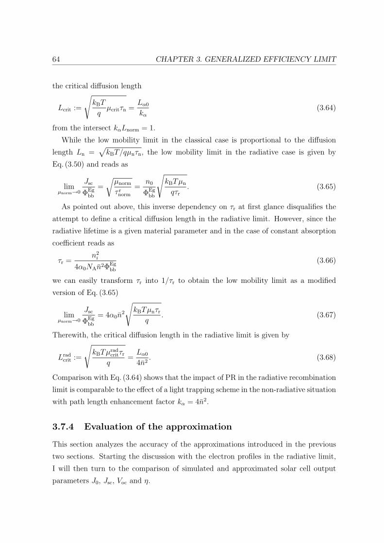
64 CHAPTER 3. GENERALIZED EFFICIENCY LIMIT
the critical diffusion length
Lcrit :=
√kBT
qµcritτn =
Lα0
kα
(3.64)
from the intersect kαLnorm = 1.
While the low mobility limit in the classical case is proportional to the diffusion
length Ln =√
kBT/qµnτn, the low mobility limit in the radiative case is given by
Eq. (3.50) and reads as
limµnorm→0
Jsc
ΦEgbb
=
õnorm
τ rnorm
=n0
ΦEgbb
√kBTµn
qτr
. (3.65)
As pointed out above, this inverse dependency on τr at first glance disqualifies the
attempt to define a critical diffusion length in the radiative limit. However, since the
radiative lifetime is a given material parameter and in the case of constant absorption
coefficient reads as
τr =n2
i
4α0NAn2ΦEgbb
(3.66)
we can easily transform τr into 1/τr to obtain the low mobility limit as a modified
version of Eq. (3.65)
limµnorm→0
Jsc
ΦEgbb
= 4α0n2
√kBTµnτr
q. (3.67)
Therewith, the critical diffusion length in the radiative limit is given by
Lradcrit :=
√kBTµrad
critτr
q=
Lα0
4n2. (3.68)
Comparison with Eq. (3.64) shows that the impact of PR in the radiative recombination
limit is comparable to the effect of a light trapping scheme in the non-radiative situation
with path length enhancement factor kα = 4n2.
3.7.4 Evaluation of the approximation
This section analyzes the accuracy of the approximations introduced in the previous
two sections. Starting the discussion with the electron profiles in the radiative limit,
I will then turn to the comparison of simulated and approximated solar cell output
parameters J0, Jsc, Voc and η.
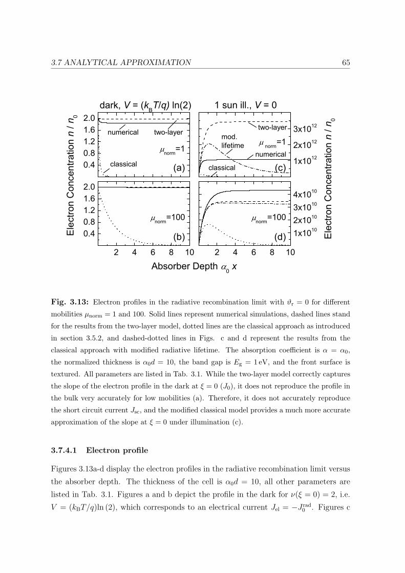
3.7 ANALYTICAL APPROXIMATION 65
0.40.81.21.62.0
classical
numerical
norm=1
Ele
ctro
n C
once
ntra
tion n
/ n0
norm=100
(a)
two-layer
1x10¹²
2x10¹²
3x10¹²
mod.lifetime
norm=1
dark, V = (kBT/q) ln(2) 1 sun ill., V = 0
(c)
two-layer
numerical
classical
2 4 6 8 10
0.40.81.21.62.0
(b)2 4 6 8 10
1x10¹⁰
2x10103x1010
4x10¹⁰
norm=100
Absorber Depth 0 x
Ele
ctro
n C
once
ntra
tion n
/ n0
(d)
Fig. 3.13: Electron profiles in the radiative recombination limit with ϑr = 0 for different
mobilities µnorm = 1 and 100. Solid lines represent numerical simulations, dashed lines stand
for the results from the two-layer model, dotted lines are the classical approach as introduced
in section 3.5.2, and dashed-dotted lines in Figs. c and d represent the results from the
classical approach with modified radiative lifetime. The absorption coefficient is α = α0,
the normalized thickness is α0d = 10, the band gap is Eg = 1 eV, and the front surface is
textured. All parameters are listed in Tab. 3.1. While the two-layer model correctly captures
the slope of the electron profile in the dark at ξ = 0 (J0), it does not reproduce the profile in
the bulk very accurately for low mobilities (a). Therefore, it does not accurately reproduce
the short circuit current Jsc, and the modified classical model provides a much more accurate
approximation of the slope at ξ = 0 under illumination (c).
3.7.4.1 Electron profile
Figures 3.13a-d display the electron profiles in the radiative recombination limit versus
the absorber depth. The thickness of the cell is α0d = 10, all other parameters are
listed in Tab. 3.1. Figures a and b depict the profile in the dark for ν(ξ = 0) = 2, i.e.
V = (kBT/q)ln (2), which corresponds to an electrical current Jel = −J rad0 . Figures c

66 CHAPTER 3. GENERALIZED EFFICIENCY LIMIT
and d depict the profile under illumination and short circuit conditions with ν(ξ = 0) =
1, which yields the short circuit current Jsc. Both cases are displayed for a normalized
mobility µnorm = 1 (a and c) and µnorm = 100 (b and d).
In all figures, solid lines represent the results from the numerical simulations, dashed
lines are the profiles from the two-layer model, and in the illuminated case, dashed-
dotted lines stand for the profile computed with the modified radiative lifetime. For
comparison, the profiles computed with the classical approach are displayed as well
(dotted lines). These results are obtained numerically by simply leaving out the internal
generation term in Eq. (3.3) as described in section 3.4.2.
Let us first discuss the dark profiles in Fig. 3.13 with µnorm = 1. The short diffusion
length leads to a steep exponential decay towards δν = 0 in the classical profile. In
contrast, photon recycling leads to an increased electron density which is constant
almost throughout the absorber depth.
This feature is correctly captured by the two-layer model. However, the exact level
of the electron density is not necessarily reproduced accurately. Without external
irradiation, i.e. G = H = 0, it follows E = 0 from Eq. (C.26). Therefore, the electron
profile from Eq. (C.8) with Lnrnorm →∞ is constant
δν2 = F = −tanh
(ξpr
Lnorm
)sinh
(ξpr
Lnorm
)+ cosh
(ξpr
Lnorm
)(3.69)
for ξ ≥ ξpr. For a thick cell with absorptance a = 1 it holds ξpr = τ rnorm = 0.028 which
yields ν2 = 1.99 for µnorm = 1. As can be seen in Fig. 3.13a, this level is higher than
the level of ν2 = 1.84 obtained from the numerical simulations. The two-layer model
is only capable of reproducing the complete profile in the high mobility limit depicted
in Fig. 3.13b.
However, for the saturation current, only the initial slope dν/dξ at ξ = 0 is of inter-
est. In the low mobility limit, the numerical approach with PR, the two-layer model,
and the classical approach without PR result in the same dependence√
µnormτ rnorm.
And since the thickness ξpr has been chosen appropriately the radiative recombination
current J rad0 = a in the high mobility limit is rendered correctly by definition of the
model. This means that in both limits, the initial slope dν/dξ at ξ = 0 is reproduced
correctly by the two-layer model. Abberations can occur only in the intermediate
mobility range.
Whereas the saturation current J0 depends only on the slope at ξ = 0, the short

3.7 ANALYTICAL APPROXIMATION 67
circuit current is related to the integral of the electron profile in the dark. The proba-
bility that an electron generated at a position ξ contributes to the short circuit current
is given by the collection efficiency fC(ξ). Then, the total short circuit current reads
as
Jsc =
∫ α0d
0
Gsun(ξ)fC(ξ)dξ. (3.70)
From a reciprocity relation derived by Donolato [67] the collection efficiency is linked
to the electron profile in the dark according to
fC(ξ) =δν(ξ)
exp(
qVkBT
)− 1
. (3.71)
Therefore, the short circuit current is related to the spatial integral over the electron
profile in the dark. From the inaccuracy of the electron profile it is thus clear that
the two-layer model does not reproduce the short circuit current correctly for low
mobilities.
Let us now turn to the profiles under illumination. Here, only the initial slope at
ξ = 0 is important for the computation of the short circuit current. Figures 3.13c and
d illustrate again the difference between the correct profile with photon recycling (solid
lines) and the profile obtained with the classical treatment (dotted lines). As has been
discussed in section 3.5.2, the PR prevents a decrease of the profile towards the back
contact in the radiative limit. Again, this feature is correctly captured by the two-layer
model. But again, a different level deep in the bulk is predicted.
In contrast to the two-layer model, the modified classical model with the increased
radiative lifetime τ r,modnorm from Eq. (3.62) does not reproduce the qualitative features of
the correct profile with photon recycling. The profile of the modified classical approach
(dashed-dotted lines) decreases towards the back contact as does the profile from the
classical approach (dotted lines). However, the modified classical approach is designed
in such a way that the low mobility limit for the short circuit current is identical to
the theoretical limit 2n√
µnorm. Therefore, the slope of the electron profile at ξ = 0 in
Fig. 3.13c is almost identical to the slope obtained from the numerical simulation.
As pointed out at the beginning of this section, a consistent quasi-classical analytical
model that is able to reproduce both, J rad0 and Jsc correctly, does not exist because
of the inherent discrepancy with respect to the low mobility limits of J rad0 and Jsc (cf.

68 CHAPTER 3. GENERALIZED EFFICIENCY LIMIT
p. 58). Therefore, I use the two-layer model to compute J0 and the modified-lifetime
model to compute Jsc. The combination of the two models thus yields a fairly accurate
approximation of the numerical results which allows us to analytically calculate the
efficiency of pn-junction solar cells in the whole thickness, mobility and lifetime range.
The results of these computations are presented in the next section.
3.7.4.2 Photovoltaic output parameters
Figures 3.14a-d and 3.15a-d demonstrate the accuracy of the analytical approximations
for a solar cell with textured front surface, a constant absorption coefficient α = α0
and a cell thickness α0d = 0.1 and 10. All other parameters are listed in Tab. 3.1.
The figures display the normalized saturation current J0/ΦEgbb (a), the normalized
short circuit current Jsc/JSQsc (b), the open circuit voltage Voc (c), and the efficiency
η (d) versus the normalized mobility µnorm for different ratios ϑr = 10−2, 1 and 100
of radiative and non-radiative lifetime. Open squares represent the numerical results,
solid lines are the approximated results where both, J0 and Jsc are computed with the
two-layer model, and dashed lines stand for the results obtained from combining the
saturation current J0 from the two-layer model with the short circuit current Jsc from
the modified-lifetime model. Note in Fig. 3.15 that at low mobilities the numerical
results are prone to be flawed with discretization errors when the diffusion length is
smaller than the discretization interval d/N (see p. 173 in appendix B.7).
The two-layer model is well suited to describe the saturation current in the com-
plete lifetime and mobility range. The model is constructed in such a way that in
the radiative recombination limit the high mobility limit of J0 converges towards the
absorptance of the sample. The low mobility converges towards√
µnorm/τ rnorm and
therewith also meets the requirements. Only in an intermediate range around the
critical mobility µnormcrit does the approximation differ from the numerical results. The
difference is more pronounced in solar cells with a thickness larger than the absorption
length (Fig. 3.15a), where PR is more important than in solar cells with a thickness
α0d < 1 (Fig. 3.14a).
The two-layer model also yields a correct approximation of the short circuit current
for ϑr > 1 as depicted in Fig. 3.14b and Fig. 3.15b (solid lines). The differences to the
numerical results (squares) stem from the errors in the approximation of the generation
profile, since the profile of a cell with textured surface can not completely be reproduced

3.7 ANALYTICAL APPROXIMATION 69
100
(c)1
10-2
J0 / JS
Q0
(b)
600
700
8000d = 0.1
VO
C [m
V]r / nr =
100
(a)
100
1
10-2
10-2 100
0.20.40.60.81.0
JS
C / JS
QS
C
10-2
1100
10-2 100
10
20
30(d)
Normalized Mobility norm
[%
]
100
1
10-2
Fig. 3.14: Photovoltaic output parameters versus the normalized mobility µnorm. The
absorption coefficient is α = α0, the normalized thickness is α0d = 0.1, the band gap is
Eg = 1 eV, and the front surface is textured. All parameters are listed in Tab. 3.1. Open
squares are the numerical results, solid lines are the results from the two-layer model, and
dashed lines are the results from combining the saturation current from the two-layer model
with the short circuit current from the modified-lifetime model. While the two-layer model
provides a good approximation of the saturation current, it is not suited to describe the
short circuit current accurately. In combination with the modified-lifetime model however, it
presents a fairly accurate analytical model to compute the efficiency of pn-junction solar cells
in the whole lifetime and mobility range. (Note that the modified-lifetime model (dashed
lines) is only included in figures b-d.)
by two exponential functions.
However, the approximation of Jsc in the radiative recombination limit with ϑr → 0
is rather crude. In particular, the low mobility limit for the short circuit current is
given by the radiative diffusion length Lnorm =√
µnormτ rnorm (corrected by the optical

70 CHAPTER 3. GENERALIZED EFFICIENCY LIMIT
100
102
10-4
(c)
1
J0 / JS
Q0
(b)
600
700
80010-4
VO
C [m
V]r / nr =
100
(a)
100
1
10-2 100
0.20.40.60.81.0
10-4
JS
C / JS
QS
C
1100
0d = 10
10-2 100
10
20
3010-4(d)
Normalized Mobility norm
[%
]
1001
Fig. 3.15: Photovoltaic output parameters versus the normalized mobility µnorm. The
absorption coefficient is α = α0, the normalized thickness is α0d = 10, the band gap is
Eg = 1 eV, and the front surface is textured. All parameters except for the thickness are
identical to the parameters in Fig. 3.14. Open squares are the numerical results, solid lines
are the results from the two-layer model, and dashed lines are the results from combining the
saturation current from the two-layer model with the short circuit current from the modified-
lifetime model. For low mobilities, discretization errors lead to flawed numerical results,
which are therefore not displayed here.
term in Eq. (3.61)). It is therewith by roughly a factor of 4n2 smaller than the limit√µnorm/τ r
norm.
The modified-lifetime model is not based on physical reasons but it is constructed
to reproduce the radiative low mobility limit of the short circuit current correctly. As
Fig. 3.14b and Fig. 3.15b demonstrate (dashed lines), the model yields a surprisingly
accurate approximation of the numerical results. Only in an intermediate range around
the critical mobility does the approximation depart from the numerical results.

3.8 ENERGY-DEPENDENT ABSORPTION COEFFICIENT 71
In the next step we combine the saturation current from the two-layer model with the
short circuit current from the modified-lifetime model to obtain the open circuit voltage
and the efficiency (dashed lines). For comparison, the results where both currents are
taken from the two-layer model are displayed as well (solid lines). For low mobilities
the underestimated short circuit current leads here to a large error in the open circuit
voltage which for all lifetime ratios ϑr < 1 converges towards the voltage corresponding
to ϑr = 1.
The combined model provides a simple tool to compute the efficiency of pn-junction
solar cells for all thicknesses and different kinds of front surfaces. It is capable of
predicting the efficiency with an error of typically less than 0.5 % (absolute). The error
is largest for the radiative recombination limit in the mobility range approximately two
decades below the critical mobility µnormcrit . In this range, the error can be es large as
3.5 % (absolute).
The model replaces the exact but very complicated numerical model with a simple
analytical approach. It is here only presented for the case with constant absorption
coefficient but can be extended to energy-dependent absorption coefficients (see section
3.9.1.
3.8 Energy-dependent absorption coefficient
So far, all simulations have been performed for the hypothetical case with constant ab-
sorption coefficient. This section analyzes the influence of energy-dependent absorption
coefficient α(E). With respect to the spectral dependence of α(E) on the photon energy
E I distinguish the three different cases listed in Tab. 3.2: (i) The hypothetical case of
constant absorption above the band gap energy, (ii) direct semiconductors where the
absorption of photons occurs via direct transitions without a change in momentum and
which therefore exhibit a square-root dependence of the absorption coefficient on the
energy [68, p. 36], and (iii) indirect semiconductors, where phonons are needed for mo-
mentum conservation during light absorption and which therefore exhibit a parabolic
dependence [68, p. 38].
The parameter α0 in Tab. 3.2 is the absorption coefficient at the photon energy
E = Eg + kBT for all three cases. Note that the choice of Eg + kBT as this crossover
energy is somewhat arbitrary. To compare the three cases, we assume identical α0

72 CHAPTER 3. GENERALIZED EFFICIENCY LIMIT
Tab. 3.2: Spectral dependence of the absorption coefficient.At E = Eg + kBT , all types
feature the absorption coefficient α(Eg + kBT ) = α0.
Type α(E)
constant α0
direct α0
√E−Eg
kBT
indirect α0
(E−Eg
kBT
)2
for all. In reality, though, indirect semiconductors possess much lower absorption
coefficients than direct semiconductors, which leads to a crossover energy more in
the proximity of Eg + 1 eV. However, such an approach would imply that for a given
sample thickness d the average absorptance in an indirect semiconductor would be much
smaller than in a direct semiconductor, which in turn would distort the comparability
of the currents. Therefore, I chose to stick with the crossover energy Eg + kBT close
to the band gap energy.
Figures 3.16a-i demonstrate the influence of the spectral dependence of the absorp-
tion coefficient on the currents Jsc and J0, the open circuit voltage Voc, and the efficiency
η. All quantities are again normalized to their respective maximum values in the SQ
limit. In analogy to the representation in Fig. 3.4, all quantities are displayed vs. the
thickness α0d of the solar cell. The front surface is textured.
Constant absorption The energy independent light absorption leads to identical
generation profiles for solar and black body irradiation. Therefore, the external quan-
tum efficiency EQE(E) is independent of the photon energy, and Rau’s reciprocity
relation [16] which relates the EQE to the radiative recombination current as eluci-
dated in section 3.7 on page 58, holds not only for the spectral quantity EQE(E) but
also for the integrated spectrum. In consequence, the normalized currents Jsc/JSQsc and
J0/JSQ0 are identical (Fig. 3.16a). As in Fig. 3.4a, the currents approach the absorp-
tance a of the sample for sufficiently large mobilities. For lower mobilities, however,
the currents are limited by insufficient transport.
Since the ratios Jsc/JSQsc and J0/J
SQ0 are independent of the absorber thickness,
it always holds Jsc/J0 = JSQsc /JSQ
0 and, therefore, the open circuit voltage is always
Voc = V SQoc (Fig. 3.16d). Accordingly, the efficiency is exclusively determined by the

3.8 ENERGY-DEPENDENT ABSORPTION COEFFICIENT 73
0.20.40.60.81.0 norm
= 100
0.011
J /
J SQ
JSC J0
(d)
(a)
0.20.40.60.81.0
(g)
J0
JSC
1.00
1.05
1.10 (b)
VO
C /
VS
QO
C
norm
(e)
1.00
1.05
1.10
indirectdirect
(h)
norm
constant
10-3 10-2 10-1
0.20.40.60.81.0 (c)
/ S
Q
Norm. Thickness 0d 10-3 10-2 10-1
(f)
10-3 10-2 10-1
0.20.40.60.81.0(i)
Fig. 3.16: Currents Jsc and J0 in the radiative recombination limit with ϑr = 0 normalized
to the maximum values in the Shockley-Queisser limit vs cell thickness d for a textured front
surface (a, d, g). The band gap is Eg = 1 eV and the front surface is textured. I distinguish
between constant absorption above the band gap (a-c), a direct semiconductor (d-f), and
an ındirect semiconductor (g-i). The spectral dependence of the absorption coefficient α(E)
in comparison to the spectrum of the incident light leads to different spatial generation
profiles for solar and black body irradiation and, therefore, to differences between Jsc and
J0. Figures b, e, and h display the resulting normalized open circuit voltage Voc/V SQoc . With
the normalized short circuit current being larger than the normalized saturation current for
small thicknesses, the open circuit voltage exceeds the SQ limit V SQoc (e, h). The efficiency
η/ηSQ displayed in Figs. c, f, and i is mainly dominated by the short circuit current. Apart
from the absorption coefficient, all parameters are listed in Tab. 3.1.
74 CHAPTER 3. GENERALIZED EFFICIENCY LIMIT
loss in the short circuit current (Fig. 3.16b).
Direct absorption Due to the spectral dependence of the absorption coefficient,
the solar spectrum and the 300 K black body spectrum cause different generation pro-
files. Consequently, the absorptance a(E, d) is energy-dependent, and the average
absorptance as defined in appendix B.7 is different for the two spectra. Therefore, the
reciprocity relation is restricted to the spectral quantities, and Jsc/JSQsc is not identical
to Jo/JSQ0 anymore.
Since the spectral density of the solar spectrum is larger for higher photon energies
when compared to the density of the black body spectrum, the average absorption
coefficient is also larger for the solar spectrum. This means that for small absorber
thicknesses the average absorptance asun of the solar spectrum exceeds the average
absorptance abb of the black body spectrum, and, therefore, Jsc/JSQsc in Fig. 3.16d is
larger than J0/JSQ0 .
Consequently - and at first glance astonishingly - the open circuit voltage Voc in
Fig. 3.16e exceeds the open circuit voltage V SQoc for low thicknesses. The efficiency in
Fig. 3.16f, however, does not exceed the SQ efficiency ηSQ because with decreasing thick-
ness the absorption losses that result in a reduction of Jsc more than counterbalance
the increase in Voc.
The detailed discussion in section 3.8.1 reveals that such efficiency enhancement
above the SQ limit is indeed possible, but only for small band gap energies. Effectively,
the variation of the spectral dependence of the absorption coefficient can be regarded
as an increase of the band gap energy. In particular, the indirect semiconductor with
the parabolic dependence of α exhibits hardly any absorption below Eg + kBT when
the sample is thin enough.
Indirect absorption The reasoning given for the direct semiconductor holds for
indirect semiconductors as well. The difference between Jsc and J0 in Fig. 3.16g is
even more pronounced. For energies E < Eg + kBT the absorption coefficient is much
smaller than α0 which implies a reduced abb. For E > Eg + kBT on the other hand, α
is much larger than α0 which results in an amplified asun. Note again that the choice
of Eg + kBT as a crossover point is somewhat arbitrary and does not reflect crossover
points of real semiconductor materials.

3.8 ENERGY-DEPENDENT ABSORPTION COEFFICIENT 75
Note that with respect to the shift of the critical thickness towards smaller thick-
nesses, the opposite holds true for the saturation current J0 because the black body
spectrum possesses its maximum at an energy much below the band gap Eg = 1 eV
and only the exponentially decreasing Boltzmann tail of the spectrum is relevant for
the saturation current. Therefore, the relevant energy regime for J0 lies between Eg
and Eg +kBT , where direct and indirect semiconductors have an absorption coefficient
below α0.
3.8.1 Thickness-dependent current enhancement
Figure 3.16d shows that for a certain cell thickness d the short circuit current Jsc
features a maximum. This section takes a closer look at this phenomenon and explains
the underlying mechanism. As will be discussed in the following, this mechanism
involves the relationship between photon absorption and emission and carrier collection.
In principle, there are two questions arising from the observations in Fig. 3.16d that
need to be answered: (i) Why does the short circuit current only feature a maximum
for low mobilities and (ii) Why does this maximum not occur for energy-independent
absorption coefficient?
3.8.1.1 High mobility
Let us first consider the high mobility limit of the short circuit current, which is given
by the absorptance. In this context, high mobility limit means that the minority
carrier diffusion length is larger than the average absorption length of the photon flux
impinging on the cell, i.e. that all generated carriers contribute to the short circuit
current.
As pointed out in section 3.6.1, the absorptance increases monotonically with in-
creasing sample thickness. Even though the generation rate close to the front surface
decreases with increasing thickness when the influence of multiple reflections recedes,
the overall absorptance given by the integrated generation rate over the cell thickness
always increases with increasing thickness. Consequently, for high mobilities the short
circuit current increases monotonically with increasing thickness as well and does not
show a maximum over the cell thickness.

76 CHAPTER 3. GENERALIZED EFFICIENCY LIMIT
3.8.1.2 Low mobility
The case is different for lower mobilities. If the collection length (i.e. the diffusion
length) of the photo-generated carriers is smaller than the absorption length then not
all generated carriers can contribute to the short circuit current. Carriers that are
generated deep in the bulk are not collected and thus recombine.
In the radiative recombination limit, a carrier that is absorbed but not collected can
only be emitted by the cell. We thus have to consider the relation between absorption
and emission length. To do so, we have to differentiate between energy-independent
and energy-dependent absorption coefficient.
Constant absorption coefficient In the case of constant absorption coefficient as
depicted in Fig. 3.16a, the emission length is identical to the absorption length. Let
us now consider the influence of the cell thickness on the carrier collection in the low
mobility limit. As long as the thickness is smaller than the diffusion length, all gener-
ated carriers are collected and the short circuit current is identical to the absorptance.
With increasing thickness, however, not all generated carriers are collected anymore
and the current is lower than the absorptance. Once the thickness exceeds the absorp-
tion length, Jsc/JSQsc saturates. The saturation level is below unity and is determined
by the collection length, i.e. the carrier mobility.
Energy-dependent absorption coefficient Let us now turn to energy-dependent
light absorption. Consider the low mobility limit of the short circuit current as depicted
in Fig. 3.16d. In the following, I will illustrate, why the current features a maximum
over the sample thickness.
As long as the thickness is smaller than the diffusion length, the short circuit
current is again equal to the absorptance. It keeps increasing with a lower slope
than the absorptance until the thickness is identical to the average absorption length
Lα,norm = α0/(5α0) = 0.2 (cf. Tab. B.2 on page 172) for the solar irradiation. Any
further increase of the thickness, however, leads to increased emission of internally
reabsorbed carriers, while the absorptance of solar radiation essentially remains unaf-
fected. Therefore, the current decreases until the thickness is equal to the emission
length Lem,norm = α0/α0 = 1, which is identical to the absorption length of the black
body spectrum. For thicknesses larger than the emission length, the current saturates
3.8 ENERGY-DEPENDENT ABSORPTION COEFFICIENT 77
at a slightly higher level than in Fig. 3.16a because of the higher average absorption
coefficient for the solar irradiation.
Summing up, the discrepancy between absorption and emission length leads to the
maximum of the short circuit current over the cell thickness. In a range Lα,norm <
α0d < Lem,norm any increase of the thickness leads to emission losses which are larger
than the gain in absorptance and therefore to a decreasing current. Since for the black
body spectrum the absorption length is equal to the emission length, this effect can
not be seen in the saturation current, which therefore increases monotonically with the
cell thickness.
3.8.2 Thickness-dependent efficiency enhancement
In the last section we have seen that the discrepancy between the absorptance of solar
and black body irradiation leads to a maximum in the short circuit current for low
mobilities. This discrepancy, which in a certain thickness range leads to Jsc(d)/JSQsc >
J0(d)/JSQ0 for all mobilities, is also responsible for the enhancement of the open circuit
voltage Voc(d) above V SQoc as depicted in Fig. 3.16e and h.
From a thermodynamic point of view, the reduced radiative recombination current
in comparison to the short circuit current can leads to a reduced entropy production
per absorbed photon [69], which results in higher open circuit voltages. Unfortunately,
the voltage enhancement occurs in a thickness range, where the cell is so thin that the
short circuit current Jsc/JSQsc is significantly lower than unity. Therefore, the efficiency
as the product of Jsc and Voc does not exceed the Shockley-Queisser limit.
This situation changes, when the band gap energy of the solar cell is reduced. Figure
3.17 demonstrates that for a cell with Eg = 0.5 eV, the maximum radiative efficiency,
i.e. the high mobility limit with µnorm = 104, can indeed exceed the SQ limit for
this particular band gap. The figure depicts the normalized efficiency versus the cell
thickness for a semiconductor with constant absorption coefficient (const), a direct
semiconductor (dir), and an indirect semiconductor (ind). Both, the direct and the
indirect semiconductor feature a thickness regime, where the normalized efficiency is
larger than unity. Especially the absorptance spectrum of the indirect semiconductor
as depicted in Fig. 3.17 leads to the efficiency enhancement of almost 15 % (relative) for
a thin cell with thickness α0d ≈ 3× 10⁻⁴. These considerations have also been carried
out in a similar form by Araujo and Martı [70]. They have shown that even with the

78 CHAPTER 3. GENERALIZED EFFICIENCY LIMIT
10-3 10-2 10-1 100 101
0.850.900.951.001.051.101.151.20
N
orm
. Effi
cien
cy
/ S
Q
Norm. Thickness 0d
Eg = 0.5 eV
norm = 104
const.dir.
ind.
Fig. 3.17: Normalized radiative efficiency versus cell thickness α0d for a semiconductor with
constant absorption above the band gap energy (const), a direct semiconductor (dir), and an
indirect semiconductor (ind). The band gap is Eg = 0.5 eV, the mobility is µnorm = 104, and
the front surface is textured. All other parameters are listed in Tab. 3.1. Due to the higher
absorptance of the solar irradiation compared to the black body irradiation, the efficiency
η(Eg) exceeds the SQ efficiency ηSQ(Eg) for the direct semiconductor and even more so for
the indirect semiconductor.
band gap of silicon, a maximum radiative efficiency is obtained for the (rather large)
optimal thickness d ≈ 1 mm.
The reason for this rather astonishing phenomenon lies in the fact that the energy-
dependent absorption coefficient of the solar cell translates into an energy-dependent
absorptance if the sample is thin enough. When the sample is thick enough, the ab-
sorptance is unity for all energies larger than Eg. This means that the absorptance can
be expressed by a step function as described in Eq. (2.5). Reducing the cell thickness
results in a reduction of the absorptance at energies, where the absorption coefficient
is low, i.e. at energies close to the band gap energy. This means that the absorp-

3.8 ENERGY-DEPENDENT ABSORPTION COEFFICIENT 79
tance for thin cells can again be approximated with a step function, but one that is
shifted towards higher energies. Consequently, the thickness reduction can effectively
be described as an increase of the band gap Eg. This increase of the band gap in turn
implies a higher maximum efficiency ηSQ(Eg) if the band gap is below the band gap
Eg ≈ 1.1 eV that corresponds to the global maximum efficiency ηSQ ≈ 33 %. For band
gaps larger Eg = 1.4 eV, which corresponds to the second global maximum, there is
no such efficiency enhancement for thin cells. This is because increasing the effective
band gap would only result in lower efficiencies (cmp. Fig. 3.2).
3.8.3 Maximum open circuit voltage
The previous section 3.8.2 has shown that it is possible to exceed the SQ efficiency
limit of a solar cell with given band gap if the band gap is small enough. Due to
energy-dependent light absorption, the thickness of the cell can be tuned in such a way
that almost the entire solar irradiation above the band gap is absorbed while the black
body irradiation, which occurs predominately at lower photon energies, is only partly
absorbed. Therewith, the open circuit voltage is increased above its SQ limit. If this
increase is not compensated entirely by the loss in Jsc due to incomplete absorption,
the efficiency is also increased above its SQ limit ηSQ(Eg).
This result brings up two questions: (i) What is the maximum open circuit voltage
for a given band gap energy and (ii) Is it possible to exceed even the global maximum
ηSQ ≈ 33 %, or in other words: Is there an optimal absorptance spectrum that is
superior to the step function absorptance assumed by Shockley and Queisser?
The latter question has already been answered in section A.2, which proves that
the global SQ limit of 33 %, which is obtained with a step-like absorptance function,
is indeed the ultimate maximum efficiency that can be obtained with a single junction
solar cell. A similar proof has also been derived by Araujo and Martı Ref. [70]. This
section discusses the first question of the maximum open circuit voltage obtainable
with a single junction solar cell with a given band gap energy.
It is often assumed that the maximum open circuit voltage in the SQ limit is given
by the band gap energy Eg. Indeed, Shockley and Queisser introduced a so-called
ultimate efficiency in their publication [10] that is obtained when Voc = Eg is assumed.
However, the detailed balance limit itself does not include an inherent restriction to the
open circuit voltage. The open circuit voltage is exclusively determined by the ratio of

80 CHAPTER 3. GENERALIZED EFFICIENCY LIMIT
short circuit current and saturation current, i.e. by Voc = (kBT/q)ln (Jsc/J0 + 1). The
currents in turn are entirely determined by the solar and the black body spectrum and
the absorptance a(E).
In a strict sense, it is a mere coincidence that V SQoc (Eg) is smaller than the band gap.
In fact, the SQ theory would predict Voc > Eg for highly concentrated sunlight with
concentration factors exceeding 30000.
However, the SQ theory only accounts for the spontaneous radiative recombination
of electron and holes. If the voltage exceeds the band gap, then the quasi Fermi levels
will be located in the conduction and valence band, which would result in stimulated
emission. Due to this additional recombination the maximum open circuit voltage of
a single pn-junction solar cell is indeed given by the band gap energy Eg.
3.9 Maximum efficiencies of real materials
So far, most of the discussions have focused on the hypothetical case of constant absorp-
tion coefficient to facilitate the understanding of the fundamental mechanisms involved
and to allow for relatively simple analytical expressions. As helpful as these analyses
proved for the theoretical construction of the model features, they fail to provide any
practical information.
This section analyzes the critical mobility and the efficiency limits for the three
semiconducting materials crystalline silicon (c-Si), hydrogenated amorphous silicon
(a-Si:H), and Cu(In1−x,Gax)Se2 with x = 0.26 (CIGS). Admittedly though, it needs
to be mentioned that the simulations conducted here only describe the efficiencies of
idealized pn-junction solar cells without, for instance, optical losses or recombination
in the space charge region, in the emitter or at the back contact. On the other hand,
carrier generation and collection in the space charge region are neglected as well. While
the model quite reasonably describes crystalline silicon solar cells, it is hardly suited
to simulate actual devices made of amorphous silicon or CIGS.
The parameters used for the simulations are listed in Tab. 3.3. The cell thicknesses
are chosen as typical values but also large enough to guarantee virtually complete
absorption of the solar spectrum. All solar cells are assumed to be pn-junction solar cells
with a zero reflectance textured front surface, and no recombination at the back contact.
The absorption coefficients are taken from Ref. [12] in the case of crystalline silicon

3.9 MAXIMUM EFFICIENCIES OF REAL MATERIALS 81
Tab. 3.3: Parameters used for the computation of the critical mobility of crystalline silicon
(c-Si), hydrogenated amorphous silicon (a-Si:H), and Cu(In1−x,Gax)Se2 (CIGS, x = 0.26).
Eg n α0 (Type) ni d Ref.
[ eV] [ cm−1] [ cm−3] [ µm]
c-Si 1.124 3.6 3.3 (indirect) 1.04× 10¹⁰ 200 [12,17]
a-Si:H 1.75 4 180 (indirect) 1× 10⁶ 1 [5, 71]
CIGS 1.17 3.1 11000 (direct) 3× 10⁸ 2 [72]
or from measured data and are displayed in Fig. 3.18. Table 3.3 lists the absorption
coefficients at an energy Eg+kBT and the type of the semiconductor. In contrast to the
theoretical types listed in Tab. 3.2, the measured data also include sub band gap tail-
like absorption and at higher energies abberations of the strict theoretical square-root
or parabolic dependencies on the energy.
Figures 3.19a-d, 3.20a-d, and 3.21a-d display the results of the simulations, i.e., the
saturation current J0 (a), the short circuit current Jsc (b), the open circuit voltage Voc
(c), and the efficiency η (d), versus the non-radiative lifetime τnr for different mobilities
(open symbols). The chosen mobilities vary between the materials and are chosen in
such a way that measured values fall in the displayed range. The mobilities are µn = 24,
240, and 2400 cm2( Vs)−1 for c-Si, µn = 0.34, 3.4, and 34 cm2( Vs)−1 for a-Si:H, and
µn = 0.15, 1.5, and 150 cm2( Vs)−1 for CIGS.7
For the transformation of the normalized mobility µnorm and the normalized lifetimes
τ rnorm and τnr
norm into the unit-bearing quantities µn, τr, and τnr, one requires the doping
concentration NA. I assume NA = 5×1016 cm−3 which is a typical value for silicon solar
cells. However, as section 3.10 shows, the doping concentration must not be chosen
too low in order not to violate the low-level injection assumptions, in particular in the
radiative recombination limit.
Section 3.9.3 discusses the results of the simulation. Before doing so, however, the
next section applies the analytical model of section 3.7 to the analyzed materials.
7The unconventional values result from the de-normalization of the normalized mobilities. Note
that for CIGS, the chosen range is by a factor of 10 larger than for the other two cases because of the
uncertainty connected with measured values.

82 CHAPTER 3. GENERALIZED EFFICIENCY LIMIT
1.5 2.0 2.5
102
103
104
105
c-Si
a-Si:H
A
bsor
ptio
n C
oeffi
cien
t [c
m-1]
Energy E [eV]
CIGS
Fig. 3.18: Experimental absorption coefficients of crystalline silicon (c-Si, squares), hydro-
genated amorphous silicon (a-Si:H, circles), and Cu(In1−x,Gax)Se2 (CIGS, triangles) with
x = 0.26 versus the photon energy. The measured data are fit with either a square-root
function for the direct semiconductor CIGS or a parabolic function in the case of crystalline
and amorphous silicon (lines). Table 3.3 lists the fit parameters. Amorphous silicon exhibits
a significant sub band gap absorption in band tail states. In the chosen spectrum of CIGS
the band tails are much less pronounced. In crystalline silicon and CIGS, the absorption
coefficient shows a sharp increase at photon energies above 2 eV that cannot be explained
with the simple parabolic or square-root dependence.
3.9.1 Analytical approximation
This section discusses the applicability of the analytical model derived in section 3.7
to the three materials under investigation and introduces necessary modifications. The
model with constant absorption in section 3.7 was based on the analysis of the low
mobility limits of saturation and short circuit current. Hence, the main question that
needs to be answered is, what influence the energy-dependent absorption coefficient
has on those low-mobility limits.

3.9 MAXIMUM EFFICIENCIES OF REAL MATERIALS 83
10-16
10-14
10-12
J0 [A
/cm
2 ]
(a)
(b)
(c)
(d)
240
n =
24 cm2(Vs)-1
2400
0.7
0.8
VO
C [V
]
24024
2400
10-5 10-3 10-1
25303540
c-Si, d = 200 m, NA = 5x1016 cm-3
2400
JS
C [m
A/c
m2 ]
24
240
10-5 10-3 10-1
20
30
Non-radiative Lifetime nr [s]
[%
]
24240
2400
Fig. 3.19: Simulation results of a crystalline silicon pn-junction solar cell (open symbols):
Saturation current J0 (a), short circuit current Jsc (b), open circuit voltage Voc (c), and
efficiency η (d) versus the non-radiative lifetime τnr. The thickness of the solar cell is d =
200µm and the doping density is NA = 5 × 1016 cm−3. The minority carrier mobility is
assumed as µn = 24, 240, and 2400 cm2(Vs)−1.
3.9.1.1 Saturation current
The low mobility limit of J rad0 can still be obtained in the simple fashion of section
3.6.2, where the generation rates need to be augmented by integrating over the photon
energy. Interestingly, the relation limµnorm→∞ J rad0 /ΦEg
bb =√
µnorm/τ rnorm is only valid for
the integrated spectrum, but not for the spectral radiative saturation current jrad0 (E)
that is obtained under monochromatic excitation with the black body intensity φbb(E).
This is because even with monochromatic generation rate gbb(E), the internal gener-
ation still includes the complete integral Gint =∫∞0
gint(E)dE. The thermodynamic
equilibrium as expressed in Eq. (3.46) requires illumination with the integrated black

84 CHAPTER 3. GENERALIZED EFFICIENCY LIMIT
10-24
10-22
10-20
n =
0.34 cm2(Vs)-1
J0 [A
/cm
2 ]
(a) (c)
(b) (d)
3.4
34
1.01.11.21.3
VO
C [V
]
3.434
0.34
10-9 10-6 10-3
10
15
20
a-Si:H, d = 1 m, NA = 5x1016 cm-3
JS
C [m
A/c
m2 ]
34
0.34
3.4
10-9 10-6 10-3
10
20
30
Non-radiative Lifetime nr [s]
[%
]
3.434
0.34
Fig. 3.20: Simulation results of an amorphous silicon pn-junction solar cell (open symbols):
Saturation current J0 (a), short circuit current Jsc (b), open circuit voltage Voc (c), and
efficiency η (d) versus the non-radiative lifetime τnr. The thickness of the solar cell is d = 1µm
and the doping density is NA = 5× 1016 cm−3. The minority carrier mobility is assumed as
µn = 0.34, 3.4, and 34 cm2(Vs)−1.
body spectrum, which implies that the approximation performed in Eq. (3.47) is only
valid for the integrated spectrum.
The high mobility limit is also still given by the integrated absorbed black body
spectrum Φabsbb as listed in Tab 3.4. To define the thickness ξpr of layer 1 in the two
layer model, we need the absorptance a = Φabsbb /ΦEg
bb . Then we can apply the two-layer
model from section 3.7.2 without any other modifications.
Figures 3.19a, 3.20a, and 3.21a display the analytical saturation currents computed
with the two-layer model as solid lines. The figures demonstrate the excellent agreement
of the analytical model and the numerical simulations.

3.9 MAXIMUM EFFICIENCIES OF REAL MATERIALS 85
10-17
10-15
J0 [A
/cm
2 ]
(a) (c)
(b) (d)
150
1.5
n =
0.15 cm2(Vs)-1 0.7
0.8
0.9
VO
C [V
]
150
1.5
0.15
10-8 10-6 10-4
25
30
35
40
Cu(In,Ga)Se2, d = 2 m, NA = 5x1016 cm-3
JS
C [m
A/c
m2 ]
150
1.5
0.15
10-8 10-6 10-4
10
20
30
Non-radiative Lifetime nr [s]
[%
]
150
1.5
0.15
Fig. 3.21: Simulation results of a Cu(In,Ga)Se2 pn-junction solar cell (open symbols):
Saturation current J0 (a), short circuit current Jsc (b), open circuit voltage Voc (c), and
efficiency η (d) versus the non-radiative lifetime τnr. The thickness of the solar cell is d = 2 µm
and the doping density is NA = 5× 1016 cm−3. The minority carrier mobility is assumed as
µn = 0.15, 1.5, and 150 cm2(Vs)−1.
3.9.1.2 Short circuit current
The derivation of the modified-lifetime model for the determination of the short circuit
current in section 3.7.3 was based on the reciprocity between the short circuit current
and the radiative recombination current. This section discusses the influence of the
energy-dependent absorption coefficient on the reciprocity relation.
Let us first have a look at the relationship between short circuit current and radiative
saturation current in the radiative recombination limit if the absorption coefficient
is energy-dependent. In section 3.6.2 we have seen that the low mobility limit of
short circuit and saturation current is identical if the absorption coefficient is energy-

86 CHAPTER 3. GENERALIZED EFFICIENCY LIMIT
independent. In the following, I explain, why this relation does not hold for energy-
dependent light absorption, and what consequences this fact implies for the modified
lifetime model.
For energy-dependent light absorption, the reciprocity theorem Eq. (3.55) is still
valid, but now has to be considered separately for each individual photon energy E
according to
EQE(E) =jsc(E)
φsun(E)=
jrad0 (E)
φbb(E). (3.72)
Here, the spectral currents refer to the short circuit current jsc(E) and saturation
current j0(E) that are obtained under monochromatic illumination at the energy E
with intensity φsun(E) or φbb(E)8. The total currents Jsc and J rad0 are then obtained
by integrating the quantum efficiency EQE(E) weighted with the corresponding photon
flux φsun(E) or φbb(E) over all energies E. Therewith, we arrive at
Jsc
Φsun
=
∫∞0
EQE(E)φsun(E)dE∫∞0
φsun(E)dE6=
∫∞0
EQE(E)φbb(E)dE∫∞0
φbb(E)dE=
J rad0
Φbb
. (3.73)
Only if the EQE were energy-independent, would the reciprocity relation hold for
the integrated currents as well. For high mobilities, all photo-generated carriers are
collected and the quantum efficiency EQE(E) equals the absorptance a(E). If the
sample is sufficiently thick and subbandgap absorption is neglected, then a(E) = 1 for
energies E ≥ Eg. This case is equivalent to the monochromatic case. For the general
case with energy-dependent absorptance a(E) and/or lower mobilities, however, the
reciprocity holds only for the spectral quantities jsc(E) and j0(E). But unfortunately,
this spectral reciprocity does not help, since - as section 3.9.1.1 has shown - there is no
simple analytical expression for the low mobility limit of jrad0 (E).
In the case of low mobilities, carrier collection is limited and the quantum effi-
ciency EQE(E) is smaller than the absorptance a(E), i.e. even more energy-dependent.
Therefore, and because they are weighted with the different spectra φsun(E) and φbb(E),
the integrated short circuit current Jsc and the integrated saturation current J rad0 fea-
ture different low mobility limits.
8Note that the reciprocity relation has to consider the angular distribution of solar and black body
radiation as well. Therefore, Eq. (3.72) holds only for solar cells with a Lambertian texture that
ensures complete directional randomization of the incident light rays.

3.9 MAXIMUM EFFICIENCIES OF REAL MATERIALS 87
In sections 3.6.2 and 3.6.3, we have used the equivalence of the low mobility limit of
Jsc and J rad0 to derive an expression for the critical mobility and later for the modified
lifetime τmodnorm from Eq. (3.63). This path is now blocked. For the short circuit current,
no simple low mobility limit is available. However, an analytical approximation for Jsc
can be derived from fitting the results of the numerical simulations with help of the
modified lifetime model.
From the simulation results one finds that the low mobility limit of the short cir-
cuit current is still proportional to the square-root√
µnorm according to Jsc/Φabssun =
cµ(ϑr)√
µnorm, where the proportionality constant cµ(ϑr) depends on the ratio ϑr of
radiative and non-radiative lifetime.
Even though being aware of the crudeness of the approximation, I assume that not
only under monochromatic illumination with excitation flux φsun(E), but also under
illumination with the integrated spectrum Φsun, the short circuit current can be de-
scribed with the modified lifetime model resulting in Eq. (3.60). If the cell is thick
enough, so that virtually all photons are absorbed during the first transition through
the cell, then it holds F0 = Φabssun (see Tab. 3.4) and Fr = 0, and Eq. (3.60) simplifies to
Jsc
Φabssun
=k2
αL2norm
1− k2αL2
norm
−1 +
tanh(
α0dLnorm
)
kαLnorm
+exp (−kαα0d)
cosh(
α0dLnorm
) . (3.74)
Here, the quantity kα = klamαsun/α0 comprises the average absorption coefficient
αsun as well as the factor klam = 1 for plane front surfaces or klam = 2 for tex-
tured surfaces which accounts for the diffraction of light at the textured front surface
(with an angle of 60). As in section 3.7.3, the normalized diffusion length reads as
Lnorm =√
µnormτmodnorm, where τmod
norm is the modified lifetime. The modified lifetime is
given by 1/τmodnorm = 1/τnr
norm + 1/τ r,modnorm according to Eq. (3.63). However, τ r,mod
norm is no
longer given by Eq. (3.62) because the low mobility limit of Jsc and J0 are not identical.
Therefore, we have to extract τ r,modnorm from fitting the numerical results.
To obtain the two unknown quantities kα and τ r,modnorm , I proceed as follows: First
I fit Eq. (3.74) to the numerical data for ϑr À 1, where τmodnorm = τnr
norm, to obtain
kα. Then I extract the modified radiative lifetime τ r,modnorm . In analogy to Eq. (3.62), I
define τ r,modnorm = 1/(crτ
rnorm) and use the radiative lifetime multiplication factor cr as a
fit parameter, which I extract from fitting Eq. (3.74) to the numerical data for ϑr = 0.
Table 3.4 displays the fit parameters for crystalline silicon, amorphous silicon, and

88 CHAPTER 3. GENERALIZED EFFICIENCY LIMIT
Tab. 3.4: Parameters obtained from the numerical computation of the critical mobility
of crystalline silicon (c-Si), hydrogenated amorphous silicon (a-Si:H), and Cu(In1−x,Gax)Se2
(CIGS, x = 0.26). The doping density used to compute the radiative lifetimes is (NA =
5× 1016 cm−3).
ΦEgbb/Φabs
bb qΦEgsun/qΦ
abssun τr kα cr Lcrit
[ cm−2 s−1] [ mA cm−2] [s] [ nm]
c-Si 446/2871 42.7/43.2 4.7× 10⁻³ 710 64757 4268
a-Si:H 6.2/2.7× 10−5 20.76/23.1 6.2× 10⁻⁵ 404 2.7× 10⁹ 138
CIGS 81.4/80.4 40.75/40.7 6.4× 10⁻⁸ 8.36 29.5 109
CIGS.
Figures 3.19b, 3.20b, and 3.21b display the analytical short circuit currents com-
puted with the modified lifetime model as solid lines. The figures show that the mod-
ified lifetime approach is capable of capturing the general trends of the short circuit
current. However, it is obvious that the approach is too crude to precisely reproduce
the numerical simulations. The abberations between analytical and numerical results
are particularly severe in the case of crystalline silicon.
Due to the misfits in the short circuit current, also the analytical results for the
open circuit voltage and the efficiency as displayed in Figs. 3.19c,d 3.20c,d, and 3.21c,d
deviate from the numerical results. While Voc is hardly influenced because the depen-
dence on Jsc is only logarithmic, the efficiency exhibits severe abberations between
analytical and numerical results. For more precise results, one would have to obtain
energy-dependent kα(E) and cr(E). However, this would significantly complicate the
procedure. Moreover, the low mobility limit would also consist of an integral over the
energy.
As Figs. 3.19b, 3.20b, and 3.21b demonstrate, the analytically computed short cir-
cuit currents intersect the numerically obtained currents when the current is roughly
half of the maximum attainable value. This is because the fitting routine to determine
the parameter kα is designed accordingly. Therewith, we are able to give a quite accu-
rate approximation for the critical mobility of the three materials under investigation.

3.9 MAXIMUM EFFICIENCIES OF REAL MATERIALS 89
3.9.2 Critical mobility
This section derives a closed-form expression for the critical mobility µcrit(τnr) of crys-
talline and amorphous silicon and CIGS from the analytical modified lifetime model
developed in the previous section.
The low mobility limit of Eq. (3.74) yields
limµnorm→0
Jsc
JSQsc
= kαLnorm = kα
√µnormτmod
norm. (3.75)
Equating Eq. (3.75) at µnorm = µcrit with the absorptance asun(d) (which is unity if
the cell is thick enough) for the solar spectrum yields the critical mobility
µcrit(ϑr) =a2
sun(d)
k2ατmod
norm(ϑr)µref (3.76)
in dependence of ϑr, i.e., the non-radiative lifetime.
With kα and cr obtained from the fits and asun(d) ≈ 1, we compute the critical
mobility in dependence of the non-radiative lifetime as
µcrit(τnr) =µref
k2α
(1
τnrnorm
+ crτrnorm
)
=q
kBTk2αα2
0τnr
+ µradcrit, (3.77)
where the critical mobility in the radiative limit is given by
µradcrit =
qΦEgbbNAcrτ
rnorm
kBTk2αα0n2
i
=q
kBT
(ΦEg
bbNA
kαn2i
)2
crτr. (3.78)
Figures 3.22a-c display the dependency of the critical mobility of c-Si, a-Si:H, and
CIGS on the non-radiative lifetime. From inserting the critical mobility in Eq. (3.74),
one finds that Jsc(µn = µcrit)/Φabssun = 0.5. Therefore, I extract the critical mobility
from the numerical simulation as the mobility where the short circuit current has
reached 50 % of its maximum value. These values are depicted as solid symbols in
Figs. 3.22a-c. As a comparison, the figures also display the mobility, where the current
has reached 90 % of its maximum value (open symbols). Depending on the steepness
of the absorption spectrum, the mobility needed to achieve 90 % of the current is by a
factor of 400 for c-Si, 70 for a-Si:H, and 40 for CIGS larger than the critical mobility µcrit
needed to obtain 50 % of the current. This factor is independent of the non-radiative
lifetime τnr.

90 CHAPTER 3. GENERALIZED EFFICIENCY LIMIT
10-2
101
104
c-Si(a) 90 %
Jsc / Jmaxsc = 50 %
r
10-2
101
104(b)
Crit
ical
Mob
ility
crit [c
m2 (V
s)-1]
Non-radiative Lifetime nr [s]
a-Si:H
50 %
90 %
r
10-9 10-6 10-3 100
10-2
101
104(c)
CIGS
50 %
90 %
r
Fig. 3.22: Critical mobility for crystalline silicon (c-Si), hydrogenated amorphous silicon
(a-Si:H), and Cu(In,Ga)Se2 (CIGS, with x = 0.26) versus non-radiative lifetime. The critical
mobility is inversely proportional to the non-radiative lifetime and saturates once the non-
radiative lifetime is much larger than the radiative lifetime τr of the respective material. At
a doping level NA = 5 × 1016 cm−3, it holds τr = 4.7 × 10⁻³ s for c-Si, τr = 6.2 × 10⁻⁵ s for
a-Si:H, and τr = 6.4× 10⁻⁸ s for CIGS. The saturation level depends linearly on the doping
concentration.
The analytically obtained critical mobilities according to Eq. (3.77) are included in
the figures as well (solid lines). Even though the modified lifetime model does not

3.9 MAXIMUM EFFICIENCIES OF REAL MATERIALS 91
render the current correctly in the whole mobility and lifetime range, the analytical
approximations for the critical mobility are excellent.
From the integrated absorption spectra, one obtains the radiative lifetimes τr =
n2i /(NAR0) with R0 according to Eq. (B.19). The radiative lifetimes τr for the different
materials are listed in Tab. 3.4 for a doping density NA = 5×1016 cm−3. For crystalline
silicon, it holds τr = 4.7×10⁻³ s. This value translates into the radiative recombination
constant B = R0/n2i = 4.25 × 10⁻¹⁵ cm3 s−1, which corresponds well to the values
reported in Ref. [73]. The radiative lifetime in amorphous silicon is τr = 6.2 × 10⁻⁵ s
which strongly depends on the bandtails of the utilized absorption spectrum. The
associated radiative recombination coefficient B = 3.2× 10⁻¹³ cm3 s−1. For CIGS, one
obtains τr = 6.4× 10⁻⁸ s and B = 3.1× 10⁻¹⁰ cm3 s−1 which is comparable to the value
of B = 7× 10⁻⁹ cm3 s−1 published in Ref. [74]
In analogy to the critical mobility with constant absorption coefficient depicted
in Fig. 3.11b, µcrit decreases with increasing carrier lifetime and saturates once the
radiative recombination limit is reached. For very low non-radiative lifetimes τnr ¿ τr,
µcrit is proportional to 1/τnr, i.e., the product of µcrit and τnr is constant. Therefore,
the critical mobility translates into a critical diffusion length
Lcrit =
√kBTµcritτnr
q=
1
kαα0
= Lα, (3.79)
which is identical to the average absorption length Lα of the solar spectrum.
Amorphous silicon and CIGS both feature very similar absorption lengths, and,
consequently, similar critical diffusion lengths. Crystalline silicon with the larger ab-
sorption length has a much larger critical diffusion length. The critical diffusion lengths
are listed in Tab. 3.4.
3.9.3 Discussion
This section compares and discusses the photovoltaic performance of the three materials
c-Si, a-Si:H, and CIGS as presented in Figs. 3.19a-d 3.20a-d, and 3.21a-d.
Crystalline silicon
Mono-crystalline silicon has a very high electron mobility µn = 1240 cm2( Vs)−1 [17].
With passivated surfaces, at a doping density NA = 5× 1016 cm−3, lifetimes of several

92 CHAPTER 3. GENERALIZED EFFICIENCY LIMIT
hundreds of microseconds are attainable, (see for example Ref. [75]). Therefore, at such
lifetimes, insufficient transport is not an issue. All photo-generated charge carriers are
completely collected and the short circuit current has already reached its maximum
value. The diffusion lengths are in the range of several hundreds of microns [18], thus
by far surpassing the critical diffusion length Lcrit = 4.3 µm (cmp. Tab. 3.4). Figure
3.23a depicts the short circuit current of a crystalline silicon solar cell with textured
front surface versus the cell thickness. Short circuit currents above Jsc = 40 mA cm−2
are already achievable with a thickness of d = 20 µm. For non-radiative lifetimes
τnr ≥ 10 µs, the current is almost independent of the lifetime. Insufficient carrier
collection is only an issue in poly-crystalline silicon solar cells with lifetimes below
τ = 10 µs.
High efficiency silicon solar cells are limited by the open circuit voltage. The physical
limit is reached when Auger recombination dominates the lifetime. At a doping concen-
tration NA = 5×1016 cm−3 the Auger lifetime is τnr = 466 µs [76]. Figure 3.23b displays
the thickness-dependence of the open circuit voltage for different lifetimes (solid lines).
In the Auger limit, the maximum open circuit voltage at a thickness d = 200 µm is
Voc ≈ 750 mV (cmp. Ref. [77]). This limit is enhanced by another 50 mV by thinning
down the solar cell to a thickness of 20 µm. Existing record solar cells feature open
circuit voltages below 710 mV [78]. To achieve higher voltages, thinner solar cells with
perfect surface passivation are necessary. Another way to improve the voltage is the
usage of n-type silicon which is less prone to Shockley-Read-Hall recombination [79].
As Fig. 3.23c demonstrates, the converse thickness-dependence of Jsc and Voc leads to
an efficiency maximum at d ≈ 20 µm, which underlines the great potential for reducing
the consumption of expensive silicon.
For comparison, Figs. 3.23a-c also include the numerical results without PR (dashed
lines). The simulations unveil that the elaborate computations with PR are only nec-
essary for (unrealistically high) non-radiative lifetimes τnr > 1 ms and can be readily
neglected in physically relevant cases.
Amorphous silicon
Existing amorphous silicon solar cells suffer from very low short circuit currents of Jsc ≤17.5 mA cm−2 [80], even though pin structures are used to enhance carrier collection.
Electron mobilities in intrinsic a-Si:H are in the range of µn = 1 − 5 cm2( Vs)−1 (see

3.9 MAXIMUM EFFICIENCIES OF REAL MATERIALS 93
38
40
42
c-Si, NA = 5x1016 cm-3
nr = 0.01-10 ms
Jsc
[mA
cm-2]
(a)
0.7
0.8
nr = 10 ms
1 ms
100 s
10 s(b)
Voc
[V]
Thickness d [ m]0 50 100 150 200
2224262830
[%]
(c)
nr = 10 ms
1 ms
100 s
10 s
Fig. 3.23: Short circuit current Jsc (a), open circuit voltage Voc (b), and efficiency η of a
crystalline silicon solar cell versus the cell thickness d for different non-radiative lifetimes τnr
from τnr = 10µs to τnr = 10 ms. The doping concentration is NA = 5× 1016 cm−3, the front
surface is textured and all other parameters are identical to the parameters used in Fig. 3.19.
Solid lines are the results including PR and dashed lines are the results without PR. While
Jsc increases with increasing thickness, Voc decreases because of increasing non-radiative bulk
recombination. Therefore, the efficiency features a maximum at d ≈ 20µm.
for example Refs. [81, 82]). With the critical mobility µradcrit = 8.5 × 10⁻³ cm2( Vs)−1,
which allows to collect 90 % of the current, these mobilities would be high enough to

94 CHAPTER 3. GENERALIZED EFFICIENCY LIMIT
guarantee complete carrier collection in the radiative recombination limit if the device
were only limited by electron transport.
However, when looking at hole mobilities, one finds such low values that holes might
limit carrier collection even when holes are majority carriers. For hole mobilities we
have to distinguish between the band mobility µbandp that accounts for a mobile hole
above the mobility edge and the effective drift mobility µeffp that takes into account
trapping of the carriers in the valence band tails during their transport to the electrical
terminal [83]. The band mobility is µbandp = 0.3 cm2( Vs)−1 [83] or even much larger [84].
However, this quantity is irrelevant for the practical working conditions of the device.
Values for the relevant drift mobility µeffp range between few times 10−4 cm2( Vs)−1
and few times 10−2 cm2( Vs)−1 [83, 84]. When considering a pin model that is based
on non-radiative recombination Schiff found a critical mobility of about 1 cm2( Vs)−1
which by far exceeds the measured values for µeffp [5, 83], and therefore proposed the
term ’low-mobility solar cells’ [5]. As the current considerations show, only the best
of the measured values are above the critical value µradcrit = 8.5 × 10⁻³ cm2( Vs)−1 that
allows to collect 90 % of the available short circuit current density (cf. Fig. 3.22b).
Therefore, a-Si:H is a photovoltaic material which comes close to having an inherent
mobility problem.
Cu(In,Ga)Se2
Solar cell absorbers made from Cu(In,Ga)Se2 (CIGS) exhibit mobilities in the range
of 1 − 20 cm2( Vs)−1 [85].9 Therewith, in the radiative recombination limit, CIGS is
not being limited by insufficient carrier collection. The critical mobility to achieve
90 % of the maximal short circuit current in the radiative recombination limit is µradcrit =
0.08 cm2( Vs)−1.
Whether existing devices are limited by insufficient carrier collection depends on the
lifetime. Due to the extremely low radiative lifetime τr = 64 ns, the material is very
tolerant towards non-radiative recombination. Although reported lifetimes are in the
low ns range [74, 87], measured diffusion lengths are in the range of 0.5 − 1.5 µm [6]
9The values reported in Ref. [85] are majority carrier (hole) mobilities. However, the determination
of the minority carrier mobilities is rather difficult. Therefore, I use the hole mobilities as a rough
estimate for the electron mobilities. In fact, since electrons mostly possess a higher mobility than
holes, the values should be regarded as lower limits. An overview is given in Ref. [86]

3.10 LIMITATIONS TO THE MODEL 95
and thus exceed the critical diffusion length Lcrit = 109 nm. Consequently, insufficient
carrier collection is not a problem (for a review of the topic see Ref. [86]).
Moreover, carrier collection is enhanced by collection in the space charge region and
by band gap grading [88]. The grading also leads to an effective passivation of the
interface to the back contact.
In total, CIGS solar cells are limited by their open circuit voltage rather than by
carrier collection [89]. In order to reach higher efficiencies, higher minority carrier
lifetimes are the top priority.
3.10 Limitations to the model
Restricting the computation of solar cell efficiencies to a mere minority carrier problem
relies on the assumption that the majority carrier concentration is much larger than
the minority carrier concentration throughout the solar cell. This situation is termed
’low-level injection’.
The maximum minority carrier concentration is achieved in the radiative recombi-
nation limit under open circuit conditions. This is because (i) any additional recombi-
nation and (ii) the extraction of carriers under non-open circuit conditions both result
in reduced carrier concentrations.
If we neglect thickness-dependent voltage enhancement then for given illumination
conditions, the maximum open circuit voltage in the radiative recombination limit is
given by the Shockley-Queisser limit Voc = V SQoc . In a p-type semiconductor the major-
ity carrier (hole) concentration is equal to the doping concentration NA. Therewith, it
holds for the maximum minority carrier (electron) concentration
nmax =n2
i
NA
exp
(qV SQ
oc
kBT
). (3.80)
Therefore, the minimum doping concentration necessary to fulfill the low-level injection
condition nmax < NA reads as
NminA = ni exp
(qV SQ
oc
2kBT
). (3.81)
For the above materials, the minimum doping concentrations are NminA = 2.5 ×
1017 cm−3 for crystalline silicon, NminA = 2 × 1018 cm−3 for amorphous silicon, and

96 CHAPTER 3. GENERALIZED EFFICIENCY LIMIT
NminA = 1.6×1016 cm−3 for CIGS. Therefore, it is obvious that the doping concentration
NA = 5 × 1016 cm−3 is too low for crystalline and amorphous silicon once the open
circuit voltage approaches the SQ limit. In other words, the computations presented
in Figs. 3.19-3.21 are only valid below a voltage V maxoc = (2kBT/q)ln (NA/ni). For
NA = 5 × 1016 cm−3, it holds V maxoc = 0.797 V for c-Si, V max
oc = 1.28 V for a-Si:H, and
V maxoc = 0.98 V for CIGS.
In that case the problem cannot be treated as a mere minority carrier problem any
more. Instead, it requires the simultaneous solution of the generalized drift-diffusion
equations for electrons and holes including the photon recycling integrals. At that
point, the problem is not linear anymore and the system of equations needs to be
solved iteratively. This task, however, will be addressed in a later publication [90]
which also encompasses the coverage of pin structures.
3.11 Conclusion
This chapter has pointed out the importance of carrier transport for the efficiency of
solar cells. Even in the radiative recombination limit the efficiency is reduced drastically
once the minority carrier mobility drops below a critical mobility.
In crystalline silicon solar cells, insufficient transport is neither a problem in the
radiative limit nor in existing devices. In CIGS, mobilities are at most two orders of
magnitude above the critical mobility in the radiative recombination limit. Complete
carrier collection is maintained only as long as non-radiative lifetimes are only one or
two orders of magnitude below the radiative lifetime. In amorphous silicon, however,
drift mobilities of holes are in the range of the critical mobility even in the radiative
limit and, therefore, a-Si:H must be considered as having an inherent mobility problem.
While existing solar cells made of crystalline silicon rely almost exclusively on dif-
fusive carrier collection, solar cells made of amorphous silicon utilize pin structures to
enhance carrier collection and overcome mobility problems (see for example Ref. [5]).
In CIGS solar cells, band gap gradings play an analogous role [91].
However, such collection enhancement by means of built-in (quasi-)electric fields is
not possible in excitonic solar cells that rely on the diffusive transport of coupled (and
therefore neutral) electron/hole pairs (excitons) [92,93]. This explains, why organic or
dye-sensitized solar cells as examples of excitonic solar cells suffer from extremely low

3.11 CONCLUSION 97
short circuit currents although they feature excellent absorptance and lifetimes (for
reviews see Refs. [8, 94, 95]). While organic materials are well-suited for light-emitting
diodes where transport is not such a big issue [96], their utilization as photovoltaic
absorber materials is hampered by the limited diffusive transport of low-mobility ex-
citons.10 In such devices, insufficient transport not only poses a problem for existing
devices but also most probably limits the maximum attainable efficiency in the ra-
diative recombination limit. It is in excitonic solar cells, where the considerations
presented in this chapter unfold their real importance.
10Since doping is irrelevant in excitonic solar cells, the model will not be limited by such strict
restrictions as imposed on pn-junction solar cells, either.

Chapter 4
Band gap fluctuations
Abstract: This chapter investigates the influence of lateral fluctuations of
the fundamental band gap on the global light absorptance and emission spectra
of spatially inhomogeneous semiconductors. A model that assumes a Gaussian
distribution for the local band gaps yields closed-form expressions for the spectral
absorptance and emission. Band gap fluctuations broaden the absorption edge of
the fundamental band gap as well as the associated emission peak. The spectral
position of the photoluminescence emission peak depends on the length-scale of
the fluctuations in relation to the characteristic charge carrier transport length.
The model is applied to experimental results from Cu(In1−x,Gax)Se2 thin films.
The films feature band gap fluctuations with standard deviations between 15 meV
and 65 meV which would lead to losses in the open circuit voltage of solar cells
made from these films in the range of 5 to 80 mV. The fact that the pure
ternary compounds CuInSe2 and CuGaSe2 exhibit smaller standard deviations
than their quaternary alloys indicates alloy disorder as one possible source of
band gap inhomogeneities. The length-scale of the observed fluctuations turns
out to be much smaller than the minority carrier diffusion length. Hence, the
fluctuations occur on a length-scale below 100 nm.
The previous chapter has analyzed the influence of finite carrier mobility on the
radiative efficiency limit of pn-junction solar cells. The approach was based on the
analysis of the radiative interaction within the solar cell as well as between the solar
cell and its ambience. Such radiative interaction consists of (i) light absorption and
(ii) light emission.
The absorption of light at a given photon energy E only depends on optical material
98

99
properties, i.e. the complex refractive index. Primarily important is the imaginary part
expressed as the absorption coefficient α(E), which is a function of the band gap energy
Eg of the photovoltaic absorber material (cmp. Tab. 3.2). The emission of light on the
other hand does not only depend on optical properties but also on local charge carrier
concentrations, i.e. the chemical potential µ.
In the last chapter, the solar cell featured completely homogeneous material proper-
ties throughout the entire device. Low minority carrier (electron) mobilities, however,
caused non-constant carrier profiles in the direction of current transport, i.e. a vertical
spatial variation of the chemical potential over the depth of the solar cell. Therewith,
light emission (and consequently, the radiative power conversion efficiency) turned out
to depend on the carrier mobility.
This chapter puts a different aspect of the problem into the center of attention,
namely material inhomogeneities in form of lateral fluctuations of the band gap energy,
as they occur, for instance, in polycrystalline compound semiconductors.
In a manner of speaking, this problem is complementary to the low mobility problem
of the previous chapter, where the device had a homogeneous band gap but featured
vertical spatial variations of the chemical potential. Now, in contrast, the carrier
mobility is assumed to be sufficiently large to guarantee a constant chemical potential
throughout the absorber depth. Laterally, however, the band gap fluctuations under
certain conditions induce lateral variations of the chemical potential as well.
As will be shown below, the lateral band gap inhomogeneities influence the ab-
sorptance and emission spectrum of the semiconductor acting as photovoltaic absorber
material. The emission spectrum additionally depends on the lateral variations of the
chemical potential. Anticipating the results of the following analysis, the extent to
which band gap fluctuations lead to fluctuations of the chemical potential depends on
the length-scale of the band gap fluctuations in comparison to the minority carrier
diffusion length.
This chapter investigates the influence of this length-scale relationship on the absorp-
tion and emission spectra of semiconductors with band gap fluctuations. It presents an
analytical statistical model that extends an earlier approach [97,98] in order to extract
information about extent and length-scale of fluctuations from global absorption and
photoluminescence (PL) measurements. Both, absorptance and emission spectra, are
increasingly broadened by increasing band gap inhomogeneities. While the absorp-

100 CHAPTER 4. BAND GAP FLUCTUATIONS
tance spectra are not influenced by the length-scale of the band gap fluctuations, the
length-scale affects the spectral position of the emission peak.
The chapter is structured as follows. To begin with, I shortly delineate the concept
of band gap fluctuations as a form of spatial disorder in a semiconductor’s lattice
structure and clarify the correlation between band gap fluctuations and other forms of
disorder.
The next part presents the theoretical model of the band gap fluctuations. First,
the effect of fluctuations on the absorptance spectrum is analyzed, followed by the
analysis of the effect on the emission spectrum. Whereas the effect on the absorptance
sptectrum is independent of the length-scale of the fluctuations, the length-scale signif-
icantly determines the emission spectrum. For a comprehensible analysis, I distinguish
between fluctuations that occur on a small, a large, and an intermediate length-scale.
A numerical simulation reveals that the minority carrier diffusion length is the criti-
cal parameter on which the categorization of the fluctuations as being ’small-scale’ or
’large-scale’ is based.
The last part of the chapter applies the model to experimental data from polycrys-
talline Cu(In1−x,Gax)Se2 thin films commonly used as photovoltaic absorber material
in ZnO/CdS/Cu(In,Ga)Se2 heterojunction solar cells [6]. Such Cu(In1−x,Gax)Se2 films
are likely to display band gap inhomogeneities due to the high degree of disorder
caused by structural defects, spatial fluctuations of stoichiometry and/or alloy com-
position [86, 99, 100]. Band gap inhomogeneities (see section A.1 and Ref. [98]) or
inhomogeneities of the electronic properties [101–103] in such polycrystalline thin films
result in reduced power conversion efficiency for solar cells made from such absorbers.
The quantitative statistical analysis of luminescence/absorption spectra yields band
gap fluctuations expressed by standard deviations σg in a range of σg = 15 meV up
to σg = 65 meV. In the composition range x = 0.2 to x = 0.5 that is technologically
relevant for Cu(In1−x, Gax)Se2 thin film solar cells these inhomogeneities would lead
to losses in the open circuit voltage of up to 80 mV. From the analysis I find that the
observed band gap fluctuations have a length-scale that is at least ten times smaller
than the minority carrier diffusion length in the material.

4.1 DISORDER AND BAND GAP FLUCTUATIONS 101
4.1 Disorder and band gap fluctuations
The well-defined band gap energy of a crystalline semiconductor results from the perfect
spatial order, i.e. from the periodicity in the semiconductor’s lattice. Any symmetry-
breaking disorder in the lattice, i.e. disruption in the crystal’s periodicity, splits de-
generate electronic states such as the band edges into separate levels and leads to the
formation of states in the forbidden gap [104]. These states are observable in the optical
absorptance and emission spectra and are commonly described as Urbach tails [105].
The classical interpretation regards band tail states as the result of local disorder lead-
ing to localized states in the forbidden gap. However, tail-like absorption and emission
can also result from spatial fluctuations of the fundamental band gap [106–108], which
can in principle occur on any length-scale.
4.2 Band gap fluctuations model
This section develops a model that describes the absorptance and emission spectra
of inhomogeneous semiconductors with lateral fluctuations of the fundamental band
gap. Note that besides the band gap fluctuations, inhomogeneities due to a spatially
inhomogeneous distribution of charges (electrostatic potential fluctuations) have an ad-
ditional influence on the final performance of the material in the finished solar cell [86].
However, only band gap fluctuations are detectable by the optical analysis performed
in this paper.
Figure 4.1 depicts the general situation of a semiconductor with band gap fluctu-
ations under illumination. The valence band energy E locV and the conduction band
energy ElocC fluctuate independently as a function of the spatial coordinate x. As a
consequence, the local band gap energy Elocg = Eloc
C − ElocV fluctuates as well. In the
simplest case, the local absorptance aloc will only depend on E locg .
In contrast to the previous chapter, the current approach neglects the spatial reso-
lution in the direction normal to the surface of the semiconductor. Since charge carrier
transport is assumed to be sufficiently ideal to result in a constant chemical poten-
tial throughout the whole absorber depth, the generation profile of carriers is of no
interest. Instead of the microscopic absorption coefficient α(E) only the macroscopic
absorptance a(E) is needed.

102 CHAPTER 4. BAND GAP FLUCTUATIONS
ElocV
ElocFp
ElocFn
Elocg
Coordinate x [arb. units]
E
nerg
y E
[arb
. uni
ts]
ElocC
loc
Fig. 4.1: Band diagram of a semiconductor with fluctuations of the local band gap Elocg =
ElocC − Eloc
V . These fluctuation of Elocg lead to fluctuations of the chemical potential µloc =
ElocFn − Eloc
Fp .
The illumination of the semiconductor causes a splitting of the local quasi-Fermi
levels E locFn and Eloc
Fp of electrons and holes. Because of the spatial variations of the
band edges, the excess electrons and holes will move within their lifetime towards the
minima or maxima of their respective bands. Therefore, ElocFn and Eloc
Fp will have a
dependence on x that differs from that of the band edges. This difference is especially
important when considering the local chemical potential µloc = E locFn −Eloc
Fp that defines
the photon emission by radiative electron/hole recombination.
For the sake of simplicity, I neglect tunnelling. Therefore, the radiative recombina-
tion of electron/hole pairs is a strictly local process. Moreover, this chapter assumes
that the fluctuations of the band edges are small enough that even in regions with
small band gap, the quasi-Fermi levels are more than a couple kBT away from the
band edges. Therewith, all emission of radiation remains spontaneous and stimulated

4.2 BAND GAP FLUCTUATIONS MODEL 103
emission of light can be neglected.
4.2.1 Light absorption
Let us assume a locally well-defined band gap Elocg . In a first order approach, the local
absorptance aloc will be given by the step-function aloc(E, E locg ) = 1 for photon energies
E ≥ E locg and aloc = 0 for E < E loc
g . Note that I use the term ’local’ for a small region
with well-defined constant band gap E locg . The term ’global’ applies to a considerably
larger region comprising a statistically significant number of regions with different local
band gaps.
Following the statistical approach of Refs. [97, 98], I use a Gaussian distribution
PG(Elocg ) of the local band gaps Eloc
g around a mean band gap Eg with a standard
deviation σg as given by
PG(Elocg ) =
1
σg
√2π
exp
(− (
Elocg − Eg
)2
2σ2g
). (4.1)
The spatially averaged, global, absorptance aglob is given by the integral of the local
absorptance spectraum over the surface area A
aglob(E) =1
A
∫
A
aloc(E,E loc
g (x))dx. (4.2)
Since the local band gap is the only independent variable determining the absorptance,
the areal integral in Eq. (4.2) can be replaced by the integral over the probability
distribution PG(Elocg ) [98]. The global absorptance is then calculated from
aglob(E, Eg, σg
)=
∫ ∞
−∞aloc
(E, E loc
g
)PG(Eloc
g )dE locg
=
∫ E
−∞PG(E loc
g )dElocg
=1
2erfc
(Eg − E√
2σg
). (4.3)
Note that the complementary error function in Eq. (4.3) yields the step function at
E = Eg in the limit σg → 0. With increasing σg, i.e. with an increasing degree of
non-uniformity, the absorptance spectrum is increasingly smeared out as depicted in
Fig. 4.2a 1.
1I use the lower integration limit −∞ only to simplify the solution of the integral and to obey thenormalization of the probability function. Assuming the Gaussian probability (4.1) for Eloc
g < 0 is
justified as long as the mean band gap Eg is much larger than the standard deviation σg.

104 CHAPTER 4. BAND GAP FLUCTUATIONS
0.6 0.8 1.0 1.2 1.40
1g =
1 meV
10050
(c)
Em
issi
on F
lux
glob
r [a
rb. u
nits
]
Photon Energy E [eV]
0
1 50100g =
1 meV
(b)
0.0
0.5
1.0
50 100
Abs
orpt
. agl
ob
(a)g =
1 meV
Fig. 4.2: Influence of the standard deviation σg on a) the global absorptance spectrum,
b) the global spectrum in the case of small-scale fluctuations, and c) the global emission
spectrum for large-scale fluctuations. The absorptance curves are calculated from Eq. (4.3).
The emission curves are calculated from Eq. (4.28) with β = 0 in the case of small-scale
fluctuations and with β = 1 in the case of large-scale fluctuations. The average band gap is
Eg = 1 eV. A higher degree of inhomogeneity in terms of higher σg leads to a broadening of
the spectra. For small-scale fluctuations, the emission peak is shifted towards lower energies
(b), whereas the maximum emission of large-scale fluctuations is at the mean band gap energy
(c).
4.2.2 Light emission
Light emission of a homogeneous semiconductor is linked to its absorptance via Wurfel’s
generalization of Planck’s law [15]. In an inhomogeneous semiconductor, this relation
holds on a local level. The locally emitted photon flux φlocr per energy interval dE is

4.2 BAND GAP FLUCTUATIONS MODEL 105
related to the local absorptance aloc via
φlocr (E)dE =
2π
h3c2
aloc(E, E locg )E2
exp(
E−µloc
kBT
)− 1
dE, (4.4)
where h is Planck’s constant, c is the speed of light, kB is Boltzmann’s constant and T
is the absolute temperature. Note that here and in the following all photon fluxes and
electron currents are understood as particle current densities per unit surface area.
In analogy to the case of the absorptance spectrum, the global emission spectrum,
i.e. the globally emitted photon flux per energy interval
φglobr (E)dE =
2π
h3c2dE × (4.5)
1
A
∫
A
aloc(E,E loc
g (x))E2exp
(−E − µloc(x)
kBT
)dx
is obtained by the areal integral over the local emission spectra. Note that Eq. (4.5) uses
the Boltzmann approximation of Eq. (4.4), which is valid as long as E − µloc À kBT .
Unlike in Eq. (4.2), we now have two variables, E locg (x) and µloc(x) that depend
on the spatial coordinate x. Hence, to solve the integral in Eq. (4.5), we would have
to calculate µloc(x) for an explicitly given distribution Elocg (x). A rigorous treatment
would have to solve the two- or three-dimensional continuity equation for the minority
and majority charge carriers (cmp. for instance Ref. [109]).
This chapter chooses a different approach by postulating that µloc is reasonably well
approximated by
µloc = µloc(E locg ). (4.6)
Thus, we reduce Eq. (4.5) again to an integration over the band gap distribution ac-
cording to
φglobr (E)dE =
2π
h3c2dE
∫ E
−∞PG(Eloc
g )E2exp
(−E − µloc(Eloc
g )
kBT
)dE loc
g . (4.7)
Note that the assumption made in Eq. (4.6) is necessary to transform the geometrical
transport problem hidden in Eq. (4.5) into the statistical integral of Eq. (4.7). I am
aware that Eq. (4.6) is not strictly fulfilled for any pair of Elocg (x), µloc(x) but represents
a correlation that holds when averaging over large areas.
In the following, I introduce two limiting cases for which Eq. (4.7) provides the
exact solution of Eq. (4.5). These limiting cases are defined by the comparison of the

106 CHAPTER 4. BAND GAP FLUCTUATIONS
characteristic length Lg of the band gap fluctuations with the characteristic length Lµ
of the charge carrier transport. Note that the definition of Lµ is not straight forward
in the general case where transport of both kinds of carriers is equally important.
However, in the situation where one kind of carriers is clearly identified as minorities,
Lµ equals the minority carrier diffusion length Ln. For the treatment of the general
statistical problem, we define the quantities Lg and Lµ as the autocorrelation lengths
of Elocg and µloc as shown in section 4.2.2.3. In analogy to Ref. [110], I distinguish three
cases:
i) Small-scale fluctuations, Lg ¿ Lµ: In this situation, the flow of carriers will lead
to a complete flattening of the quasi-Fermi levels. Consequently, the chemical
potential is constant as sketched in Fig. 4.3a.
ii) Large-scale fluctuations, Lg À Lµ: Here, transport of carriers within their lifetime
can be readily neglected. All photo-generated carriers recombine at the location
of their generation. Consequently, the chemical potential will follow the band
gap energy as sketched in Fig. 4.3b.
iii) Intermediate length-scale, Lg ≈ Lµ: In this situation, µloc only reproduces the
features of E locg that have a small spatial frequency as sketched in Fig. 4.3c.
4.2.2.1 Small-scale fluctuations
If the length-scale of band gap fluctuations is very small compared to Lµ, we have
µloc = µ0 = const. (4.8)
Consequently, the integration of Eq.(4.7) is carried out in analogy to Eq.(4.3) and we
obtain the global spectral emission
φglobr (E)dE =
π
h3c2erfc
(Eg − E√
2σg
)E2exp
(−E − µ0
kBT
)dE. (4.9)
Steady state During PL measurements, the sample is in a global steady state. In
steady state, no external currents are flowing and for the splitting of the quasi-Fermi
levels it holds µloc = µ = µss (cf. Fig. 4.3a). In this case, the sum of radiative and non-
radiative recombination current Jrec = Φglobr +Jnr is equal to the impinging photon flux
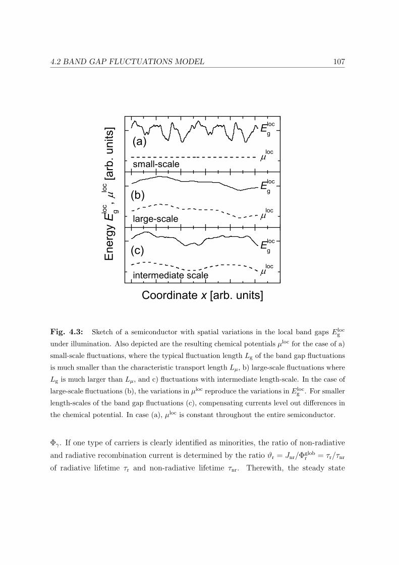
4.2 BAND GAP FLUCTUATIONS MODEL 107
intermediate scale
Elocg
loc
(c)
Coordinate x [arb. units]
large-scale
Elocg
loc
Elocg
(b)
Ene
rgy E
loc
g,
loc [a
rb. u
nits
]
small-scale
(a)loc
Fig. 4.3: Sketch of a semiconductor with spatial variations in the local band gaps Elocg
under illumination. Also depicted are the resulting chemical potentials µloc for the case of a)
small-scale fluctuations, where the typical fluctuation length Lg of the band gap fluctuations
is much smaller than the characteristic transport length Lµ, b) large-scale fluctuations where
Lg is much larger than Lµ, and c) fluctuations with intermediate length-scale. In the case of
large-scale fluctuations (b), the variations in µloc reproduce the variations in Elocg . For smaller
length-scales of the band gap fluctuations (c), compensating currents level out differences in
the chemical potential. In case (a), µloc is constant throughout the entire semiconductor.
Φγ. If one type of carriers is clearly identified as minorities, the ratio of non-radiative
and radiative recombination current is determined by the ratio ϑr = Jnr/Φglobr = τr/τnr
of radiative lifetime τr and non-radiative lifetime τnr. Therewith, the steady state

108 CHAPTER 4. BAND GAP FLUCTUATIONS
condition Jrec = Φγ yields
Φglobr = (1 + τr/τnr)
−1 Φγ ≈ Φγ
ϑr
, (4.10)
where the last term holds if τr À τnr. Following [98], the global radiative recombination
current
Φglobr =
∫ ∞
0
φglobr (E)dE =
2πkBT
h3c2E2
1exp
(−2
(Eg − µ
)kBT − σ2
g
2 (kBT )2
), (4.11)
where E21 is given by
E21 =
(Eg + kBT
)2+ (kBT )2 − σ2
g(2Eg/kBT + 1) + σ4g/(kBT )2, (4.12)
is obtained from integrating Eq. (4.9) over the photon energy E. Using the steady
state condition Eq. (4.10) and solving for µ = µss allows us to derive an expression for
µ = µss under steady state conditions
µss = Eg + kBT ln
(c2h3Φγ
2πϑrkBTE21
)− σ2
g
2kBT. (4.13)
By inserting Eq. (4.13) into Eq. (4.9) we obtain the spectral emission under steady
state conditions
φglobr (E)dE =
Φγ
2ϑrkBTE21
exp
(2EgkBT − σ2
g
2 (kT )2
)×
erfc
(Eg − E√
2σg
)E2exp
(−E
kBT
)dE. (4.14)
4.2.2.2 Large-scale fluctuations
In the large-scale situation, the photogenerated charge carriers recombine before mov-
ing to (distant) regions with different band gap Elocg . Because of this lack of lateral
interaction, each region has to be in a steady state condition, i.e. locally, the total
recombination current J locrec equals the excitation flux Φγ
2. Now, the steady state
condition holds on a local as well as on a global level.
2During PL measurements the sample is illuminated with laser light at a wavelength λ = 488 nm
which corresponds to a photon energy E = 2.54 eV that is much larger than the common average
band gaps of approx. 1.2 eV. Therefore, the local excitation flux Φlocγ = Φγ is roughly independent of
the local band gap Elocg .
4.2 BAND GAP FLUCTUATIONS MODEL 109
Locally, radiative as well as non-radiative recombination currents depend on the
band gap. However, in the case of bulk recombination both currents obey roughly
the same dependency on the band gap. Therewith, the ratio of local radiative and
non-radiative recombination current is independent of the band gap Elocg . For a doped
semiconductor this ratio is determined by the ratio ϑr of radiative lifetime τr and
non-radiative lifetime τnr, which are roughly independent of the band gap (cf. section
4.3.1).
The overall local radiative recombination current
Φlocr =
∫ ∞
E
φlocr (E,E loc
g )dE =Φγ
ϑr
= const. (4.15)
is obtained by integrating Eq. (4.4) over the photon energy dE and equals a con-
stant fraction of the excitation flux. This equation allows us to compute the hitherto
unknown dependence of the local chemical potential µloc on E locg under steady state
conditions with µloc = µlocss . Inserting Eq. (4.4) into Eq. (4.15) yields
Φlocr =
2π
h3c2
∫ ∞
Elocg
E2exp
(−E − µloc
ss
kBT
)dE. (4.16)
Solving this integral and rearranging the result leads to
µlocss (Eloc
g ) = Elocg + kBT ln
(h3c2Φγ
2πϑrkBT
)(4.17)
−kBT ln(
(Elocg + kBT )2 + (kBT )2
).
The knowledge of µlocss (E loc
g ) now allows us to compute the spectral dependence of the
global emission φglobr (E) with help of Eq. (4.7). The resulting integral can only be
solved numerically. However, approximating Elocg with Eg in the logarithmic term in
Eq. (4.17) leads to a simple linear relationship
µlocss (Eloc
g ) = Elocg − const. (4.18)
In the next section I use a generalization of this approach to derive an expression for the
emission under steady state conditions for any length-scale of the band gap fluctuations
with respect to the characteristic transport length.
4.2.2.3 Intermediate length-scale
The last two sections have shown that the splitting of the quasi-Fermi levels is constant
µloc = µ0 in the case of small-scale fluctuations and that it is roughly equal to the local

110 CHAPTER 4. BAND GAP FLUCTUATIONS
band gap reduced by a constant according to µlocss = E loc
g −const in the case of large-scale
fluctuations. In the general case of intermediate length-scales, the simplest approach is
to assume a linear superposition of these two cases namely to assume that µloc consists
of a constant part and a part that depends linearly on the local band gap according to
µloc = µ0 + βElocg (4.19)
where the local chemical potential consists of a constant part µ0 and a part that is
linearly fluctuating with Elocg . The constant factor β with 0 ≤ β ≤ 1 is the quantity that
contains the information about the length-scale of the fluctuations. In the following I
will show that β is equal to the ratio σµ/σg of the standard deviations for band gap
and chemical potential. Subsequently, I derive an expression that relates β to the ratio
Lµ/Lg of the typical length-scales of the respective fluctuations.
Inserting Eq. (4.19) into Eq. (4.1) yields
PG(E locg ) =
1
σg
√2π
exp
(− (
µloc − µ0 − βEg
)2
2β2σ2g
)
=β
σµ
√2π
exp
(− (
µloc − µ)2
2σ2µ
)= βPG(µloc) (4.20)
and therewith the probability density P (µloc) of the chemical potential which is de-
termined by the mean chemical potential µ = µ0 + βEg and the standard deviation
σµ = βσg. Thus, it follows
β = σµ/σg. (4.21)
Next, I derive an expression that relates σµ/σg to the length-scale of the band gap
fluctuations. As pointed out above, I will not attempt to find the exact solution of the
drift-diffusion equation. Instead I provide an approximate approach that makes use of
the Fourier transforms for stochastic processes3.
Basically, the spatial distribution of the chemical potential can be regarded as a
filtered distribution of E locg where the fractions with large spatial frequency have been
cut off. By using some useful theorems of Fourier transforms for stochastic processes
[111] we arrive at the desired relationships between standard deviations and fluctuation
lengths.
3For details concerning Fourier transforms of stochastic processes, see, e.g., Ref. [111].

4.2 BAND GAP FLUCTUATIONS MODEL 111
The spatial distribution of band gaps is not entirely uncorrelated but instead obeys
an autocorrelation function Rg which states that the probability to find a certain band
gap E locg at a given position will also depend on the neighboring band gaps. This
spatial correlation becomes immediately plausible by considering the origin of band
gap fluctuations. For instance, the alloy composition may exhibit lateral fluctuations.
However, there are always compensating processes that prohibit too steep variations.
Mostly, local interaction is restricted to the immediate vicinity of a given location.
With increasing distance the correlation decreases strongly. To obtain integrable func-
tions 4 I assume
Rg(x) = exp
(−x2
L2g
), (4.22)
where x is the distance vector between the two correlated locations and the correlation
length Lg describes the length-scale of the fluctuations. Then the power spectrum of
the distribution
Sg(k) =
∫ ∞
−∞exp (−ikx) Rg(x)dx
=
(Lg√
2
)dim
exp
(−L2
gk2
4
), (4.23)
where k is the spatial frequency, is given by the spatial Fourier transform of Rg (cf.
Ref. [111], p. 319). Depending on the dimension dim of the fluctuations, the integral
in Eq. (4.23) is multidimensional. Integrating over the whole power spectrum yields
the standard deviation
σ2g =
1
2π
∫ ∞
−∞Sg(k)dk (4.24)
as a measure for the overall power contained in the fluctuations (for a mean band gap
Eg = 0) [111, p. 106, 288].
The advantage of using Fourier transforms is that we are now able to deduce the
power spectrum of the chemical potential µloc by applying a filter to the power spec-
trum Sg. If the length-scale of the band gap fluctuations is too short than the chemical
potential does not reproduce the fluctuations exactly but only to an alleviated degree.
4Other approaches such as Rg(x) = exp(−xLg
)qualitatively lead to equivalent results but do not
provide analytic solutions for fluctuations that occur in more than one dimension.

112 CHAPTER 4. BAND GAP FLUCTUATIONS
In the spatial frequency space, this means that band gap fluctuations with high spa-
tial frequency are not reproduced by the chemical potential. Effectively, the power
spectrum of the chemical potential is the result of applying a low-pass filter to the
power spectrum Sg of the band gap distribution. The relevant quantity determining
the filter is the correlation length of the chemical potential Lµ. Band gap fluctuations
with a higher spatial frequency can not be reproduced and are cut off by the filter. At
the moment, Lµ is an unknown quantity. However, as will be shown in section 4.3, Lµ
equals the minority carrier diffusion length Ln if one type of carriers is clearly identified
as minorities. In analogy to Eq. (4.23) I assume a Gaussian filter
F (k) = exp(−L2
µk2/4
)(4.25)
and can thus compute the standard deviation of µloc as
σ2µ =
1
2π
∫ ∞
−∞exp
(−L2
µk2
4
)Sg(k)dk. (4.26)
Performing the integrations in Eq. (4.24) and Eq. (4.26) and combining the two equa-
tions yields the length-scale coefficient
β =σµ
σg
=1
((Lµ/Lg)
2 + 1)dim/4
(4.27)
as a function of the length-scale ratio. Here, dim denotes the dimension of the band
gap fluctuations, that is dim = 2 in the case of lateral fluctuations5. It is readily seen
from Eq. (4.27) that we have β = 0 for Lg ¿ Lµ (small-scale fluctuations) and β = 0
for Lg À Lµ (large-scale fluctuations). Thus, Eq. (4.19) represents a general approach
that applies to all length-scales.
Inserting Eq. (4.19) into Eq. (4.7) and integrating over Elocg yields the global emission
spectrum
φglobr (E)dE =
π
h3c2erfc
(Eg − E + βσ2
g/kBT√2σg
)× (4.28)
E2exp
(−E − µ0 − βEg
kBT+
β2σ2g
2(kBT )2
)dE.
5Note that the choice of the auto-correlation function Rg and especially the filter for µloc is some-
what arbitrary and is not based on physical reasoning. The analytical expression Eq. (4.27) is an
approximation that is not applicable if the actual autocorrelation function and filter function deviate
significantly from the above assumptions.

4.2 BAND GAP FLUCTUATIONS MODEL 113
After integration over the photon energy E and by using the global steady state con-
dition Eq. (4.10) we find
µss0 = (1− β)Eg + kBT ln
(h3c2Φγ
2πϑrkBTE22
)− (1− β)2σ2
g
2kBT(4.29)
with
E22 = (Eg + kBT )2 + (kBT )2 + (1− β)2σ4
g/(kBT )2
+σ2g
(2β − 1− 2Eg(1− β)/kBT
). (4.30)
Inserting these expressions into Eq. (4.28) finally results in the global emission spektrum
φglobr (E)dE =
ϑrΦγ
2kBTE22
exp
(2EgkBT − σ2
g
2(kBT )2
)× (4.31)
erfc
(Eg − E + βσ2
g/kBT√2σg
)E2exp
(− E
kBT
)dE.
With Eq. (4.31) we now have an expression that describes the emission spectrum for
a semiconductor with inhomogeneous band gap for all possible length-scales of the band
gap fluctuations. In the limit of small-scale fluctuations with Lg ¿ Lµ and thus β = 0,
Eq. (4.31) turns into Eq. (4.14). In the case of large-scale fluctuations with Lg À Lµ and
β = 1, the approach (4.19) which results in Eq. (4.31) does not yield the exact situation
as described by Eq. (4.17) where all subdomains are independently under steady state
conditions. Even though the sample is under global steady state conditions, the local
steady state conditions are not necessarily fulfilled. However, Eq. (4.31) provides a
reasonable approximation which is valid as long as σg ¿ Eg. Figure 4.4 demonstrates
that for a medium band gap Eg = 1 eV the differences between the emission spectra
according to the numerical solution of Eq. (4.7) with µloc given by Eq. (4.17) on the one
hand and the analytical approximation Eq. (4.31) one the other hand are negligible for
σg < 100 meV.
4.2.3 Discussion
Figure 4.2b depicts the emission current in the case of small-scale band gap fluctu-
ations according to Eq. (4.14) with Eg = 1 eV and σg = 50 meV and 100 meV. The
figure shows how band gap fluctuations with the resulting broadening of the absorption
transition also broaden the emission peak. Due to the exponential dependence of the

114 CHAPTER 4. BAND GAP FLUCTUATIONS
0.9 1.0 1.1
0.2
0.4
0.6
numerical
g =50 meV
g =100 meV
E
mis
sion
Flu
x
Em [a
rb. u
nits
]
Photon Energy E [eV]
analytical
Fig. 4.4: Luminescence spectra in the case of large-scale fluctuations. Comparison between
numerical solution of Eq. (4.7) with µloc = µlocss according to Eq. (4.17) (dashed lines) and the
analytical approximations Eq. (4.31) with β = 1 (solid lines) for Eg = 1 eV and σg = 50meV
or 100 meV. For standard deviations σg larger than 100 meV the difference between the
analytical approximation and the the numeric solution becomes more pronounced.
emission spectrum on the photon energy, a small increase of the absorption at lower
energies results in an amplified increase of the corresponding emission, whereas a small
increase of the absorption at higher energies results only in a reduced increase of the
emission. Therefore, the position of the emission peak is shifted towards lower energies
for more inhomogeneous samples.
Figure 4.2c displays the emission spectrum for large-scale fluctuations according to
Eq. (4.31) with β = 1. As in the case of small-scale fluctuations, the emission peak
of an increasingly inhomogeneous sample is broadened. But whereas small-scale band
gap fluctuations lead to a shift of the emission peak towards lower photon energies,
large-scale fluctuations leave the position of the peak unchanged at the average band
gap Eg.

4.3 NUMERICAL APPROACH 115
Note that for identical σg the only difference between the spectra in Figs. 4.2b and
4.2c is the position of the peak. Spectral shape and magnitude of the spectra and, as a
consequence, the integrated emission spectra are the same. Since both cases are under
steady state conditions, the global recombination current is equal to the impinging
photon flux and it holds in all cases Φglobr = Φγ/ϑr according to Eq. (4.10).
Therefore, the position of the emission peak relative to the absorption edge yields
information about the length-scale of the band gap fluctuations. Fitting Eq. (4.3) and
Eq. (4.31) to a set of experimental absorptance and PL data yields the average band
gap Eg, the standard deviation σg, and the length-scale ratio Lµ/Lg. We can thus
extract extent and length-scale of the measured inhomogeneities from experimental
absorption and emission data, as will be shown in section 4.4. First, however, we need
to analyze the relationship between the fluctuation length Lµ of the chemical potential
and the minority carrier diffusion length Ln.
4.3 Numerical approach
In the previous sections I have only provided hand-waving arguments for the alleged
agreement of the correlation length Lµ of the chemical potential µ with the diffusion
length Ln in the situation where one type of carriers is clearly defined as minorities.
As plausible as the reasoning might seem - the compensating lateral currents are not
driven by carrier diffusion alone. The band gap fluctuations also lead to local quasi-
electric fields that cause minority carrier drift currents. Drift and diffusion currents
both depend on the strength and the length-scale of the band gap fluctuations, i.e. on
σg and Lg. It is thus not completely clear, whether the resulting correlation length Lµ
really is identical to the diffusion length Ln.
This section provides a numerical solution of the drift-diffusion equation to verify
the results of the above analytical model and to show that the diffusion length in-
deed represents a very good indicator to approximate the correlation length Lµ of the
chemical potential.
Osvald [109] investigates a very similar problem consisting of a Schottky diode with
spatial variations of the Schottky barrier. However, while he needs to simultaneously
solve the drift-diffusion equation and the Poisson equation to solve the problem , here,
the band gap is not only preset as a boundary condition but throughout the entire

116 CHAPTER 4. BAND GAP FLUCTUATIONS
sample. Thus, the band diagram is already known and we do not need to additionally
solve the Poisson equation.
4.3.1 Formulation of the problem
For the sake of simplicity, I assume that all band gap fluctuations occur in the con-
duction band as depicted in Fig. 4.5. The valence band features no variations and is
constant throughout the entire semiconductor. Moreover, I treat the problem as a
pure minority carrier problem. The quasi Fermi level EFp of the holes is invariant as
well. Thus, the majority carrier concentration does not fluctuate and is given by the
doping density NA. Furthermore, the fluctuations of the conduction band are assumed
to be sufficiently small, such that even in regions with small band gap, the electron
concentration is still decisively smaller than the hole concentration.
The simplification of assuming that all band gap fluctuations occur in the conduction
band, is only a special case of the general case depicted in Fig. 4.1. Therewith, the
numerical results obtained in this section are not as general as the results obtained with
the analytical model. However, the approximation is sufficient to show the relevance
of the diffusion length for the length-scale of the chemical potential.
In general, the drift-diffusion equation for the minority carriers can be written as
[112]
∇ (n0∇u)− n0u
L2n
= − g
Dn
. (4.32)
Here, Dn is the electron diffusion constant and g(x) is the generation rate. The equi-
librium electron concentration is determined by the local band gap according to
n0(x) =n2
i
p0
=NCNV
NA
exp
(−Eg(x)
kBT
). (4.33)
The normalized excess electron concentration is given by
u(x) =n(x)− n0(x)
n0(x). (4.34)
Equation (4.32) assumes a spatially constant lifetime τn and, therewith, a constant
diffusion length Ln. Such an assumption is only valid if the lifetime is independent of
the band gap.
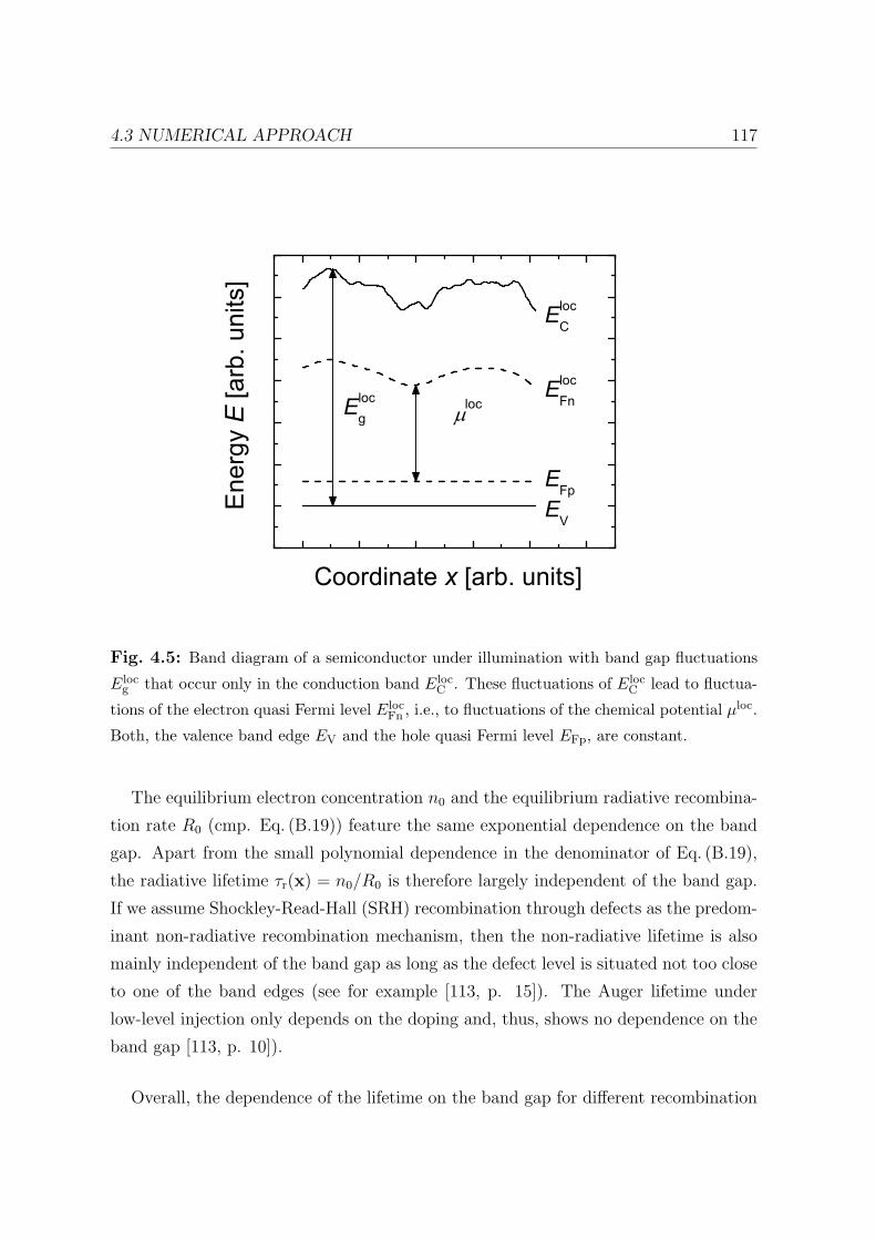
4.3 NUMERICAL APPROACH 117
EV
EFp
ElocFnEloc
g
Coordinate x [arb. units]
E
nerg
y E
[arb
. uni
ts]
ElocC
loc
Fig. 4.5: Band diagram of a semiconductor under illumination with band gap fluctuations
Elocg that occur only in the conduction band Eloc
C . These fluctuations of ElocC lead to fluctua-
tions of the electron quasi Fermi level ElocFn , i.e., to fluctuations of the chemical potential µloc.
Both, the valence band edge EV and the hole quasi Fermi level EFp, are constant.
The equilibrium electron concentration n0 and the equilibrium radiative recombina-
tion rate R0 (cmp. Eq. (B.19)) feature the same exponential dependence on the band
gap. Apart from the small polynomial dependence in the denominator of Eq. (B.19),
the radiative lifetime τr(x) = n0/R0 is therefore largely independent of the band gap.
If we assume Shockley-Read-Hall (SRH) recombination through defects as the predom-
inant non-radiative recombination mechanism, then the non-radiative lifetime is also
mainly independent of the band gap as long as the defect level is situated not too close
to one of the band edges (see for example [113, p. 15]). The Auger lifetime under
low-level injection only depends on the doping and, thus, shows no dependence on the
band gap [113, p. 10]).
Overall, the dependence of the lifetime on the band gap for different recombination
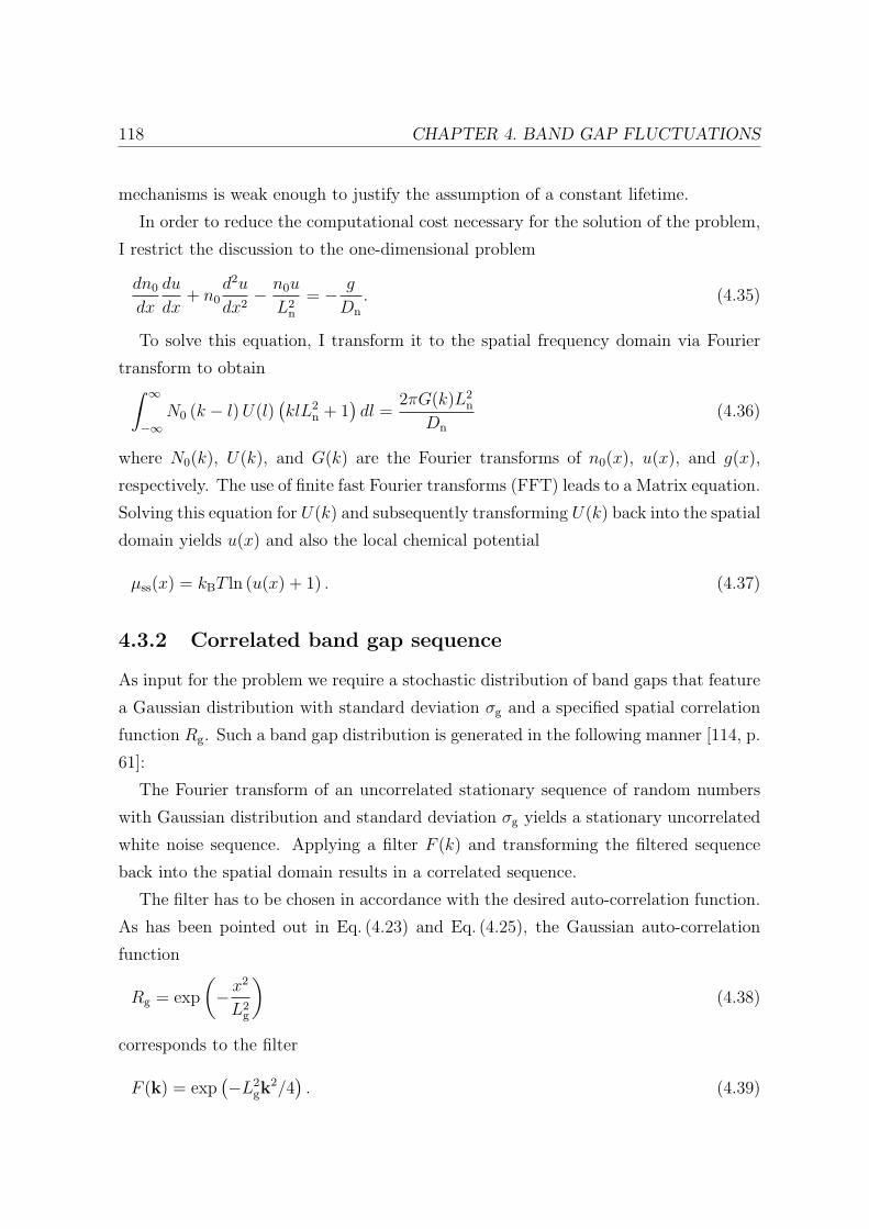
118 CHAPTER 4. BAND GAP FLUCTUATIONS
mechanisms is weak enough to justify the assumption of a constant lifetime.
In order to reduce the computational cost necessary for the solution of the problem,
I restrict the discussion to the one-dimensional problem
dn0
dx
du
dx+ n0
d2u
dx2− n0u
L2n
= − g
Dn
. (4.35)
To solve this equation, I transform it to the spatial frequency domain via Fourier
transform to obtain∫ ∞
−∞N0 (k − l) U(l)
(klL2
n + 1)dl =
2πG(k)L2n
Dn
(4.36)
where N0(k), U(k), and G(k) are the Fourier transforms of n0(x), u(x), and g(x),
respectively. The use of finite fast Fourier transforms (FFT) leads to a Matrix equation.
Solving this equation for U(k) and subsequently transforming U(k) back into the spatial
domain yields u(x) and also the local chemical potential
µss(x) = kBT ln (u(x) + 1) . (4.37)
4.3.2 Correlated band gap sequence
As input for the problem we require a stochastic distribution of band gaps that feature
a Gaussian distribution with standard deviation σg and a specified spatial correlation
function Rg. Such a band gap distribution is generated in the following manner [114, p.
61]:
The Fourier transform of an uncorrelated stationary sequence of random numbers
with Gaussian distribution and standard deviation σg yields a stationary uncorrelated
white noise sequence. Applying a filter F (k) and transforming the filtered sequence
back into the spatial domain results in a correlated sequence.
The filter has to be chosen in accordance with the desired auto-correlation function.
As has been pointed out in Eq. (4.23) and Eq. (4.25), the Gaussian auto-correlation
function
Rg = exp
(−x2
L2g
)(4.38)
corresponds to the filter
F (k) = exp(−L2
gk2/4
). (4.39)

4.3 NUMERICAL APPROACH 119
Using this filter allows the comparison between the numerical results and the results
from the analytical model which is based on the Gaussian auto-correlation function.
Performing an inverse Fourier transform of the filtered sequence and adding the
mean band gap Eg finally yields the desired Gaussian band gap distribution with the
mean value Eg, the standard deviation σg, and the Gaussian auto-correlation function
Eq. (4.38).
4.3.3 Discussion
Figure 4.6 exemplarily displays one-dimensional spatial fluctuations of the band gap
energy Eg versus the spatial coordinate x normalized to the fluctuation length (cor-
relation length) Lg (bold line). The fluctuations in Fig. 4.6 feature a Gaussian auto-
correlation function and a standard deviation σg = 50 meV. For simplicity, the band
gap is corrected by the mean band gap Eg, i.e., the plot shows Eg − Eg.
The figure also displays the resulting fluctuations of the chemical potential µ − µ
corrected by the mean chemical potential µ for different length-scale ratios Ln/Lg of
diffusion length Ln and fluctuation length Lg.
For very small diffusion lengths Ln < 0.3 Lg (large-scale fluctuations), the chemical
potential essentially reproduces the spatial fluctuations of the band gap. With increas-
ing diffusion length, lateral currents increasingly compensate the fluctuations of the
chemical potential. For Ln > 100 Lg, i.e., small-scale fluctuations with a length-scale
that is much smaller than the diffusion length, µ hardly features any fluctuations at
all.
Figure 4.7 depicts the dependence of the ratio β = σµ/σg of the standard deviations
σµ and σg on the length-scale ratio Ln/Lg for different magnitudes of the band gap
fluctuations in terms of the standard deviation σg.
The analytical model Eq. (4.27) with the fluctuation length of the chemical potential
Lµ = Ln being equal to the diffusion length Ln predicts that β is unity for Ln < Lg and
drops sharply once the diffusion length exceeds the fluctuation length (dashed line).
This dependence is independent of the magnitude of σg.
In contrast, the numerical results unveil that β does depend on σg. While numerical
and analytical results agree reasonably well for small fluctuations with σg ≤ 25 meV,
the numerically obtained curves exhibit a broadened decline.
At a small amplitude, fluctuations thus seem to enhance lateral compensating cur-

120 CHAPTER 4. BAND GAP FLUCTUATIONS
0 10 20 30
-100
-50
0
50
100
300
30
3
Ln / Lg = 0.3
E
nerg
y E
g, [m
eV]
Spatial Coordinate x / Lg
Eg
Fig. 4.6: Band gap fluctuations and resulting fluctuations of the chemical potential versus
the spatial coordinate x normalized to the fluctuation length Lg for a standard deviation
σg = 50meV. The bold line represents the band gap fluctuations Eg − Eg corrected by
the mean band gap Eg. With increasing length-scale ratio Ln/Lg of diffusion length and
fluctuation length, the chemical potential µ− µ corrected by the mean chemical potential µ
can not follow the band gap fluctuations.
rents, resulting in β being smaller than predicted by the analytical model. For increas-
ing magnitude σg of the fluctuations, however, this effect is reversed and β is larger
than the analytical β obtained with Eq. (4.27).
Overall, the simulations show that
(i) the analytical model is a good approximation for the relation between the stan-
dard deviation ratio β = σµ/σg and the length-scale ratio Ln/Lg as long as the
magnitude of the band gap fluctuations does not exceed σg ≈ 50 meV, and that
(ii) the diffusion length indeed is the crucial parameter that determines the fluctua-
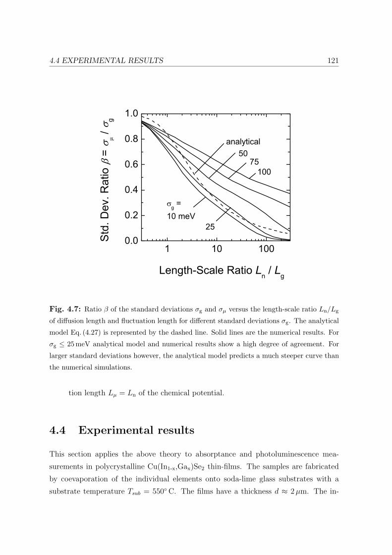
4.4 EXPERIMENTAL RESULTS 121
1 10 1000.0
0.2
0.4
0.6
0.8
1.0
10075
50
25
g =10 meV
analytical
S
td. D
ev. R
atio
=
/
g
Length-Scale Ratio Ln / Lg
Fig. 4.7: Ratio β of the standard deviations σg and σµ versus the length-scale ratio Ln/Lg
of diffusion length and fluctuation length for different standard deviations σg. The analytical
model Eq. (4.27) is represented by the dashed line. Solid lines are the numerical results. For
σg ≤ 25meV analytical model and numerical results show a high degree of agreement. For
larger standard deviations however, the analytical model predicts a much steeper curve than
the numerical simulations.
tion length Lµ = Ln of the chemical potential.
4.4 Experimental results
This section applies the above theory to absorptance and photoluminescence mea-
surements in polycrystalline Cu(In1-x,Gax)Se2 thin-films. The samples are fabricated
by coevaporation of the individual elements onto soda-lime glass substrates with a
substrate temperature Tsub = 550 C. The films have a thickness d ≈ 2 µm. The in-

122 CHAPTER 4. BAND GAP FLUCTUATIONS
vestigated samples are either prepared in a three-stage process described in detail in
Ref. [115] or in a single-stage process which means coevaporation of all elements at
constant rates. All samples have a slightly copper-poor final composition. I vary the
relative Ga content x from x = 0 to x = 1. The three-stage samples are covered with a
50 nm thick CdS layer deposited from a chemical bath in order to reduce surface recom-
bination during PL measurements. The CdS layer has a band gap of approx. 2.4 eV. It
passivates the surface and therewith substantially improves the luminescence signals.
The single-stage samples, which are only used for absorptance measurements, do not
have such a protective layer.
Absorptance spectra are obtained from room temperature reflection and transmis-
sion measurements as described in Ref. [72]. Photoluminescence (PL) spectra are
measured at room temperature under monochromatic excitation at λ = 514 nm with
an areal power density of 300 mW/ cm2 as described in Ref. [116].
The fabricated three-stage CIGS thin films exhibit three different Ga contents x =
0.3, x = 0.4 and x = 0.5. Figures 4.8a-c show the measured absorptance and PL
spectra. Also displayed are the theoretical curves obtained from simultaneously fitting
Eq. (4.3) to the measured absorptance data and Eq. (4.31) to the measured PL data.
The fit-parameters are the mean band gap Eg, the standard deviation σg, the length-
scale coefficient β and an additional factor for adjusting the magnitude of the emission
spectra. In accordance with the literature [117], the average band gap increases with
the Ga content. The obtained medium band gaps are Eg = 1.15, 1.19, and 1.24 eV for
x = 0.3, 0.4 and 0.5. These results are consistent with the band gaps obtained from
quantum efficiency measurements of solar cells fabricated from absorbers processed in
the same run. The standard deviations resulting from the fits are σg = 48, 50, and
62 meV. Figure 4.9 displays the values as solid triangles. For the length-scale coefficient
we obtain β = 0 in all cases, which means that the length-scale Lg of the observed band
gap fluctuations is much smaller than the characteristic transport length Lµ. Since all
prepared samples are p-type semiconductors, Lµ equals the electron diffusion length
Ln. Note that some systematic deviations of the experimental in Fig. 4.8 are due to
parasitic absorption as discussed in section 4.5.1 and to optical interference effects as
discussed in section 4.5.3.1.
We have also fabricated CIGS thin films in a single-stage process with varying
gallium content x =Ga/(In+Ga) from x = 0 to x = 1 from pure CuInSe2 to pure

4.4 EXPERIMENTAL RESULTS 123
0.20.40.60.8
0.20.40.60.8
0.20.40.60.8
1.0 1.2 1.4
10-3
10-2
x = 0.5
(c)
Photon Energy E [eV]
10-3
10-2
x = 0.4
(b)
Em
issi
on F
lux
glob
r [a
rb. u
nits
]
10-3
10-2
(a)
x = 0.3
Abs
orpt
ance
a
Fig. 4.8: Absorptance and photoluminescence spectra of CIGS thin films processed in a
three-stage process with different gallium content x. Fitting Eq. (4.3) and Eq. (4.31) (solid
lines) to the experimental data (symbols) simultaneously yields the fit-parameters Eg = 1.15,
1.19, and 1.24 eV and σg = 48, 50, and 62 meV for x = 0.3, 0.4, and 0.5. All data-sets exhibit
small-scale fluctuations with β = 0, i. e. Lg ¿ Ln.
CuGaSe2 and analyzed the absorptance spectra of these films by fitting Eq. (4.3) to the
measured data. As for the three-stage samples, Eg increases with x. We obtain Eg =
1.0, 1.13, 1.29, 1.41, and 1.66 eV for x = 0, 0.25, 0.5, 0.75, and x = 1. The standard
deviations obtained from fitting the measured absorptance spectra are displayed in
Fig. 4.9 as solid squares.

124 CHAPTER 4. BAND GAP FLUCTUATIONS
0.0 0.2 0.4 0.6 0.8 1.0
20
40
60
abs., num. model
absorption
S
tand
ard
Dev
iatio
n g [m
eV]
Gallium Content x
abs. / PL
Fig. 4.9: Standard deviation σg of the local band gap energy Elocg in dependence of the
relative gallium content x as obtained from the combined absorptance/photoluminescence
fits displayed in Fig. 4.8 (solid triangles), and from fitting absorptance spectra of single-layer
samples with either Eq. (4.3) (solid squares) or a numerical approach that considers coherent
optics (open squares). The solid lines are a guide to the eye. For the ternary compounds
CuInSe2 and CuGaSe2 the fluctuations are minimal. This finding indicates alloy disorder as
one possible source of inhomogeneities.
4.5 Discussion
4.5.1 Length-scale of band gap fluctuations
The simultaneous analysis of absorptance and emission spectra relies on the assumption
that light emission is associated with fundamental light absorption, i.e. that the dom-
inant radiative recombination mechanism is band to band recombination. In general,
the measured luminescence spectra are a superposition of all possible optical transi-
tions. Especially donor-acceptor transitions are well-known in heavily compensated
4.5 DISCUSSION 125
semiconductors like CIGS [118–121]. However, such transitions are usually analyzed
at temperatures below T = 20 K. At such low temperatures, the Fermi-distribution
is very steep and therefore, the occupation probability of states below the conduction
band edge is much higher than the occupation probability of higher energy levels. Con-
sequently, transitions like donor-acceptor transitions gain importance at low tempera-
tures. At room temperature, the Fermi-distribution is quite broad and it is reasonable
to assume band to band recombination as the dominant radiative recombination path.
Recently, Kirchartz et al. [122, 123] have shown in electroluminescence measurements
that the dominant luminescent emission changes from a broadened donor-acceptor
pair recombination at temperatures below T = 140 K to band to band recombination
at temperatures above T = 200 K. Indications for this change are the higher peak
energies of the emission peak as well as the absence of an intensity-dependent blueshift
of the spectra at temperatures above 200 K. Another indication for the validity of this
assumption is the consistency of the standard deviations σg obtained from absorptance
and luminescence fits of the three-stage samples, which are obtained in different energy
ranges. Whereas σg determines the slope of the absorption edge in an energy range
around the mean band gap Eg, it determines the low-energy flank of the luminescence
peak which is located more than 100 meV below the absorption edge.
The experimentally observed shifts between luminescence peak and absorption edge
displayed in Fig. 4.8 yield the length-scale coefficient β = 0 in all cases. Therefore, I
conclude that all investigated samples feature fluctuations that occur on a length-scale
which is much smaller than the electron diffusion length Ln of Ln ≈ 1 µm. Reasonable
fit results could only be obtained when using β < 0.1. Via Eq. (4.27) and assuming two-
dimensional band gap fluctuations, this β-value corresponds to a diffusion length Ln
that is at least ten times larger than the fluctuation length Lg. Moreover, comparison
with the numerical results in Fig. 4.7 suggest that, with σg ≥ 50 meV, the diffusion
length needs to be more in the order of 100 times larger than the fluctuation length
to obtain such low values for β. Therefore, even accounting for the influence of donor-
acceptor pair recombination, which would also shift the emission peak towards lower
energies, would not alter the result of Lg ¿ Ln. The observed fluctuations are definitely
small-scale fluctuations.
In the case of small-scale band gap fluctuations, the electron and the hole population
in the entire semiconductor are each described by homogeneous quasi-Fermi levels.

126 CHAPTER 4. BAND GAP FLUCTUATIONS
Therefore, the chemical potential µ of photons is uniform throughout the sample and
Wurfel’s generalization of Kirchhoff’s law holds for the global light emission spectrum.
Local and global emission spectra are determined by the product of absorptance and
black body spectrum according to Eq. (4.4).
In contrast, any departure from the small-scale limit leads to a spatially nonuniform
µ(x) and Eq. (4.4) is only valid locally. Thus, a way to access the length-scale of
inhomogeneities is to test the validity of Eq. (4.4) for global absorption/emission data.
Figure 4.10 compares the measured absorptance data (open squares) of a three-stage
sample with x = 0.4 to the data (open triangles) that are reconstructed from the PL
spectra [124,125] by inversion of Eq. (4.4) according to
aloc(E) ∝ E−2exp
(E
kBT
)dΦloc
r (E)
dE. (4.40)
Additionally, Fig. 4.10 displays the theoretical fit to Eq. (4.3) (solid line) as performed
in Fig. 4.8b. All three curves show a good agreement for E > 1.1 eV. In the case of
fluctuations on a larger length-scale, the absorption data reconstructed with help of
Eq. (4.40) and the measured absorption data would not show such an agreement. In
that case, the luminescence is no longer the product of absorptance and black-body
spectrum, but instead the modified spectrum according to Eq. (4.31) with β 6= 0.
To underline the inapplicability of Kirchhoff’s law in the large-scale limit, I com-
pute the large-scale emission spectrum according to Eq. (4.31) with β = 1 using the
parameters Eg = 1.19 eV and σg = 50 meV from the fit of the absorption data (cf.
Fig. 4.8b). The spectral position of the large-scale emission peak is at higher energies
than the measured PL peak and therewith, reconstructing the absorptance spectra with
help of Eq. (4.40) results in a shifted absorption edge (dotted line in Fig. 4.10) that is
not in agreement with the measured absorptance spectrum. Thus, the consistency of
PL and absorption data at energies E > 1.1 eV unveils the small-scale nature of the
fluctuations.
It is however also evident that at energies E ≤ 1.1 eV the absorption of the sample
is far larger than would be expected from the emission data. I observe such a parasitic
absorption, which is also heavily influenced by interference patterns, in all our samples.
Similar results were also reported earlier for samples from other sources [126]. Obvi-
ously, this absorption stems from parts of the samples that do not contribute at all to
the radiative emission, i.e., parts with negligible chemical potential µ of the photons.

4.5 DISCUSSION 127
0.01
0.1
1
1.0 1.2
= 0 = 1
x = 0.4
Photon Energy E [eV]
directmeasurement
from PL
Abs
orpt
ance
a
Fig. 4.10: Absorptance spectrum of a Cu(In1-x,Gax)Se2 three-stage sample with a gallium
content x = 0.4. The spectrum obtained from transmission and reflection measurements
(open squares) exhibits pronounced sub-band gap absorption. The spectrum reconstructed
from PL measurements (open triangles) does not show this parasitic sub-band gap absorp-
tion. The theoretical absorptance curve from Fig. 4.8b is displayed as well (solid line). It
nicely represents the absorptance spectrum extracted from the luminescence measurements.
The consistency of measured and reconstructed absorptance spectrum underlines the validity
of Wurfel’s generalization of Kirchhoff’s law, which only holds in the case of small-scale fluc-
tuations. Assuming large-scale fluctuations would result in an absorptance spectrum which
is substantially shifted towards higher energies (dotted line).
Most likely, this ’dark matter’ corresponds to photovoltaically inactive phases with a
broad-range absorption. Whether or not these phases play a significant role for the
device performance is unclear up to now.
128 CHAPTER 4. BAND GAP FLUCTUATIONS
4.5.2 Origin of band gap fluctuations
The dependence of the standard deviations σg on the Ga/(In+Ga)-ratio x as depicted
in Fig. 4.9 shows that the pure alloys CuInSe2 and CuGaSe2 are less inhomogeneous
than the quaternary alloys. Thus, alloy disorder is clearly one source of the inhomo-
geneities detected by our experiments. This conclusion is also compatible with the fact
that we are dealing with fluctuations on a length-scale of less than 100 nm because
statistical alloy disorder occurs on a length-scale of a few unit cells of the crystal struc-
ture. Orgassa [72] analyzed the band tails of the absorption coefficient and reports an
analogue dependence of the Urbach energy on the gallium content. Along a similar line,
the broadening of the transition peaks in the admittance spectra in Cu(In,Ga)(S,Se)2
solar cells was found to increase with increasing In/Ga and/or S/Se alloying [127].
The fact that maximum inhomogeneity is achieved at x = 0.75 instead of x = 0.5
and the fact that σg is larger in CuGaSe2 than in CuInSe2 points to a second source of
inhomogeneities. In general, the material quality decreases in Cu(In,Ga)Se2 alloys with
increasing Ga content such that structural defects on a small length-scale contribute to
the inhomogeneity of the Cu(In,Ga)Se2 thin-films and significantly reduce the electronic
film quality [128,129].
Also, Cu-poor/Cu-rich nanodomains as recently found by transmission electron mi-
croscopy combined with x-ray energy-dispersive spectroscopy [100] might contribute
to band gap fluctuations. Such a conclusion would fit to the observation that band
gap fluctuations in CuInSe2 films detected by absorption measurements increase with
decreasing Cu-content [130].
In contrast to small-scale fluctuations, there are also variations of the electronic
properties of Cu(In,Ga)Se2 thin films on a length-scale of 3 − 20 µm as detected by
spatially resolved PL measurements [131] and electron-beam induced voltage analysis
[132]. These variations most likely originate from variations of the electronic material
quality and are not or only slightly related to variations of the fundamental band gap.
Grabitz finds Voc variations with a standard deviation σ = 70−85 mV. Looking at the
local PL spectra measured by Gutay and Bauer (cf. Fig. 3c in Ref. [131]) unveils that
the spectral position of the maxima of those peaks differs only slightly. The authors find
that the associated band gap energies vary by at most 15 meV. In contrast, the width
of each local spectrum (taken with a spatial resolution of less than 1 µm) corresponds
to a standard deviation σg ≈ 35 meV if analyzed by fitting the present Eq. (4.14) to the

4.5 DISCUSSION 129
data in Fig. 3c in Ref. [131]. We may thus conclude that in those sub-micron-resolution
PL spectra the band gap fluctuations below the resolution limit are larger than those
that are resolved in these measurements. Conversely, the chemical potential µloc in
terms of the PL-yields, which varies by a factor of ten, shows significant fluctuations
on a larger length-scale of 3− 20 µm which are not caused by band gap fluctuations.
From the differences of the observed length-scales, I conclude that there are various
types of inhomogeneities in CIGS absorber films. Localized disorder such as composi-
tional or alloy disorder results in small-scale fluctuations of the band gap. On a larger
length-scale the chemical potential µloc shows additional fluctuations due to variations
in the local electronic quality of the absorber films.
In his PhD thesis [133, p. 97], Grabitz discusses different types of inhomogeneities
in CIGS absorber layers and possible causes of the inhomogeneities. He also describes
which method can be used to characterize different types of inhomogeneities. For
the analysis of large-scale fluctuations of electronic material properties, he develops
a multi-diode model that assigns different diode properties to regions with varying
electronic material quality [133, p.33], [103,134]. However, such a model is only suited
for large-scale inhomogeneities that do not require 2 or 3-dimensional device simulation.
Applying the model to temperature-dependent current-voltage measurements of CIGS
solar cells, Grabitz finds standard deviations σ ≈ 140 meV in the activation energy
that describes the local recombination behavior.
One important question arising from these different types of inhomogeneities is in
how far fluctuations of the chemical potential that originate from causes other than
band gap fluctuations influence the measured luminescence spectra.
The theoretical model developed in section 4.2 assumes that all regions with identical
local band gap Elocg also exhibit identical local chemical potential µloc(E loc
g ).
If µloc features additional fluctuations, this implies that for a given Elocg , different
regions can still exhibit different µloc. The average chemical potential µav(Elocg ) of these
regions differs from the chemical potential µmodel(Elocg ) which would have corresponded
to that band gap if no additional fluctuations had been present. However, under
the assumption that the additional fluctuations of µloc are completely uncorrelated to
fluctuations in E locg , the relationship between the average chemical potential µav(E
locg )
and µmodel(Elocg ) is independent of the band gap energy.
Therefore, the resulting global luminescence spectrum changes only in magnitude

130 CHAPTER 4. BAND GAP FLUCTUATIONS
but not in spectral position. This means that PL measurements on an arbitrary yield
scale are not influenced by fluctuations of electronic material properties which cause
fluctuations in the chemical potential. The spectral position of the luminescence peak
is only determined by fluctuations of optical properties, e.g. fluctuations of the band
gap energy which lead to fluctuations of the absorptance spectrum.
4.5.3 Model refinements
This section introduces some refinements of the relatively simple analytical model pre-
sented in section 4.2. The first section deals with fluctuations of the band gap over the
film depth, incomplete absorption and optical interference effects. Subsequently, the
implications of vertical gradings in the gallium content which lead to vertical band gap
gradings are analyzed.
4.5.3.1 Coherent optical analysis
The presented analytical model only features lateral fluctuations and assumes a con-
stant band gap throughout the film depth. Such an assumption is justified as long
as the length-scale of the fluctuations is larger than the film thickness. However, the
analysis of experimental data results in length-scales in the sub-micron regimes which
is much smaller than the film thickness of approximately 2 µm. In addition, the absorp-
tance and luminescence spectra feature pronounced interference patterns that hamper
the interpretation of the data. A more accurate approach therefore requires the treat-
ment of vertical band gap fluctuations and a coherent optical approach that accounts
for non-ideal absorption and interference effects.
In direct semiconductors the absorption coefficient α obeys a square root-depen-
dence on the photon energy E according to α(E) = α0
√(E − Eg)/kBT where α0 is
the absorption coefficient at E = Eg + kBT (cmp. Tab. 3.2). In the small-scale limit
of an inhomogeneous absorber with a band gap that is stochastically fluctuating over
the absorber depth I define the effective absorption coefficient as
αeff(E) =
∫ ∞
−∞α0
√(E − Eloc
g )/kBTP (Elocg )dE loc
g . (4.41)
In this case, Elocg denotes the (fluctuating) band gap over the absorber depth. Note
that laterally, the effective absorption coefficients are identical so that we do not need
an additional lateral averaging.

4.5 DISCUSSION 131
For a system of plane-parallel thin layers, the absorptance can be calculated in a
coherent optical analysis by making use of the matrix formalism for the propagation
of electro-magnetic waves in stacks of homogeneous materials [72, 135]. With help of
the effective absorption coefficient αeff we thus numerically calculate the small-scale
limit of the coherent absorptance. Note that the coherent optical analysis can also be
carried out by calculating the coherent local absorptance with a locally well defined
αloc and inserting that value into Eq. (4.3).
Figure 4.11a exemplarily displays the measured absorptance data of a single-stage
sample with x = 0.5 and the theoretical curves from fitting Eq. (4.3) or the coherent
optical computation to the measured data. Accounting for non-ideal local absorption
instead of the step-function utilized in Eq. (4.3) leads to far better fits to the experi-
mental data. However, the standard deviations σg obtained from using the coherent
optical model are only about 5 meV smaller than those obtained from the analytical
model (cf. Fig. 4.9 (open squares)). This result demonstrates the reliability of the
analytical model with respect to determining the extent of band gap fluctuations. For
the reliability of the fit results it is crucial though, not to fit the whole data range but
only a section that features no interference patterns.
4.5.3.2 Band gap grading
Another aspect to be discussed here is a nonuniform gallium content throughout the
film depth. Samples grown in a three-stage process exhibit a gallium grading over the
depth of the films [115, 136, 137]. The gallium content and therewith the band gap is
larger at the back of the film than towards the film surface. Therefore, the absorption
coefficient α(E) for a given energy E decreases towards the substrate [88,91].
Figure 4.11b demonstrates the impact of a band gap grading on the absorptance
spectrum. The figure depicts the absorptance for different ∆Eg = Eg(z = d)−Eg(z =
0) = 0 meV, 50 meV, and 300 meV, where z is the spatial coordinate over the absorber
depth6 and d is the absorber thickness. The parameters for the simulation are the
surface band gap Eg(0) = 1 eV, the thickness d = 2 µm, and an absorption coefficient
α(E, z) = 104 cm−1√
(E − Eg(z))/(kBT ).
The effect of the grading is very similar to the effect of band gap fluctuation. At
6In contrast to the notation in chapter 3, the vertical coordinate is denoted as z because here, x
already denotes the Ga content.

132 CHAPTER 4. BAND GAP FLUCTUATIONS
1.0 1.2 1.4 1.6
0.2
0.4
0.6
0.8
1.0 1.2
0.2
0.4
0.6
0.8
coherent optics
analytical model
Abs
orpt
ance
a
Photon Energy E [eV]
x = 0.5
300 meV
50 meVEg =
0
Abs
orpt
ance
a
Fig. 4.11: a) Absorptance spectrum of a single-layer sample with Ga content x = 0.5.
Fitting Eq. (4.3) to the measured data (open triangles) yields the dotted line. Accounting
for optical interferences leads to the solid line. The fit parameters are Eg = 1.29 eV and
σg = 45meV when using Eq. (4.3) and σg = 40 meV when accounting for interferences. b)
Simulated absorptance spectrum for different gradings from ∆Eg = Eg(d) − Eg(0) = 0,
50meV, and 300 eV. The thickness is d = 2µm, the surface band gap is Eg(0) = 1 eV, and
the absorption coefficient is given by the square-root dependence of a direct semiconductor
as described in the text. Particularly in the energy range Eg(0) < E < Eg(d) the grading
decreases the absorptance.
energies Eg(0) < E < Eg(d), the absorption is reduced which leads to a broadening
of the absorption edge. Three-stage samples that are grown at a constant Ga rate,
typically feature band gap gradings F ≈ 25 meV/ µm [88,115]. Such gradings result in
a broadening which is comparable to the broadening induced by band gap fluctuations
with standard deviations σg ≈ 15 meV. The grading can be enhanced by intentionally
decreasing the Ga rate during absorber deposition. Such samples feature gradings up
to F ≈ 150 meV/ µm which correspond to standard deviations σg ≈ 40 meV.
Obviously, this finding has serious consequences for the interpretation of the ob-

4.5 DISCUSSION 133
tained standard deviations in terms of lateral band gap fluctuations in the case of
three-stage samples. The standard deviations displayed in Fig. 4.9 as solid triangles
are obtained under the assumption that the complete broadening is a result of band
gap fluctuations only. Thus, they represent maximum values for the band gap inho-
mogeneities. Taking into account the band gap grading would result in significantly
smaller standard deviations. Therewith, the grading provides a qualitative argument
why the standard deviations of three-stage samples are larger than the ones obtained
from single stage samples.
4.5.4 Implications for solar cell performance
Inhomogeneous samples exhibit absorption at lower photon energies. Due to the ex-
ponential dependence of all recombination mechanisms that are governed by the band
gap, the overall recombination current in an inhomogeneous semiconductor will thus
be larger than in a homogeneous sample with a band gap Eg that equals the average
band gap Eg of the inhomogeneous sample. This increase of the total recombination
current leads to a reduced open circuit voltage [98]
V inhomoc ≈ V hom
oc − σ2g
2kBTq(4.42)
of inhomogeneous solar cells in comparison to a uniform cell with a single band gap
that is equal to the average band gap of the inhomogeneous cell. Therefore, it should
be possible to see a correlation between the standard deviations obtained from the
absorptance spectra in Fig. 4.9 and measured open circuit voltages of solar cells fab-
ricated from these absorber films. However, the poorer cell-performance of wide-gap
CIGS solar cells with x > 0.4 [128, 138–142] is only partially explained by band gap
fluctuations. The standard deviations σg derived in the present work account for Voc-
losses in the range of 5 mV (for σg ≈ 15 meV, CuInSe2) up to 80 mV (for σg ≈ 65 meV,
Cu(In1−x,Gax)Se2 with x = 0.5). Especially in the technologically relevant range of
Cu(In1−x,Gax)Se2 alloying with 0.2 < x < 0.5, these losses are significant and mak-
ing the devices more homogeneous would substantially improve their performance.
However, the systematic degradation of the open-circuit voltage with increasing Ga-
content x > 0.3 that hampers the development of efficient wide-gap Cu(In,Ga)Se2
solar cells cannot be explained with the present data. The Voc degradation of wide-gap
Cu(In,Ga)Se2 devices corresponds to Voc losses of more than 250 mV when comparing

134 CHAPTER 4. BAND GAP FLUCTUATIONS
the Voc of the best CuGaSe2 devices to the Voc that would be expected if the electronic
quality of high efficiency Cu(In0.8,Ga0.2)Se2 devices could be preserved for the wide-
gap CuGaSe2 solar cells [140]. Thus, the difficulty to produce high efficiency wide-gap
chalcopyrite solar cells is not exclusively explained by the small-scale inhomogeneities
detected in the present work. Rather, the overall poorer electronic quality of those
wide-gap materials reflected in the larger concentration [143] or less favorable ener-
getic position [129] of bulk defects plays a more decisive role. In addition, electrostatic
potential fluctuations [86] that are superimposed on band gap fluctuations and that are
not detected by room-temperature PL measurements might play a role in deteriorating
the performance of wide-gap chalcopyrite solar cells.
Note at this point, that Eq. (4.42) holds only if all local chemical potentials µloc are
equal to the global open circuit voltage. This is automatically the case for small-scale
fluctuations but also for ideal front contacts that lead to a perfect parallel connection
of the local subdomains which in turn levels out all voltage differences. However, in the
case of large-scale fluctuations the lateral resistivity of the emitter decides about the
resulting global open circuit voltage [103]. The emitter resistivity can thus be tuned
to compensate Voc losses due to large-scale inhomogeneities.
4.6 Conclusions
I have presented an analytical model that predicts the broadening and energetic po-
sition of absorptance and emission spectra for semiconductors with lateral band gap
inhomogeneities. This model supplies information about the extent of the investigated
band gap fluctuations from the broadening of absorption edge and emission peak. The
length-scale of the fluctuations is determined by the position of the emission peak with
respect to the absorption edge.
From fitting the model to experimental data of CIGS thin films with varying gal-
lium content we extract standard deviations σg of the fluctuations in the range of 15
to 65 meV which would result in Voc losses in the range of 5 to 80 mV for solar cells
made of these films. As the ternary compounds CuInSe2 and CuGaSe2 show the small-
est standard deviations we conclude alloy disorder as a possible source of band gap
fluctuations. All investigated three-stage samples show a luminescence peak that is
substantially shifted towards lower energies when compared to the absorption edge.

4.6 CONCLUSIONS 135
This shift means that the length-scale of the fluctuations is much smaller than the
diffusion length. Hence, the fluctuations detected here result from rather local disorder
on a length-scale below 100 nm.

Chapter 5
Outlook
The thesis on hand has focussed on the interplay of charge carrier transport and the
detailed radiation balances of absorbed and emitted radiation fluxes.
The first focus was placed on the efficiency limits of pn-junction solar cells. This
approach consisted of a pure low-level injection approach that neglected the behavior
of majority carriers. However, as has been pointed out in section 3.10, in the radiative
recombination limit, the low-level assumption is only valid for almost unrealisticly high
doping concentrations.
Consequently, the next step needs to extend the approach to the simultaneous treat-
ment of minority and majority carriers. Since the differential equations of electrons
and holes are coupled via the recombination term that includes the product of electrons
and holes, such a problem can no longer be transformed into a linear matrix equation
but needs to be solved iteratively.
As an additional advantage, such a general approach allows the inclusion of built-in
electric fields as they occur in the space charge region of pn-junctions or in the intrinsic
layer of pin structures. This approach is particularly important for the description of
multiple quantum well structures. Such structures are investigated as third generation
solar cells to use as top cells in tandem structures. The quantum confinement leads
to increased band gaps and to potentially very high lifetimes. However, charge carrier
transport in these structures is hampered by the tunnelling across the potential barriers
[144].
Tunnelling also plays a role when it comes to extend the analysis of inhomogeneous
semiconductors. In this thesis, I have assumed that the recombination of electrons and
136
137
holes is a strictly local process. However, this assumptions can hardly be maintained
once fluctuations in the band gap or additional potential fluctuations are too steep and
too abrupt. Then, tunnelling processes need to be considered that lead to non-local
recombination.
Overall, the further development of new materials, such as organic semiconductors,
or new solar cell device structures, such as fluorescent concentrator systems, requires
further investigations of the interaction between electronic and photonic transport.
The considerations performed in this thesis will gain importance whenever electronic
transport is limited and increased radiative recombination enhances photonic transport.
New generations of photovoltaic devices will encompass all kinds of combinations. Con-
ventional solar cells feature near to perfect electronic transport but negligible photonic
transport. New devices, however, might reverse this situation. An extreme case, for
instance, consists of the fluorescent concentrator where transport is exclusively pho-
tonic. In systems with such fluorescent concentrators, conventional solar cells as we
know them now only make up a very small part of the complete photovoltaic system.

Appendix A
Radiative efficiency limit with
energy-dependent absorptance
A.1 Inhomogeneous band gap
Shockley and Queisser have performed their calculation of the maximum power con-
version efficiency under the assumption of a homogenous band gap, which - provided
that the solar cell is thick enough - leads to a step-like absorptance function.
Rau and Werner [98] have extended the SQ-approach to solar cells with lateral band
gap fluctuations. Such fluctuations lead to a broadening of the absorption edge and
consequently to a reduction of the radiative power conversion efficiency.
This is because radiative recombination is increased in the regions with small band
gap and decreased in the regions with larger band gap. Due to the exponential de-
pendence of the radiative recombination rate on the band gap, the overall radiative
recombination rate is increased.
The following section shortly recapitulates the effect of band gap fluctuations on
the power conversion efficiency. A detailed discussion of band gap fluctuations with
different length-scales is given in chapter 4.
The simplest approach to model band gap fluctuations is to assume a Gaussian
distribution of band gaps around a mean band gap Eg with a standard deviation
σg (cmp. Eq. (4.1)). As derived in Eq. (4.3), this approach yields the absorptance
138

A.1 INHOMOGENEOUS BAND GAP 139
spectrum
a(E, Eg, σg
)=
1
2erfc
(Eg − E√
2σg
). (A.1)
A higher degree of inhomogeneity in terms of the standard deviation σg results in an in-
creasingly broadened absorption edge when compared to a homogeneous semiconductor
with band gap Eg (see Fig. 4.2a).
In analogy to Eq. (2.10) and Eq. (2.11), the absorptance influences the emission. In
total the broadened absorption edge results in the enlarged emission current
Φem(µ, Eg, σg) =π
h3c2
∫ ∞
0
erfc
(Eg − E√
2σg
)E2exp
(−E − µ
kBT
)dE
= J00(Eg, σg)exp
(−Eg − µ
kBT+
σ2g
2(kBT )2
), (A.2)
where
J00(Eg, σg) =2πkBT
h3c2× (A.3)
(E2
g + 2EgkBT + 2(kBT )2)− σ2
g
kBT
(2Eg + kBT
)+
σ4g
(kBT )2
.
The chemical potential µ of the emitted photons is assumed to be constant throughout
the depth of the solar cell. Also, lateral currents within the absorber layer or in the
highly conductive emitter layer lead to a laterally homogeneous chemical potential.
This case corresponds to the small-scale limit discussed in chapter 4.
As a result of the increased emission current, the radiative efficiency limit is sig-
nificantly decreased by band gap fluctuations. Comparison of Eq. (A.2) with Eq. (2.9)
reveals that the main contribution to the increase in the recombination current stems
from the exponential factor.
The short circuit current is only slightly influenced by the fluctuations because the
maximum of the solar spectrum is at energies larger than typical mean band gaps.
Therefore, and by using Eq. (2.2) and Eq. (2.10), the drop in efficiency is almost exclu-
sively caused by the decreased open circuit voltage
V inhomoc =
Eg
q− σ2
g
2kBTq− kBT
qln
(J00
Jsc
)
≈ V homoc − σ2
g
2kBTq. (A.4)
140 APPENDIX A. ENERGY-DEPENDENT ABSORPTANCE
A.2 Optimal absorptance
For given solar irradiation φsun(E) and black body irradiation φbb(E), the maximum
efficiency of a solar cell is given by the absorptance a(E). Shockley and Queisser
based their efficiency limit on the assumption of a step-like absorptance function. The
previous section has shown that a deviation from the step function in the form of a
broadened absorption edge according to Eq. (A.1) leads to a decreased power conversion
efficiency. But does this result automatically mean that the step function is the optimal
absorptance function leading to the ultimate maximum efficiency?
In this section, I show that for virtually any spectrum, the optimal absorptance
is indeed given by a stepfunction. For uni-modal spectra φsun(E) and φbb(E), the
stepfunction consists of only one step at the band gap energy Eg.
The underlying idea of the following proof is to consider a solar cell with a given
arbitrary absorptance spectrum that is defined for all energies except an infinitesimally
small interval dE at an energy E. By looking at the efficiency gain dη implied by adding
this interval dE with a certain absorptance a(E), I determine the optimal absorptance
that leads to maximized efficiency gain for all energies. A very similar proof is given by
Araujo and Martı [70]. Their approach is slightly different as it considers the maximum
power Pmax = VmppJmpp and forms the derivative dVmpp/dEg. However, the results are
essentially identical to the results obtained here.
For our consideration let us assume that the fill factor FF is independent of the
voltage so that the efficiency can be approximated by
η =FF
Pin
JscVoc = constJsc (ln (Jsc)− ln (J0)) . (A.5)
To simplify further, let us assume const = 1. The short circuit current is given by the
integrated solar spectrum φsun(E′) weighted with the corresponding absorptance a(E ′)
according to
Jsc =
∫ ∞
0
a(E ′)φsun(E′)dE ′
=
∫ E
0
a(E ′)φsun(E′)dE ′ +
∫ ∞
E+dE
a(E ′)φsun(E′)dE ′ + a(E)φsun(E)dE (A.6)
By replacing φsun(E) with φbb(E) we obtain an identical equation for the radiative
saturation current J0.

A.2 OPTIMAL ABSORPTANCE 141
The currents depend on the absorptance at all energies. Since we want to determine
the optimal absorptance a(E) at the energy E, we have to split up the integral as
performed in the last line of Eq. (A.6). Neglecting the term a(E)φsun(E)dE yields
Jsc ≈ J ′sc =
∫ E
0
a(E ′)φsun(E′)dE ′ +
∫ ∞
E+dE
a(E ′)φsun(E′)dE ′ (A.7)
which is independent of a(E). This approximation is valid as long as the absorptance
is nonzero for most other energies, i.e. as long as the remaining integrals are much
larger than the incremental contribution a(E)φsun(E)dE. In the same way we define
J ′0 =
∫ E
0
a(E ′)φbb(E′)dE ′ +
∫ ∞
E+dE
a(E ′)φbb(E′)dE ′ (A.8)
Next, we determine the efficiency gain dη(E) by looking at the derivative
dη
dE=
dJsc
dEln
(Jsc
J0
)+ Jsc
(dln (Jsc)
dE− dln (J0)
dE
)
=dJsc
dEln
(Jsc
J0
)+ Jsc
(1
Jsc
dJsc
dE− 1
J0
dJ0
dE
)
=dJsc
dE
(ln
(Jsc
J0
)+ 1
)− Jsc
J0
dJ0
dE(A.9)
With dJsc/dE = a(E)φsun(E) and dJ0/dE = a(E)φbb(E) and the approximations
Jsc ≈ J ′sc and J0 ≈ J ′0 we rewrite Eq. (A.9) as
dη
dE≈ a(E)φdiff (A.10)
with
φdiff(E) = φsun(E)
(ln
(J ′scJ ′0
)+ 1
)− φbb(E)
J ′scJ ′0
. (A.11)
This equation is the starting point of the following iterative argument. It consists of
the product of the absorptance a(E) and the photon flux difference φdiff(E) which is
independent of a(E).
Let us now assume an arbitrary absorptance spectrum as depicted in Fig.A.1a. This
spectrum determines J ′sc and J ′0, which in turn determines φdiff(E). An exemplary
term φdiff(E) is shown in Fig.A.1b. Then the maximum efficiency gain is obtained for
a(E) = 1 if φdiff(E) > 0 and a(E) = 0 if φdiff(E) ≤ 0. Therewith, we obtain a new
absorptance spectrum according to Fig.A.1c, which leads to an efficiency that is larger

142 APPENDIX A. ENERGY-DEPENDENT ABSORPTANCE
0.20.40.60.81.0 (c)
Abs
orpt
ance
a
(b)
initial
0.20.40.60.81.02nd iteration
Abs
orpt
ance
a
(a)
dE
0.5 1.0 1.5-1.0-0.50.00.51.01.5
diff [a
rb. u
nits
]
0.5 1.0 1.5
0.20.40.60.81.0
final(d)
Energy E [eV]
Fig. A.1: Iterative scheme to obtain the optimal absorptance. a) Initial random absorptance
spectrum vs. photon energy E. b) Term φdiff(E) in Eq. (A.11) resulting from the absorptance
in a). c) Depending on the signum of φdiff(E), the optimal absorptance at the energy E is
either one (for φdiff(E) > 0) or zero (for φdiff(E) ≤ 0). d) Optimal step-function absorptance
spectrum under irradiation with a solar black body irradiation. The optimal band gap is
Emaxg ≈ 1.24 eV.
or equal to the one obtained with the previous absorptance spectrum. Repeating these
steps by randomly changing the energetic position E of the interval in question results
in an absorptance spectrum that consists only of ones and zeros.
This digital optimal absorptance is only a consequence of the way the efficiency is
defined in Eq. (A.5). The spectra Φsun and Φbb determine only if the signum sdiff(E)
of φdiff(E) is positive or negative for a particular energy.
Next, we have to determine, whether the iteration will converge. With each new
absorptance spectrum, the roots of the term in brackets will change as well. What is
needed is an absorptance that reproduces itself at all energies. This absorptance will
A.2 OPTIMAL ABSORPTANCE 143
consequently also reproduce the roots of φdiff . Whether φdiff(E) has one or more roots
depends on the shape of the two spectra φsun(E) and φbb(E). For any two uni-modal
spectra that feature at most one intersect, which is the case if both, solar cell and
sun, are regarded as black bodies, the term has only one (or no) root. In particular,
the approximation of the solar spectrum as a black body spectrum at T = 5800 K
(normalized to an areal power density of 100 mW/ cm2) leads in combination with the
black body spectrum Φbb at T = 300 K to sdiff < 0 for E < Emaxg ≈ 1.24 and sdiff > 0
for E > Emaxg . Therefore, the iteration converges once the absorptance is given by the
optimal absorptance a(E) = 0 for E < Emaxg and a(E) = 1 for E > Emax
g as depicted
in Fig.A.1d. For this mono-step function, the efficiency reaches its ultimate maximum
η ≈ 31 %.
For a spectrum that can not clearly be classified as a uni-modal function such as the
AM1.5g solar spectrum, the case is slightly different. In principle, φdiff could feature
more than one intercept, and, therefore, it would be feasible that the optimal absorp-
tance would consist of a multiple step function to account for the different atmospheric
absorption losses that lead to sharp recesses in the spectrum.
This reasoning becomes clear, if we consider a hypothetical spectrum consisting of
multiple discrete peaks. Then, the optimal absorptance would be a = 1 at the peak
energies and a = 0 everywhere else.
However, while the irregularities in the AM1.5g spectrum do lead to two optimal
band gaps of Eg = 1.15 eV and Eg = 1.34 eV that each result in the ultimate maxi-
mum efficiency η ≈ 33 %, the recesses are not deep enough to require an absorptance
spectrum that deviates from the mono-step function. The SQ limit of 33 % remains
the ultimate efficiency for single junction solar cells.
The SQ limit can only be overcome by breaking the link between radiative recombi-
nation current and the absorptance. This can, for instance, be achieved by restricting
the Fermi-levels governing certain energy regimes as has been conceptualized for the
so-called intermediate band solar cell [145]. With such an arrangement, the theoretical
maximum efficiency is increased to over 60 %.
Appendix B
Derivation and numerical
implementation of the photon
recycling scheme
B.1 Exponential Integrals
This section provides the integrals needed for the derivation of various interaction terms
for the internal and external generation rates. In general, the problem always consists
of an integration of the term exp(− z
cos(θ)
)over the angle θ in different combinations
with the terms cos (θ) and sin (θ). Using the substitution t = z/cos (θ) we obtain
dθ =cos2 (θ)
zsin (θ)dt =
cos (θ)
tsin (θ)dt =
z
t2sin (θ)dt =
z2
t3sin (θ) cosθdt. (B.1)
Since in the case of plane front surfaces the reflection coefficient at the front surface
is different in the regime 0 ≤ θ ≤ θc and θc < θ ≤ π/2, I divide the integral into two
parts according to∫ θc
0
f(θ)dθ =
∫ π/2
0
f(θ)dθ −∫ π/2
θc
f(θ)dθ, (B.2)
where f(θ) stands for any function depending on θ.
In the following, I only list the general cases with the lower integral boundary being
θc that is also valid for the first integral when θc is replaced by zero and accordingly,
cos (θc) is replaced by one.
We need the following integrals:
144

B.1 EXPONENTIAL INTEGRALS 145
• Ei1 (z, θc)∫ π/2
θc
exp
(− z
cos (θ)
)sin (θ)
cos (θ)dθ (B.3)
=
∫ ∞
z/cos(θc)
exp (−t)
tdt =: Ei
(z
cos (θc)
)=: Ei1 (z, θc)
• Ei2 (z, θc)∫ π/2
θc
exp
(− z
cos (θ)
)sin (θ) dθ (B.4)
= z
∫ ∞
z/cos(θc)
exp (−t)
t2dt = cos (θc) exp
(− z
cos (θc)
)− zEi
(z
cos (θc)
)
=: Ei2 (z, θc)
• Ei3 (z, θc)∫ π/2
θc
exp
(− z
cos (θ)
)cos (θ) sin (θ) dθ (B.5)
= z2
∫ ∞
z/cos(θc)
exp (−t)
t3dt
=1
2
(1− z/cos (θc)) cos2 (θc) exp
(− z
cos (θc)
)+ z2Ei
(z
cos (θc)
)
=: Ei3 (z, θc)
These three exponential integrals are connected via the integration over the spatial
variable ξ as performed in the following exemplarily for Ei1 (z, θc). The solution is best
obtained by changing the order of integration over dθ and dξ. We thus obtain the
integral∫ ∞
z
Ei1 (ξ, θc) dξ =
∫ ∞
z
∫ π/2
θc
exp
(− ξ
cos (θ)
)sin (θ)
cos (θ)dθdξ (B.6)
=
∫ π/2
θc
∫ ∞
z
exp
(− ξ
cos (θ)
)sin (θ)
cos (θ)dξdθ (B.7)
=
∫ π/2
θc
exp
(− z
cos (θ)
)sin (θ) dθ = Ei2 (z, θc) . (B.8)
Every integration of exp (ξ/cos (θ)) over ξ yields the factor cos (θ). Therefore, we
also obtain∫ ∞
z
Ei2 (ξ, θc) dξ = Ei3 (z, θc) . (B.9)

146 APPENDIX B. PR SCHEME
For the transformation of the integro-differential equation into a finite differences
scheme we need the double integration over the coordinates xr and xg given by
∫ xi
xi−1
∫ xj
xj−1
exp
(−αxl,m (sgxg, srxr)
cos (θ)
)dxrdxg (B.10)
= −srcos (θ)
α
∫ xi
xi−1
exp
(−αxl,m (sgxg, srxj)
cos (θ)
)− exp
(−αxl,m (sgxg, srxj−1)
cos (θ)
)dxg
= sgsrcos2 (θ)
α2
exp
(−αxl,m (sgxi, srxj)
cos (θ)
)− exp
(−αxl,m (sgxi, srxj−1)
cos (θ)
)
− exp
(−αxl,m (sgxi−1, srxj)
cos (θ)
)+ exp
(−αxl,m (sgxi−1, srxj−1)
cos (θ)
)
=: sgsrcos2 (θ)
α2f ij
exp (B.11)
B.2 Diffusion equation with reabsorption
This section starts by reformulating the diffusion equation as a linear matrix equation
based on linear operators. Then it gives expressions for the transport operator and
the recombination operator. Subsequently, it derives an expression for the internal
generation rate, starting with the direct radiative interaction between two locations
in the cell, and followed by the inclusion of multiple reflections. Finally, it derives
expressions for the external generation rates Gbb and Gsun caused by black body and
solar irradiation respectively.
B.2.1 Linear matrix formalism
Using methods from functional analysis allows us to rewrite the rather complex integro-
differential Eq. (3.1) in a simple operator notation. On the one hand, this operator no-
tation facilitates the derivation of certain theorems about for instance, the reciprocity
of photovoltaic action and light emission, from basic properties of the operators [146].
On the other hand, linear operators in infinite spaces can be expressed as matrices in fi-
nite spaces since both describe linear transformations. This analogy directly points out
the way to the numerical computation scheme, which transforms the integro-differential
equation into a finite Matrix equation. This method is only possible due to the linear-
ity of the operators. Otherwise, iterative numerical schemes would have to be used. In
the following, I shortly discuss the properties of the operators.

B.2 DIFFUSION EQUATION WITH REABSORPTION 147
Operators can only be defined on a certain normed space of functions with respect
to a given norm. The electron concentration n(x) is a function belonging to the Hilbert
space L2 of integrable functions on the set 0 ≤ x ≤ d, where d is the thickness of the
solar cell. A Hilbert space is a Banach space with a norm that is defined by the scalar
product according to ‖u‖ =< u, u >1/2 if u is real-valued [147, p.173, p.177]. In L2,
the scalar product is defined as
< u, v >=
∫ ∞
−∞u(x)v(x)dx, (B.12)
again, for real-valued functions u, v.
Transport operator The transport operator T is the differential operator d2/dx2,
which is a linear and continuous operator [147, p.51]. In matrix notation, T is given
by (cmp. appendix B.4)
T =Dn
∆x2
−2 1 0 . . . 0 0 0
1 −2 1 . . . 0 0 0
0 1 −2 . . . 0 0 0...
......
. . ....
......
0 0 0 . . . −2 1 0
0 0 0 . . . 1 −2 1
0 0 0 . . . 0 1 −2
. (B.13)
From the symmetric structure of the matrix one can directly tell the symmetry of
the transport operator. An operator T is symmetric if it holds < v, Tu >=< Tv, u >.
Such a symmetric operator is also called Hermitian or self-adjoint1.
Recombination operator The recombination operator R simply consists of the
multiplication of n(x) with the scalar 1/τ = 1/τr + 1/τnr. Apart from this factor the
operator is nothing else but the identity operator Id, which maps a function onto itself.
1Note that the transport operator would no longer be symmetric if drift currents were included
in Eq. (3.1). However, the generalized drift-diffusion operator in Eq. (4.32) is self-adjoint and real-
valued when applied to the normalized carrier concentration (n−n0)/n0, where n0 is the equilibrium
concentration. Therewith, the reciprocity relation between photocarrier collection and dark carrier
distribution is still valid [67,146].

148 APPENDIX B. PR SCHEME
It is evident that this operator is linear. In matrix notation R reads as
R =n0
τ
1 0 . . . 0 0
0 1 . . . 0 0...
.... . .
......
0 0 . . . 1 0
0 0 . . . 0 1
. (B.14)
The constant term n0/τnr from non-radiative recombination that is not included in
the recombination operator is shifted to the right-hand side of the equation as the
equilibrium non-radiative generation term Gnr = n0/τnr.
Internal generation operator The photon recycling integral operator PR in Eq. (3.2)
is also linear, continuous and symmetric as long as the kernel function fr(xg, xr) is con-
tinuous and symmetric [147, p.52]. As will be shown below, this is the case for the
radiative interaction function derived in sections B.2.4 and B.2.5. Such an integral
operator is called Fredholmian integral operator. In matrix notation, PR is given by
PR =R0
4πn0
f1,1 f1,2 . . . f1,N
f2,1 f2,2 . . . f2,N
......
. . ....
fN,1 fN,2 . . . fN,N
, (B.15)
where fi,j denotes the radiative interaction function fr(xi, xj).
Matrix equation With the operators as defined above, we are now able to rewrite
the integro-differential Eq. (3.1) in the simple operator form
(T + PR−R) n(x) = −Gsun(x)−Gbb(x)−Gnr(x)− I(x), (B.16)
where the injection vector I(x) includes the boundary condition, i.e. the applied volt-
age. The matrix notation for the discretization scheme that is described in detail in
appendix B is given by
(T + PR−R) n(xi) = −Gsun(xi)−Gbb(xi)−Gnr(xi)− I(xi), (B.17)
where xi are the mesh points of the discretization.
B.2 DIFFUSION EQUATION WITH REABSORPTION 149
Due to the simple form of the recombination operator, the equation can be mul-
tiplied with τ to obtain the operator τT + τPR − Id. For T ∈ L2 and PR ∈ L2,
this operator is isomorph and therewith explicitly invertible [147, p.56], such that the
electron concentration is given by
n(x) = (T + PR−R)−1 (−Gsun(x)−Gbb(x)− I(x)) . (B.18)
B.2.2 Transport
As pointed out above, transport is diffusive and defined by the transport operator T .
A general formulation of the transport operator in more than one dimension is given
by the generalized expression in Eq. (4.32) derived in Ref. [112]. The generalized drift-
diffusion equation also includes drift-currents caused by electric fields or variations of
the material properties. Here, however, I only consider diffusive transport.
B.2.3 Recombination
Radiative recombination Radiatively recombining carriers emit radiation isotrop-
ically into all directions with a radiative recombination rate Rr = R0np/n2i = R0n/n0
with n0 = n2i /NA, where
R0 =
∫ ∞
0
r0 (E) dE =
∫ ∞
0
α(E)4πφdΩbb,n (E, 0) dE (B.19)
is the radiative recombination rate in thermodynamic equilibrium, which is the integral
over
r0(E) = 4πα(E)φdΩbb,n(E, 0) =
8πα(E)n2
h3c2
E2
exp(
EkBT
)− 1
≈ 8πα(E)n2
h3c2E2exp
(−E
kBT
). (B.20)
Here, the approximation in the last line again represents the Boltzmann approximation.
This expression was first derived by van Roosbroeck and Shockley in 1954 [148] and
later generalized by Wurfel [15]. The derivation is based on the detailed balance of
absorbed and emitted photons in a semiconductor material with refractive index n and
absorption coefficient α. The semiconductor has infinite extensions in all directions
and is in thermodynamic equilibrium. Then the radiative recombination rate has to

150 APPENDIX B. PR SCHEME
equal the generation rate caused by the thermal radiation within the sample. This
generation rate is equal to the photon density per unit volume and the probability that
a photon is absorbed per unit time. Via R0 = n2i B the radiative recombination rate is
related to the radiative recombination constant B.
The radiative recombination rate can also be expressed as a radiative lifetime
τr =n0
R0
=h3c2n2
i
8πn2NA
(∫ ∞
0
α(E)E2exp
(−E
kBT
)dE
)−1
(B.21)
Note the similarity between Eq. (B.20) and Eq. (2.6). Only due to the identical
spectral distribution of radiation emitted within the solar cell and thermal radiation
outside the cell, can the radiation balance between the cell and its ambience be fulfilled.
For the analysis of the radiative interaction between two locations xr and xg, each
photon energy needs to be considered separately because the absorption coefficient
α(E) depends on the photon energy. Therefore, we require the spectral radiative re-
combination rate rr(E, x). With the chemical potential µ of the emitted photons being
equal to the local splitting of the quasi-Fermi levels, the Boltzmann approximation of
the spectral radiative recombination rate is given by
rr (E, x) = r0(E)exp (µ (x) /kT ) = r0 (E) n (x) /n0. (B.22)
Non-radiative recombination Non-radiative recombination includes Auger recom-
bination or Shockley-Read-Hall recombination. Throughout the thesis I assume an in-
jection independent non-radiative lifetime τnr. For Auger recombination, for instance,
this assumption is justified as long as the doping level is not too high and the sample
is operated in low-level injection conditions (see for example Ref. [76]).
Since all non-radiative recombination vanish in thermal equilibrium, the non-radiative
recombination rate Rnr(x) = (n(x)−n0)/τnr is proportional to the excess electron con-
centration ∆n(x) = n(x)− n0.
B.2.4 Direct internal generation
In the following, I derive the expression for the internal generation rate δGint (xg, xr)
between two locations xr and xg. The derivation chosen here is based on the treatment
presented by Mettler [29]. First I consider the generation Gdirint from direct paths of light,

B.2 DIFFUSION EQUATION WITH REABSORPTION 151
then I extend the approach to the generation rate Grefint caused by multiple reflections
at front and back surface of the cell. The overall internal generation is then given by
the sum Gint = Gdirint + Gref
int.
First, we have to consider the generation rate δgint(E, xg) which is caused by the
radiative recombination rate rr(E, xr) at xr. Let us consider the spherical symmetry
around a recombination event at xr according to Fig. B.1a. The relation between
photon flux φγ and generation rate as well as recombination rate is given by ∇φγ(x) =
r(x)−g(x). 2 Recombining carriers emit radiation isotropically into all directions. The
photon flux density per solid angle interval dΩ = sin (θ) dθdϕ is obtained by dividing
by 4π. Despite this three-dimensional photon emission, the calculation of the radial
component φγ,ρ of the photon flux density per solid angle interval dΩ poses only a
one-dimensional problem. This is because of the spherical symmetry of the emitted
radiation.
With the radius ρ = |xg−xr|/cos (θ) and the angle θ in accordance to Fig. B.1a, the
photon flux δφγ,ρ per solid angle interval dΩ emitted by a thin layer with thickness δxr
at x = xr into the direction θ, reads as
δφγ,ρ (E, x = xr) =r (E, x = xr)
4πδρ. (B.23)
Since φγ,ρ (ρ) is attenuated exponentially according to Lambert-Beer’s law φγ,ρ (ρ) =
φγ,ρ(ρ = 0)exp (−α(E)ρ), the generation rate caused at x = xg is given by
δgint (E, θ, ρ) = −dδφγ,ρ
dρ= α(E)δφγ,ρ (E, ρ)
=α(E)r (E, x = xr)
4πexp (−α(E)ρ) δρ. (B.24)
We now change perspective and put the point xg where the generation takes place in the
center of the spherical coordinates as depicted in Fig. B.1b. This change of coordinates
does not change the validity of Eq. (B.24). Using two different sets of coordinates is
simply more descriptive to demonstrate the relevant spherical symmetries. In fact, by
projecting the radius ρ|xg − xr|/cos (θ) onto the x-axis we obtain cylinder coordinates
with the coordinates x, θ and ϕ. We can therewith consider cylindrical plains and
have the x-axis as an emphasized direction. On the other hand we could initially take
advantage of the spherical symmetry of radiative photon emission which allowed for the
one-dimensional treatment of the radial photon flux per solid angle described above.
2Vectors are indicated by bold symbols

152 APPENDIX B. PR SCHEME
d
dθ
δxr
θ ϕ
xr0 xg
θ
δρ
xr0 d
dθ
ρ
xg
ϕ
Coordinate x
(a)
(b)Cell
surface
Fig. B.1: Geometry of the radiative interaction between xr and xg. (a) A radiative
recombination event at x = xr emits radiation in a spherical symmetry. (b) To obtain the
generation rate at x = xg, coordinates are transformed so that xg is in the center of the
coordinate system.
To obtain the generation rate δGint (xg, xr) we have to integrate over all possible
angles θ and ϕ and over all possible photon energies E. Thus, by inserting Eq. (B.22)
into Eq. (B.24) and by making use of δρ = δxr/cos (θ), the rate at which carriers are
generated at x = xg by recombination between x = xr and x = xr +δxr and subsequent
direct radiative transfer to xg reads as
δGdirint (xg, xr) =
∫ ∞
0
α(E)r0 (E)
4π
n (xr)
n0
∫ 2π
0
dϕ
×∫ π/2
0
sin (θ)
cos (θ)exp
(−α(E)|xg − xr|cos (θ)
)dθdEδxr. (B.25)
With the substitution t = α(E)|xg − xr|/cos (θ) this becomes
δGdirint (xg, xr) =
∫ ∞
0
α(E)r0 (E)
2Ei (α(E)|xg − xr|) n (xr)
n0
dEδxr (B.26)
where the exponential integral Ei (z) is given by Eq. (B.3) in appendix B.1.
Eventually, one has to carry out the integration over all possible recombination
events at 0 ≤ xr ≤ d, i.e. over the whole thickness of the cell, as denoted in Eq. (3.2)
to obtain the overall generation rate Gdirint(xg).

B.2 DIFFUSION EQUATION WITH REABSORPTION 153
B.2.5 Internal generation after multiple reflections
So far, we have only considered direct paths of light, but especially for thin cells and low
photon energies with a corresponding low absorption coefficient α(E), the reflected rays
have to be accounted for as well. This holds in particular for the black body radiation
and the internally emitted radiation which contain a significantly larger fraction of low
energy radiation than the solar spectrum emitted by the sun.
In this thesis, I consider two types of reflections, namely (i) reflections at plane sur-
faces, where the angle of reflection is equal to the angle of incidence and (ii) reflections
at textured surfaces that lead to a complete randomization of the reflected light and
therewith to a Lambertian radiation characteristic. Figure 3.1a depicts a solar cell with
a plane front surface. Whereas all external rays enter the cell, only internally emitted
rays that are emitted within the critical angle θc = arcsin (1/n) are emitted through
the front surface of the cell (ray 1). Rays emitted at larger angles are internally re-
flected by total internal reflection (ray 2). A textured surface randomizes all external
and internal rays and emits radiation in all directions. Rays from within the solar cell
are transmitted with the probability tlamb (rays 3) and internally reflected with the
probability 1− tlamb (rays 4).
As will be shown below, the textured surface especially enhances light absorption
by means of light trapping in thin samples. For the sake of simplicity I restrict this
distinction to the front surface. The back surface is always plane.
B.2.5.1 Plane front surface
To compute the internal generation caused by reflected rays that stem from radiation
emitted by recombination in a thin plane at xr, we have to consider four basic rays that
reach the point x = xg where carriers are generated with an angle θ or π − θ. Figure
B.2 depicts the photon fluxes caused by recombination in the plane with thickness δxr
at xr that reach the point xg via multiple reflections.
Radiation is emitted at the location xr either in the direction of the front surface
or in the direction of the back surface. Accordingly, radiation reaches the location xg
either from the front side or from the back side. Combined this makes four possible
combinations. I use the notation F for paths with a final reflection at the front side
and B with a final reflection at the back side. For rays with an even/odd number of

154 APPENDIX B. PR SCHEME
θ
θ
xr
xg
d
0F 1
odd F 3odd
B1odd F 2
even B3odd
δxr
Φdirint
B2even
x
Fig. B.2: Multiple reflections in a solar cell with plane front surface. Radiation emitted
by recombination events in the plane with thickness δxr at the location xr reaches the point
xg either directly or via multiple reflections. Four basic reflected paths are distinguished
according to Tab. B.1. For all further reflections the path simply needs to be prolonged by
2d/cos (θ).
reflections, I use the subscript even and odd, respectively.
For all further reflections, the x-component of the path is simply prolonged by twice
the thickness of the device. For instance, the path B3odd is obtained by path B1
odd. For
each reflection, the reflection coefficient %f of the front and %b of the back side has to
be considered3. The x-components ∆xl,m of the different paths and the corresponding
reflection coefficients are displayed in Tab. B.1. Here, l is the number of reflections
and m is the basic ray path type. The paths Bodd and Fodd are valid for odd numbers
of reflections, and the paths Beven and Feven are valid for even numbers of reflections.
Also displayed are the x-components of the direct rays. For the reflected rays, the term
|xg − xr| in Eq. (B.26) has to be replaced with ∆xl,m from Tab. B.1.
Due to total internal reflection for θ ≥ θc, radiative interaction between the solar
cell and its ambience only takes place for angles 0 < θ < θc. We obtain for θ > θc the
reflection coefficient for total reflection %totref = 1. Therefore, the integral over θ has
to be split up into two separate integrals with %l,m according to Tab. B.1 from θ = 0
to θ = θc and %l,m = 1 from θ = θc to θ = π/2. For each path m and reflection l we
3With no radiative interaction between the solar cell and its ambience through the back side, as is
assumed throughout this thesis it holds %b = 1 for all angles. In contrast, %f can be chosen freely.

B.2 DIFFUSION EQUATION WITH REABSORPTION 155
Tab. B.1: Components xi normal to the cell surface of the four basic paths and correspond-
ing reflection coefficients %l,m after l reflections. Paths are termed B if the last reflection occurs
at the back side and F if it occurs at the front surface. The indices even/odd indicate an
even/odd number of reflections.
path m # of refl. l ∆xl,m %l,m
0 - direct l = 0 |xg − xr| 1
1 - Bodd l = 1, 3, 5, ... (l + 1) d− xr − xg %l−12
f %l+12
b
2 - Fodd l = 1, 3, 5, ... (l − 1)d + xr + xg %l+12
f %l−12
b
3 - Beven l = 2, 4, 6, ... ld + xr − xg %l2f %
l2b
4 - Feven l = 2, 4, 6, ... ld− xr + xg %l2f %
l2b
thus obtain the internal generation at xg
δGl,mint (xg, xr) =
∫ ∞
0
α(E)r0 (E)n (xr)
2n0
× (B.27)
%l,m
∫ θc
0
sin (θ)
cos (θ)exp
(−α∆xl,m
cos (θ)
)dθ +
∫ π/2
θc
sin (θ)
cos (θ)exp
(−α∆xl,m
cos (θ)
)dθ
dEδxr
=
∫ ∞
0
α(E)r0 (E)n (xr)
2n0
×
%l,mEi (α(E)∆xl,m) + (1− %l,m) Ei
(α(E)∆xl,m
cos (θc)
)dEδxr.
Summing up the direct ray and all reflected rays yields the total internal Generation
in the plain xg caused by recombination in the plain xr
δGint (xg, xr) =4∑
m=0
∞∑
l=0
δGl,mint (xg, xr) . (B.28)
For the special case with %f = 0, it holds %l,m = 0 except for %0,0 = 1 and %1,1 = 1.
There is only one reflection at the back side and we obtain
δGint (xg, xr) = δGdirint (xg, xr) + δG1,1
int(xg, xr). (B.29)
B.2.5.2 Textured front surface
For thin solar cells multiple reflections are of increasing importance to absorb the inci-
dent light. One means to increase the light confinement within the cell is by texturing

156 APPENDIX B. PR SCHEME
%f(Φbb + Φsun) tlamb(Φlambref + δΦF
int + δΦBint)
Φlambem δΦF
intΦlambref
(Φbb + Φsun)
Φrefem δΦB1
int
δΦBint
Φdirem
δΦdirint
0
xr
xg
d
x
δxg
δxr
Fig. B.3: Photon fluxes in cell with textured front surface
the front surface as sketched in Fig. B.3. The texture leads to a randomization of the
reflected light rays independent from the angle of the incident light ray. Completely
randomizing surfaces have a Lambertian emission characteristic, which means that the
emitted photon flux per solid angle interval dΩ is constant in all directions. A Lamber-
tian source emits light isotropically in all directions, but also, a one-directional light
beam impinging on a Lambertian surface is isotropically reflected into all directions4.
Upon being ’absorbed’ and ’reemitted’ by a Lambertian surface, a light beam loses all
information about previous light reflections. Each time light impinges on a Lambertian
surface, the cards a shuffled anew.
Therefore, we obtain an important difference to the case of a plane surface. In the
case of a plane surface, each angle θ has to be treated separately. the integration over
all angles has to be carried out over the complete path, the light travels before it is
absorbed. Consequently, an analytical solution of the resulting integral does not exist.
Instead, the contributions of all rays have to be summed up as performed in Eq. (B.28).
4The isotropic emission implies that the radial photon flux per solid angle interval is constant.
The photon flux emitted from a unit surface area, however, follows Lambert’s cosine law because the
surface area element dA = cos (θ) dAθ appears smaller from large angles.

B.2 DIFFUSION EQUATION WITH REABSORPTION 157
This infinite series with the exponential integral function Ei (z) as an argument has no
analytical solution and thus brings along high computational costs when carried out
numerically with a finite number of reflections (see appendix B).
In contrast, the case with Lambertian surface allows for an angular integration
after each transition of the cell. Consequently, we obtain a closed-form expression for
the generation rates including an infinite number of reflections. Especially for thin
cells, where multiple reflections are increasingly important this enormously reduces
computational costs and guarantees the accuracy of the computation.
Consider the solar cell with Lambertian surface in Fig. B.3.5 All incident radiation
from the outside consisting of the photon fluxes ΦEgbb and Φsun is initially reflected with
reflection coefficient %f . Light beams impinging on the surface from the inside of the
solar cell are transmitted with a transmission probability tlamb which is independent
of the angle of incidence. For a plane surface, the transmission probability is (1 − %f)
for θ < θc = arcsin (1/n) and zero for θc ≤ θ ≤ π/2. The transmission probability
through a Lambertian surface equals the average transmission probability through a
plane surface and is given by [149]
tlamb =(1− %f)
∫ θc
0cos (θ) sin (θ) dθ
∫ π/2
0cos (θ) sin (θ) dθ
=1− %f
n2. (B.30)
This result is in accordance with the fact that the radiation density φdΩbb,n in a medium
with refractive index n is n2 times higher than the ambient black body radiation density
φdΩbb,1 (cf. Eq. (2.6) in section 2.3.1). It is also in accordance with Snell’s law of refraction
which states sin (θ) = nsin (θr), where θ is the angle of the incident light beam and θr
is the angle of the refracted light beam.
The radiation flux Φlambem which is emitted from the surface to the inside of the solar
cell is partially absorbed in the sample, partially transmitted through the back side
(for %b 6= 1) and partially reaches the front surface again after one reflection at the
back side, here denoted as the flux Φlambref . Both fluxes Φlamb
em and Φlambref are connected
via the energy-dependent transmission probability tcell(E) through the cell, which I
derive in the following. The reasoning is similar to the above derivation of the internal
generation and is identical to the derivation given by Green [150].
5Note again that I use capital letters Φsun, Φintem,... to denote fluxes integrated over energy and small
letters φsun, φintem,... to denote fluxes per energy interval dE. The fluxes δφint
em, δφFint,... correspond to
recombination in the infinitesimal plane δxr at xr.

158 APPENDIX B. PR SCHEME
The photon flux φdΩem emitted into the solid angle interval dΩ = sin (θ) dθdϕ per
energy interval dE is constant as demanded from the Lambertian radiation charac-
teristic. Upon traversing the sample to the back side, being reflected and traversing
to the front side again, this photon flux is attenuated exponentially with the factor
%bexp (−2αd/cos (θ)). The total flux per unit surface area reaching the front side is
then obtained by integrating over all angles as performed in Eq. (2.7). By normalizing
this flux to the total flux that is emitted from each front surface unit area we obtain
the transmission probability
tcell(E) =φdΩ
em
∫ 2π
0dϕ
∫ π/2
0%bexp
(−2α(E)d
cos(θ)
)cos (θ) sin (θ) dθ
φdΩem
∫ 2π
0dϕ
∫ π/2
0cos (θ) sin (θ) dθ
= 2
∫ π/2
0
%bexp
(−2α(E)d
cos (θ)
)cos (θ) sin (θ) dθ
= 2%bEi3 (2αd, 0) . (B.31)
With the transmission probability tcell we know what fraction of the light that is
emitted from the internal front surface returns to the front side. Therewith, we balance
all photon fluxes across the front surface. Due to the linearity of the system, we can
separate the contributions of external photon flux Φsun, the ambient photon flux Φbb,
and the photon flux Φint from internal photon emission. We can subsequently superpose
the generation terms just as in the case of flat surfaces.
To compute the internal generation rate we assume Φsun = Φbb = 0 and obtain the
energetically resolved balance
δφintem(E, xr) =
(δφF
int + δφBint + δφint
ref
)(1− tlamb)
=
(δφF
int + δφBint
)(1− tlamb)
1− tcell (1− tlamb)(B.32)
from balancing all photon fluxes at the front surface.
Note at this point that the denotations of the fluxes in Fig. B.3 are the overall
stationary fluxes and include multiple reflections. The same result could be obtained
by summing up all the contributions after each reflection. This leads to a geometric
series which simplifies to Eq. (B.32).
The photon flux δφFint that directly reaches each unit surface area from photon

B.2 DIFFUSION EQUATION WITH REABSORPTION 159
emission in the plane at xr with thickness δxr reads as6
δφFint(E, xr) =
r0n(xr)
4πn0
∫ 2π
0
dϕ
∫ π/2
0
exp
( −αxr
cos (θ)
)sin (θ) dθδxr
=r0n(xr)
2n0
Ei2 (αxr, 0) δxr, (B.33)
where Ei2 (z, θ) is given by Eq. (B.4).
Accordingly, the flux δφBint reaching the front surface after one reflection at the back
side is given by
δφBint(E, xr) =
%br0n(xr)
2n0
Ei2 (α(2d− xr), 0) δxr. (B.34)
With Eq. (B.32) we can now compute the internal generation rate from rays that
are reflected one or more times at the textured front surface, i.e., the generation rate
caused by the photon flux δΦintem. Including direct beams Φdir
em and beams Φrefem reflected
once at the back side, it holds
δGlambint (xg, xr) (B.35)
=
∫∞0
α(E)δφintem
∫ 2π
0dϕ
∫ π/2
0
exp
(−αxg
cos(θ)
)+ %bexp
(−α(2d−xg)
cos(θ)
)sin (θ) dθdE
∫ 2π
0dϕ
∫ π/2
0cos (θ) sin (θ) dθ
= 2
∫ ∞
0
α(E)δφintem(E, xr) Ei2 (αxg, 0) + %bEi2 (α (2d− xg) , 0) dE
=
∫ ∞
0
α(E)r0(E) (1− tlamb)
1− tcell (1− tlamb)
n(xr)δxr
n0
×
Ei2 (αxr, 0) + %bEi2 (α (2d− xr) , 0) Ei2 (αxg, 0) + %bEi2 (α (2d− xg) , 0) dE.
The total internal generation rate is then given by the sum
δGint(xg, xr) = δGdirint(xg, xr) + δGB1
int(xg, xr) + δGlambint (xg, xr), (B.36)
where δGdirint is specified in Eq. (B.26) and δGB1
int is given by Eq. (B.27) with l = m = 1.
The internal generation caused by radiative recombination throughout the sample is
obtained from the integral Eq. (3.2).
Independent of the nature of the front surface, the internal generation rate can be
written as
Gint(xg) =
∫ d
0
∫ ∞
0
const(E)fr(E, xg, xr)n(xr)
n0
dEδxr, (B.37)
6Note that the cos (θ) term from the projection to the front surface cancels out against the cos (θ)
term from δρ = δxr/cos (θ).

160 APPENDIX B. PR SCHEME
where fr(E, xg, xr) (cmp. Eq. (B.27) is the radiative interaction function between xr
and xg and Eq. (B.28) for a plane surface and Eq. (B.35) and Eq. (B.36) for a textured
surface).
As can be seen from Tab. B.1 and Eq. (B.35), fr(E, xg, xr) is symmetric in xr and
xg. The location of light emission and light absorption can be exchanged because the
path of light is reversible. Due to the symmetry and linearity of the kernel-function fr,
the whole photon recycling operator as defined in section B.2.1 is linear and symmetric
as well.
B.2.6 External generation
This section derives expressions for the external generation rates caused by the external
photon fluxes ΦEgbb and Φsun. As the light has to enter the cell through the front surface,
the optical properties of the front surface play a role not only for reflected rays but also
for direct rays. I use the same distinction between plane and textured front surface as
in the previous section.
B.2.6.1 Plane front surface
Equilibrium irradiation The next step to obtain all generation rates in the integro-
differential equation (3.1) is to give an expression for the equilibrium generation rate
Gbb (x) =∑
m=0,1,4
∞∑
l=0
∫ ∞
0
(1− %f) α(E)φdΩbb,n (E, 0)
∫ 2π
0
dϕ (B.38)
×∫ θc
0
%l,mexp
(−α∆xl,m
cos (θ)
)sin (θ) dθdE
=∑
m=0,1,4
∞∑
l=0
∫ ∞
0
2π (1− %f) α(E)φdΩbb,n (E, 0) %l,m
×
Ei2 (α∆xl,m, 0)− Ei2 (α∆xl,m, θc)
dE
caused by the ambient black body radiation. The geometrical reasoning is analog
to the derivation of Gint. We consider the thermal radiation (1− %f) α(E)φdΩbb,n (E, 0)
entering the cell at x = 0+, attenuate it by the factor %l,mexp ((−α(E)∆xl,m)/(cos (θ)))
and integrate over all possible angles. Here, %f is the reflection coefficient at the front
surface. The ambient radiation from all directions at x = 0− is refracted into the cone
within the critical angle θc = arcsin (1/n) at x = 0+.

B.2 DIFFUSION EQUATION WITH REABSORPTION 161
Non-equilibrium irradiation For the external generation, I assume normal inci-
dence and thus, the integration over all angles is unnecessary. The functional depen-
dence of the photon flux on the coordinate x is therefore given by Lambert-Beer’s
exponential law. This has the advantage that it is possible to simplify the sum of
all reflected rays in a geometrical series. Carrying out this series leads to the total
non-equilibrium generation rate
Gsun (xg) =
∫ ∞
0
(1− %f) αφsun (E) (B.39)
e−αxg +
(%be
−α(2d−xg) + %f%be−α(2d+xg)
) ∞∑
l=0
(%f%b)le−2lαd
dE
=
∫ ∞
0
(1− %f) αφsun (E)
e−αxg +
%be−α(2d−xg) + %f%be
−α(2d+xg)
1− %f%bexp (−2αd)
dE
where φsun is the spectral density of the incoming photon flux so that the overall
external photon flux reads as Φsun =∫∞0
φsun(E)dE (cf. Eq. (2.12)).
B.2.6.2 Textured front surface
The derivation of the generation rates in the case of a textured front surface is identical
to the derivation of the internal generation rate in section B.2.5.2.
Equilibrium irradiation For the generation rate caused by ambient black body
radiation it holds ΦFint = ΦB
int = Φsun = 0 and from Fig. B.3 we derive the photon flux
emitted from the front surface towards the inside of the cell
φbbem =
(1− %f) φbb
1− tcell(1− tlamb), (B.40)
where φbb(E) = 2π/(h3c2)E2exp (−E/(kBT )) = πφdΩbb,1(E, 0) is the energy-resolved
black body flux φdΩbb,1 integrated over all angles as performed in Eq. (2.7). In analogy
to Eq. (B.35) we thus obtain the black body generation rate
Gbb(xg) = 2
∫ ∞
0
αφbbem Ei2 (αxg, 0) + %bEi2 (α (2d− xg) , 0) dE. (B.41)
Non-equilibrium irradiation Accordingly, we assume ΦFint = ΦB
int = Φbb = 0 to
calculate the generation rate contributed by solar irradiation and obtain
φsunem =
(1− %f) φsun
1− tcell(1− tlamb). (B.42)

162 APPENDIX B. PR SCHEME
dxNxN−1
x2x1x0 xN+2dxNxN−1
0 x1 x2
x−1 xk, xmi, xmj
x, xi, xj
∆x
Fig. B.4: Discretization of the absorber into intervals with thickness ∆x. The electron
concentrations are computed in the middle xmi/xmj of each interval. To obtain equidistant
spacing of the mesh points, the boundaries are extrapolated beyond the cell dimensions.
Therewith, it holds
Gsun(xg) = 2
∫ ∞
0
αφsunem Ei2 (αxg, 0) + %bEi2 (α (2d− xg) , 0) dE. (B.43)
Now, we have the expressions for all generation rates in Eq. (3.1). To solve the
linear integro-differential equation, I transform it into a matrix equation as performed
in appendix B. The numerical evaluation scheme is closely related to the procedure
used by Durbin and Gray [52, 53]. In the next section I discuss the results of the
computations.
B.3 Generation terms
The integro-differential Eq. (3.1) cannot be solved analytically. Therefore, I transform
it into a finite differences equation by discretizing the absorber depth from x = 0 to
x = d into N intervals. The discretization I use is in accordance with the formulation
given by Durbin and Gray [53], only that they use different coordinates. I restrict the
following derivation to energetically resolved terms. The overall generation terms are
obtained by integrating over the energy E.

B.3 GENERATION TERMS 163
B.3.1 Internal generation
In contrast to the differential equation, where we can consider the internal genera-
tion at one distinct point xg caused by recombination within an infinitesimal interval
δxr at another distinct point xr we now have to build a matrix where each element
comprises the radiative interaction between two finite intervals around xg and xr with
thickness ∆x. Considering the radiative interaction between two finite intervals instead
of between two discrete locations makes the approach self-consistent and ensures the
conservation of photons and electrons.
The internal generation at a point xg caused by recombination in the incremental
plane with thickness δxr at xr is given by
δgint(xg, xr) =αr0
2
n(xr)
n0
∫ π/2
0
exp
(−αxl,m (sgxg, srxr)
cos (θ)
)sin (θ)
cos (θ)dθδxr. (B.44)
Here, xl,m (sgxg, srxr) is the path of the light which can either be a direct ray or a
reflected ray. Depending on the path, the signum sg = ±1 of xg and the signum
sr = ±1 of xr can be either positive or negative.
For the discretization, I divide the sample into finite intervals with thickness ∆x.
With the approximation that the electron density is constant throughout one interval
we obtain the generation rate at xg caused by recombination in the interval between
xr = xj−1 and xr = xj by integrating over δgint according to
∆gint (xg, xmj) =
∫ xr=xj
xr=xj−1
δgint (xg, xr) (B.45)
≈ αr0
2
n (xmj)
n0
∫ xr=xj
xr=xj−1
∫ π/2
0
exp
(−αxl,m (sgxg, srxr)
cos (θ)
)sin (θ)
cos (θ)dθδxr.
Note that here and in the following I use the index j for the discretization of the location
xr where the recombination process takes place and the index i for the discretization
of the location xg where we consider the generation. The electron concentrations are
computed in the middle of each interval. I use the notation
xmj =xj−1 + xj
2(B.46)
when referring to the middle of the recombination interval and
xmi =xi−1 + xi
2(B.47)
164 APPENDIX B. PR SCHEME
when referring to the middle of the generation interval.
The internal generation rate at xg caused by recombination in the whole sample is
then given by the sum
gint(xg) =N−1∑j=0
∆gint (xg, xmj) . (B.48)
For a self-consistent treatment we require the average internal generation in a finite
plane with thickness ∆x between xg = xi−1 and xg = xi which reads as
gl,mint (xmi) =
1
∆x
∫ xg=xi
xg=xi−1
gint(xg)dxg (B.49)
=αr0
2∆x
N−1∑j=0
n (xmj)
n0
×∫ π/2
0
∫ xg=xi
xg=xi−1
∫ xr=xj
xr=xj−1
exp
(−αxl,m (sgxg, srxr)
cos (θ)
)sin (θ)
cos (θ)δxrdxgdθ
=αr0
2∆x
N−1∑j=0
n (xmj)
n0
∫ π/2
0
sgsrfijexp
cos2 (θ)
α2
sin (θ)
cos (θ)dθ
=:sgsrr0
2α∆x
N−1∑j=0
n (xmj)
n0
Eiij3 (α, 0) ,
where
Eiij3 (α, θc) := Ei3 (αxl,m (sgxi, srxj) , θc)− Ei3 (αxl,m (sgxi, srxj−1) , θc) (B.50)
−Ei3 (αxl,m (sgxi−1, srxj) , θc) + Ei3 (αxl,m (sgxi−1, srxj−1) , θc) .
In general, the interval thickness ∆x depends on xj−1 and xj. However, I use an
equidistant discretization mesh so that ∆x is constant.
The energy integral of this general expression is the analogy to Gint from Eq. (B.26).
For the final expression including direct and reflected rays we again have to distinguish
the two cases of plane and textured front surface.

B.3 GENERATION TERMS 165
B.3.1.1 Plane front surface
For a plane front surface we obtain in analogy to Eq. (B.27) the internal generation
caused by the reflection l along path m
gl,mint (xmi) = (B.51)
sgsrr0
2α∆x
N−1∑j=0
n (xmj)
n0
%l,mEiij3 (α, 0) + (1− %l,m) Eiij3 (α(E), θc)
.
Summing up the direct ray and all reflected rays yields the total internal Generation
in the finite plane xi−1 ≤ xg ≤ xi caused by recombination throughout the sample
gint (xmi) =4∑
m=0
∞∑
l=0
gl,mint (xmi) . (B.52)
B.3.1.2 Textured front surface
The discretization has no influence on the transmission probability tcell through the
sample so that Eq. (B.31) still holds. We rewrite the photon flux balance Eq. (B.32) at
the front surface to obtain the photon flux internally emitted from the front surface
∆φintem (xj−1, xj) =
(∆φF
int + ∆φBint
)%lamb
1− tcell%lamb
(B.53)
caused by radiative recombination in the plane xj−1 ≤ xr ≤ xj. The fluxes ∆φFint and
∆φBint are obtained by integrating δφF
int and δφBint from xr = xj−1 to xj according to
∆φFint (xj−1, xj) =
r0
2
n (xmj)
n0
∫ π/2
0
∫ xr=xj
xr=xj−1
exp
( −αxr
cos (θ)
)sin (θ) cos (θ)
cos (θ)δxrdθ
=r0
2α
n (xmj)
n0
∫ π/2
0
exp
(−αxj−1
cos (θ)
)− exp
( −αxj
cos (θ)
)cos (θ) sin (θ) dθ
=r0
2α
n (xmj)
n0
Ei3 (αxj−1, 0)− Ei3 (αxj, 0)
(B.54)
and
∆φBint (xj−1, xj) =
r0
2α
n (xmj)
n0
Ei3 (α(2d− xj), 0)− Ei3 (α(2d− xj−1), 0)
. (B.55)
Note that the cos (θ) term in line one of Eq. (B.54) cancels out because in contrast to
Eq. (B.45) the projection to the front surface unit area requires an additional cos (θ)

166 APPENDIX B. PR SCHEME
term (cmp. Eq. (B.31) and Eq. (B.33)). The cos (θ) term in line two stems from the
integration over xr.
The emission caused by recombination throughout the sample is then given by the
sum
φintem =
N−1∑j=0
∆φintem (xj−1, xj) . (B.56)
In analogy to Eq. (B.35) this photon flux causes the average internal generation in the
plane xi−1 ≤ xg ≤ xi
glambint (xmi) = (B.57)
2αφintem
∆x
∫ π/2
0
∫ xg=xi
xg=xi−1
exp
( −αxg
cos (θ)
)+ %bexp
(−α(2d− xg)
cos (θ)
)sin (θ) dxgdθ
=2φint
em
∆x
∫ π/2
0
exp
(−αxi−1
cos (θ)
)− exp
( −αxi
cos (θ)
)
+ %bexp
(−α(2d− xi)
cos (θ)
)− %bexp
(−α(2d− xi−1)
cos (θ)
)cos (θ) sin (θ) dθ
=2φint
em
∆x
Ei3 (αxi−1, 0)− Ei3 (αxi, 0)
+ %bEi3 (α(2d− xi), 0)− %bEi3 (α(2d− xi−1), 0).
The total internal generation rate is then given by the sum
gint (xmi) = gdirint(xmi) + gB1
int(xmi) + glambint (xmi), (B.58)
where gdirint(xmi) and gB1
int(xmi) are given by Eq. (B.51) with l = m = 0 in for the direct
path and l = m = 1 for the ray reflected once at the back side. The overall internal
generation rate Gint (xmi) is obtained by integrating over the energy.
B.3.2 External generation
This section derives expressions for the average external generation rates caused by the
external photon fluxes Φbb and Φsun.
B.3 GENERATION TERMS 167
B.3.2.1 Plane front surface
Equilibrium irradiation In analogy to Eq. (B.38) the average black body genera-
tion rate reads as
gbb (xmi) =∑
m=0,1,4
∞∑
l=0
(1− %f) 2παφdΩbb,n (E, 0)
∆x(B.59)
×∫ θc
0
∫ xg=xi
xg=xi−1
%l,mexp
(−α∆xl,m(sgxg)
cos (θ)
)sin (θ) dxgdθ
=∑
m=0,1,4
∞∑
l=0
(1− %f) 2πsgφdΩbb,n (E, 0)
∆x
×∫ θc
0
%l,m
exp
(−α∆xl,m(sgxi−1)
cos (θ)
)− exp
(−α∆xl,m(sgxi)
cos (θ)
)cos (θ) sin (θ) dθ
=∑
m=0,1,4
∞∑
l=0
(1− %f) 2πsgφdΩbb,n (E, 0)
∆x
Ei3 (α∆xl,m(sg, xi−1), 0)− Ei3 (α∆xl,m(sg, xi), 0)
.
Non-equilibrium irradiation For the non-equilibrium irradiation, I assume normal
incidence and, thus, from the integration of Eq. (B.39) we obtain the average solar
generation rate at xi−1 ≤ xg ≤ xi
gsun (xmi) =(1− %f) αφsun (E)
∆x(B.60)
∫ xg=xi
xg=xi−1
e−αxg +
%be−α(2d−xg) + %f%be
−α(2d+xg)
1− %f%bexp (−2αd)
dxg
=(1− %f) φsun (E)
∆x
exp (−αxi−1)− exp (−αxi)
+%b
(e−α(2d−xi) − e−α(2d−xi−1)
)+ %f%b
(e−α(2d+xi−1) − e−α(2d+xi)
)
1− %f%be−2αd
.
B.3.2.2 Textured front surface
The derivation of the generation rates in the case of a textured front surface is identical
to the derivation of the internal generation rate in section B.3.1.2. We obtain the
average black body generation rate gbb(xmi) and the average external generation rate
gsun(xmi) by simply replacing φintem in Eq. (B.57) with φbb
em from Eq. (B.40) and φsunem from
Eq. (B.42) respectively.

168 APPENDIX B. PR SCHEME
B.4 Diffusion operator
The simplest discrete approximation of the second derivative of a function n(x) at
equidistant meshpoints with meshwidth ∆x is obtained from the Taylor expansion of
n(x) at x = xk and reads as
d2n(x)
dx2
∣∣∣∣∣x=xk
=
n(xk+1)−n(xk)
xk+1−xk− n(xk)−n(xk−1)
xk−xk−1
∆x
=n(xk−1)− 2n(xk) + n(xk+1)
∆x2. (B.61)
However, in our case the meshpoints xk are not equidistant. Instead, the xk are given
by the centerpoints of the equidistant intervals xi−1 ≤ x ≤ xi. Therefore, The distance
from x0 = xk(k = 0) = 0 to x1xk(k = 1) = ∆x/2 and the distance from xN to xN+1 = d
is only ∆x/2.
For a non-equidistant spacing of the meshpoints, the second derivative can again be
obtained from the Taylor expansion [151]. In general, it holds
d2n(x)
dx2
∣∣∣∣∣x=xk
=2
(xk − xk−1)(xk+1 − xk−1)n(xk−1) (B.62)
+−2
(xk − xk−1)(xk+1 − xk)n(xk)
+2
(xk+1 − xk)(xk+1 − xk−1)n(xk+1)
However, in that case, the consistency error of the discretization is only of the order
O(∆x) compared to O(∆x2) for equidistant grids [151]. Therefore, the approximation
of the second derivative is much worse than in the equidistant case and the solution of
the differential equation will be much less exact.
To elude this problem, I extrapolate the electron distribution to the external points
x−1 = −∆x/2 and xN+2 = d + ∆x/2 as sketched in Fig. B.4 by assuming identical
slopes
n(x0)− n(x−1)
∆x/2=
n(x1)− n(x0)
∆x/2(B.63)
at x0 and (x0 + x1)/2 and
n(xN+2)− n(xN+1)
∆x/2=
n(xN+1)− n(xN)
∆x/2(B.64)

B.5 BOUNDARY CONDITIONS 169
at xN+1 and (xN + xN+1)/2. Therewith, we obtain the second derivatives
d2n(x)
dx2
∣∣∣∣∣x=x1
=
n(x2)−n(x1)∆x
− n(x1)−n(x0)∆x/2
∆x
=2n(x0)− 3n(x1) + n(x2)
∆x2(B.65)
at x = x1 and
d2n(x)
dx2
∣∣∣∣∣x=xN
=
n(xN+1)−n(xN)
∆x/2− n(xN)−n(xN−1)
∆x
∆x
=n(xN−1)− 3n(xN) + 2n(xN+1)
∆x2(B.66)
at x = xN.
B.5 Boundary conditions
Apart from the boundary conditions, we have all the components for calculating the
electron (minority carrier) profile in the absorber by inverting the established ma-
trix equation equivalent to Eq. (3.1). The electron profile in turn supplies the cur-
rent/voltage characteristic of the solar cell. Since the voltage-dependence occurs only
in the boundary condition Eq. (2.17) at the edge of the space-charge region, the recom-
bination current exhibits the well known exponential voltage-dependence. With the
linear dependence on the external excitation being unchanged the principle of super-
position of recombination and short circuit current remains valid as well.
B.5.1 Back contact
In the ideal case of Sn = 0, the boundary condition Eq. (2.18) at the back contact
simplifies to
dn
dx
∣∣∣∣∣x=d
= 0. (B.67)
In conjunction with assumption Eq. (B.64), it holds n(xN) = n(xN+1) = n(xN+2), and
we rewrite the last row Eq. (B.66) of the diffusion matrix as
d2n(x)
dx2
∣∣∣∣∣x=xN
=n(xN−1)− 3n(xN) + 2n(xN+1)
∆x2=
n(xN−1)− n(xN)
∆x2. (B.68)

170 APPENDIX B. PR SCHEME
B.5.2 Junction
The boundary condition Eq. (2.17) at the junction depends on the applied voltage.
Short circuit current Under short circuit conditions with the applied voltage V =
0, the electron density at the junction, which according to Eq. (B.65) is needed for the
first row of the diffusion matrix, reads as
n(x0) = n(0) = n0exp
(qV
kBT
)= n0. (B.69)
Solving the matrix equation under illumination with this boundary condition and com-
puting the current density
J(V ) = −qDndn
dx
∣∣∣∣∣x=x0
≈ −qDnn(x1)− n(x0)
x1 − x0
(B.70)
at x = 0 yields the short circuit current density Jsc = |J(V = 0)|.
Saturation current I compute the saturation current density J0 by solving the
matrix equation in the dark under the applied bias V = (kBT/q)ln (2) which leads to
the boundary condition
n(x0) = n(0) = n0exp
(qV
kBT
)= 2n0. (B.71)
With this boundary condition it holds exp (qV/(kBT ))−1 = 1 and the current becomes
J(V ) = J0(exp (qV/(kBT ))− 1) = J0.
B.6 Discussion
B.6.1 Reabsorption matrix
The computation of the photon recycling matrix PR can be very time-consuming. This
is because the computation of the exponential integral Ei (z) is very expensive. For a
sufficient accuracy of the computations, we need N = 1000 mesh points which results
in a matrix with a million elements.
Fortunately, the matrix exhibits certain symmetries, namely the symmetry along
the main diagonal because the interaction between two intervals at xj and xi equals
the reverse interaction between the intervals at xi and xj.

B.7 NUMERICAL ERROR SOURCES 171
Additionally, the radiative interaction depends only on the distance ∆xl,m (cf. Tab.
B.1). Since only the function Ei3 (n∆x) occurs in the final equations, I only compute
the array Ei3 (n∆x) for n = 1..(M + 1)N − 1, where M is the maximum number
of multiple reflections. The elements of the reabsorption matrix are then generated
from this array without having to compute each element separately. Thereby, the
computation cost is roughly reduced by a factor of N .
B.6.2 Energy superposition
With respect to the energy-dependence of internal, external and dark generation rate,
the PR integral term evokes a fundamental difference between the differential equa-
tion Eq. (2.16) without PR and the integro-differential equation Eq. (3.1) with PR. In
the former problem, energy-dependencies occur only in the right hand side generation
terms which consist of the integrated generation rates at each energy. Due to this linear
superposition, one can determine the exact solution for each energy and subsequently
calculate the current from the convolution integral with the density of the incoming
radiation fluxes. In the latter case with photon recycling, the radiation emitted by re-
combining carriers which causes the internal generation is always distributed according
to Planck’s law Eq. (2.6) regardless of the energy of the exciting photons. Consequently,
in that case a linear superposition is not possible, the energy integration of the internal
generation rate has to be carried out before inverting the matrix equation. However,
for the external generation rate, the linear superposition is still valid.
B.7 Numerical error sources
Every numerical approximation scheme has its limits. The results delivered by the
numerical program are only valid as long as the assumptions underlying the numerical
approximations are not violated.
B.7.1 Optical limitations - absorption length
Optically, i.e., with respect to the absorptance of the solar cell, the reabsorption scheme
is self-consistent. Due to the fact that I integrate the radiative interaction between two
layers with finite thickness, no photons are lost in the computation, which makes the
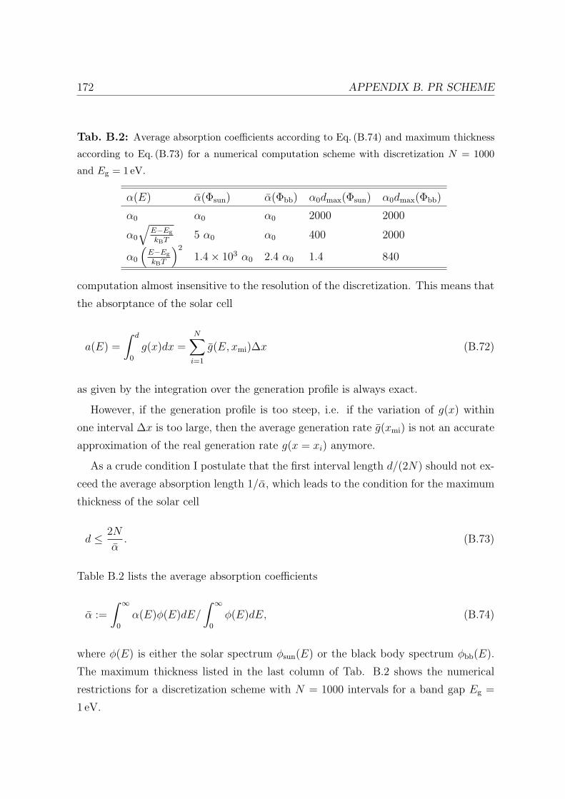
172 APPENDIX B. PR SCHEME
Tab. B.2: Average absorption coefficients according to Eq. (B.74) and maximum thickness
according to Eq. (B.73) for a numerical computation scheme with discretization N = 1000
and Eg = 1 eV.
α(E) α(Φsun) α(Φbb) α0dmax(Φsun) α0dmax(Φbb)
α0 α0 α0 2000 2000
α0
√E−Eg
kBT5 α0 α0 400 2000
α0
(E−Eg
kBT
)2
1.4× 10³ α0 2.4 α0 1.4 840
computation almost insensitive to the resolution of the discretization. This means that
the absorptance of the solar cell
a(E) =
∫ d
0
g(x)dx =N∑
i=1
g(E, xmi)∆x (B.72)
as given by the integration over the generation profile is always exact.
However, if the generation profile is too steep, i.e. if the variation of g(x) within
one interval ∆x is too large, then the average generation rate g(xmi) is not an accurate
approximation of the real generation rate g(x = xi) anymore.
As a crude condition I postulate that the first interval length d/(2N) should not ex-
ceed the average absorption length 1/α, which leads to the condition for the maximum
thickness of the solar cell
d ≤ 2N
α. (B.73)
Table B.2 lists the average absorption coefficients
α :=
∫ ∞
0
α(E)φ(E)dE/
∫ ∞
0
φ(E)dE, (B.74)
where φ(E) is either the solar spectrum φsun(E) or the black body spectrum φbb(E).
The maximum thickness listed in the last column of Tab. B.2 shows the numerical
restrictions for a discretization scheme with N = 1000 intervals for a band gap Eg =
1 eV.
B.7 NUMERICAL ERROR SOURCES 173
B.7.2 Electrical limitations - diffusion length
The electrical current is calculated according to Eq. (3.10) which in the case of the
normalized saturation current and with the discretization scheme of Fig. B.4 becomes
J0
ΦEgbb
= −µnormdν
dξ= −µnorm
ν(ξ = ∆ξ/2)− ν(ξ = 0)
∆ξ/2, (B.75)
where the normalized electron concentration at the junction ν(ξ = 0) = 2 is determined
by the boundary condition Eq. (B.71).
This approximation holds only if the carrier distribution ν(ξ) is not too steep. Let
us assume an exponential decay ν(ξ) ≈ 2exp (−ξ/Lnorm), where Lnorm =√
µnormτnorm
is the normalized diffusion length. Then reducing Lnorm below Lnorm ≈ ∆ξ/2 results
in ν(∆ξ/2) approaching ν(∆ξ/2) = 1. Consequently, the numerical approximation
will be flawed and with ∆ξ = α0d/N the erroneous saturation current approaches the
low-mobility limit
limµnorm→0
J0
ΦEgbb
= −µnormν(ξ = ∆ξ/2)− ν(ξ = 0)
∆ξ/2=
2N
α0dµnorm (B.76)
although in reality, the current follows the square root dependence Jel ∝ √µnormτnorm.
Thus, the numerical discretization scheme is only valid for Lnorm > ∆ξ/2, i.e.
µnorm >(∆ξ)2
4τnorm
=(α0d)2
4N2τnorm
. (B.77)
Summing up, the numerical computations are only valid below a maximum thickness
defined by the average absorption length and above a minimum diffusion length.

Appendix C
Derivation of the two-layer model
This appendix performs the derivation of the two-layer model presented in section
3.7.2.
Region 1: 0 ≤ ξ ≤ ξpr In analogy to Eq. (3.3) without the PR term γint(ξ) we obtain
the following diffusion equation
µnormd2ν
dξ2− ν (ξ) (1 + ϑr)
τ rnorm
= −γsun (ξ)− γbb (ξ)− ϑr
τ rnorm
. (C.1)
For both, plane and textured front surface, I approximate the non-equilibrium gen-
eration profile by the exponential profile
γsun(ξ) =kαF0
ΦEgbb
exp (−kαξ) +kαFr
ΦEgbb
exp (−kα(2α0d− ξ)) (C.2)
in order to guarantee an analytical solution. For the sake of simplicity, I assume that
α(E) = α0 for E ≥ Eg. For a plane front surface, the profile is exact. The amplitudes
F0 and Fr and the path length enhancement factor kα are determined by comparison
with Eq. (B.39). For a textured surface, it holds F0 = JSQsc / (1− tcell(1− tlamb)). I
extract Fr and kα from fitting γsun to the exact generation profile Eq. (B.43). For the
case of a textured front surface and %f = 0 and %b = 1 we obtain for the thicknesses
α0d = 0.1 the coefficients Fr = 1.02 F0 and kα = 3.24, and for the thickness α0d = 10
Fr = 0 and kα = 2. The parameters are chosen in such a way that the integrated
generation profile, i.e. the absorptance of the solar cell does not exceed the actual
absorptance.
174

175
Since I assume that all emitted photons leave the cell, i.e. a constant emission
probability of unity, I also assume a constant black body generation rate γbb(ξ) =
const = 1/τ rnorm. Therewith, we obtain for the excess carriers δν = ν − 1
µnormd2δν
dξ2− δν (ξ)
τnorm
= −kαF0
ΦEgbb
exp (−kαξ)− kαFr
ΦEgbb
exp (−kα(2α0d− ξ)) (C.3)
with the lifetime τnorm = τ rnorm/(ϑr+1). The general solution of this differential equation
reads as
δν1(ξ) = Asinh
(ξ
Lnorm
)+ Bcosh
(ξ
Lnorm
)+ Cexp (−kαξ) + Dexp (kαξ) , (C.4)
where Lnorm =√
µnormτnorm is the normalized diffusion length and the coefficients
C =kαF0τnorm
ΦEgbb (1− k2
αL2norm)
(C.5)
and
D =kαFrexp (−2kαα0d) τnorm
ΦEgbb (1− k2
αL2norm)
(C.6)
are obtained from the particular solutions. The coefficients A and B will follow from
the boundary conditions given below.
Region 2: ξpr ≤ ξ ≤ α0d Deep in the bulk the radiative lifetime is infinity due to the
assumed complete reabsorption of all emitted photons. Along with radiative recombi-
nation the black body generation vanishes as well thereby guaranteeing the compliance
of the internal detailed balance (zero emission is balanced by zero absorption). There-
with we arrive at the following differential equation for the excess carriers:
µnormd2δν
dξ2− δν (ξ)
τnrnorm
= −kαF0
ΦEgbb
exp (−kαξ)kαFr
ΦEgbb
exp (−kα(2α0d− ξ)) , (C.7)
which is identical to Eq. (C.3) in region 1, only that the lifetime is exclusively deter-
mined by the non-radiative lifetime τnrnorm.
With the ansatz
δν2(ξ) = Esinh
(ξ
Lnrnorm
)+ F cosh
(ξ − α0d
Lnrnorm
)+ Gexp (−kαξ) + Hexp (kαξ) , (C.8)

176 APPENDIX C. DERIVATION OF THE TWO-LAYER MODEL
where Lnrnorm =
√µnormτnr
norm is the normalized non-radiative diffusion length, the coef-
ficients G and H read as
G =kαF0τ
nrnorm
ΦEgbb
(1− (kαLnr
norm)2) (C.9)
and
H =kαFrexp (−2kαα0d) τnr
norm
ΦEgbb
(1− (kαLnr
norm)2) . (C.10)
Boundary conditions As boundary conditions we obtain the well-known conditions
δν1(ξ = 0) = exp (qV/(kBT )) − 1 at ξ = 0 and dδν2/dξ|ξ=α0d = 0 at ξ = α0d. At the
Interface between the two regions the continuity of the electron concentration δν(ξ) and
the continuity of the diffusion current result in the conditions δν1(ξ = ξpr) = δν2(ξ =
ξpr) and µnormdδν1/dξ|ξ=ξpr = µnormdδν2/dξ|ξ=ξpr .
Coefficients From these boundary conditions we obtain the coefficients
B = exp
(qV
kBT
)− 1− C −D, (C.11)
E =kαGexp (−kαα0d)−Hexp (kαα0d)
1Lnr
normcosh
(α0d
Lnrnorm
) , (C.12)
F =EK3 −K2sinh
(ξpr
Lnorm
)+ K1
Lnormcosh
(ξpr
Lnorm
)
K4
, (C.13)
and
A =Esinh
(ξpr
Lnrnorm
)+ F cosh
(ξpr−α0d
Lnrnorm
)+ K1
sinh(
ξpr
Lnorm
) , (C.14)
where the abbreviations K1, K2, K3, and K4 are given by
K1 = (G− C) exp (−kαξpr) + (H −D) exp (kαξpr)−Bcosh
(ξpr
Lnorm
), (C.15)
K2 = kα (C −G) exp (−kαξpr)+kα (H −D) exp (kαξpr)− B
Lnorm
sinh
(ξpr
Lnorm
), (C.16)
K3 =1
Lnorm
cosh
(ξpr
Lnorm
)sinh
(ξpr
Lnrnorm
)− 1
Lnrnorm
sinh
(ξpr
Lnorm
)cosh
(ξpr
Lnrnorm
),
177
(C.17)
and
K4 =1
Lnrnorm
sinh
(ξpr
Lnorm
)sinh
(ξpr − α0d
Lnrnorm
)−
1
Lnorm
cosh
(ξpr
Lnorm
)cosh
(ξpr − α0d
Lnrnorm
). (C.18)
Layer thickness In order to comply the external detailed balance principle, we have
to guarantee that the radiative recombination current does not exceed the absorptance
a of the solar cell. Therefore, I choose the thickness ξpr of layer 1 in such a way,
that the maximum radiative recombination current J rad0 (µnorm → ∞)/ΦEg
bb equals the
absorptance and therewith the numerical result in section 3.4.1.
Radiative recombination only takes place in region 1. Therefore, and with keeping
in mind that all photons emitted by radiative recombination are also emitted from the
front surface by definition (no PR), we obtain the radiative saturation current
J rad0
ΦEgbb
=
∫ ξpr
0
δν1
τ rnorm
dξ
∣∣∣∣∣V =kBT/qln(2)
. (C.19)
For µnorm → ∞ and with δν1(ξ = 0) = 1 for V = (kBT/q)ln (2) it holds δν1(ξ) =
δν1(ξ = 0) = 1. Therewith, we arrive at the condition
limµnorm→∞
J rad0
ΦEgbb
=ξpr
τ rnorm
!= a (C.20)
which with τ rnorm = 1/(4n2) gives
ξpr =a
4n2. (C.21)
The absorptance a is either given by Eq. (3.37) for a textured or Eq. (3.40) for a plane
front surface.
With the above choice of the layer thickness ξpr, the model inherently predicts the
correct high mobility limit for the saturation current in the radiative recombination
limit. When non-radiative recombination is dominant, the model simply turns into the
classical approach.
With respect to the low mobility limit the model also renders the correct result,
namely the limit√
µnorm/τ rnorm. But this limit is not the crucial point since it is
178 APPENDIX C. DERIVATION OF THE TWO-LAYER MODEL
also correctly reproduced by the standard classical model. The high mobility limit
makes up the much more critical issue, since the change from the limit α0d/τnrnorm to
the absorptance a with increasing non-radiative lifetime can not be captured with the
classical approach.
The final step in the model is the calculation of the electrical current which is
conducted in the usual manner according to
Jel(V )
ΦEgbb
= µnormdδν1
dξ
∣∣∣∣∣ξ=0
= µnorm
(A
Lnorm
− kαC + kαD
). (C.22)
C.0.2.1 Radiative recombination limit
In the limit of radiative recombination, the two-layer model allows some simplifications.
Without non-radiative recombination, i.e. with an infinite non-radiative lifetime, the
lifetime in region 1 is simply given by the radiative lifetime and the diffusion length
turns into Lnorm =√
µnormτ rnorm. In region 2, recombination vanishes altogether. With-
out the recombination term δν2/τnrnorm in Eq. (C.7), the electron profile in region 2 is
given by
δν2(ξ) = Eξ + F + Gexp (−kαξ) + Hexp (kαξ) (C.23)
with the coefficients
G =−F0
ΦEgbbk2
αµnorm
, (C.24)
H =Frexp (−2kαα0d)
ΦEgbbk2
αµnorm
, (C.25)
and
E = kαGexp (−kαα0d)− kαHexp (kαα0d) . (C.26)
From the boundary conditions at ξ = ξpr we obtain
A =(E + K2)Lnorm
cosh(
ξpr
Lnorm
) (C.27)
and
F = Asinh
(ξpr
Lnorm
)− Eξpr −K1. (C.28)
The coefficients B, C, D, and K1 and K2 remain unchanged.

Nomenclature
Physical constants
c Speed of light 3× 1010 cm s−1
h Planck’s constant 4.14× 10⁻¹⁵ eV s
kB Boltzmann’s constant 8.62× 10⁻⁵ eV K−1
q Elementary charge 1.602× 10⁻¹⁹ As
Symbols
aloc Local absorptance
αloc Local absorption coefficient cm−1
αsun Average absorption coefficient of the solar spectrum cm−1
asun Average absorptance of the solar spectrum
abb Average absorptance of the terrestrial black body spec-
trum
Beven Reflected path coming from the back side with even #
of reflections
Bodd Reflected path coming from the back side with odd #
of reflections
cµ Proportionality constant between the normalized short
circuit current in the low mobility limit and the normal-
ized mobility
cr Radiative lifetime multiplication factor
dcrit Critical thickness for light absorption cm
dim Dimension of band gap fluctuations
179
180 NOMENCLATURE
dmax Maximum thickness for numerical accuracy cm
Dn Electron diffusion constant cm2 s−1
EC Conduction band eV
ElocC Local conduction band eV
EF Fermi level eV
EFn Electron Fermi level eV
ElocFn Local electron Fermi level eV
EFp Hole Fermi level eV
ElocFp Local hole Fermi level eV
Eg Band gap eV
Elocg Local band gap eV
EV Valence band eV
ElocV Local valence band eV
Eg Mean band gap eV
EQE External quantum efficiency (spectral)
EQELED External LED quantum efficiency (integrated)
η Solar cell power conversion efficiency
ηSQ Shockley Queisser efficiency
fC Collection efficiency
FF Fill factor
F0 Initial photon flux at the solar cell surface cm−2 s−1
Fr Reflected photon flux cm−2 s−1
Feven Reflected path coming from the front side with an even
# of reflections
Fodd Reflected path coming from the front side with an odd
# of reflections
fr Radiative interaction function
φdΩbb,n Spectral black body photon flux per solid angle in a
material with refractive index n
cm−2 s−1 eV−1
φbb Spectral black body photon flux projected on the cell
surface
cm−2 s−1 eV−1
Φbb Integrated black body photon flux projected on the cell
surface
cm−2 s−1
NOMENCLATURE 181
ΦEgbb Black body photon flux integrated from the band gap
and projected on the cell surface
cm−2 s−1
Φabsbb Integrated black body photon flux absorbed by the cell cm−2 s−1
φsun Spectral solar photon flux projected on the cell surface cm−2 s−1 eV−1
Φsun Solar photon flux integrated over all energies and pro-
jected on the cell surface
cm−2 s−1
ΦEgsun Solar photon flux integrated over all energies larger than
the band gap and projected on the cell surface
cm−2 s−1
Φabssun Integrated solar photon flux absorbed by the cell per
unit surface area
cm−2 s−1
Φlocr Local radiative recombination current cm−2 s−1
Φem Integrated emitted photon flux per unit surface area cm−2 s−1
gbb Spectral black body generation rate cm−3 s−1 eV−1
Gbb Black body generation rate cm−3 s−1
γbb Normalized black body generation rate
gint Spectral internal generation rate cm−3 s−1 eV−1
Gint Internal generation rate cm−3 s−1
γint Normalized internal generation rate
gsun Spectral solar generation rate cm−3 s−1 eV−1
Gsun Solar generation rate cm−3 s−1
γsun Normalized solar generation rate
Jel Electrical current drawn from the solar cell cm−2 s−1
J0 Reverse saturation current cm−2 s−1
JSQ0 Saturation current in the SQ limit cm−2 s−1
J rad0 Radiative saturation current cm−2 s−1
Jnr0 Non-radiative saturation current cm−2 s−1
J locnr Local non-radiative recombination current cm−2 s−1
J locrec Local recombination current cm−2 s−1
Jnrrec Non-radiative recombination current cm−2 s−1
J radrec Radiative recombination current cm−2 s−1
Jsc Short circuit current cm−2 s−1
JSQsc Short circuit current in the SQ limit cm−2 s−1

182 NOMENCLATURE
kα Absorption multiplication factor that contains the ab-
sorption spectrum and the nature of the cell surface
klam Absorption multiplication factor that contains the na-
ture of the cell surface
Lα Absorption length cm
Lα,norm Normalized absorption length
Ln Electron diffusion length cm
Lnorm Normalized diffusion length
Lcrit Critical diffusion length cm
Lradcrit Critical diffusion length in the radiative limit cm
Lem,norm Normalized emission length
Lg Fluctuation length of band gap fluctuations cm
Lg Fluctuation length of the chemical potential cm
µ Chemical potential of photons eV
µloc Local chemical potential eV
µss Steady state chemical potential eV
µlocss Local steady state chemical potential eV
µ Mean chemical potential eV
µn Electron mobility cm2( Vs)−1
µref Reference mobility for normalization cm2( V s)−1
µnorm Normalized mobility
µcrit Critical mobility cm2( Vs)−1
µnormcrit Normalized critical mobility
µradcrit Critical mobility in the radiative recombination limit cm2( Vs)−1
µbandp Hole mobility in valence band cm2( V s)−1
µeffp Effective hole mobility cm2( V s)−1
NA Acceptor concentration cm−3
ni Intrinsic carrier concentration cm−3
n Electron concentration cm−3
ν Normalized electron concentration
n Real part of the refractive index
p Hole concentration cm−3
PG Gaussian probability

NOMENCLATURE 183
%b Reflection coefficient at the back contact
%f Reflection coefficient at the front surface
rr Spectral radiative recombination rate cm−3 s−1 eV−1
Rr Radiative recombination rate cm−3 s−1
Rnr Non-radiative recombination rate cm−3 s−1
Rg Autocorrelation function of the band gap fluctuations
Sg Power spectrum of the band gap fluctuations cmdim
σg Standard devieation of the band gap fluctuations eV−1
σµ Standard devieation of the chemical potential eV−1
Sn Electron surface recombination velocity at the back con-
tact
cm s−1
τ Minority carrier lifetime s−1
τnorm Normalized lifetime
τr Radiative minority carrier lifetime s−1
τ rnorm Normalized radiative minority carrier lifetime
τnr Non-radiative minority carrier lifetime s−1
τnrnorm Normalized non-radiative minority carrier lifetime
τmodnorm Normalized modified minority carrier lifetime
τ r,modnorm Normalized modified radiative minority carrier lifetime
θc Critical angle of total internal reflection
ϑr Ratio of radiative and non-radiative lifetime
Voc Open circuit voltage V
V inhomoc Open circuit voltage with inhomogeneous band gap V
V radoc Open circuit voltage in the Shockley Queisser limit V
wscr Width of the space charge region cm
x Spatial coordinate cm
ξ Normalized spatial coordinate
xg Position of carrier generation cm
xi Discrete position (interval) of carrier generation cm
xr Position of carrier recombination cm
xj Discrete position (interval) of carrier recombination cm
ξpr Normalized depth of the layer from where all emitted
photons exit the cell

Bibliography
[1] H. Queisser, Kristalline Krisen (Piper, Munche, 1985).
[2] A. Shah, P. Torres, R. Tscharner, N. Wyrsch, and H. Keppner,
Science 285, 692 (1999).
[3] A. Goetzberger, C. Hebling, and H.-W. Schock, Mat. Sc. Eng. R 40, 1
(2003).
[4] K. L. Chopra, P. D. Paulson, and V. Dutta, Prog. Photovolt. 12, 69
(2004).
[5] E. A. Schiff, Sol. En. Mat. Sol. Cells 78, 567 (2003).
[6] U. Rau and H.-W. Schock, Appl. Phys. A 69, 131 (1999).
[7] S. E. Shaheen, D. S. Ginley, and G. E. Jabbour, MRS Bulletin 30, 10
(2005).
[8] M. Graetzel, MRS Bulletin 30, 23 (2005).
[9] M. A. Green, Physica E 14, 65 (2002).
[10] W. Shockley and H. J. Queisser, J. Appl. Phys. 32, 510 (1961).
[11] W. Shockley, Bell Syst. Tech. J. 28, 435 (1949).
[12] M. A. Green, Solar cells: operating principles, technology, and system applica-
tions (Englewood Cliffs : Prentice-Hall, 1982).
[13] R. Hulstrom, R. Bird, and C. Riordan, Sol. Cells 15, 365 (1985).
184

BIBLIOGRAPHY 185
[14] T. Tiedje, E. Yablonovitch, G. Cody, and B. Brooks, IEEE Trans. on
Electr. Devices ED-31, 711 (1984).
[15] P. Wurfel, J. Phys. C 15, 3967 (1982).
[16] U. Rau, Phys. Rev. B 76, 085303 (2007).
[17] S. Sze, Semiconductor devices: physics and technology (Wiley, 2002).
[18] N. Arora, S. G. Chamberlain, and D. J. Roulston, Appl. Phys. Lett.
37, 325 (1980).
[19] W. P. Dumke, Phys. Rev. 105, 139 (1957).
[20] T. S. Moss, Proc. Phys. Soc. B 70, 247 (1957).
[21] P. T. Landsberg, Proc. Phys. Soc. B 70, 1175 (1957).
[22] W. N. Carr, Infrared Phys. 6, 1 (1966).
[23] S. Kameda and W. N. Carr, J. Appl. Phys. 44, 2910 (1973).
[24] C. J. Hwang, Phys. Rev. B. 6, 1355 (1972).
[25] F. Stern and J. M. Woodall, J. Appl. Phys. 45, 3904 (1974).
[26] T. Kuriyama, T. Kamiya, and H. Yanai, Jpn. J. Appl Phys. 16, 465 (1977).
[27] H. C. Casey Jr., B. I. Miller, and E. Pinkas, J. Appl. Phys. 44, 1281
(1973).
[28] P. Asbeck, J. Appl. Phys. 48, 820 (1977).
[29] K. Mettler, Phys. Stat. Sol. (a) 49, 163 (1978).
[30] R. J. Roedel and V. G. Keramidas, J. Appl. Phys. 50, 6353 (1979).
[31] W. Ruhle, L. Hoffmann, and S. Leibenzeder, J. Appl. Phys. 53, 3765
(1982).
[32] V. V. Rossin and V. G. Sidorov, Sov. Phys. Semicond. 15, 106 (1981).

186 BIBLIOGRAPHY
[33] V. V. Rossin and V. G. Sidorov, Sov. Phys. Semicond. 18, 702 (1984).
[34] T. Kamiya, s. Hirose, and H. Yanai, J. Luminescence 18/19, 910 (1979).
[35] B. Bensaıd, F. Raymond, C. Leroux, M. and Verie, and B. Fofana,
J. Appl. Phys. 66, 5542 (1989).
[36] V. I. Korol’kov, E. P. Romanova, V. S. Yuferev, and A. A.
Yakovenko, Sov. Phys. Semicond. 14, 1005 (1980).
[37] E. Velmre, B. Freidin, and A. Udal, Physica Scripta 24, 468 (1981).
[38] J. W. Parks Jr. and K. F. Brennan, J. Appl. Phys. 82, 3493 (1997).
[39] P. Enders, Phys. Stat. Sol. (b) 137, 353 (1986).
[40] O. v. Roos, J. Appl. Phys. 54, 2495 (1983).
[41] P. Enders, Phys. Stat. Sol. (b) 137, 701 (1986).
[42] P. Enders, Phys. Stat. Sol. (b) 141, 317 (1987).
[43] V. V. Rossin, A. L. Vinke, and V. G. Sidorov, Sov. Phys. Semicond. 13,
647 (1979).
[44] Lastras-Martınez, J. Appl. Phys. 50, 4156 (1979).
[45] V. V. Rossin and V. G. Sidorov, Sov. Phys. Semicond. 14, 1167 (1980).
[46] O. v. Roos, J. Appl. Phys. 54, 1390 (1983).
[47] O. v. Roos, Sol.-State El. 27, 913 (1984).
[48] V. S. Yuferev and M. P. Proskura, Sov. Phys. Semicond. 18, 530 (1984).
[49] P. Renaud, F. Raymond, B. Bensaid, and C. Verie, J. Appl. Phys. 71,
1907 (1992).
[50] V. Badescu and P. Landsberg, Semicond. Sci. Technol. 8, 1267 (1993).
[51] J. E. Parrott and A. Potts, in Proc. 22nd IEEE Photovoltaics Specialist
Conf. (1991), p. 153.

BIBLIOGRAPHY 187
[52] S. M. Durbin and J. L. Gray, in Proc. 22nd IEEE Photovoltaics Specialist
Conf. (1991), p. 188.
[53] S. M. Durbin and J. L. Gray, IEEE Trans. on Electr. Devices 41, 239 (1994).
[54] V. Badescu and P. Landsberg, Semicond. Sci. Technol. 12, 1491 (1997).
[55] A. Yamamoto, M. Kurizuka, M. M. Murshid, M. Ohkubo, and
A. Hashimoto, Sol. En. Mat. Sol. Cells 50, 259 (1998).
[56] J. L. Balenzategui and A. Martı, Sol. En. Mat. Sol. Cells 90, 1068 (2006).
[57] J. E. Parrott, Sol. En. Mat. Sol. Cells 30, 221 (1993).
[58] R. J. Nelson and R. G. Sobers, J. Appl. Phys. 49, 6103 (1978).
[59] S. D. Lester, T. S. Kim, and B. G. Streetman, Appl. Phys. Lett. 52, 476
(1988).
[60] R. K. Ahrenkiel, D. J. Dunlavy, and T. Hanak, J. Appl. Phys. 64, 1916
(1988).
[61] R. K. Ahrenkiel, D. J. Dunlavy, and B. M. Keyes, Appl. Phys. Lett.
55, 1088 (1989).
[62] R. K. Ahrenkiel, B. M. Keyes, G. B. Lush, M. R. Melloch, M. S.
Lundstrom, and H. F. MacMillan, J. Vac. Sci. Technol. A 10, 990 (1992).
[63] G. B. Lush, H. F. MacMillan, B. M. Keyes, D. H. Levi, M. R. Mel-
loch, R. K. Ahrenkiel, and M. S. Lundstrom, J. Appl. Phys. 72, 1436
(1992).
[64] M. J. Kerr, A. Cuevas, and P. Campbell, Prog. Photovolt: Res. Appl. 11,
97 (2003).
[65] E. P. Romanova and V. S. Yuferev, Sov. Phys. Semicond. 14, 1430 (1980).
[66] V. V. Rossin and V. G. Sidorov, Sov. Phys. Semicond. 15, 1056 (1981).
[67] C. Donolato, Appl. Phys. Lett. 46, 270 (1984).

188 BIBLIOGRAPHY
[68] J. I. Pankove, Optical Processes in Semiconductors (Prentice-Hall, Inc., En-
glewood Cliffs, N.J., 1971).
[69] R. Brendel and H. J. Queisser, Sol. Energy Mat. Sol. Cells 29, 397 (1993).
[70] G. L. Araujo and A. Martı, Sol. En. Mat. Sol. Cells 33, 213 (1994).
[71] L. Ley, in The Physics of Hydrogenated Amorphous Silicon II, edited by J. D.
Joannopopoulos and G. Lucovsky (Springer Verlag, Heidelberg, 1984).
[72] K. Orgassa, Coherent optical analysis of the ZnO/CdS/Cu(In,Ga)Se2 thin film
solar cell, Phd thesis, University of Stuttgart (2004).
[73] T. Trupke, M. A. Green, P. Wurfel, P. Altermatt, A. Wang,
J. Zhao, and R. Courkish, J. Appl. Phys. 94, 4930 (2003).
[74] K. Puech, S. Zott, K. Leo, M. Ruckh, and H.-W. Schock, Appl. Phys.
Lett. 69, 3375 (1996).
[75] P. J. Rostan, U. Rau, V. X. Nguyen, T. Kirchartz, M. B. Schubert,
and J. H. Werner, Sol. En. Mat. Sol. Cells 90, 1345 (2006).
[76] M. J. Kerr and A. Cuevas, J. Appl. Phys. 91, 2473 (2002).
[77] M. A. Green, IEEE Trans. on Electron Devices ED-31, 671 (1984).
[78] J. Zhao, A. Wang, M. A. Green, and F. Ferrazza, Appl. Phys. Lett. 73,
1991 (1998).
[79] M. Taguchi, H. Sakata, Y. Yoshimine, E. Maruyama, A. Terakawa,
M. Tanaka, and S. Kiyama, in Proc. 31st IEEE Photovolt. Spec. Conf. (IEEE,
New York, 2005), p. 866.
[80] J. Meier, J. Sitznagel, U. Kroll, C. Bucher, S. Fay, T. Moriarty,
and A. Shah, Thin Solid Films 451, 518 (2004).
[81] E. A. Schiff, R. I. Devlen, H. T. Grahn, and J. Tauc, Appl. Phys. Lett.
54, 1911 (1989).

BIBLIOGRAPHY 189
[82] G. Juska, K. Arlauskas, J. Kocka, M. Hoheisel, and P. Chabloz,
Phys. Rev. Lett. 75, 2984 (1995).
[83] E. A. Schiff, J. Non-Cryst. Sol. 352, 1087 (2006).
[84] Q. Gu, Q. Wang, E. A. Schiff, Y.-M. Li, and C. T. Malone, J. Appl.
Phys. 76, 2310 (1994).
[85] J. Lee, J. D. Cohen, and W. N. Shafarman, Thin Solid Films 480, 336
(2005).
[86] J. H. Werner, J. Mattheis, and U. Rau, Thin Solid Films 480, 399 (2005).
[87] B. Ohnesorge, R. Weigand, G. Bacher, and A. Forchel, Appl. Phys.
Lett. 73, 1224 (1998).
[88] J. Mattheis, P. J. Rostan, K. Orgassa, U. Rau, and J. H. Werner,
Sol. En. Mat. Sol. Cells .
[89] K. Ramanathan, M. A. Contreras, C. L. Perkins, S. Asher, F. S.
Hasoon, J. Keane, D. Young, M. Romero, W. Metzger, R. Noufi,
J. Ward, and A. Duda, Prog. Photovolt: Res. Appl. 11, 225 (2003).
[90] T. Kirchartz, U. Rau, J. Mattheis, and J. H. Werner, unpublished
(2007).
[91] M. Topic, F. Smole, and J. Furlan, J. Appl. Phys. 79, 8537 (1996).
[92] B. A. Gregg, J. Phys. Chem. B 107, 4688 (2003).
[93] B. A. Gregg and M. C. Hanna, J. Appl. Phys. 93, 3605 (2003).
[94] H. Hoppe and N. S. Sariciftci, J. Mat. Res. 19, 1924 (2004).
[95] S. E. Gledhill, B. Scott, and B. A. Gregg, J. Mat. Res. 20, 3167 (2005).
[96] N. K. Patel, S. Cina, and J. H. Burroughes, IEEE J. Sel. Topics Quantum
El. 8, 346 (2002).
[97] J. H. Werner and H. H. Guttler, J. Appl. Phys. 69, 1522 (1991).

190 BIBLIOGRAPHY
[98] U. Rau and J. H. Werner, Appl. Phys. Lett. 84, 3735 (2004).
[99] D. Eich, U. Herber, U. Groh, U. Stahl, C. Heske, M. Marsi, M. Kiski-
nova, W. Riedl, R. Fink, and E. Umbach, Thin Solid Films 361-362, 258
(2000).
[100] Y. Yan, R. Noufi, K. M. Jones, K. Ramanathan, and M. M. Al-Jassim,
Appl. Phys. Lett. 87, 121904 (2005).
[101] V. G. Karpov, A. D. Compaan, and D. Shvydka, Appl. Phys. Lett. 80,
4256 (2002).
[102] V. G. Karpov, A. D. Compaan, and D. Shvydka, Phys. Rev. B 69, 1
(2004).
[103] P. O. Grabitz, U. Rau, and J. H. Werner, Phys. Stat. Sol. (a) 202, 2920
(2005).
[104] P. A. Fedders, D. A. Drabold, and S. Nakhmanson, Phys. Rev. B 58,
15624 (1998).
[105] F. Urbach, Phys. Rev. 92, 1324 (1953).
[106] T. Skettrup, Phys. Rev. B 18, 2622 (1978).
[107] D. J. Dunstan, J. Phys. C 30, L419 (1982).
[108] M. Roberts and D. J. Dunstan, J. Phys. C 18, 5429 (1985).
[109] J. Osvald, J. Appl. Phys. 85, 1935 (1999).
[110] M. Schofthaler, U. Rau, and J. H. Werner, J. Appl. Phys. 76, 4168
(1994).
[111] A. Papoulis, Probability, Random Variables, and Stochastic Processes
(McGraw-Hill, Inc, 1991).
[112] M. A. Green, J. Appl. Phys. 81, 268 (1997).
[113] S. Dauwe, Low-Temperature Surface Passivation of crystalline Silicon, Phd the-
sis, Universitat Hannover (2004).

BIBLIOGRAPHY 191
[114] S. J. Orfanidis, Optimum signal processing: An introduction (MacMillan Pub-
lishing Company, New York, 1985).
[115] A. Gabor, J. Tuttle, D. S. Albin, M. Contreras, R. Noufi, and
A. Hermann, Appl. Phys. Lett. 65, 198 (1994).
[116] K. Bothe, G. H. Bauer, and T. Unold, Thin Solid Films 403, 453 (2002).
[117] B. Dimmler, H. Dittrich, and H.-W. Schock, in Conf. Rec. 19th IEEE
Photov. Spec. Conf. (IEEE, New York, 1987), p. 1454.
[118] I. Dirnstorfer, M. T. Wagner, D. M. Hofmann, M. D. Lampert,
F. Karg, and B. K. Meyer, Phys. Stat. Sol. (a) 168, 163 (1998).
[119] A. Bauknecht, S. Siebentritt, J. Albert, and M. C. Lux-Steiner, J.
Appl. Phys. 89, 4391 (2001).
[120] N. Rega, S. Siebentritt, I. E. Beckers, J. Beckmann, J. Albert, and
M. C. Lux-Steiner, Thin Solid Films 431, 186 (2003).
[121] N. Rega, S. Siebentritt, J. Albert, S. Nishiwaki, A. Zajoqin, M. C.
Lux-Steiner, R. Kniese, and M. J. Romero, Thin Solid Films 480, 286
(2005).
[122] T. Kirchartz, U. Rau, M. Kurth, J. Mattheis, and J. H. Werner,
Thin Solid Films 515, 6238 (2007).
[123] T. Kirchartz and Rau, J. Appl. Phys. 102, 104510 (2007).
[124] E. Daub and P. Wurfel, Phys. Rev. Lett. 74, 1020 (1995).
[125] T. Trupke, E. Daub, and P. Wurfel, Sol. En. Mat. Sol. Cells 53, 103
(1998).
[126] T. Unold, D. Berkhahn, B. Dimmler, and G. H. Bauer, in Proc. 16th
Europ. Photovolt. Sol. Energy Conf., Glasgow, edited by H. Scheer, B. Mc-
Nellis, W. Palz, H. A. Ossenbrink, and P. Helm (James & James Ltd,
London, 2000), p. 736.
[127] M. Turcu, I. M. Kotschau, and U. Rau, J. Appl. Phys. 91, 1391 (2002).

192 BIBLIOGRAPHY
[128] W. N. Shafarman, R. Klenk, and B. E. McCandless, J. Appl. Phys. 79,
7327 (1996).
[129] J. T. Heath, J. D. Cohen, W. N. Shafarman, D. X. Liao, and A. A.
Rockett, Appl. Phys. Lett. 80, 4540 (2002).
[130] T. Schlenker, J. Mattheis, M. Bogicevic, U. Rau, and J. H. Werner,
in Proc. 20th Eur. Photovolt. Solar Energy Conf., edited by W. Palz, H. Os-
senbrink, and P. Helm (WIP-Renewable Energies, Munchen, 2005), p. 1775.
[131] L. Gutay and G. H. Bauer, Thin Solid Films 487, 8 (2005).
[132] P. O. Grabitz, U. Rau, B. Wille, G. Bilger, and J. H. Werner, J.
Appl. Phys. 100, 124501 (2006).
[133] P. O. Grabitz, Phd thesis, University of Stuttgart (2007).
[134] P. O. Grabitz, U. Rau, and J. H. Werner, Thin Solid Films 487, 14
(2005).
[135] O. S. Heavens, Optical Properties of Thin Solid Films (Butterworths, London,
1955).
[136] T. Dullweber, U. Rau, M. A. Contreras, R. Noufi, and H.-W.
Schock, IEEE Trans. Electr. Devices 47, 2249 (2000).
[137] T. Dullweber, O. Lundberg, J. Malmstrom, M. Bodegard, L. Stolt,
U. Rau, H.-W. Schock, and J. H. Werner, Thin Solid Films 387, 11
(2001).
[138] S. Siebentritt, Thin Solid Films 403, 1 (2002).
[139] M. Turcu, O. Pakma, and U. Rau, Appl. Phys. Lett. 80, 2598 (2002).
[140] U. Rau, in Proc. 3rd World Conf. Photovolt. Energy Conv., Osaka, edited
by K. Kurosawa, L. L. Kazmerski, B. McNellis, M. Yamaguchi,
C. Wronski, and W. C. Sinke (2003), p. 2847.
[141] R. Kniese, D. Hariskos, G. Voorwinden, U. Rau, and M. Powalla,
Thin Solid Films 431, 543 (2003).

BIBLIOGRAPHY 193
[142] S. Siebentritt and U. Rau (Eds.), Wide-Gap Chalcopyrites (Springer Series
in Materials Science 86, Springer, Berlin, Heidelberg, Germany, 2006).
[143] G. Hanna, A. Jasenek, U. Rau, and H.-W. Schock, Thin Solid Films
387, 71 (2001).
[144] M. A. Green, E.-C. Cho, Y. Cho, Y. Huang, E. Pink, T. Trupke,
A. Lin, T. Fangsuwannarak, T. Puzzer, G. Conibeer, and R. Cork-
ish, in Proc. 20th Eur. Photovolt. Solar Energy Conf., edited by W. Palz,
H. Ossenbrink, and P. Helm (WIP-Renewable Energies, Munchen, 2005),
p. 3.
[145] A. Luque and A. Martı, Phys. Rev. Lett. 78, 5014 (1997).
[146] U. Rau and R. Brendel, J. Appl. Phys. 84, 6412 (1998).
[147] D. Werner, Funktionalanalysis (Springer Verlag Berlin, 2002).
[148] W. v. Roosbroeck and W. Shockley, Phys. Rev. 94, 1558 (1954).
[149] E. Yablonovitch, J. Opt. Soc. Am. 72, 899 (1982).
[150] M. A. Green, Prog. Photovolt: Res.Appl. 10, 235 (2002).
[151] C. Großmann and H.-G. Roos, Numerik partieller Differentialgleichungen
(Teubner Verlag Stuttgart, 1994).

Curriculum Vitae
Personliche Angaben
Name Julian Mattheis
Geburtsdatum 14.12.1975
Geburtsort Hannover
Schulbildung und Zivildienst
07/1995 Allgemeine Hochschulreife am Grotefend Gymnasium
Munden
Abiturnote: 1,4
08/1995-07/1996 Zivildienst in einem Kindergarten des Roten Kreuzes fur
geistig und korperlich behinderte Kinder
Studium und Promotion
10/1996-07/2002 Studium der Elektrotechnik an der Technischen Univer-
sitat Braunschweig und der Universitat Stuttgart
Diplomnote: Sehr Gut
10/2002-04/2006 Studium der Politikwissenschaft mit Nebenfachern
Volkswirtschaftslehre und Mathematik
Magisternote: Gut
09/2002-10/2006 Wissenschaftlicher Mitarbeiter am Institut fur
Physikalische Elektronik, Universitat Stuttgart
Berufliche Tatigkeit
seit 11/2006 Mitarbeiter im Produktmanagement und in Forschung
& Entwicklung, Q-Cells AG
194

List of Publications
(1) J. Mattheis, J. H. Werner, and U. Rau, Finite mobility effects on the radiative
efficiency limit of pn-junction solar cells, Phys. Rev. B, in print
(2) J. Mattheis, U. Rau, and J. H. Werner, Light absorption and emission in semi-
conductors with band gap fluctuations - a study on Cu(In,Ga)Se2 thin films, J.
Appl. Phys. 101, 113519 (2007)
(3) J. Mattheis, P. J. Rostan, K. Orgassa, U. Rau, and J. H. Werner, Carrier collec-
tion in Cu(In,Ga)Se2 solar cells with graded band gaps and transparent ZnO:Al
back contacts, Solar Energy Materials and Solar Cells 91, 689 (2007)
(4) T. Kirchartz, U. Rau, M. Kurth, J. Mattheis and J.H. Werner, Comparative
study of electroluminescence from Cu(In,Ga)Se2 and Si solar cells, Thin Solid
Films 515, 6238 (2007)
(5) Philip Jackson, Roland Wurz, Matthias Kurth, Julian Mattheis,Thomas Schlotzer,
Kay Orgassa, Uwe Rau, Gerhard Bilger, and Jurgen H. Werner, High Quality
Baseline for High Efficiency Cu(In1−x,Gax)Se2 Solar Cells, Prog. Photovolt.
15, 507 (2007)
(6) A. Halverson, J. Mattheis, U. Rau, and J. D. Cohen, Reverse bias induced
metastable effects in Cu(In,Ga)Se2 photovoltaic devices in Proc. 4th World Con-
ference on Photovoltaic Energy Conversion, edited by: (IEEE, New York, USA,
2006), 519 - 522 (2006)
(7) J. Mattheis, U. Rau, and J. H. Werner, Finite mobility effects on the radiative
efficiency limit of pn-junction solar cells in Proc. 4th World Conference on
Photovoltaic Energy Conversion, edited by: (IEEE, New York, USA, 2006), 95 -
98 (2006)
195

196 LIST OF PUBLICATIONS
(8) J. H. Werner, J. Mattheis, and U. Rau, Efficiency limitations of polycrystalline
thin film solar cells: case of Cu(In,Ga)Se2, Thin Solid Films 480-481, 399 - 409
(2005)
(9) P. J. Rostan, J. Mattheis, G. Bilger, U. Rau, and J. H. Werner, Formation of
transparent and ohmic ZnO:Al/MoSe2 contacts for bifacial Cu(In,Ga)Se2 solar
cells and tandem structures, Thin Solid Films 480-481, 67 - 70 (2005)
(10) J. Mattheis, T. Schlenker, M. Bogicevic, U. Rau, and J. H. Werner, Band gap
fluctuations in Cu(In,Ga)Se2 thin films, Mat. Res. Soc. Symp. Proc. 865,
F16.4.1, San Francisco (2005)
(11) H.-D. Mohring, U. Heckmann, J. Mattheis, and U. Rau, High efficiency CIS
modules for PV concentrator systems, in Proc. 20th European Photovoltaic Solar
Energy Conference, 1796 - 1799, Barcelona (2005)
(12) T. Schlenker, J. Mattheis, M. Bogicevic, U. Rau, and J. H. Werner, Optical anal-
ysis of band gap inhomogeneities in CuInSe2 thin films, in Proc. 20th European
Photovoltaic Solar Energy Conference, 1775 - 1778, Barcelona (2005)
(13) J. Mattheis, P. J. Rostan, U. Rau, and J. H. Werner, Carrier collection in
Cu(In,Ga)Se2 solar cells with transparent ZnO:Al back contacts, in Technical Di-
gest of the 14th international Photovoltaic Science and Engineering Conference,
Bangkok (2004)
(14) G. Hanna, J. Mattheis, V. Laptev, Y. Yamamoto, U. Rau, and H. W. Schock,
Influence of the selenium flux on the growth of Cu(In,Ga)Se2 thin films, Thin
Solid Films 431-432, 31 - 36 (2003)
(15) U. Rau, V. X. Nguyen, J. Mattheis, M. Rakhlin, and J. H. Werner, Recombination
at a-Si:H/c-Si heterointerfaces and in a-Si:H/c-Si heterojunction solar cells, in
Proc. 3rd World Conf. Potovolt. Energy Conv., Osaka (2003)

Danksagung
Mein Dank gilt ganz besonders meinem Doktorvater Prof. Jurgen H. Werner, der mit
seiner Mischung aus Forderungen und Lob genau den richtigen Ton getroffen hat, um
mich maximal zu motivieren. Ihm verdanke ich viele grundlegende Einsichten in Bezug
auf die Berechnung maximaler Wirkungsgrade und in Bezug auf die Modellierung von
Bandluckenfluktuationen. Ohne ihn ware diese Arbeit gar nicht ins Rollen gekommen.
Ich ware gar nicht auf die Idee gekommen, uber Inhomogenitaten nachzudenken. Bei
allen meinen Wunschen - sei es flexible Arbeitseinteilung fur mein Zweitstudium oder
die finanzielle Unterstutzung eines Auslandsaufenthaltes - habe ich stets seine vollste
Unterstutzung bekommen.
Ein bombastisches Riesen-Dankeschon an meinen Gruppenleiter Dr. habil. Uwe
Rau. Dieser geniale Kopf und Inbegriff des zerstreuten Physikers hat einen ganz er-
heblichen Anteil an samtlichen Modellen in dieser Arbeit. Ich war ziemlich stolz, dass
es ihn immerhin fast eine ganze Woche gekostet hat, das Photon Recycling Modell in
Matlab zu programmieren, fur das ich ein ganzes Jahr gebraucht habe. Denn unter
Umstanden kann es durchaus vorkommen, dass er an einem Nachmittag macht, wofur
normale Menschen die vollen drei Jahre ihrer Promotion benotigen.
Vielen Dank auch an
• Martin Wagner fur die Prozessierung von Proben,
• Martin Bogicevic fur Absorptionsmessungen,
• Saioa Tardon von der Universitat Oldenburg fur Photolumineszenzmessungen,
• Thomas Gustav Schlenker und Peter Grabitz fur intensive Diskussionen uber
Bandlucken- Potenzial- und sonstige Fluktuationen,
• Kay Orgassa fur die Einfuhrung in die Optik von Cu(In,Ga)Se2 Solarzellen,
197

198 DANKSAGUNG
• Thomas Kirchartz, Peter Grabitz und Hannes Rostan fur das kritische Korrek-
turlesen meiner Arbeit,
• George Hanna fur die super Betreuung meiner Studienarbeit, die darin gipfelte,
dass ich einfach nicht mehr vom ipe losgekommen bin,
• Werner Wille fur alle Arten der Computerunterstutzung, selbst als ich meine
Grafikkarte mit meinem Ficus Benjamini verwechselt habe sowie
• Gerda Glaser, Mawuli Ametowobla, Hannes Rostan, Thomas Schlenker, Peter
Grabitz, Thomas Kirchartz, George Hanna und Michael Reuter fur die unzahligen
spannenden Diskussionen uber Solarzellen jeglicher Art und das Leben an sich.
Außerdem danke ich allen Mitarbeitern am ipe, insbesondere allen meinen Mitdok-
toranden, fur die grandiosen funf Jahre, die ich insgesamt am Institut verbracht habe.
Ich kann nur hoffen, dass meine zukunftigen Kollegen genauso gnadenlos herzliche,
kompromisslos witzige, heillos chaotische, und hilflos hilfsbereite Charakterkopfe sein
werden wie die Protagonisten des ipe Kollegiums.
Den Mitbewohnern meiner WG Noah und Lena Lindhorst, Jessica Klauke, Hanna
Single, Conny Kuhne und Walid Mehanna danke ich fur das schonste Zuhause, das ich
seit der Entwohnung von Mutters Busen gehabt habe.
Außerdem danke ich den Jungs und Madels vom Klettern und Turnen, die mich all
die Jahre so erfolgreich und tatkraftig von der Doktorarbeit abgelenkt haben.
Und zu guter letzt geht naturlich ein exorbitantes DANKE an meine Eltern Walli
und Nesto, die mich immer uneingeschrankt unterstutzt haben, sich entgegen allen
thematischen Widrigkeiten selbst inhaltlich fur meine Promotion interessiert haben
und die nie wirklich gejammert haben, dass ich sie so selten besuche und Monate
brauche, um auf emails zu antworten.

Erklarung
Hiermit erklare ich, dass ich die vorliegende Dissertation ”Mobility and homogeneity
effects on the power conversion efficiency of solar cells” selbststandig verfasst und nur
die angegebenen Hilfsmittel verwendet habe.
Leipzig, den 04.05.2008
Julian Mattheis
199