MMB Networks EM357 ZigBee Module - Squarespace 0.2 MMB Networks 2014 Page 1 DRAFT 357PA4 Module ata...
13
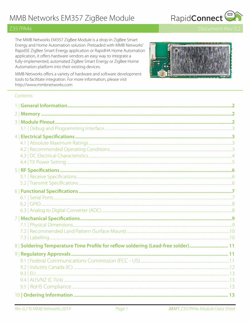
Page 1 Rev 0.2 © MMB Networks 2014 DRAFT Z357PA4x Module Data Sheet MMB Networks EM357 ZigBee Module Z357PA4x Document Rev 0.2 The MMB Networks EM357 ZigBee Module is a drop-in ZigBee Smart Energy and Home Automation solution. Preloaded with MMB Networks’ RapidSE ZigBee Smart Energy application or RapidHA Home Automation application, it offers hardware vendors an easy way to integrate a fully-implemented, automated ZigBee Smart Energy or ZigBee Home Automation platform into their existing devices. MMB Networks offers a variety of hardware and software development tools to facilitate integration. For more information, please visit http://www.mmbnetworks.com Contents 1 | General Information...................................................................................................................................2 2 | Memory ........................................................................................................................................................2 3 | Module Pinout .............................................................................................................................................2 3.1 | Debug and Programming Interface ..........................................................................................................................................3 4 | Electrical Specifications .............................................................................................................................3 4.1 | Absolute Maximum Ratings ...........................................................................................................................................................3 4.2 | Recommended Operating Conditions ....................................................................................................................................3 4.3 | DC Electrical Characteristics ...........................................................................................................................................................4 4.4 | TX Power Setting ...................................................................................................................................................................................5 5 | RF Specifications .........................................................................................................................................6 5.1 | Receive Specifications ........................................................................................................................................................................6 5.2 | Transmit Specifications ......................................................................................................................................................................6 6 | Functional Specifications ..........................................................................................................................7 6.1 | Serial Ports .................................................................................................................................................................................................7 6.2 | GPIO...............................................................................................................................................................................................................8 6.3 | Analog to Digital Converter (ADC) .............................................................................................................................................8 7 | Mechanical Specifications.........................................................................................................................9 7.1 | Physical Dimensions ............................................................................................................................................................................9 7.2 | Recommended Land Pattern (Surface Mount) ............................................................................................................... 10 7.3 | Labelling .................................................................................................................................................................................................. 10 8 | Soldering Temperature Time Profile for reflow soldering (Lead-free solder)............................... 11 9 | Regulatory Approvals ............................................................................................................................. 11 9.1 | Federal Communications Commission (FCC - US) ......................................................................................... 11 9.2 | Industry Canada (IC) ........................................................................................................................................................................ 12 9.3 | EU ................................................................................................................................................................................................................. 13 9.4 | AUS/NZ (C-Tick) ................................................................................................................................................................................... 13 9.5 | RoHS Compliance .............................................................................................................................................................. 13 10 | Ordering Information ........................................................................................................................... 13
Transcript of MMB Networks EM357 ZigBee Module - Squarespace 0.2 MMB Networks 2014 Page 1 DRAFT 357PA4 Module ata...
Page 1Rev 0.2 © MMB Networks 2014 DRAFT Z357PA4x Module Data Sheet
MMB Networks EM357 ZigBee ModuleZ357PA4x Document Rev 0.2
The MMB Networks EM357 ZigBee Module is a drop-in ZigBee Smart Energy and Home Automation solution. Preloaded with MMB Networks’ RapidSE ZigBee Smart Energy application or RapidHA Home Automation application, it offers hardware vendors an easy way to integrate a fully-implemented, automated ZigBee Smart Energy or ZigBee Home Automation platform into their existing devices.
MMB Networks offers a variety of hardware and software development tools to facilitate integration. For more information, please visit http://www.mmbnetworks.com
Contents
1 | General Information ...................................................................................................................................2
2 | Memory ........................................................................................................................................................2
3 | Module Pinout .............................................................................................................................................23.1 | Debug and Programming Interface ..........................................................................................................................................3
4 | Electrical Specifications .............................................................................................................................34.1 | Absolute Maximum Ratings ...........................................................................................................................................................34.2 | Recommended Operating Conditions ....................................................................................................................................34.3 | DC Electrical Characteristics ...........................................................................................................................................................44.4 | TX Power Setting ...................................................................................................................................................................................5
5 | RF Specifications .........................................................................................................................................65.1 | Receive Specifications ........................................................................................................................................................................65.2 | Transmit Specifications ......................................................................................................................................................................6
6 | Functional Specifications ..........................................................................................................................76.1 | Serial Ports .................................................................................................................................................................................................76.2 | GPIO ...............................................................................................................................................................................................................86.3 | Analog to Digital Converter (ADC) .............................................................................................................................................8
7 | Mechanical Specifications .........................................................................................................................97.1 | Physical Dimensions ............................................................................................................................................................................97.2 | Recommended Land Pattern (Surface Mount) ...............................................................................................................107.3 | Labelling ..................................................................................................................................................................................................10
8 | Soldering Temperature Time Profile for reflow soldering (Lead-free solder)............................... 11
9 | Regulatory Approvals ............................................................................................................................. 119.1 | Federal Communications Commission (FCC - US) .........................................................................................119.2 | Industry Canada (IC) ........................................................................................................................................................................129.3 | EU .................................................................................................................................................................................................................139.4 | AUS/NZ (C-Tick) ...................................................................................................................................................................................139.5 | RoHS Compliance ..............................................................................................................................................................13
10 | Ordering Information ........................................................................................................................... 13
Page 2Rev 0.2 © MMB Networks 2014 DRAFT Z357PA4x Module Data Sheet
1 | General Information
Note that some of the specifications refer to either EM357 or Module. Please note specifications cited as EM357 are taken from the EM357 datasheet (this should also be noted where referred to). Module means measurements taken with our production module.
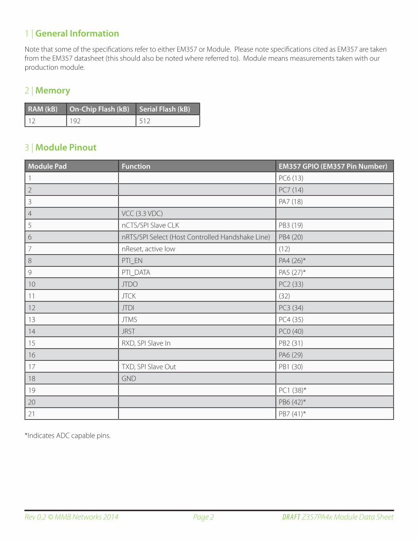
2 | Memory
3 | Module Pinout
RAM (kB) On-Chip Flash (kB) Serial Flash (kB)
12 192 512
Module Pad Function EM357 GPIO (EM357 Pin Number)
1 PC6 (13)
2 PC7 (14)
3 PA7 (18)
4 VCC (3.3 VDC)
5 nCTS/SPI Slave CLK PB3 (19)
6 nRTS/SPI Select (Host Controlled Handshake Line) PB4 (20)
7 nReset, active low (12)
8 PTI_EN PA4 (26)*
9 PTI_DATA PA5 (27)*
10 JTDO PC2 (33)
11 JTCK (32)
12 JTDI PC3 (34)
13 JTMS PC4 (35)
14 JRST PC0 (40)
15 RXD, SPI Slave In PB2 (31)
16 PA6 (29)
17 TXD, SPI Slave Out PB1 (30)
18 GND
19 PC1 (38)*
20 PB6 (42)*
21 PB7 (41)*
*Indicates ADC capable pins.
Page 3Rev 0.2 © MMB Networks 2014 DRAFT Z357PA4x Module Data Sheet
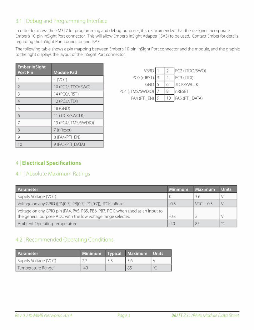
3.1 | Debug and Programming Interface
In order to access the EM357 for programming and debug purposes, it is recommended that the designer incorporate Ember’s 10-pin InSight Port connector. This will allow Ember’s InSight Adapter (ISA3) to be used. Contact Ember for details regarding the InSight Port connector and ISA3.
The following table shows a pin mapping between Ember’s 10-pin InSight Port connector and the module, and the graphic to the right displays the layout of the InSight Port connector.
4 | Electrical Specifications
4.1 | Absolute Maximum Ratings
4.2 | Recommended Operating Conditions
Ember InSight Port Pin Module Pad
1 4 (VCC)
2 10 (PC2/JTDO/SWO)
3 14 (PC0/JRST)
4 12 (PC3/JTDI)
5 18 (GND)
6 11 (JTCK/SWCLK)
7 13 (PC4/JTMS/SWDIO)
8 7 (nReset)
9 8 (PA4/PTI_EN)
10 9 (PA5/PTI_DATA)
Parameter Minimum Maximum Units
Supply Voltage (VCC) 0 3.6 V
Voltage on any GPIO ([PA[0:7], PB[0:7], PC[0:7]), JTCK, nReset -0.3 VCC + 0.3 V
Voltage on any GPIO pin (PA4, PA5, PB5, PB6, PB7, PC1) when used as an input to the general purpose ADC with the low voltage range selected -0.3 2 V
Ambient Operating Temperature -40 85 °C
Parameter Minimum Typical Maximum Units
Supply Voltage (VCC) 2.7 3.3 3.6 V
Temperature Range -40 85 °C
1 2
3 4
5 6
7 8
9 10
VBRD
PC0 (nJRST)
GND
PC4 (JTMS/SWDIO)
PA4 (PTI_EN)
PC2 (JTDO/SWO)
PC3 (JTDI)
JTCK/SWCLK
nRESET
PA5 (PTI_DATA)
Page 4Rev 0.2 © MMB Networks 2014 DRAFT Z357PA4x Module Data Sheet
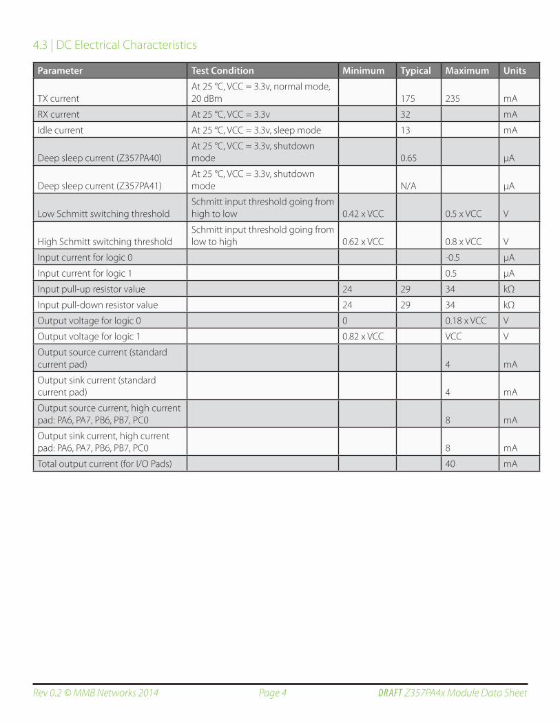
Parameter Test Condition Minimum Typical Maximum Units
TX currentAt 25 °C, VCC = 3.3v, normal mode, 20 dBm 175 235 mA
RX current At 25 °C, VCC = 3.3v 32 mA
Idle current At 25 °C, VCC = 3.3v, sleep mode 13 mA
Deep sleep current (Z357PA40)At 25 °C, VCC = 3.3v, shutdown mode 0.65 μA
Deep sleep current (Z357PA41)At 25 °C, VCC = 3.3v, shutdown mode N/A μA
Low Schmitt switching thresholdSchmitt input threshold going from high to low 0.42 x VCC 0.5 x VCC V
High Schmitt switching thresholdSchmitt input threshold going from low to high 0.62 x VCC 0.8 x VCC V
Input current for logic 0 -0.5 μA
Input current for logic 1 0.5 μA
Input pull-up resistor value 24 29 34 kΩ
Input pull-down resistor value 24 29 34 kΩ
Output voltage for logic 0 0 0.18 x VCC V
Output voltage for logic 1 0.82 x VCC VCC V
Output source current (standard current pad) 4 mA
Output sink current (standard current pad) 4 mA
Output source current, high current pad: PA6, PA7, PB6, PB7, PC0 8 mA
Output sink current, high current pad: PA6, PA7, PB6, PB7, PC0 8 mA
Total output current (for I/O Pads) 40 mA
4.3 | DC Electrical Characteristics
Page 5Rev 0.2 © MMB Networks 2014 DRAFT Z357PA4x Module Data Sheet
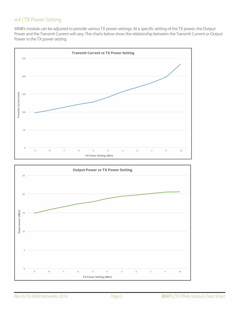
4.4 | TX Power Setting
MMB’s module can be adjusted to provide various TX power settings. At a specific setting of the TX power, the Output Power and the Transmit Current will vary. The charts below show the relationship between the Transmit Current or Output Power vs the TX power setting.
0
50
100
150
200
250
-‐9 -‐8 -‐7 -‐6 -‐5 -‐4 -‐3 -‐2 -‐1 0 +3
Tran
smit
Cur
rent
(mA
)
TX Power Setting (dBm)
Transmit Current vs TX Power Setting
0
5
10
15
20
25
-‐9 -‐8 -‐7 -‐6 -‐5 -‐4 -‐3 -‐2 -‐1 0 +3
Oup
ut p
ower
(dBm
)
TX Power Setting (dBm)
Output Power vs TX Power Setting
Page 6Rev 0.2 © MMB Networks 2014 DRAFT Z357PA4x Module Data Sheet
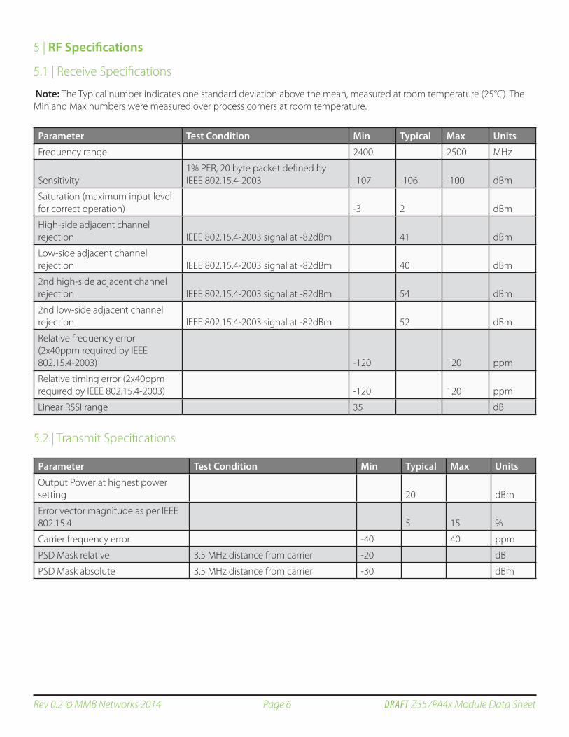
5 | RF Specifications
5.1 | Receive Specifications
Note: The Typical number indicates one standard deviation above the mean, measured at room temperature (25°C). The Min and Max numbers were measured over process corners at room temperature.
5.2 | Transmit Specifications
Parameter Test Condition Min Typical Max Units
Frequency range 2400 2500 MHz
Sensitivity1% PER, 20 byte packet defined by IEEE 802.15.4-2003 -107 -106 -100 dBm
Saturation (maximum input level for correct operation) -3 2 dBm
High-side adjacent channel rejection IEEE 802.15.4-2003 signal at -82dBm 41 dBm
Low-side adjacent channel rejection IEEE 802.15.4-2003 signal at -82dBm 40 dBm
2nd high-side adjacent channel rejection IEEE 802.15.4-2003 signal at -82dBm 54 dBm
2nd low-side adjacent channel rejection IEEE 802.15.4-2003 signal at -82dBm 52 dBm
Relative frequency error (2x40ppm required by IEEE 802.15.4-2003) -120 120 ppm
Relative timing error (2x40ppm required by IEEE 802.15.4-2003) -120 120 ppm
Linear RSSI range 35 dB
Parameter Test Condition Min Typical Max Units
Output Power at highest power setting 20 dBm
Error vector magnitude as per IEEE 802.15.4 5 15 %
Carrier frequency error -40 40 ppm
PSD Mask relative 3.5 MHz distance from carrier -20 dB
PSD Mask absolute 3.5 MHz distance from carrier -30 dBm
Page 7Rev 0.2 © MMB Networks 2014 DRAFT Z357PA4x Module Data Sheet
6 | Functional Specifications
6.1 | Serial PortsRefer to the EM357 data sheet for functionality and associated GPIO pin outs.
Note: The module pin out table in section 3 of this document provides a cross reference between the MMB module pins and the EM357 GPIO.
6.1.1 | SC1 Serial Controller (UART, SPI)
The SC1 module provides UART or SPI (master or slave) serial communications.
Serial Controller Features
The SC1 UART supports the following features:• Baud rate (300 bps up to 921.6 kbps) (*Note: these values are provided to show the hardware capability. RapidSE and
RapidHA do not provide the ability to modify the baud rate from the default value of 115.2 kbps. However, MMB can adjust it as necessary through a Non-Recurring Engineering engagement)
• Data bits (7 or 8)• Parity bits (none, odd, or even)• Stop bits (1 or 2)• False start bit and noise filtering• Receive and transmit FIFOs• Optional CTS/RTS flow control• Receiver and transmit DMA channels• GPIO signals:
ʳ TXD (serial data out) ʳ RXD (serial data in) ʳ nRTS (optional) ʳ nCTS (optional)
The SPI slave controller has the following features:• Full duplex operation• Up to 4 Mbps data transfer rate• Programmable clock polarity and clock phase• Selectable data shift direction (either LSB or MSB first)• Slave select input• The following signals can be made available on the GPIO pins:
ʳ MOSI (serial data in) ʳ MISO (serial data out) ʳ SCLK (serial clock in) ʳ nSSEL (slave select)
The SPI master controller has the following features: (*Note: the SPI master controller data is provided to show the hardware capability. RapidSE and RapidHA are configured as a SPI Slave, not Master) • Full duplex operation• Programmable clock frequency (12 MHz max.)• Programmable clock polarity and clock phase• Selectable data shift direction (either LSB or MSB first)• Receive and transmit FIFOs• Receive and transmit DMA channels• The following signals can be made available on the GPIO pins:
ʳ MOSI (serial data out) ʳ MISO (serial data in) ʳ MCLK (serial clock out)
Page 8Rev 0.2 © MMB Networks 2014 DRAFT Z357PA4x Module Data Sheet
Both EM35x serial controllers SC1 and SC2 include a Two Wire serial Interface (TWI) master controller with the following features: (*Note: Current MMB modules are not configured to support TWI/I2C. Please contact MMB for further information.)• Uses only two bidirectional GPIO pins• Programmable clock frequency (up to 400 kHz)• Supports both 7-bit and 10-bit addressing• Compatible with Philips’ I2C-bus slave devices
6.2 | GPIO
The EM357 has multi-purpose GPIO pins that may be individually configured as:• General purpose output • General purpose open-drain output • Alternate output controlled by a peripheral device • Alternate open-drain output controlled by a peripheral device • Analog • General purpose input • General purpose input with pull-up or pull-down resistor
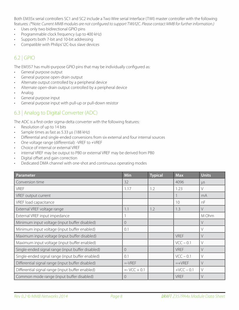
6.3 | Analog to Digital Converter (ADC)
The ADC is a first-order sigma-delta converter with the following features:• Resolution of up to 14 bits • Sample times as fast as 5.33 μs (188 kHz) • Differential and single-ended conversions from six external and four internal sources • One voltage range (differential): -VREF to +VREF • Choice of internal or external VREF • internal VREF may be output to PB0 or external VREF may be derived from PB0 • Digital offset and gain correction • Dedicated DMA channel with one-shot and continuous operating modes
Parameter Min Typical Max Units
Conversion time 32 4096 μs
VREF 1.17 1.2 1.23 V
VREF output current 1 mA
VREF load capacitance 10 nF
External VREF voltage range 1.1 1.2 1.3 V
External VREF input impedance 1 M Ohm
Minimum input voltage (input buffer disabled) 0 V
Minimum input voltage (input buffer enabled) 0.1 V
Maximum input voltage (input buffer disabled) VREF V
Maximum input voltage (input buffer enabled) VCC – 0.1 V
Single-ended signal range (input buffer disabled) 0 VREF V
Single-ended signal range (input buffer enabled) 0.1 VCC – 0.1 V
Differential signal range (input buffer disabled) =-VREF =+VREF V
Differential signal range (input buffer enabled) =- VCC + 0.1 +VCC – 0.1 V
Common mode range (input buffer disabled) 0 VREF V
Page 9Rev 0.2 © MMB Networks 2014 DRAFT Z357PA4x Module Data Sheet
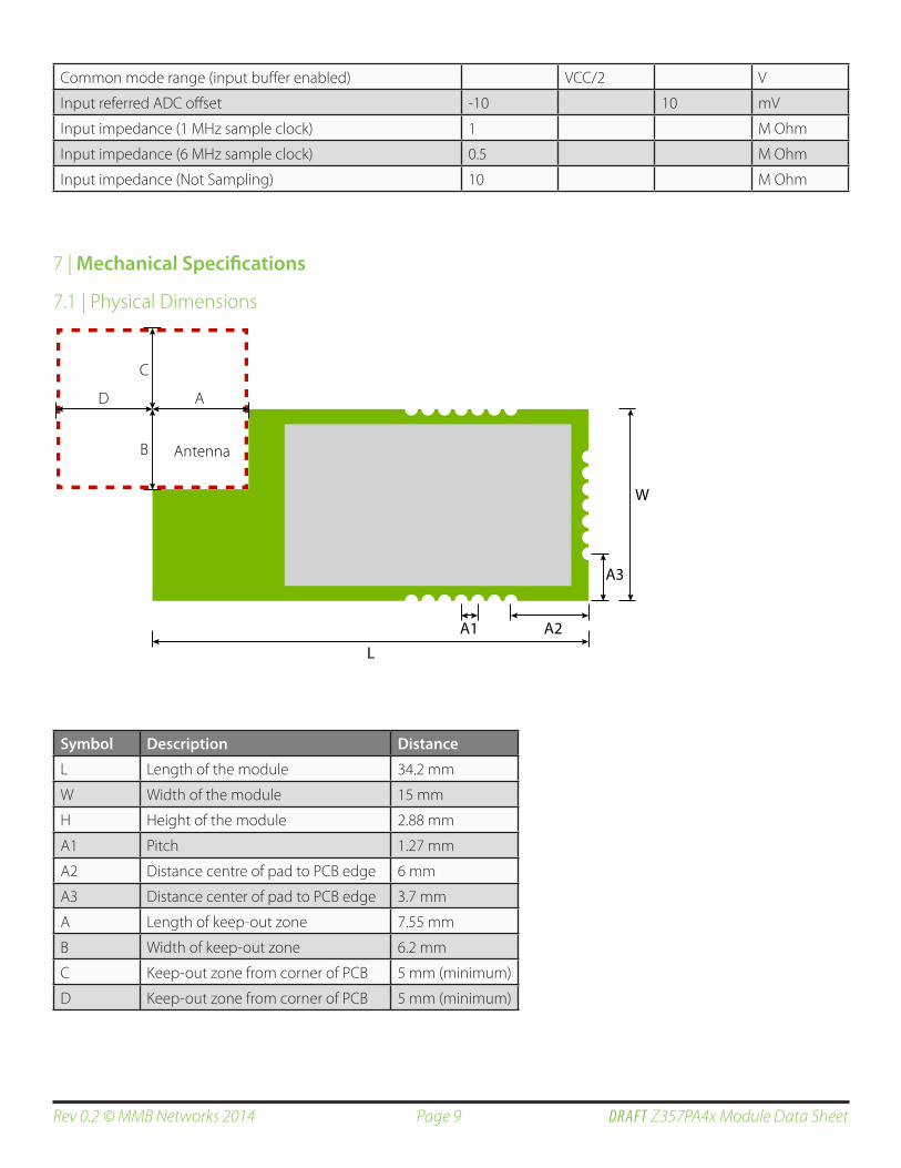
7 | Mechanical Specifications
7.1 | Physical Dimensions
Antenna
A
B
D
C
L
W
A3
A1 A2
Symbol Description Distance
L Length of the module 34.2 mm
W Width of the module 15 mm
H Height of the module 2.88 mm
A1 Pitch 1.27 mm
A2 Distance centre of pad to PCB edge 6 mm
A3 Distance center of pad to PCB edge 3.7 mm
A Length of keep-out zone 7.55 mm
B Width of keep-out zone 6.2 mm
C Keep-out zone from corner of PCB 5 mm (minimum)
D Keep-out zone from corner of PCB 5 mm (minimum)
Common mode range (input buffer enabled) VCC/2 V
Input referred ADC offset -10 10 mV
Input impedance (1 MHz sample clock) 1 M Ohm
Input impedance (6 MHz sample clock) 0.5 M Ohm
Input impedance (Not Sampling) 10 M Ohm
Page 10Rev 0.2 © MMB Networks 2014 DRAFT Z357PA4x Module Data Sheet
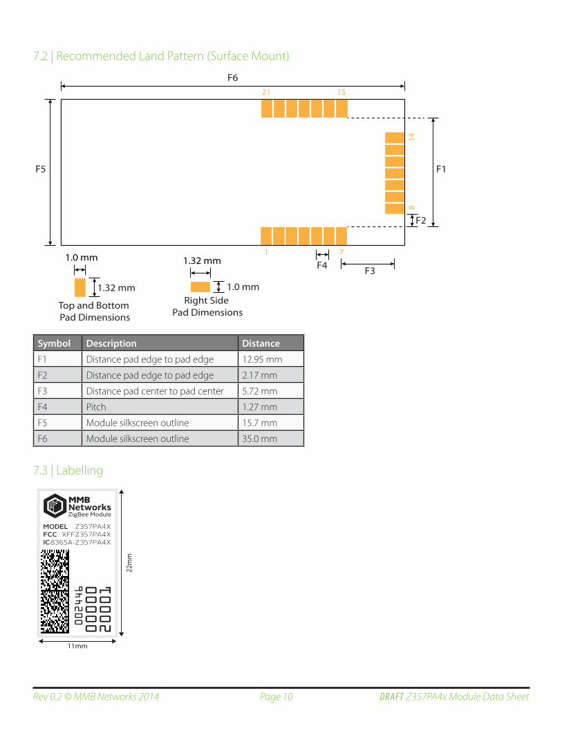
7.2 | Recommended Land Pattern (Surface Mount)
F5 F1
F2
F3F4
F6
Top and Bottom Pad Dimensions
1.0 mm
1.32 mm
1 7
21 15
148
Right Side Pad Dimensions
1.32 mm
1.0 mm
Symbol Description Distance
F1 Distance pad edge to pad edge 12.95 mm
F2 Distance pad edge to pad edge 2.17 mm
F3 Distance pad center to pad center 5.72 mm
F4 Pitch 1.27 mm
F5 Module silkscreen outline 15.7 mm
F6 Module silkscreen outline 35.0 mm
7.3 | Labelling
Z357PA4XMODELFCCIC
XFFZ357PA4X8365A-Z357PA4X
11mm
22m
m
Page 11Rev 0.2 © MMB Networks 2014 DRAFT Z357PA4x Module Data Sheet
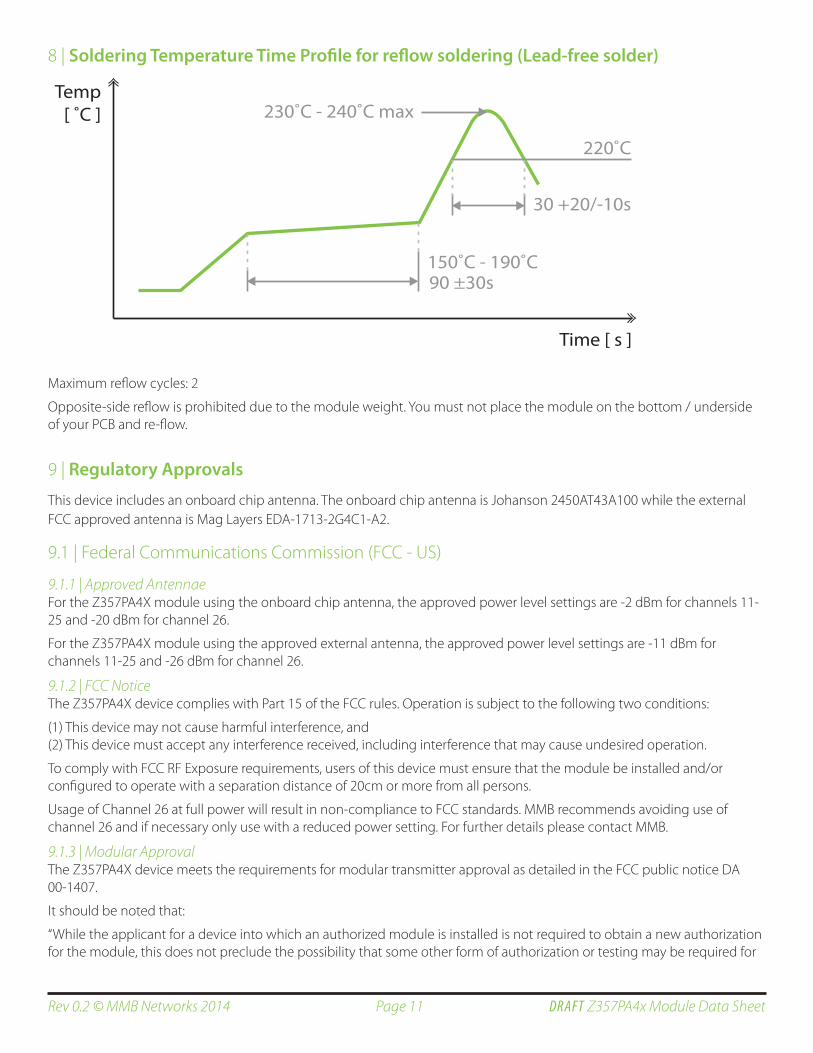
8 | Soldering Temperature Time Profile for reflow soldering (Lead-free solder)
150˚C - 190˚C
220˚C
30 +20/-10s
90 ±30s
230˚C - 240˚C maxTemp
[ ˚C ]
Time [ s ]
Maximum reflow cycles: 2
Opposite-side reflow is prohibited due to the module weight. You must not place the module on the bottom / underside of your PCB and re-flow.
9 | Regulatory Approvals
This device includes an onboard chip antenna. The onboard chip antenna is Johanson 2450AT43A100 while the external FCC approved antenna is Mag Layers EDA-1713-2G4C1-A2.
9.1 | Federal Communications Commission (FCC - US)
9.1.1 | Approved AntennaeFor the Z357PA4X module using the onboard chip antenna, the approved power level settings are -2 dBm for channels 11-25 and -20 dBm for channel 26.
For the Z357PA4X module using the approved external antenna, the approved power level settings are -11 dBm for channels 11-25 and -26 dBm for channel 26.
9.1.2 | FCC NoticeThe Z357PA4X device complies with Part 15 of the FCC rules. Operation is subject to the following two conditions:
(1) This device may not cause harmful interference, and (2) This device must accept any interference received, including interference that may cause undesired operation.
To comply with FCC RF Exposure requirements, users of this device must ensure that the module be installed and/or configured to operate with a separation distance of 20cm or more from all persons.
Usage of Channel 26 at full power will result in non-compliance to FCC standards. MMB recommends avoiding use of channel 26 and if necessary only use with a reduced power setting. For further details please contact MMB.
9.1.3 | Modular Approval The Z357PA4X device meets the requirements for modular transmitter approval as detailed in the FCC public notice DA 00-1407.
It should be noted that:
“While the applicant for a device into which an authorized module is installed is not required to obtain a new authorization for the module, this does not preclude the possibility that some other form of authorization or testing may be required for

Page 12Rev 0.2 © MMB Networks 2014 DRAFT Z357PA4x Module Data Sheet
the device (e.g., a WLAN into which an authorized module is installed must still be authorized as a PC peripheral, subject to the appropriate equipment authorization).” -- FCC Public Notice DA 00-1407
Caution: Changes or modifications not expressly approved by the party responsible for compliance could void the user’s authority to operate the equipment.
9.1.4 | Labeling Requirements The user of this device is responsible for meeting the FCC labeling requirements. A clearly visible label on the exterior enclosure of an incorporating device must list the MMB Research Inc. FCC ID “XFFZ357PA4X” and the FCC Notice above (section 9.1.1).
The exterior label should use the wording “Contains” or “Contains Transmitter Module”. For example:
Contains FCC ID: XFFZ357PA4XorContains Transmitter Module FCC ID: XFFZ357PA4X
Any similar wording that expresses the same meaning may be used.
9.2 | Industry Canada (IC)
9.2.1 | Approved AntennaeFor the Z357PA4X module using the onboard chip antenna, the approved power level settings are -2 dBm for channels 11-25 and -20 dBm for channel 26.
For the Z357PA4X module using the approved external antenna, the approved power level settings are -11 dBm for channels 11-25 and -26 dBm for channel 26.
9.2.2 | IC NoticeThis device complies with Industry Canada licence-exempt RSS standard(s).
Operation is subject to the following two conditions:
(1) this device may not cause interference, and(2) this device must accept any interference, including interference that may cause undesired operation of the device.
Le présent appareil est conforme aux CNR d’Industrie Canada applicables aux appareils radio exempts de licence.
L’exploitation est autorisée aux deux conditions suivantes :
(1) l’appareil ne doit pas produire de brouillage, et (2) l’utilisateur de l’appareil doit accepter tout brouillage radioélectrique subi, même si le brouillage est susceptible d’en compromettre le fonctionnement.
9.2.3 | Labeling Requirements
The host device shall be properly labelled to identify the modules within the host device. The Industry Canada certification label of a module shall be clearly visible at all times when installed in the host device, otherwise the host device must be labelled to display the Industry Canada certification number of the module, preceded by the words “Contains transmitter module”, or the word “Contains”, or similar wording expressing the same meaning, as follows:
Contains transmitter module IC: 8365A-Z357PA4x
Page 13Rev 0.2 © MMB Networks 2014 DRAFT Z357PA4x Module Data Sheet
Copyright © 2014 MMB Research Inc. All rights reserved.
The information in this document is subject to change without notice. This document is believed to be accurate and reliable, but the statements contained herein are
presented without expressed or implied warranty.MMB Networks is a division of MMB Research Inc.
MMB Networks is a division of MMB Research Inc RapidSE, RapidHA, and RapidConnect are trademarks of MMB Research Inc.
All other trademarks are the property of their respective holders.November 2014
500 -243 Colleget Street
Toronto, Ontario, Canada
M5T 1R5
416.636.3145
www.mmbnetworks.com
9.3 | EU
This device is compliant with the following EU standards: ETSI EN 300 328 (v1.9.1), ETSI EN 301 489 1 (v1.9.2) and ETSI EN 301 489 17 (v2.2.1), provided that the transmit power level is set to -2 dBm (if on-board antenna is used) or -11 dBm (if whip antenna is used).
9.4 | AUS/NZ (C-Tick)
The Z357PA4X module have been certified to be used in Australia and New Zealand.
9.5 | RoHS Compliance
The Z357PA4X device does not contain any substances in excess of the maximum concentration allowed by Directive 2002/95/EC. The module is RoHS compliant.
10 | Ordering Information
SKU Deep Sleep Optimization Antenna Option
Z357PA41-SMT No Chip
Z357PA41-UFL No U.FL
Z357PA40-SMT Yes Chip
Z357PA40-UFL Yes U.FL