
Minimize power losses of lightly loaded flyback converters ...€¦ · optimized for flyback...
24
INTRODUCTION The minimization of the power drawn from the mains under light load conditions (Standby, Suspend or some other idle mode) is an issue that is recently becoming of great interest, above all else because new and more severe standards are coming into force. This is already well-established in the area of computer monitors, where norms define precisely the vari- ous idle modes and the relevant maximum consumption admitted, but more and more often power sup- plies for other pieces of office equipment (i.e. printers, photocopiers, fax machines, AC-DC adaptors, etc.), are required to accomplish with specifications concerning energy saving. Anyway, minimizing the power wasted by a lightly loaded switch-mode converter is a demanding chal- lenge for power supply designers and, to achieve the goal, an appropriate design strategy is required. March 2000 ® AN1049 APPLICATION NOTE MINIMIZE POWER LOSSES OF LIGHTLY LOADED FLYBACK CONVERTERS WITH THE L5991 PWM CONTROLLER by Claudio Adragna The L5991 PWM controller is particularly suitable for SMPS of equipment that must comply with standards concerning energy saving. The device, optimized for flyback topology, monitors the power demanded by the load and changes the operating frequency of the converter accordingly: high fre- quency at heavy load, low frequency at light load. In this way, power losses dependent on frequency are reduced at light load maintaining, at the same time, the advantages offered by a high switching frequency at heavy load. The frequency reduction is very helpful but is not the only means needed to minimize power losses. This note surveys the above mentioned functionality of the L5991 (called "Standby" function) as well as the most significant points to consider in order to achieve the goal of a very efficient lightly loaded flyback. + - TIMING 2 3 + - 14 T Vref CLK 2.5V + - 1.2V 13 BLANKING PWM FAULT SOFT-START R S Q 21V 10V VREF OK DIS + - E/A 1V R 2R DIS 2.5V 7 6 5 11 10 9 4 8 15 1 17V + - PWM UVLO 12 SGND COMP SS ISEN DIS DC RCT SYNC DC-LIM VCC VREF VFB PGND OUT VC OVER CURRENT 16 ST-BY VREF STANDBY + - STANDBY 2.5/4.0V Figure 1. L5991 Internal Block Diagram 1/24
Transcript of Minimize power losses of lightly loaded flyback converters ...€¦ · optimized for flyback...

INTRODUCTION
The minimization of the power drawn from the mains under light load conditions (Standby, Suspend orsome other idle mode) is an issue that is recently becoming of great interest, above all else becausenew and more severe standards are coming into force.This is already well-established in the area of computer monitors, where norms define precisely the vari-ous idle modes and the relevant maximum consumption admitted, but more and more often power sup-plies for other pieces of office equipment (i.e. printers, photocopiers, fax machines, AC-DC adaptors,etc.), are required to accomplish with specifications concerning energy saving.
Anyway, minimizing the power wasted by a lightly loaded switch-mode converter is a demanding chal-lenge for power supply designers and, to achieve the goal, an appropriate design strategy is required.
March 2000
®
AN1049APPLICATION NOTE
MINIMIZE POWER LOSSES OF LIGHTLY LOADED FLYBACKCONVERTERS WITH THE L5991 PWM CONTROLLER
by Claudio Adragna
The L5991 PWM controller is particularly suitable for SMPS of equipment that must comply withstandards concerning energy saving. The device, optimized for flyback topology, monitors the powerdemanded by the load and changes the operating frequency of the converter accordingly: high fre-quency at heavy load, low frequency at light load. In this way, power losses dependent on frequency are reduced at light load maintaining, at the sametime, the advantages offered by a high switching frequency at heavy load.The frequency reduction is very helpful but is not the only means needed to minimize power losses.This note surveys the above mentioned functionality of the L5991 (called "Standby" function) as wellas the most significant points to consider in order to achieve the goal of a very efficient lightly loadedflyback.
+
-
TIMING2
3
+
-14
T
Vref
CLK
2.5V
+
-1.2V
13
BLANKING
PWM
FAULT SOFT-START
R
S Q
21V
10V
VREF OK
DIS
+
-E/A
1V R2R
DIS
2.5V7
6
5
11
10
9
48151
17V
+
-
PWM
UVLO
12
SGND COMP
SS
ISEN
DIS
DC
RCT
SYNC DC-LIM VCC VREF
VFB
PGND
OUT
VC
OVER CURRENT
16ST-BY
VREF
STANDBY
+
-
STANDBY
2.5/4.0V
Figure 1. L5991 Internal Block Diagram
1/24

The key point of this strategy is a low switching frequency. It is well-known that many of the power losssources in a lightly loaded flyback waste energy proportionally to the switching frequency, hence thisshould be reduced as much as possible. On the other hand, it is equally well-known that a low switchingfrequency leads to bigger and heavier magnetics and makes filtering more troublesome.It is then desirable to make the system operate at high frequency under nominal load condition and toreduce the frequency when the system works in a low-consumption mode. This requires a special func-tionality of the controller: it should be able to recognize automatically the condition of light or heavy loadand should adequate its operating frequency accordingly. The L5991 PWM controller, with its "Standby function", meets exactly this requirement. The function isoptimized for flyback topology: in fact, power supply of office equipment lies most often in the medium-low power range, where flyback topology features the lowest cost/performance ratio and is, therefore,the favorite one. However, the goal of power losses minimization cannot be achieved with only a simple reduction of theswitching frequency. Although the most important, this is only one of the numerous points of a wide-ranging strategy that must be looked into on the whole.This application note is composed of two distinct parts. The first part deals with the L5991, describes theoperation of the "Standby function" in detail and states several relationships useful for the design. Thesecond one provides an overview of the points to be considered in the above mentioned strategy, aswell as a number of tips that can be helpful.
1) DESIGNING WITH THE L5991 PWM CONTROLLERThe L5991The device, whose internal block diagram is shown in fig. 1, is based on a standard "peak" currentmode PWM controller, such as the UC384x family, with the addition of numerous ancillary featuresamong which Standby function is the most noticeable.The L5991, which is available in DIP16 and SO16N packages, features the following characteristics:
Very low start-up current (75 µA typ. - 120 µA max.) ;low quiescent current (7 mA typ. - 10 mA max.) ;internal reference with 1% precision guaranteed (@ Tj=25°C);high current capability, large bandwidth, high slew-rate error amplifier;high-speed current loop (< 100 ns delay to output);high current capability totem-pole output for MOSFET or IGBT drive;Standby function ;IN/OUT synchronization;precise maximum duty cycle control;programmable soft-start100 ns Leading Edge Blanking on current sense for increased noise immunity;overcurrent protection with soft-start intervention;latched disable function;
All these characteristics are described in detail in the datasheet of the device. In this context, however, itis worth emphasizing the low current consumption of the device, both before start-up and when running.Along with the standby function, the low consumption turns out to be particularly useful for minimizinglosses.Table 1 compares these characteristics with the UC384XA/B family.Table 1. L5991 vs. UC384XA/B family
CONTROLLER START-UP CURRENT QUIESCENT CURRENT STANDBY FUNCTION
L5991 75µA typ.120µA max.
7.0mA typ.10.0mA max.
yes
UC384XA/B 300µA typ.500µA max.
12mA typ.17mA max.
no
AN1049 APPLICATION NOTE
2/24
The L5991 can be used in off-line SMPS’ with any single-ended topology. However, its features makethe device particularly useful for power supplies based on flyback topology for office equipment thatmust comply with standards concerning energy saving. Monitor displays, printers, photocopiers, scan-ners and fax machines are the most noticeable examples.
Standby function description
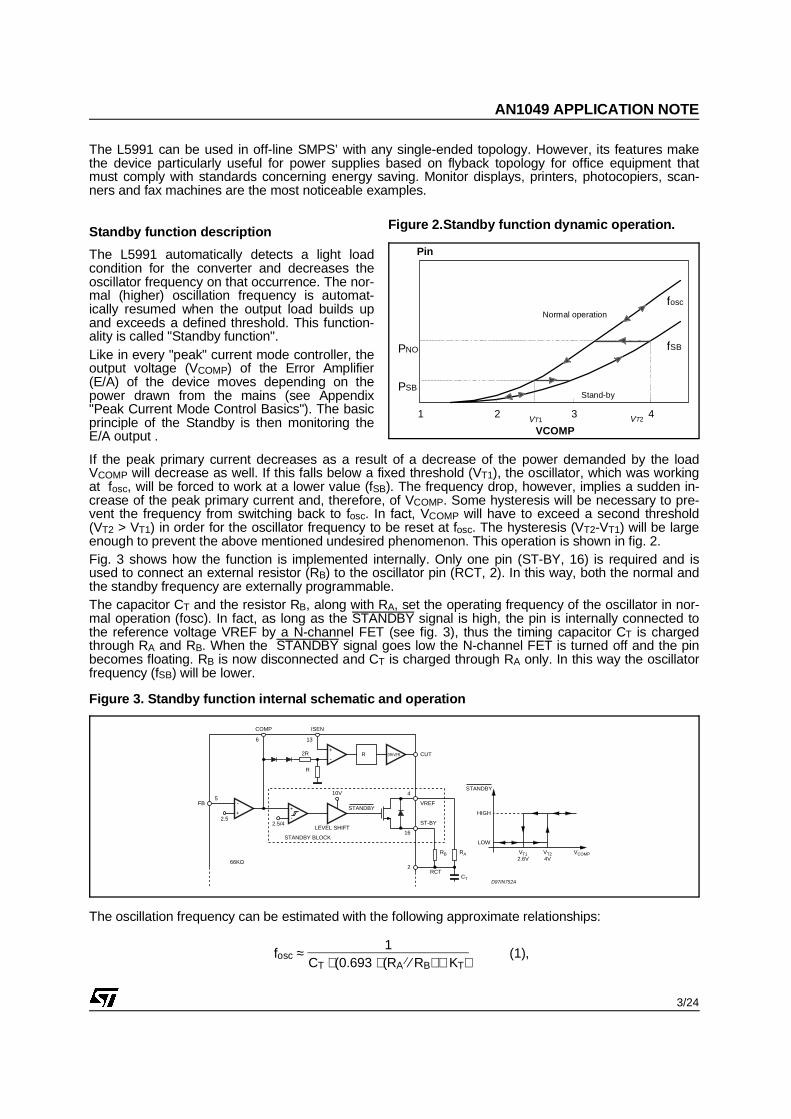
The L5991 automatically detects a light loadcondition for the converter and decreases theoscillator frequency on that occurrence. The nor-mal (higher) oscillation frequency is automat-ically resumed when the output load builds upand exceeds a defined threshold. This function-ality is called "Standby function". Like in every "peak" current mode controller, theoutput voltage (VCOMP) of the Error Amplifier(E/A) of the device moves depending on thepower drawn from the mains (see Appendix"Peak Current Mode Control Basics"). The basicprinciple of the Standby is then monitoring theE/A output .
If the peak primary current decreases as a result of a decrease of the power demanded by the loadVCOMP will decrease as well. If this falls below a fixed threshold (VT1), the oscillator, which was workingat fosc, will be forced to work at a lower value (fSB). The frequency drop, however, implies a sudden in-crease of the peak primary current and, therefore, of VCOMP. Some hysteresis will be necessary to pre-vent the frequency from switching back to fosc. In fact, VCOMP will have to exceed a second threshold(VT2 > VT1) in order for the oscillator frequency to be reset at fosc. The hysteresis (VT2-VT1) will be largeenough to prevent the above mentioned undesired phenomenon. This operation is shown in fig. 2.Fig. 3 shows how the function is implemented internally. Only one pin (ST-BY, 16) is required and isused to connect an external resistor (RB) to the oscillator pin (RCT, 2). In this way, both the normal andthe standby frequency are externally programmable. The capacitor CT and the resistor RB, along with RA, set the operating frequency of the oscillator in nor-mal operation (fosc). In fact, as long as the STANDBY signal is high, the pin is internally connected tothe reference voltage VREF by a N-channel FET (see fig. 3), thus the timing capacitor CT is chargedthrough RA and RB. When the STANDBY signal goes low the N-channel FET is turned off and the pinbecomes floating. RB is now disconnected and CT is charged through RA only. In this way the oscillatorfrequency (fSB) will be lower.
The oscillation frequency can be estimated with the following approximate relationships:
fosc ≈ 1
CT ⋅ (0.693 ⋅ (RA ⁄ ⁄ RB) + KT)
(1),
1 2 3 4
VCOMP
Pin
fosc
fSB
Stand-by
Normal operation
VT1
PNO
PSB
VT2
Figure 2.Standby function dynamic operation.
-
+ -
+
2.52.5/4
66KΩ
R
STANDBY
10V
LEVEL SHIFT
COMP
FB VREF
ST-BY
4
16
6
RCTCT
RARB
2
5
LOW
HIGH
STANDBY
D97IN752A
VT12.6V
VT24V
VCOMP
-
+
ISEN
13
R DRIVER CUT
STANDBY BLOCK
2R
Figure 3. Standby function internal schematic and operation
AN1049 APPLICATION NOTE
3/24

which gives the normal operating frequency, and:
fSB ≈ 1
CT ⋅ (0.693 ⋅ RA + KT) (2)
which gives the standby operating frequency, that is the one the converter will operate at when lightlyloaded. In the above expressions, RA // RB means:
RA ⁄ ⁄ RB =
RA ⋅ RB
RA + RB (3),
and KT, defined as:
KT =
90, V15 = VREF160, V15 = GND/OPEN
(4)
is related to the duration of the falling-edge of the sawtooth. In case V15 is connected to VREF, how-ever, the switching frequency will be a half the values resulting from (1) and (2).Fig.3 shows also the comparator with hysteresis that recognizes the load condition of the converter. Thethresholds VT1 and VT2 are internally fixed at 2.5 V and 4 V respectively (typical values). With referenceto Fig. A1 in Appendix, the peak voltages on the current sense pin of the L5991 (ISEN, 13) relevant toVT1 and VT2 are:
Vcspk1 = VT1 − 2 ⋅ Vf
3 =
2.5 − 2 ⋅ 0.73
= 0.367V (5)
Vcspk2 = VT2 − 2 ⋅ Vf
3 =
4.0 − 2 ⋅ 0.73
= 0.867V (6).
It is more convenient to refer to the thresholds Vcspk1 and Vcspk2 (rather than VT1 and VT2), because theycan be immediately related to the peak input current. Although having fixed thresholds may seem a lackof flexibility, in reality it is possible to adjust the thresholds in terms of input power level, if needed, byadding a DC offset voltage (VO) on the current sense pin.
Standby Operation AnalysisIn this context, flyback converters are classified as stated in the appendix "Flyback Basics". Another as-sumption is that the delay to output of the L5991 is compensated, thus the offset voltage Vo is intendedas the amount exceeding the value needed for compensation (see Appendix "Peak current mode controlBasics"). This analysis does not take other non-idealities into consideration, thus the results are approxi-mate. Please refer to the appendix for an explanation of symbols, terminology and formulas.When VCOMP = VT1, that is on the boundary of the standby mode, the peak input current is equal to:
Ippk1 = Vcspk1 − Vo
Rs =
0.367 − Vo
Rs (7),
corresponding to the standby input power which, under the assumption of DCM (Discontinuous Conduc-tion Mode) operation, can be expressed as:
PinSB = 12
⋅ Lp ⋅ fosc ⋅
0.367 − Vo
Rs
2
(8).
The standby power can be expressed also in terms of the maximum input power (Pinmax). This is set bythe sense resistor Rs, which is selected so as to limit the peak primary current at the value (Ippkmax) rele-vant to Pinmax:
Rs = 1 − Vo
Ippkmax = (1 − Vo) ⋅ √
Lp ⋅ fosc
2 ⋅ Pinmax (9).
AN1049 APPLICATION NOTE
4/24

By substituting (9) in (8) it is possible to obtain:
PinSB = Pinmax ⋅
0.367 − Vo
1 − Vo
2
(10).
The frequency change fosc ⇒ fSB pushes flyback into a deeper DCM operation and causes a sudden in-crease of the peak primary current (since the input power does not change). As a result, the peak volt-age on current sense will jump from Vcspk1 to:
Vcspk1’ = Vo + Rs ⋅ √
2 ⋅ PSB
LP ⋅ fSB = Vo + (1 − Vo) ⋅ √
PSB
Pinmax ⋅ √ fosc
fSB (11).
This value must be <Vcspk2 not to exceed the hysteresis of the internal comparator, which would causethe operating frequency to switch back and forth between fosc and fSB. This constraint sets a maximumlimit on the frequency change:
fosc
fSB <
0.867 − Vo
0.367 − Vo
2
(12).
Provided equation (12) is fulfilled, the input power (PinNW) at which the normal operation frequency is re-sumed (fSB ⇒ fosc) will be:
PinNW = 12
⋅ Lp ⋅ fSB ⋅
0.867 − Vo
Rs
2
(13)
which, considering position (9), can be also expressed in the following terms:
PinNW = Pinmax ⋅
0.867 − Vo
1 − Vo
2
⋅ fSB
fosc = PinSB ⋅
0.867 − Vo
0.367 − Vo
2
⋅ fSB
fosc (14).
The inspection of equations (8)...(14) shows thatadding an offset Vo lowers the ratios PinSB/Pinmaxand PinNW / Pinmax and raises the limit of fosc / fSB(with respect to the values with Vo = 0). This is equivalent to lowering the internal thresholdsVT1 and VT2. The effect will be more pronunciatedon VT1 than on VT2. In practice, the internal thresh-olds have been fixed at the maximum value able toallow high enough a frequency jump, with a certainmargin, leaving to an external circuit (like the oneshown in fig. 4) the duty of the adjustment, if neces-sary. Referring now to MCM (Mixed Conduction Mode) andCCM (Continuous Conduction Mode) systems, thepeak voltage on the current sense pin is given by:
Vcspk =
Vo + Rs ⋅
Pin
VE +
VE
2 ⋅ ZE
Pin > PinT
Vo + Rs ⋅ √ 2 ⋅ Pin
ZE Pin > PinT
(15)
where ZE is to be evaluated at fsw = fosc or fsw = fSB, depending on the operating mode. At the transitionCCM ↔ DCM the peak voltage on the current sense pin will be:
VcspkT = Vo + Rs ⋅ VE
ZE (16).
Rs
L5991R
C
Vref
Rc
410
1312 11
Vo = Vref RR + Rc
Figure 4. Circuit for the adjustment of thestandby thresholds.
AN1049 APPLICATION NOTE
5/24

If the sense resistor Rs is selected as follows:
Rs = 1 − Vo
Ippkmax =
1 − Vo
Pinmax
VEmin +
VEmin
2 ⋅ ZE
(17).
(with ZE evaluated at fsw = fosc), the peak voltage on the current sense pin at transition will be given by:
VcspkT = Vo + (1 − Vo) ⋅ VE
VEmin ⋅
2 ⋅ PinT
Pinmax + PinTmin (18),
(with PinT and PinTmin evaluated at fsw = fosc). It will assume its minimum value at minimum mains volt-age (that is, @ VE = VEmin ⇒ PinT = PinTmin):
VcspkTmin = Vo + (1 − Vo) ⋅ 2
1 + Pinmax
PinTmin
(19).
Table A2 in appendix shows that in MCM systems (for which PinTmin ≤ Pinmax ≤ PinTmax) the ratio PinTmax /PinTmin does not exceed 3.31 in practical cases. This means that also Pinmax /PinTmin will not exceed 3.31.As a result, the transition from CCM to DCM will occur at Vcspk values that do not exceed 2 / (1+3.31) =464 mV (when Vo = 0, and even larger values when Vo > 0).In the end, since Vcspk1 = 367 mV, when the L5991 activates the standby frequency MCM systems areoperating in DCM. The standby input power will then be found once more from equation (8) which, ac-counting for (17) and after some manipulations, yields:
PinSB
Pinmax =
14
⋅
0.367 − Vo
1 − Vo
2
⋅ 1 +
Pinmax
PinTmin
2
⋅ PinTmin
Pinmax (20).
Besides, all the considerations leading to equation (12), as well as equation (12), still apply. This will al-ways be true if VcspkTmin is greater than Vcspk1, that is if the ratio Pinmax /PinTmin is such that:
Pinmax
PinTmin ≤
1.633 − Vo
0.367 − Vo (21)
(= 4.45 for Vo = 0), which includes also a class of CCM systems. In practice, the above equations applyto the large majority of common flyback designs.Once the system is in standby mode, in equations (15) ZE must be evaluated for fsw = fSB, becomingZE’. This will modify also PinT, PinTmin and VcspkT: they all increase and become PinT’, PinTmin’ and VcspkT’respectively.When Vcspk =Vcspk2, that is when the input power is PinNW and the frequency is to be switched back tofosc, the system can be working either in DCM or CCM, depending on the fosc / fSB ratio and on VE (thatis, on the input voltage). In other words, it depends on whether VcspkT’ is greater or less than Vcspk2. It ispossible to find that if the following condition:
fosc
fSB ≥
12
⋅ 0.867 − Vo
1 − Vo ⋅
VEmin
VE ⋅
1 +
Pinmax
PinTmin
(22)
is fulfilled, then VcspkT’ >Vcspk2 and the system will be working in DCM.The right side of (22), for Vo = 0, is top limited at 1.87 in MCM systems. Considering that in most practi-cal cases the fosc / fSB ratio will not be less than 2, it is possible to leave out the case of CCM operation.This makes things easier because there would be also a dependence of PinNW on VE.In the end, PinNW will be given again by equation (13) which, rearranged more conveniently, becomes:
PinNW
Pinmax =
14
⋅
0.867 − Vo
1 − Vo
2
⋅ 1 +
Pinmax
PinTmin
2
⋅ PinTmin
Pinmax ⋅
fSB
fosc (23)
AN1049 APPLICATION NOTE
6/24

The inspection of equations (15)...(23) shows that also in MCM systems the effect of the offset Vo is thesame as in DCM systems. Furthermore, the internal thresholds VT1 and VT2 are such that a large rangeof applications can be covered without any external adjustment.
Standby function setup
It is difficult to outline a general procedurefor the use of the L5991’s standby functionbecause the constraints of a specific designmay be of different types and are not knownin advance. It is possible, however, to pro-vide some diagrams that summarize theanalysis previously carried out and that canbe used for reference. In figure 5 the ratio PinSB/Pinmax is plottedagainst the offset voltage on current senseVo, for different values of the parameter KMdefined as:
KM = Pinmax
PinTmin (24).
In figure 6, the ratio PinNW/Pinmax is plottedagainst the ratio fosc / fSB for the two ex-treme values (0 and 200 mV) consideredfor Vo. The inspection of such diagrams shows alarge influence of Vo on PinSB, but a muchsmaller influence on PinNW, which dependsmainly on the ratio fosc / fSB. If the values offosc and fSB are both already fixed, there islittle room for the adjustment of PinNW. Thisis not usually a problem because there is noharmful effect if the converter is operatingat fsw = fSB even when the load is not solight (e.g. 40% of the maximum load oreven more).This considering, one possible step-by-stepprocedure could be the following:1. Check whether the flyback is DCM or
MCM. To this end, from table (A1) pickup the value of VEmin relevant to thespecification value and calculate IppkTmin:
IppkTmin = VEmin
ZE =
VEmin
Lp ⋅ fosc
If the resulting value is greater than 1/Rsthen the system will be DCM, otherwiseMCM.
2. Calculate Pinmax. If the system is DCMuse the following equation:
Pinmax = 12
⋅ Lp ⋅
1Rs
2
⋅ fosc (DCM)
otherwise use:
Pinmax = VEmin
Rs −
VEmin2
2 ⋅ Lp ⋅ fosc (MCM).
Vo [mV]
KM = 3
KM ≤ 1
KM = 2.5 KM = 2
KM = 1.5
PinSB
Pinmax%
KM = Pinmax
PinTmin
0 50 100 150 2000
5
10
15
20
Figure 5. P inSB /Pinmax ratio vs. DC offset on currentsense.
2 2.5 3 3.5 4 4.5 510
20
30
40
50
Q( ),,0 1 z
Q( ),,0 1.5 z
Q( ),,0 2 z
Q( ),,0 2.5 z
Q( ),,0 3 z
z
KM = 3
KM ≤ 1
KM = 2.5 KM = 2
KM = 1.5PinNW
Pinmax%
fosc
fSB
Vo = 0
2 2.5 3 3.5 4 4.5 510
20
30
40
50
Q( ),,200 1 z
Q( ),,200 1.5 z
Q( ),,200 2 z
Q( ),,200 2.5 z
Q( ),,200 3 z
z
KM = 3
KM ≤ 1
KM = 2.5 KM = 2
KM = 1.5
fosc
fSB
Vo = 200 mV
PinNW
Pinmax%
Figure 6. P inNW / Pinmax ratio vs. f osc / fSB ratio for 0and 200 mV DC offset on current sense.
AN1049 APPLICATION NOTE
7/24

3. Calculate PinTmin :
PinTmin = VEmin
2
2 ⋅ Lp ⋅ fosc
4. Calculate KM from (24). 5. In the diagrams of fig. 5, select the curve whose KM value is closest to the one calculated in the pre-
vious step. Then find the offset voltage Vo to be applied to the current sense pin so that the standbypower PinSB is close to the target value.
6. Select the curve whose KM value is closest to the one calculated in step 4 in either diagram of fig. 6,depending on the value of Vo selected in the previous step. Then find the fosc/fSB ratio that better fitsthe target value of PinNW, consistently with the constraints imposed by the specifications.
7. Calculate the new value of Rs (R’s) needed to get the same Pinmax: Rs
’ = Rs ⋅ (1 − Vo)
Standby function and error amplifier compensationThe control loop of a L5991-based flyback must be stable over a very wide range of operating condi-tions. These include the entire input voltage range and an input power going from PinSB to Pinmax whenoperating at fsw = fosc and from Pinmin to PinNW at fsw = fSB. Moreover, the transition from standby mode tonormal operation and vice versa must not have uncertainties. This requires the output of the error ampli-fier to react to frequency changes without overshoots and undershoots that exceed the other threshold,thus causing the oscillator frequency to switch back and forth between fSB and fosc.And finally, when flyback operates in CCM, its control-to-output transfer function (dVout / dVCOMP, whereVCOMP is the output voltage of the error amplifier of the L5991) features the so-called RHP (Right-HalfPlane) zero, which boosts the gain like a normal zero (a zero lying on the left-half plane) but lags thephase like a pole. The RHP zero, which shifts with the duty cycle, is difficult if not impossible to compen-sate and therefore must be kept well beyond the closed-loop bandwidth. This sometimes means that thebandwidth must be narrow.From what told above, to achieve stability under all operating conditions, the error amplifier will needquite a heavy compensation, such that the overall bandwidth may be even narrower than fSB/4÷fSB/5,which one could expect. As a result, the transient response of such a system will not be extremely fast.On the other hand, the applications requiring the standby function do not have such a need.
2) OPTIMIZING THE DESIGN FOR MAXIMUM EFFICIENCY AT LIGHT LOADStart-up & self-supply circuits. Usually the start-up circuit is most commonly realized with a resistor (RSTART) that draws current fromthe rectified and filtered DC bus (fig. 7 a). This solution is cheap but not the most efficient.A reduction of the power dissipated at high mains voltage can be achieved by connecting the start-up re-sistor to the AC side of the bridge rectifier through a low-voltage diode (see fig. 7b).In both circuits, RSTART carries the start-up current of the controller IC in addition to the one needed tocharge the supply capacitor (CSUPPLY) up to the start-up threshold of the IC. This current must be en-sured even at the minimum line voltage (VACmin), which imposes a limit on the maximum value ofRSTART.In practice, however, RSTART will be quite lower than the maximum value, despite this increases powerdissipation especially at maximum mains voltage (VACmax). In fact, the higher RSTART is, the less currentis available to charge CSUPPLY and therefore the longer the supply voltage takes to reach the start-upthreshold (VTH) of the IC, in particular at minimum mains. To reduce this wake-up time (having fixedRSTART), the supply capacitor should be as low as possible, accounting for the time necessary for theself-supply circuit to take over and sustain the operation of the IC (see fig. 8).
AN1049 APPLICATION NOTE
8/24

Figure 7. Possible start-up circuit configurations
R
8
12
L5991
Vac
a)
START
CSUPPLY
8
12
L5991
CSUPPLY
Vac
RSTART1N4148
b)
Vac
8
12
L5991
Csupply4
33 kΩ
20 V
47 kΩ
2 MΩ
STD2N50-1
c)
AN1049 APPLICATION NOTE
9/24

Refer to appendix "Light loadlosses evaluation" for the calcula-tion of the maximum RSTART andan estimate of power dissipationand wake-up time. The circuit of fig. 7c is active onlyduring the start-up period, there-fore it reduces dramatically thepower dissipated. Once the sys-tem is running, the start-up MOSis turned off and the only signifi-cant consumption is on the 2MΩresistor (less than 20mW in awide-range mains application).The components in the dashedbox can be omitted, provided thesupply voltage of the IC (VCC) is18V or more, so that the gate-to-source voltage of the MOS is be-low the turn-on threshold.
This circuit can deliver several mA, thus the system will wake up very quickly. On the other hand, it re-quires several additional parts (mainly, a small high voltage MOS) and therefore has an impact on theoverall cost that needs to be evaluated by the designer.The ISTART of the L5991 is low enough (120µA max.) to achieve a reasonably low consumption evenwith circuits a) or b), whose main merit is to be inexpensive.Table 2 compares the worst case consumption of the start-up circuits of fig. 7a) and 7b), at minimumand maximum mains voltage. The table has been compiled assuming that the IC’s work in a system thatwakes up in 1s (@ VACmin) and where the self-supply circuit is able to keep the system operating within10 ms, at full load. The consumption of the gate drive (see "Power MOSFET") is assumed to be 5mAand ICs’ supply voltage is VCC =15 V. The UC3842A needs a bigger CSUPPLY because its higher con-sumption would cause VCC to fall below VTHOFF before the above mentioned 10ms.
Table2. Consumption of the start-up circuits of fig. 7 for 1s wake-up time (@ V ACmin ).
Device C SUPPLYStart-upcircuit
110V ±20% 220V ±20% Universal Mains
RSTART(kΩ)
PSTART (mW) RSTART(kΩ)
PSTART (mW) RSTART(kΩ)
PSTART (mW)
min. max. min. max. min. max.
L5991 33µF a) 215 55 140 430 130 300 215 55 600
b) 55 55 130 130 105 250 55 55 590
UC3842A 47µF a) 110 110 270 220 250 580 110 110 1170
b) 27 110 270 68 200 470 27 110 1190
As to the self-supply circuit, usually it develops the voltage VCC (obviously greater than VTHOFF) by recti-fying and filtering the voltage generated by an auxiliary winding of the flyback transformer (see fig. 7).The power delivered by such circuit amounts at:
PSS = (VCC + VF) ⋅ (Iq + IGD + Iext) (25),
Vpin8
VTHON
VCC
VTHOFF
t
voltage generated bythe self-supply circuit
WAKE-UP TIME
voltage across CSUPPLY
Figure 8. L5991 supply voltage at start-up.
AN1049 APPLICATION NOTE
10/24

where VF is the forward drop on the rectifier, Iq is the quiescent current of the IC, IGD the average currentdelivered to the gate of the MOSFET by the driver output (see "Power MOSFET") and Iext the currentconsumption of some other circuitry powered by the self-supply circuit. Table 3. Consumption of the self-supply circuit for different IC’s.
Device I qmax PSSmax
L5991 10mA (15 + 0.6)V • (10 + 2)mA = 187 mW
L5991A 10mA (9 + 0.6)V • (10 + 2)mA = 115 mW
UC3842A/B 17mA (15 + 0.6)V • (17 + 5)mA = 343 mW
Table 3 summarizes a comparison concerning the power demanded to the self-supply circuit under lightload conditions by different IC’s. In addition to those considered in table 1 and 2, table 3 includes alsothe L5991A, the version of L5991 with VTH = 9V (max.) and a minimum operating voltage of 8.2V (max.).The table assumes IGD =2mA for L5991, L5991A (due to their standby function) and IGD =5mA for theUC384XA/B, Iext = 0, VCC =15V (9V for L5991A), VF = 0.6V and maximum Iq.If the start-up circuit is (a) or (b), a low VCC will cause higher power to be dissipated in RSTART, but willalso lead to a lower PSS. In practical cases, the contribution of VCC to PSS is prevailing thus the totalpower consumption PSTART + PSS will be lower at low VCC. If the start-up circuit is (c) a low VCC requires the use of the NPN transistor and the 47 kΩ resistor to turnoff the start-up MOS, but is definitely advantageous in terms of consumption. As a result, it is advisableto keep VCC as low as possible whatever start-up circuit is used. As to this concept, the L5991A is particularly advantageous. The undervoltage lockout hysteresis, how-ever, is small (9 - 8.2 = 0.8 V) and this calls for a bigger CSUPPLY which, in turn, requires a lower RSTARTfor the same wake-up time. As a result, PSTART will be considerably higher. Power MOSFET The incidence of the MOSFET on power losses at light load depends basically on the switching fre-quency. Leaving out conduction losses, which can be neglected in this context, the power dissipationdue to the MOSFET under light load conditions consists of three contributions:1 -Turn-on losses, due to the discharge of the total capacitance of the drain node inside the MOSFET. It
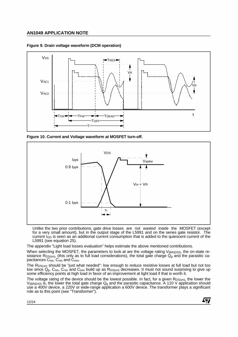
is possible to separate two different contributions to the total drain capacitance (CDrain): Coss, the in-ternal capacitance of the MOSFET, modulated by the drain voltage (manufacturers specify the value@ VDS = 25V), and CDext, the external parasitic capacitance due to the transformer and to the layoutof the circuit. In practice, it is possible to estimate CDrain from the drain voltage oscillation occuring af-ter the secondary current has run dry in DCM operation (see fig. 9). In fact, when the transformer isdischarged, the primary inductance starts resonating with CDrain and the oscillation period is:
TRES ≈ 2π ⋅ √Lp ⋅ CDrain (26). Turn-on losses depend on the input voltage in a non-monotonic way. As shown in fig. 9, the value of thedrain voltage at turn-on (VDon) in DCM operation is affected by the above mentioned oscillation. An inputvoltage increase, despite raising the settling value of the oscillation, may lead to a lower value at turn-onbecause of a particular combination of TON, TFW, TDEAD and TRES.
2 -Turn-off losses, due to the crossing of the active region that causes a voltage-current overlapping, asshown schematically in figure 10. The fall time (Tf) of a given MOSFET depends on the driver capa-bility (1.6A peak) and can be controlled with a series resistor placed between pin 10 and the gate ofthe MOSFET. The parasitic inductances (basically, the one located between source and ground) limit the maximumdi/dt rate achievable. The rate of rise of VDS depends mainly on CDrain.
3 - Gate drive losses, related to the charge to be delivered to the gate each time the MOSFET is turned on.This charge, supplied at fSB rate, results in an equivalent DC current IGD. The parameter to be consid-ered is the total gate charge (Qg) of the device, evaluated at the gate voltage delivered by the L5991.
AN1049 APPLICATION NOTE
11/24
Unlike the two prior contributions, gate drive losses are not wasted inside the MOSFET (exceptfor a very small amount), but in the output stage of the L5991 and on the series gate resistor. Thecurrent IGD is seen as an additional current consumption that is added to the quiescent current of theL5991 (see equation 25).
The appendix "Light load losses evaluation" helps estimate the above mentioned contributions.When selecting the MOSFET, the parameters to look at are the voltage rating V(BR)DSS, the on-state re-sistance RDS(on), (this only as to full load considerations), the total gate charge Qg and the parasitic ca-pacitances Ciss, Crss and Coss. The RDS(on) should be "just what needed": low enough to reduce resistive losses at full load but not toolow since Qg, Ciss, Crss and Coss build up as RDS(on) decreases. It must not sound surprising to give upsome efficiency points at high load in favor of an improvement at light load if that is worth it.The voltage rating of the device should be the lowest possible. In fact, for a given RDS(on), the lower theV(BR)DSS is, the lower the total gate charge Qg and the parasitic capacitance. A 110 V application shoulduse a 400V device, a 220V or wide-range application a 600V device. The transformer plays a significantrole as to this point (see "Transformer").
VAC1
t
VDS
TFW
TOFF
T
TON TDEAD
VAC2
VR
VR
TRES
Figure 9. Drain voltage waveform (DCM operation)
Ippk
VDS
0.9 Ippk
0.1 Ippk
Tf
Vin + VR
Vspike
Figure 10. Current and Voltage waveform at MOSFET turn-off.
AN1049 APPLICATION NOTE
12/24

Last, but not least significant, the technology. A good technology device offers lower gate charge andparasitic capacitances with the same V(BR)DSS, and RDS(on).
Transformer.The design and the assembly of the transformer plays a significant role in the process of power lossesminimization. The most annoying parasitic is the so-called "leakage inductance", that represents thestray primary magnetic flux, modeled as an inductor in series with the primary and not coupled to thesecondary. The energy stored in the leakage inductance produces an overvoltage spike on the drain ofthe MOSFET at turn-off. An external circuit will be necessary to clamp this spike so that the voltage rat-ing of the MOSFET is never exceeded.Therefore, when designing and building a transformer with the aim of optimizing the efficiency of theconverter at light load, the priorities are basically three:a) make the leakage inductance as low as possible. In terms of efficiency, there is a double noxious ef-
fect due to the leakage inductance. It not only dumps its own energy into the clamp circuit but alsodelays energy transfer from primary to secondary, after MOSFET turn-off, until it has run out of en-ergy. The result is that the energy stored in the mutual inductance is not completely transferred to thesecondary and is partly diverted into the clamp circuit and partly dissipated in the resistance of theprimary winding. This inefficiency is worsened by a light load and a high input voltage: both reducethe primary peak current and also the voltage across the leakage inductance (the leakage inductancespike) that resets the inductance itself. The lower this voltage is, the more energy transfer is delayedand the less energy is brought to the secondary.In practice, besides improving the energy transfer, a low leakage inductance will allow to lighten theaction of the external clamp and/or to select a lower voltage rating MOSFET. This will be beneficial toefficiency at heavy load as well.In order for a transformer to meet isolation and safety regulations, primary and secondary windingsmust be separated by isolation layers, thus their coupling cannot be intimate. As a result, it is not pos-sible to reduce leakage inductance below a certain extent. Practically, for a well assembled trans-former, leakage inductance will be about 1÷3% of the primary inductance.
Interleaved windings technique (putting on half the primary turns first, then all the secondaries and fi-nally the other half of the primary; see fig. 11) can reduce leakage inductance by 50%. The two pri-mary halves must be series connected, never paralleled. In general, multifilar winding technique (twisting the wire of two or more windings together) givesmaximum coupling between windings. In off-line converters, however, this technique is usually appli-cable only to secondary windings to get good cross-regulation, in case of multiple output. When multi-filar winding technique is not practicable because of very different turns number (or wire size), thesecondary winding with the highest output power should be wound closest to the primary; for thesame power the lowest voltage should be given priority.Other tricks, such as spacing windings evenly across a layer (when they do not completely fill it), orusing multiple strands of wire, or keeping isolation between windings to a minimum are also effective
1/2 primary turns
1/2 primary turns
secondary turns
air gap oncentre leg
Figure 11. Interleaved winding technique
AN1049 APPLICATION NOTE
13/24

to minimise leakage inductance.Also core and coil former geometry play an important role. To achieve good coupling, windings mustbe long and thin, and set out in concentric fashion. Therefore geometries with short and thick win-dows (such as RM, PQ or pot cores) should be avoided while ETD, EFD, EC and the majority of Ecores are good. Furthermore, it is not recommended to use split coil formers, where windings are ar-ranged side by side.
b) make the primary intrawinding capacitance as low as possible. This is the major component of theCDext capacitance earlier mentioned (see "MOSFET"). Besides contributing to MOSFET’s powerlosses, it causes ringing and noise problems that may force the use of additional damping networksto comply with EMC requirements. To achieve a low capacitance, always wind first the primary winding and, in particular, the half whoseend is to be connected to the drain of the MOSFET. In this way the second half primary has a shield-ing effect that reduces the capacitive coupling. In case of multiple layer windings, which exhibit highercapacitance, it is useful to embed one layer of isolation in between. This, however, tends to increaseleakage inductance and therefore should be done with care. Split coil formers are effective to this endbut, as mentioned earlier, degrade leakage inductance and then should be avoided.
c) make the reflected voltage low. As a rule of thumb, it should be below 60V in 110 VAC applicationsand less than 100V in 220 VAC or wide-range mains applications. This will reduce the voltage on thedrain of the MOSFET during its OFF-time and the losses on the resistor of the clamp network (if anRCD type is used, see "Clamp network"). Besides, a lower reflected voltage often leads to a primary-to-secondary turns ratio closer to 1:1. A positive side effect of that is a better magnetic coupling be-tween windings, which, in turn, helps reduce leakage inductance. On the other hand, consider that alower reflected voltage involves higher primary peak currents at heavy load.
Clamp network. Typically, the voltage spike due to transformer’s leakage inductance is limited by an RCD clamp (see fig.12a). Its action should be very light so as to have a spike as large as possible, consistently with the needof never exceeding the voltage rating of the MOSFET. This will optimize energy transfer from primary tosecondary. A low leakage inductance of the transformer is, of course, extremely helpful.RCD clamps dissipate power even under no-load conditions: there is always the reflected voltage acrossthe clamp resistor (R). To reduce clamp losses to a negligible level at light load, the use of a zenerclamp (see fig. 12b) is recommended whenever possible. Such a circuit gives also a well defined clamp-ing level but, on the other hand, dissipates more power at full load. Its use is therefore limited to lowpower applications.An alternative to these solutions can be the use of a non-dissipative clamp like the LCD one shown infig. 12c, which helps also reduce turn-off losses in the MOSFET. This circuit recovers the majority of theleakage inductance energy by transferring it back onto the input voltage rail through C and D2. There isjust a little power dissipation on the two diodes and the inductor. However, there is a slight increase ofthe conduction losses in the MOSFET at heavy load and, besides, the circuit is quite expensive and noteasy to optimise.
RC
D
RCD CLAMP
D
ZENERCLAMP
DZ
D1
LCD CLAMP
D2
L
C
a) b) b)
Figure 12. Possible clamp circuit topologies.
AN1049 APPLICATION NOTE
14/24

Whatever the clamp circuit topology is, the selection of the components is not trivial but needs specialcare to avoid annoying problems. The capacitors should be low-loss type (with polypropylene or polystyrene film dielectric) to reducepower dissipation and prevent overheating due to the high peak currents they experience.The blocking diodes must be not only very fast-recovery but also very fast-turn-on type. They should berated for repetitive peak currents greater than Ippk and their voltage rating must be adequate but notmuch higher than necessary. For a given diode type, the higher its breakdown voltage is, the longer itsturn-on time will be. This leads to higher turn-on losses and larger overvoltage spikes, extending abovethe clamp level, on the MOSFET’s drain.The zener diode must have an adequate power handling capability in both transient and steady state op-eration. The zener voltage should be approximately 50% higher than the reflected voltage so as not tohave too high power dissipation at heavy load. A transient voltage suppressor (Transil) can be effectivelyused in place of zener diodes. Table 4 lists some recommended devices available from ST: BZV and1N53xx types are zener diodes, all the others are Transil. SM15Txx devices are for surface mount as-semblies.
Table 4 - Recommended ST’s devices for clamping
Power handling capability (steady state)
Reflected voltage 1.7W 2.0W 5.0W 6.5W 10.0W
VR ≤ 50V BZW04-70BZW06-70
BZV47C68 P6KE68A1.5KE68A
BZW50-68 SM15T68A
VR ≤ 100V BZW04-128BZW06-128
BZV47C150 P6KE150A1.5KE150A1N5383B
BZW50-150 SM15T150A
Miscellaneous. There are some other hidden losses that can be significant under light load conditions and that could beworth reducing. At least, the designer should be aware of them.- Dummy load. Sometimes a minimum load current is required to maintain regulation and to prevent the
output voltage from drifting high. A ballast resistor capable of sinking this minimum amount of currentis usually placed at the output, so that the external load can be disconnected without any output volt-age drift. Obviously, this resistor dissipates a constant amount of power that degrades efficiency, es-pecially at light load, and should be removed if possible or at least minimized. The frequency reduc-tion offered by the L5991 helps to this end.
- Feedback. The resistor divider of the feedback network (including typically an optocoupler with a volt-age reference/error amplifier like the TL431) absorbs some mA, thus representing a dummy load thatadds to the actual one. If possible, the feedback network should be connected to the lowest outputvoltage of the converter.
- Residual resistive losses. Although currents involved at light load are very low, some residual "RI2 "losses are still present. They are mainly located in the bridge rectifier, in the inrush current limiter, inthe output steering diode and in the transformer, both as ohmic losses and radiation losses. Consideralso that the converter is drawing very little input (real) power but much higher (up to 4-5 times) ap-parent power and that the RMS currents circulating upstream the input bulk capacitor are related tothe apparent power.
- Case-to-heatsink parasitic capacitor. Due to the capacitive coupling of the MOSFET’s package (typi-cally, 15-20 pF for a TO220 case) to the heatsink (which is grounded for RFI reasons), current is by-passed from the drain to ground. This current does not usually generate heat but represents adummy load. If necessary, it is possible to minimize this loss by interposing a separator, between thepackage and the heatsink, made up of an insulating material with a metal foil embedded in it. Thishalves the capacitance and therefore the current. Moreover, the foil may be a point from which a littleenergy can be drawn for biasing some low consumption circuit.
- RC damping networks. They are commonly used to damp ringings that generate EMI and may be lo-cated at both the primary and the secondary side. Damping is inherently dissipative, hence these RCnetworks should be removed. Reduction of switching speed of the MOSFET, careful PCB layout, ap-propriate transformer construction and selection of EMI filter components may make damping unnec-essary.
AN1049 APPLICATION NOTE
15/24

Experimental results In order to validate the above considerations, an experimental example will be given. It concerns a 40W,wide-range mains power supply for an inkjet printer, whose design has been optimized following some ofthe guidelines here presented, and evaluated on the bench.Fig. 13 shows the schematic with indication of the relevant parts. The 28V output powers the steppermotors while the 12V output supplies the printhead. When the printer is idle these two outputs are notloaded. The 5V section supplies the logic circuits as well as the µcontroller that must be operating alsowhen the system is idle.The system operates at 100 kHz at nominal load. This value is set by the parallel of the 22 kΩ and the5.6 kΩ resistors connected at pin 2, along with the 3.3 nF capacitor placed between pin 2 and ground.When the output load is decreased so that the input power falls below about 8W, the output of the erroramplifier crosses the lower threshold (VT1) of the internal comparator. The L5991 now disconnects inter-nally the 5.6 kΩ resistor, so that the capacitor is charged through the 22 kΩ resistor only and the oscilla-tor frequency is changed to about 20 kHz.
The system works in standby at 20 kHz as long as the input power does not exceed about 9 W. Whenthe load current increases and this power is exceeded, the output of the error amplifier overcomes theupper threshold (VT2) and the L5991 connects again the 5.6kΩ resistor, thus switching the oscillator fre-quency back to 100 kHz.
4700pF 4KV 4700pF 4KV
4.7M
STP4NA60
4N35
220
2 x 330µF35V
1K
0.022µF
2.7K
3.9K
28V / 0.7A
GND
470µF 16V
BYW100-50
BYW98-100
BYW100-2004.7M
12V / 1.5A
5V / 0.5A
C02 C01
F01 AC 250V T1A
85 to265 Vac
BD01
2.2LF01
56K
10 22
13 1K
12470pF
11
0.471/2 W
33 µF / 25V
891415
22
330K47K
2
3
4
1
0.1µF
22K
3.3 nF 16
7
330 nF
470
470pF
6
BAT46
TL431
L5991
STTA106
5
5.6K
N1
N2
N3
N4Naux
5.6K
5.6K
2 x 470µF16V
5.1K 270K
100µF400V
BZW50-100
1N4148 56K
Figure 13. 40W Power Supply for inkjet printers. Electrical schematic
TRANSFORMER SPECS.
CORE: EDT29x16x10, 3c85 material, 1.4mm air gapPrim. Induct: 260µHN1: 51 T, AWG26N2: 11 T, AWG25N3: 10 T, AWG20N4: 4 T, AWG25Naux: 10 T, AWG32
AN1049 APPLICATION NOTE
16/24

The target was to draw from the line less than 2W over the entire input voltage range with the 28V and12V outputs unloaded and with the minimum load (0.55 W) on the 5V section. The results of the evalu-ation are summarized in table 5.
Table 5. 40W Power Supply for inkjet printer. Standby consumption.
Mains Voltage 85Vac 110Vac 160Vac 220Vac 265Vac
Input Power 0.93W 0.97W 1.13W 1.34W 1.87W
Input Power (*) 0.90W 0.93W 1.03W 1.14W 1.57W
Output Power 0.55W
(*) By using start-up circuit of fig. 7c.
APPENDIXFlyback BasicsFlyback’s operation takes place in a two-step process. During the ON time of the switch, energy is takenfrom the input and stored in the primary of the flyback transformer (actually, two coupled inductors). Atthe secondary side, the catch diode is reverse-biased, thus the load is being supplied by the energystored in the output bulk capacitor.
Vout
VOLTAGEREFERENCE
Vin
CLOCK
LATCH
R
S
Q
Rs
DRIVER
-
+
ERRORAMPLIFIER
-
+ 2R
R1V
PWMCOMPARATOR
ISOLATEDFEEDBACK
Ip
Lp
Vcs
VcVCOMP
Vc/3
Is
Vdrain
Vac
CONTROLLER
Q
CLOCK
VC/3
Vcs=Ip•Rs
Is
VdrainVin
n•Vout
DCM operation
Q
CLOCK
VC/3
Vcs=Ip•Rs
Is
Vdrain
∆Ip
CCM operation
Q
CLOCK
VC/3
Vcs=Ip•Rs
Is
Vdrain
TRANSITION
Figure A1. Flyback Topology with peak current mode control and associated waveforms
AN1049 APPLICATION NOTE
17/24

When the switch turns off, the primary circuit is open and the energy stored in the primary is transferredto the secondary by magnetic coupling. The catch diode is forward-biased, and the energy is deliveredto the output capacitor and to the load (recirculation). The output voltage is reflected back to the primarythrough the turns ratio and adds up to the input voltage (typically, the filtered rectified mains), giving ori-gin to a much higher voltage on the drain of the MOSFET.Flyback topology is operating in DCM (Discontinuous Conduction Mode) when the input -or primary -current starts from zero at the beginning of a given switching cycle. This happens because the secon-dary of the transformer has discharged all the energy stored in the previous period. If this energy trans-fer is not complete, then the primary current will start from a value greater than zero at the beginning ofeach cycle. Then the flyback is said to be operating in CCM (Continuous Conduction Mode). DCM ischaracterized by currents shaped in a triangular fashion, whereas CCM features trapezoidal currents(see fig. A1).The boundary between these two types of operation depends on several parameters. Some of them arestructural, that is parameters that identify the flyback converter: inductance of the primary of the trans-former, transformer turns ratio and regulated output voltage. Others are related to the external world andare subject to changes: input voltage and output load. The switching frequency is usually a structural pa-rameter, unless it is synchronized to an external signal.As to flyback topology operating in DCM, the relationship between the peak input current (Ippk) and theinput power (Pin) is:
Ippk(DCM) = √2 ⋅ Pin
Lp ⋅ fsw (A1).
where Lp is the inductance of the primary of the transformer and fsw the switching frequency. The point is: in a given flyback, when operating in DCM, the peak input current depends solely on thepower drawn from the input.The conduction time (TON, during which the MOSFET is ON) and the recirculation time (TFW, duringwhich the MOSFET is OFF and the catch diode is conducting) are respectively:
TON = Lp ⋅ Ippk(DCM)
Vin ; TFW = Lp ⋅
Ippk(DCM)
n ⋅ (Vout + VF) (A2)
where Vin is the DC input voltage and n the primary-to-secondary turns ratio, Vout the regulated outputvoltage and VF the forward drop across the catch diode.The quantity n • (Vout + VF) is the voltage reflected back to the primary during the recirculation at thesecondary. In the following will be indicated with VR:
VR = n ⋅ (Vout + VF) (A3).
Under the assumption of DCM, the sum of TON and TFW is less than the switching period T=1 / fsw. Thetransition between DCM and CCM implies:
TON + TFW = T (A4)
and, by combining equations (A1), (A2), (A3) in (A4), it is possible to determine the "Transition Power"(PinT), that is the maximum input power at which a given flyback works in DCM (or rather the minimuminput power at which it works in CCM) for a given input voltage (and a given switching frequency, if thiscan vary):
PinT = 1
2 ⋅ fsw ⋅ Lp ⋅
Vin
1 + Vin
VR
2
(A5);
AN1049 APPLICATION NOTE
18/24

obviously, DCM will take place for Pin < PinT andCCM for Pin > PinT. This equation can be rewrittenas follows:
PinT = VE
2
2 ⋅ ZE (A6)
by defining the "Equivalent Input Voltage" (VE) andthe "Equivalent Primary Impedance" (ZE):
VE = Vin
1 + Vin
VR
; ZE = fSW ⋅ Lp (A7).
VE is a function of Vin only (see fig. A2), since thereflected voltage (VR) is fixed. The variation of VE inits range [VEmin , VEmax ], which depends on themains voltage range, in turn defines the range ofPinT [PinTmin ,PinTmax].
Fig. A3 shows the diagram of (A6) while Tab. A1presents the ranges of VE relevant to typical mainsvoltage ranges, as well as the correspondingPinTmax / PinTmin ratios.To complete the characterization of the transitionbetween DCM and CCM it is convenient to definethe Transition Voltage (VET), that is the EquivalentInput Voltage at which the operation is on theboundary between DCM and CCM, for a given Pinand a given ZE:
VET = √2 ⋅ ZE ⋅ Pin (A8).
DCM will take place for VE > VET and CCM for VE <VET. In synchronized converters it is possible to definealso the Transition Frequency (fT), that is the switch-ing frequency at which the operation is on theboundary between DCM and CCM, for a given VE and a given Pin:
fT = VE
2
2 ⋅ Lp ⋅ Pin (A9).
DCM will take place for fsw < fT and CCM for fsw > fT.The peak primary current at transition is then:
Ippk(T) = √2 ⋅ PinT
fSW ⋅ Lp =
1fSW ⋅ Lp
⋅ Vin
1 + Vin
VR
= VE
ZE (A9).
In case of CCM operation, equation (A4) still applies but the timing relationships (A2) change as follows:
TON = Lp ⋅ ∆Ip
Vin ; TFW = T − TON =
Lp ⋅ ∆IpVR
(A10),
where ∆Ip is the primary current ripple.
n• Vout
VE
Vinmin Vinmax
VEmax
VEmin
Vin
Figure A2. Equivalent Input Voltage vs. DCInput Voltage
VE
PinT
VEmin VEmax
Pin
VET
fsw
Figure A3. Characterization of the transi-tion DCM ⇐⇒ CCM
AN1049 APPLICATION NOTE
19/24

Table A1. Typical V E ranges
Mains 110Vac ± 20% 220/240 Vac ± 20% Universal
Vin 100 ÷ 175Vdc 215 ÷ 370Vdc 100 ÷ 400Vdc
VE PinTmax/PinTmin VEPinTmax/P inTmin VE PinTmax/PinTmin
VR = 50V 33.3 ÷ 38.9 1.37 40.6 ÷ 44.0 1.18 33.3 ÷ 44.4 1.78
VR = 100V 50.0 ÷ 63.6 1.62 68.3 ÷ 78.7 1.33 50.0 ÷ 80.0 2.56
VR = 150V 60.0 ÷ 80.8 1.81 88.4 ÷ 106.7 1.46 60.0 ÷ 109.1 3.31
The peak primary current is no more uniquely related to Pin but now depends also on VE (i.e. Vin):
Ippk(CCM) = Pin
Vin ⋅ T
TON +
12
⋅ ∆Ip = Pin
VE +
VE
2 ⋅ ZE (A11).
It is possible to prove that Ippk is minimum when VE = VET for a given Pin (>PinTmin), that is at the transi-tion, then it will be maximum for VE = VEmin (i.e. for Vin = Vinmin).It is convenient to classify flyback converters on the basis of their maximum input power Pinmax:
Pinmax = Poutmax + Pextra
η (A12),
being Poutmax their rated output power, Pextra some extra output power provided for transients or tempo-rary overloads and η their efficiency, as follows:
Pinmax < PinTmin (⇒ VET < VEmin): DCM flyback;PinTmin < Pinmax < PinTmax (⇒ VEmin < VET < VEmax): MCM (Mixed Conduction Mode) flyback ;Pinmax > PinTmax (⇒ VET > VEmax): CCM flyback.
Peak Current Mode Control BasicsThe following relationships describing the "peak" current mode control are based on the architectureshown in fig. A1 and implemented by the L5991.From the inspection of the schematic of fig. A1 it is possible to find the relationship between the peak pri-mary current (Ippk), the peak voltage (Vcspk) on the (-) input of the PWM comparator and the output volt-age (VCOMP) of the error amplifier (E/A):
VCOMP = VC + 2 ⋅ Vf = 3 ⋅ Vcspk + 2 ⋅ Vf = 3 ⋅ (Rs ⋅ Ippk + Vo) + 2 ⋅ Vf (B1)
where Vf is the forward drop on each "zero duty cycle diode" (0.7V typ.) and Vo a DC offset voltage thatmay be applied on the (-) input of the PWM comparator (that is on the current sense pin of the L5991).VC, the voltage downstream the two zero duty cycle diodes (and applied on the x3 divider), despite notreally available, can be considered for convenience.Considering the 1V clamp on the (+) input of the current sense comparator, VC will be included between0 and 3 V, and the useful swing of VCOMP between 2 ⋅ Vf and 3 + 2 ⋅ Vf volt.Actually, equation (B1) neglects the so-called "delay to output" of the PWM controller, that is the propa-gation delay of the current sense path (PWM comparator + latch + driver). During this time, the switch isstill ON and the input current keeps on ramping up, despite Vcs has already hit the internal level on (-)input of the PWM comparator.This time lag (TDELAY, 70 ns typ. 100 ns max.) is compensated by the voltage loop when the system isregulating: VCOMP is slightly lower than the value predicted by (B1) but the phase margin of the controlloop gain gets less. Instead, when the error amplifier is saturated high and the pulse-by-pulse limiting istripped, TDELAY causes the peak current Ippk to be larger than the expected limit 1 / Rs. As illustrated infig. B1, the effect is more pronunciated as the input voltage increases.
AN1049 APPLICATION NOTE
20/24

To account for delay to output, equation (B1) should be rewritten as follows:
VCOMP = 3 ⋅ [Rs ⋅ (Ippk − ∆I) + Vo] +2 ⋅ Vf (B2),
where the current overflow ∆I is:
∆I = Vin
Lp ⋅ TDELAY (B3).
If the offset voltage is selected so that:
Vo = V’o = Rs ⋅ ∆I = Rs ⋅ Vin
Lp ⋅ TDELAY (B4),
the term ∆I and Vo in (B1) will cancel one the otherand the effect of the delay to output is eliminated.Equation (B1) will still apply, provided Vo is re-garded as the difference between the actual voltageapplied on the current sense pin of the L5991 andthe compensating value V’o. The compensation can be easily realized with thecircuit shown in fig. B2. R2 is often used along withthe capacitor C to smooth the leading edge spikesoccurring when the switch turns on. In such a caseonly R1 will be added. Considering that V’o is in the hundred mV or less andthat, therefore, R1 >> R2 (R2 is typically 1kΩ, R1 willbe in the MΩ), perfect delay compensation will beachieved when the ratio of the two resistors is:
R2R1
= Rs ⋅ TDELAY
Lp (B5).
The resistor R3, connected to the 5V reference volt-age externally available on pin 4, is used for addi-tional offsetting the voltage on the current sensepin.
TDELAY
VCOMP-2·Vf3 Rs
∆Imin∆Imax
Vin = Vinmin Vin = Vinmax
Ipx
Vomin
Vomax
Vcs
VCOMP -2·Vf3
Vin = Vinmin Vin = Vinmax
VCLAMP
3
VCLAMP
3
a) b)
Figure B1. Effect of the delay to output (a) and its compensation by means of Vo (b)
Vin
Rs
L5991R2
R1
C
Vref
R3
410
1312
Figure B2. Compensation of the delay to out-put.
AN1049 APPLICATION NOTE
21/24

Light load losses evaluationHere follows a number of relationships useful to evaluate the major losses in a lightly loaded flyback.
Table C1 - Start-up circuits of fig. 7a and 7b
Maximum R START PSTARTmax Maximum Wake-up time
Circuit a) 1.41 ⋅ VACmin − VTH
ISTART
(1.41 ⋅ VACmax − VCC)2
RSTART≈ CSUPPLY ⋅
2 ⋅ VTH ⋅ RSTART
3 ⋅ VACmin − VTH − ISTART ⋅ RSTART
Circuit b)0.45 ⋅ VACmin −
12
⋅ VTH
ISTART
VACmax ⋅ (VACmax − 1.35 ⋅ VCC)2 ⋅ RSTART
≈ CSUPPLY ⋅ 2 ⋅ VTH ⋅ RSTART
VACmin − VTH − ISTART ⋅ RSTART
Worst case values: VTH = 16V, I START = 120µAVCC is the supply voltage delivered by the self-supply circuit
Table C2 - MOSFET losses (refer to fig. 10)
Turn-on losses Turn-off losses Gate-drive current (IGD) Equivalent Drain Capacitance
≈ 12
⋅ CDrain ⋅ VDon2 ⋅ fSB ≈
Ippk2 ⋅ Tf
2 ⋅ fSB
6 ⋅ CDrainQg ⋅ fSB ≈
TRES2
4π2 ⋅ Lp
Table C3. Clamp network losses (refer to fig. 12)
RCD Zener or Transil LCD
≈VR
2
R≈ 0 ≈ 0
AN1049 APPLICATION NOTE
22/24

SUMMARY
Page
INTRODUCTION 1
The L5991 .......................................................................................................................... 2
Standby Function Description............................................................................................. 3
Standby Operation Analysis ............................................................................................... 4
Standby Function Setup ..................................................................................................... 7
Standby Function and Error................................................................................................ 8
OPTIMISING THE DESIGN FOR MAXIMUM EFFICIENCY AT LIGHT LOAD
Start-up & Self-supply Circuits............................................................................................ 8
Power MOSFET ................................................................................................................. 11
Transformer ........................................................................................................................ 13
Clamp Network ................................................................................................................... 14
Miscellaneous..................................................................................................................... 15
Experimental Results.......................................................................................................... 16
APPENDIX
Flyback Basics.................................................................................................................... 17
Peak Current Mode Control Basics .................................................................................... 20
Light Load Losses Evaluation............................................................................................. 22
AN1049 APPLICATION NOTE
23/24

Information furnished is believed to be accurate and reliable. However, STMicroelectronics assumes no responsibility for the consequencesof use of such information nor for any infringement of patents or other rights of third parties which may result from its use. No license isgranted by implication or otherwise under any patent or patent rights of STMicroelectronics. Specification mentioned in this publication aresubject to change without notice. This publication supersedes and replaces all information previously supplied. STMicroelectronics productsare not authorized for use as critical components in life support devices or systems without express written approval of STMicroelectronics.
The ST logo is a registered trademark of STMicroelectronics© 2000 STMicroelectronics – Printed in Italy – All Rights Reserved
STMicroelectronics GROUP OF COMPANIESAustralia - Brazil - China - Finland - France - Germany - Hong Kong - India - Italy - Japan - Malaysia - Malta - Morocco -
Singapore - Spain - Sweden - Switzerland - United Kingdom - U.S.A.http://www.st.com
AN1049 APPLICATION NOTE
24/24