MicrowaveClass-F and Inverse Class-F Power Amplifiers...
4
Proceedings of the 36th European Microwave Conference Microwave Class-F and Inverse Class-F Power Amplifiers Designs using GaN Technology and GaAs pHEMT S. Gaol, P. Butterworth', A. Sambell', C. Sanabria2, H. Xu2, S. Heikman2, U. Mishra2 and R. A. York2 'Active Antenna Group, School of Engineering, University of Northumbria, Newcastle Upon Tyne NEI 8ST, UK Tel: 44-191-2274566 Email: shichang.gao(k4unn.ac.uk 2Electrical and Computer Engineering Department, University of California, Santa Barbara, CA 93106, USA ABSTRACT - This paper presents the designs and results of two high-efficiency harmonics-tuned microwave power amplifiers (PA): the first one is a 2 GHz class-F PA in monolithic integrated circuit (MMIC) by using GaN HEMT technology, and the other one is a 2.45-GHz inverse class-F PA using packaged GaAs pHEMT devices with PCB technology. In the class-F MMIC PA, field-plated GaN HEMT device is used for high-power performance. The 2.0- GHz class-F MMIC PA achieves a PAE of 50%, 38 dBm output power, and 6.2 W/mm power density. The inverse class-F PA at 2.45 GHz achieves 22.6 dBm output power and 73% PAE at 3 dB compression, and has very low cost. Index Terms - Power amplifiers, high efficiency, class F, inverse class-F, MMIC, GaN HEMT, GaAs I. INTRODUCTION Radio frequency (RF) and microwave PA is the most expensive component in radio transmitters of modern communications and radar systems. A high PAE is one of the key requirements in RF/microwave PA designs, as it will lead to low power consumption, reduced cooling requirements, small battery size and low cost in RF front ends. To achieve a high PAE, it is necessary to drive the active device heavily into compression, leading to highly non-linear behaviour. Popular design techniques include those based on harmonic manipulation such as Class-F and Inverse Class-F [1,2], or switching mode such as Class-E [3,4], etc. The characteristics of these different high-efficiency modes are best appreciated by observing the shape of the voltage and current waveforms at the output of the active device. In contrast to the old days when the class-F PA designers focused on the harmonics tuning at the output only, many recent work on class-F and inverse class-F PAs have shown the importance of considering the harmonics tuning at both the input and the output. For example, the 2nd harmonic input termination has been shown experimentally to have a significant influence on efficiency and linearity [2,5], demonstrating the need to integrate it into the design process. Many work on harmonics-tuned PA have been reported by using GaAs devices for class-F PA in MMIC or hybrid circuits [6-10], and SiGe HBT for MMIC class-F PA [11], etc. This paper presents the design and results of two high- efficiency PAs: one is a 2 GHz class-F MMIC PA by using GaN HEMT technology, and the other one is a very low cost inverse class-F PA at 2.45 GHz which uses packaged GaAs pHEMT devices and printed circuit board (PCB) technology. A multi-harmonics source pull/load pull simulation-based design methodology is employed. II. PRINCIPLES OF CLASS-F AND INVERSE CLASS- F PA AND DESIGN METHDOLOGY A. Class-F and inverse class-F PA Basics The class-F PA achieves high efficiency and high output power by using harmonic resonators in its output network to shape the drain waveforms in the time domain. Ideally, the load must be short at even harmonics and open at odd harymonics. The drain voltage waveform includes odd harymonics and approximates a square wave, while the drain current waveform includes even harmonics and approximates a half sine wave. In practical realizations of microwave class-F PA, only the first three harmonics are considered, as higher harmonics can be shorted by the output drain capacitance Cds. The input harmonics tuning is very important here as it plays an important role in shaping the driving waveform at the device input, and modifying the harymonic components at the device output, etc [6]. In the inverse class-F PA, the load must be short at odd harmonics and open at even harmonics. The drain current waveform includes odd harmonics and approximates a square wave, while the drain voltage waveform includes even harmonics and approximates a half sine wave. Again, up to the third harmonics are considered at both the input and the output networks. September 2006, Manchester UK 2-9600551-6-0 (D 2006 EuMA 1719 Authorized licensed use limited to: Univ of California-Santa Barbara. Downloaded on April 29, 2009 at 16:42 from IEEE Xplore. Restrictions apply.
Transcript of MicrowaveClass-F and Inverse Class-F Power Amplifiers...

Proceedings of the 36th European Microwave Conference
Microwave Class-F and Inverse Class-F Power Amplifiers Designsusing GaN Technology and GaAs pHEMT
S. Gaol, P. Butterworth', A. Sambell', C. Sanabria2, H. Xu2, S. Heikman2, U. Mishra2 and R. A. York2'Active Antenna Group,
School of Engineering, University of Northumbria,Newcastle Upon Tyne NEI 8ST, UK
Tel: 44-191-2274566Email: shichang.gao(k4unn.ac.uk
2Electrical and Computer Engineering Department,University of California, Santa Barbara, CA 93106, USA
ABSTRACT - This paper presents the designs andresults of two high-efficiency harmonics-tuned microwavepower amplifiers (PA): the first one is a 2 GHz class-F PA inmonolithic integrated circuit (MMIC) by using GaN HEMTtechnology, and the other one is a 2.45-GHz inverse class-FPA using packaged GaAs pHEMT devices with PCBtechnology. In the class-F MMIC PA, field-plated GaNHEMT device is used for high-power performance. The 2.0-GHz class-F MMIC PA achieves a PAE of 50%, 38 dBmoutput power, and 6.2 W/mm power density. The inverseclass-F PA at 2.45 GHz achieves 22.6 dBm output power and73% PAE at 3 dB compression, and has very low cost.
Index Terms - Power amplifiers, high efficiency, class F,inverse class-F, MMIC, GaN HEMT, GaAs
I. INTRODUCTION
Radio frequency (RF) and microwave PA is the mostexpensive component in radio transmitters of moderncommunications and radar systems. A high PAE is one ofthe key requirements in RF/microwave PA designs, as itwill lead to low power consumption, reduced coolingrequirements, small battery size and low cost in RF frontends. To achieve a high PAE, it is necessary to drive theactive device heavily into compression, leading to highlynon-linear behaviour. Popular design techniques includethose based on harmonic manipulation such as Class-Fand Inverse Class-F [1,2], or switching mode such asClass-E [3,4], etc. The characteristics of these differenthigh-efficiency modes are best appreciated by observingthe shape of the voltage and current waveforms at theoutput of the active device. In contrast to the old dayswhen the class-F PA designers focused on the harmonicstuning at the output only, many recent work on class-Fand inverse class-F PAs have shown the importance ofconsidering the harmonics tuning at both the input and theoutput. For example, the 2nd harmonic input terminationhas been shown experimentally to have a significantinfluence on efficiency and linearity [2,5], demonstrating
the need to integrate it into the design process. Many workon harmonics-tuned PA have been reported by usingGaAs devices for class-F PA in MMIC or hybrid circuits[6-10], and SiGe HBT for MMIC class-F PA [11], etc.This paper presents the design and results of two high-efficiency PAs: one is a 2 GHz class-F MMIC PA byusing GaN HEMT technology, and the other one is a verylow cost inverse class-F PA at 2.45 GHz which usespackaged GaAs pHEMT devices and printed circuit board(PCB) technology. A multi-harmonics source pull/loadpull simulation-based design methodology is employed.
II. PRINCIPLES OF CLASS-F AND INVERSE CLASS-F PA AND DESIGN METHDOLOGY
A. Class-F and inverse class-FPA BasicsThe class-F PA achieves high efficiency and high output
power by using harmonic resonators in its output networkto shape the drain waveforms in the time domain. Ideally,the load must be short at even harmonics and open at oddharymonics. The drain voltage waveform includes oddharymonics and approximates a square wave, while thedrain current waveform includes even harmonics andapproximates a half sine wave.
In practical realizations of microwave class-F PA, onlythe first three harmonics are considered, as higherharmonics can be shorted by the output drain capacitanceCds. The input harmonics tuning is very important here asit plays an important role in shaping the driving waveformat the device input, and modifying the harymoniccomponents at the device output, etc [6].
In the inverse class-F PA, the load must be short at oddharmonics and open at even harmonics. The drain currentwaveform includes odd harmonics and approximates asquare wave, while the drain voltage waveform includeseven harmonics and approximates a half sine wave.Again, up to the third harmonics are considered at boththe input and the output networks.
September 2006, Manchester UK2-9600551-6-0 (D 2006 EuMA 1719Authorized licensed use limited to: Univ of California-Santa Barbara. Downloaded on April 29, 2009 at 16:42 from IEEE Xplore. Restrictions apply.
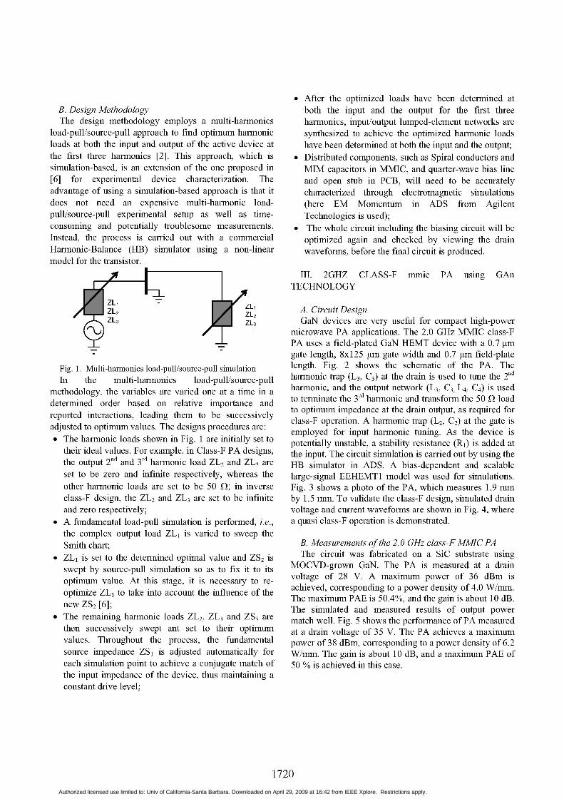
B. Design MethodologyThe design methodology employs a multi-harmonics
load-pull/source-pull approach to find optimum harmonicloads at both the input and output of the active device atthe first three harmonics [2]. This approach, which issimulation-based, is an extension of the one proposed in[6] for experimental device characterization. Theadvantage of using a simulation-based approach is that itdoes not need an expensive multi-harmonic load-pull/source-pull experimental setup as well as time-consuming and potentially troublesome measurements.Instead, the process is carried out with a commercialHarmonic-Balance (HB) simulator using a non-linearmodel for the transistor.I~~
ZL2ZL3
_'I
ZL1ZL2ZL3
Fig. 1. Multi-harmonics load-pull/source-pull simulationIn the multi-harmonics load-pull/source-pull
methodology, the variables are varied one at a time in adetermined order based on relative importance andreported interactions, leading them to be successivelyadjusted to optimum values. The designs procedures are:* The harmonic loads shown in Fig. 1 are initially set to
their ideal values. For example, in Class-F PA designs,the output 2nd and 3rd harmonic load ZL2 and ZL3 areset to be zero and infinite respectively, whereas theother harmonic loads are set to be 50 Q; in inverseclass-F design, the ZL2 and ZL3 are set to be infiniteand zero respectively;
* A fundamental load-pull simulation is performed, i.e.,the complex output load ZLI is varied to sweep theSmith chart;
* ZLI is set to the determined optimal value and ZS2 isswept by source-pull simulation so as to fix it to itsoptimum value. At this stage, it is necessary to re-optimize ZLI to take into account the influence of thenew ZS2 [6];
* The remaining harmonic loads ZL2, ZL3 and ZS3 arethen successively swept ant set to their optimumvalues. Throughout the process, the fundamentalsource impedance ZS, is adjusted automatically foreach simulation point to achieve a conjugate match ofthe input impedance of the device, thus maintaining aconstant drive level;
* After the optimized loads have been determined atboth the input and the output for the first threeharmonics, input/output lumped-element networks aresynthesized to achieve the optimized harmonic loadshave been determined at both the input and the output;
* Distributed components, such as Spiral conductors andMIM capacitors in MMIC, and quarter-wave bias lineand open stub in PCB, will need to be accuratelycharacterized through electromagnetic simulations(here EM Momentum in ADS from AgilentTechnologies is used);
* The whole circuit including the biasing circuit will beoptimized again and checked by viewing the drainwaveforms, before the final circuit is produced.
III. 2GHZ CLASS-F mmic PA using GAnTECHNOLOGY
A. Circuit DesignGaN devices are very useful for compact high-power
microwave PA applications. The 2.0 GHz MMIC class-FPA uses a field-plated GaN HEMT device with a 0.7 pmgate length, 8x125 pm gate width and 0.7 pm field-platelength. Fig. 2 shows the schematic of the PA. Theharmonic trap (L3, C3) at the drain is used to tune the 2ndharmonic, and the output network (L3, C3, L4, C4) is usedto terminate the 3rd harmonic and transform the 50 Q loadto optimum impedance at the drain output, as required forclass-F operation. A harmonic trap (L2, C2) at the gate isemployed for input harmonic tuning. As the device ispotentially unstable, a stability resistance (RI) is added atthe input. The circuit simulation is carried out by using theHB simulator in ADS. A bias-dependent and scalablelarge-signal EEHEMT1 model was used for simulations.Fig. 3 shows a photo of the PA, which measures 1.9 mmby 1.5 mm. To validate the class-F design, simulated drainvoltage and current waveforms are shown in Fig. 4, wherea quasi class-F operation is demonstrated.
B. Measurements ofthe 2. 0 GHz class-F MMIC PAThe circuit was fabricated on a SiC substrate using
MOCVD-grown GaN. The PA is measured at a drainvoltage of 28 V. A maximum power of 36 dBm isachieved, corresponding to a power density of 4.0 W/mm.The maximum PAE is 50.4%, and the gain is about 10 dB.The simulated and measured results of output powermatch well. Fig. 5 shows the performance ofPA measuredat a drain voltage of 35 V. The PA achieves a maximumpower of 38 dBm, corresponding to a power density of 6.2W/mm. The gain is about 10 dB, and a maximum PAE of50 % is achieved in this case.
1720Authorized licensed use limited to: Univ of California-Santa Barbara. Downloaded on April 29, 2009 at 16:42 from IEEE Xplore. Restrictions apply.

Fig. 3. Photo of the chip ofPA
0.0 0.2 0.4 0.6
Time(nS)0.8
100
80
6060 s:s0)
40 0a)
20 CD
01.0
Fig. 4. Drain current and voltages waveforms
PAE
- - ain ---
U 1l20 22 244 26 28 30 32
Pin(dBm)
IV. LOW-COST 2.45 GHZ INVERSE CLASS-F PAUSING PACKAGED GAAS PHEMT IN PCBTECHNOLOGYA. Circuit Design
Rol~~~~~CddLg L t
T A | ECdl AAX
Fig. 6. Circuit configuration of the inverse class-F PA
Very low-cost RF PAs can be realized by using low-cost packaged devices and PCB technology. Here GaAspHEMT device ATF 34143 from Agilent Technologies isemployed because of its low cost and the availability of itsnonlinear model from the company's web site. The designis based on the multi-harmonics source-pull/load-pullsimulation, i.e., the input/output networks are optimized toachieve the desired harmonic loads up to the thirdharmonic frequency.
Fig. 6 shows the circuit topology, where the DCbiasing is done by using a quarter-wave line shorted by aRF bypass capacitor. Resistors are used in the gate biascircuit and on the gate for achieving the stability. A / 12open-circuited microstrip stub is used to control the 3rdharmonic at the output. The 2nd harmonics at the input andoutput are provided by adjusting the length of quarter-wave bias lines. To check the mode of PA operation, thevoltage and current waveforms at the drain output aresimulated by using ADS and shown in Fig. 7, whichconfirms the quasi inverse class-F mode of operation.50
40
30-u30>DmI--
2 0 0-0Ids(A)
10
4-
Vds(V)
Fig. 5. Power, gain and PAE results of 2.0 GHz PA with a
Vds of 35 V
Fig. 7. Simulated drain waveforms in time domain
1721
1.2 -
1.08
0.86- 0.6
a) 0.4-
, 0.20
.: 0.02
a -0.24
-0.4
50-
-40-
(D 30-
m 202
0~1-o 101
r
-n- e
ou A o u
' 1
Authorized licensed use limited to: Univ of California-Santa Barbara. Downloaded on April 29, 2009 at 16:42 from IEEE Xplore. Restrictions apply.
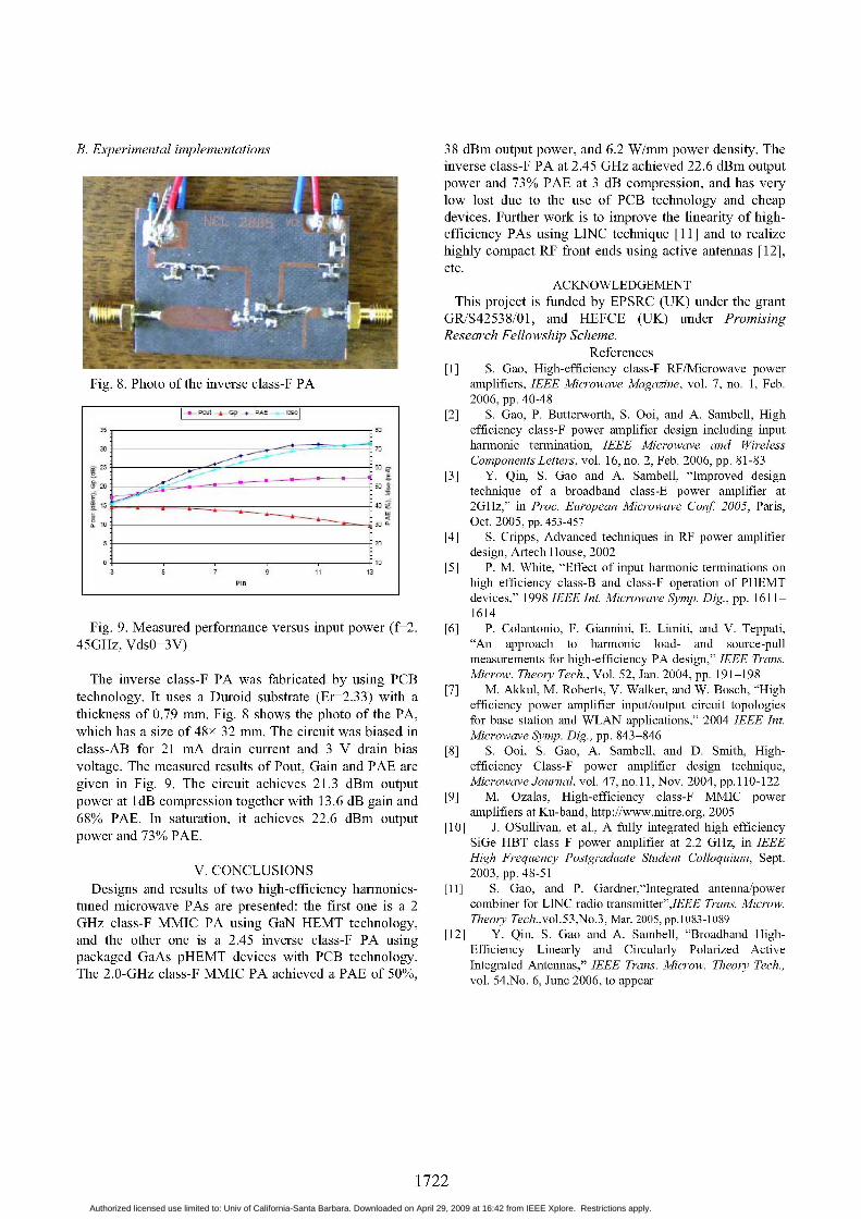
B. Experimental implementations
Fig. 8. Photo of the inverse class-F PA
Fig. 9. Measured performance versus input power (f=2.45GHz, VdsO=3V)
The inverse class-F PA was fabricated by using PCBtechnology. It uses a Duroid substrate (Er=2.33) with a
thickness of 0.79 mm. Fig. 8 shows the photo of the PA,which has a size of 48x 32 mm. The circuit was biased inclass-AB for 21 mA drain current and 3 V drain biasvoltage. The measured results of Pout, Gain and PAE are
given in Fig. 9. The circuit achieves 21.3 dBm outputpower at 1dB compression together with 13.6 dB gain and68% PAE. In saturation, it achieves 22.6 dBm outputpower and 73% PAE.
V. CONCLUSIONSDesigns and results of two high-efficiency harmonics-
tuned microwave PAs are presented: the first one is a 2GHz class-F MMIC PA using GaN HEMT technology,and the other one is a 2.45 inverse class-F PA usingpackaged GaAs pHEMT devices with PCB technology.The 2.0-GHz class-F MMIC PA achieved a PAE of 50%,
38 dBm output power, and 6.2 W/mm power density. Theinverse class-F PA at 2.45 GHz achieved 22.6 dBm outputpower and 73% PAE at 3 dB compression, and has verylow lost due to the use of PCB technology and cheapdevices. Further work is to improve the linearity of high-efficiency PAs using LINC technique [11] and to realizehighly compact RF front ends using active antennas [12],etc.
ACKNOWLEDGEMENTThis project is funded by EPSRC (UK) under the grant
GR/S42538/01, and HEFCE (UK) under PromisingResearch Fellowship Scheme.
References[1] S. Gao, High-efficiency class-F RF/Microwave power
amplifiers, IEEE Microwave Magazine, vol. 7, no. 1, Feb.2006, pp. 40-48
[2] S. Gao, P. Butterworth, S. Ooi, and A. Sambell, Highefficiency class-F power amplifier design including inputharmonic termination, IEEE Microwave and WirelessComponents Letters, vol. 16, no. 2, Feb. 2006, pp. 81-83
[3] Y. Qin, S. Gao and A. Sambell, "Improved designtechnique of a broadband class-E power amplifier at2GHz," in Proc. European Microwave Conf 2005, Paris,Oct. 2005, pp. 453-457
[4] S. Cripps, Advanced techniques in RF power amplifierdesign, Artech House, 2002
[5] P. M. White, "Effect of input harmonic terminations onhigh efficiency class-B and class-F operation of PHEMTdevices," 1998 IEEE Int. Microwave Symp. Dig., pp. 1611-1614
[6] P. Colantonio, F. Giannini, E. Limiti, and V. Teppati,"An approach to harmonic load- and source-pullmeasurements for high-efficiency PA design," IEEE Trans.Microw. Theory Tech., Vol. 52, Jan. 2004, pp. 191-198
[7] M. Akkul, M. Roberts, V. Walker, and W. Bosch, "Highefficiency power amplifier input/output circuit topologiesfor base station and WLAN applications," 2004 IEEE Int.Microwave Symp. Dig., pp. 843-846
[8] S. Ooi, S. Gao, A. Sambell, and D. Smith, High-efficiency Class-F power amplifier design technique,Microwave Journal, vol. 47, no.11, Nov. 2004, pp.110- 122
[9] M. Ozalas, High-efficiency class-F MMIC poweramplifiers at Ku-band, http://www.mitre.org, 2005
[10] J. OSullivan, et al., A fully integrated high efficiencySiGe HBT class F power amplifier at 2.2 GHz, in IEEEHigh Frequency Postgraduate Student Colloquium, Sept.2003, pp. 48-51
[11] S. Gao, and P. Gardner,"Integrated antenna/powercombiner for LINC radio transmitter",IEEE Trans. Microw.Theory Tech.,vol.53,No.3, Mar. 2005, pp.1083-1089
[12] Y. Qin, S. Gao and A. Sambell, "Broadband High-Efficiency Linearly and Circularly Polarized ActiveIntegrated Antennas," IEEE Trans. Microw. Theory Tech.,vol. 54,No. 6, June 2006, to appear
1722
-6- .d O 1.AE _. t
is~~~~~~~~~~~~~~~~~~~~~~s
10
1, Pin
. < .w.~~~~~~~lV-Wm
Authorized licensed use limited to: Univ of California-Santa Barbara. Downloaded on April 29, 2009 at 16:42 from IEEE Xplore. Restrictions apply.


![Rama's Defence - for web.ppt [Read-Only]my.ece.ucsb.edu/York/Yorklab/Projects/GaN/Defense/Rama's...Acknowledgements Professors Umesh Mishra, Robert York, Evelyn Hu, Dr. James Ibbetson](https://static.fdocuments.net/doc/165x107/5af6e5a77f8b9a9e5990050f/ramas-defence-for-webppt-read-onlymyeceucsbeduyorkyorklabprojectsgandefenseramasacknowledgements.jpg)