MICROSTRIP PATCH BALUN BANDPASS FILTEReprints.utar.edu.my/134/1/3E-2011-0704393-1.pdf · MICROSTRIP...
78
MICROSTRIP PATCH BALUN BANDPASS FILTER NG CHI HWA A project report submitted in partial fulfilment of the requirements for the award of the degree of Bachelor (Hons.) of Electrical and Electronics Engineering Faculty of Engineering and Science Universiti Tunku Abdul Rahman May 2011
Transcript of MICROSTRIP PATCH BALUN BANDPASS FILTEReprints.utar.edu.my/134/1/3E-2011-0704393-1.pdf · MICROSTRIP...
MICROSTRIP PATCH BALUN BANDPASS FILTER
NG CHI HWA
A project report submitted in partial fulfilment of the
requirements for the award of the degree of
Bachelor (Hons.) of Electrical and Electronics Engineering
Faculty of Engineering and Science
Universiti Tunku Abdul Rahman
May 2011

ii
DECLARATION
I hereby declare that this project report is based on my original work except for
citations and quotations which have been duly acknowledged. I also declare that it
has not been previously and concurrently submitted for any other degree or award at
UTAR or other institutions.
Signature : _________________________
Name : ______NG CHI HWA_______
ID No. : ______07UEB04393________
Date : ______15th April 2011_______

iii
APPROVAL FOR SUBMISSION
I certify that this project report entitled “MIRCROSTRIP PATCH BALUN
BANDPASS FILTER” was prepared by NG CHI HWA has met the required
standard for submission in partial fulfilment of the requirements for the award of
Bachelor of Electrical and Electronics Engineering (Hons.) at Universiti Tunku
Abdul Rahman.
Approved by,
Signature : _________________________
Supervisor : Dr. Lim Eng Hock
Date : ______15th April 2011_______
iv
The copyright of this report belongs to the author under the terms of the
copyright Act 1987 as qualified by Intellectual Property Policy of University Tunku
Abdul Rahman. Due acknowledgement shall always be made of the use of any
material contained in, or derived from, this report.
© 2011, Ng Chi Hwa. All right reserved.

v
Specially dedicated to
my beloved parents, coursemates and friends.

vi
ACKNOWLEDGEMENTS
I would like to thank everyone who had contributed to the successful completion of
this project. I would like to express my gratitude to my research supervisor, Dr. Lim
Eng Hock for his invaluable advice, guidance and enormous patience throughout the
development of the research.
In addition, I would also like to express my utmost gratitude to my loving
parents and friends who had helped and given me continuous supports throughout
this project.
vii
MICROSTRIP PATCH BALUN BANDPASS FILTER
ABSTRACT
Filtering is a very important process in our daily life. When it comes to
communication, filter is an essential component that is incorporated into the
communication device. Filter is used to eliminate unwanted frequencies or to select
desired range of frequencies. A new compact microstrip patch balun bandpass filter
has been proposed in this project and fabricated on RT/Duroid 6006 substrate. The
novelty of this design is that it divides the microwave signal equally into two with
1800 out of phase. The project can be separated into three major stages which are
simulation, fabrication and experimental stage. A series of simulations based on High
Frequency Structure Simulator (HFSS) will be run to simulate the filter design with
different configurations and the results are analysed. Frequency response of the
fabricated filter is measured by using Vector Network Analyzer (VNA) in laboratory.
Experiments have been conducted, with good agreement observed between the
simulated and measured results. The insertion loss, return loss and characteristic of
the each parameter is been studied. A thorough studies and further discussions have
been done on the proposed filter and recommendations have been proposed.

viii
TABLE OF CONTENTS
DECLARATION ii
APPROVAL FOR SUBMISSION iii
ACKNOWLEDGEMENTS vi
ABSTRACT vii
TABLE OF CONTENTS viii
LIST OF TABLES x
LIST OF FIGURES xi
LIST OF SYMBOLS / ABBREVIATIONS xvi
CHAPTER
1 INTRODUCTION 1
1.1 Background 1
1.2 Research Aims and Objectives 2
1.3 Project Motivation 3
2 LITERATURE REVIEW 4
2.1 About Microstrip Filter 4
2.1.1 Microstrip Lines 8
2.1.1.1 Dielectric Constant 9
2.1.1.2 Effective Dielectric Constant 10
2.1.1.3 Characteristic Impedance 12
2.1.2 Microstrip Resonators 13
2.1.2.1 Cross Slotted Patch Resonator 14
2.1.2.2 Circular Patch Resonator 18
2.1.2.3 Triangular Patch Resonator 20
2.2 Patch Filter 25
2.2.1 Applications of Patch Resonator 26
ix
2.2.2 Single-Mode Patch Filter 27
2.2.3 Dual-Mode Patch Filter 28
3 MICROSTRIP PATCH BALUN BANDPASS FILTER 33
3.1 Background 33
3.2 Research Methodology 35
3.2.1 Simulation Stage 35
3.2.2 Fabrication Stage 37
3.2.3 Experimental Stage 42
3.3 Proposed Filter Configurations 45
4 RESULTS AND DISCUSSIONS 47
4.1 Simulation and Experimental Results 47
4.2 Case Studies 51
4.2.1 Cross-slot Length 52
4.2.2 Cross-slot Width 53
4.2.3 Gap 55
4.2.4 Inclination Angle 57
5 CONCLUSION AND RECOMMENDATIONS 59
5.1 Conclusion 59
5.2 Recommendation 60
REFERENCES 61

x
LIST OF TABLES
TABLE TITLE PAGE
4.1 49
xi
LIST OF FIGURES
FIGURE TITLE PAGE
2.1 Microstrip filters linkage 5
2.2 Design of parallel couple microstrip lines bandpass
filter 6
2.3 Design of microstrip-fed dual-mode filter with
crossed slot and two triangular perturbation
elements at the center 6
2.4 Conventional design of triangular resonator dual-
mode filter 6
2.5 Dual-mode microstrip loop resonator design 7
1.6 Crossed slot microstrip rectangular patch bandpass
filter design 7
2.7 Circular patch bandpass filter with multi-order
harmonic suppressed I/O lines design 7
1.8 Three-pole microstrip semi-circular bandpass filter
design 8
1.9 Cross-section of microstrip geometry. 9
2.10 Substrate Figure 11
2.11 Geometry of two classes dual-mode planar filter
(a) Conventional type (b) Novel type 14
2.12 (a) Top view of a single-mode patch resonator
etched with a pair of symmetrical crossed slots, (b)
Geometrical view of planar dual-mode filter etched
with a pair of asymmetrical crossed slots with
build-in control element of mode coupling or
perturbation 15
xii
2.13 Simulated frequency response of a single mode
resonator for differential length of symmetrical
crossed slots, (a) Insertion loss (b) Return loss 16
2.14 Simulated frequency response of dual-mode
filtering behaviour in connection with the
difference of the two unequal crossed slots length
∆L, (a) Insertion loss (b) Return loss 17
2.15 Comparison between frequency response of (a)
Simulated results and (b) Measured results 17
1.16 (a) Microstrip Circular Patch Resonator (b)
Microstrip Semi-Circular Patch Resonator 18
1.17 Resonant Frequency versus Circular Patch Radius 19
1.18 Three-pole Microstrip Semi-circular Bandpass
Filter 19
1.19 Coupling Coefficient of Microstrip Semi-circular
Patch Resonator 20
2.20 Microstrip equilateral triangular resonator with
fractal shaped defection 21
2.21 Relationship of resonant frequency and side length
a(Ɛr = 9.8, h= 0 ) 22
2.22 Relationship of frequency and dielectric constant
( a = 15mm , h = 0 ) 22
2.23 Relationship of defection height and resonant
frequency for different resonant modes (Ɛr = 9.8, a
= 15mm, b = 8mm, d = 2mm) 23
2.24 Magnetic field patterns of several resonant modes
for an equilateral triangular patch resonator with
one fractal shaped defection 23
2.25 Microstrip equilateral triangular bandpass filter
with fractal shaped defection. 24
2.26 Simulated frequency response 24
2.27 Comparison of frequency response (Ɛr = 9.8, d =
1.75mm) 25
1.28 Variety shape of resonators (a) Lumped-element
resonator (b) Quasi lumped-element resonator (c)
xiii
λ/4 resonator (Shunt series resonance) (d) λ/4
resonator (Shunt parallel resonance) 27
2.29 Configurations of single-mode triangular patch
filter 28
2.30 Single-mode Response 28
2.31 (a) Conventional dual-mode filter with the crossed
slots, (b) Proposed dual-mode filter with the
crossed slots and spur lines 29
2.32 Simulation result of dual-mode filter with different
lengths a‟ (a) Insertion loss (b) Returned loss 30
2.33 Simulation result of dual-mode filter with different
lengths a‟ (a) Insertion loss (b) Returned loss 30
2.34 Simulation result of dual-mode filter with different
width b (a) Insertion loss (b) Returned loss 31
2.35 Simulation result of dual-mode filter with different
position c (a) Insertion loss (b) Returned loss 32
2.36 Simulated and measured frequency response of
proposed filter 32
3.1 Filter layout 33
3.2 Simulated results 34
3.3 Measured results 34
3.4 Configuration that does not work 36
3.5 Box cover of ACCUBLACK waterproof inkjet
film 38
3.6 Ready printed design on the film 38
3.7 Laminating machine 40
3.8 Exposure machine 40
3.9 Sodium hydroxide (NaOH) 41
3.10 Potassium carbonate (K2CO3) 41
3.11 Connector 42

xiv
3.12 Fabricated filter 42
3.13 Rohde & Schwarz ZVB8 Vector Network
Analyzer (VNA) 43
3.14 Rohde & Schwarz Calibration Tool Kit 43
3.15 Match 44
3.16 Filter connected to VNA using cable 44
3.17 Cable 45
3.18 Top view of configuration of the proposed
microstrip patch balun filter 46
4.1 Frequency response of simulated and measured S
parameters of the microstrip patch balun filter 47
4.2 Measured output phase different of the microstrip
patch balun bandpass filter at inclination angle of
45º 48
4.3 Phase angle of simulated and measure S21
parameter 50
4.4 Phase angle of simulated and measure S31
parameter 51
4.5 Effect of length of the cross-slot, l1 52
4.6 Effect of length of the cross-slot, l2 52
4.7 Effect of width of the cross-slot, d1 53
4.8 Effect of width of the cross-slot, d2 54
4.9 Effect of the gap between two coupled lines, g1 55
4.10 Effect of the gap between feedline of port 1 and
the edge of coupled lines of port 2 and port 3, g2 55
4.11 Effect of the coupled line with the rectangular
patch, g3 56
4.12 Effect of the coupled line with the rectangular
patch, g4 56
4.13 Effect of inclination angle, ’ on S parameters 57

xv
4.14 Phase different between S12 and S13 parameter at
different inclination angle 58
xvi
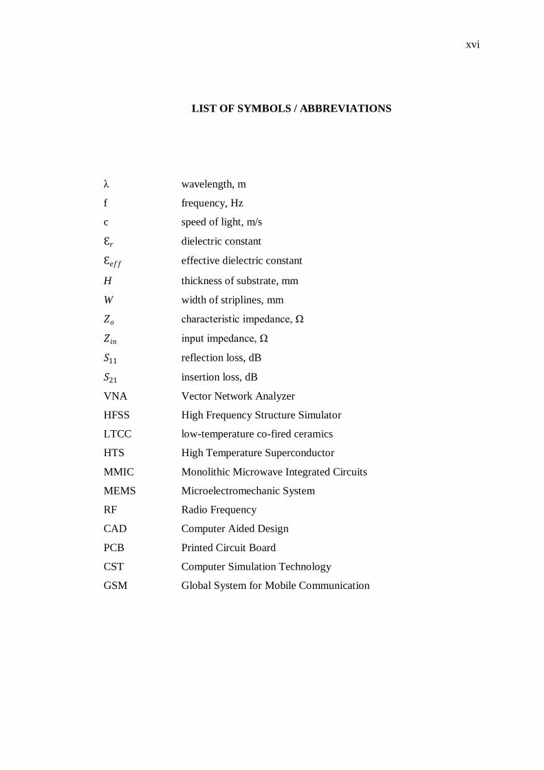
LIST OF SYMBOLS / ABBREVIATIONS
λ wavelength, m
f frequency, Hz
c speed of light, m/s
Ɛ𝑟 dielectric constant
Ɛ𝑒𝑓𝑓 effective dielectric constant
H thickness of substrate, mm
W width of striplines, mm
𝑍𝑜 characteristic impedance, Ω
𝑍𝑖𝑛 input impedance, Ω
𝑆11 reflection loss, dB
𝑆21 insertion loss, dB
VNA Vector Network Analyzer
HFSS High Frequency Structure Simulator
LTCC low-temperature co-fired ceramics
HTS High Temperature Superconductor
MMIC Monolithic Microwave Integrated Circuits
MEMS Microelectromechanic System
RF Radio Frequency
CAD Computer Aided Design
PCB Printed Circuit Board
CST Computer Simulation Technology
GSM Global System for Mobile Communication
1
CHAPTER 1
1 INTRODUCTION
1.1 Background
Bandpass filter is an electronic device that passes frequencies within a certain
range and rejects frequencies outside that range. Bandpass filters can be classified
into 2 categories: active and passive filters. An active bandpass filter requires an
external power source, and it employs active components such as transistors and
integrated circuits. It uses no external power source and consists only of passive
components such as capacitors and inductors. Such configurations are referred to as
passive filters.
Bandpass filters are used primarily in wireless transmitters and receivers. In
transmitters, the main function of such filters is to limit the bandwidth of output
signals so that power utilization can be more efficient. For a receiver, bandpass filters
remove noise from the received signal and allow only signals within certain ranges of
frequencies to pass through. Therefore, the use of bandpass filters can improve the
signal-to-noise ratio significantly.
In applications for both the transmitter and receiver, the optimized filters
must be operating in one or more than one passbands so that it can maximize the
number of channels transferring in a system, while minimizing the interference or
competition among signals.
A microstrip filter is different from those ordinary filters operating at low
frequencies, where capacitors and inductors are broadly used. Microstrip filter is
2
usually fabricated on a substrate and it does not use any electronic components. The
advantages of microstrip filter are small size, low cost, easy to fabricate, high
performance, and multi-frequency nature. According to IEEE Xplore, there have
been more than 600 publications related to microstrip filters in recent 10 years.
1.2 Research Aims and Objectives
The objective of this project is to design a microstrip dual-mode bandpass
filter that function as a balun at the same time using Ansoft High Frequency
Structure Simulator (HFSS). HFSS is a 3D Full-wave Electromagnetic Field
Simulation software. The fundamental knowledge in microstrip filter is vital in order
to design a filter with a unique configuration. Therefore, research had been done base
on the microstrip filter journals and articles that are available in IEEE Xplore
database under the UTAR OPAC system. After acquiring information and ideas from
the literature survey, a new design was implemented on designing the filter.
The aim of this project is to design a microstrip dual-mode balun filter with
good performance, ease of fabrication and simplicity. The filter is designed so that it
will have a dual-mode characteristic and the resonant frequency range must be in
between 1 to 6 GHz. There is no limitation on the size and shape of the patch and the
type of substrate used. However, size of the filter is vital in communication system as
devices are getting smaller so miniature size is also one of the aim of the design. In
addition, the filter design consists of 3 ports with 1 input and 2 outputs. The aim is to
design a filter where the input of the microwave signal is equally divided into two so
that it is also a good balun filter.
On completion of this project, students will attain knowledge on how to carry
out research, working principles of microstrip patch filter and criteria on designing a
filter with good performance. Besides that, they are able to design any microwave
devices such as antenna or filter by using High Frequency Structure Simulator
(HFSS). Students are exposed to fabrication process, experimental process and high
frequency measurement equipment in this project. Experiments are done by using
3
Vector Network Analyzer to measure the experimental results to verify with the
simulated results. Analysis of the results can be used to further improve the filter
design.
1.3 Project Motivation
The motivation of the project is to design a microstrip patch balun bandpass
filter that has good performance and publishable in an international journal. After
some literature surveys, most of the rectangular patch filters are publishable and
easier to design compare with other patch shapes. Some of the filters that had been
proposed are larger in size where size of the filter is taken into consideration in small
devices. Hence, the motivation of the project is to use a rectangular patch to design a
filter and a balun at the same time. Moreover, the motivation is to design a compact
size microstrip patch filter that able to produce a comparable result to the journal that
had been published. In addition, the novelty of the filter is it is able to divide the
microwave signal equally into two with 1800 out of phase.
4
CHAPTER 2
2 LITERATURE REVIEW
2.1 About Microstrip Filter
Microwave filters are playing important roles in various fields and industries
such as Radio Frequency (RF), wireless communication and microwave applications.
The development of microstrip filters has been in great demand due to the rapid
growth of wireless communication systems in this decade. The main purpose of filter
is to pass and reject desired band of frequencies. With the advancement of
microwave field and its achievement, it has imposed rigorous standards of
performance requirement on RF and microwave filters. Moreover, with recent
development in wireless communication, microstrip filters have been widely used in
various applications of satellite, microwave circuits, radar systems and mobile
communication systems due to its compact size and low loss characteristic. The
features such as small size, low mass, low loss, ease of fabrication, high performance
and multi-frequencies properties of microstrip filter are highly demand by the market.
In addition, the recent advance in novel materials and fabrications technologies such
as low-temperature co-fired ceramics (LTCC), high-temperature superconductor
(HTS), monolithic microwave integrated circuits (MMIC), microelectromechanic
system (MEMS) and micromachining technology had increased the development of
the new microstrip filter to a higher level.
The invention of computer-aided design (CAD) tool such as Computer
Simulation Technology (CST) and High Frequency Structure Simulator (HFSS)
makes the work of designing RF and microwave design simple. Hence, designing
5
microstrip filter is easier and it has reduced the cost of research on microstrip filter.
The reasons are that designers are able to obtain the results and observation can be
done on the simulated results without any fabrication. The development in
microwave designing tools and increase of computer processing power had
contributed to the growth of microwave research area. A powerful CAD tool is able
to produce simulation results that are comparable to experimental results which give
a high degree of accuracy. Ansoft High Frequency Structure Simulator (HFSS) has
been used in this project as CAD tools for the microstrip filter design.
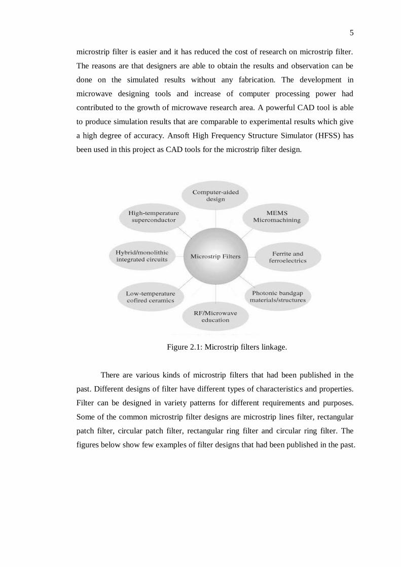
Figure 2.1: Microstrip filters linkage.
There are various kinds of microstrip filters that had been published in the
past. Different designs of filter have different types of characteristics and properties.
Filter can be designed in variety patterns for different requirements and purposes.
Some of the common microstrip filter designs are microstrip lines filter, rectangular
patch filter, circular patch filter, rectangular ring filter and circular ring filter. The
figures below show few examples of filter designs that had been published in the past.
6
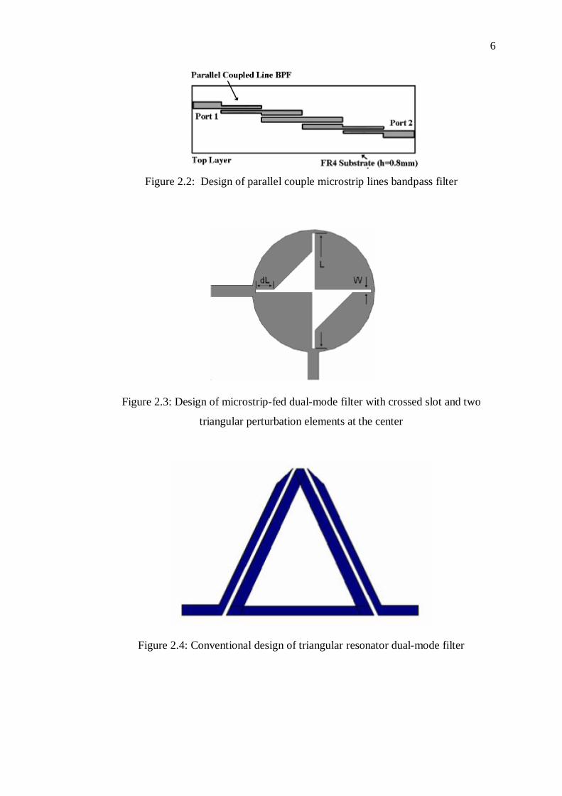
Figure 2.2: Design of parallel couple microstrip lines bandpass filter
Figure 2.3: Design of microstrip-fed dual-mode filter with crossed slot and two
triangular perturbation elements at the center
Figure 2.4: Conventional design of triangular resonator dual-mode filter
7
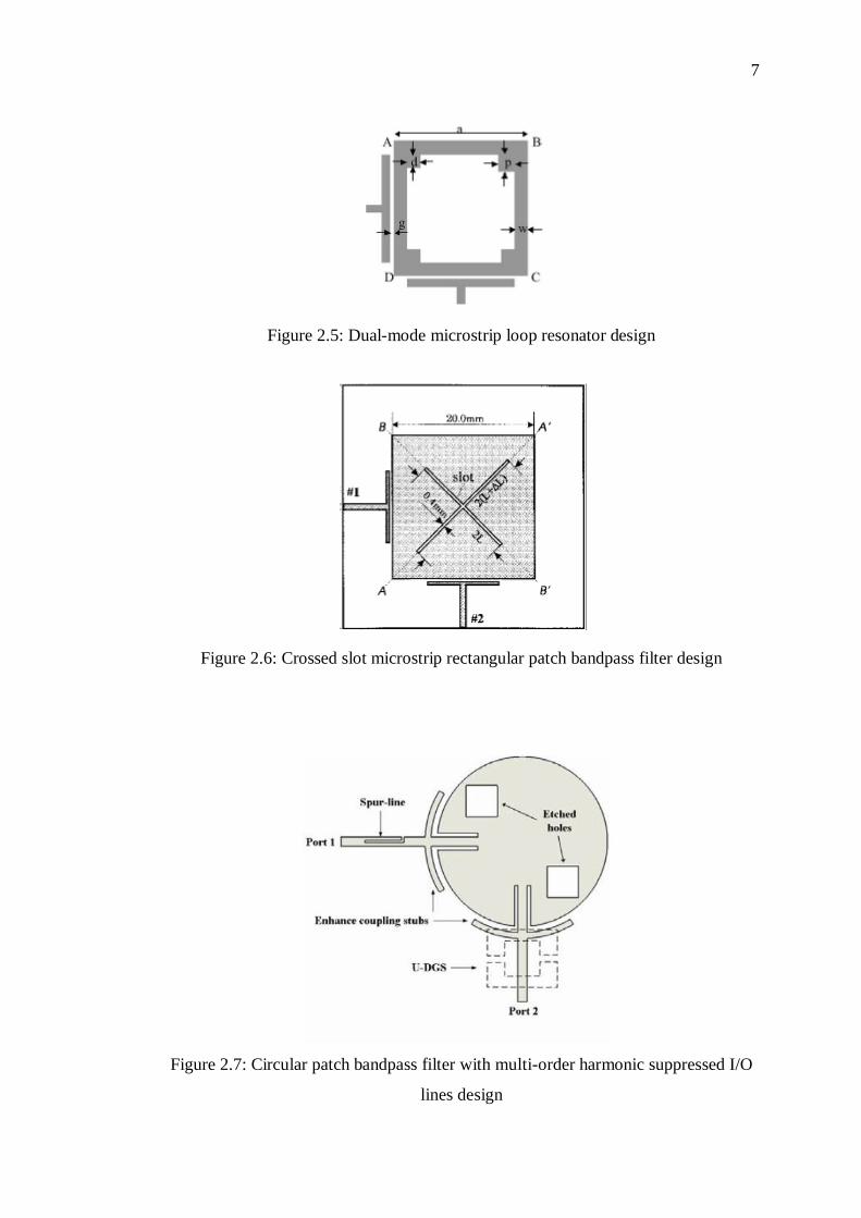
Figure 2.5: Dual-mode microstrip loop resonator design
Figure 2.6: Crossed slot microstrip rectangular patch bandpass filter design
Figure 2.7: Circular patch bandpass filter with multi-order harmonic suppressed I/O
lines design
8
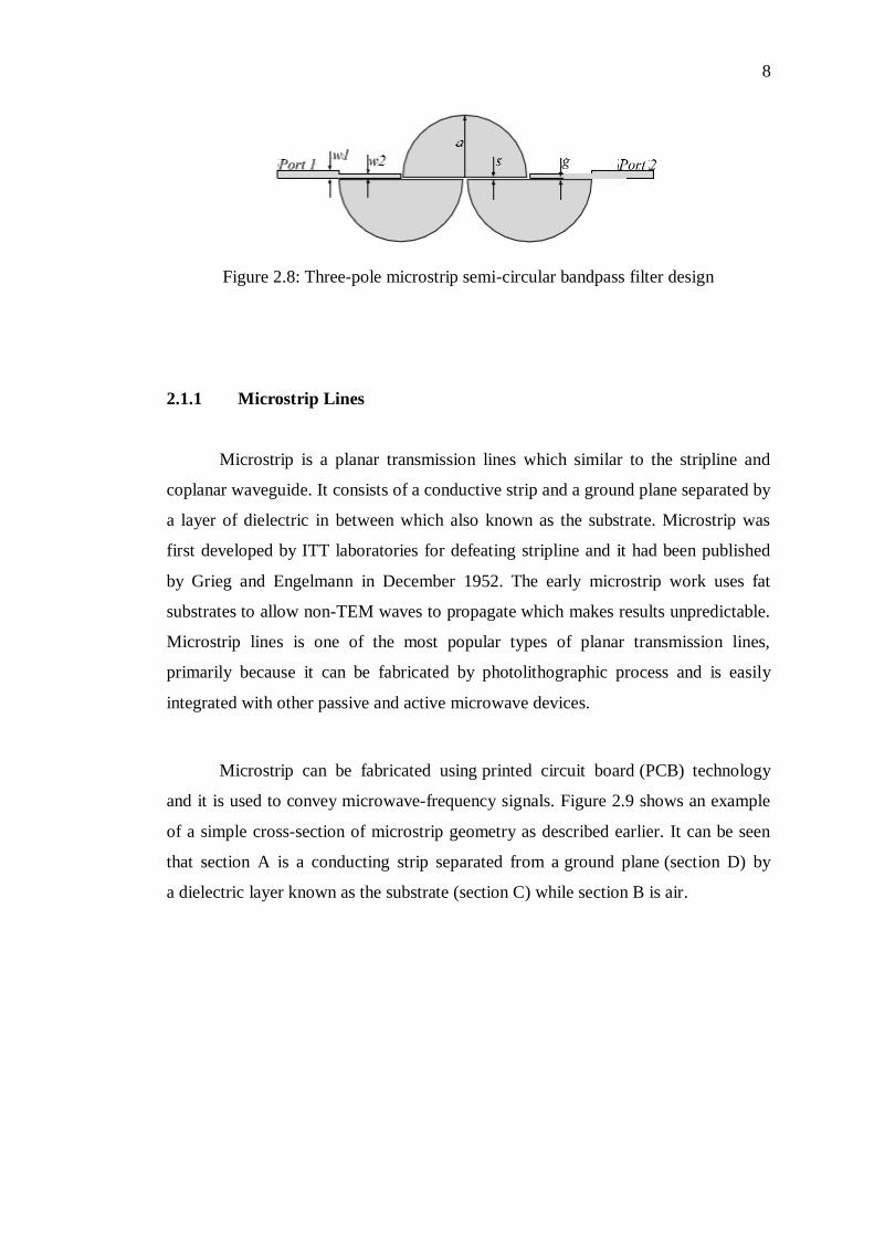
Figure 2.8: Three-pole microstrip semi-circular bandpass filter design
2.1.1 Microstrip Lines
Microstrip is a planar transmission lines which similar to the stripline and
coplanar waveguide. It consists of a conductive strip and a ground plane separated by
a layer of dielectric in between which also known as the substrate. Microstrip was
first developed by ITT laboratories for defeating stripline and it had been published
by Grieg and Engelmann in December 1952. The early microstrip work uses fat
substrates to allow non-TEM waves to propagate which makes results unpredictable.
Microstrip lines is one of the most popular types of planar transmission lines,
primarily because it can be fabricated by photolithographic process and is easily
integrated with other passive and active microwave devices.
Microstrip can be fabricated using printed circuit board (PCB) technology
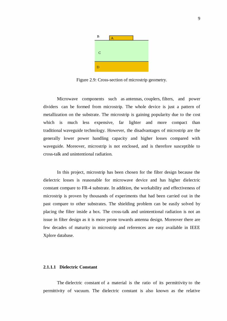
and it is used to convey microwave-frequency signals. Figure 2.9 shows an example
of a simple cross-section of microstrip geometry as described earlier. It can be seen
that section A is a conducting strip separated from a ground plane (section D) by
a dielectric layer known as the substrate (section C) while section B is air.
9
Figure 2.9: Cross-section of microstrip geometry.
Microwave components such as antennas, couplers, filters, and power
dividers can be formed from microstrip. The whole device is just a pattern of
metallization on the substrate. The microstrip is gaining popularity due to the cost
which is much less expensive, far lighter and more compact than
traditional waveguide technology. However, the disadvantages of microstrip are the
generally lower power handling capacity and higher losses compared with
waveguide. Moreover, microstrip is not enclosed, and is therefore susceptible to
cross-talk and unintentional radiation.
In this project, microstrip has been chosen for the filter design because the
dielectric losses is reasonable for microwave device and has higher dielectric
constant compare to FR-4 substrate. In addition, the workability and effectiveness of
microstrip is proven by thousands of experiments that had been carried out in the
past compare to other substrates. The shielding problem can be easily solved by
placing the filter inside a box. The cross-talk and unintentional radiation is not an
issue in filter design as it is more prone towards antenna design. Moreover there are
few decades of maturity in microstrip and references are easy available in IEEE
Xplore database.
2.1.1.1 Dielectric Constant
The dielectric constant of a material is the ratio of its permittivity to the
permittivity of vacuum. The dielectric constant is also known as the relative
10
permittivity of the material. Hence, it is a measure of the extent to which it
concentrates electrostatic lines of flux. Different substrates are made from different
materials which have different dielectric constants. Microstrip can be fabricated on
different substrates based on the requirement of the design. Some designs do not
require high dielectric constant and therefore FR-4 substrate which has dielectric
constant of 4.4 can be use. FR-4 substrate is much cheaper as compared to
RT/Duroid 6006 which has dielectric constant of 6.15. Dielectric constant is
frequency dependent. For instance, the dielectric of FR-4 is 4.35 at 500MHz and 4.34
at 1GHz. There is a 0.01 difference in the dielectric constant in 500MHz variation,
which is around 0.23% variation per 500MHz.
In this project, RT/Duroid 6006 has been chosen as the substrate for the
microstrip filter design because it require higher dielectric constant which having
lower losses. In addition, the filter design in this project is in the range of high
frequency where FR-4 will not be suitable to use as a substrate. Although RT/Duroid
6006 is more expensive, the cost will not put on priority due to the filter design
requirement. The substrate is expensive because it is relatively thin and high in
dielectric constant. RT/Duroid 6006 substrate is not available in the Malaysia and has
to order from Rogers Corporation in United State. The substrate came with a
dimension of 25.4cm x 25.4cm.
2.1.1.2 Effective Dielectric Constant
Effective dielectric constant can be interpreted as the dielectric constant of a
homogeneous medium that replaces the air and the dielectric regions of the
microstrip. In general, the dielectric constant of a substrate will be greater than air.
Hence the electromagnetic wave is travelling in an inhomogeneous medium and
propagation velocity is affected by the dielectric constant. The propagation velocity
falls between the speed of radio waves in the substrate and the speed of radio waves
in air. Normally, the effective dielectric constant is slightly less than the substrate
dielectric constant because part of the fields from the microstrip conductor exists in
the air.
11
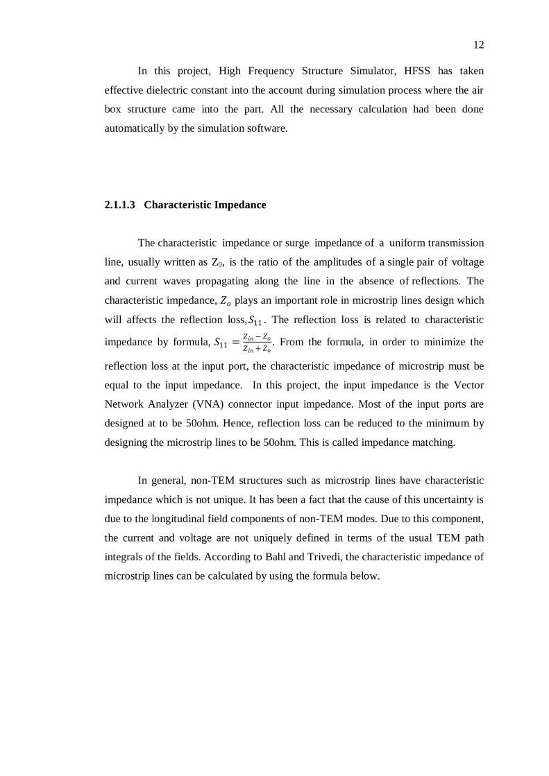
According to Bahl and Trivedi, the effective dielectric constant can be
calculated by using the formula below where W represents the width of the
microstripline, H is the height of the substrate and Ɛr represents dielectric constant of
the substrate. There are separate solutions for cases where W/H is less than 1 and
when W/H is greater than or equal to 1. The formula used is just a reasonable
approximation for the effective dielectric constant because it ignored microstrip lines
thickness and frequency dispersion. However their effects are usually small and
reasonably acceptable.
Figure 2.10 : Substrate
The inhomogeneous medium will cause the line to not support a true TEM
wave at non-zero frequencies, and both E field and H field will have longitudinal
components. However, the longitudinal components are small and the dominant
mode is referred to as quasi-TEM. Meanwhile, the microstrip lines are dispersive in
inhomogeneous medium. The effective dielectric constant will gradually increase
towards the substrate with the increasing frequency so that the phase velocity will
slowly decrease.
H
W
12
In this project, High Frequency Structure Simulator, HFSS has taken
effective dielectric constant into the account during simulation process where the air
box structure came into the part. All the necessary calculation had been done
automatically by the simulation software.
2.1.1.3 Characteristic Impedance
The characteristic impedance or surge impedance of a uniform transmission
line, usually written as Z0, is the ratio of the amplitudes of a single pair of voltage
and current waves propagating along the line in the absence of reflections. The
characteristic impedance, 𝑍𝑜 plays an important role in microstrip lines design which
will affects the reflection loss,𝑆11 . The reflection loss is related to characteristic
impedance by formula, 𝑆11 =𝑍𝑖𝑛− 𝑍𝑜
𝑍𝑖𝑛 + 𝑍𝑜. From the formula, in order to minimize the
reflection loss at the input port, the characteristic impedance of microstrip must be
equal to the input impedance. In this project, the input impedance is the Vector
Network Analyzer (VNA) connector input impedance. Most of the input ports are
designed at to be 50ohm. Hence, reflection loss can be reduced to the minimum by
designing the microstrip lines to be 50ohm. This is called impedance matching.
In general, non-TEM structures such as microstrip lines have characteristic
impedance which is not unique. It has been a fact that the cause of this uncertainty is
due to the longitudinal field components of non-TEM modes. Due to this component,
the current and voltage are not uniquely defined in terms of the usual TEM path
integrals of the fields. According to Bahl and Trivedi, the characteristic impedance of
microstrip lines can be calculated by using the formula below.
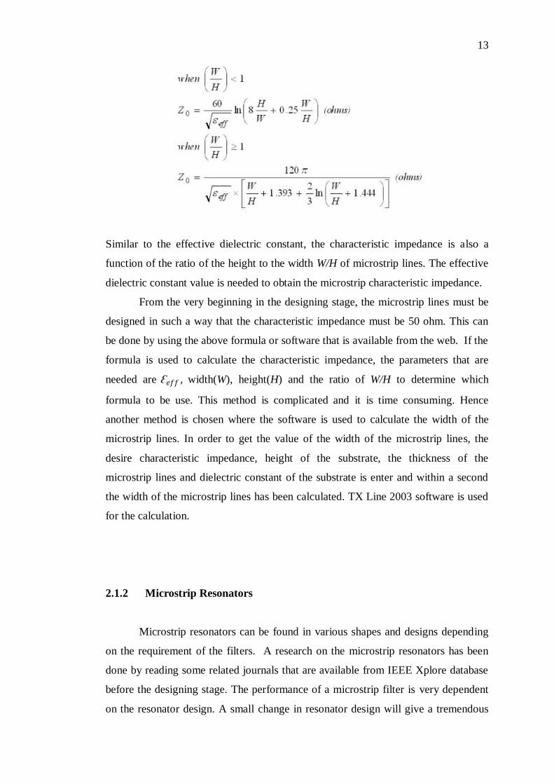
13
Similar to the effective dielectric constant, the characteristic impedance is also a
function of the ratio of the height to the width W/H of microstrip lines. The effective
dielectric constant value is needed to obtain the microstrip characteristic impedance.
From the very beginning in the designing stage, the microstrip lines must be
designed in such a way that the characteristic impedance must be 50 ohm. This can
be done by using the above formula or software that is available from the web. If the
formula is used to calculate the characteristic impedance, the parameters that are
needed are Ɛ𝑒𝑓𝑓 , width(W), height(H) and the ratio of W/H to determine which
formula to be use. This method is complicated and it is time consuming. Hence
another method is chosen where the software is used to calculate the width of the
microstrip lines. In order to get the value of the width of the microstrip lines, the
desire characteristic impedance, height of the substrate, the thickness of the
microstrip lines and dielectric constant of the substrate is enter and within a second
the width of the microstrip lines has been calculated. TX Line 2003 software is used
for the calculation.
2.1.2 Microstrip Resonators
Microstrip resonators can be found in various shapes and designs depending
on the requirement of the filters. A research on the microstrip resonators has been
done by reading some related journals that are available from IEEE Xplore database
before the designing stage. The performance of a microstrip filter is very dependent
on the resonator design. A small change in resonator design will give a tremendous
14
effect on the results. The author has chosen a few types of resonators that will be
discussed in more detail in next sub-chapter. The types of resonators that will be
discussed are cross-slotted patch resonator, circular patch resonator and triangular
loop resonator.
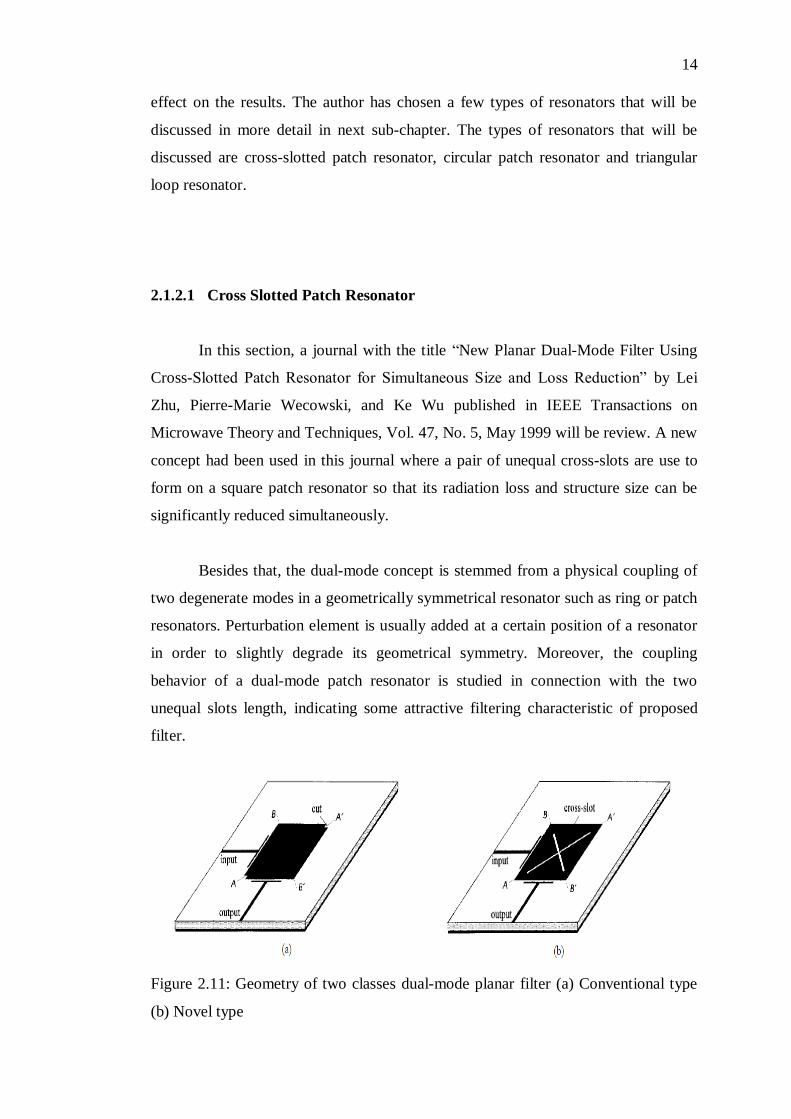
2.1.2.1 Cross Slotted Patch Resonator
In this section, a journal with the title “New Planar Dual-Mode Filter Using
Cross-Slotted Patch Resonator for Simultaneous Size and Loss Reduction” by Lei
Zhu, Pierre-Marie Wecowski, and Ke Wu published in IEEE Transactions on
Microwave Theory and Techniques, Vol. 47, No. 5, May 1999 will be review. A new
concept had been used in this journal where a pair of unequal cross-slots are use to
form on a square patch resonator so that its radiation loss and structure size can be
significantly reduced simultaneously.
Besides that, the dual-mode concept is stemmed from a physical coupling of
two degenerate modes in a geometrically symmetrical resonator such as ring or patch
resonators. Perturbation element is usually added at a certain position of a resonator
in order to slightly degrade its geometrical symmetry. Moreover, the coupling
behavior of a dual-mode patch resonator is studied in connection with the two
unequal slots length, indicating some attractive filtering characteristic of proposed
filter.
Figure 2.11: Geometry of two classes dual-mode planar filter (a) Conventional type
(b) Novel type
15
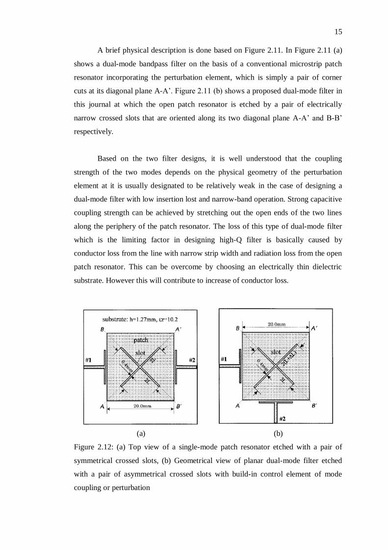
A brief physical description is done based on Figure 2.11. In Figure 2.11 (a)
shows a dual-mode bandpass filter on the basis of a conventional microstrip patch
resonator incorporating the perturbation element, which is simply a pair of corner
cuts at its diagonal plane A-A‟. Figure 2.11 (b) shows a proposed dual-mode filter in
this journal at which the open patch resonator is etched by a pair of electrically
narrow crossed slots that are oriented along its two diagonal plane A-A‟ and B-B‟
respectively.
Based on the two filter designs, it is well understood that the coupling
strength of the two modes depends on the physical geometry of the perturbation
element at it is usually designated to be relatively weak in the case of designing a
dual-mode filter with low insertion lost and narrow-band operation. Strong capacitive
coupling strength can be achieved by stretching out the open ends of the two lines
along the periphery of the patch resonator. The loss of this type of dual-mode filter
which is the limiting factor in designing high-Q filter is basically caused by
conductor loss from the line with narrow strip width and radiation loss from the open
patch resonator. This can be overcome by choosing an electrically thin dielectric
substrate. However this will contribute to increase of conductor loss.
(a) (b)
Figure 2.12: (a) Top view of a single-mode patch resonator etched with a pair of
symmetrical crossed slots, (b) Geometrical view of planar dual-mode filter etched
with a pair of asymmetrical crossed slots with build-in control element of mode
coupling or perturbation
16
The features of a single mode resonator circuit are applied to the design of a
low loss dual-mode filter by rearranging the orientation of the two externally
connected lines and also by adequately differentiating the two slots length to produce
the coupling between the two degenerate modes. The perturbation element
introduced is similar to the corner cut which is responsible for the coupling between
the degenerate modes in the patch resonator.
(a) (b)
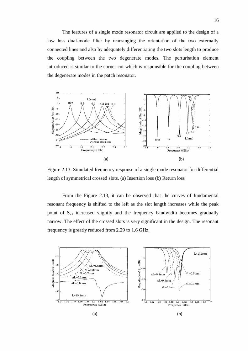
Figure 2.13: Simulated frequency response of a single mode resonator for differential
length of symmetrical crossed slots, (a) Insertion loss (b) Return loss
From the Figure 2.13, it can be observed that the curves of fundamental
resonant frequency is shifted to the left as the slot length increases while the peak
point of S21 increased slightly and the frequency bandwidth becomes gradually
narrow. The effect of the crossed slots is very significant in the design. The resonant
frequency is greatly reduced from 2.29 to 1.6 GHz.
(a) (b)
17
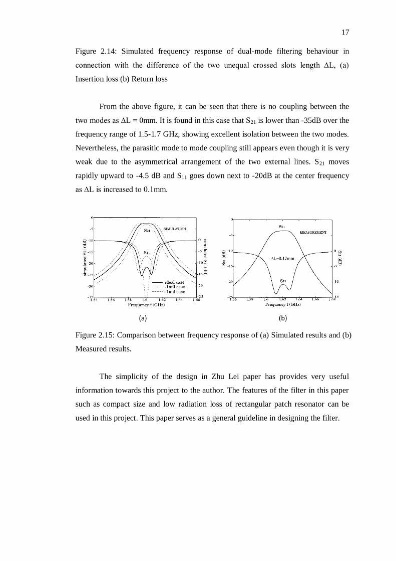
Figure 2.14: Simulated frequency response of dual-mode filtering behaviour in
connection with the difference of the two unequal crossed slots length ∆L, (a)
Insertion loss (b) Return loss
From the above figure, it can be seen that there is no coupling between the
two modes as ∆L = 0mm. It is found in this case that S21 is lower than -35dB over the
frequency range of 1.5-1.7 GHz, showing excellent isolation between the two modes.
Nevertheless, the parasitic mode to mode coupling still appears even though it is very
weak due to the asymmetrical arrangement of the two external lines. S21 moves
rapidly upward to -4.5 dB and S11 goes down next to -20dB at the center frequency
as ∆L is increased to 0.1mm.
(a) (b)
Figure 2.15: Comparison between frequency response of (a) Simulated results and (b)
Measured results.
The simplicity of the design in Zhu Lei paper has provides very useful
information towards this project to the author. The features of the filter in this paper
such as compact size and low radiation loss of rectangular patch resonator can be
used in this project. This paper serves as a general guideline in designing the filter.
18
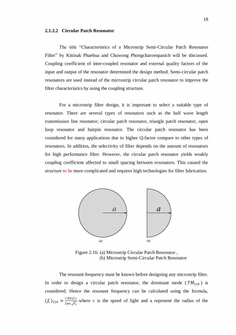
2.1.2.2 Circular Patch Resonator
The title “Characteristics of a Microstrip Semi-Circular Patch Resonator
Filter” by Kittisak Phaebua and Chuwong Phongcharoenpanich will be discussed.
Coupling coefficient of inter-coupled resonator and external quality factors of the
input and output of the resonator determined the design method. Semi-circular patch
resonators are used instead of the microstrip circular patch resonator to improve the
filter characteristics by using the coupling structure.
For a microstrip filter design, it is important to select a suitable type of
resonator. There are several types of resonators such as the half wave length
transmission line resonator, circular patch resonator, triangle patch resonator, open
loop resonator and hairpin resonator. The circular patch resonator has been
considered for many applications due to higher Q-factor compare to other types of
resonators. In addition, the selectivity of filter depends on the amount of resonators
for high performance filter. However, the circular patch resonator yields weakly
coupling coefficient affected to small spacing between resonators. This caused the
structure to be more complicated and requires high technologies for filter fabrication.
Figure 2.16: (a) Microstrip Circular Patch Resonator ,
(b) Microstrip Semi-Circular Patch Resonator
The resonant frequency must be known before designing any microstrip filter.
In order to design a circular patch resonator, the dominant mode ( 𝑇𝑀110 ) is
considered. Hence the resonant frequency can be calculated using the formula,
(𝑓𝑟)110 =1.8412𝑐
2𝜋𝑎 Ɛ𝑟 where c is the speed of light and a represent the radius of the
19
circular patch. The substrate used in designing this filter is Roger RT 3003 with
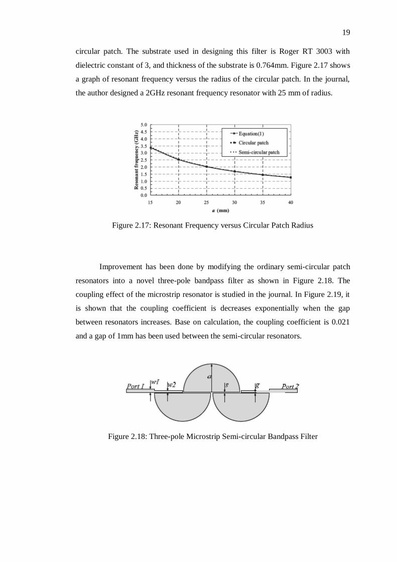
dielectric constant of 3, and thickness of the substrate is 0.764mm. Figure 2.17 shows
a graph of resonant frequency versus the radius of the circular patch. In the journal,
the author designed a 2GHz resonant frequency resonator with 25 mm of radius.
Figure 2.17: Resonant Frequency versus Circular Patch Radius
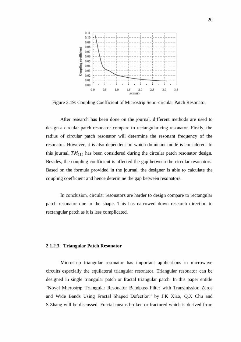
Improvement has been done by modifying the ordinary semi-circular patch
resonators into a novel three-pole bandpass filter as shown in Figure 2.18. The
coupling effect of the microstrip resonator is studied in the journal. In Figure 2.19, it
is shown that the coupling coefficient is decreases exponentially when the gap
between resonators increases. Base on calculation, the coupling coefficient is 0.021
and a gap of 1mm has been used between the semi-circular resonators.
Figure 2.18: Three-pole Microstrip Semi-circular Bandpass Filter
20
Figure 2.19: Coupling Coefficient of Microstrip Semi-circular Patch Resonator
After research has been done on the journal, different methods are used to
design a circular patch resonator compare to rectangular ring resonator. Firstly, the
radius of circular patch resonator will determine the resonant frequency of the
resonator. However, it is also dependent on which dominant mode is considered. In
this journal, 𝑇𝑀110 has been considered during the circular patch resonator design.
Besides, the coupling coefficient is affected the gap between the circular resonators.
Based on the formula provided in the journal, the designer is able to calculate the
coupling coefficient and hence determine the gap between resonators.
In conclusion, circular resonators are harder to design compare to rectangular
patch resonator due to the shape. This has narrowed down research direction to
rectangular patch as it is less complicated.
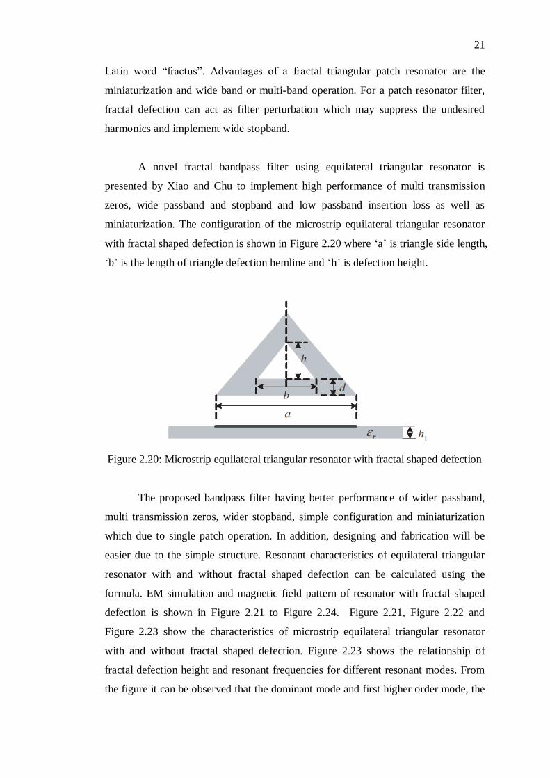
2.1.2.3 Triangular Patch Resonator
Microstrip triangular resonator has important applications in microwave
circuits especially the equilateral triangular resonator. Triangular resonator can be
designed in single triangular patch or fractal triangular patch. In this paper entitle
“Novel Microstrip Triangular Resonator Bandpass Filter with Transmission Zeros
and Wide Bands Using Fractal Shaped Defection” by J.K Xiao, Q.X Chu and
S.Zhang will be discussed. Fractal means broken or fractured which is derived from
21
Latin word “fractus”. Advantages of a fractal triangular patch resonator are the
miniaturization and wide band or multi-band operation. For a patch resonator filter,
fractal defection can act as filter perturbation which may suppress the undesired
harmonics and implement wide stopband.
A novel fractal bandpass filter using equilateral triangular resonator is
presented by Xiao and Chu to implement high performance of multi transmission
zeros, wide passband and stopband and low passband insertion loss as well as
miniaturization. The configuration of the microstrip equilateral triangular resonator
with fractal shaped defection is shown in Figure 2.20 where „a‟ is triangle side length,
„b‟ is the length of triangle defection hemline and „h‟ is defection height.
Figure 2.20: Microstrip equilateral triangular resonator with fractal shaped defection
The proposed bandpass filter having better performance of wider passband,
multi transmission zeros, wider stopband, simple configuration and miniaturization
which due to single patch operation. In addition, designing and fabrication will be
easier due to the simple structure. Resonant characteristics of equilateral triangular
resonator with and without fractal shaped defection can be calculated using the
formula. EM simulation and magnetic field pattern of resonator with fractal shaped
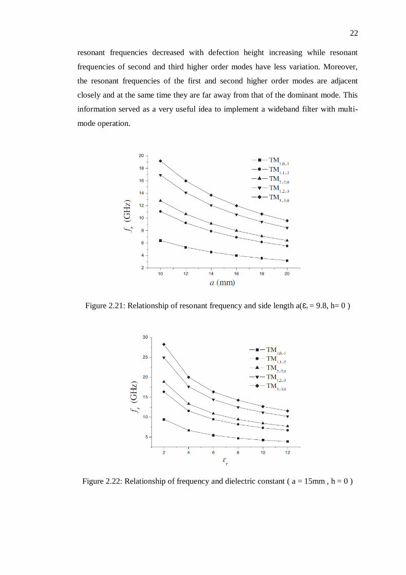
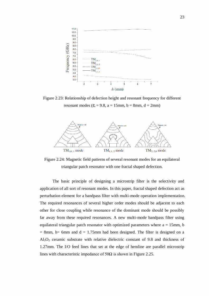
defection is shown in Figure 2.21 to Figure 2.24. Figure 2.21, Figure 2.22 and
Figure 2.23 show the characteristics of microstrip equilateral triangular resonator
with and without fractal shaped defection. Figure 2.23 shows the relationship of
fractal defection height and resonant frequencies for different resonant modes. From
the figure it can be observed that the dominant mode and first higher order mode, the
22
resonant frequencies decreased with defection height increasing while resonant
frequencies of second and third higher order modes have less variation. Moreover,
the resonant frequencies of the first and second higher order modes are adjacent
closely and at the same time they are far away from that of the dominant mode. This
information served as a very useful idea to implement a wideband filter with multi-
mode operation.
Figure 2.21: Relationship of resonant frequency and side length a(Ɛr = 9.8, h= 0 )
Figure 2.22: Relationship of frequency and dielectric constant ( a = 15mm , h = 0 )
23
Figure 2.23: Relationship of defection height and resonant frequency for different
resonant modes (Ɛr = 9.8, a = 15mm, b = 8mm, d = 2mm)
Figure 2.24: Magnetic field patterns of several resonant modes for an equilateral
triangular patch resonator with one fractal shaped defection.
The basic principle of designing a microstrip filter is the selectivity and
application of all sort of resonant modes. In this paper, fractal shaped defection act as
perturbation element for a bandpass filter with multi-mode operation implementation.
The required resonances of several higher order modes should be adjacent to each
other for close coupling while resonance of the dominant mode should be possibly
far away from these required resonances. A new multi-mode bandpass filter using
equilateral triangular patch resonator with optimized parameters where a = 15mm, b
= 8mm, h= 6mm and d = 1.75mm had been designed. The filter is designed on a
Al3O2 ceramic substrate with relative dielectric constant of 9.8 and thickness of
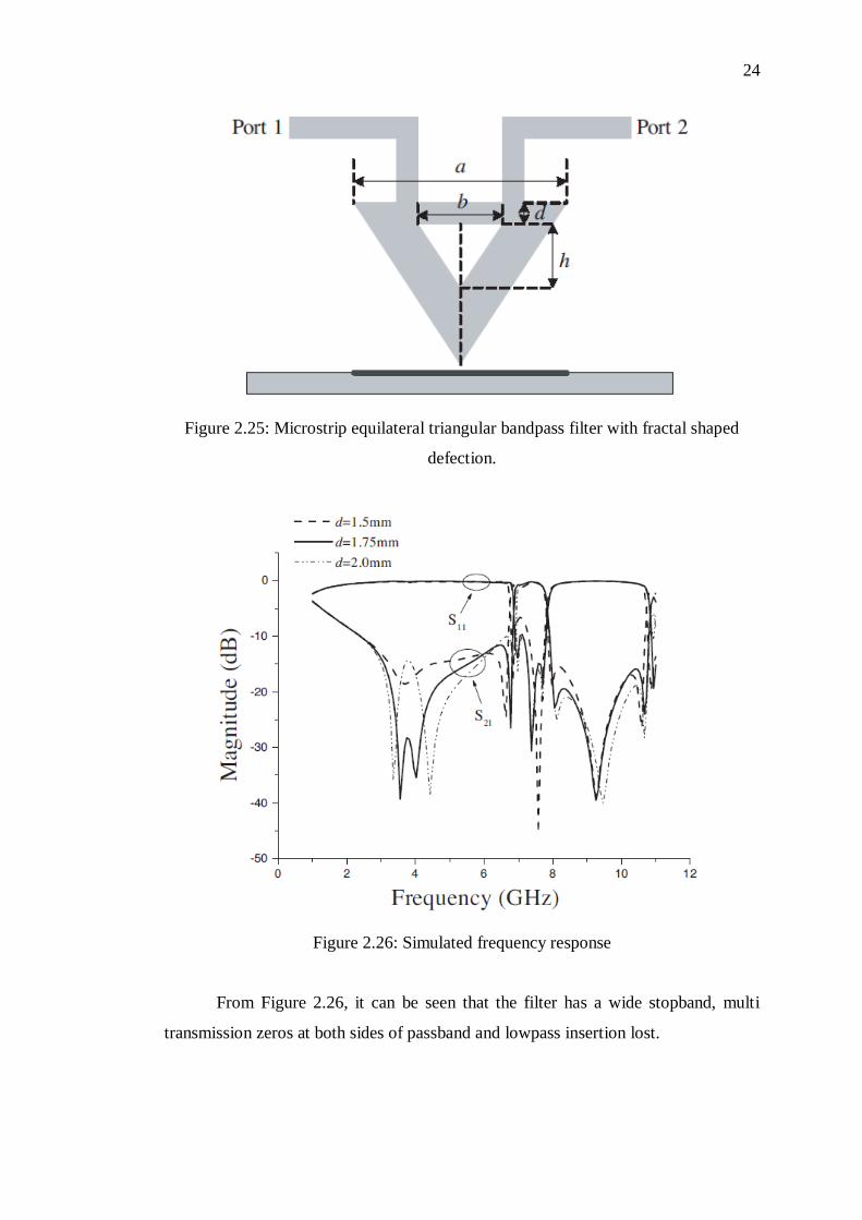
1.27mm. The I/O feed lines that set at the edge of hemline are parallel microstrip
lines with characteristic impedance of 50Ω is shown in Figure 2.25.
24
Figure 2.25: Microstrip equilateral triangular bandpass filter with fractal shaped
defection.
Figure 2.26: Simulated frequency response
From Figure 2.26, it can be seen that the filter has a wide stopband, multi
transmission zeros at both sides of passband and lowpass insertion lost.
25
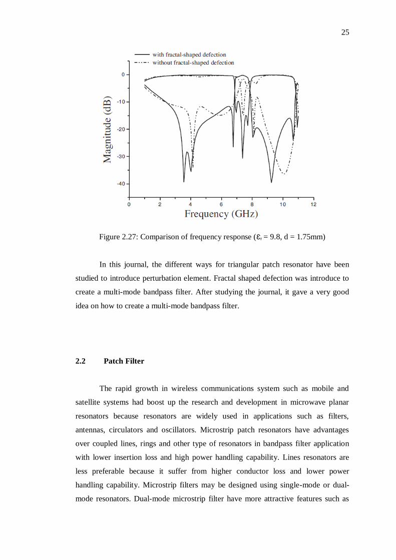
Figure 2.27: Comparison of frequency response (Ɛr = 9.8, d = 1.75mm)
In this journal, the different ways for triangular patch resonator have been
studied to introduce perturbation element. Fractal shaped defection was introduce to
create a multi-mode bandpass filter. After studying the journal, it gave a very good
idea on how to create a multi-mode bandpass filter.
2.2 Patch Filter
The rapid growth in wireless communications system such as mobile and
satellite systems had boost up the research and development in microwave planar
resonators because resonators are widely used in applications such as filters,
antennas, circulators and oscillators. Microstrip patch resonators have advantages
over coupled lines, rings and other type of resonators in bandpass filter application
with lower insertion loss and high power handling capability. Lines resonators are
less preferable because it suffer from higher conductor loss and lower power
handling capability. Microstrip filters may be designed using single-mode or dual-
mode resonators. Dual-mode microstrip filter have more attractive features such as

26
each resonator can behave as a doubly tuned resonant circuit and reducing by half the
number of resonators required for a given filter. In this chapter, single-mode and
dual-mode patch resonators will be discussed.
2.2.1 Applications of Patch Resonator
As mention before, patch resonators are more attractive compare to other
resonators in terms of low insertion loss and high power handling capability. The
only drawback of a patch resonator compared to other resonators is the size of the
resonator which is slightly larger. Although patch resonators have a larger size, this
drawback is not a big issue for the applications because the power handling or low
loss has a higher priority. Furthermore, the size may not be a problem as the filters
operate at very high frequencies. Patch resonators usually tend to have a stronger
radiation due to high power handling capability. Filters are normally enclosed in a
metal housing for filter applications so that the radiation loss can be minimized.
Depending on the filter design requirements or applications, patch resonator may be
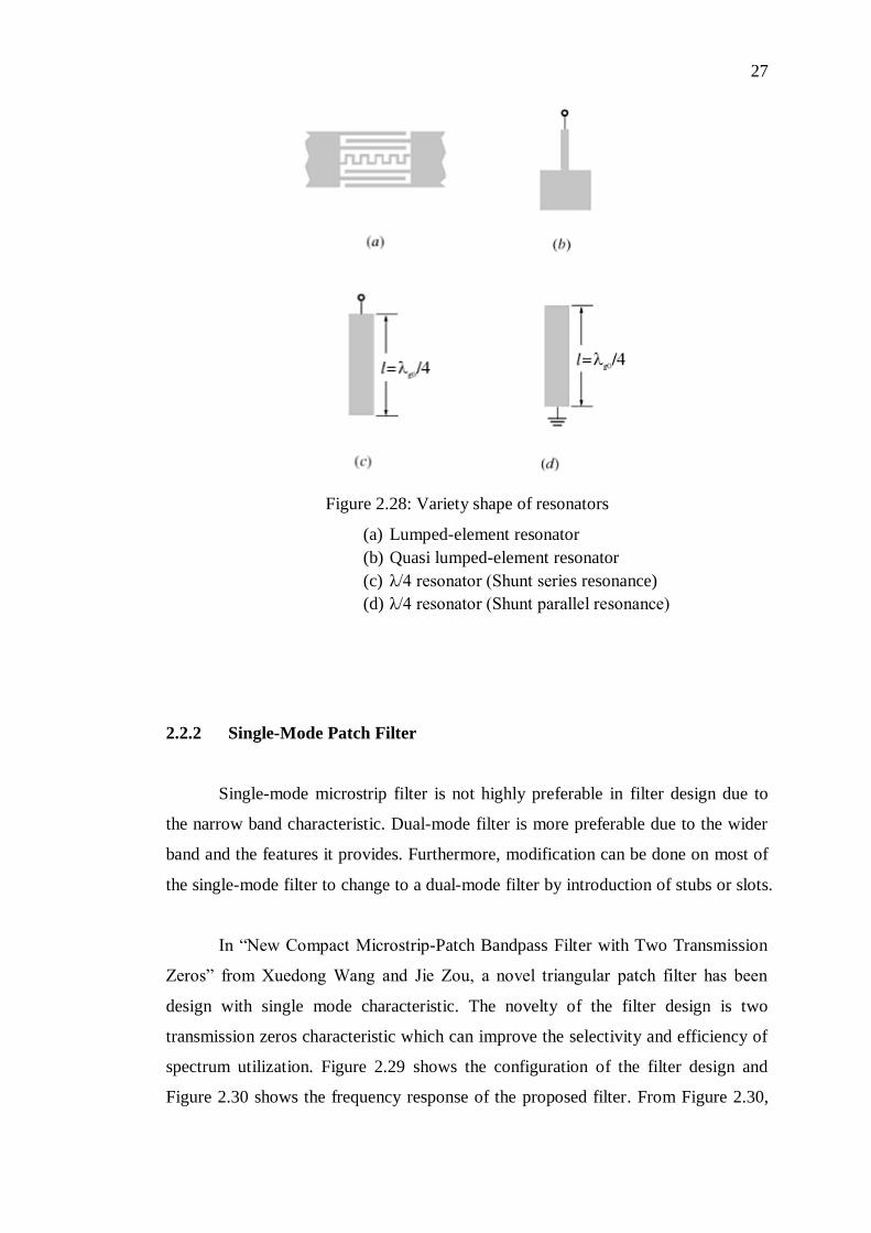
designed in different shapes as shown in Figure 2.28. Nowadays, patch resonator
filters are widely employed in wireless communication systems especially in mobile
communication systems. For instance, Global System for Mobile (GSM) mobile
phones are using dual-mode patch filter which just pass 900MHz and 1800MHz
signal.
27
Figure 2.28: Variety shape of resonators
(a) Lumped-element resonator
(b) Quasi lumped-element resonator
(c) λ/4 resonator (Shunt series resonance)
(d) λ/4 resonator (Shunt parallel resonance)
2.2.2 Single-Mode Patch Filter
Single-mode microstrip filter is not highly preferable in filter design due to
the narrow band characteristic. Dual-mode filter is more preferable due to the wider
band and the features it provides. Furthermore, modification can be done on most of
the single-mode filter to change to a dual-mode filter by introduction of stubs or slots.
In “New Compact Microstrip-Patch Bandpass Filter with Two Transmission
Zeros” from Xuedong Wang and Jie Zou, a novel triangular patch filter has been
design with single mode characteristic. The novelty of the filter design is two
transmission zeros characteristic which can improve the selectivity and efficiency of
spectrum utilization. Figure 2.29 shows the configuration of the filter design and
Figure 2.30 shows the frequency response of the proposed filter. From Figure 2.30,
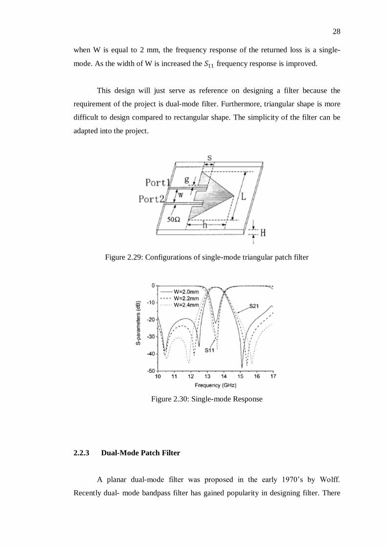
28
when W is equal to 2 mm, the frequency response of the returned loss is a single-
mode. As the width of W is increased the 𝑆11 frequency response is improved.
This design will just serve as reference on designing a filter because the
requirement of the project is dual-mode filter. Furthermore, triangular shape is more
difficult to design compared to rectangular shape. The simplicity of the filter can be
adapted into the project.
Figure 2.29: Configurations of single-mode triangular patch filter
Figure 2.30: Single-mode Response
2.2.3 Dual-Mode Patch Filter
A planar dual-mode filter was proposed in the early 1970‟s by Wolff.
Recently dual- mode bandpass filter has gained popularity in designing filter. There
29
are many dual-mode filter structures which have been proposed. However due to
high coupling loss between feed line and resonator, their application is narrow down.
In this paper with the tile “Compact and Low Insertion Loss Dual Mode Bandpass
Filter” by Y.Sung is reviewed. The proposed filter provides low insertion loss
because there is no coupling gap and radiation loss in feed structure. The impedance
matching can be easily obtained without the coupling gap between feed line and
patch resonator.
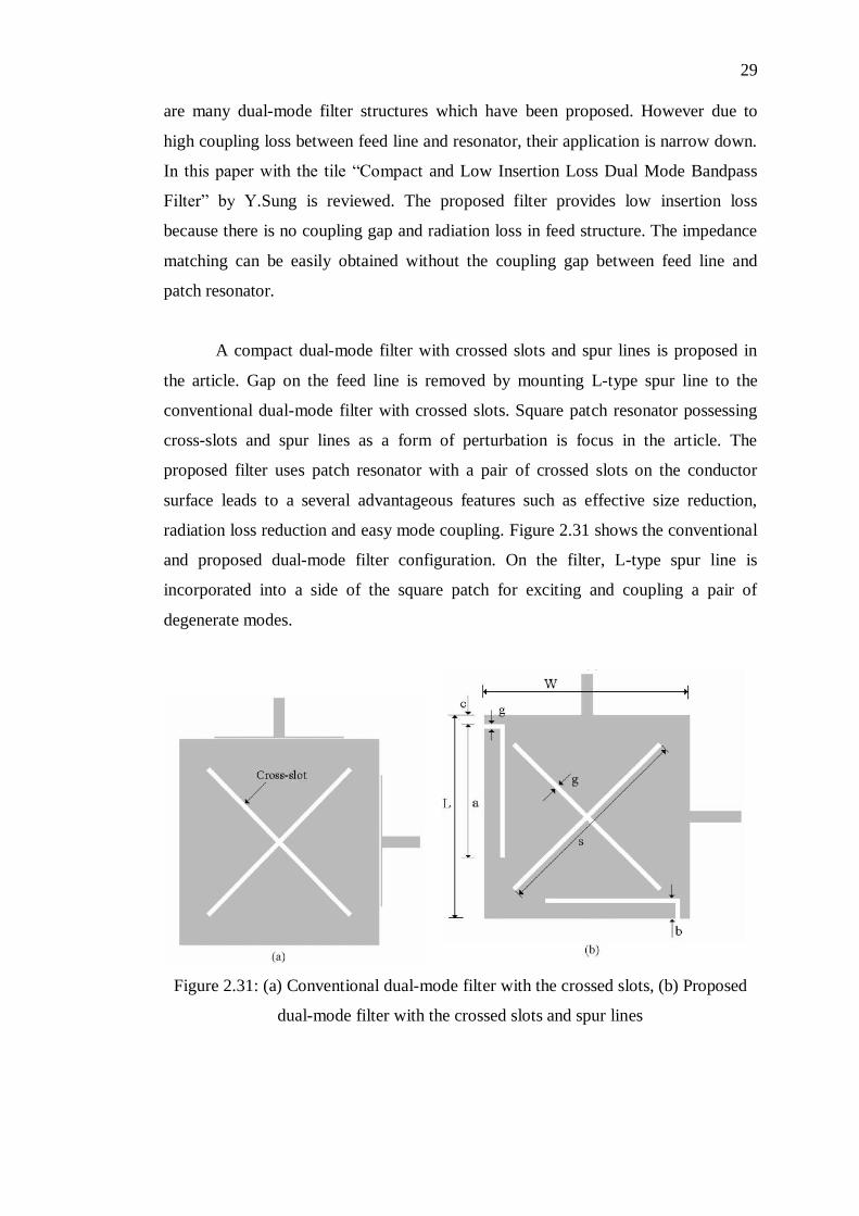
A compact dual-mode filter with crossed slots and spur lines is proposed in
the article. Gap on the feed line is removed by mounting L-type spur line to the
conventional dual-mode filter with crossed slots. Square patch resonator possessing
cross-slots and spur lines as a form of perturbation is focus in the article. The
proposed filter uses patch resonator with a pair of crossed slots on the conductor
surface leads to a several advantageous features such as effective size reduction,
radiation loss reduction and easy mode coupling. Figure 2.31 shows the conventional
and proposed dual-mode filter configuration. On the filter, L-type spur line is
incorporated into a side of the square patch for exciting and coupling a pair of
degenerate modes.
Figure 2.31: (a) Conventional dual-mode filter with the crossed slots, (b) Proposed
dual-mode filter with the crossed slots and spur lines
30
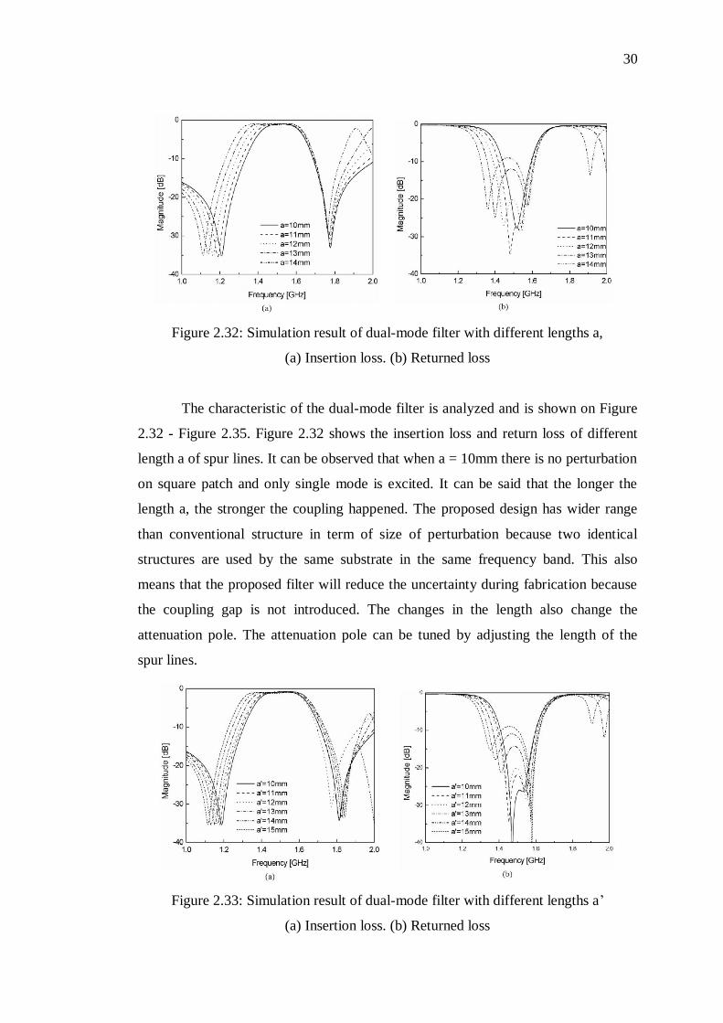
Figure 2.32: Simulation result of dual-mode filter with different lengths a,
(a) Insertion loss. (b) Returned loss
The characteristic of the dual-mode filter is analyzed and is shown on Figure
2.32 - Figure 2.35. Figure 2.32 shows the insertion loss and return loss of different
length a of spur lines. It can be observed that when a = 10mm there is no perturbation
on square patch and only single mode is excited. It can be said that the longer the
length a, the stronger the coupling happened. The proposed design has wider range
than conventional structure in term of size of perturbation because two identical
structures are used by the same substrate in the same frequency band. This also
means that the proposed filter will reduce the uncertainty during fabrication because
the coupling gap is not introduced. The changes in the length also change the
attenuation pole. The attenuation pole can be tuned by adjusting the length of the
spur lines.
Figure 2.33: Simulation result of dual-mode filter with different lengths a‟
(a) Insertion loss. (b) Returned loss
31
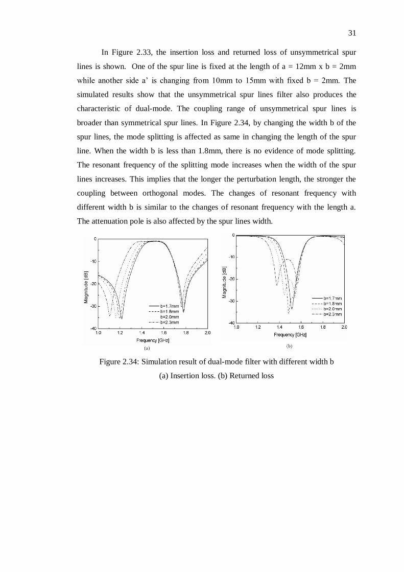
In Figure 2.33, the insertion loss and returned loss of unsymmetrical spur
lines is shown. One of the spur line is fixed at the length of a = 12mm x b = 2mm
while another side a‟ is changing from 10mm to 15mm with fixed b = 2mm. The
simulated results show that the unsymmetrical spur lines filter also produces the
characteristic of dual-mode. The coupling range of unsymmetrical spur lines is
broader than symmetrical spur lines. In Figure 2.34, by changing the width b of the
spur lines, the mode splitting is affected as same in changing the length of the spur
line. When the width b is less than 1.8mm, there is no evidence of mode splitting.
The resonant frequency of the splitting mode increases when the width of the spur
lines increases. This implies that the longer the perturbation length, the stronger the
coupling between orthogonal modes. The changes of resonant frequency with
different width b is similar to the changes of resonant frequency with the length a.
The attenuation pole is also affected by the spur lines width.
Figure 2.34: Simulation result of dual-mode filter with different width b
(a) Insertion loss. (b) Returned loss
32
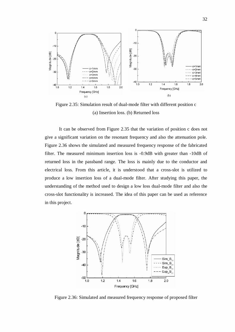
Figure 2.35: Simulation result of dual-mode filter with different position c
(a) Insertion loss. (b) Returned loss
It can be observed from Figure 2.35 that the variation of position c does not
give a significant variation on the resonant frequency and also the attenuation pole.
Figure 2.36 shows the simulated and measured frequency response of the fabricated
filter. The measured minimum insertion loss is -0.9dB with greater than -10dB of
returned loss in the passband range. The loss is mainly due to the conductor and
electrical loss. From this article, it is understood that a cross-slot is utilized to
produce a low insertion loss of a dual-mode filter. After studying this paper, the
understanding of the method used to design a low loss dual-mode filter and also the
cross-slot functionality is increased. The idea of this paper can be used as reference
in this project.
Figure 2.36: Simulated and measured frequency response of proposed filter
33
CHAPTER 3
3 MICROSTRIP PATCH BALUN BANDPASS FILTER
3.1 Background
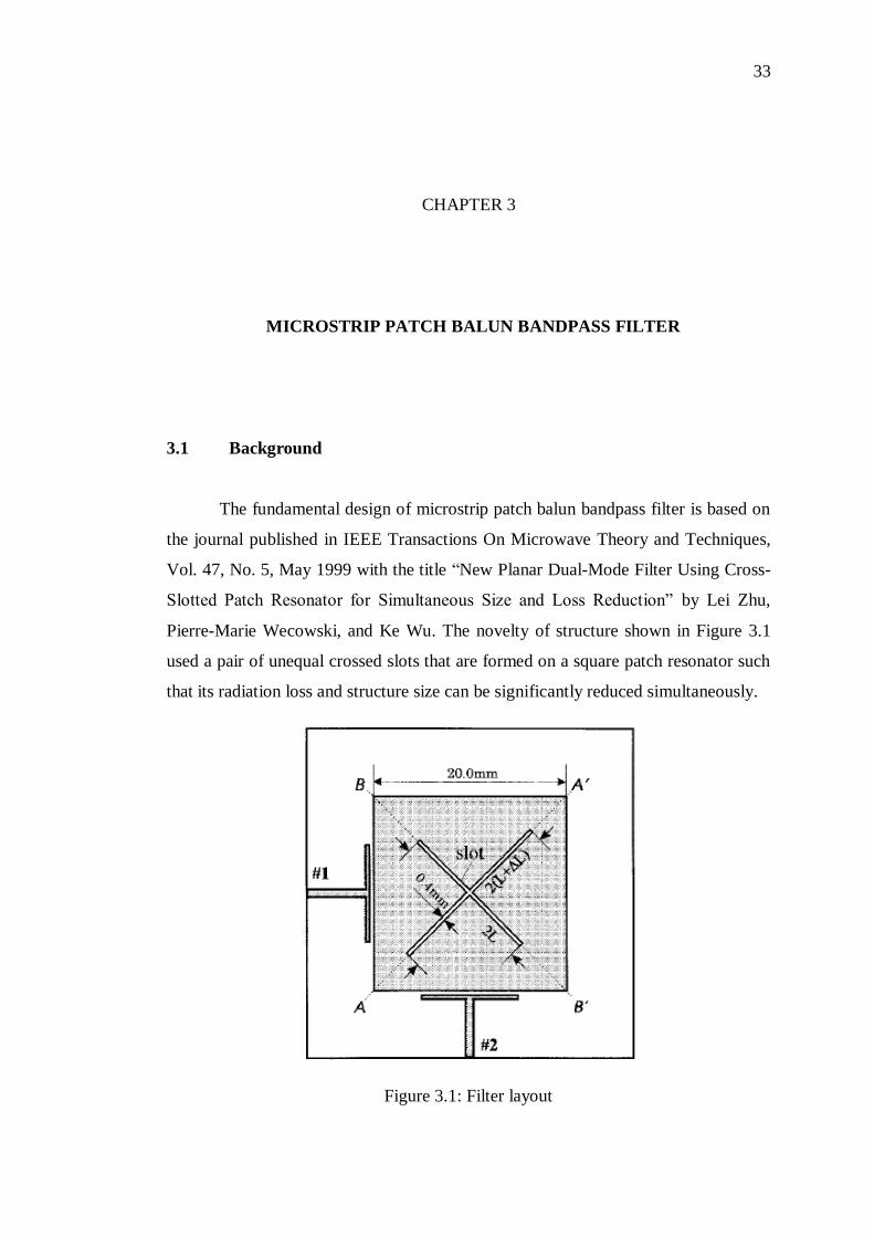
The fundamental design of microstrip patch balun bandpass filter is based on
the journal published in IEEE Transactions On Microwave Theory and Techniques,
Vol. 47, No. 5, May 1999 with the title “New Planar Dual-Mode Filter Using Cross-
Slotted Patch Resonator for Simultaneous Size and Loss Reduction” by Lei Zhu,
Pierre-Marie Wecowski, and Ke Wu. The novelty of structure shown in Figure 3.1
used a pair of unequal crossed slots that are formed on a square patch resonator such
that its radiation loss and structure size can be significantly reduced simultaneously.
Figure 3.1: Filter layout
34
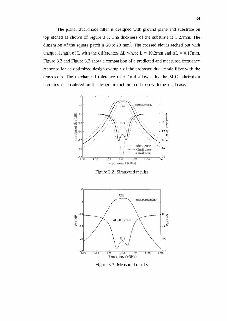
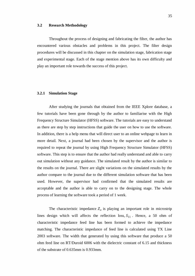
The planar dual-mode filter is designed with ground plane and substrate on
top etched as shown of Figure 3.1. The thickness of the substrate is 1.27mm. The
dimension of the square patch is 20 x 20 mm2. The crossed slot is etched out with
unequal length of L with the differences ∆L where L = 10.2mm and ∆L = 0.17mm.
Figure 3.2 and Figure 3.3 show a comparison of a predicted and measured frequency
response for an optimized design example of the proposed dual-mode filter with the
cross-slots. The mechanical tolerance of ± 1mil allowed by the MIC fabrication
facilities is considered for the design prediction in relation with the ideal case.
Figure 3.2: Simulated results
Figure 3.3: Measured results
35
3.2 Research Methodology
Throughout the process of designing and fabricating the filter, the author has
encountered various obstacles and problems in this project. The filter design
procedures will be discussed in this chapter on the simulation stage, fabrication stage
and experimental stage. Each of the stage mention above has its own difficulty and
play an important role towards the success of this project.
3.2.1 Simulation Stage
After studying the journals that obtained from the IEEE Xplore database, a
few tutorials have been gone through by the author to familiarise with the High
Frequency Structure Simulator (HFSS) software. The tutorials are easy to understand
as there are step by step instructions that guide the user on how to use the software.
In addition, there is a help menu that will direct user to an online webpage to learn in
more detail. Next, a journal had been chosen by the supervisor and the author is
required to repeat the journal by using High Frequency Structure Simulator (HFSS)
software. This step is to ensure that the author had really understand and able to carry
out simulation without any guidance. The simulated result by the author is similar to
the results on the journal. There are slight variations on the simulated results by the
author compare to the journal due to the different simulation software that has been
used. However, the supervisor had confirmed that the simulated results are
acceptable and the author is able to carry on to the designing stage. The whole
process of learning the software took a period of 1 week.
The characteristic impedance 𝑍𝑜 is playing an important role in microstrip
lines design which will affects the reflection loss, 𝑆11 . Hence, a 50 ohm of
characteristic impedance feed line has been formed to achieve the impedance
matching. The characteristic impedance of feed line is calculated using TX Line
2003 software. The width that generated by using this software that produce a 50
ohm feed line on RT/Duroid 6006 with the dielectric constant of 6.15 and thickness
of the substrate of 0.635mm is 0.933mm.
36
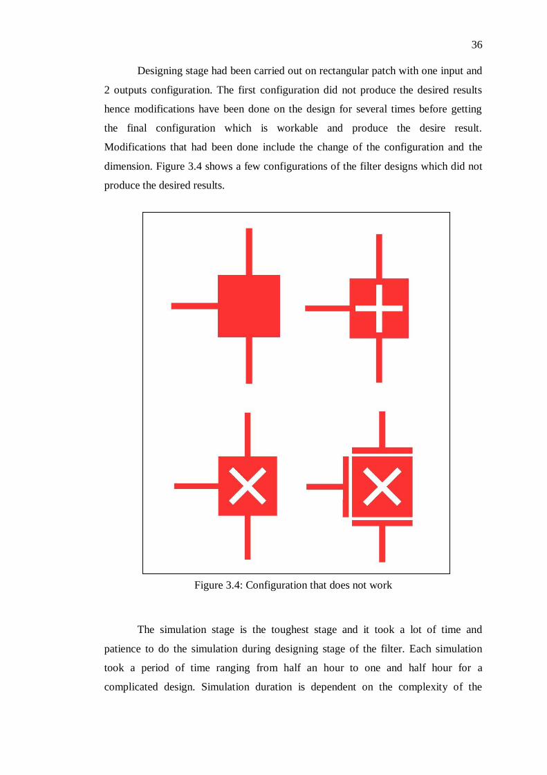
Designing stage had been carried out on rectangular patch with one input and
2 outputs configuration. The first configuration did not produce the desired results
hence modifications have been done on the design for several times before getting
the final configuration which is workable and produce the desire result.
Modifications that had been done include the change of the configuration and the
dimension. Figure 3.4 shows a few configurations of the filter designs which did not
produce the desired results.
Figure 3.4: Configuration that does not work
The simulation stage is the toughest stage and it took a lot of time and
patience to do the simulation during designing stage of the filter. Each simulation
took a period of time ranging from half an hour to one and half hour for a
complicated design. Simulation duration is dependent on the complexity of the
37
design and the computer processing speed. While waiting for the simulation results
to be done, the author did some analysis on previous results and modifications on the
design for next simulation. Modification and improvement can be easily done on the
design base on the analysis of previous results. The simulation stage took two
months to complete before going into the fabrication stage. Throughout the
simulation stage, perseverance and patience are very important to get the author keep
trying until a new filter design is successfully simulated with good performance.
3.2.2 Fabrication Stage
The optimized simulation results had been sent to the supervisor for
verification before the fabrication process start. RT/Duroid 6006 substrate is used to
fabricate the filter. RT/Duroid 6006 microwaves laminates are ceramic
polytetrafluoroethylene (PTFE) composites which are designed for electronic and
microwave circuit applications that require a high dielectric constant. PTFE is most
well known by the DuPont brand name Teflon. Moreover PTFE is
a fluorocarbon solid, as it is a high-molecular weight compound consisting only of
carbon and fluorine which make PTFE hydrophobic. This property of PTFE is
suitable for the fabrication process because during the fabrication, the substrate is
highly exposed to water. PTFE has one of the lowest coefficients of friction against
any solid.
RT/Duroid 6006 is available with dielectric constant value of 6.15. In
addition, RT/Duroid 6006 features ease of fabrication and stability in use. It might
have tight dielectric constant and thickness control, low moisture absorption and
good thermal mechanical stability. RT/Duroid 6006 laminates are supplied with clad
both sides ¼ oz to 2 oz / ft2 (9 to 70 µm) electrodeposited copper foil.
The first step of the fabrication process is to draw the filter design
configuration with exact dimension using Easily Applicable Graphical Layout Editor
(EAGLE) software from CadSoft. The size of filter that printed out must be 100%
38
exactly of the size of the simulation filter design. The gap for capacitive coupling is
extremely sensitive for this design. A 0.01mm mismatch may affect the final result
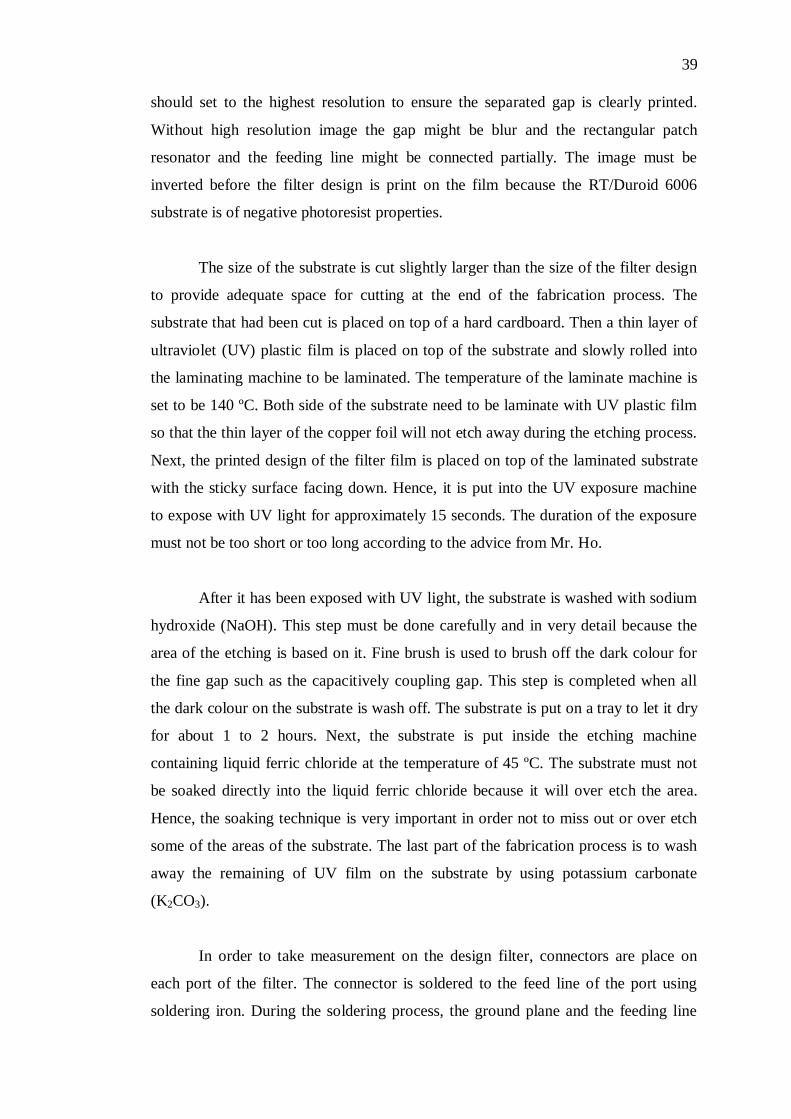
tremendously. Next, the ready design is printed on a special waterproof inkjet film
shown in Figure 3.5. The film has different types of surface on both sides where one
side of the surface is smooth while the other side has a sticky surface. The design
must be printed on the sticky surface and must avoid touching the area of the printed
design. An example of the printed design on the film is shown in Figure 3.6.
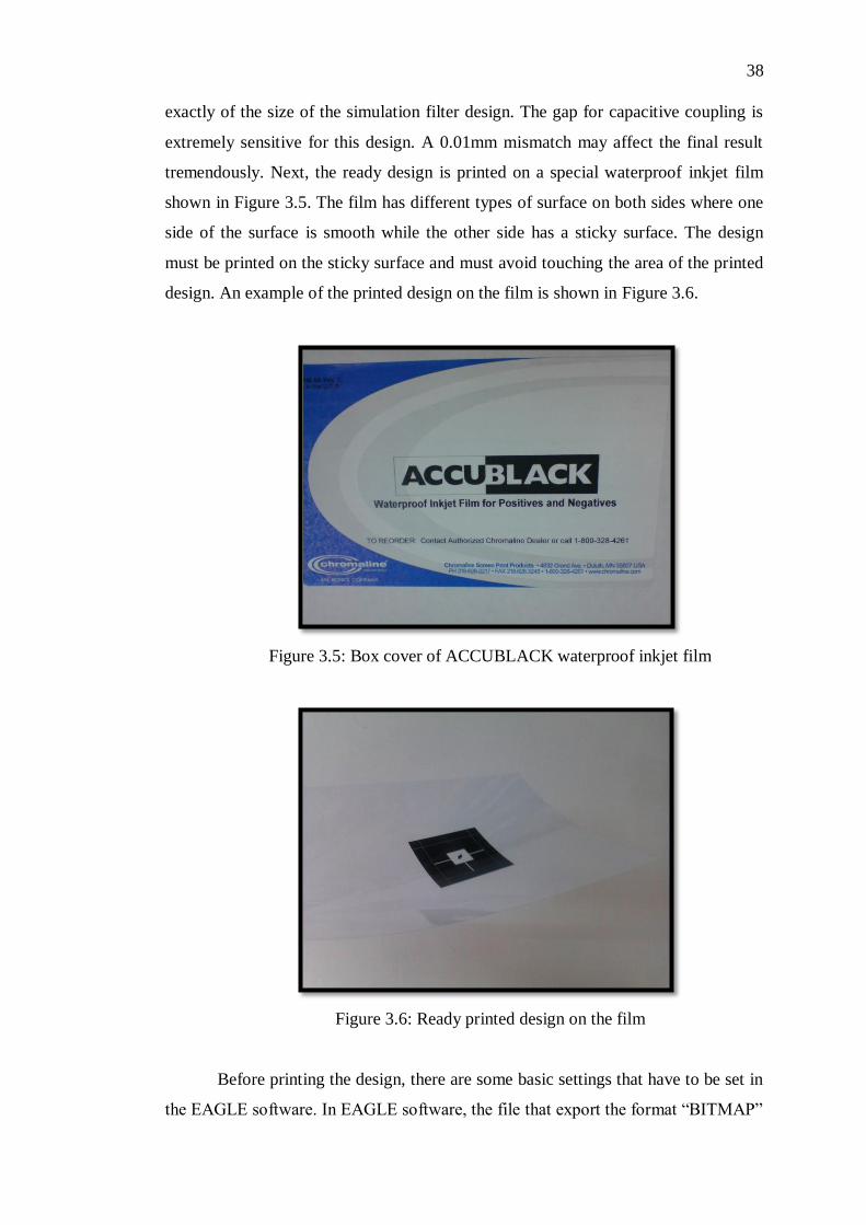
Figure 3.5: Box cover of ACCUBLACK waterproof inkjet film
Figure 3.6: Ready printed design on the film
Before printing the design, there are some basic settings that have to be set in
the EAGLE software. In EAGLE software, the file that export the format “BITMAP”
39
should set to the highest resolution to ensure the separated gap is clearly printed.
Without high resolution image the gap might be blur and the rectangular patch
resonator and the feeding line might be connected partially. The image must be
inverted before the filter design is print on the film because the RT/Duroid 6006
substrate is of negative photoresist properties.
The size of the substrate is cut slightly larger than the size of the filter design
to provide adequate space for cutting at the end of the fabrication process. The
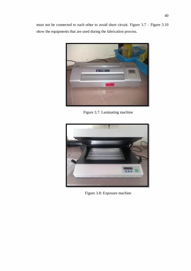
substrate that had been cut is placed on top of a hard cardboard. Then a thin layer of
ultraviolet (UV) plastic film is placed on top of the substrate and slowly rolled into
the laminating machine to be laminated. The temperature of the laminate machine is
set to be 140 ºC. Both side of the substrate need to be laminate with UV plastic film
so that the thin layer of the copper foil will not etch away during the etching process.
Next, the printed design of the filter film is placed on top of the laminated substrate
with the sticky surface facing down. Hence, it is put into the UV exposure machine
to expose with UV light for approximately 15 seconds. The duration of the exposure
must not be too short or too long according to the advice from Mr. Ho.
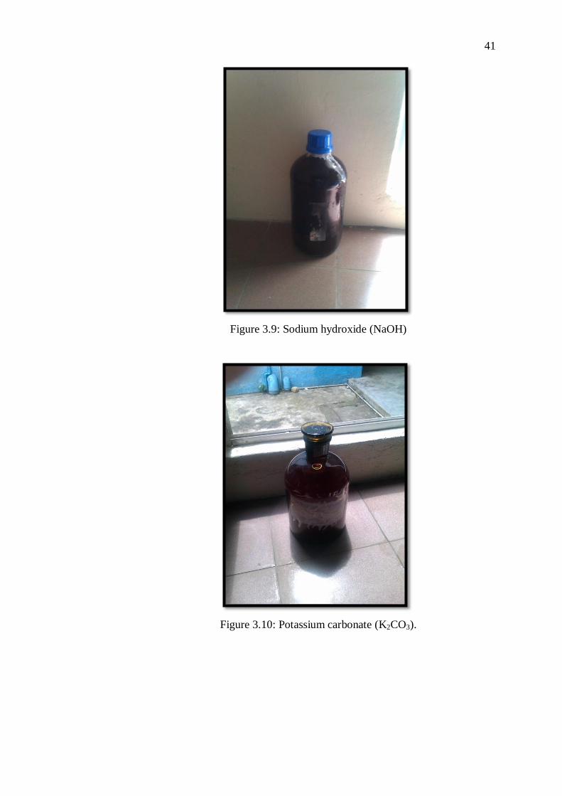
After it has been exposed with UV light, the substrate is washed with sodium
hydroxide (NaOH). This step must be done carefully and in very detail because the
area of the etching is based on it. Fine brush is used to brush off the dark colour for
the fine gap such as the capacitively coupling gap. This step is completed when all
the dark colour on the substrate is wash off. The substrate is put on a tray to let it dry
for about 1 to 2 hours. Next, the substrate is put inside the etching machine
containing liquid ferric chloride at the temperature of 45 ºC. The substrate must not
be soaked directly into the liquid ferric chloride because it will over etch the area.
Hence, the soaking technique is very important in order not to miss out or over etch
some of the areas of the substrate. The last part of the fabrication process is to wash
away the remaining of UV film on the substrate by using potassium carbonate
(K2CO3).
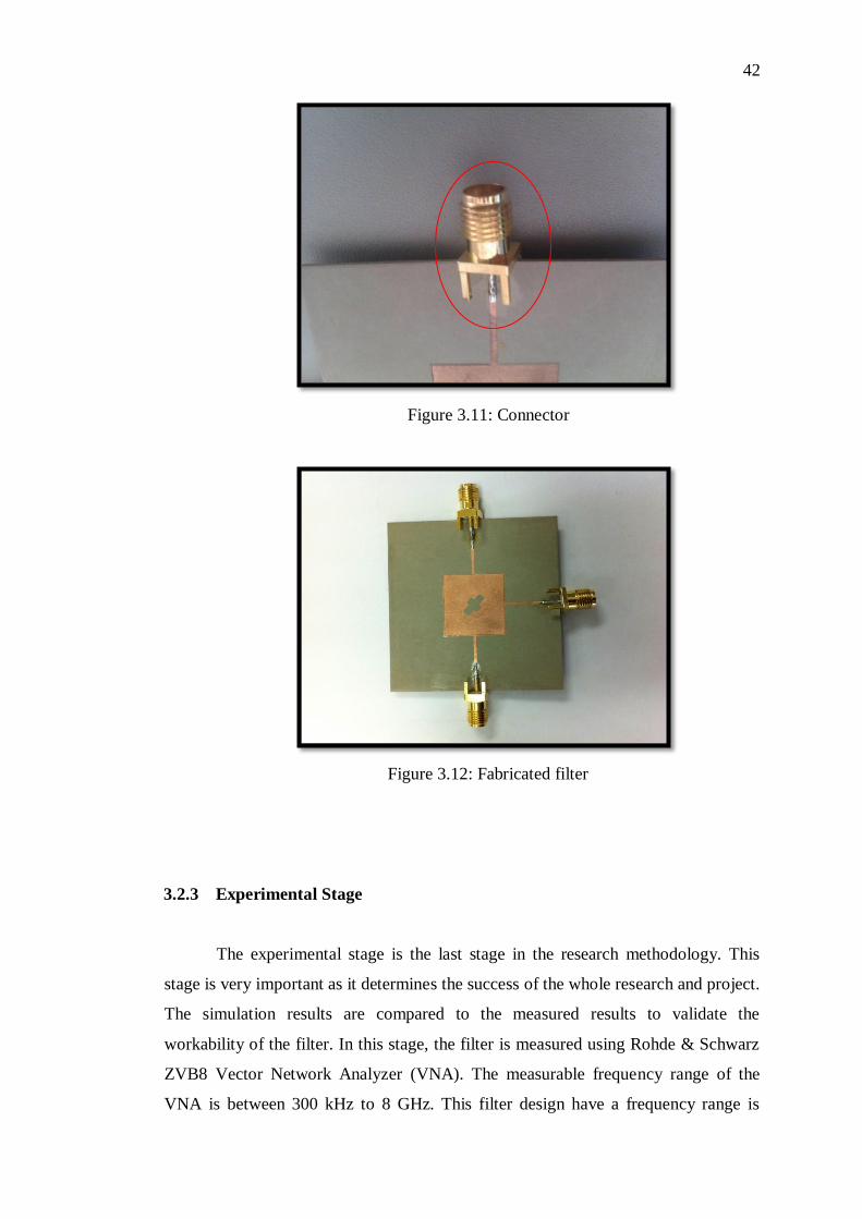
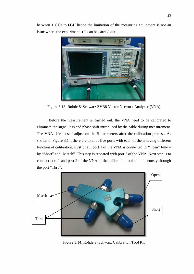
In order to take measurement on the design filter, connectors are place on
each port of the filter. The connector is soldered to the feed line of the port using
soldering iron. During the soldering process, the ground plane and the feeding line
40
must not be connected to each other to avoid short circuit. Figure 3.7 – Figure 3.10
show the equipments that are used during the fabrication process.
Figure 3.7: Laminating machine
Figure 3.8: Exposure machine
41
Figure 3.9: Sodium hydroxide (NaOH)
Figure 3.10: Potassium carbonate (K2CO3).
42
Figure 3.11: Connector
Figure 3.12: Fabricated filter
3.2.3 Experimental Stage
The experimental stage is the last stage in the research methodology. This
stage is very important as it determines the success of the whole research and project.
The simulation results are compared to the measured results to validate the
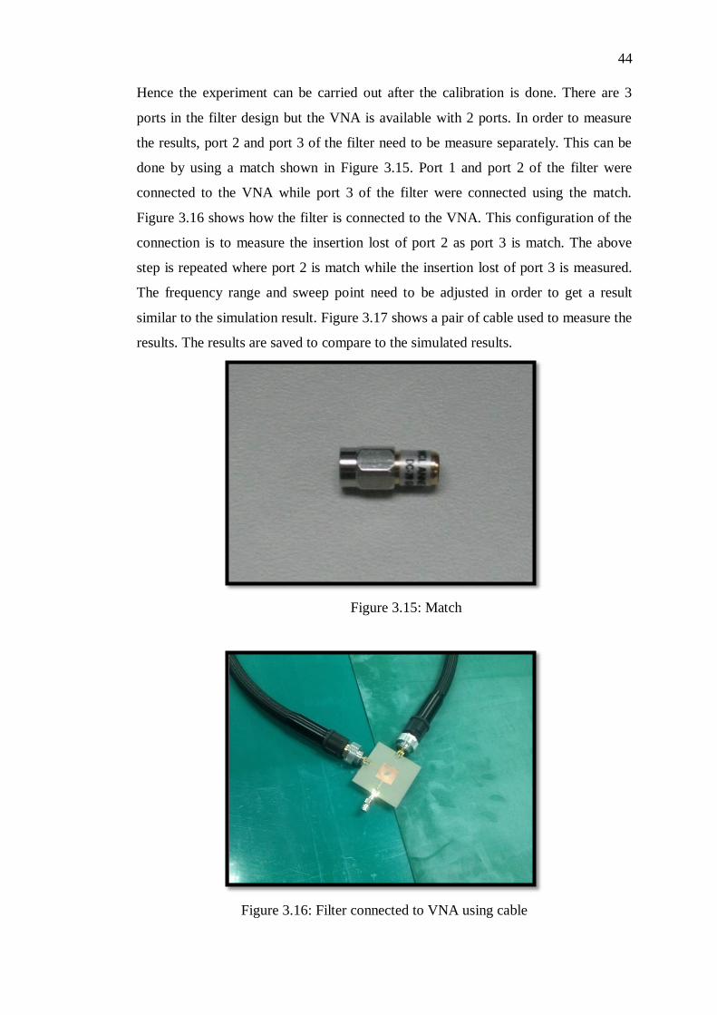
workability of the filter. In this stage, the filter is measured using Rohde & Schwarz
ZVB8 Vector Network Analyzer (VNA). The measurable frequency range of the
VNA is between 300 kHz to 8 GHz. This filter design have a frequency range is
43
between 1 GHz to 6GH hence the limitation of the measuring equipment is not an
issue where the experiment still can be carried out.
Figure 3.13: Rohde & Schwarz ZVB8 Vector Network Analyzer (VNA)
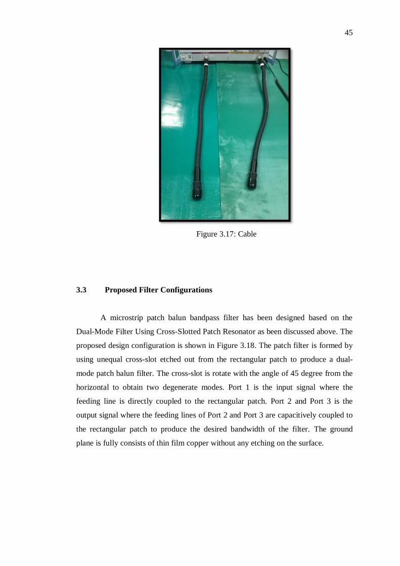
Before the measurement is carried out, the VNA need to be calibrated to
eliminate the signal loss and phase shift introduced by the cable during measurement.
The VNA able to self adjust on the S-parameters after the calibration process. As
shown in Figure 3.14, there are total of five ports with each of them having different
function of calibration. First of all, port 1 of the VNA is connected to “Open” follow
by “Short” and “Match”. This step is repeated with port 2 of the VNA. Next step is to
connect port 1 and port 2 of the VNA to the calibration tool simultaneously through
the port “Thru”.
Figure 3.14: Rohde & Schwarz Calibration Tool Kit
Open
Short
Thru
Match
44
Hence the experiment can be carried out after the calibration is done. There are 3
ports in the filter design but the VNA is available with 2 ports. In order to measure
the results, port 2 and port 3 of the filter need to be measure separately. This can be
done by using a match shown in Figure 3.15. Port 1 and port 2 of the filter were
connected to the VNA while port 3 of the filter were connected using the match.
Figure 3.16 shows how the filter is connected to the VNA. This configuration of the
connection is to measure the insertion lost of port 2 as port 3 is match. The above
step is repeated where port 2 is match while the insertion lost of port 3 is measured.
The frequency range and sweep point need to be adjusted in order to get a result
similar to the simulation result. Figure 3.17 shows a pair of cable used to measure the
results. The results are saved to compare to the simulated results.
Figure 3.15: Match
Figure 3.16: Filter connected to VNA using cable
45
Figure 3.17: Cable
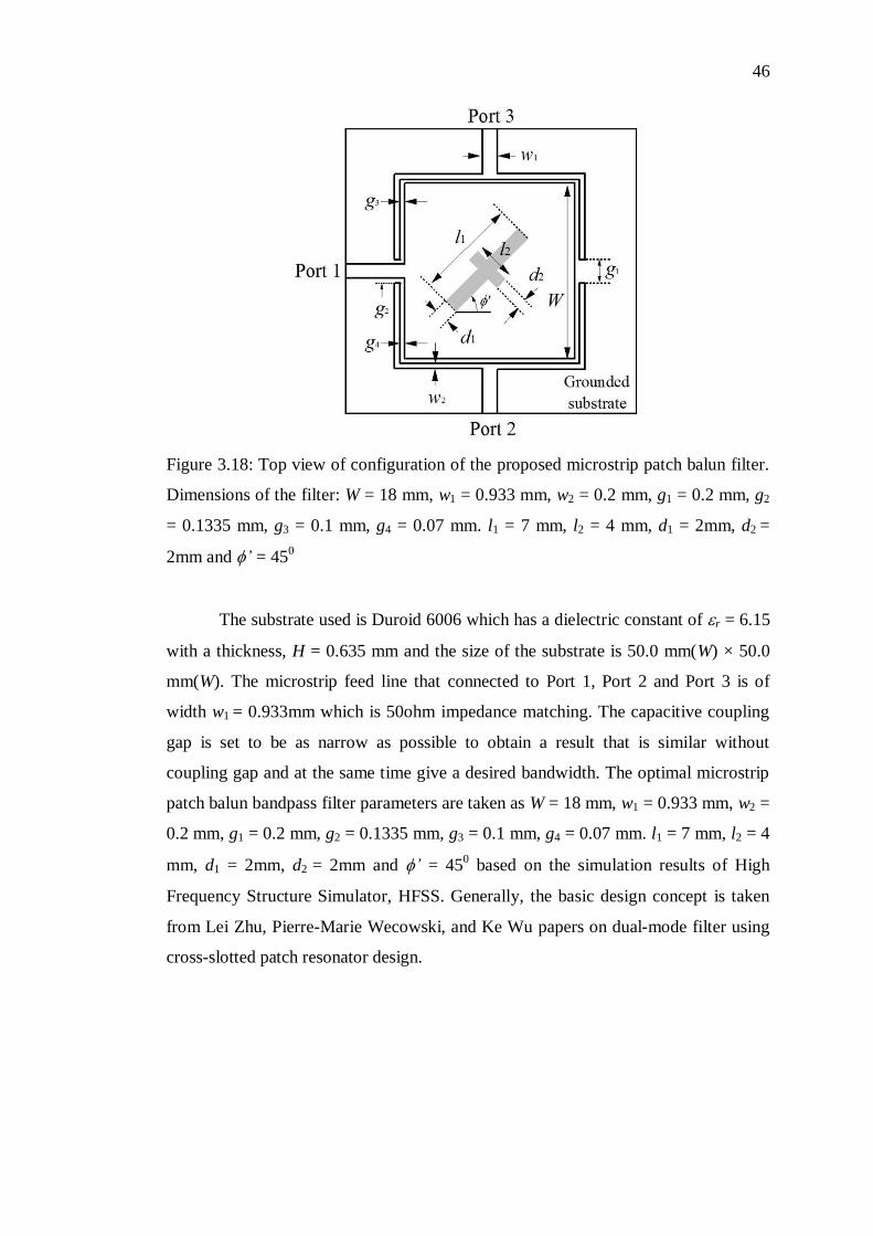
3.3 Proposed Filter Configurations
A microstrip patch balun bandpass filter has been designed based on the
Dual-Mode Filter Using Cross-Slotted Patch Resonator as been discussed above. The
proposed design configuration is shown in Figure 3.18. The patch filter is formed by
using unequal cross-slot etched out from the rectangular patch to produce a dual-
mode patch balun filter. The cross-slot is rotate with the angle of 45 degree from the
horizontal to obtain two degenerate modes. Port 1 is the input signal where the
feeding line is directly coupled to the rectangular patch. Port 2 and Port 3 is the
output signal where the feeding lines of Port 2 and Port 3 are capacitively coupled to
the rectangular patch to produce the desired bandwidth of the filter. The ground
plane is fully consists of thin film copper without any etching on the surface.
46
Figure 3.18: Top view of configuration of the proposed microstrip patch balun filter.
Dimensions of the filter: W = 18 mm, w1 = 0.933 mm, w2 = 0.2 mm, g1 = 0.2 mm, g2
= 0.1335 mm, g3 = 0.1 mm, g4 = 0.07 mm. l1 = 7 mm, l2 = 4 mm, d1 = 2mm, d2 =
2mm and ’ = 450
The substrate used is Duroid 6006 which has a dielectric constant of r = 6.15
with a thickness, H = 0.635 mm and the size of the substrate is 50.0 mm(W) × 50.0
mm(W). The microstrip feed line that connected to Port 1, Port 2 and Port 3 is of
width w1 = 0.933mm which is 50ohm impedance matching. The capacitive coupling
gap is set to be as narrow as possible to obtain a result that is similar without
coupling gap and at the same time give a desired bandwidth. The optimal microstrip
patch balun bandpass filter parameters are taken as W = 18 mm, w1 = 0.933 mm, w2 =
0.2 mm, g1 = 0.2 mm, g2 = 0.1335 mm, g3 = 0.1 mm, g4 = 0.07 mm. l1 = 7 mm, l2 = 4
mm, d1 = 2mm, d2 = 2mm and ’ = 450 based on the simulation results of High
Frequency Structure Simulator, HFSS. Generally, the basic design concept is taken
from Lei Zhu, Pierre-Marie Wecowski, and Ke Wu papers on dual-mode filter using
cross-slotted patch resonator design.

47
47
CHAPTER 4
4 RESULTS AND DISCUSSIONS
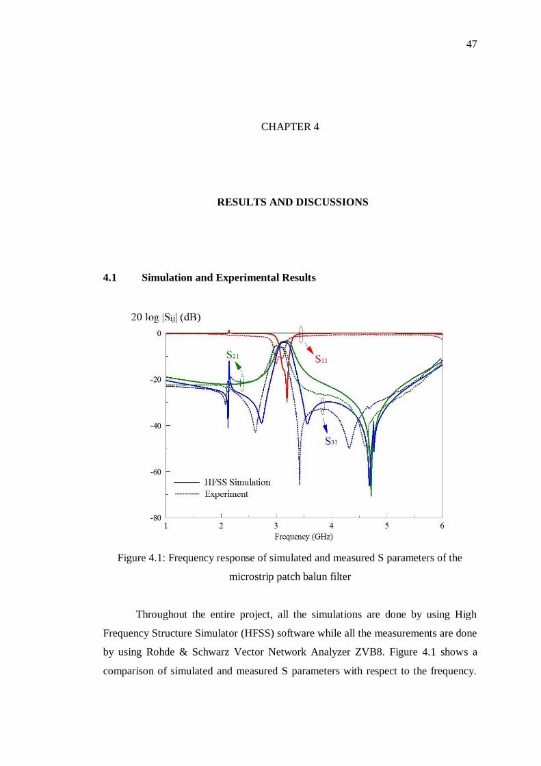
4.1 Simulation and Experimental Results
Figure 4.1: Frequency response of simulated and measured S parameters of the
microstrip patch balun filter
Throughout the entire project, all the simulations are done by using High
Frequency Structure Simulator (HFSS) software while all the measurements are done
by using Rohde & Schwarz Vector Network Analyzer ZVB8. Figure 4.1 shows a
comparison of simulated and measured S parameters with respect to the frequency.
48
This frequency response of S parameters not only shows that the filter is a bandpass
filter but also function as a balun at the same time.
With reference to Figure 4.1, a reasonable good agreement is found in
between the simulated and measured frequency response. The passband center
frequency of both S21 and S31 is at 3.05 Ghz with passband covering between 2.91 –
3.19 GHz. Two transmission zeroes are also observed in S31 near to the filter
passband. On the other hand the output signal magnitudes |S21| and |S31| are equal and
read at -6 dB. This might due to additional losses that introduced by the connectors
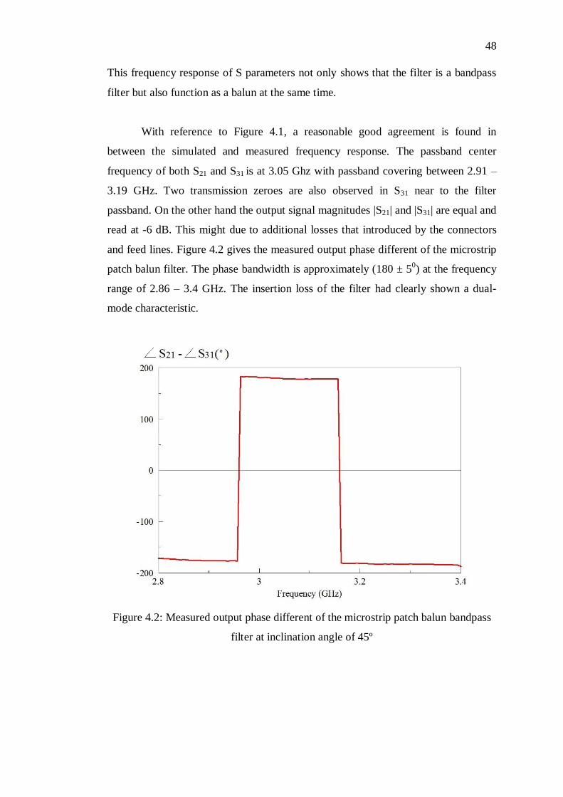
and feed lines. Figure 4.2 gives the measured output phase different of the microstrip
patch balun filter. The phase bandwidth is approximately (180 ± 50) at the frequency
range of 2.86 – 3.4 GHz. The insertion loss of the filter had clearly shown a dual-
mode characteristic.
Figure 4.2: Measured output phase different of the microstrip patch balun bandpass
filter at inclination angle of 45º
49
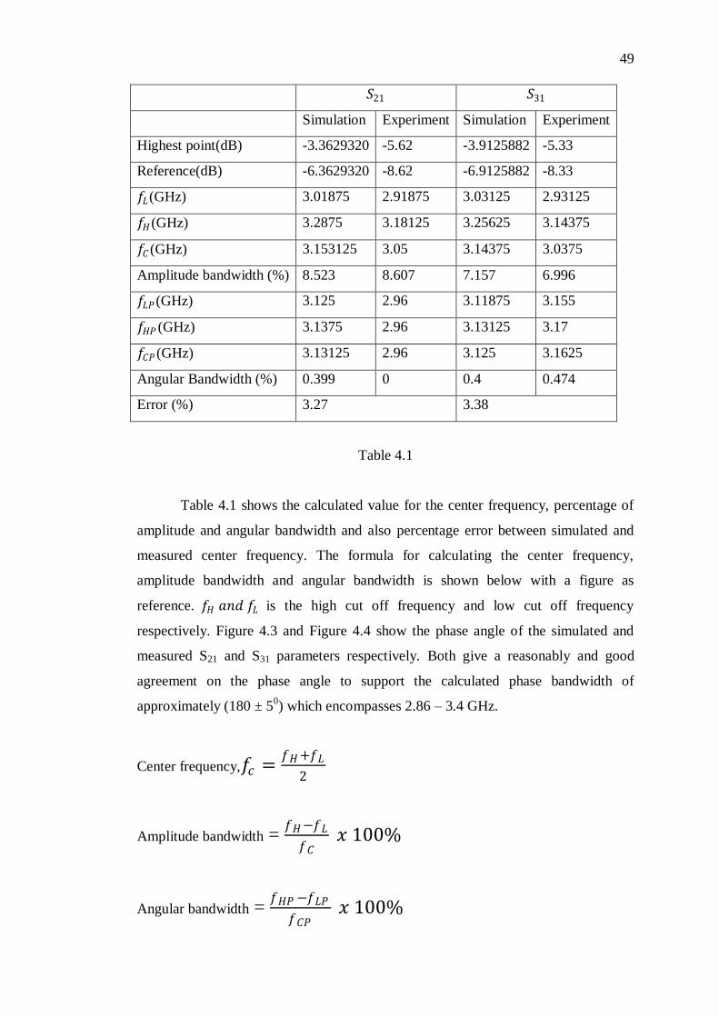
𝑆21 𝑆31
Simulation Experiment Simulation Experiment
Highest point(dB) -3.3629320 -5.62 -3.9125882 -5.33
Reference(dB) -6.3629320 -8.62 -6.9125882 -8.33
𝑓𝐿(GHz) 3.01875 2.91875 3.03125 2.93125
𝑓𝐻(GHz) 3.2875 3.18125 3.25625 3.14375
𝑓𝐶 (GHz) 3.153125 3.05 3.14375 3.0375
Amplitude bandwidth (%) 8.523 8.607 7.157 6.996
𝑓𝐿𝑃 (GHz) 3.125 2.96 3.11875 3.155
𝑓𝐻𝑃 (GHz) 3.1375 2.96 3.13125 3.17
𝑓𝐶𝑃 (GHz) 3.13125 2.96 3.125 3.1625
Angular Bandwidth (%) 0.399 0 0.4 0.474
Error (%) 3.27 3.38
Table 4.1
Table 4.1 shows the calculated value for the center frequency, percentage of
amplitude and angular bandwidth and also percentage error between simulated and
measured center frequency. The formula for calculating the center frequency,
amplitude bandwidth and angular bandwidth is shown below with a figure as
reference. 𝑓𝐻 𝑎𝑛𝑑 𝑓𝐿 is the high cut off frequency and low cut off frequency
respectively. Figure 4.3 and Figure 4.4 show the phase angle of the simulated and
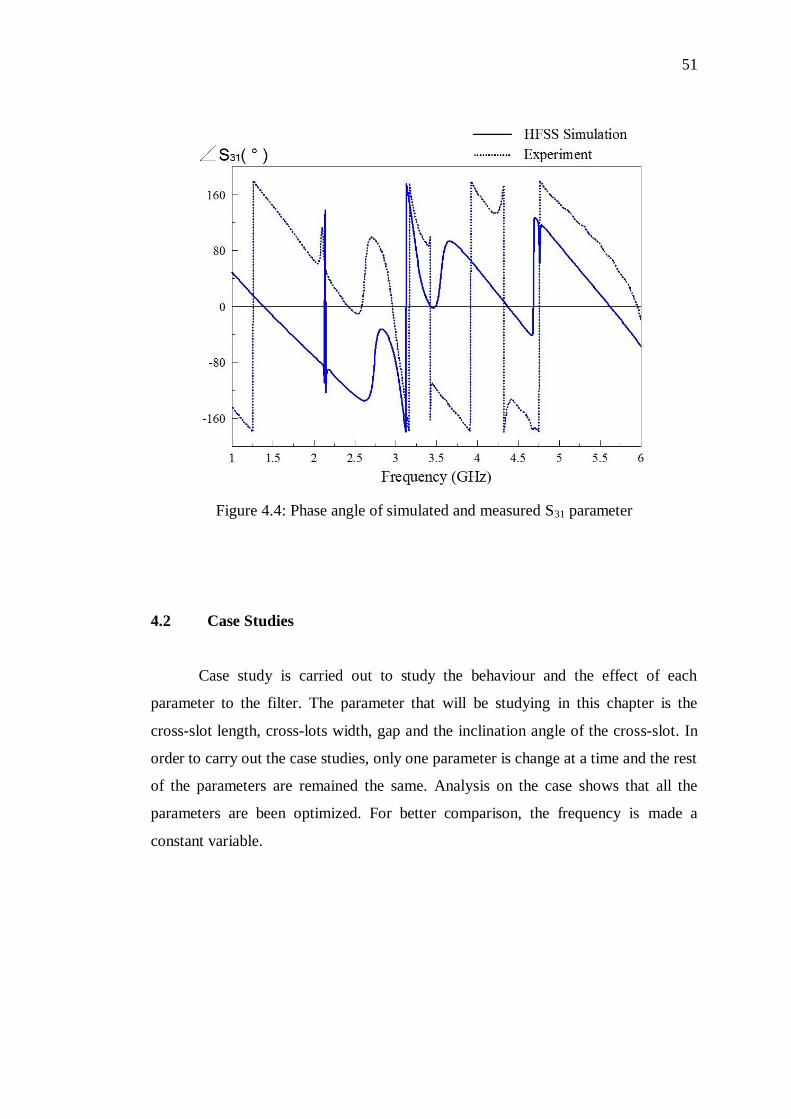
measured S21 and S31 parameters respectively. Both give a reasonably and good
agreement on the phase angle to support the calculated phase bandwidth of
approximately (180 ± 50) which encompasses 2.86 – 3.4 GHz.
Center frequency,𝑓𝑐 =𝑓𝐻+𝑓𝐿
2
Amplitude bandwidth = 𝑓𝐻−𝑓𝐿
𝑓𝐶 𝑥 100%
Angular bandwidth = 𝑓𝐻𝑃 −𝑓𝐿𝑃
𝑓𝐶𝑃 𝑥 100%

50
Error = 𝑓𝑐(𝑠𝑖𝑚𝑢𝑙𝑎𝑡𝑒𝑑 )−𝑓𝑐(𝑒𝑥𝑝𝑒𝑟𝑖𝑚𝑒𝑛𝑡 )
𝑓𝑐(𝑠𝑖𝑚𝑢𝑙𝑎𝑡𝑒𝑑 ) 𝑥 100%
Figure 4.3: Phase angle of simulated and measure S21 parameter
-5.62dB -8.62dB
-5.62dB
-8.62dB FL FH
Fc
51
Figure 4.4: Phase angle of simulated and measured S31 parameter
4.2 Case Studies
Case study is carried out to study the behaviour and the effect of each
parameter to the filter. The parameter that will be studying in this chapter is the
cross-slot length, cross-lots width, gap and the inclination angle of the cross-slot. In
order to carry out the case studies, only one parameter is change at a time and the rest
of the parameters are remained the same. Analysis on the case shows that all the
parameters are been optimized. For better comparison, the frequency is made a
constant variable.
52
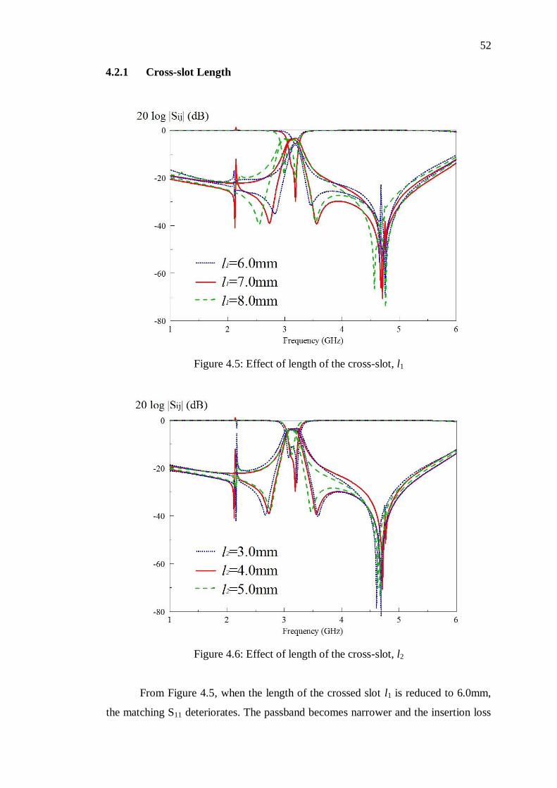
4.2.1 Cross-slot Length
Figure 4.5: Effect of length of the cross-slot, l1
Figure 4.6: Effect of length of the cross-slot, l2
From Figure 4.5, when the length of the crossed slot l1 is reduced to 6.0mm,
the matching S11 deteriorates. The passband becomes narrower and the insertion loss

53
is reduced from -3dB to -6dB. When the length is increased to 8.0mm, the return loss
is more than – 10dB. Both of the modes do not combine well in the passband. Even
though the dual-mode characteristic can be seen clearly, it does not produce good
results. From Figure 4.6, when the length l2 is reduced to 3.0mm, an additional mode
is generated near to the 2GHz frequency. Both of the modes do not combine well in
the passband. When it is 5.00mm the two modes merged well and cannot be seen
from the figure.
4.2.2 Cross-slots Width
Figure 4.7: Effect of width of the cross-slot, d1
54
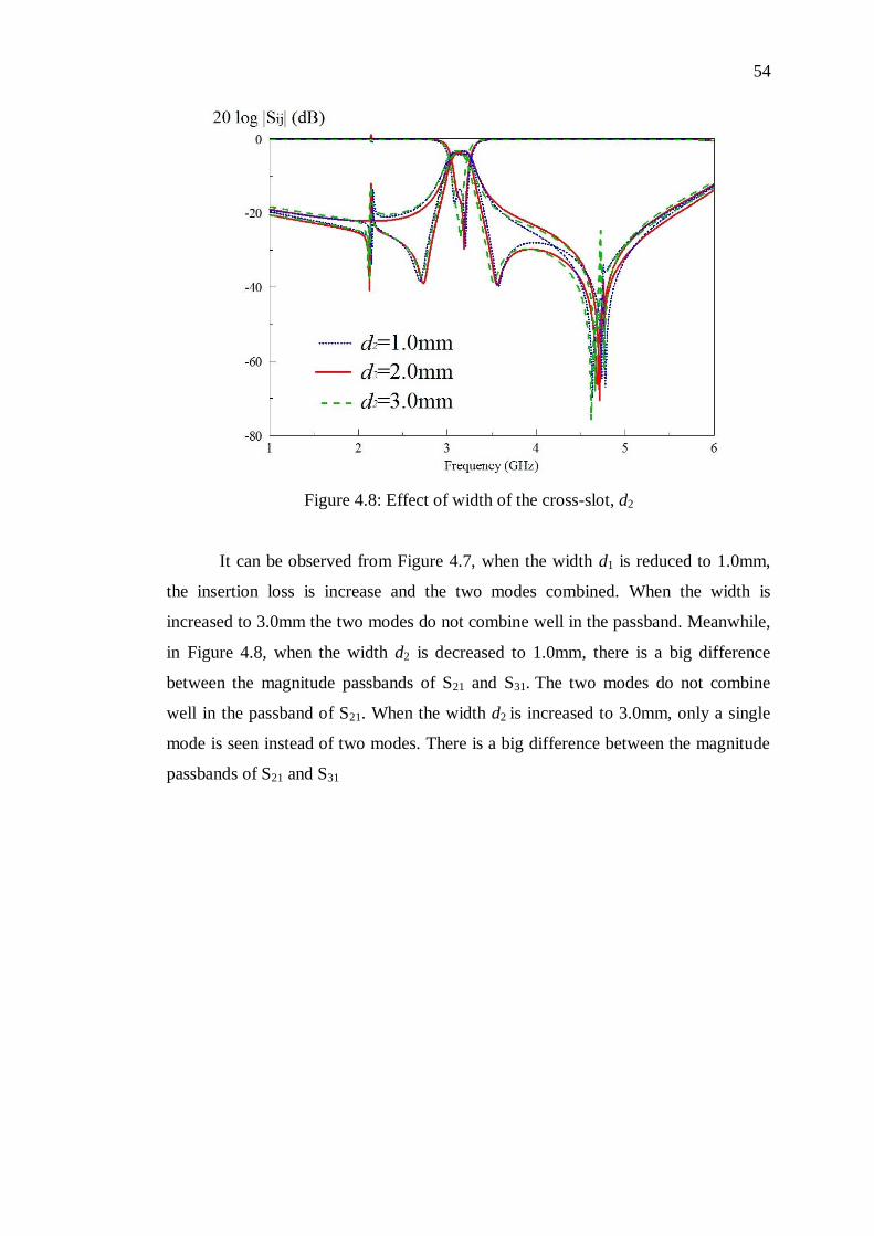
Figure 4.8: Effect of width of the cross-slot, d2
It can be observed from Figure 4.7, when the width d1 is reduced to 1.0mm,
the insertion loss is increase and the two modes combined. When the width is
increased to 3.0mm the two modes do not combine well in the passband. Meanwhile,
in Figure 4.8, when the width d2 is decreased to 1.0mm, there is a big difference
between the magnitude passbands of S21 and S31. The two modes do not combine
well in the passband of S21. When the width d2 is increased to 3.0mm, only a single
mode is seen instead of two modes. There is a big difference between the magnitude
passbands of S21 and S31
55
4.2.3 Gap
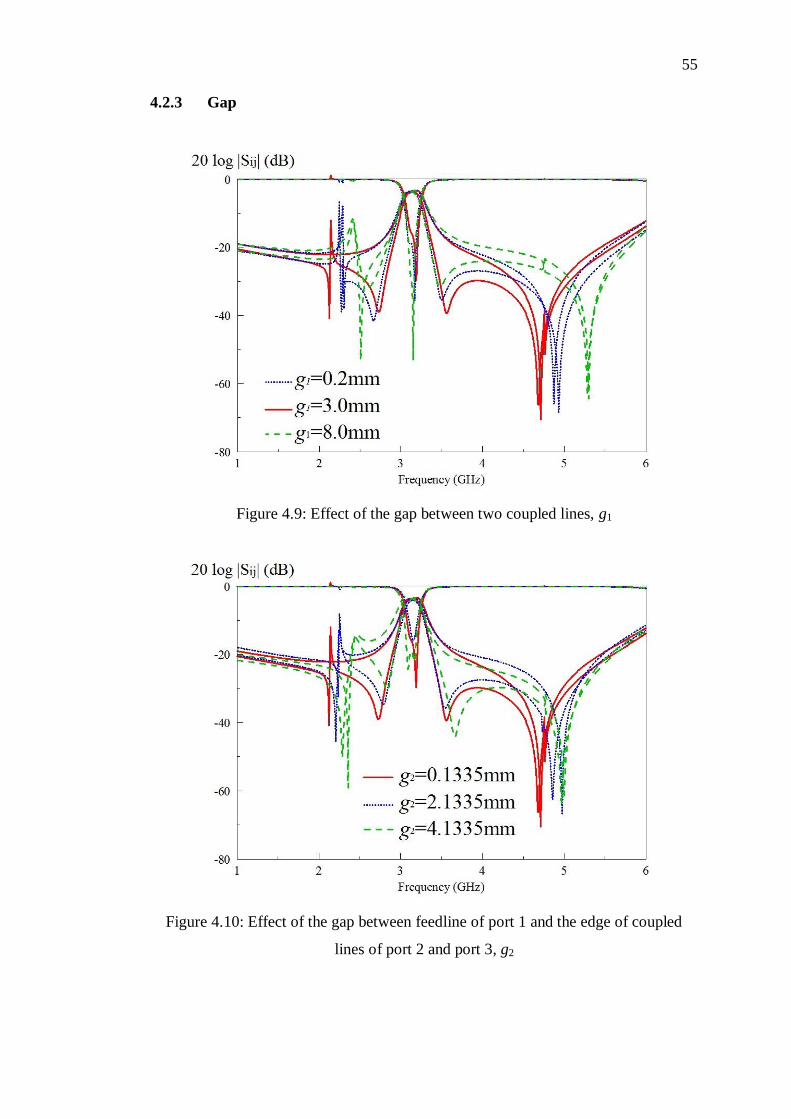
Figure 4.9: Effect of the gap between two coupled lines, g1
Figure 4.10: Effect of the gap between feedline of port 1 and the edge of coupled
lines of port 2 and port 3, g2
56
Figure 4.11: Effect of the coupled line with the rectangular patch, g3
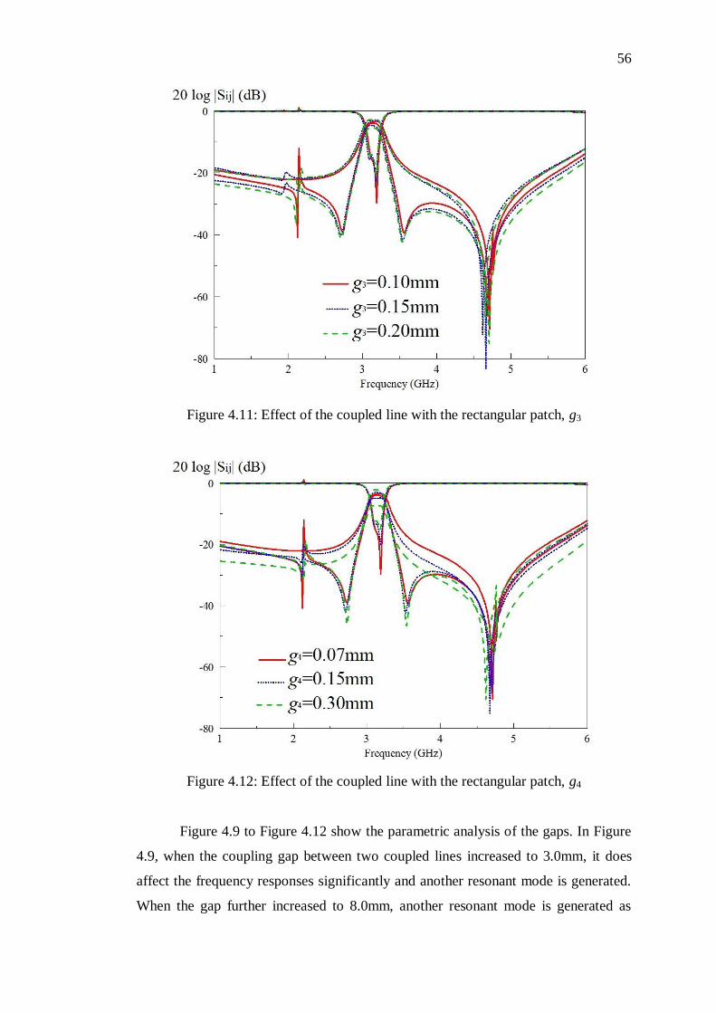
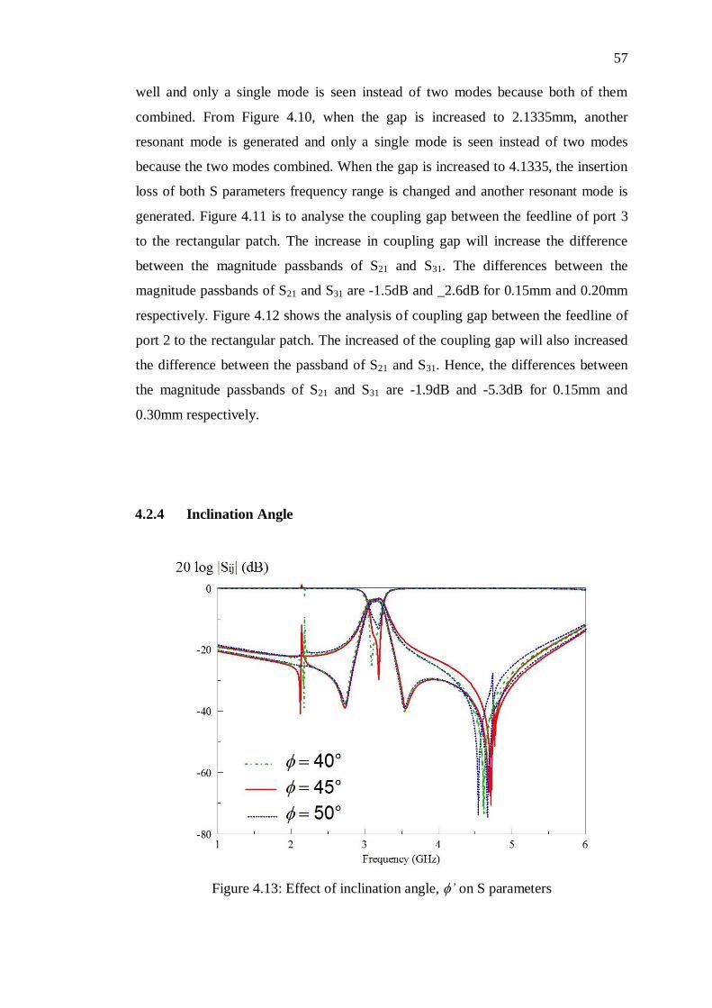
Figure 4.12: Effect of the coupled line with the rectangular patch, g4
Figure 4.9 to Figure 4.12 show the parametric analysis of the gaps. In Figure
4.9, when the coupling gap between two coupled lines increased to 3.0mm, it does
affect the frequency responses significantly and another resonant mode is generated.
When the gap further increased to 8.0mm, another resonant mode is generated as
57
well and only a single mode is seen instead of two modes because both of them
combined. From Figure 4.10, when the gap is increased to 2.1335mm, another
resonant mode is generated and only a single mode is seen instead of two modes
because the two modes combined. When the gap is increased to 4.1335, the insertion
loss of both S parameters frequency range is changed and another resonant mode is
generated. Figure 4.11 is to analyse the coupling gap between the feedline of port 3
to the rectangular patch. The increase in coupling gap will increase the difference
between the magnitude passbands of S21 and S31. The differences between the
magnitude passbands of S21 and S31 are -1.5dB and _2.6dB for 0.15mm and 0.20mm
respectively. Figure 4.12 shows the analysis of coupling gap between the feedline of
port 2 to the rectangular patch. The increased of the coupling gap will also increased
the difference between the passband of S21 and S31. Hence, the differences between
the magnitude passbands of S21 and S31 are -1.9dB and -5.3dB for 0.15mm and
0.30mm respectively.
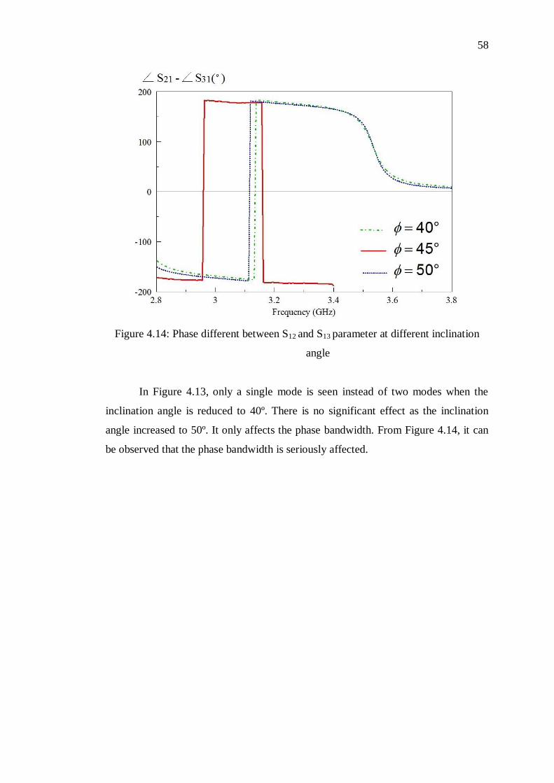
4.2.4 Inclination Angle
Figure 4.13: Effect of inclination angle, ’ on S parameters
58
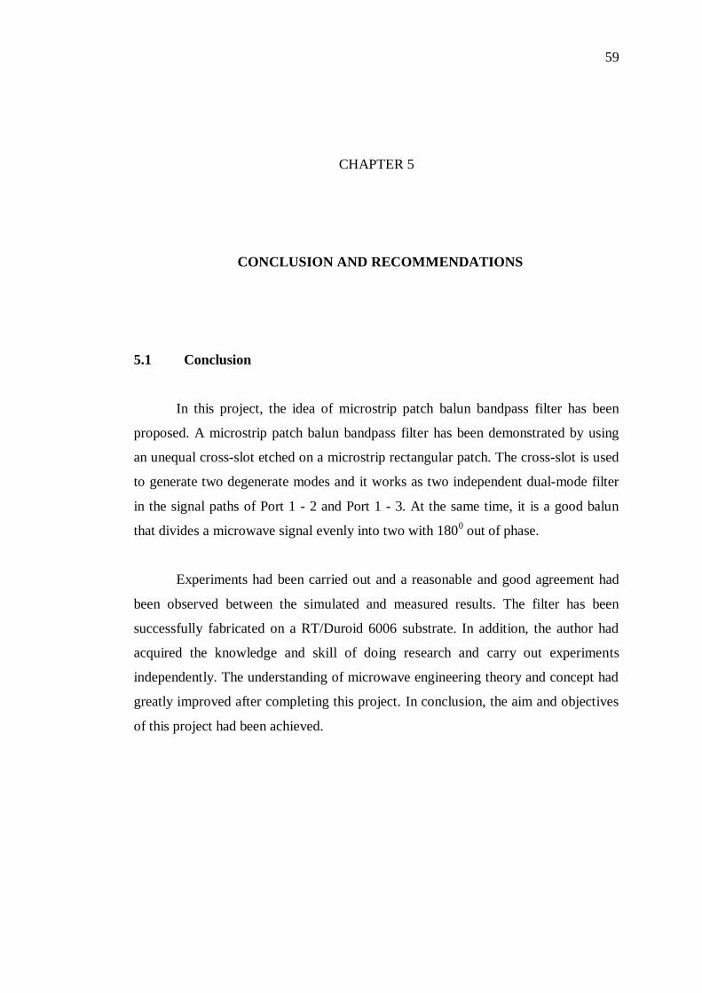
Figure 4.14: Phase different between S12 and S13 parameter at different inclination
angle
In Figure 4.13, only a single mode is seen instead of two modes when the
inclination angle is reduced to 40º. There is no significant effect as the inclination
angle increased to 50º. It only affects the phase bandwidth. From Figure 4.14, it can
be observed that the phase bandwidth is seriously affected.
59
CHAPTER 5
5 CONCLUSION AND RECOMMENDATIONS
5.1 Conclusion
In this project, the idea of microstrip patch balun bandpass filter has been
proposed. A microstrip patch balun bandpass filter has been demonstrated by using
an unequal cross-slot etched on a microstrip rectangular patch. The cross-slot is used
to generate two degenerate modes and it works as two independent dual-mode filter
in the signal paths of Port 1 - 2 and Port 1 - 3. At the same time, it is a good balun
that divides a microwave signal evenly into two with 1800 out of phase.
Experiments had been carried out and a reasonable and good agreement had
been observed between the simulated and measured results. The filter has been
successfully fabricated on a RT/Duroid 6006 substrate. In addition, the author had
acquired the knowledge and skill of doing research and carry out experiments
independently. The understanding of microwave engineering theory and concept had
greatly improved after completing this project. In conclusion, the aim and objectives
of this project had been achieved.
60
5.2 Recommendation
The proposed microstrip patch balun filter can be further improved where the
capacitive coupled feed lines gap can be further decrease. However this is unable to
be done in the laboratory due to lack of technology on fabricating the filter. Only
high technology which uses laser light to etch the microstrip line will able to produce
a fine narrow line up to 0.02mm. Narrower coupled feed lines can increase the
insertion lost to exactly –3dB. Moreover, a multilayer approach can be incorporated
into the proposed patch balun filter to produce a multilayer balun filter. This
approach is difficult to design as it needs a high dielectric constant substrate for both
layers so that the signal can be go through from bottom layer to the top layer.
RT/Duroid 6010 substrate has high dielectric constant but it is expensive and will
produce high radiation loss. Hence, further research need to be done on this area to
make this idea successful in the future.
The proposed balun filter/power divider only can divide one microwave
signal equally into two. Hence, in future more output can be design on the filter
where one microwave signal can be divided into several output equally with same
magnitude. This will be a new research area for microwave filter. In conclusion,
there are still many areas on microwave engineering that need further research into to
produce more filter with good features and contribute to wireless communication
development.
61
REFERENCES
Band Pass Filter. (n.d.) Wikipedia. Retrieved March, 2011 from
http://en.wikipedia.org/wiki/Band_pass_filter
Microstrip-Microwave Encyclopedia. (20,August 2010). Retrieved March 2011,
from microwaves101.com:
http://www.microwaves101.com/encyclopedia/microstrip.cfm
Zhu Lei, Pierre-Marie Wecowski, and Ke Wu, “New Planar Dual-Mode Filter Using
Cross-Slotted Patch Resonator for Simultaneous Size and Loss Reduction”, IEEE
Microwave Theory and Techniques, vol. 47, pp 650-654, 1999
Y. Sung, “Compact and Low Insertion Loss Dual-Mode Bandpass Filter”,
Microwave and Optical Technology Letters, vol. 50, No. 12, pp 3201-3206,
December 2008
Kittisak Phaebua and Chuwong Phongcharoenpanich, “Characteristics of a
Microstrip Semi-Circular Patch Resonator Filter”, ECTI-CON 2008. 5th
Internation Conference, vol. 1, pp 273-276, 2008
J. K. Xiao, Q. X. Chu and S. Zhang, “Novel Microstrip Triangular Resonator
Bandpass Filter with Transmission Zeros and Wide Bands Using Fractal-Shaped
Defection", Progress In Electromagnetics Research, vol. 77, pp 343-356, 2007
X. Wang, J. Zou and Y. Li, “New Compact Microstrip-Patch Bandpass Filter with
Two Transmission Zeros”, Microwave and Optical Technology Letters, vol. 42,
pp 315-317, 20 August 2004


![An Extremely Miniaturized Microstrip Balun Filterrepository.kmou.ac.kr/bitstream/2014.oak/8130/1/000002176475.pdf · 1957, Roberts [7] apparently reinvented the compensated balun](https://static.fdocuments.net/doc/165x107/5f7e350910136120d2269817/an-extremely-miniaturized-microstrip-balun-1957-roberts-7-apparently-reinvented.jpg)