Microprocessor Voltage Monitor with Dual Over/Undervoltage ... · _____General Description The...
12
_______________General Description The ICL7665 warns microprocessors (μPs) of overvolt- age and undervoltage conditions. It draws a typical operating current of only 3μA. The trip points and hys- teresis of the two voltage detectors are individually pro- grammed via external resistors to any voltage greater than 1.3V. The ICL7665 will operate from any supply voltage in the 1.6V to 16V range, while monitoring volt- ages from 1.3V to several hundred volts. The Maxim ICL7665A is an improved version with a 2%-accurate V SET1 threshold and guaranteed performance over temperature. The 3μA quiescent current of the ICL7665 makes it ideal for voltage monitoring in battery-powered sys- tems. In both battery- and line-powered systems, the unique combination of a reference, two comparators, and hysteresis outputs reduces the size and compo- nent count of many circuits. ________________________Applications μP Voltage Monitoring Low-Battery Detection Power-Fail and Brownout Detection Battery Backup Switching Power-Supply Fault Monitoring Over/Undervoltage Protection High/Low Temperature, Pressure, Voltage Alarms ____________________________Features μP Over/Undervoltage Warning Improved Second Source Dual Comparator with Precision Internal Reference 3μA Operating Current 2% Threshold Accuracy (ICL7665A) 1.6V to 16V Supply Voltage Range On-Board Hysteresis Outputs Externally Programmable Trip Points Monolithic, Low-Power CMOS Design ______________Ordering Information Ordering Information continued on last page. ICL7665 Microprocessor Voltage Monitor with Dual Over/Undervoltage Detection ________________________________________________________________ Maxim Integrated Products 1 1 + 2 3 4 8 7 6 5 OUT2 SET2 HYST2 GND SET1 HYST1 OUT1 ICL7665 DIP/SO TOP VIEW V+ _________________Pin Configurations ICL7665 OUT1 OUT2 SET2 SET1 V+ V IN2 V IN1 V+ 8 4 1 7 6 3 GND OVERVOLTAGE DETECTION UNDERVOLTAGE DETECTION SIMPLE THRESHOLD DETECTOR NMI __________Typical Operating Circuit 19-0001; Rev 3; 11/15 PART TEMP. RANGE PIN-PACKAGE ICL7665CPA 0°C to +70°C 8 Plastic DIP ICL7665ACPA 0°C to +70°C 8 Plastic DIP ICL7665BCPA 0°C to +70°C 8 Plastic DIP ICL7665CSA 0°C to +70°C 8 SO ICL7665ACSA 0°C to +70°C 8 SO ICL7665BCSA 0°C to +70°C 8 SO ICL7665CJA 0°C to +70°C 8 CERDIP ICL7665ACJA 0°C to +70°C 8 CERDIP ICL7665BCJA 0°C to +70°C 8 CERDIP + + + + + + + + + +Denotes a lead(pb)-free/RoHS-compliant package.
Transcript of Microprocessor Voltage Monitor with Dual Over/Undervoltage ... · _____General Description The...

_______________General DescriptionThe ICL7665 warns microprocessors (µPs) of overvolt-age and undervoltage conditions. It draws a typicaloperating current of only 3µA. The trip points and hys-teresis of the two voltage detectors are individually pro-grammed via external resistors to any voltage greaterthan 1.3V. The ICL7665 will operate from any supplyvoltage in the 1.6V to 16V range, while monitoring volt-ages from 1.3V to several hundred volts. The MaximICL7665A is an improved version with a 2%-accurateVSET1 threshold and guaranteed performance overtemperature.
The 3µA quiescent current of the ICL7665 makes itideal for voltage monitoring in battery-powered sys-tems. In both battery- and line-powered systems, theunique combination of a reference, two comparators,and hysteresis outputs reduces the size and compo-nent count of many circuits.
________________________ApplicationsµP Voltage MonitoringLow-Battery DetectionPower-Fail and Brownout DetectionBattery Backup SwitchingPower-Supply Fault MonitoringOver/Undervoltage ProtectionHigh/Low Temperature, Pressure, Voltage Alarms
____________________________FeaturesµP Over/Undervoltage Warning
Improved Second Source
Dual Comparator with Precision Internal Reference
3µA Operating Current
2% Threshold Accuracy (ICL7665A)
1.6V to 16V Supply Voltage Range
On-Board Hysteresis Outputs
Externally Programmable Trip Points
Monolithic, Low-Power CMOS Design
______________Ordering Information
Ordering Information continued on last page.
ICL
76
65
Microprocessor Voltage Monitor withDual Over/Undervoltage Detection
________________________________________________________________ Maxim Integrated Products 1
1+
2
3
4
8
7
6
5
OUT2
SET2
HYST2GND
SET1
HYST1
OUT1
ICL7665
DIP/SO
TOP VIEW
V+
_________________Pin Configurations
ICL7665
OUT1 OUT2
SET2SET1
V+ VIN2VIN1
V+8
4
1 7
63
GND
OVERVOLTAGEDETECTION
UNDERVOLTAGEDETECTION
SIMPLE THRESHOLD DETECTOR
NMI
__________Typical Operating Circuit
19-0001; Rev 3; 11/15
PART TEMP. RANGE PIN-PACKAGE
ICL7665CPA 0°C to +70°C 8 Plastic DIP
ICL7665ACPA 0°C to +70°C 8 Plastic DIP
ICL7665BCPA 0°C to +70°C 8 Plastic DIPICL7665CSA 0°C to +70°C 8 SOICL7665ACSA 0°C to +70°C 8 SOICL7665BCSA 0°C to +70°C 8 SOICL7665CJA 0°C to +70°C 8 CERDIPICL7665ACJA 0°C to +70°C 8 CERDIPICL7665BCJA 0°C to +70°C 8 CERDIP
+
+
++
++
+
++
+Denotes a lead(pb)-free/RoHS-compliant package.

ICL
76
65
Microprocessor Voltage Monitor withDual Over/Undervoltage Detection
2 _______________________________________________________________________________________
ABSOLUTE MAXIMUM RATINGS
ELECTRICAL CHARACTERISTICS(V+ = 5V, TA = +25°C, unless otherwise noted.)
Stresses beyond those listed under “Absolute Maximum Ratings” may cause permanent damage to the device. These are stress ratings only, and functionaloperation of the device at these or any other conditions beyond those indicated in the operational sections of the specifications is not implied. Exposure toabsolute maximum rating conditions for extended periods may affect device reliability.
Note 1: Due to the SCR structure inherent in the CMOS process used to fabricate these devices, connecting any terminal to volt-ages greater than (V+ + 0.3V) or less than (GND - 0.3V) may cause destructive latchup. For this reason, we recommendthat inputs from external sources that are not operating from the same power supply not be applied to the device before itssupply is established, and that in multiple supply systems, the supply to the ICL7665 be turned on first. If this is not possi-ble, currents into inputs and/or outputs must be limited to ±0.5mA and voltages must not exceed those defined above.
Supply Voltage (Note 1) .........................................-0.3V to +18VOutput Voltages OUT1 and OUT2
(with respect to GND) (Note 1) ..........................-0.3V to +18VOutput Voltages HYST1 and HYST2
(with respect to V+) (Note 1) .............................+0.3V to -18VInput Voltages SET1 and SET2
(Note 1)........................................(GND - 0.3V) to (V+ + 0.3V)Maximum Sink Output Current
OUT1 and OUT2.............................................................25mAMaximum Source Output Current
HYST1 and HYST2 ........................................................-25mA
Continuous Power Dissipation (TA = +70°C)Plastic DIP (derate 9.09mW/°C above +70°C) ............727mWSO (derate 5.88mW/°C above +70°C) ........................471mWCERDIP (derate 8.00mW/°C above +70°C) ................640mWTO-99 (derate 6.67mW/°C above +70°C) ...................533mW
Operating Temperature RangesICL7665C_ _.......................................................0°C to +70°CICL7665I_ _ .....................................................-20°C to +85°CICL7665E_ _....................................................-40°C to +85°C
Storage Temperature Range .............................-65°C to +160°CLead Temperature (soldering, 10sec) .............................+300°C
PARAMETER SYMBOL CONDITIONS MIN TYP MAX UNITS
Operating Supply Voltage V+
ICL7665TA = +25°C 1.6 16
V
TA = TMIN to TMIN 1.8 16
ICL7665A TA = TMIN to TMIN 2.0 16
ICL7665BTA = +25°C 1.6 10
Input Trip Voltage VSET
ICL7665, ICL7665B, TA = +25°CVSET1 1.150 1.300 1.450
V
VSET2 1.200 1.300 1.400
ICL7665A, TA = +25°CVSET1 1.275 1.300 1.325
VSET2 1.225 1.300 1.375
ICL7665A, TA = TMIN to TMAXVSET1 1.250 1.300 1.350
VSET2 1.215 1.300 1.385
VSET Tempco 100 ppm/°C
ROUT1, ROUT2, RHYST1, RHYST2 = 1MΩ 0.004 %/V
Supply Current I+
GND ≤ VSET1,VSET2 ≤ V+,all outputs opencircuit
V+ = 2V 2.5 10
µA
V+ = 9V 2.6 10
V+ = 15V 2.9 15
ICL7665B,TA = +25°C
V+ = 2V 2.5 10
V+ = 9V 2.6 10
TA = TMIN to TMIN 1.8 10
ICL7665,TA = +25°C;ICL7665A,TA = TMIN to TMAX
Supply Voltage Sensitivity of VSET1, VSET2

ICL
76
65
Microprocessor Voltage Monitor withDual Over/Undervoltage Detection
_______________________________________________________________________________________ 3
ELECTRICAL CHARACTERISTICS (continued)(V+ = 5V, TA = +25°C, unless otherwise noted.)
PARAMETER CONDITIONS MIN TYP MAX UNITS
Output Leakage Current IOLK,IHLK
All grades, VSET = 0V or VSET ≥ 2V, TA = +25°C
OUT1, OUT2 10 200
nA
HYST1, HSYT2 -10 -100
OUT1, OUT2 2000
HYST1, HSYT2 -500
ICL7665B, V+ = 9V,TA = TMIN to TMAX
OUT1, OUT2 2000
HYST1, HSYT2 -500
VOUT1 SaturationVoltage
VSET1 = 2V,IOUT1 = 2mA
ICL7665, ICL7665B: V+ = 2V 0.20 0.50
ICL7665A: V+ = 2V 0.20
All grades: V+ = 5V 0.10 0.30
ICL7665, ICL7665A: V+ = 15V 0.06 0.20
ICL7665B: V+ = 9V 0.06 0.25
All grades: V+ = 2V -0.15 -0.30
All grades: V+ = 5V -0.05 -0.15
ICL7665, ICL665A: V+ = 15V -0.02 -0.10
ICL7665B: V+ = 9V -0.02 -0.15
VOUT2 SaturationVoltage
VSET2 = 0V,IOUT2 = 2mA
All grades: V+ = 2V 0.20 0.50
VAll grades: V+ = 5V 0.15 0.30
ICL7665, ICL665A: V+ = 15V 0.11 0.25
ICL7665B: V+ = 9V 0.11 0.30
VHYST2 SaturationVoltage
All grades: V+ = 2V -0.25 -0.80
VAll grades: V+ = 5V -0.43 -1.00
ICL7665: V+ = 15V -0.35 -0.80
ICL7665A: V+ = 15V -0.35 -1.00
ICL7665B: V+ = 9V -0.35 -1.00
ISET GND ≤ VSET ≤ V+ ±0.01 ±10 nA
∆VSET 0.1 mV
VSET1–VSET2
±5 ±50 mV
±0.1 mV
SYMBOL
V
VHYST1 SaturationVoltage
VVSET1 = 2V,IHYST1 = -0.5mA
ICL7665, ICL7665A,V+ = 15V,TA = TMIN to TMAX
VSET2 = 2V,IHYST2 = -0.2mA
VSET2 = 2V,IHYST2 = -0.5mA
VSET Input Leakage Current
ROUT, RHYST = 1MΩ
ROUT, RHYST = 1MΩ
ROUT = 4.7kΩ, RHYST = 20kΩ,VOUTLO = 1% V+, VOUTHI = 99% V+
VSET Input Change forComplete OutputChange
Difference in TripVoltage
Output/HysteresisDifference

ICL
76
65
Microprocessor Voltage Monitor withDual Over/Undervoltage Detection
4 _______________________________________________________________________________________
AC OPERATING CHARACTERISTICS(V+ = 5V, TA = +25°C, unless otherwise noted.)
VSET switched between 1.0V and 1.6V,ROUT = 4.7kΩ, CL = 12pF,RHYST = 20kΩ
µs
1.8tH2f
Output Fall Times4.0tH1f
0.7tO2f
0.6tO1f
VSET switched between 1.0V and 1.6V,ROUT = 4.7kΩ, CL = 12pF,RHYST = 20kΩ
µs
0.7tH2r
Output Rise Times7.5tH1r
0.8tO2r
0.6tO1r
VSET switched from 1.6V to 1.0V,ROUT = 4.7kΩ, CL = 12pF,RHYST = 20kΩ
µs
60tSH2d
Output Delay Time,Input Going Low 60tSO2d
80tSH1d
75tSO1d
VSET switched from 1.0V to 1.6V,ROUT = 4.7kΩ, CL = 12pF,RHYST = 20kΩ
CONDITIONS
µs
55tSH2d
Output Delay Time,Input Going High 55tSO2d
90tSH1d
85tSO1d
UNITSMIN TYP MAXSYMBOLPARAMETER
INPUT
OUT1
HYST1
OUT2
HYST2
tO1f
tSO1d
tH1r
tSO2d
tSH2d
tO2r tO2f
tSH2d
tO1r
1.6V
1.0V
V+ (5V)
GND
V+ (5V)
GND
V+ (5V)
GND
V+ (5V)
GND
VSET1,VSET2
tSH1d
tH2r tH2f
tSO2d
tSH1d tH1f
tSO1d
_______________________________________________________Switching Waveforms

ICL
76
65
Microprocessor Voltage Monitor withDual Over/Undervoltage Detection
_______________________________________________________________________________________ 5
2.0
00 15
OUT1 SATURATION VOLTAGE AS AFUNCTION OF OUTPUT CURRENT
0.5
1.5
ICL7
665-
01
IOUT OUT1 (mA)
VOLT
AGE
SATU
RATI
ON (V
)
1.0
105 20
V+ = 2V
V+ = 9V
V+ = 15V
V+ = 5V
SUPPLY CURRENT AS AFUNCTION OF SUPPLY VOLTAGE
SUPP
LY C
URRE
NT (µ
A)
00
SUPPLY VOLTAGE (V)
ICL7
665-
02
2 4 6 8 10 12 14 16
0.5
1.0
TA = +25°C
TA = +70°C
0V ≤ VSET1, VSET2 ≤ V+
1.5
2.0
2.5
3.0
3.5
5.0
4.5
4.0
TA = -20°C
SUPPLY CURRENT AS AFUNCTION OF AMBIENT TEMPERATURE
-20 0 20 40 60AMBIENT TEMPERATURE (°C)
ICL7
665-
03
SUPP
LY C
URRE
NT (µ
A)
0
0.5
1.5
2.0
2.5
3.0
3.5
4.0
5.0
1.0
4.5V+ = 15V
V+ = 9V
V+ = 2V
0V ≤ VSET1, VSET2 ≤ V+
-2.0
-1.6
-1.2
-0.8
-0.4
0
-20 -16 -12 -8 -4 0
HYST1 OUTPUT SATURATION VOLTAGEvs. HYST1 OUTPUT CURRENT
HYST
1 OU
TPUT
SAT
URAT
ION
VOLT
AGE
(V)
HYST1 OUTPUT CURRENT (mA)
ICL7
665-
04
V+ = 2VV+ = 5V
V+ = 9V
V+ = 15V
-5
-4
-3
-2
-1
0
-5 -4 -3 -2 -1 0
HYST2 OUTPUT SATURATION VOLTAGEvs. HYST2 OUTPUT CURRENT
HYST
2 OU
TPUT
SAT
URAT
ION
VOLT
AGE
(V)
HYST2 OUTPUT CURRENT (mA)
ICL7
665-
05
V+ = 2V
V+ = 15VV+ = 9V
V+ = 5V
2.0
1.5
1.0
0.5
020151050
OUT2 SATURATION VOLTAGE AS AFUNCTION OF OUTPUT CURRENT
VOLT
AGE
SATU
RATI
ON (V
)
IOUT OUT2 (mA)IC
L766
5-06
V+ = 2VV+ = 5V
V+ = 9VV+ = 15V
__________________________________________Typical Operating Characteristics(TA = +25°C, unless otherwise noted.)

ICL
76
65
_______________Detailed DescriptionAs shown in the block diagram of Figure 2, the MaximICL7665 combines a 1.3V reference with two com-parators, two open-drain N-channel outputs, and twoopen-drain P-channel hysteresis outputs. The refer-ence and comparator are very low-power linear CMOScircuits, with a total operating current of 10µA maxi-mum, 3µA typical. The N-channel outputs can sinkgreater than 10mA, but are unable to source any cur-rent. These outputs are suitable for wire-OR connectionsand are capable of driving TTL inputs when an externalpull-up resistor is added.
The ICL7665 Truth Table is shown in Table 1. OUT1 isan inverting output; all other outputs are noninverting.HYST1 and HYST2 are P-channel current sourceswhose sources are connected to V+. OUT1 and OUT2are N-channel current sinks with their sources connect-ed to ground. Both OUT1 and OUT2 can drive at leastone TTL load with a VOL of 0.4V.
In spite of the very low operating current, the ICL7665has a typical propagation delay of only 75µs. Since thecomparator input bias current and the output leakagesare very low, high-impedance external resistors can beused. This design feature minimizes both the total sup-ply current used and loading on the voltage source thatis being monitored.
Microprocessor Voltage Monitor withDual Over/Undervoltage Detection
6 _______________________________________________________________________________________
Figure 1. Test Circuit
HYST2 = OFF = LOWOUT2 = ON = LOWVSET2 < 1.3V
HYST2 = ON = HIOUT2 = OFF = HIVSET2 > 1.3V
HYST1 = OFF = LOWOUT1 = OFF = HIVSET1 < 1.3V
HYST1 = ON = HIOUT1 = ON = LOWVSET1 > 1.3V
HYSTERESISOUTPUTINPUT*
Table 1. ICL7665 Truth Table
V+
HYST1
HYST2
OUT1
OUT2
TO V+
SET2
SET1
1.3VBANDGAP
REFERENCE
Figure 2. Block Diagram
1
2
3
4
8
7
6
5
ICL7665
OUT1
HYST1
SET1
GND
V+
OUT2
SET2
HSYT2
12pF 12pF 12pF 12pF
OUT1
HYST1
OUT2
HSYT2
4.7k
4.7k
V+
1.6V1.0V
INPUT
20k20k
* See Electrical Characteristics
OUT1 is an inverting output; all others are noninverting. OUT1and OUT2 are open-drain, N-channel current sinks. HYST1and HYST2 are open-drain, P-channel current sinks.
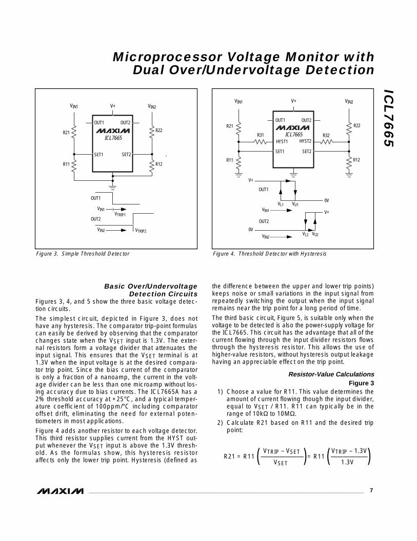
Basic Over/UndervoltageDetection Circuits
Figures 3, 4, and 5 show the three basic voltage detec-tion circuits.
The simplest circuit, depicted in Figure 3, does nothave any hysteresis. The comparator trip-point formulascan easily be derived by observing that the comparatorchanges state when the VSET input is 1.3V. The exter-nal resistors form a voltage divider that attenuates theinput signal. This ensures that the VSET terminal is at1.3V when the input voltage is at the desired compara-tor trip point. Since the bias current of the comparatoris only a fraction of a nanoamp, the current in the volt-age divider can be less than one microamp without los-ing accuracy due to bias currents. The ICL7665A has a2% threshold accuracy at +25°C, and a typical temper-ature coefficient of 100ppm/°C including comparatoroffset drift, eliminating the need for external poten-tiometers in most applications.
Figure 4 adds another resistor to each voltage detector.This third resistor supplies current from the HYST out-put whenever the VSET input is above the 1.3V thresh-old. As the formulas show, this hysteresis resistoraffects only the lower trip point. Hysteresis (defined as
the difference between the upper and lower trip points)keeps noise or small variations in the input signal fromrepeatedly switching the output when the input signalremains near the trip point for a long period of time.
The third basic circuit, Figure 5, is suitable only when thevoltage to be detected is also the power-supply voltage forthe ICL7665. This circuit has the advantage that all of thecurrent flowing through the input divider resistors flowsthrough the hysteresis resistor. This allows the use ofhigher-value resistors, without hysteresis output leakagehaving an appreciable effect on the trip point.
Resistor-Value CalculationsFigure 3
1) Choose a value for R11. This value determines theamount of current flowing though the input divider,equal to VSET / R11. R11 can typically be in therange of 10kΩ to 10MΩ.
2) Calculate R21 based on R11 and the desired trippoint:
VTRIP – VSET VTRIP – 1.3VR21 = R11 (———————)= R11 (——————)VSET 1.3V
ICL
76
65
Microprocessor Voltage Monitor withDual Over/Undervoltage Detection
_______________________________________________________________________________________ 7
Figure 3. Simple Threshold Detector Figure 4. Threshold Detector with Hysteresis
ICL7665
OUT1 OUT2
SET2SET1
R21
R11
R22
R12
VIN1 V+ VIN2
OUT1
VIN1VTRIP1
VTRIP2
OUT2
VIN2
ICL7665
OUT1 OUT2
SET2SET1
R21
R11
R22
R12
VIN1 V+ VIN2
HYST1 HYST2R31 R32
V+
OUT1
VL1 VU1
0V
V+
VU2
OUT2
VIN1
0V
VL2VIN2

ICL
76
65
Microprocessor Voltage Monitor withDual Over/Undervoltage Detection
8 _______________________________________________________________________________________
Figure 41) Choose a resistor value for R11. Typical values are
in the 10kΩ to 10MΩ range.2) Calculate R21 for the desired upper trip point, VU,
using the formula:
VU - VSET VU – 1.3VR21 = R11 (——————) = R11 (—————)VSET 1.3V
3) Calculate R31 for the desired amount of hysteresis:
(R21) (V+ – VSET) (R21) (V+ – 1.3V)R31 = ————————— = —————————
VU – VL VU – VL
or, if V+ = VIN:
(R21) (VL – VSET) (R21) (VL – 1.3V)R31 = ————————— = —————————
VU – VL VU – VL
4) The trip voltages are not affected by the absolutevalue of the resistors, as long as the impedancesare high enough that the resistance of R31 ismuch greater than the HYST output’s resistance,and the current through R31 is much higher thanthe HYST output’s leakage current. Normally, R31will be in the 100kΩ to 22MΩ range. Multiplying ordividing all three resistors by the same factor willnot affect the trip voltages.
Figure 51) Select a value for R11, usually between 10kΩ and
10MΩ.2) Calculate R21:
VL – VSET VL – 1.3VR21 = R11 (——————) = R11 (—————)VSET 1.3
3) Calculate R31:
VU – VLR31 = R11 (—————)VSET
4) As in the other circuits, all three resistor values maybe scaled up or down in value without changing VUand VL. VU and VL depend only on the ratio of thethree resistors, if the absolute values are such thatthe hysteresis output resistance and the leakagecurrents of the VSET input and hysteresis output canbe ignored.
__________Applications InformationFault Monitor for a Single Supply
Figure 6 shows a typical over/undervoltage fault monitorfor a single supply. In this case, the upper trip points (con-trolling OUT1) are centered on 5.5V, with 100mV of hys-teresis (VU = 5.55V, VL = 5.45V); and the lower trip points(controlling OUT2) are centered on 4.5V, also with 100mVof hysteresis. OUT1 and OUT2 are connected together ina wire-OR configuration to generate a power-OK signal.
Multiple-Supply Fault MonitorThe ICL7665 can simultaneously monitor several powersupplies, as shown in Figure 7. The easiest way to calculatethe resistor values is to note that when the VSET input is atthe trip point (1.3V), the current through R11 is 1.3V / R11.The sum of the currents through R21A, R21B and R31 mustequal this current when the two input voltages are at thedesired low-voltage detection point. Ordinarily, R21A andR21B are chosen so that the current through the two resis-tors is equal. Note that, since the voltage at the ICL7665VSET input depends on the voltage of both supplies beingmonitored, there will be some interaction between the low-voltage trip points for the two supplies. In this example,OUT1 will go low when either supply is 10% below nominal(assuming the other supply is at the nominal voltage), orwhen both supplies are 5% or more below their nominalvoltage. R31 sets the hysteresis, in this case, to about 43mVat the 5V supply or 170mV at the 15V supply. The secondsection of ICL7665 can be used to detect overvoltage or, asshown in Figure 7, can be used to detect the absence ofnegative supplies. Note that the trip points for OUT2 dependon both the voltages of the negative power supplies andthe actual voltage of the +5V supply.
Figure 5. Threshold Detector, VIN = V+
VL2 VU2
ICL7665
OUT1 OUT2
SET2SET1
R21
R11
VIN
HYST1 HYST2
OUT1
OUT2
VIN
V+
GND
OVERVOLTAGE UNDERVOLTAGE
R31 R32
R22
R12
VL1 VU1

ICL
76
65
Microprocessor Voltage Monitor withDual Over/Undervoltage Detection
_______________________________________________________________________________________ 9
Combination Low-Battery Warning andLow-Battery Disconnect
Nickel cadmium (NiCd) batteries are excellent recharge-able power sources for portable equipment, but caremust be taken to ensure that NiCd batteries are not damaged by overdischarge. Specifically, a NiCd batteryshould not be discharged to the point where the polarityof the lowest-capacity cell is reversed, and that cell isreverse charged by the higher-capacity cells. This reversecharging will dramatically reduce the life of a NiCd battery.The Figure 8 circuit both prevents reverse charging andgives a low-battery warning. A typical low-battery warningvoltage is 1V per cell. Since a NiCd “9V” battery is ordi-narily made up of six cells with a nominal voltage of 7.2V,a low-battery warning of 6V is appropriate, with a smallhysteresis of 100mV. To prevent overdischarge of a bat-tery, the load should be disconnected when the batteryvoltage is 1V x (N – 1), where N = number of cells. In thiscase, the low-battery load disconnect should occur at5V. Since the battery voltage will rise when the load isdisconnected, 800mV of hysteresis is used to preventrepeated on/off cycling.
Power-Fail Warning andPower-Up/Power-Down Reset
Figure 9 illustrates a power-fail warning circuit thatmonitors raw DC input voltage to the 7805 three-termi-nal 5V regulator. The power-fail warning signal goeshigh when the unregulated DC input falls below 8.0V.When the raw DC power source is disconnected or theAC power fails, the voltage on the input of the 7805decays at a rate of IOUT / C (in this case, 200mV/ms).Since the 7805 will continue to provide a 5V output at1A until VIN is less than 7.3V, this circuit will give atleast 3.5ms of warning before the 5V output begins todrop. If additional warning time is needed, either thetrip voltage or filter capacitance should be increased,or the output current should be decreased.
The ICL7665 OUT2 is set to trip when the 5V output hasdecayed to 3.9V. This output can be used to preventthe microprocessor from writing spurious data to aCMOS battery-backup memory, or can be used to acti-vate a battery-backup system.
AC Power-Fail and Brownout DetectorBy monitoring the secondary of the transformer, the cir-cuit in Figure 10 performs the same power-failure warn-ing function as Figure 9. With a normal 110V AC inputto the transformer, OUT1 will discharge C1 every16.7ms when the peak transformer secondary voltage
exceeds 10.2V. When the 110V AC power-line voltageis either interrupted or reduced so that the peak voltageis less than 10.2V, C1 will be charged through R1.OUT2, the power-fail warning output, goes high whenthe voltage on C1 reaches 1.3V. The time constant R1 xC1 determines the delay time before the power-fail warning signal is activated, in this case 42ms or 21⁄2 line cycles.Optional components R2, R3 and Q1 add hysteresis byincreasing the peak secondary voltage required to dis-charge C1 once the power-fail warning is active.
Battery Switchover CircuitThe circuit in Figure 11 performs two functions: switch-ing the power supply of a CMOS memory to a backupbattery when the line-powered supply is turned off, andlighting a low-battery-warning LED when the backupbattery is nearly discharged. The PNP transistor, Q1,connects the line-powered +5V to the CMOS memorywhenever the line-powered +5V supply voltage isgreater than 3.5V. The voltage drop across Q1 will onlybe a couple of hundred millivolts, since it will be satu-rated. Whenever the input voltage falls below 3.5V,OUT1 goes high, turns off Q1, and connects the 3Vlithium cell to the CMOS memory.
The second voltage detector of the ICL7665 monitors thevoltage of the lithium cell. If the battery voltage falls below2.6V, OUT2 goes low and the low-battery-warning LEDturns on (assuming that the +5V is present, of course).
Another possible use for the second section of theICL7665 is the detection of the input voltage fallingbelow 4.5V. This signal could then be used to preventthe microprocessor from writing spurious data to theCMOS memory while its power-supply voltage is out-side its guaranteed operating range.
Simple High/Low Temperature AlarmThe circuit in Figure 12 is a simple high/low tempera-ture alarm, which uses a low-cost NPN transistor as thesensor and an ICL7665 as the high/low detector. TheNPN transistor and potentiometer R1 form a Vbe multi-plier whose output voltage is determined by the Vbe ofthe transistor and the position of R1’s wiper arm. Thevoltage at the top of R1 will have a temperature coeffi-cient of approximately -5mV/°C. R1 is set so that thevoltage at VSET2 equals the VSET2 trip voltage when thetemperature of the NPN transistor reaches the levelselected for the high-temperature alarm. R2 can beadjusted so that the voltage at VSET1 is 1.3V when theNPN transistor’s temperature reaches the low-tempera-ture limit.

ICL
76
65
Microprocessor Voltage Monitor withDual Over/Undervoltage Detection
ICL7665
OUT2 OUT1
SET1SET2
HYST2
HYST1R3122M 22M
100k
POWER OK
301kR1149.9k
V+
+5V
-5V -15V
787k
+5V
+15V
R21A274k
R21B1.02M
+5V
HYST1
SET1
HYST2
SET2
GND OUT2
V+ V+ OUT1 OUT2
SHDN
SENSE
ICL7663ICL7665
GND
LOW-BATTERY WARNINGLOW-BATTERY SHUTDOWN
+5V, 1A OUTPUTR31
OUT1
SET
R21
R11
R32
R22
R12
1M 100Ω
Figure 8. Low-Battery Warning and Low-Battery Disconnect
Figure 7. Multiple-Supply Fault Monitor
HYST1
SET1
HYST2
SET2
ICL7665
V+
UNREGULATEDDC INPUT
BACK-UPBATTERY
RESETOR
WRITEENABLE
POWER-FAIL WARNING
4700µF 470µF
2.2M
1M
5.6M
715k
130k
22M
OUT2OUT1
5V, 1AOUTPUT7805
5V REGULATOR
HYST1
SET1
HYST2
SET2
OUT1 OUT2
ICL7665
V+
78055V REGULATOR10VAC
60Hz
20V CENTERTAPPED TRANS
4700µF
R21M
681k
Q1
R31M C1
R1
+5V
POWER-FAILWARNING
100k
5V, 1A
Figure 9. Power-Fail Warning and Power-Up/Power-Down Reset Figure 10. AC Power-Fail and Brownout Detector
ICL7665
OUT1 OUT2
SET2SET1
+5V SUPPLY
HYST1 HYST2V+
13M5%
7.5M5%
249k324k
100k 100kOVERVOLTAGE
DETECTORVU ≈ 5.55VVL ≈ 5.45V
UNDERVOLTAGEDETECTORVU ≈ 4.55VVL ≈ 4.45V
POWER OK
Figure 6. Fault Monitor for a Single Supply
10 ______________________________________________________________________________________

ICL
76
65
Microprocessor Voltage Monitor withDual Over/Undervoltage Detection
______________________________________________________________________________________ 11
HYST1
SET1
GND OUT2
SET2
HYST2
OUT1 V+
ICL7665
100k
2N43931M
LINE-POWERED+5V INPUT
Q1
1k
1µF
5.6M
1M
2.4M
220Ω
2N7000
22M
1M1%
1.15M1%
3VLITHIUMCELL
VCC TOCMOSMEMORY
Figure 11. Battery Switchover Circuit
Figure 12. Simple High/Low Temperature Alarm
HYST1
SET1
OUT2 OUT1
SET2
HYST2
V+
ICL7665R4
22M
R527k
R622M
R1, 1MHIGH-TEMPERATURELIMITADJUSTMENT
ALARMSIGNAL FOR
DRIVING LEDS,BELLS, ETC.
TEMPERATURESENSOR
(GENERALPURPOSE NPNTRANSISTOR)
R71.5M
R21M
LOW-TEMPERATURELIMIT ADJUST
9V
R3470k

_______________________SCR LatchupLike all junction-isolated CMOS circuits, the ICL7665 hasan inherent four-layer or SCR structure that can betriggered into destructive latchup under certain con-ditions. Avoid destructive latchup by following theseprecautions:
1) If either VSET terminal can be driven to a voltagegreater than V+ or less than ground, limit the inputcurrent to 500µA maximum. Usually, an input volt-age divider resistance can be chosen to ensurethe input current remains below 500µA, evenwhen the input voltage is applied before theICL7665 V+ supply is connected.
2) Limit the rate-of-rise of V+ by using a bypasscapacitor near the ICL7665. Rate-of-rise SCRsrarely occur unless: a) the battery has a lowimpedance—as is the case with NiCd and leadacid batteries; b) the battery is connected directlyto the ICL7665 or is switched on via a mechanicalswitch with low resistance; or c) there is little or noinput filter capacitance near the ICL7665. In line-powered systems, the rate-of-rise is usually limitedby other factors and will not cause a rate-of-riseSCR action under normal circumstances.
3) Limit the maximum supply voltage (including tran-sient spikes) to 18V. Likewise, limit the maximum volt-age on OUT1 and OUT2 to +18V and the maxi-mum voltage on HYST1 and HYST2 to 18V below V+.
ICL
76
65
Microprocessor Voltage Monitor withDual Over/Undervoltage Detection
PART TEMP. RANGE PIN-PACKAGEICL7665AC/D 0°C to +70°C Dice*
ICL7665EPA+ -40°C to +85°C 8 Plastic DIP
ICL7665AEPA+ -40°C to +85°C 8 Plastic DIP
ICL7665ESA+ -40°C to +85°C 8 SO
ICL7665AESA+ -40°C to +85°C 8 SO
___________________Chip Topography
_Ordering Information (continued)
ICL7665IPA+ -20°C to +85°C 8 Plastic DIP
ICL7665IJA+ -20°C to +85°C 8 CERDIP
*Contact factory for dice specifications.
OUT2
V+
HYST1
0.066"(1.42mm)
0.084"(1.63mm)
SET1 V-
SET2
HYST2
OUT1
TRANSISTOR COUNT: 38
SUBSTRATE CONNECTED TO V+.
Maxim cannot assume responsibility for use of any circuitry other than circuitry entirely embodied in a Maxim product. No circuit patent licenses areimplied. Maxim reserves the right to change the circuitry and specifications without notice at any time.
12 ____________________Maxim Integrated Products, 160 Rio Robles, San Jose, CA 95134 408-601-1000
© 2015 Maxim Integrated Products Printed USA is a registered trademark of Maxim Integrated Products.
+Denotes a lead(pb)-free/RoHS-compliant package.