Micromachining technologies for miniaturized … technologies for miniaturized communication devices...
15
Micromachining technologies for miniaturized communication devices Clark T.-C. Nguyen Center for Integrated Sensors and Circuits Department of Electrical Engineering and Computer Science University of Michigan Ann Arbor, Michigan 48109-2122 ABSTRACT An overview of the key micromachining technologies that enable communications applications for MEMS is presented with a focus on frequency-selective devices. In particular, micromechanical filters are briefly reviewed and key technologies needed to extend their frequencies into the high VHF and UHF ranges are anticipated. Series resistance in interconnect or structural materials is shown to be a common concern for virtually all RF MEMS components, from mechanical vibrating beams, to high-Q inductors and tunable capacitors, to switches and antennas. Environmental parasites—such as feedthrough capaci- tance, eddy currents, and molecular contaminants—are identified as major performance limiters for RF MEMS. Strategies for eliminating them via combinations of monolithic integration and encapsulation packaging are described. Keywords: RF, wireless, MEMS, micromechanical, resonator, filter, inductor, capacitor, switch, communications, Q 1. INTRODUCTION Due in large part to regulatory bodies, such as the Federal Communications Commission (FCC), virtually all major com- munication systems are based to some extent on partitioning of the electromagnetic frequency spectrum. This frequency mul- tiplexed nature of present day communication networks naturally demands that the enabling communication transceiver devices be capable of high frequency selectivity, i.e., capable of selecting a given frequency band while rejecting all others. Thus, frequency-selective devices—filters, oscillators, and mixers—constitute some of the most important components within a transceiver, and the availability and quality of these devices often dictate the overall architecture of a given transceiver. Unfortunately, advances in frequency-selective capabilities have lagged those for other transceiver functions, such as amplifiers or demodulation circuits, that directly benefited from the integrated circuit (IC) revolution. As a consequence, off- chip, highly selective, passive components are still used in the vast majority of today’s cordless and cellular phones, forcing board-level implementation of such devices and posing a significant bottleneck against the ultimate miniaturization of portable transceivers. The lack of suitable, miniature, frequency-selective devices has also influenced the architectural evolution of transceivers towards those that maximize the application range of transistor circuitry often at the expense of performance and power dissipation. For example, although dynamic range considerations force direct-conversion receivers to consume more power than their super-heterodyne counterparts, the former are still preferred over the latter because they have more relaxed frequency selection requirements, and thus, are more amenable to implementation via transistor integration. Fortunately, recent efforts to apply micromachining technologies to the miniaturization and integration of frequency- selective devices are starting to bring passive device technology on par with that of transistors. In particular, micromachining technologies have successfully achieved miniaturized and integrable versions of low loss, highly selective bandpass filters covering a wide range of frequencies (from 20 kHz to 90 GHz); high-Q inductors and tunable capacitors for voltage-controlled oscillators and matching networks; micromechanical low-loss switches for phased arrays and configurable power amplifiers; and ultra-high-Q resonators for stable reference oscillators. Figure 1 presents the typical block diagram for a super-heterodyne wireless transceiver, indicating the components that could greatly benefit from micromachined replacements. A more com- plete discussion of the specific micromachined devices applicable to communication transceivers is given in refs. 1 and 2. This paper reviews the specific micromachining technologies that have made the above devices possible. Discussion of technology begins in Section 3 with an account of the role that polysilicon surface micromachining has played in the imple- mentation of high-Q vibrating mechanical resonators and their associated applications. The resistive and Q deficiencies of pol- ysilicon are also discussed in this section, providing a convenient lead in for Sections 4 and 5, which consider alternative Additional author information: Full Address: 2406 EECS Bldg., 1301 Beal Ave, University of Michigan, Ann Arbor, MI 48109-2122 Tel: (734)764-1220, FAX: (734)763-9324, email: [email protected], http://www.eecs.umich.edu/~ctnguyen C. T.-C. Nguyen, “Micromachining technologies for miniaturized communication devices,” Proceedings of SPIE: Microma- chining and Microfabrication, Santa Clara, California, Sept. 20-22, 1998, pp. 24-38.
Transcript of Micromachining technologies for miniaturized … technologies for miniaturized communication devices...
Micromachining technologies for miniaturized communication devices
Clark T.-C. Nguyen
Center for Integrated Sensors and CircuitsDepartment of Electrical Engineering and Computer Science
University of MichiganAnn Arbor, Michigan 48109-2122
ABSTRACTAn overview of the key micromachining technologies that enable communications applications for MEMS is presented with afocus on frequency-selective devices. In particular, micromechanical filters are briefly reviewed and key technologies neededto extend their frequencies into the high VHF and UHF ranges are anticipated. Series resistance in interconnect or structuralmaterials is shown to be a common concern for virtually all RF MEMS components, from mechanical vibrating beams, tohigh-Q inductors and tunable capacitors, to switches and antennas. Environmental parasites—such as feedthrough capaci-tance, eddy currents, and molecular contaminants—are identified as major performance limiters for RF MEMS. Strategies foreliminating them via combinations of monolithic integration and encapsulation packaging are described.
Keywords: RF, wireless, MEMS, micromechanical, resonator, filter, inductor, capacitor, switch, communications, Q
1. INTRODUCTIONDue in large part to regulatory bodies, such as the Federal Communications Commission (FCC), virtually all major com-
munication systems are based to some extent on partitioning of the electromagnetic frequency spectrum. This frequency mul-tiplexed nature of present day communication networks naturally demands that the enabling communication transceiverdevices be capable of high frequency selectivity, i.e., capable of selecting a given frequency band while rejecting all others.Thus, frequency-selective devices—filters, oscillators, and mixers—constitute some of the most important components withina transceiver, and the availability and quality of these devices often dictate the overall architecture of a given transceiver.
Unfortunately, advances in frequency-selective capabilities have lagged those for other transceiver functions, such asamplifiers or demodulation circuits, that directly benefited from the integrated circuit (IC) revolution. As a consequence, off-chip, highly selective, passive components are still used in the vast majority of today’s cordless and cellular phones, forcingboard-level implementation of such devices and posing a significant bottleneck against the ultimate miniaturization of portabletransceivers. The lack of suitable, miniature, frequency-selective devices has also influenced the architectural evolution oftransceivers towards those that maximize the application range of transistor circuitry often at the expense of performance andpower dissipation. For example, although dynamic range considerations force direct-conversion receivers to consume morepower than their super-heterodyne counterparts, the former are still preferred over the latter because they have more relaxedfrequency selection requirements, and thus, are more amenable to implementation via transistor integration.
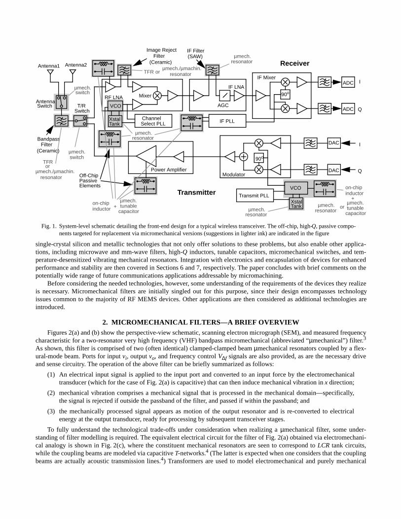
Fortunately, recent efforts to apply micromachining technologies to the miniaturization and integration of frequency-selective devices are starting to bring passive device technology on par with that of transistors. In particular, micromachiningtechnologies have successfully achieved miniaturized and integrable versions of low loss, highly selective bandpass filterscovering a wide range of frequencies (from 20 kHz to 90 GHz); high-Q inductors and tunable capacitors for voltage-controlledoscillators and matching networks; micromechanical low-loss switches for phased arrays and configurable power amplifiers;and ultra-high-Q resonators for stable reference oscillators. Figure 1 presents the typical block diagram for a super-heterodynewireless transceiver, indicating the components that could greatly benefit from micromachined replacements. A more com-plete discussion of the specific micromachined devices applicable to communication transceivers is given in refs. 1 and 2.
This paper reviews the specific micromachining technologies that have made the above devices possible. Discussion oftechnology begins in Section 3 with an account of the role that polysilicon surface micromachining has played in the imple-mentation of high-Q vibrating mechanical resonators and their associated applications. The resistive and Q deficiencies of pol-ysilicon are also discussed in this section, providing a convenient lead in for Sections 4 and 5, which consider alternative
Additional author information:Full Address: 2406 EECS Bldg., 1301 Beal Ave, University of Michigan, Ann Arbor, MI 48109-2122Tel: (734)764-1220, FAX: (734)763-9324, email: [email protected], http://www.eecs.umich.edu/~ctnguyen
C. T.-C. Nguyen, “Micromachining technologies for miniaturized communication devices,” Proceedings of SPIE: Microma-chining and Microfabrication, Santa Clara, California, Sept. 20-22, 1998, pp. 24-38.
single-crystal silicon and metallic technologies that not only offer solutions to these problems, but also enable other applica-tions, including microwave and mm-wave filters, high-Q inductors, tunable capacitors, micromechanical switches, and tem-perature-desensitized vibrating mechanical resonators. Integration with electronics and encapsulation of devices for enhancedperformance and stability are then covered in Sections 6 and 7, respectively. The paper concludes with brief comments on thepotentially wide range of future communications applications addressable by micromachining.
Before considering the needed technologies, however, some understanding of the requirements of the devices they realizeis necessary. Micromechanical filters are initially singled out for this purpose, since their design encompasses technologyissues common to the majority of RF MEMS devices. Other applications are then considered as additional technologies areintroduced.
2. MICROMECHANICAL FILTERS—A BRIEF OVERVIEWFigures 2(a) and (b) show the perspective-view schematic, scanning electron micrograph (SEM), and measured frequency
characteristic for a two-resonator very high frequency (VHF) bandpass micromechanical (abbreviated “µmechanical”) filter.3
As shown, this filter is comprised of two (often identical) clamped-clamped beam µmechanical resonators coupled by a flex-ural-mode beam. Ports for input vi, output vo, and frequency control V∆f signals are also provided, as are the necessary driveand sense circuitry. The operation of the above filter can be briefly summarized as follows:
(1) An electrical input signal is applied to the input port and converted to an input force by the electromechanicaltransducer (which for the case of Fig. 2(a) is capacitive) that can then induce mechanical vibration in x direction;
(2) mechanical vibration comprises a mechanical signal that is processed in the mechanical domain—specifically,the signal is rejected if outside the passband of the filter, and passed if within the passband; and
(3) the mechanically processed signal appears as motion of the output resonator and is re-converted to electricalenergy at the output transducer, ready for processing by subsequent transceiver stages.
To fully understand the technological trade-offs under consideration when realizing a µmechanical filter, some under-standing of filter modelling is required. The equivalent electrical circuit for the filter of Fig. 2(a) obtained via electromechani-cal analogy is shown in Fig. 2(c), where the constituent mechanical resonators are seen to correspond to LCR tank circuits,while the coupling beams are modeled via capacitive T-networks.4 (The latter is expected when one considers that the couplingbeams are actually acoustic transmission lines.4) Transformers are used to model electromechanical and purely mechanical
Fig. 1. System-level schematic detailing the front-end design for a typical wireless transceiver. The off-chip, high-Q, passive compo-nents targeted for replacement via micromechanical versions (suggestions in lighter ink) are indicated in the figure
Antenna1
XstalTank
90o
ADC
ADC
90o
XstalTank
Antenna2
BandpassFilter
IF Mixer
Power Amplifier
IF PLL
Image RejectFilter
Transmit PLL
Modulator
ChannelSelect PLL
DAC
RF LNA
IF LNA
AGC
I
Q
AntennaSwitch
SwitchT/R
(Ceramic)
(Ceramic)
Mixer
VCO
DAC
Q
I
Receiver
Transmitter
Off-ChipPassiveElements
TFRor
µmech.
on-chipinductor
resonator
µmech.tunable
capacitor
µmech.switch
µmech./µmachin.resonator
+
µmech.switch
on-chipinductor
µmech.tunable
capacitor
+
TFR orµmech./µmachin.
resonator
orµmech.resonator
µmech.resonator
µmech.resonator
IF Filter(SAW)
VCO
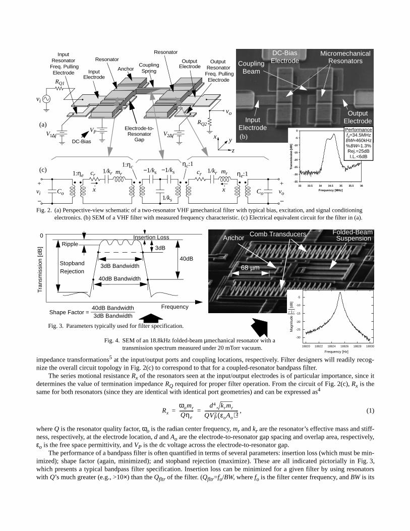
impedance transformations5 at the input/output ports and coupling locations, respectively. Filter designers will readily recog-nize the overall circuit topology in Fig. 2(c) to correspond to that for a coupled-resonator bandpass filter.
The series motional resistance Rx of the resonators seen at the input/output electrodes is of particular importance, since itdetermines the value of termination impedance RQ required for proper filter operation. From the circuit of Fig. 2(c), Rx is thesame for both resonators (since they are identical with identical port geometries) and can be expressed as4
, (1)
where Q is the resonator quality factor, ωo is the radian center frequency, mr and kr are the resonator’s effective mass and stiff-ness, respectively, at the electrode location, d and Ao are the electrode-to-resonator gap spacing and overlap area, respectively,εo is the free space permittivity, and VP is the dc voltage across the electrode-to-resonator gap.
The performance of a bandpass filter is often quantified in terms of several parameters: insertion loss (which must be min-imized); shape factor (again, minimized); and stopband rejection (maximize). These are all indicated pictorially in Fig. 3,which presents a typical bandpass filter specification. Insertion loss can be minimized for a given filter by using resonatorswith Q’s much greater (e.g., >10×) than the Qfltr of the filter. (Qfltr=fo/BW, where fo is the filter center frequency, and BW is its
Fig. 2. (a) Perspective-view schematic of a two-resonator VHF µmechanical filter with typical bias, excitation, and signal conditioning electronics. (b) SEM of a VHF filter with measured frequency characteristic. (c) Electrical equivalent circuit for the filter in (a).
V1∆f
Anchor SpringCoupling
OutputElectrode
InputElectrode
Input
Freq. PullingElectrode
Resonator Output
Freq. PullingElectrode
Resonator
RQ2
vo
RQ1
vi
VP V2∆f
ResonatorResonator
Electrode-to-Resonator
GapDC-Bias
cr mr
1/ks
1/kr−1/ks−1/ks
1:ηc ηc:1
Covi
+
−
cr mr1/kr
Co vo
+
−
1:ηe ηe:1
x·x·
MicromechanicalResonatorsCoupling
Beam
-35
-30
-25
-20
-15
-10
-5
0
33 33.5 34 34.5 35 35.5 36
Frequency [MHz]
Tra
nsm
issi
on
[dB
]
Performancefo=34.5MHzBW=460kHz%BW=1.3%Rej.=25dBI.L.<6dB
(a)
(b)
(c)
InputElectrode
OutputElectrode
DC-BiasElectrode
x y
z
Rx
ωomr
Qηe-------------
d4 krmr
QVP2 εoAo( )2
------------------------------= =
Fig. 3. Parameters typically used for filter specification.
Ripple3dB
40dBStopbandRejection
40dB Bandwidth
Tran
smis
sion
[dB
]
0
Frequency
Insertion Loss
3dB Bandwidth
Shape Factor = 40dB Bandwidth3dB Bandwidth
Fig. 4. SEM of an 18.8kHz folded-beam µmechanical resonator with a transmission spectrum measured under 20 mTorr vacuum.
Anchor Comb Transducers Folded-BeamSuspension
68 µm
-30
-25
-20
-15
-10
-5
18820 18822 18824 18826 18828 18830
Frequency [Hz]
Mag
nitu
de
[
dB]
v o v i

bandwidth.) Shape factor improves as the number of resonators in a given filter increases. However, unless the Q of the con-stituent resonators is sufficiently high, the number of resonators can be increased only at the expense of increased insertionloss. Thus, high resonator Q is also required for small shape factor. Finally, stopband rejection is dictated by not only shapefactor, but also by the amount of parasitic feedthrough coupling the filter input to its output, which in turn is strongly depen-dent on the technology (e.g., whether sufficient grounding is available, or whether a shielding cap is available).
Another key design parameter that often is not a major consideration for off-chip filters, but that is of utmost importancefor µmechanical filters, is termination impedance RQ. In particular, a filter is normally designed to function correctly (i.e., withthe desired passband shape) only when a specific value of impedance loads its input and output ports. For many systems, ter-mination impedances around 50 or 75Ω (dictated by the antenna) are often required at RF, while larger values approaching 1-3kΩ are acceptable at IF frequencies. These impedances can be achieved by micro-scale filters only if sufficient electrome-chanical coupling is provided via the filter input and output transducers. The expression governing the termination resistancerequired for the filter of Fig. 2 depends upon Rx and can be expressed as4
, (2)
where Qfltr is the filter quality factor, qi is a normalized coefficient obtained from a filter cookbook,6 and where the most prac-tical controllable parameters have been singled out in the final expression to the far right. As dictated by (2), RQ is stronglydependent on the dc-bias VP applied across the port in question and on the electrode-to-resonator gap spacing d. In many oftoday’s portable wireless applications, the supply voltage is greatly limited, so increasing VP may not be an option. Overlaparea Ao may also be constrained by resonator geometry. The gap spacing d, on the other hand, is limited mainly by technology.To achieve termination impedance values on the order of 50Ω for VHF to UHF filters, gap spacings of less than 500Å arerequired (the exact value depending heavily on %BW and VP). For termination resistances greater than 1kΩ, gap spacingsgreater than 1000Å can be utilized.
3. POLYSILICON SURFACE MICROMACHININGPolycrystalline silicon has so far been the material of choice for HF and VHF vibrating µmechanical resonators intended
for bandpass filters and stable reference oscillators. The reason is that polysilicon offers an excellent compromise betweenhigh material Q and maximum design flexibility. In particular, the Q of polysilicon µmechanical resonators under vacuum hasbeen measured in excess of 50,000 at MF frequencies (Fig. 4)7 and on the order of 10,000 at VHF frequencies (Fig. 5). (Notethat vacuum is necessary to attain these Q’s, since at atmospheric pressure these micro-scale resonators must expend a signifi-cant fraction of their total energy per cycle to push air molecules aside.8) In addition, geometric design flexibility is especiallyimportant when implementing complex filters, such as the MF three-resonator version shown in Fig. 6, which features numer-ous additional ports for feedthrough suppression and post-fabrication tuning.9 For devices as complex as this one, polysiliconsurface micromachining—in which critical features are defined in a single masking step (no alignment necessary) and anchorscan be placed virtually anywhere on the substrate surface—constitutes one of the best technological choices.
The fundamental procedure behind polysilicon surface micromachining10 is summarized succinctly in Fig. 7. In this pro-cedure, a sequence of IC-compatible film depositions and patternings are used to achieve a structure with the cross sectionshown in Fig. 7(a). Here, after definition of isolation dielectrics and polysilicon interconnect, a (sacrificial) oxide layer is tem-porarily used to support the structural polysilicon layer during deposition, doping, and patterning. After achieving the structureof Fig. 7(a), the whole structure is immersed in a solution of hydrofluoric acid (HF), which attacks the sacrificial oxide layer,but leaves the polysilicon layer relatively intact. The result: A free standing polysilicon beam, free to move in any directionupon application of an electrostatic force. It should be mentioned that Fig. 7 omits many important details that must be consid-ered in actual fabrication runs. In particular, the intrinsic Q of resulting resonators has been found to be heavily dependentupon several process details, including the method used to dope the polysilicon material.4 Post-process steps, such as localizedannealing, can also greatly influence resonator Q and stability.11
Figure 7 actually illustrates a very conventional polysilicon surface micromachining process, used frequently for commer-cial products12 and used for the MF filter of Fig. 6 (and for the MF oscillator of Fig. 25(b)). This process is fairly conservativein that 2 µm sacrificial oxide spacers are utilized. Thus, high frequency capacitively-transduced filters using resonators mov-ing perpendicular to the substrate cannot use this process for reasons discussed in the previous section: gaps on the order offrom 200Å to 1000Å are required between electrodes and polysilicon structures. Lithographically, submicron lateral gaps forresonance parallel to the substrate are possible via e-beam lithography combined with aggressive etch technologies (discussedlater), but this approach still requires extensive research. Thus, although many MF resonators have benefited from the flexibil-ity of lateral vibration (Fig. 6), lithographic limitations have so far prevented practical VHF µmechanical resonators and their
RQ RxQ
qiQfltr
--------------- 1– d4
VP2 Ao
2-------------∝=
associated filters from vibrating parallel to the substrate. Rather, these devices vibrate perpendicular to the substrate, with elec-trode-to-resonator gaps defined by sacrificial oxide thicknesses, which can easily be made down to 200Å or less. In particular,the 54.2 MHz polysilicon µmechanical resonator of Fig. 5 features a 300Å electrode-to-resonator gap.
Unfortunately, the use of such a small vertical gap in polysilicon surface micromachining comes riddled with several pro-cessing details/hindrances. Many of these arise from the now very thin sacrificial oxide layers used to define these gaps, andcan be enumerated as follows:
(1) Sacrificial layer uniformity is now an issue, and precautions must be taken to prevent pinholes.
(2) In previous large-spacer surface micromachining processes, the sacrificial oxide protected underlying intercon-nect polysilicon layers during the overetch step in structural polysilicon patterning. For the case of thin gaps,however, the sacrificial oxide may no longer be thick enough to protect underlying layers when conventional RIEetchers are used. Rather, high density plasma etchers with much higher silicon-to-oxide etch selectivities maynow be required.
(3) Due to reactant diffusion limitations, the sacrificial etch takes much longer with thin gaps than for previouslarge-gapped processes. This is problematic, because although HF attacks polysilicon much more slowly than
Fig. 5. SEM of a 54.2 MHz folded-beam microme-chanical resonator with a transmission spectrum measured under 20 mTorr vacuum.
Fig. 6. Full-view (a) and zoom-in (b) SEM’s of a three-resonator, MF, micromechanical filter with measured transmission spectrum.5 This filter features ratioed folded-beam, comb-driven resonators that vibrate parallel to the substrate.
Fig. 7. Cross-sections depicting the fabrication sequence used in poly-silicon surface micromachining. (a) Required film layers up to the release etch step. (b) Resulting free-standing beam follow-ing a release etch in hydrofluoric acid.
Fig. 8. Overhead-view photograph showing compro-mised polysilicon, but intact chrome/gold metal, in the electrodes after a 30 minute sac-rificial release step in hydrofluoric acid.
-75
-70
-65
-60
-55
-50
-45
-40
-35
53.8 54 54.2 54.4 54.6 54.8
Frequency [MHz]
Tran
smis
sio
n [
dB
]
Qmeas=840 (with RP)
54.2MHz
Qextract=9,000
Metallization
AnchorPolysilicon
Interconnect
PolysiliconResonator
Beam
Drive ElectrodeBias/Sense Electrode Ratioed Folded-Beam
Coupling Beam
Folding Truss
Anchor
Comb-Transducer
Lsij=95µm
20µm
32µm
Drive Resonator Sense Resonator
Tran
smis
sion
[dB
]
Frequency [kHz]
-60
-50-40
-30-20
-100
337 338 339 340 341 342 343
fo=340kHzBW=403Hz
%BW=0.09%Stop.R.=64 dB
I.L.<0.6 dB
Interconnect PolysiliconRemoved
Interconnect PolysiliconAttacked (Roughened)
Oxide
2 um
2 um
Polycrystalline Silicon(600-650 C)o
Sacrifical Oxide (450 C)o
SiliconNitride(835 C)o
Oxide
Silicon Substrate
Silicon Substrate
Free standingPolycrstalline Silicon Beam
2 um
Hydroflouric Acid
(a)
(b)
MetalIntact
oxide, it still attacks at a finite rate. Attack of polysilicon interconnect by HF has been observed, as has evidenceof dopant extraction from polysilicon by HF during long release etches, both of which greatly increase the seriesresistance of resonator input and output electrodes.
The increase in series resistance described in item (3) is quite detrimental to resonator performance, and is largely respon-sible for the low value of measured Q shown in Fig. 5. For cases where polysilicon alone (i.e., no metallization) is used asinterconnect, the phenomena in item (3) can lead to electrode RS’s (both input and dc-bias electrodes) on the order of from 2-10kΩ for the resonator of Fig. 5, depending upon the needed release etch time. With metallization, where all polysilicon inter-connect is covered by metal except for those portions within 15 µm of the resonator, RS can be reduced to 0.15-2kΩ. For theparticular resonator of Fig. 5, the total on-chip interconnect resistance amounted to ~180Ω, which, considering a calculatedvalue for Rx=28Ω for this resonator (under the measurement conditions used for Fig. 5), can still seriously load the Q of theresonator. Thus, the measured Q in the spectrum of Fig. 5 actually represents the loaded Q (Qloaded), not the actual resonatorQ. The loaded Q is given by the expression
, (3)
which stresses the importance of minimizing RS relative to Rx. Rearranging (3), the actual unloaded Q of the resonator is foundto be about 9,000. Thus, the Q of this resonator has been severely degraded from 9,000 to 840 by the excessive parasitic seriesresistance. To illustrate the severity of such Q-degradation: A 70 MHz, 0.3% bandwidth, three-resonator filter implementedusing resonators with Q’s of 9,000 would show an insertion loss of ~1.5dB—very good. In contrast, if resonators with Q’s of840 were used, the insertion loss would be ~20dB, which is unacceptable for most applications.
The Q of the resonator of Fig.5 could be maximized if the electrodes were comprised entirely of metal. Unfortunately,many fabrication sites (including ours) cannot do this, due to a need to keep metal contamination away from polysilicon andoxide LPCVD tubes used for circuits processes, as well as micromechanics. Thus, the metal/poly composite interconnect ofFig. 5 was merely a good compromise. At first glance, metallization seems straightforward via a simple lift-off technique.However, the long HF release etch required for small gaps, combined with electrolytic reactions, greatly complicate the metal-lization process. In particular, the type of metal used must be carefully selected to insure a sufficiently low rate of attack byHF. Although aluminum etches very slowly in 48.8 wt. % concentrated HF, the etch rate is not slow enough to withstand a verylong, small-gapped, release etch. Chrome/gold metallization is a better choice for HF release etches. Unfortunately, however,chrome/gold in contact with polysilicon in an HF solution gives rise to an electrolytically enhanced reaction that dissolvesaway the polysilicon layer. The end result is shown in Fig. 8, where obvious removal of polysilicon interconnect is seen, whilethe metal remains intact. The resulting polysilicon shows RS’s as high as 50kΩ—quite unacceptable for high Q applications.
The solution to the above problem is to metallize after the release etch. For this to be practical, the released structuresmust be able to withstand a photoresist spin cycle. This is not a problem for high frequency µmechanical resonators, whichhave stiffnesses on the order of 2,000 to 100,000 N/m, but can be a problem for very compliant structures, such as those usedfor accelerometers, which have stiffnesses on the order of 1 N/m or less. Also worth mentioning for post release metallizationis the need to keep the metal defining photoresist on the wafer during dicing, so that the dicing slurry does not interfere withthe resonators, e.g., by seeping into gaps and/or contaminating the resonator surfaces.
Although metallization helps to greatly reduce interconnect series resistance, it may not be enough in many cases, sincethe metal cannot cover the polysilicon interconnect near the resonator. If buying extra LPCVD tubes that allow metal elec-trodes is not an option, other strategies that reduce the resistance in polysilicon interconnect are needed.
One strategy presently under investigation attempts to return to lateral resonator operation, as illustrated in Fig. 9, wherevibrations parallel to the substrate are now excited by lateral gap capacitive transducers. Here, much thicker electrodes can beused, resulting in much smaller polysilicon electrode RS’s, on the order of 1-2Ω. Also, the dopant loss and interconnect attackproblems described above are no longer factors. The cross-section of Fig. 9 can be achieved in a surface-micromachining pro-cess using e-beam lithography and high density plasma etching to define resonator and electrode features. Fig. 10 shows worktowards the structure of Fig. 9, in which an inductively coupled (ICP) high density plasma source is used with a nickel mask todry etch 0.1 µm gaps in 3.1 µm-thick silicon using a Cl2 chemistry.13 Although promising, this technique presently cannotmatch the d’s and Ao’s of vertical resonator processes. In particular, as dictated by (3), until sub-500Å gaps can be achieved inpolysilicon films thicker than 5 µm, lateral resonator technologies such as this will struggle to achieve filters with terminationresistance values less than 100Ω. In the meantime, other technologies have recently arisen that may allow thin lateral gapsbetween much thicker silicon layers. One very recent technology uses conformal carbonated parylene to achieve vertical sacri-ficial layers for more accurate molding in hexsil processes.14 Sacrificial layer removal is done using an oxygen plasma, which
Qloaded QRx
Rx RS+------------------
=
prevents attack of structural layers. This technology has goodpotential for application to surface-micromachining.
Thus far, this discussion has centered on polysilicon µme-chanical resonators utilizing capacitive transduction. Thisemphasis reflects the fact that virtually all successful µme-chanical filters (using two resonators or more) to date have uti-lized capacitive transduction. This statement in turn reflectsthe advantages of capacitive transduction, which include process simplicity and less susceptibility to bimorph-derived temper-ature dependencies. Nevertheless, capacitive transduction does have its drawbacks. In particular, its electromechanical cou-pling coefficient depends inversely on the electrode-to-resonator overlap area Ao. Thus, with capacitive transduction,increasing resonator frequency to satisfy higher communication bands is no longer just a matter of reducing resonator geome-tries; rather, alternative designs that attain higher frequencies without excessive reductions in Ao must be used. On the otherhand, such alternative resonator designs may be avoidable via alternative transduction techniques, such as piezoelectric15 andmagnetomotive.16 These methods, however, also have drawbacks. In particular, piezoelectric materials are difficult to deposituniformly, and piezoelectric transduction often entails the use of bilayer structures with potentially increased temperature sen-sitivity. For the case of magnetomotive transduction, the permeabilities of the magnets used have limited bandwidths and arethus not effective at UHF frequencies. The search for optimum transduction methods continues.
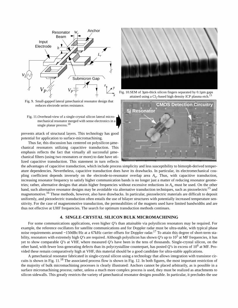
4. SINGLE-CRYSTAL SILICON BULK MICROMACHININGFor some communications applications, even higher Q’s than attainable via polysilicon resonators may be required. For
example, the reference oscillators for satellite communications and for Doppler radar must be ultra-stable, with typical phasenoise requirements around −150dBc/Hz at a 67kHz carrier offsets for Doppler radar.17 To attain this degree of short-term sta-bility, resonators with extremely high Q’s are required. Although polysilicon has shown Q’s up to 105 at MF frequencies, it hasyet to show comparable Q’s at VHF, where measured Q’s have been in the tens of thousands. Single-crystal silicon, on theother hand, with fewer loss-generating defects than its polycrystalline counterpart, has posted Q’s in excess of 106 at MF. Pro-vided these remain comparatively high at VHF, this material should be a good candidate for ultra-stable applications.
A µmechanical resonator fabricated in single-crystal silicon using a technology that allows integration with transistor cir-cuits is shown in Fig. 11.18 The associated process flow is shown in Fig. 12. In both figures, the most important restriction ofthe majority of bulk micromachining processes is clearly illustrated: Anchors cannot be placed arbitrarily, as is possible in asurface micromachining process; rather, unless a much more complex process is used, they must be realized as attachments tosilicon sidewalls. This greatly restricts the variety of µmechanical resonator designs possible. In particular, it precludes the use
Fig. 9. Small-gapped lateral µmechanical resonator design that reduces electrode series resistance.
Fig. 10.SEM of 3µm-thick silicon fingers separated by 0.1µm gaps attained using a Cl2-based high density ICP plasma etch.13
Fig. 11.Overhead-view of a single-crystal silicon lateral micro-mechanical resonator merged with sense electronics in a single planar process.18
ResonatorBeam
vi
VP
InputElectrode
Submicron Gap
Anchor
x
yz
Wr
VP
Lr
h
Si ResonatorCMOS Detection Circuitry
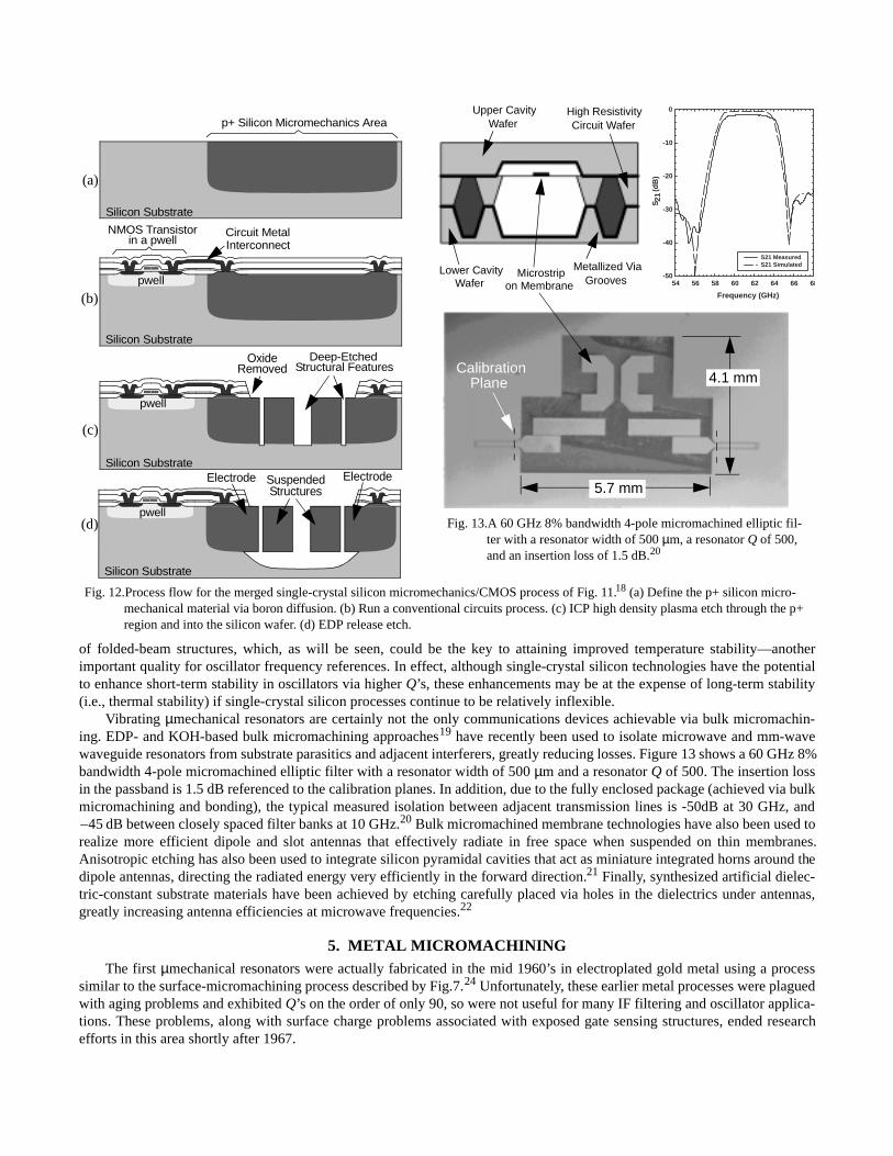
of folded-beam structures, which, as will be seen, could be the key to attaining improved temperature stability—anotherimportant quality for oscillator frequency references. In effect, although single-crystal silicon technologies have the potentialto enhance short-term stability in oscillators via higher Q’s, these enhancements may be at the expense of long-term stability(i.e., thermal stability) if single-crystal silicon processes continue to be relatively inflexible.
Vibrating µmechanical resonators are certainly not the only communications devices achievable via bulk micromachin-ing. EDP- and KOH-based bulk micromachining approaches19 have recently been used to isolate microwave and mm-wavewaveguide resonators from substrate parasitics and adjacent interferers, greatly reducing losses. Figure 13 shows a 60 GHz 8%bandwidth 4-pole micromachined elliptic filter with a resonator width of 500 µm and a resonator Q of 500. The insertion lossin the passband is 1.5 dB referenced to the calibration planes. In addition, due to the fully enclosed package (achieved via bulkmicromachining and bonding), the typical measured isolation between adjacent transmission lines is -50dB at 30 GHz, and
dB between closely spaced filter banks at 10 GHz.20 Bulk micromachined membrane technologies have also been used torealize more efficient dipole and slot antennas that effectively radiate in free space when suspended on thin membranes.Anisotropic etching has also been used to integrate silicon pyramidal cavities that act as miniature integrated horns around thedipole antennas, directing the radiated energy very efficiently in the forward direction.21 Finally, synthesized artificial dielec-tric-constant substrate materials have been achieved by etching carefully placed via holes in the dielectrics under antennas,greatly increasing antenna efficiencies at microwave frequencies.22
5. METAL MICROMACHININGThe first µmechanical resonators were actually fabricated in the mid 1960’s in electroplated gold metal using a process
similar to the surface-micromachining process described by Fig.7.24 Unfortunately, these earlier metal processes were plaguedwith aging problems and exhibited Q’s on the order of only 90, so were not useful for many IF filtering and oscillator applica-tions. These problems, along with surface charge problems associated with exposed gate sensing structures, ended researchefforts in this area shortly after 1967.
Fig. 12.Process flow for the merged single-crystal silicon micromechanics/CMOS process of Fig. 11.18 (a) Define the p+ silicon micro-mechanical material via boron diffusion. (b) Run a conventional circuits process. (c) ICP high density plasma etch through the p+ region and into the silicon wafer. (d) EDP release etch.
Fig. 13.A 60 GHz 8% bandwidth 4-pole micromachined elliptic fil-ter with a resonator width of 500 µm, a resonator Q of 500, and an insertion loss of 1.5 dB.20
Frequency (GHz)
54 56 58 60 62 64 66 68
S 21
(dB
)
-50
-40
-30
-20
-10
0
S21 MeasuredS21 Simulated
5.7 mm
4.1 mmCalibration
Plane
Upper Cavity
Lower Cavity Microstripon Membrane
Wafer
Wafer
Metallized ViaGrooves
High ResistivityCircuit Wafer
Silicon Substrate
p+ Silicon Micromechanics Area
Circuit MetalInterconnect
pwell
Silicon Substrate
NMOS Transistorin a pwell
pwell
Silicon Substrate
Deep-EtchedStructural Features
OxideRemoved
pwell
Silicon Substrate
(a)
(b)
(c)
(d)
SuspendedStructures
ElectrodeElectrode
45–
Although not a first choice for vibrating resonator applications, metal technologies have certainly been important for othercommunications applications. In particular, the Q of integrated inductors and tunable capacitors, and the insertion loss of µme-chanical switches, are all heavily dependent upon the series resistance of their construction materials. Thus, metals have beena natural material choice for these applications.
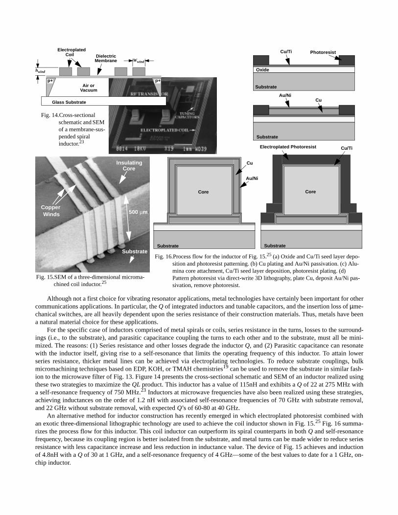
For the specific case of inductors comprised of metal spirals or coils, series resistance in the turns, losses to the surround-ings (i.e., to the substrate), and parasitic capacitance coupling the turns to each other and to the substrate, must all be mini-mized. The reasons: (1) Series resistance and other losses degrade the inductor Q, and (2) Parasitic capacitance can resonatewith the inductor itself, giving rise to a self-resonance that limits the operating frequency of this inductor. To attain lowerseries resistance, thicker metal lines can be achieved via electroplating technologies. To reduce substrate couplings, bulkmicromachining techniques based on EDP, KOH, or TMAH chemistries19 can be used to remove the substrate in similar fash-ion to the microwave filter of Fig. 13. Figure 14 presents the cross-sectional schematic and SEM of an inductor realized usingthese two strategies to maximize the QL product. This inductor has a value of 115nH and exhibits a Q of 22 at 275 MHz witha self-resonance frequency of 750 MHz.23 Inductors at microwave frequencies have also been realized using these strategies,achieving inductances on the order of 1.2 nH with associated self-resonance frequencies of 70 GHz with substrate removal,and 22 GHz without substrate removal, with expected Q’s of 60-80 at 40 GHz.
An alternative method for inductor construction has recently emerged in which electroplated photoresist combined withan exotic three-dimensional lithographic technology are used to achieve the coil inductor shown in Fig. 15.25 Fig. 16 summa-rizes the process flow for this inductor. This coil inductor can outperform its spiral counterparts in both Q and self-resonancefrequency, because its coupling region is better isolated from the substrate, and metal turns can be made wider to reduce seriesresistance with less capacitance increase and less reduction in inductance value. The device of Fig. 15 achieves and inductionof 4.8nH with a Q of 30 at 1 GHz, and a self-resonance frequency of 4 GHz—some of the best values to date for a 1 GHz, on-chip inductor.
Substrate
Oxide
Substrate
Substrate
Core
Substrate
Core
Fig. 14.Cross-sectional schematic and SEM of a membrane-sus-pended spiral inductor.23
Fig. 15.SEM of a three-dimensional microma-chined coil inductor.25
Fig. 16.Process flow for the inductor of Fig. 15.25 (a) Oxide and Cu/Ti seed layer depo-sition and photoresist patterning. (b) Cu plating and Au/Ni passivation. (c) Alu-mina core attachment, Cu/Ti seed layer deposition, photoresist plating. (d) Pattern photoresist via direct-write 3D lithography, plate Cu, deposit Au/Ni pas-sivation, remove photoresist.
DielectricMembrane
ElectroplatedCoil
p+
Glass Substrate
Air orVacuum
hwind
InsulatingCore
CopperWinds
Substrate
500 µm
Cu/Ti Photoresist
CuAu/Ni
Electroplated Photoresist Cu/Ti
Cu
Au/Ni
Wwind
p+
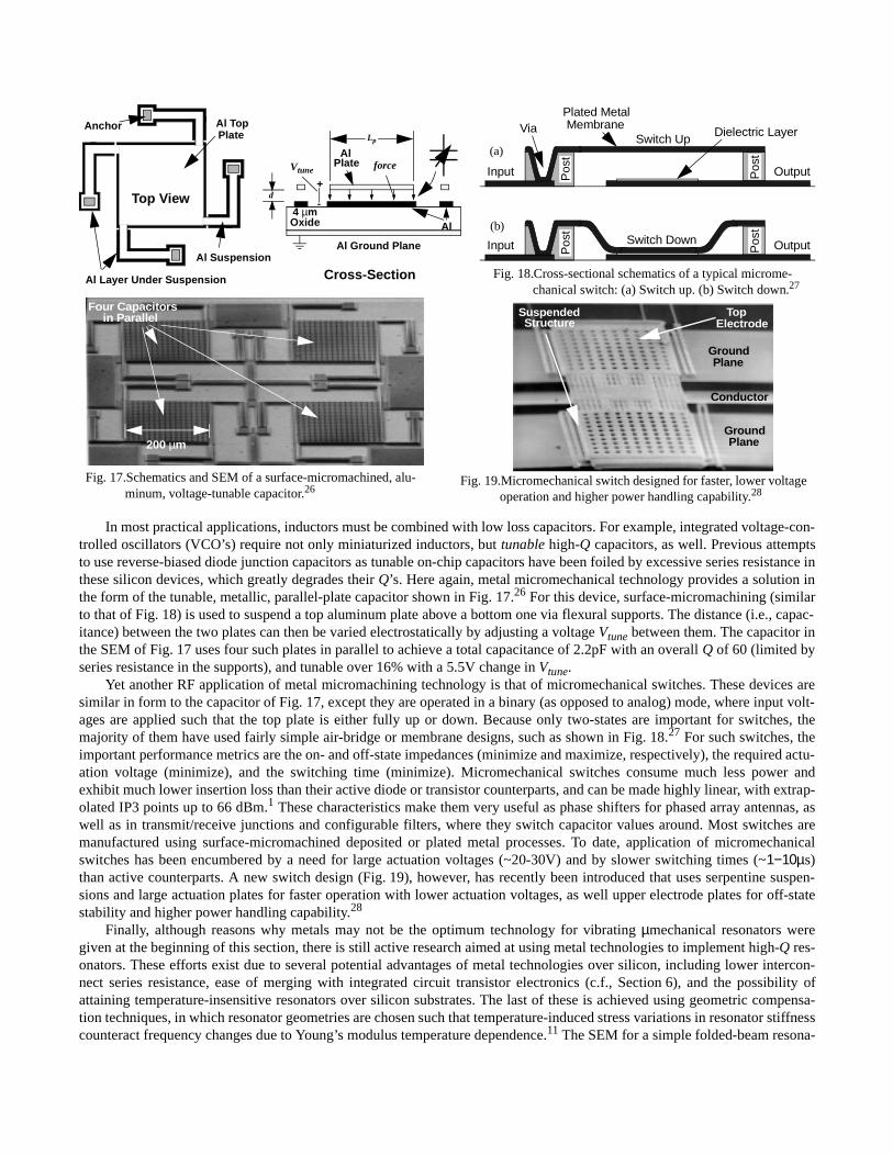
In most practical applications, inductors must be combined with low loss capacitors. For example, integrated voltage-con-trolled oscillators (VCO’s) require not only miniaturized inductors, but tunable high-Q capacitors, as well. Previous attemptsto use reverse-biased diode junction capacitors as tunable on-chip capacitors have been foiled by excessive series resistance inthese silicon devices, which greatly degrades their Q’s. Here again, metal micromechanical technology provides a solution inthe form of the tunable, metallic, parallel-plate capacitor shown in Fig. 17.26 For this device, surface-micromachining (similarto that of Fig. 18) is used to suspend a top aluminum plate above a bottom one via flexural supports. The distance (i.e., capac-itance) between the two plates can then be varied electrostatically by adjusting a voltage Vtune between them. The capacitor inthe SEM of Fig. 17 uses four such plates in parallel to achieve a total capacitance of 2.2pF with an overall Q of 60 (limited byseries resistance in the supports), and tunable over 16% with a 5.5V change in Vtune.
Yet another RF application of metal micromachining technology is that of micromechanical switches. These devices aresimilar in form to the capacitor of Fig. 17, except they are operated in a binary (as opposed to analog) mode, where input volt-ages are applied such that the top plate is either fully up or down. Because only two-states are important for switches, themajority of them have used fairly simple air-bridge or membrane designs, such as shown in Fig. 18.27 For such switches, theimportant performance metrics are the on- and off-state impedances (minimize and maximize, respectively), the required actu-ation voltage (minimize), and the switching time (minimize). Micromechanical switches consume much less power andexhibit much lower insertion loss than their active diode or transistor counterparts, and can be made highly linear, with extrap-olated IP3 points up to 66 dBm.1 These characteristics make them very useful as phase shifters for phased array antennas, aswell as in transmit/receive junctions and configurable filters, where they switch capacitor values around. Most switches aremanufactured using surface-micromachined deposited or plated metal processes. To date, application of micromechanicalswitches has been encumbered by a need for large actuation voltages (~20-30V) and by slower switching times (~1−10µs)than active counterparts. A new switch design (Fig. 19), however, has recently been introduced that uses serpentine suspen-sions and large actuation plates for faster operation with lower actuation voltages, as well upper electrode plates for off-statestability and higher power handling capability.28
Finally, although reasons why metals may not be the optimum technology for vibrating µmechanical resonators weregiven at the beginning of this section, there is still active research aimed at using metal technologies to implement high-Q res-onators. These efforts exist due to several potential advantages of metal technologies over silicon, including lower intercon-nect series resistance, ease of merging with integrated circuit transistor electronics (c.f., Section 6), and the possibility ofattaining temperature-insensitive resonators over silicon substrates. The last of these is achieved using geometric compensa-tion techniques, in which resonator geometries are chosen such that temperature-induced stress variations in resonator stiffnesscounteract frequency changes due to Young’s modulus temperature dependence.11 The SEM for a simple folded-beam resona-
TopElectrode
SuspendedStructure
GroundPlane
GroundPlane
Conductor
Fig. 17.Schematics and SEM of a surface-micromachined, alu-minum, voltage-tunable capacitor.26
Fig. 18.Cross-sectional schematics of a typical microme-chanical switch: (a) Switch up. (b) Switch down.27
Fig. 19.Micromechanical switch designed for faster, lower voltage operation and higher power handling capability.28
Four Capacitorsin Parallel
200 µm
Al Top
Al Suspension
Al Layer Under Suspension
AnchorPlate
Vtune
4 µmOxide
+
-
forceAl
Plate
Al Ground Plane
Al
d
Lp
Top View
Cross-Section
Switch Down OutputInput Pos
t
Pos
t
Switch Up
OutputInput Pos
t
Pos
t
Dielectric LayerViaPlated MetalMembrane
(a)
(b)
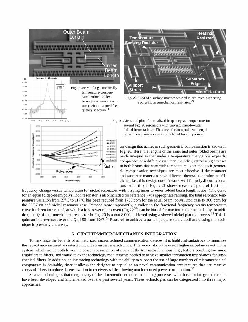
tor design that achieves such geometric compensation is shown inFig. 20. Here, the lengths of the inner and outer folded beams aremade unequal so that under a temperature change one expands/compresses at a different rate than the other, introducing stressesin both beams that vary with temperature. Note that such geomet-ric compensation techniques are most effective if the resonatorand substrate materials have different thermal expansion coeffi-cients; i.e., this design doesn’t work well for polysilicon resona-tors over silicon. Figure 21 shows measured plots of fractional
frequency change versus temperature for nickel resonators with varying inner-to-outer folded beam length ratios. (The curvefor an equal folded-beam polysilicon resonator is also included for reference.) Via appropriate ratioing, the total resonator tem-perature variation from 27oC to 117oC has been reduced from 1750 ppm for the equal beam, polysilicon case to 300 ppm forthe 50/57 ratioed nickel resonator case. Perhaps more importantly, a valley in the fractional frequency versus temperaturecurve has been introduced, at which a low power micro-oven (Fig.2229) can be biased for maximum thermal stability. In addi-tion, the Q of the µmechanical resonator in Fig. 20 is about 8,000, achieved using a slowed nickel plating process.11 This isquite an improvement over the Q of 90 from 1967.24 Research to achieve ultra-temperature stable oscillators using this tech-nique is presently underway.
6. CIRCUITS/MICROMECHANICS INTEGRATIONTo maximize the benefits of miniaturized micromachined communication devices, it is highly advantageous to minimize
the capacitance incurred via interfacing with transceiver electronics. This would allow the use of higher impedances within thesystem, which would both lower the power consumption of many of the transistor functions (e.g., buffers coupling low noiseamplifiers to filters) and would relax the technology requirements needed to achieve smaller termination impedances for µme-chanical filters. In addition, an interfacing technology with the ability to support the use of large numbers of micromechanicalcomponents is desirable, since it allows the designer to capitalize on novel communication architectures that use massivearrays of filters to reduce desensitization in receivers while allowing much reduced power consumption.30
Several technologies that merge many of the aforementioned micromachining processes with those for integrated circuitshave been developed and implemented over the past several years. These technologies can be categorized into three majorapproaches:
Fig. 22.SEM of a surface-micromachined micro-oven supporting a polysilicon µmechanical resonator.29
Outer BeamLength
InnerBeamLength
-55.00
-50.00
-45.00
-40.00
-35.00
-30.00
-25.00
-20.00
-15.00
65.90 66.00 66.10 66.20 66.30
Spectrum of Ni Resonator
k Hz
dB
Q=7932fo=66098.25
Fig. 20.SEM of a geometrically temperature-compen-sated ratioed folded-beam µmechanical reso-nator with measured fre-quency spectrum.11
SupportStruts
HeatingResistorTemperature
Sensing Resistor
Micro-Platform
SubstrateEdge
Fig. 21.Measured plot of normalized frequency vs. temperature for several Fig. 20 resonators with varying inner-to-outer folded-beam ratios.11 The curve for an equal beam length polysilicon µresonator is also included for comparison.
PolysiliconNickel

(1) Mixed Circuit and Micromechanics, in which steps from both the circuit and the micromachining processes are inter-mingled into a single flow. Of the three approaches, this one has so far seen the most use. However, it suffers fromtwo major drawbacks: (i) many passivation layers are required (one needed virtually every time the process switchesbetween circuits and micromechanics); and (ii) extensive re-design of the process is often necessary if one of thecombined technologies changes (e.g., a more advanced circuit process is introduced). Analog Devices’ BiMOSII pro-cess (Fig. 2312), which has successfully produced a variety of accelerometers in large volume, is among the most suc-cessful examples of mixed circuit/micromechanics processes.
(2) Pre-Circuits, in which micromechanics are fabricated in a first module, then circuits are fabricated in a subsequentmodule, and no process steps from either module are intermingled. This process has a distinct advantage over themixed process above in that advances in each module can be accommodated by merely replacing the appropriatemodule. Thus, if a more advanced circuit process becomes available, the whole merging process need not be re-designed; rather, the circuits module need only be replaced. An additional advantage is that only one passivation stepis required after the micromechanical module. One of the main technological hurdles in implementing this process isthe large topography leftover by micromechanical processes, with features that can be as high as 9 µm, dependingupon the number and geometry of structural layers. Such topographies can make photoresist spinning and patterningquite difficult, especially if submicron circuit features are desired. These problems, however, have been overcome byresearchers at Sandia National Laboratories, whose iMEMS process (Fig. 24) performs the micromechanics modulein a trench, then planarizes features using chemical mechanical polishing (CMP) before doing the circuits module.31
(3) Post-Circuits—the dual of pre-circuits—in which the circuits module comes first, followed by the micromechanicsmodule, where again, no process steps from either module are interspersed. This process has all the advantages ofpre-circuits, but with relaxed topography issues, since circuit topographies are generally much smaller than microme-chanical ones. As a result, planarization is often not necessary before micromechanics processing. Post-circuit pro-cesses have the additional advantage in that they are more amenable to multi-facility processing, in which a veryexpensive fabrication facility (perhaps a foundry) is utilized for the circuits module, and relatively lower capitalmicromechanics processing is done in-house at the company site (perhaps a small start-up). Such an arrangement
Fig. 23.Cross-section of the sensor area in Analog Devices’ BiMOSII process.12
Fig. 24.Cross-section of Sandia’s iMEMS process.31
Fig. 25.(a) Cross-section of the MICS process.32 (b) Overhead-view of a fully integrated micromechanical resonator oscil-lator fabricated using MICS.33
Sustaining
Ramp
VP
+
−
vi
io
Anchors
Folded-BeamSuspension
Comb-Transducer
ShuttleMass
Amplifier xy
(Input)
L
pwelln-substrate
Thermal SiO2
Ground Plane Polysilicon
Structural Polysilcion (Suspended Beams)
Si N3 4
2TiSiContact Barrier
TungstenInterconnect
Poly-to-Poly Capacitor
(b)
(a)
p-
n+ runner
thoxMetal
Air
Sensor Polysilicon
p
BPSG
Arsenic-DopedEpitaxial Layer
MechanicalPoly
PolyStud
PE Nitride
n-tubp-tub
Poly1 Metal1 Oxide
Nitride MM Poly0
n-type Substrate
may be difficult to achieve with a pre-circuits process because IC foundries may not permit “dirty” micromachinedwafers into their ultra-clean fabrication facilities. Unfortunately, some amount of technical innovation is still neededbefore post-circuits processes become practical. The main difficulty has been that aluminum based circuit metalliza-tion technologies cannot withstand subsequent high temperature processing required by many micromechanics pro-cesses—especially those that must achieve high Q. Thus, compromises in either the circuits process or themicromechanics process have been necessary, undermining the overall modularity of the process. The MICSprocess32 (Fig. 25), which used tungsten metallization instead of aluminum to withstand the high temperatures usedin a following polysilicon surface micromachining module, is a good example of a post-circuits process. Research inthis area is ongoing. The work to achieve nickel processes with adequate quality factor detailed in Section 5 is in factpartially driven by the desire to achieve a practical post-circuits process.
There are number of other processes that can to some extent be placed in more than one of the above categories. Theseinclude front bulk-micromachining processes similar to the single-crystal silicon process of Fig. 12 but using anisotropic wetetchants34 and other processes that slightly alter conventional CMOS processes.35 In addition, bonding processes, in whichcircuits and micromechanics are merged by bonding one onto the wafer of the other, are presently undergoing a resurgence. Inparticular, the advent of more sophisticated aligner-bonder instruments are now making possible much smaller bond pad sizes,which soon may enable wafer-level bonding with bond pad sizes small enough to compete with fully planar processed mergingstrategies in interface capacitance values. If the bond capacitance can indeed be lowered to this level with acceptable bondingyields, this technology would perhaps exhibit the most modularity of all.
7. ENCAPSULATIONFrom a broader perspective, the integration techniques discussed above are really methods for achieving low capacitance
packaging of microelectromechanical systems. From the discussion in Section 2, another level of packaging is required toattain high Q vibrating µmechanical resonators: vacuum encapsulation. Although the requirement for vacuum is unique tovibrating µmechanical resonators, the requirement for encapsulation is nearly universal for all of the micromechanical devicesdiscussed in this paper. In particular, some protection from the environment is necessary, if only to prevent contamination byparticles (or even by molecules), or to isolate the device from electric fields or feedthrough currents.
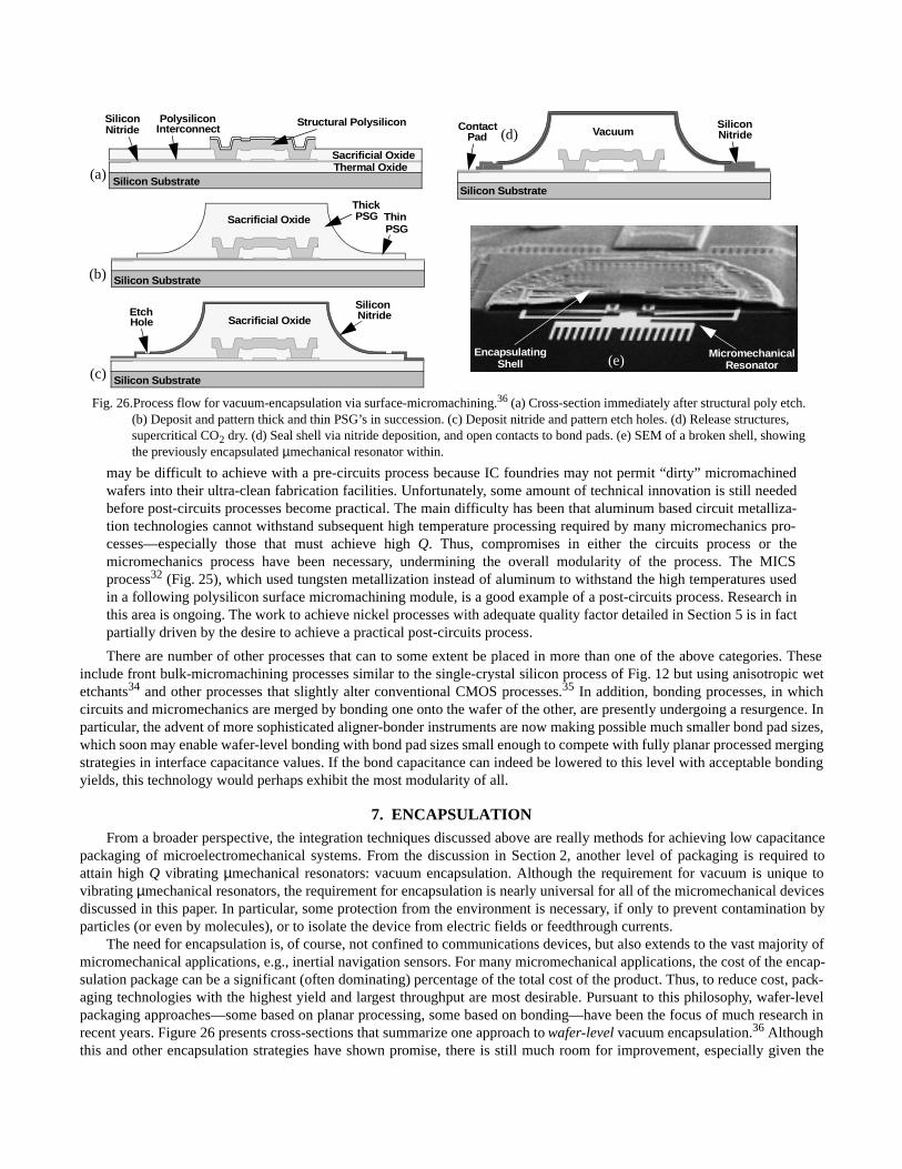
The need for encapsulation is, of course, not confined to communications devices, but also extends to the vast majority ofmicromechanical applications, e.g., inertial navigation sensors. For many micromechanical applications, the cost of the encap-sulation package can be a significant (often dominating) percentage of the total cost of the product. Thus, to reduce cost, pack-aging technologies with the highest yield and largest throughput are most desirable. Pursuant to this philosophy, wafer-levelpackaging approaches—some based on planar processing, some based on bonding—have been the focus of much research inrecent years. Figure 26 presents cross-sections that summarize one approach to wafer-level vacuum encapsulation.36 Althoughthis and other encapsulation strategies have shown promise, there is still much room for improvement, especially given the
Fig. 26.Process flow for vacuum-encapsulation via surface-micromachining.36 (a) Cross-section immediately after structural poly etch. (b) Deposit and pattern thick and thin PSG’s in succession. (c) Deposit nitride and pattern etch holes. (d) Release structures, supercritical CO2 dry. (d) Seal shell via nitride deposition, and open contacts to bond pads. (e) SEM of a broken shell, showing the previously encapsulated µmechanical resonator within.
Silicon SubstrateThermal Oxide
Structural Polysilicon
Sacrificial Oxide
Silicon Substrate
Sacrificial OxideThickPSG Thin
PSG
Silicon Substrate
Sacrificial OxideSiliconNitrideEtch
Hole
Silicon Substrate
VacuumSiliconNitride
ContactPad
PolysiliconInterconnectNitride
Silicon
MicromechanicalResonator
EncapsulatingShell
(a)
(b)
(c)
(d)
(e)
large percentage of total product cost attributed to the package alone. Research to reduce the cost (i.e., enhance the yield andthroughput) of encapsulation technologies continues.
8. CONCLUSIONSMicromechanical devices appear to be the perfect complements to active integrated circuit transistor devices in trans-
ceiver applications. In particular, transistor circuits excel at amplification, mixing, and digital processing, but are sorely defi-cient where frequency selectivity or high stability are required. Micromachined devices, on the other hand, excel at frequencyselectivity and high stability, making them ideal components with which to fill the void in transceiver function left by transis-tors. These considerations in combination with the obvious similarities between micromachining and integrated circuit tech-nologies—e.g., both are amenable to batch processing, both are based on wafer level deposition, lithography, and patterning—make an overwhelming case for research efforts aimed at merging the two technologies into a single wafer-level technology,perhaps someday capable of achieving a single-chip transceiver with all the sensitivity and link advantages of today’s super-heterodyne systems.
Is the application range for RF micromachining technologies confined to frequency selectivity and stability? Perhaps, not.Already, strategies for amplification, mixing, and digital processing via micromechanical means are under investigation, withthe objective of lowering power dissipation by several times—a must for miniature transceivers, considering the tiny batteriesthat will be used to power them. In this respect, the micromachining technologies described in this paper and the improve-ments to be made in the near future may very well hold the key to future transceiver revolution.
9. ACKNOWLEDGMENTSAside from automatically acknowledging all referenced material within this overview article, the author gratefully
acknowledges substantial contributions from former and present graduate students, in particular Kun Wang, Ark-Chew Wong,and Wan-Thai Hsu, who are largely responsible for the micromechanical resonator results. Research on micromechanical com-munications devices at the University of Michigan has been supported in part by grants from the Defense Advanced ResearchProjects Agency (DARPA), the National Science Foundation (NSF), NASA, and the Army Research Office (ARO), as well asnumerous industrial sponsors.
10. REFERENCES1. C. T.-C. Nguyen, L. P.B. Katehi, and G. M. Rebeiz, “Micromachined devices for wireless communications (invited),”
Proc. IEEE, vol. 86, no. 8, pp. 1756-1768, Aug. 1998.2. C. T.-C. Nguyen, “Micromechanical devices for wireless communications (invited),” Proceedings, 1998 IEEE Interna-
tional Workshop on Micro Electro Mechanical Systems, Heidelberg, Germany, Jan. 25-29, 1998, pp. 1-7.3. F. D. Bannon III, J. R. Clark, and C. T.-C. Nguyen, “High frequency microelectromechanical IF filters,” Technical
Digest, IEEE International Electron Devices Meeting, San Francisco, CA, Dec. 8-11, 1996, pp. 773-776.4. C. T.-C. Nguyen, “Frequency-selective MEMS for miniaturized communication devices (invited),” Proceedings, 1998
IEEE Aerospace Conference, Snowmass, Colorado, March 21-28, 1998, pp. 445-460.5. K. Wang, F. D. Bannon III, J. R. Clark, and C. T.-C. Nguyen, “Q-enhancement of micromechanical filters via low-veloc-
ity spring coupling,” to be published in the Proceedings of the 1997 IEEE International Ultrasonics Symposium, Toronto,Ontario, Canada, Oct. 5-8, 1997.
6. A. I. Zverev, Handbook of Filter Synthesis, New York: John Wiley & Sons, 1967.7. C. T.-C. Nguyen and R. T. Howe, “Quality factor control for micromechanical resonators,” Technical Digest, IEEE Inter-
national Electron Devices Meeting, San Francisco, California, December 14-16, 1992, pp. 505-508.8. W. E. Newell, “Miniaturization of tuning forks,” Science, vol. 161, pp. 1320-1326, Sept. 1968.9. K. Wang and C. T.-C. Nguyen, “High-order micromechanical electronic filters,” Proceedings, 1997 IEEE International
Micro Electro Mechanical Systems Workshop, Nagoya, Japan, Jan. 26-30, 1997, pp. 25-30.10. W. C. Tang, T.-C. H. Nguyen, M. W. Judy, and R. T. Howe, “Electrostatic-comb drive of lateral polysilicon resonators,”
Sensors and Actuators, vol. A21-23, pp. 328-331. 1990.11. W.-T. Hsu and C. T.-C. Nguyen, “Geometric stress compensation for enhanced thermal stability in micromechanical res-
onators,” to be published in the Proceedings of the 1998 IEEE International Ultrasonics Symposium, Sendai, Japan,Oct. 5-8, 1998.
12. T. A. Core, W. K. Tsang, S. J. Sherman, “Fabrication technology for an integrated surface-micromachined sensor,” SolidState Technology, pp. 39-47, Oct. 1993.
13. J. W. Weigold and S. W. Pang, “A New Frontside-Release Etch-Diffusion Process for the Fabrication of Thick Si Micro-
structures”, Proc. 9th Int. Conference on Solid State Sensors and Actuators (Transducers'97), Chicago, June 1997, pp.1435-1438.
14. E. E. Hui, C. G. Keller, R. T. Howe, “Carbonized parylene as a conformal sacrificial layer,” Technical Digest, 1998 Solid-State Sensor and Actuator Workshop, Hilton Head, SC, June 3-6, 1998, pp. 256-260.
15. S. V. Krishnaswamy, J. Rosenbaum, S. Horwitz, C. Yale, and R. A. Moore, “Compact FBAR filters offer low-loss perfor-mance,” Microwaves & RF, pp. 127-136, Sept. 1991.
16. A. N. Cleland and M. L. Roukes, “Fabrication of high frequency nanometer scale mechanical resonators from bulk Sicrystals,” Appl. Phys. Lett., 69 (18), pp. 2653-2655, Oct. 28, 1996.
17. N. Slawsby, “Frequency control requirements of radar,” Proceedings of the 1994 IEEE International Frequency ControlSymposium, June 1-3, 1994, pp. 633-640.
18. J. W. Weigold, A.-C. Wong, C. T.-C. Nguyen, and S. W. Pang, “Thick single crystal Si lateral resonant devices integratedwith a conventional circuit process”, Late News Supplemental Digest, 1988 Solid State Sensor and Actuator Workshop,Hilton Head, South Carolina, June 8-11, 1998, pp. 15-16.
19. G. T. A. Kovacs, N. I. Maluf, K. E. Petersen, “Bulk micromachining of silicon,” Proc. IEEE, vol. 86, no. 8, pp. 1536-1551, Aug. 1998.
20. A. R. Brown and G. M. Rebeiz, “Micromachined micropackaged filter banks”, Microwave and Guided Wave Letters, vol.8, pp. 158-160, March 1998.
21. G. M. Rebeiz, D. P. Kasilingam, Y. Guo, P. A. Stimpson, and D. B. Rutledge, “Monolithic millimeter-wave two-dimen-sional horn imaging arrays,” IEEE Trans. Antennas Propagat., vol. AP-38, pp. 1473-1482, Sept. 1990.
22. G. P. Gauthier, A. Courtay, and G. M. Rebeiz, “Microstrip antennas on synthesized low dielectric constant substrates,”IEEE Trans. Antennas Propag., vol. AP-45, pp. 1310-1314, Aug. 1997.
23. B. Ziaie, N. K. Kocaman, and K. Najafi, “A generic micromachined silicon platform for low-power, low-loss miniaturetransceivers,” Digest of Technical Papers, 1997 International Conference on Solid-State Sensors and Actuators (Trans-ducers’97), Chicago, Illinois, June 16-19, 1997, pp. 257-260.
24. H. Nathanson, W. E. Newell, R. A. Wickstrom, and J. R. Davis, Jr., “The resonant gate transistor,” IEEE Trans. ElectronDevices, vol. ED-14, No. 3, pp. 117-133, March 1967.
25. D. J. Young, V. Malba, J.-J. Ou, A. F. Bernhardt, and B. E. Boser, “Monolithic high-performance three-dimensional coilinductors for wireless communication applications,” Technical Digest, IEEE International Electron Devices Meeting,Washington, D. C., Dec. 8-11, 1997, pp. 67-70.
26. D. J. Young and B. E. Boser, “A micromachined variable capacitor for monolithic low-noise VCOs,” Technical Digest,1996 Solid-State Sensor and Actuator Workshop, Hilton Head Island, South Carolina, June 3-6, 1996, pp. 86-89.
27. C. Goldsmith, J. Randall, S. Eshelman, T. H. Lin, D. Denniston, S. Chen and B. Norvell, “Characteristics of microma-chined switches at microwave frequencies,” IEEE MTT-S Digest, June, 1996, pp. 1141-1144.
28. S. Pacheco, C. T.-C. Nguyen, and L. P. B. Katehi, “Micromechanical electrostatic K-band switches,” Proceedings, IEEEMTT-S International Microwave Symposium, Baltimore, Maryland, June 7-12, 1998, pp. 1569-1572.
29. C. T.-C. Nguyen and R. T. Howe, “Microresonator frequency control and stabilization using an integrated micro oven,”Digest of Technical Papers, the 7th International Conference on Solid-State Sensors and Actuators (Transducers’93),Yokohama, Japan, June 7-10, 1993, pp. 1040-1043.
30. C. T.-C. Nguyen, “Communications applications of microelectromechanical systems (invited),” to be published in theProceedings of Sensors Expo, San Jose, California, May 20, 1998.
31. J. H. Smith, S. Montague, J. J. Sniegowski, J. R. Murray, et al., “Embedded micromechanical devices for the monolithicintegration of MEMS with CMOS,” Proceedings, IEEE International Electron Devices Meeting, Washington, D.C., Dec.10-13, 1995, pp. 609-612.
32. J. M. Bustillo, G. K. Fedder, C. T.-C. Nguyen, and R. T. Howe, “Process technology for the modular integration ofCMOS and polysilicon microstructures,” Microsystem Technologies, 1 (1994), pp. 30-41.
33. C. T.-C. Nguyen and R. T. Howe, “CMOS Micromechanical Resonator Oscillator,” Technical Digest, IEEE InternationalElectron Devices Meeting, Washington, D. C., December 5-8, 1993, pp. 199-202.
34. H. Baltes, O. Paul, and O. Brand, “Micromachined thermally based CMOS microsensors,” Proc. IEEE, vol. 86, no. 8, pp.1660-1678, Aug. 1998.
35. G. K. Fedder, S. Santhanam, M. L. Reed, S. C. Eagle, D. F. Guillou, M. S.-C. Lu, and L. R. Carley, “Laminated high-aspect-ratio microstructures in a conventional CMOS process,” Sensors and Actuators, vol. A57, no. 2, pp. 103-110,March 1997.
36. L. Lin, K. M. McNair, R. T. Howe, and A. P. Pisano, “Vacuum-encapsulated lateral microresonators,” Digest of Techni-cal Papers, the 7th International Conference on Solid-State Sensors and Actuators (Transducers’93), Yokohama, Japan,June 7-10, 1993, pp. 270-273.