MIC-3612 Manual 1st ed - ProSoft · PDF fileHARDWARE CONFIGURATION ... The MIC-3612 is a 3U/6U...
28
Copyright Notice This document is copyrighted 2002. All rights are reserved. The original manufacturer reserves the right to make improvements to the products described in this manual at any time without notice. No part of this manual may be reproduced, copied, translated or transmitted in any form or by any means without the prior written permission of the original manufacturer. Information provided in this manual is intended to be accurate and reliable. However, the original manufacturer assumes no responsibility for its use, nor for any infringements upon the rights of third parties which may result from its use. Acknowledgments PC-LabCard is a trademark of Advantech Co., Ltd. IBM and PC are trademarks of International Business Machines Corporation. MS-DOS, Windows® , Microsoft ® Visual C++ and Visual BASIC are trademarks of Microsoft ® Corporation. Intel ® and Pentium ® are trademarks of Intel Corporation. Delphi and C ++ Builder are trademarks of Inprise Corporation. CE notification The MIC-3612, developed by ADVANTECH CO., LTD., has passed the CE test for environmental specifications when shielded cables are used for external wiring. We recommend the use of shielded cables. This kind of cable is available from Advantech. Please contact your local supplier for ordering information. On-line Technical Support For technical support and service, please visit our support website at: http://www.advantech.com/support Part No.2003361200 1st Edition Printed in Taiwan December 2002
Transcript of MIC-3612 Manual 1st ed - ProSoft · PDF fileHARDWARE CONFIGURATION ... The MIC-3612 is a 3U/6U...

Copyright Notice
This document is copyrighted 2002. All rights are reserved. The original manufacturer reserves the right to make improvements to the products described in this manual at any time without notice. No part of this manual may be reproduced, copied, translated or transmitted in any form or by any means without the prior written permission of the original manufacturer. Information provided in this manual is intended to be accurate and reliable. However, the original manufacturer assumes no responsibility for its use, nor for any infringements upon the rights of third parties which may result from its use.
Acknowledgments
PC-LabCard is a trademark of Advantech Co., Ltd. IBM and PC are trademarks of International Business Machines Corporation. MS-DOS, Windows® , Microsoft® Visual C++ and Visual BASIC are trademarks of Microsoft®
Corporation. Intel® and Pentium® are trademarks of Intel Corporation. Delphi and C++ Builder are trademarks of Inprise Corporation.
CE notification
The MIC-3612, developed by ADVANTECH CO., LTD., has passed the CE test for environmental specifications when shielded cables are used for external wiring. We recommend the use of shielded cables. This kind of cable is available from Advantech. Please contact your local supplier for ordering information.
On-line Technical Support
For technical support and service, please visit our support website at: http://www.advantech.com/support
Part No.2003361200 1st Edition
Printed in Taiwan December 2002

Contents
GENERAL INFORMATION .............................................................................................................................1
1.1 INTRODUCTION...........................................................................................................................................2 1.2 FEATURES.....................................................................................................................................................2 1.3 SPECIFICATIONS..........................................................................................................................................3
HARDWARE CONFIGURATION....................................................................................................................5
2.1 INITIAL INSPECTION ...................................................................................................................................6 2.2 HARDWARE INSTALLATION.......................................................................................................................7 2.3 I/O ADDRESS AND INTERRUPT SETUP.....................................................................................................9 2.4 BOARD LAYOUT: DIMENSIONS...............................................................................................................10 2.5 JUMPER SETTING......................................................................................................................................11
PIN ASSIGNMENT & WIRING..................................................................................................................... 15
3.1 PIN ASSIGNMENTS.....................................................................................................................................16
REGISTER STRUCTURE............................................................................................................................... 21
4.1 REGISTER STRUCTURE.............................................................................................................................22

1
Ch
apte
r
1 General Information

2
1.1 Introduction The MIC-3612 is a 3U/6U sized 4-port RS-232/422/485 CompactPCI® Comm. Card, serial communication cards which complies with PICMG 2.0 R2.1 CompactPCI specifications. All channels are addressed in a continuous 32 byte I/O block for simplified software access. All channels may also share one PCI interrupt. An interrupt status register is available for determining the interrupt source. The MIC-3612 comes standard with 16C954 UARTs containing 128 byte FIFOs. These upgraded FIFOs greatly reduce CPU overhead and are an ideal choice for heavy multitasking environments.
1.2 Features • PCI Specification 2.1x compliant • Speeds up to 921.6 Kbps • 16C954 UARTs with 128-byte standard • Standard Industrial 3U/6U sized CPCI Board size • I/O address automatically assigned by PCI Plug-and-Play • OS supported: Windows98, Windows NT, Windows 2000, Windows XP • Surge protection (2500VDC). • Interrupt status register for increased performance • Space reserved for termination resistors (for RS-422/485) • Automatic RS-485 data flow control
3
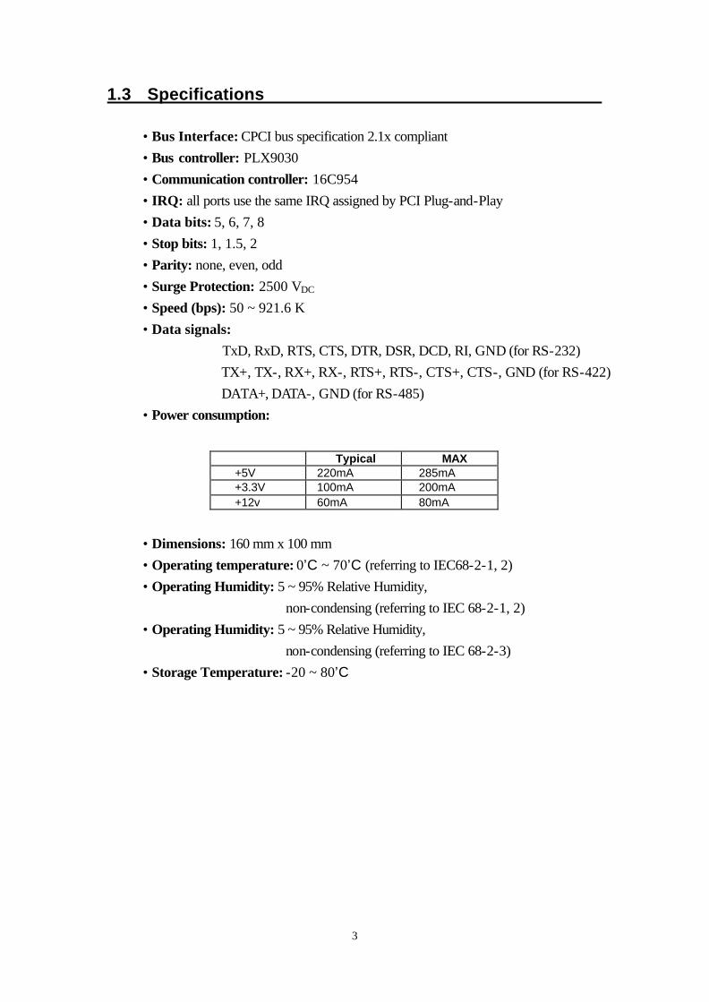
1.3 Specifications • Bus Interface: CPCI bus specification 2.1x compliant • Bus controller: PLX9030 • Communication controller: 16C954 • IRQ: all ports use the same IRQ assigned by PCI Plug-and-Play • Data bits: 5, 6, 7, 8 • Stop bits: 1, 1.5, 2 • Parity: none, even, odd • Surge Protection: 2500 VDC • Speed (bps): 50 ~ 921.6 K • Data signals:
TxD, RxD, RTS, CTS, DTR, DSR, DCD, RI, GND (for RS-232) TX+, TX-, RX+, RX-, RTS+, RTS-, CTS+, CTS-, GND (for RS-422) DATA+, DATA-, GND (for RS-485)
• Power consumption:
• Dimensions: 160 mm x 100 mm • Operating temperature: 0’C ~ 70’C (referring to IEC68-2-1, 2) • Operating Humidity: 5 ~ 95% Relative Humidity,
non-condensing (referring to IEC 68-2-1, 2) • Operating Humidity: 5 ~ 95% Relative Humidity,
non-condensing (referring to IEC 68-2-3) • Storage Temperature: -20 ~ 80’C
Typical MAX +5V 220mA 285mA +3.3V 100mA 200mA +12v 60mA 80mA

4

5
2 Hardware Configuration
Ch
apte
r

6
This chapter gives users a package item checklist, proper instructions about unpacking and step-by-step procedures for card installation.
2.1 Initial Inspection In addition to this manual, you should find the following items inside the shipping package of the MIC-3612: • CPCI communication interface card • Advantech Automation Software CD-ROM • CPCI communication card user's manual • Wiring cable We have carefully inspected the CPCI communication card series before shipping it. It should be free of marks and scratches and in perfect working order on receipt. As you unpack the CPCI communication card series, check it for signs of shipping damage (damaged box, scratches, dents, etc.). If it is damaged or it fails to meet specifications, notify our service department or your local sales representative immediately. Also notify the carrier. Retain the shipping carton and packing material for inspection by the carrier. After inspection we will make arrangements to repair or replace the unit. When you handle the CPCI communication card series, remove it from its protective packaging by grasping the rear metal panel. Keep the anti-vibration packaging. Whenever you remove the card from the PC, store it in this package for protection.
Note: Discharge your body’s static electric charge by touching the back of the grounded chassis of the system unit (metal) before handling the board. You should avoid contact with materials that hold a static charge such as plastic, vinyl and styrofoam. Handle the board only by its edges to avoid static damage to its integrated circuits. Avoid touching the exposed circuit connectors. We also recommend that you use a grounded wrist strap and place the card on a static dissipative mat whenever you work with it.

7
2.2 Hardware Installation Note
Make sure you have installed the driver first before installing the card
(Please refer to the software installation in Chapter 3 Driver Setup & Installation).
When you install the MIC-3612 Card, be sure the DLL driver of the MIC-3612 installation is complete, you can now go on to install the MIC-3612 card in your CPCI computer. But it is suggested that you should refer to the computer user manual or related documentation if you have any doubt. Please follow the steps below to install the card on your system.
To install a card:
Step 1: Remove one cover on the unused slot of your CPCI computer slot.
Step 2: Hold the Card Vertically. Be sure that the card is pointing in the correct
direction. The components of the card should be pointing to the right-hand side
and the black handle of the card should be pointing to lower edge of the
chassis.
Step 3: Holding the lower handle, pull the handle down to unlock it.
Step 4: Insert the MIC-3612 card into the CPCI chassis carefully by sliding the lower
edges of the card into the card guides.
Step 5: Please push the card into slot gently by sliding the card along the card guide
until J1 meets the long needle on the backplane.
Note If your card is correctly positioned and has been slid all the way into the chassis, the
handle should match the rectangular holes. If not, remove the card from the card guide and repeat step 3 again. Do not try to install a card by forcing it into the chassis.
Step 6: Push the card into the right place; secure the card by pushing the handle on to lock it into place.
Note The Blue LED on the front panel details the installation status of the card while the system is on. In step 5, when J1 meets the long needle on the backplane, Blue LED will light; after step 6, the system can configure the card automatically, and the Blue LED is turned off when the system finished the device configuration. If the system power is off, you can install the card step by step without attending Blue LED’s state.

8
To remove a card: Step 1: Push the handle down to unlock the card, then the CPCI system will
automatically uninstall the card configuration.
Step 2: Once the system finished the device configuration, the Blue LED on the front
panel will turn on. Now you can slide the card out.
Note 1 Advantech MIC-3612’s “Hot-Swap” function complies with CPCI Hot Swap Specification PICMG 2.1 R2.0.
Note 2 Because of the “Hot-Swap”, the above steps detail the card removal process while the system is on. If the system power is off, please follow step1 and step2 and disregard the status of the Blue LED.

9
2.3 I/O Address and Interrupt Setup In this section, you will learn to set an I/O base address for the MIC-3612. Base address setting
When the MIC-3612 is installed in the system or if the machine is first turned on, the configuration software must scan the various buses in the system. If the software locates the MIC-3612, the system will configure the device based on the parameters of the PCI device configuration registers, including the I/O base address, I/O range, memory base address, memory range, and so forth. The I/O base address is the base address on the four ports of the MIC-3612 card. The four ports address and interrupt register setting are as shown:
Base Address Setting CH 1 Base Add. + 00H CH 2 Base Add. + 08H CH 3 Base Add. + 10H CH 4 Base Add. + 18H Interrupt Register Base Add. + 62H
Interrupt Register The four-port interrupt belongs to the share interrupt mode. Read the register to achieve current interrupt status of all 4 channels. Active high indicates that interrupt is dependent on which channel.
Interrupt Register (Base Add. + 62H)
Bit Function 0 CH 1 1 CH 2 2 CH 3 3 CH 4 4 Not Used 5 Not Used 6 Not Used 7 Not Used

10
2.4 Board Layout: Dimensions
Figure 2-1: MIC-3612 board layout: Dimensions

11
2.5 Jumper Setting
This section provides the card default configuration and the options for setting each jumper.
How to set jumpers
You configure your card to match the needs of your application by setting the jumpers. A jumper is the simplest kind of electric switch. It consists of two metal pins and a small metal clip (often protected by a plastic cover) that slides over the pins to connect them. To “close” a jumper you connect the pins with the clip. To “open” a jumper you remove the clip. Sometimes a jumper will have three pins, labeled 1, 2 and 3. In this case you would connect either pins 1 and 2 or 2 and 3. You may find a pair of needle-nose pliers for setting the jumpers. If you have any doubts about the best hardware configuration for your application, contact your local distributor or sales representative before you make any changes.
Jumper setting example
Default Settings The board is shipped with default settings (all ports are set to RS-485 mode with
300O terminator resistors). If you need to change these settings, however, see the
following sections. Otherwise, you can simply install the card.
For MIC-3612, each port can support three operation modes, RS-232,
RS-485 and RS-422. l RS-232 mode
For RS-232 operation mode, set the jumper group U1 (U2,U8,U9) for Port 1 (2,3,4) to the RS-232 available position.
l RS-485 mode For RS-485 operation mode, users will have to use the following list to set the jumpers.
1. Jumper group U1 (U2,U8,U9) for Port 1 (2,3,4) to the RS-422/485.

12
2. Jumper JP1 (JP2,JP3,JP4) for Port 1(2,3,4) to the RS-485.
RS-422
RS-485
RS-485
3. DIP switch S1 have to switch to “AUTO” for RS-485 mode
CH1 CH2 CH3 CH4
ON ON ON ON ON OFF AUTO AUTO AUTO AUTO
l RS-422 Master mode
For RS-422 Master mode, the RS-422 Tx signal will always be enabled. For this
mode, users will have to use the following list to set the jumpers.
1. Jumper group U1 (U2,U8,U9) for Port 1 (2,3,4) to the RS-422/485.
2. Jumper JP1(JP2,JP3,JP4) for Port 1(2,3,4) to the RS-422.
RS-422
RS-485
RS-422
3. For RS-422 Master mode, DIP switch S1 will have to be “ON”
CH1 CH2 CH3 CH4
ON ON ON ON ON OFF AUTO AUTO AUTO AUTO

13
l RS-422 Slave mode For RS-422 Slave mode, the RS-422 Tx signal will be auto-enabled to send the data.
To set this mode, users will have to use the following list to set the jumpers.
1. Jumper group U1 (U2,U8,U9) for Port 1 (2,3,4) to the RS-422/485.
2. Jumper JP1(JP2,JP3,JP4) for Port 1(2,3,4) to the RS-422.
RS-422
RS-485
RS-422
3. For RS-422 Slave mode, DIP switch S1 will have to be switched to “AUTO”
CH1 CH2 CH3 CH4
ON ON ON ON ON OFF AUTO AUTO AUTO AUTO
Terminator resistor setup (JP4~JP12) In the RS485/422 mode, you can install terminator resistors to match line impedance.
For each signal line Tx (Data), Rx will have to be a separate resistor 120O or 300O .
For more details about jumper locations please refer to Figure 2-1.

14

15
3 Pin Assignment &
Wiring
Ch
apte
r

16
3.1 Pin assignments
The following diagrams show the pin assignments for the MIC-3612 DB44P connector.
RS-232 Mode
The MIC-3612 has 4 RS-232 ports. The following lists the pin assignments of the DB44 connector on the bracket. You may fabricate the cable for DB44 to 4 x DB9 with these output pin.
Pin No. Signal Pin No. Signal Pin No. Signal 1 TX0 17 DTR0 3 RTS0 2 RX0 18 DSR0 16 CTS0 31 DCD0 32 RI0 33 GND 5 TX1 21 DTR1 7 RTS1 6 RX1 22 DSR1 20 CTS1 35 DCD1 36 RI1 37 GND 9 TX2 25 DTR2 11 RTS2 10 RX2 26 DSR2 24 CTS2 39 DCD2 40 RI2 41 GND 13 TX3 29 DTR3 15 RTS3 14 RX3 30 DSR3 28 CTS3 42 DCD3 43 RI3 44 GND
Table 3-1: MIC-3612 DB44 Connector Pin Assignment for RS-232 Mode
The Table 3-2 is the description of DB9P male connector.
Signal Name Pin# Mode GND Ground 5 TX Transmit Data 3 Output
DTR Data Terminal Ready 4 Output RTS Request To Send 7 Output RX Receive Data 2 Input
DSR Data Set Ready 6 Input CTS Clear To Send 8 Input DCD Data Carrier Detect 1 Input RI Ring Indicator 9 Input
Table 3-2: RS232 Mode DB9 Male Connector Description

17
Figure 3-1: MIC-3612 DB44 Connector RS-232 Mode
RS-485 Mode The MIC-3612 has 4 RS-485 ports. The following lists the pin assignments for the
DB44 connectors on the bracket. You may copy the octopus cable for DB44 to 4 x
DB9 with these output pin.
Pin No. Signal Pin No. Signal Pin No. Signal
2 DATA0+ 31 DATA0- 33 GND 6 DATA1+ 35 DATA1- 37 GND
10 DATA2+ 39 DATA2- 41 GND 14 DATA3+ 42 DATA3- 44 GND
Table 3-3: MIC-3612 DB44 Connector Pin Assignment for RS-485 Mode
The Table 3-2 is the description of DB9P male connector.
Signal Name Pin# GND Ground 5
DATA- Transmit Data 1 DATA+ Data Terminal Ready 2
Table 3-4:RS-485 Mode DB9P Male Connector Description

18
Figure 3-1: MIC-3612 DB44 Connector RS-232 Mode
RS-422
MIC-3612 has 4 RS-422 ports. The following lists the pin assignments of the DB44
connector on the bracket. You may fabricate octopus cable for DB44 to 4 x DB9 with
these output pin.
Pin No. Signal Pin No. Signal Pin No. Signal
2 TX0+ 3 RTS0+ 33 GND 31 TX0- 18 RTS0- 1 RX0+ 16 CTS0+ 17 RX0- 32 CTS0- 6 TX1+ 7 RTS1+ 37 GND 35 TX1- 22 RTS1- 5 RX1+ 20 CTS1+ 21 RX1- 36 CTS1- 10 TX2+ 11 RTS2+ 41 GND 39 TX2- 26 RTS2- 9 RX2+ 24 CTS2+ 25 RX2- 40 CTS2- 14 TX3+ 15 RTS3+ 44 GND 42 TX3- 30 RTS3- 13 RX3+ 28 CTS3+ 29 RX3- 43 CTS3-
Table 3-5: MIC-3612 DB44 Connector Pin Assignment for RS-422 Mode

19
The Table 3-6 is the description of DB9P male connector.
Signal Name Pin# GND Ground 5 TX+ Transmit Data+ 2 TX- Transmit Data- 1 RX+ Receive Data+ 3 RX- Receive Data- 4
RTS+ Request To Send+ 7 RTS- Request To Send- 6 CTS+ Clear To Send+ 8 CTS- Clear To Send- 9
Table 3-6:RS-422 Mode DB9 Male Connector Description
Figure 3-3: MIC-3612 DB44 Connector RS-422 Mode

20

21
4 Register Structure
Ch
apte
r

22
4.1 Register Structure This chapter gives short descriptions of each of the module's registers. For more information please refer to the data book for the OX16C954 UART chip. All registers are one byte. Bit 0 is the least significant bit, and bit 7 is the most significant bit. The address of each register is specified as an offset from the port base address (BASE). DLAB is the "Divisor Latch Access Bit, bit 7 of BASE+3. BASE+0 Receiver buffer register when DLAB=0 and the operation is a read. BASE+0 Transmitter holding register when DLAB=0 and the operation is a write. BASE+0 Divisor latch bits 0 - 7 when DLAB=1. BASE+1 Divisor latch bits 8 - 15 when DLAB=1 The two bytes BASE+0 and BASE+1 together form a 16-bit number, the divisor, which determines the baud rate together with the values of TCR and CPR and Bit7 of MCR(Modem Control Register) (refer to 16C954 datasheet). The formula to set BaudRate as follows:
In formula, SC is sample clock value defined by TCR, when TCR=0x00, SC =16. Prescaler is defined by MCR[7] and CPR. Prescaler = 1 when MCR[7] = ‘0’; Prescaler = M+(N / 8), when MCR[7] =‘1’,
where: M = CPR[7:3] (Integer part – 1 to 31) N = CPR[2:0] (Fractional part – 0.000 to 0.875 )
While Bit7 of MCR is Logic”1”, TCR=0x00 and CPR=0x40, set the divisor as follows:
Baudrate Divisor Baudrate Divisor 50 2304 3600 32 75 1536 4800 24
150 768 7200 16 300 384 9600 12 600 192 19200 6 1200 96 38400 3 1800 64 57600 2 2400 48 115200 1
Table 4-1

23
Else, while Bit7 of MCR is Logic”0”, TCR=0x00, set the divisor as follows:
Baudrate Divisor 230400 4 307200 3 460800 2 921600 1
Table 4-2
BASE+1 Interrupt Enable Register (IER) when DLAB=0
Bit0 Enables received-data-available interrupt
Bit1 Enables transmitter-holding-register-empty interrupt
Bit2 Enables receiver-line-status interrupt
Bit3 Enables modem-status interrupt
Register
Mode 650/950 Mode 550/750 Mode
Bit4 Sleep mode Bit5 Special Char detect Alternate sleep mode Bit6 CTS Interrupt mask Bit7 RTS Interrupt Mask
Unused
Table 4-3
BASE+2 (read) Interrupt status register (ISR)
Register ISR
Bit0 Interrupt pending Bit1 Bit2 Bit3
Interrupt priority (All modes)
Bit4 Bit5 Interrupt priority (Enhanced mode)
Bit6 Bit7 FIFOs enabled
Table 4-4

24
Level Interrupt source ISR[5:0] see note 3
- No interrupt pending 1 000001
1 Receiver status error or Address-bit detected in 9-bit mode 000110
2a Receiver data available 000100 2b Receiver time-out 001100 3 Transmitter THR empty 000010 4 Modem status change 000000
5 2 In-band flow control XOFF or Special character (XOFF2) or Special character 1, 2, 3 or 4 or bit 9 set in 9-bit mode
010000
6 2 CTS or RTS change of state 100000
Table 4-5: Interrupt Status Identification Codes
Note 1. ISR[0] indicates whether any interrupts are pending. 2. Interrupts of priority levels 5 and 6 cannot occur unless the UART is in Enhanced mode. 3. ISR[5] is only used in 650 & 950 modes. In 750 mode, it is ‘0’ when FIFO size is 16 and
‘1’ when FIFO size is 128. In all other modes it is permanently set to 0
BASE+2 (write) FIFO Control Register (FCR)
Bit0 Enables transmit and receive FIFO
Bit1 Clears contents of receive FIFO
Bit2 Clears contents of transmit FIFO
Bits6-7 Sets trigger level for receiver FIFO interrupt.
Bit 7 Bit 6 FIFO Trigger Level
0 0 16 0 1 32 1 0 112 1 1 120
Table 4-6
BASE+3 Line Control Register (LCR)
Bit 0 Word length select bit 0
Bit 1 Word length select bit 1
Bit 2 Number of stop bits
Bit 3 Parity enable
Bit 4 odd/even parity select
Bit 5 Force parity
Bit 6 Tx break
Bit 7 Divisor Latch Access Bit (DLAB)

25
Bit 1 Bit 0 Word Length(bits)
0 0 5 0 1 6 1 0 7 1 1 8
Table 4-7
BASE+4 Modem Control Register (MCR)
Bit 0 DTR
Bit 1 RTS
Bit 3 Interrupt enable by software Bit 7 Baud prescale select
BASE+5 Line Status Register (LSR)
Bit 0 Receiver data ready
Bit 1 Overrun error
Bit 2 Parity error
Bit 3 Framing error
Bit 4 Breaks interrupt
Bit 5 Transmitter holding register empty
Bit 6 Transmitter shift register empty
Bit 7 At least one parity error, framing error or break indication on FIFO
BASE+6 Modem Status Register (MSR)
Bit 0 Delta CTS
Bit 1 Delta DSR
Bit 2 Trailing edge ring indicator
Bit 3 Delta received line signal detect
Bit 4 CTS
Bit 5 DSR
Bit 6 RI
Bit 7 DCD
BASE+7 Temporary data register and indexed control
Register offset value bits

26
Register to select auto 485 mode
Each UART in OX16c954 has one ACR register (Additional control register), Bits [4:3] in which it is used to set auto 485 mode with hardware circuit of MIC-3612. The ACR register is one register located at offset 0x00 of the 16c954’s Indexed Control Register. Set “11” to Bits[4:3] of this register to select auto 485 mode and “00” to select compatible with 16C450, 16C550,16C650 and 16C750. For more information on configuring the ACR, please refer to the data sheet of OX16C954 UART chip.
Interrupt Vector Register
MIC-3612 has an interrupt vector register. It is outside logic circuit from UARTs and the address of register is BASE+62H. Read the register to achieve current interrupt status of all 8 channels. Active high, to indicate that interrupt is pending in which channel.