
MENA3100 Scanning Electron Microscopy (SEM) Anders Werner Bredvei Skilbred Harald Fjeld.
44
MENA3100 Scanning Electron Microscopy (SEM) Anders Werner Bredvei Skilbred Harald Fjeld
-
Upload
stacey-wailes -
Category
Documents
-
view
273 -
download
19
Transcript of MENA3100 Scanning Electron Microscopy (SEM) Anders Werner Bredvei Skilbred Harald Fjeld.
MENA3100
Scanning Electron Microscopy (SEM)
Anders Werner Bredvei Skilbred Harald Fjeld
MENA3100
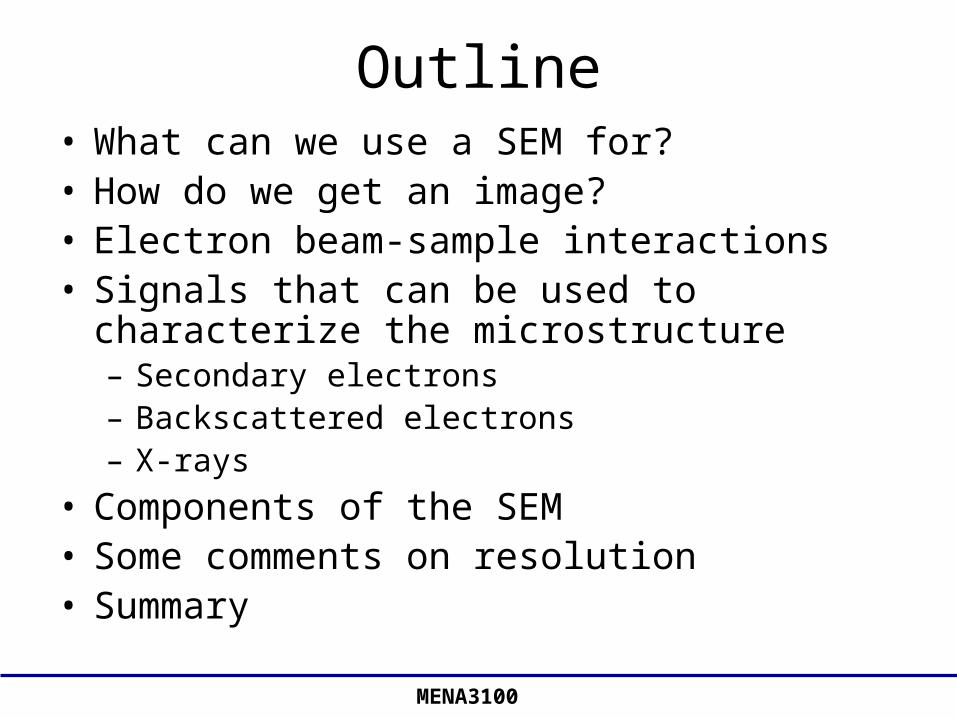
Outline• What can we use a SEM for?• How do we get an image?• Electron beam-sample interactions• Signals that can be used to characterize the
microstructure– Secondary electrons– Backscattered electrons– X-rays
• Components of the SEM• Some comments on resolution• Summary

MENA3100
The most versatile instrument for a materials scientist?
What can we study in a SEM?
• Topography and morphology
• Chemistry
• Crystallography
• Orientation of grains
• In-situ experiments:– Reactions with atmosphere– Effects of temperature
“Easy” samplepreparation!!
“Big” samples!

MENA3100
Topography and morphology
• High depth of focus
Image: Camilla Kongshaug, UiOImage: Christian Kjølseth, UiO

MENA3100
Depth of focus
Optical microscopy vs SEM
• A SEM typically has orders of magnitude better depth of focus than a optical microscope making SEM suitable for studying rough surfaces
• The higher magnification, the lower depth of focus
Screw length: ~ 0.6 cm
Images: the A to Z of Materials

MENA3100
Ce
Fe Sr
Chemistry Images: Harald Fjeld, UiO

MENA3100
In-situ imaging• A modern SEM can be equipped with various
accessories, e.g. a hot stage
MENA3100
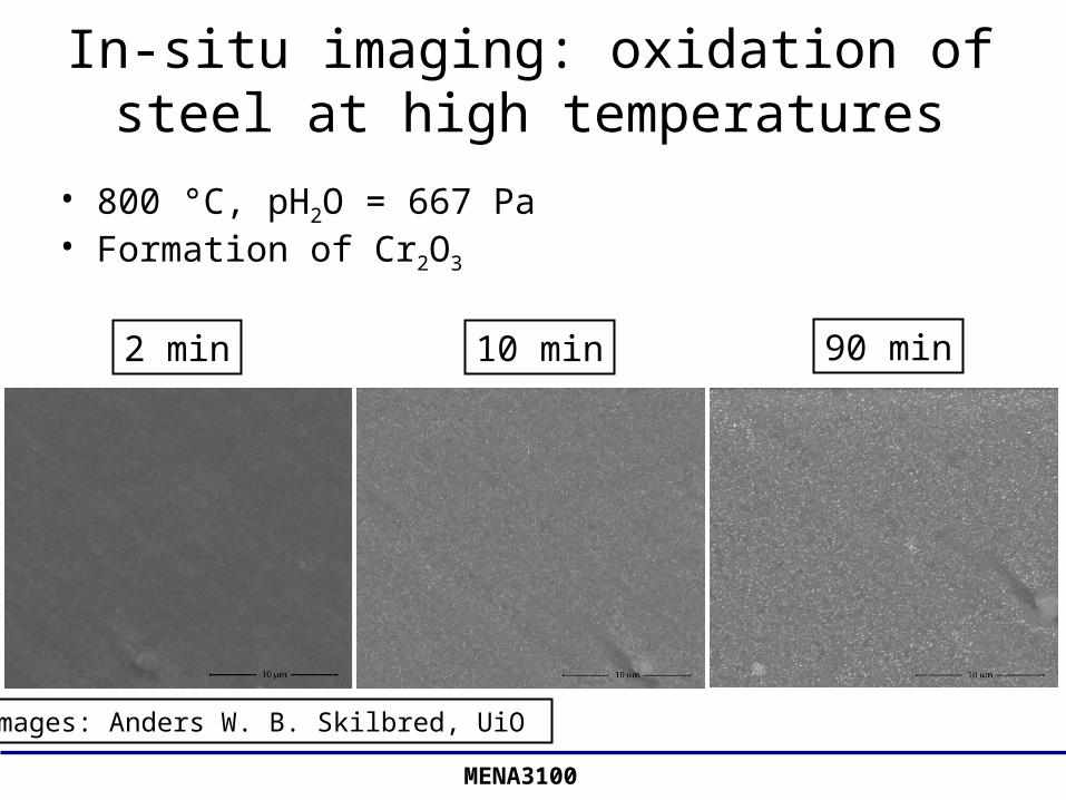
In-situ imaging: oxidation of steel at high temperatures
• 800 °C, pH2O = 667 Pa• Formation of Cr2O3
Images: Anders W. B. Skilbred, UiO
2 min 10 min 90 min

MENA3100
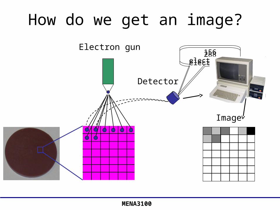
How do we get an image?
• In brief: we shoot high-energy electrons and analyze the outcoming electrons/x-rays
Electrons inElectrons out
or: x-rays out
MENA3100
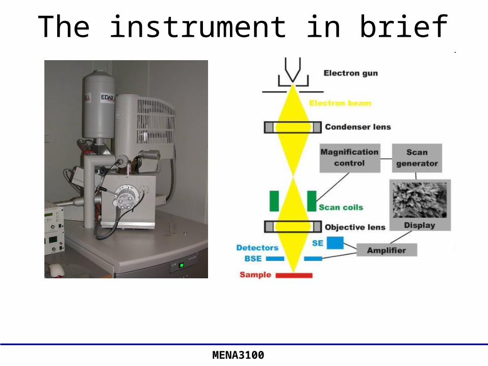
The instrument in brief
MENA3100
How do we get an image?
156 electrons!
Image
Detector
Electron gun288 electrons!
MENA3100
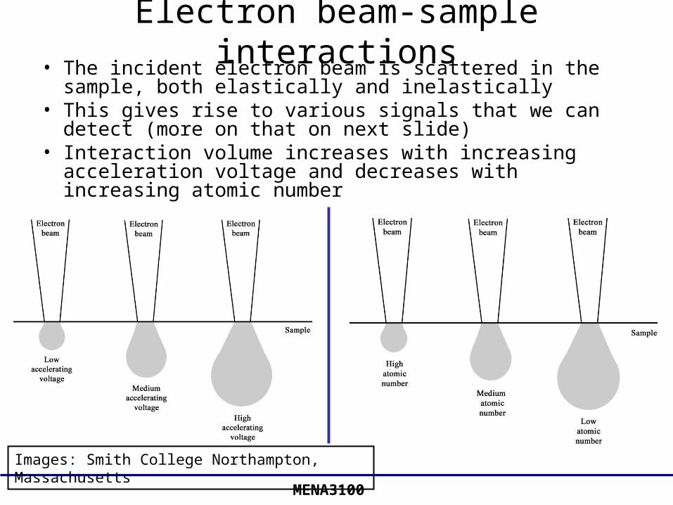
Electron beam-sample interactions• The incident electron beam is scattered in the sample,
both elastically and inelastically• This gives rise to various signals that we can detect
(more on that on next slide)• Interaction volume increases with increasing acceleration
voltage and decreases with increasing atomic number
Images: Smith College Northampton, Massachusetts
MENA3100
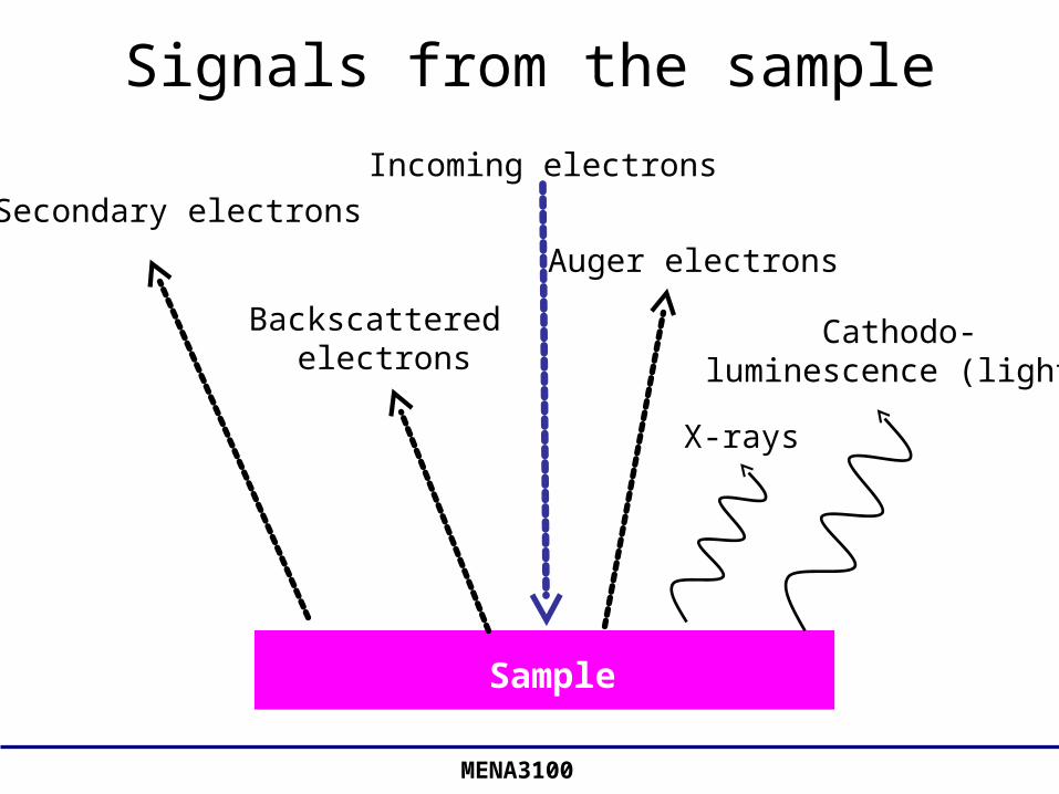
Signals from the sample
Incoming electrons
Secondary electrons
Backscattered electrons
Auger electrons
X-rays
Cathodo-luminescence (light)
Sample
MENA3100
Image: see the text book, page 281.
MENA3100
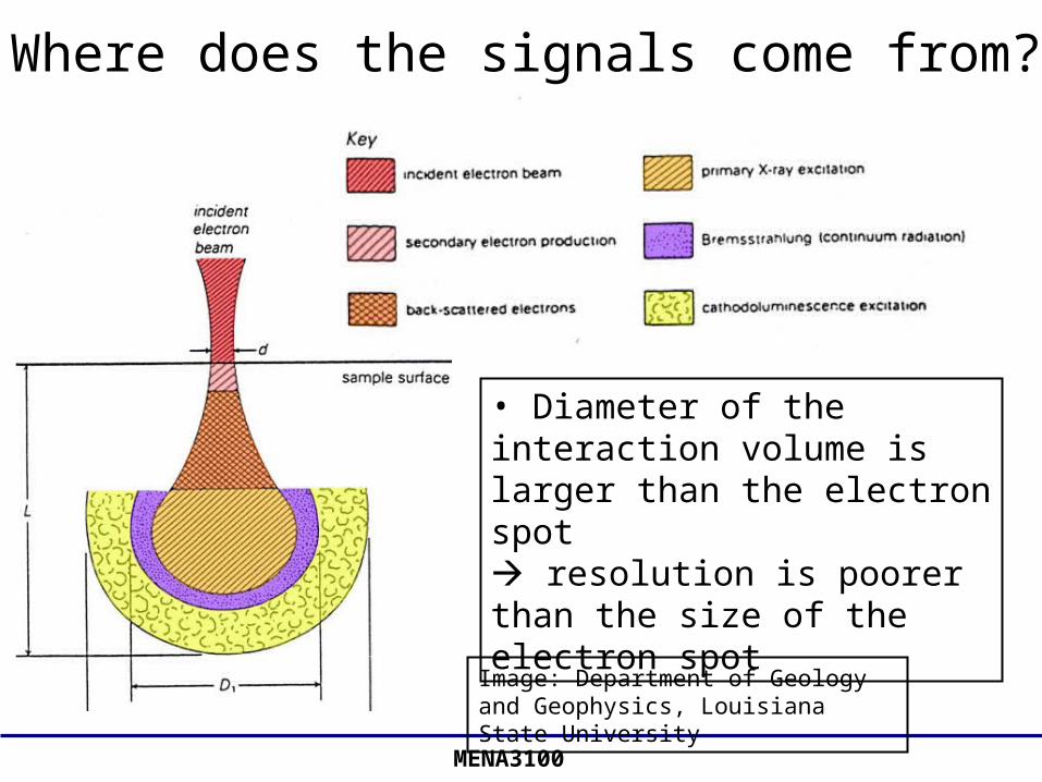
Image: Department of Geology and Geophysics, Louisiana State University
Where does the signals come from?
• Diameter of the interaction volume is larger than the electron spot resolution is poorer than the size of the electron spot
MENA3100
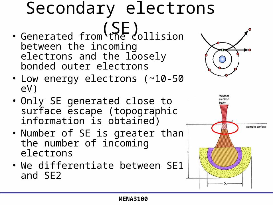
Secondary electrons (SE)• Generated from the collision
between the incoming electrons and the loosely bonded outer electrons
• Low energy electrons (~10-50 eV)• Only SE generated close to
surface escape (topographic information is obtained)
• Number of SE is greater than the number of incoming electrons
• We differentiate between SE1 and SE2
MENA3100
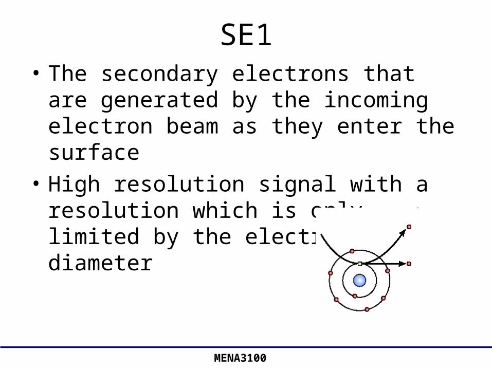
SE1• The secondary electrons that are
generated by the incoming electron beam as they enter the surface
• High resolution signal with a resolution which is only limited by the electron beam diameter
MENA3100
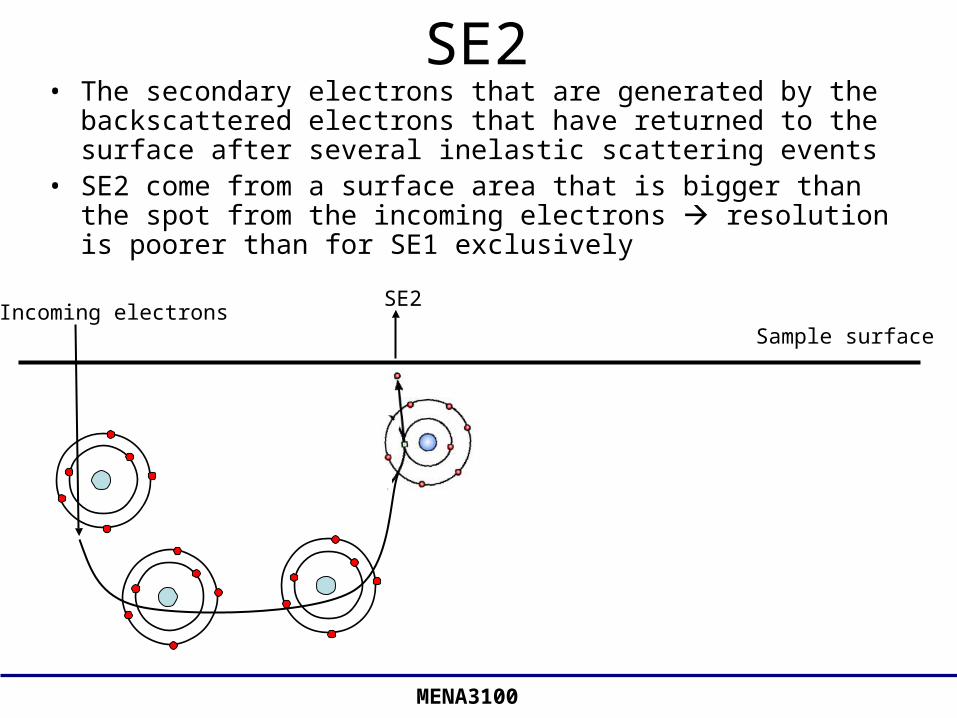
SE2• The secondary electrons that are generated by the
backscattered electrons that have returned to the surface after several inelastic scattering events
• SE2 come from a surface area that is bigger than the spot from the incoming electrons resolution is poorer than for SE1 exclusively
Sample surfaceIncoming electrons
SE2

MENA3100
Factors that affect SE emission1. Work function of the surface2. Beam energy and beam current
• Electron yield goes through a maximum at low acc. voltage, then decreases with increasing acc. voltage (page 283)
Incident electron energy / kV
Sec
onda
ryel
ectr
on y
ield
MENA3100
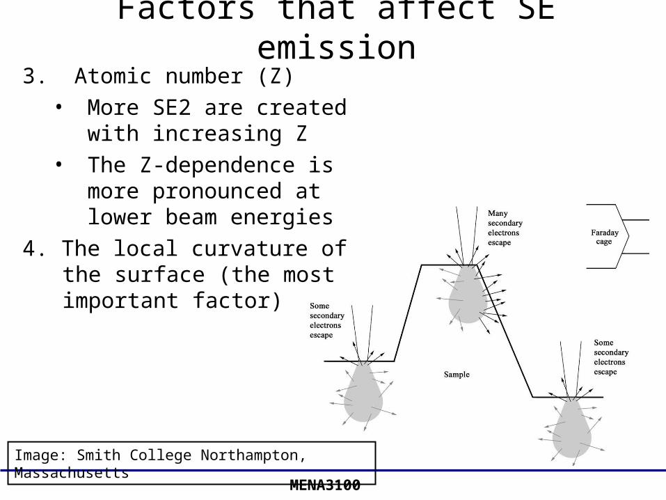
Factors that affect SE emission
3. Atomic number (Z)
• More SE2 are created with increasing Z
• The Z-dependence is more pronounced at lower beam energies
4. The local curvature of the surface (the most important factor)
Image: Smith College Northampton, Massachusetts
MENA3100
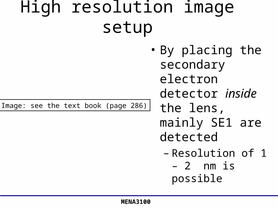
High resolution image setup
• By placing the secondary electron detector inside the lens, mainly SE1 are detected– Resolution of 1 – 2
nm is possible
Image: see the text book (page 286)
MENA3100
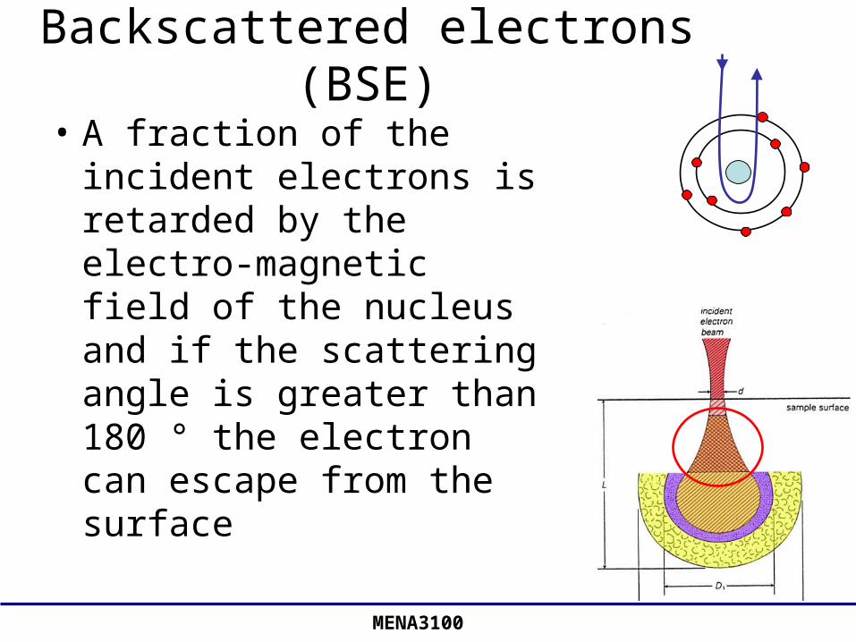
Backscattered electrons (BSE)
• A fraction of the incident electrons is retarded by the electro-magnetic field of the nucleus and if the scattering angle is greater than 180 ° the electron can escape from the surface

MENA3100
Backscattered electrons (BSE)• High energy electrons (elastic scattering)• Fewer BSE than SE• We differentiate between BSE1 and BSE2
Image: See the text book, page 281.
MENA3100
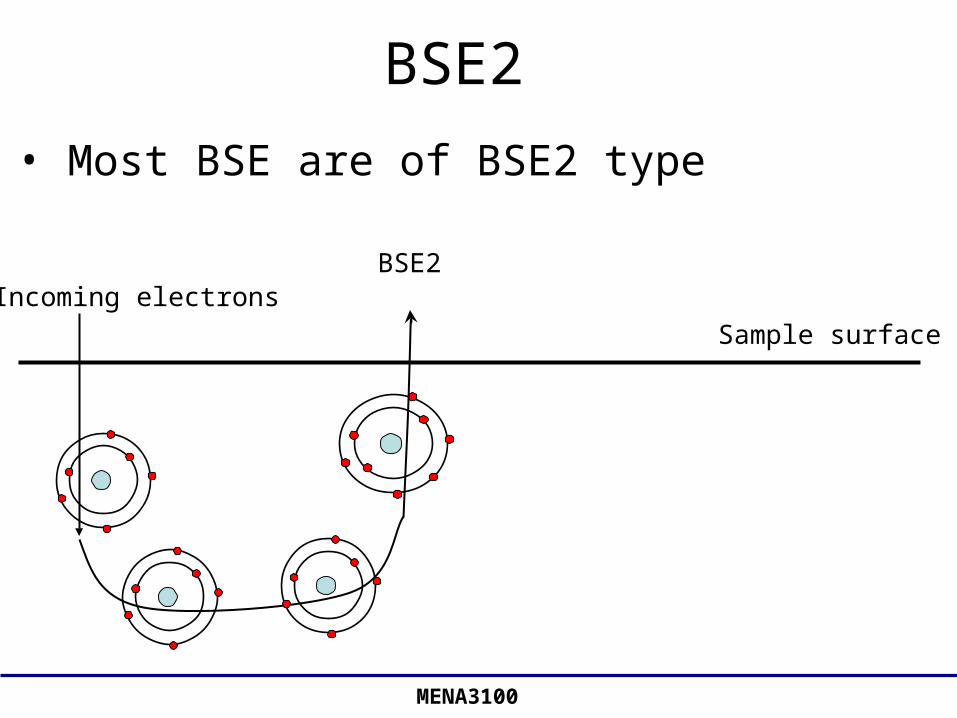
BSE2
Sample surface
Incoming electronsBSE2
• Most BSE are of BSE2 type
MENA3100
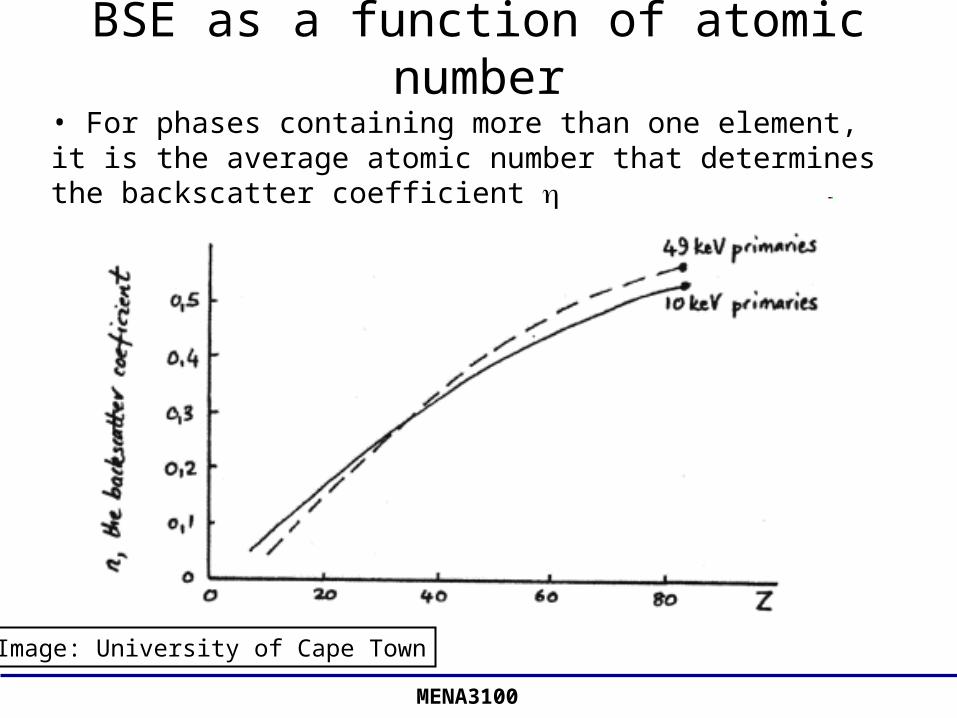
BSE as a function of atomic number
Image: University of Cape Town
• For phases containing more than one element, it is the average atomic number that determines the backscatter coefficient
MENA3100
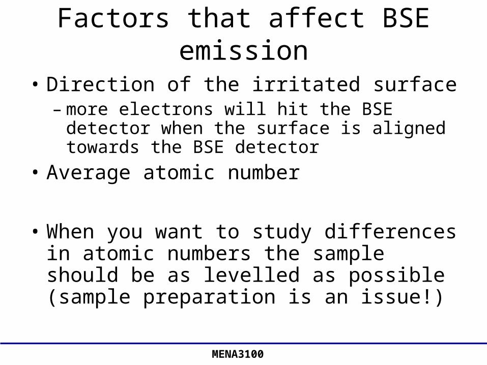
Factors that affect BSE emission
• Direction of the irritated surface– more electrons will hit the BSE detector when
the surface is aligned towards the BSE detector
• Average atomic number
• When you want to study differences in atomic numbers the sample should be as levelled as possible (sample preparation is an issue!)
MENA3100
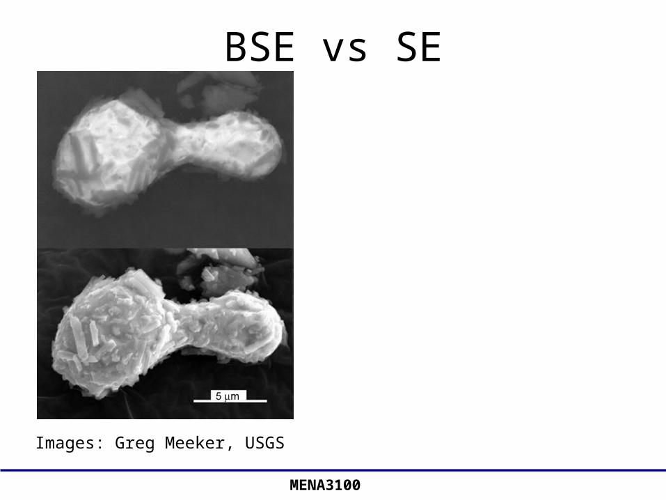
BSE vs SE
Images: Greg Meeker, USGS
MENA3100
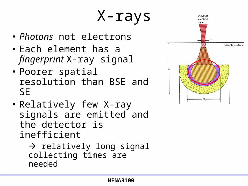
X-rays• Photons not electrons• Each element has a
fingerprint X-ray signal• Poorer spatial resolution
than BSE and SE• Relatively few X-ray signals
are emitted and the detector is inefficient
relatively long signal collecting times are needed

MENA3100
X-rays
• Most common spectrometer: EDS (energy-dispersive spectrometer)
• Signal overlap can be a problem
• We can analyze our sample in different modes– spot analysis– line scan– chemical concentration map (elemental
mapping)
MENA3100
Considerations when using EDS
• Dead time – some twenty-thirty percent is ok
• Statistics– Signal-to-noise ratio
• Drift in electron beam with time
• Build-up of a carbonaceous contamination film after extended periods of electron probe irradiation
MENA3100
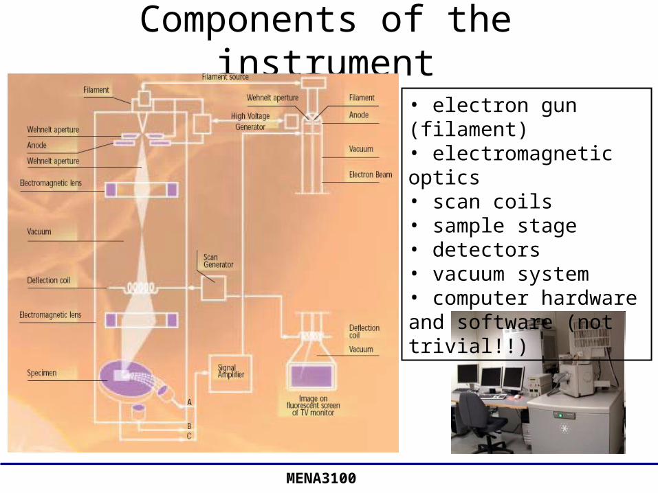
Components of the instrument
• electron gun (filament)• electromagnetic optics• scan coils• sample stage• detectors• vacuum system• computer hardware and software (not trivial!!)

MENA3100
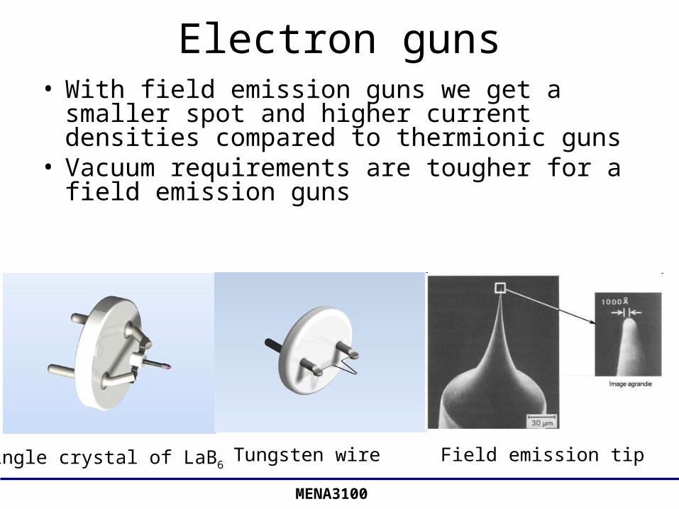
Electron guns• We want many electrons per
time unit per area (high current density) and as small electron spot as possible
• Traditional guns: thermionic electron gun (electrons are emitted when a solid is heated)– W-wire, LaB6-crystal
• Modern: field emission guns (FEG) (cold guns, a strong electric field is used to extract electrons)– Single crystal of W, etched to a
thin tip
MENA3100
Electron guns• With field emission guns we get a smaller spot
and higher current densities compared to thermionic guns
• Vacuum requirements are tougher for a field emission guns
Single crystal of LaB6Tungsten wire Field emission tip
MENA3100
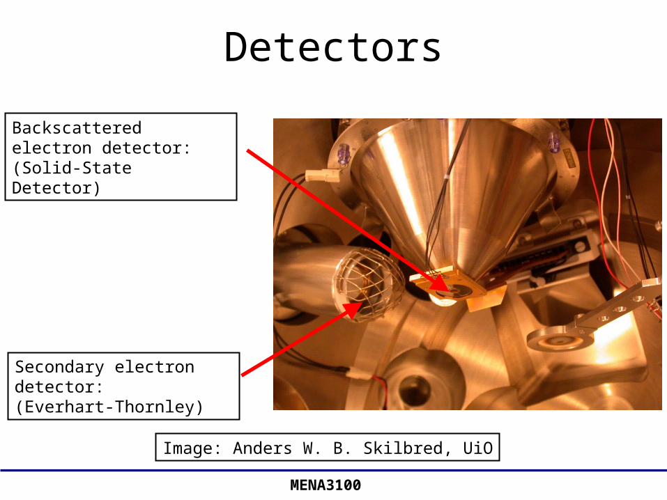
Detectors
Image: Anders W. B. Skilbred, UiO
Secondary electron detector:(Everhart-Thornley)
Backscattered electron detector:(Solid-State Detector)
MENA3100
Our traditional detectors
• Secondary electrons: Everhart-Thornley Detector
• Backscattered electrons: Solid State Detector
• X-rays: Energy dispersive spectrometer (EDS)

MENA3100
Why do we need vacuum?
• Chemical (corrosion!!) and thermal stability is necessary for a well-functioning filament (gun pressure)– A field emission gun requires ~ 10-10 Torr
– LaB6: ~ 10-6 Torr
• The signal electrons must travel from the sample to the detector (chamber pressure)– Vacuum requirements is dependant of the
type of detector
MENA3100
Environmental SEM: ESEM
• Traditional SEM chamber pressure: ~ 10-6
Torr
• ESEM: 0.08 – 30 Torr
• Various gases can be used
• Requires different SE detector

MENA3100
Why ESEM?
• To image challenging samples such as:– insulating samples– vacuum-sensitive samples (e.g. biological samples)– irradiation-sensitive samples (e.g. thin organic films)– “wet” samples (oily, dirty, greasy)
• To study and image chemical and physical processes in-situ such as:– mechanical stress-testing– oxidation of metals– hydration/dehydration (e.g. watching paint dry)
MENA3100
Our instrument: Quanta 200, FEI
• Field emission gun, but no in-lens detector
• ESEM
• Can be equipped with various accessories to perform in-situ experiments (more on this on next slide)
MENA3100
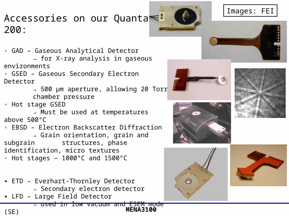
Accessories on our Quanta 200:
◦ GAD – Gaseous Analytical Detector → for X-ray analysis in gaseous environments
◦ GSED – Gaseous Secondary Electron Detector→ 500 μm aperture, allowing 20 Torr
chamber pressure◦ Hot stage GSED
→ Must be used at temperatures above 500°C◦ EBSD – Electron Backscatter Diffraction
→ Grain orientation, grain and subgrain structures, phase identification, micro textures ◦ Hot stages – 1000°C and 1500°C
▪ ETD – Everhart-Thornley Detector→ Secondary electron detector
▪ LFD – Large Field Detector → used in low vacuum and ESEM mode (SE)
▪ SSD-BSD – Solid State Backscattered Detector→ Backscatter electrons
▪ EDS – Energy dispersive spectroscopy→ X-ray analysis
Images: FEI
MENA3100
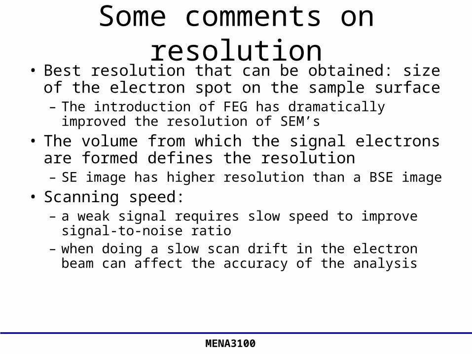
Some comments on resolution• Best resolution that can be obtained: size of the
electron spot on the sample surface– The introduction of FEG has dramatically improved
the resolution of SEM’s
• The volume from which the signal electrons are formed defines the resolution– SE image has higher resolution than a BSE image
• Scanning speed: – a weak signal requires slow speed to improve signal-
to-noise ratio– when doing a slow scan drift in the electron beam can
affect the accuracy of the analysis
MENA3100
What have we not covered in this presentation
• Sample preparation
• Details on the electromagnetic optics
• Alternative imaging modes:– Cathodoluminescence– Electron beam induces current– Orientation imaging microscopy (available at
UiO)
• Focused ion beam microscopy
MENA3100
Summary
• The scanning electron microscope is a versatile instrument that can be used for many purposes and can be equipped with various accessories
• An electron probe is scanned across the surface of the sample and detectors interpret the signal as a function of time
• A resolution of 1 – 2 nm can be obtained when operated in a high resolution setup
• The introduction of ESEM and the field emission gun have simplified the imaging of challenging samples

MENA3100
Summary• Signals:
– Secondary electrons (SE): mainly topography
• Low energy electrons, high resolution• Surface signal dependent on curvature
– Backscattered electrons (BSE): mainly chemistry
• High energy electrons• “Bulk” signal dependent on atomic number
– X-rays: chemistry• Longer recording times are needed