MEMS II: March 5, 2012 - colorado.edu II: March 5, 2012 ... 8 – 30 GHz S 21 (dB) ... Active...
53
MEMS II: March 5, 2012 • Literature Review #6 • Literature Review #5 Aptamers on a Microchip • MEMS Packaging 1
Transcript of MEMS II: March 5, 2012 - colorado.edu II: March 5, 2012 ... 8 – 30 GHz S 21 (dB) ... Active...

MEMS II: March 5, 2012
• Literature Review #6• Literature Review #5
Aptamers on a Microchip• MEMS Packaging
1

REMOTE CONTROL OF A CYBORG MOTH USING CARBON NANOTUBE-ENHANCED FLEXIBLE NEUROPROSTHETIC PROBE
• W.M. Tsang1, A. Stone2, Z. Aldworth3, D. Otten1, A.I. Akinwande1, T. Daniel3, J.G.
• Hildebrand2, R.B. Levine2, J. Voldman1• 1Massachusetts Institute of Technology,
Cambridge, MA, USA• 2University of Arizona, Tucson, AZ, USA• 3University of Washington, Seattle, WA,
USA2Literature review #6

ISOLATION OF THERMALLY SENSITIVE APTAMERS ON A MICROCHIP
• J. P. Hilton1, Jinho Kim1, ThaiHuuNguyen1, Mihaela Barbu2,
• Renjun Pei2, Milan Stojanovic2, and QiaoLin1
• 1Department of Mechanical Engineering,• 2Department of Medicine, Columbia
University, New York, USA
3

4

5

6

7

8

9

10

11

12

13

Packaging and Microelectromechanical Systems (MEMS)
Y. C. LeeDepartment of Mechanical Engineering
University of Colorado, Boulder, Colorado 80309-0427, USA

Packaging of MEMS• Wafer level packaging• Integration using flip-chip assembly Packaging for MEMS• Flexible circuits for MEMSMEMS for Packaging • Active alignment for optoelectronic packagingFuture• Integrated MEMS Device and Package• Integrated MEMS/NEMS
Contents

Microelectromechanical Systems (MEMS)
Solid modelingElectro-thermal-mechanical coupling
Thick layersMechanical properties
Sacrificial materials removed during release
Testing Dicing
Assembly, sealing, testing and reliability
Solid modelingElectro-thermal-mechanical coupling
Thick layersMechanical properties
Sacrificial materials removed during release
Testing Dicing
Assembly, sealing, testing and reliability
Solid modelingElectro-thermal-mechanical coupling
Thick layersMechanical properties
Sacrificial materials removed during release
Testing Dicing
Assembly, sealing, testing and reliability
?

BondingCap
State-of-the-Art Wafer-Level Capping

State-of-the-ArtIntel Microshell Package for RF MEMS
John Heck, et al., ASME InterPACK’07

MEMS Device/Package Fabricated on Wafer
Device + Package
MEMS + CMOS
Kurt Petersen, SiTime, Jan. 2007.Tom Kenny’s group, InterPACK’01- InterPACK’07
Wafer Level MEMS Packaging
Literature review assigned.

Polymer MEMS Package

Atomic Layer Deposition (ALD) for Hermetic Sealing of Wafer Level Polymer Package
0.0001
0.001
0.01
0.1
1
10
0 5 10 15 20 25 30Alumina ALD Thickness (nm)
Per
mea
tion
Rat
eW
VTR
(g/m
2/da
y) H
TO te
st Polymer Film
ALD-on-Polymer Film
Polymer
Solder Bumps
ALD-alumina
0.00001 possible

Thermal and Vibration Isolation

BioMEMS

Packaging of MEMS• Wafer level packaging• Integration using flip-chip assemblyPackaging for MEMS• Flexible circuits for MEMSMEMS for Packaging • Active alignment for optoelectronic packagingFuture• Integrated MEMS Device and Package• Integrated MEMS/NEMS
Contents

MEMS Integrated with Other Components
MEMS Variable Capacitors

Tethers and Posts for Flip-Chip Assembly
Gap?

MEMS Designed for Flip-Chip Assembly

Post-Enabled Gap Control

Tethers
Mechanical Stops
Locking Bumps
Tethers
Mechanical Stops
(a) Layout of a successful tether design.
(b) Cross-sectional view of the tether design in (a-a).
(c) SEM photograph of successful tethers.
a a

Flip-Chip Assembly

Flip-Chip Bonding:
• Flip-chip bond micromirror chip to substrate
• Etch sacrificial oxide to free the silicon chip
Ceramic Substrate Flip-Chip Bonding Results

Packaging of MEMS• Wafer level packaging• Integration using flip-chip assembly Packaging for MEMS• Flexible circuits for MEMSMEMS for Packaging • Active alignment for optoelectronic packagingFuture• Integrated MEMS Device and Package• Integrated MEMS/NEMS
Contents

On-chip Variable Capacitor Berkeley Group Raytheon Switch
On-Chip MUMPSVariable CapacitorColumbia Univ.
Area Tuned Variable Capacitors
Plate Motion
CU Variable Capacitor (thermal actuation)
CU Variable CapacitorElectrostatic (1-D)
Si- or GaAs-Based RF MEMS
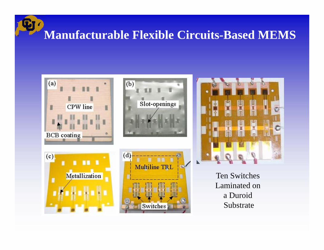
Manufacturable Flexible Circuits-Based MEMS
Ten Switches Laminated on
a Duroid Substrate

S 21
(dB
)
Capacitive Switch: 8 – 30 GHz
S 21
(dB
)
CPW Design:
W=1.6 mm, and G=100 μm
Switch electrode Design:
l = 2.0 mm, and w = 1.0 mmDown Position: Isolation
l
w
W GG
Frequency (GHz)
MeasuredEM simulation
Measured
EM simulationFitted Model*
Up position: Insertion loss
Performance SummaryInsertion loss < 0.3-0.4 dB
Isolation > 15 dB @ 12 GHz, 36 dB @ 30 GHz

Packaging of MEMS• Wafer level packaging• Integration using flip-chip assembly Packaging for MEMS• Flexible circuits for MEMSMEMS for Packaging • Active alignment for optoelectronic packagingFuture• Integrated MEMS Device and Package• Integrated MEMS/NEMS
Contents

Active Alignment and Laser Welding
Laser Welding MachineActive alignment
FiberSearching pattern
Laser Beam
Newport Corporation, 2001. http://www.newport.com
Hammering

Paradigm Shift in Automation?
Large expensive machinesfor sub-um precision alignments? Hundreds of micro-machines
for sub-um precision alignments!

MEMS-Enabled Laser-to-Fiber Coupling

Tethered Bimorph for Active Alignment and Position Fixing
Tethers
Bimorph
Tip Deflection 6030150 45 µm

Mirror with Tethered Bimorph

Mirror with Tethered Bimorph
Roll

Mirror with Tethered Bimorph
Pitch

ExperimentReflected Beam Angles
-5.0
0.0
5.0
10.0
15.0
20.0
25.0
30.0
-5.0 0.0 5.0 10.0
Roll (deg)
Pit
ch (
deg) Device 1
Device 2Device 3
Target

Experiment

Experimental Results – Step 1Target
Reflected Beam Angles
-5.0
0.0
5.0
10.0
15.0
20.0
25.0
30.0
-5.0 0.0 5.0 10.0
Roll (deg)
Pit
ch (
deg) Device 1
Device 2Device 3

Experimental Results – Step 2Target
Reflected Beam Angles
-5.0
0.0
5.0
10.0
15.0
20.0
25.0
30.0
-5.0 0.0 5.0 10.0
Roll (deg)
Pit
ch (
deg) Device 1
Device 2Device 3

Experimental Results – Step 3Target
Reflected Beam Angles
-5.0
0.0
5.0
10.0
15.0
20.0
25.0
30.0
-5.0 0.0 5.0 10.0
Roll (deg)
Pit
ch (
deg) Device 1
Device 2Device 3

Movements with Large-Degree of Freedom
for Optimum Alignment
0
2
4
6
8
10
12
-5 -4 -3 -2 -1 0 1 2 3Ro l l ( d eg )
Pi
tc
h
(d
eg
)

Packaging of MEMS• Wafer level packaging• Integration using flip-chip assembly Packaging for MEMS• Flexible circuits for MEMSMEMS for Packaging • Active alignment for optoelectronic packagingFuture• Integrated MEMS Device and Package• Integrated MEMS/NEMS
Contents

Cooler Assembly
51

Stable Cryogenic Cooling Demonstrated
Compressor Overheat
Pressure ratio =16.7 : 0.87 (atm)
Pressure ratio slowly increased
Feasible but unstable operation with low pressure level changed20 min
52

Packaging of MEMS• Wafer level packaging• Integration using flip-chip assembly Packaging for MEMS• Flexible circuits for MEMSMEMS for Packaging • Active alignment for optoelectronic packagingFuture• Integrated MEMS Device and Package• Integrated MEMS/NEMS
SummaryGreat Challenges/Opportunities
for Packaging Engineers